PANJIT 1SMC5388, 1SMC5387, 1SMC5376, 1SMC5375, 1SMC5374 Datasheet
...
1SMC5348 THRU 1SMC5388
FEATURE
S
MECHANICAL DATA
MAXIMUM RATINGS AND ELECTRICAL CHARACTERISTIC
S
D
FSM
STG
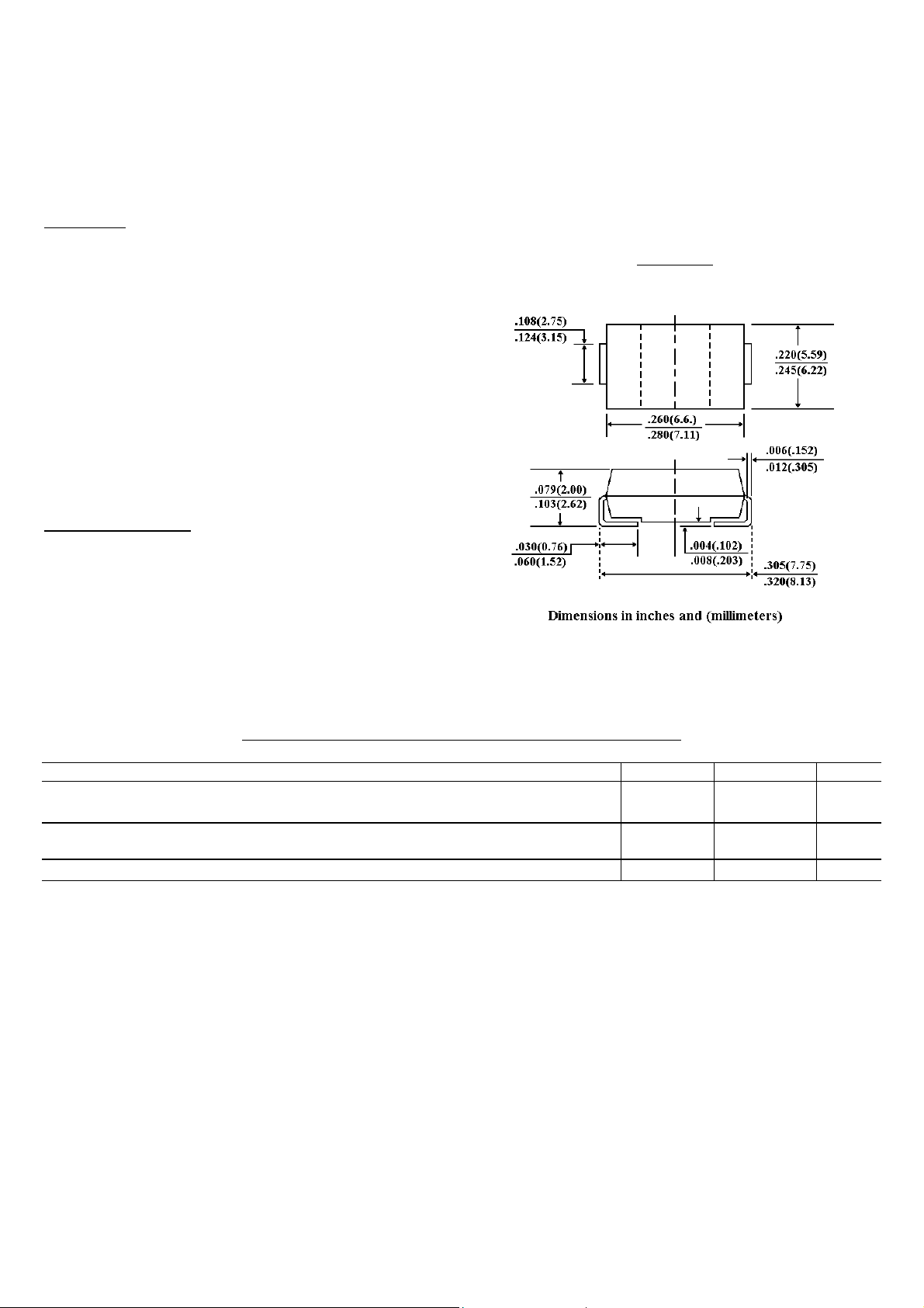
DO-214A
B
SURFACE MOUNT SILICON ZENER DIODE
VOLTAGE - 11 TO 200 Volts Power - 5.0 Watts
l
For surface mounted applications in order to
optimize board space
l
Low profile package
l
Built-in strain relief
l
Glass passivated junction
l
Low inductance
l Typical ID less than 1 £gA above 13V
l
High temperature soldering :
260 ¢J/10 seconds at terminals
l
Plastic package has Underwriters Laboratory
Flammability Classification 94V-O
Case: JEDEC DO-214AB Molded plastic
over passivated junction
Terminals: Solder plated, solderable per
MIL-STD-750, method 2026
Standard Packaging: 16mm tape(EIA-481)
Weight: 0.007 ounce, 0.21 gram
Ratings at 25¢Jambient temperature unless otherwise specified.
SYMBOL VALUE UNITS
DC Power Dissipation @ TL=75 ¢J, Measure at Zero Lead Length(Fig. 1)
Derate above 75¢J(Note 1)
Peak forward Surge Current 8.3ms single half sine-wave superimposed on rated
load(JEDEC Method) (Note 1,2)
Operating Junction and Storage Temperature Range TJ,T
NOTES:
1. Mounted on 8.0mm2 copper pads to each terminal.
2. 8.3ms single half sine-wave, or equivalent square wave, duty cycle = 4 pulses per minute maximum.
P
I
See Fig. 5 Amps
-55 to +150 ¢J
5.0
40.0
Watts
mW/¢J

1SMC5348 THRU 1SMC538
8
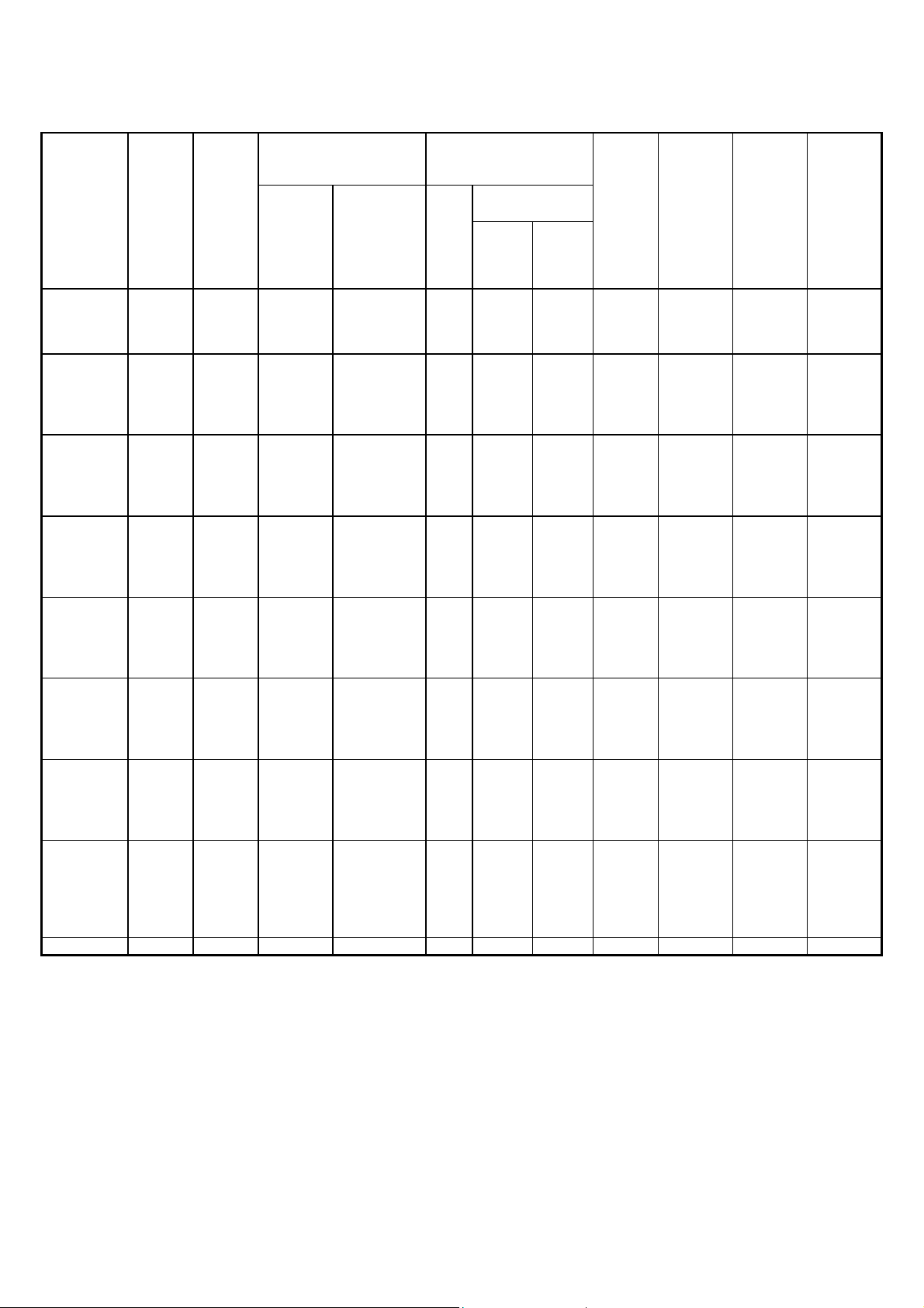
ELECTRICAL CHARACTERISTICS (TA=25¢Junless otherwise noted, VF=1.2 Max @
IF=1A for all types
.
Maximum ZenerImpedanceMax reverseLeakage Curren
t
@ V
R
Volts
Type No.(Note 1.)NominalZener
Voltage
Vz @
I
Z
T
volts(Note 2.)Testcurrent
I
Z
T
m
A
Z
Z
T
@
I
Z
T
Ohms(Note 2.)
Z
Z
k
@
I
Z
K
= 1mAOhms(Note 2.)
I
R
£g
ANon & ASuffixB-Suffi
x
MaxSurg
e
Current
Ir Amps(Note 3.)MaxVoltag
e
Regulatio
n
Vz, Volts(Note 4.)MaximumRegulato
r
Current
I
Z
M
mA(Note 5.)DeviceMarking
Code1SMC534
8
1SMC53491SMC53501SMC535
1
1
1
12131
4
125
100100100
2.5
2.52.52.5
125
1251007
5521188.69.410.
1
8.4
9.19.910.
687.576.7
0.2
5
0.250.250.2
5
430
395365340
348
B
349B350B351B1SMC53521SMC53531SMC535
4
1SMC535
5
1SMC535615161
7
1
8
1975757
0
6
5
652.52.52.5
2.5
3757575
7
5
75110.5
0.5
0.510.811.512.2
1
3
13.711.512.212.
9
13.
7
14.46.365.8
5.5
5.30.250.30.3
5
0.4
0.431529528
0
265
250352B353B354B
355
B
356B1SMC53571SMC535
8
1SMC535
9
1SMC53601SMC5361202
2
2
4
2527655
0
5
0
505033.
5
3.5
45757
5
100
1101200.50.
5
0.5
0.50.514.415.
8
17.
3
1819.415.216.
7
18.
2
1920.65.14.
7
4.4
4.34.10.40.45
0.5
5
0.550.6237216
198
190176357B358
B
359
B
360B361
B
1SMC536
2
1SMC53631SMC53641SMC536
5
1SMC53662
8
30333
6
395
0
40403
0
306
81011
14130
140150160
1700.
5
0.50.50.5
0.520.1
21.623.825.
9
28.121.
2
22.825.127.
4
29.73.9
3.73.53.3
3.10.
6
0.60.60.6
5
0.65170
158144132
122362B
363B364B365
B
366
B
1SMC53671SMC536
8
1SMC536
9
1SMC53701SMC5371434
7
5
1
5660302
5
2
5
2020202
5
2
7
354019021
0
230
2803500.50.
5
0.5
0.50.53133.
8
36.
7
40.34332.735.
8
38.
8
42.645.52.82.
7
2.5
2.32.20.70.
8
0.9
11.211010
0
9
3
8679367B368
B
369
B
370B371
B
1SMC537
2
1SMC53731SMC53741SMC537
5
1SMC53766
2
68758
2
872
0
20201
5
154
2
44456
5
75400
500620720
7600.
5
0.50.50.5
0.544.6
49545
9
6347.
1
51.75662.
2
662.1
21.91.8
1.71.35
1.51.61.8
276
70635
8
54.5372
B
373B374B375
B
376
B
1SMC53771SMC537
8
1SMC537
9
1SMC53801SMC538191100
110
120130151
2
1
2
1010759
0
125
17019076080
0
100
0
115012500.50.
5
0.5
0.50.565.57
2
79.
2
86.493.669.27
6
83.
6
91.298.81.61.
5
1.4
1.31.22.22.
5
2.5
2.52.552.547.
5
4
3
39.536.6377B378
B
379
B
380B381
B
1SMC538
2
1SMC53831SMC53841SMC53851SMC538
6
1SMC5387140
15016017018
0
190
8
888
5
523
0
33035038043
0
4501500
150016501750175
0
18500.5
0.50.50.50.
5
0.510
1
10811512213
0
13710
6
11412212913
7
1441.
2
1.11.11
1
0.92.
5
333
4
534
31.629.42826.
4
25382
B
383B384B385B386
B
387
B
1SMC5388200548018500.51441520.9523.6388
B
£G
NOTE:
1. TOLERANCE AND VOLTAGE DESIGNATION - The JEDEC type numbers shown indicate a tolerance of ¡Ó 10% with
guaranteed limits on only Vz, IR, Ir, and VF as shown in the electrical characteristics table. Units with guaranteed
limits on all seven parameters are indicated by suffix “B” for ¡Ó 5% tolerance.
2. ZENER VOLTAGE (Vz) AND IMPEDANCE (ZZT & ZZK) - Test conditions for Zener voltage and impedance are as
follows; Iz is applied 40 ¡Ó 10 ms prior to reading. Mounting contacts are located from the inside edge of mounting
clips to the body of the diode.(TA=25 ¢J
¡Ï¢·
¡Ð¢±
¢J).
 Loading...