

Page 1
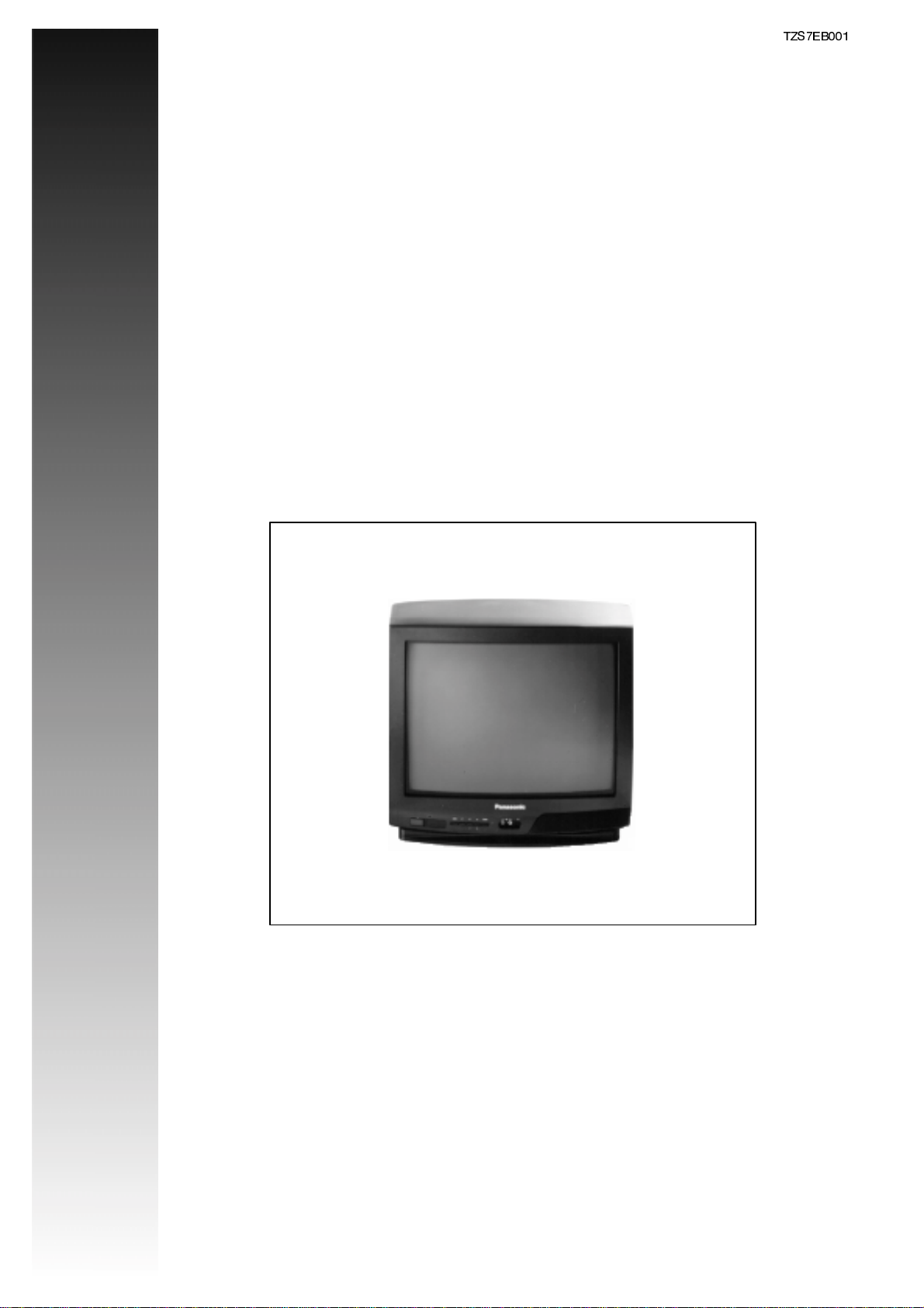
7HFKQLFDO *XLGH
Contents
&RORXU 7HOHYLVLRQ
= &KDVVLV
&LUFXLW ([SODQDWLRQV
7=6(%
3DQDVRQLF
(XURSHDQ 7HOHYLVLRQ 'LYLVLRQ
0DWVXVKLWD (OHFWULF 8. /WG
Page 2

3DQDVRQLF
CONTENTS
1. Introduction 3........................................................
2. Features 4...........................................................
2.1. Differences 4..........................................................
3. Block Diagrams 5....................................................
3.1. Control Block Diagram 5................................................
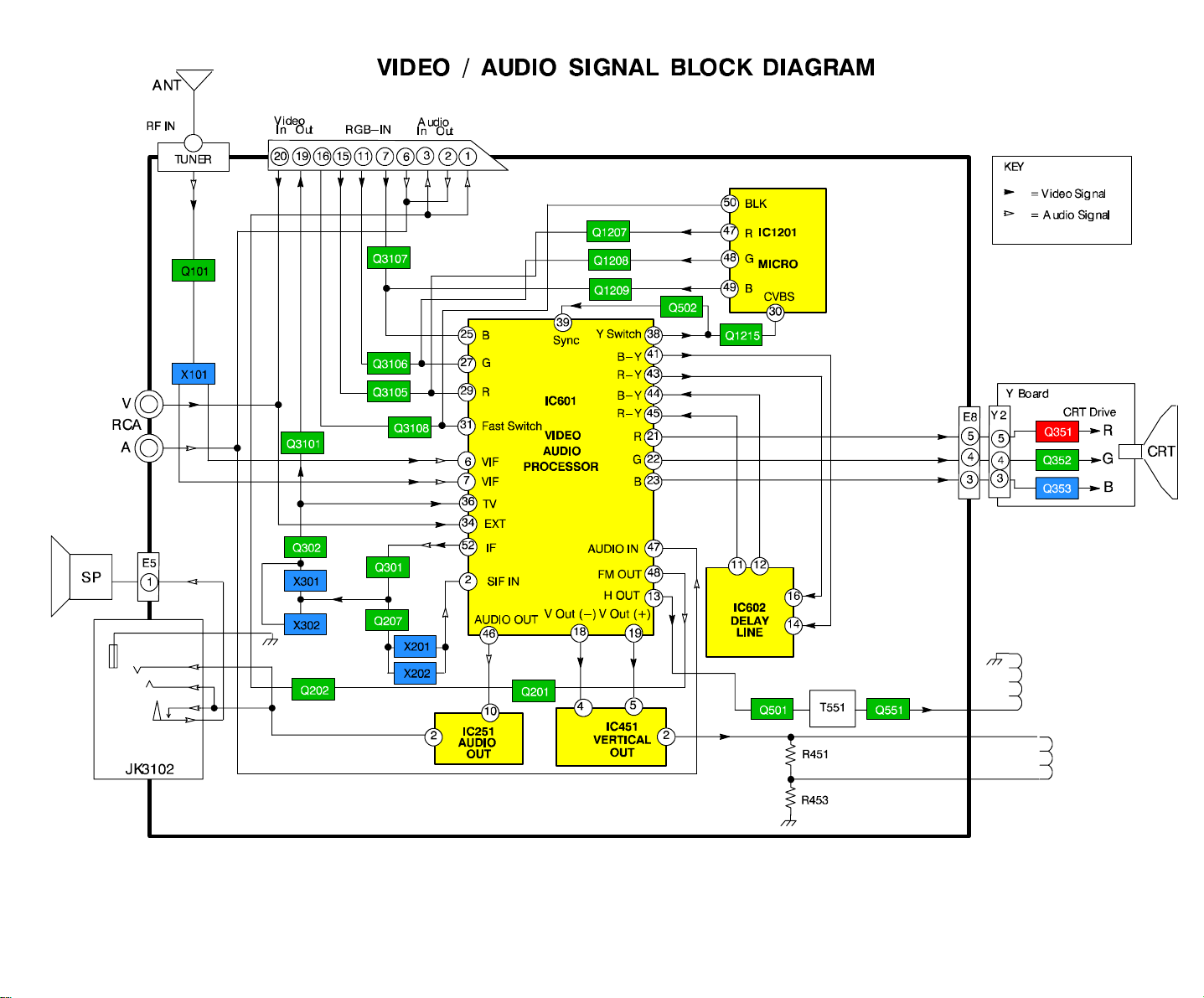
3.2. Video and Audio Block Diagram 6........................................
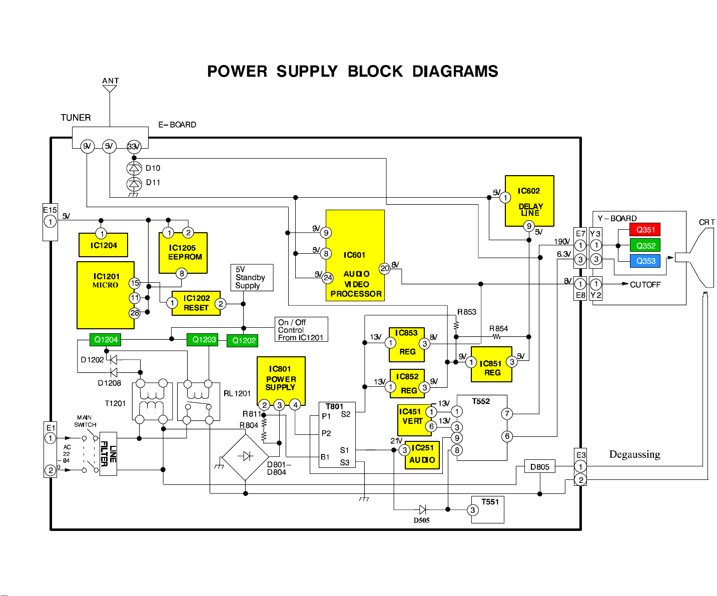
3.3. Power Supply Block Diagram 7..........................................
4. Power Supply 8......................................................
4.1. Standby Power Supply 8................................................
4.2. Power Supply Circuit Operation 9........................................
4.3. Regulation 10..........................................................
4.4. Protection 11...........................................................
4.4.1.Overcurrent 11...................................................................
4.4.2.Overvoltage 11...................................................................
4.5. Secondary Supply Side 11...............................................
5. Microprocessor and Teletext Processing 12............................
5.1. Microprocessor Stage 13................................................
5.1.1.Input Information 13...............................................................
5.1.2.Output Information 14.............................................................
5.1.3.Data Bus Lines 15................................................................
5.2. Teletext Processing 16..................................................
5.2.1.Teletext Operation 16.............................................................
6. Memory (EEPROM) 17.................................................
7. Colour TV Signal Processing 18.......................................
7.1. V.I.F. Processing 19.....................................................
7.2. Video Signal Processing 21..............................................
7.3. Luminance Processing 21................................................
7.4. PAL Chrominance Processing 22.........................................
7.5. SECAM Processing 23..................................................
7.6. RGB Input 23..........................................................
7.7. Audio Processing 24....................................................
7.8. Deflection Processing 25................................................
7.8.1.Horizontal Processing 25..........................................................
7.8.2.Vertical Processing 25.............................................................
8. Baseband Delay Line 26...............................................
8.1. Operation 26...........................................................
9. SECAM Chrominance Processor 27....................................
10. Horizontal Output 28..................................................
11. Vertical Output 29.....................................................
11.1. Vertical Protection 30....................................................
12. Beam Current Limiting 31..............................................
13. A.F. Output Stage 32..................................................
14. Appendices 33........................................................
Page 3

1. Introduction
3DQDVRQLF
We at Panasonic realise that the service engineer
needs to understand the circuitry inside the TV and
forthisneed,wehaveproducedthisTechnical Guide.
This Technical Guide contains information for Z7
chassis and should be used inconjunction with the
relevant Service Manuals for this chassis.
Page 4

3DQDVRQLF
2. Features
The following features listed below are new to this model range which comprise of the following:
: New switch mode power supply witha1wattstandby circuit
: New microprocessor, with built in teletext processing
: New one chip IC processing
: All alignments which are software controlled, except the Horizontal width for 21” (55cm) models
: Automatic Tuning Procedure (ATP) function
: New On Screen Display (OSD)
2.1. Differences
The major differences to Z5 are as follows:
: Low power consumption in standby (1watt)
: Power supply is switched off during standby mode
: Split DC supply used for the vertical output stage
: Improved circuit protection
: Software controlled alignments
Page 5
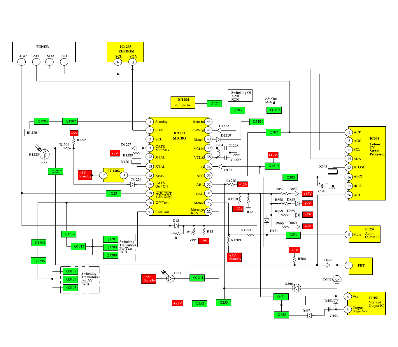
CONTROL LINE BLOCK DIAGRAM
Page 6
Page 7
Page 8
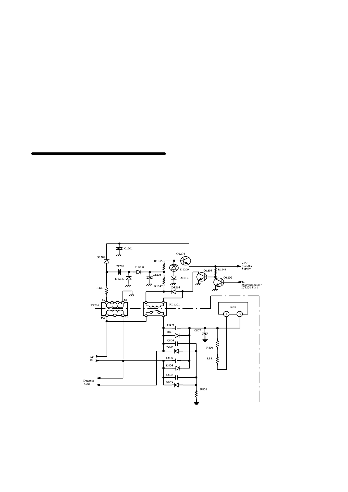
3DQDVRQLF
4. POWER SUPPLY
The mains A.C. voltage used for Z7 is fed via
connector E1 situated on the E-Board. From the
connector E1 the mains A.C. power supply is fed via
the main TV On/Off switch S801 and two line
suppression filters L801/L802beforebeingfedtothe
standby transformer T1201.
At the standby transformer T1201 the A.C. supply
splits into two paths.
The first path sees the A.C. supply being fed to the
normally open contact of the standby relay RL1201,
while the second path has the A.C. supply being fed
via the windings P2 / P1 of the standby transformer
T1201 supply.
4.1. Standby Power Supply Circuit
The standby transformer T1201 has the A.C. supply
as just mentioned being fed via the primary winding
P2/P1.
From the output of the secondary windings S2/S1 of
the standby transformer, a 5V standby supply is fed
viaresistor R1201, where the supply takes two paths.
The first path that the standby supply followsis
via capacitor C1202 and rectifying diode D1208, this
supply is then smoothed by capacitor C1203. This
rectified and smoothed supply is then again split into
two paths.
: Thefirstpathseesthesupplyvoltagebeingfed
via resistor R1247 to the standby relay RL1201 and
the relay winding to the collector of transistor Q1203.
Transistor Q1203 which is controlled by Q1202.
Q1202isresponsibleforswitchingtheTVinto andout
of standby under the control of the microprocessor
IC1201 pin 1.
: The second path is via resistor R1246 to the
baseoftransistorQ1204.Thissupplybeingregulated
by the zener diode D1209 is used as a base bias.
The second path from the standby transformer
T1201, that the supply voltage follows is via the
rectifying diode D1202 and smoothing capacitor
C1201. Here the supply is applied to the collector of
Q1204. From the emitter of Q1204 a 5V standby
supply is fed to the Microprocessor IC1201 and the
EAROM IC1205. This supply allows these circuits to
operate during standby which is required to process
the switch ON command from the remote control or
local keys, allowing the TV to be switched out of
standby.
Page 9
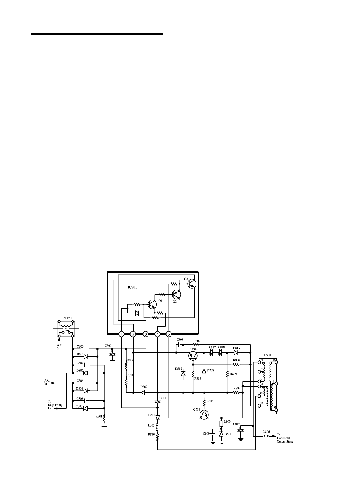
3DQDVRQLF
4.2. Power Supply Circuit Operation
The supply voltage for the main power supply circuit
is fed via the standby relay RL1201 to the bridge
rectifying diodes D801, D802, D803 and D804 where
the A.C. voltage is full rectified and smoothed by
capacitor C807.
This smoothed d.c. voltage of approximately 300V
then follows two paths.
The first path feeds this d.c. supply to pin 3 of the
switched mode power supply IC IC801. Here the d.c.
voltage input via pin 3 is fed to thecollector of internal
transistor Q3.
The second path that the d.c. supply follows is via
resistors R804 and R811 and to pin 2 of IC801.This
supply is used to provide IC801 with a start-upsupply
which is fed to base of internal transistor Q3,
providing base bias.
With Q3 conducting the supply voltage flows via pins
3and4ofIC801 via the primary winding P2/P1 of
transformer T801, building up magnetic energy until
magnetic saturation is reached. This results in no
further supply voltage being fed via the windings
P2/P1 where upon the magnetic field breaks down.
This break down of the magnetic field results in a
transfer of energy from the primary winding to the
secondary winding providing the required secondary
supplies.
The supply voltage flowing via the primary winding
P2/P1 is smoothed by C812 and fed to the horizontal
output stage.
After the start up of the power supply unit the supply
voltage for IC801. is received from the auxiliary
windingB1oftransformerT801which is fedviaR807,
C808 to pin 2 of IC801 and internal transistor Q3.
The supply from B1 of the transformer T801 is
proportional to the supply fed via the primary winding
P2/P1. However winding B1 is unable to supply the
necessary current to switch ON Q3 quickly and for
this purpose transistor Q802 and capacitors C817,
C810 are used.
At start-up Q3 begins to conduct as described above,
withtheconductionofQ3theoutputfrom the auxiliary
winding B1 feeds back a positive supply to pin 2, as
well as feeding this supply back to pin 2 the supply
is also fed to the base of transistor Q802 via resistors
R813, R808. This supply biases Q802 into
conduction which results in capacitors C810 / C817
discharging via the collector - emitter junction to pin
2 and the base of Q3. The rate at which these
capacitors discharge being set by R809.
When the transformer T801 finally reaches magnetic
saturation mentioned previously the output from the
winding B1 begins to reduce, with the reduction in
supplyfrom B1windingthebasebiastoQ3andQ802
are also reduced switching OFF both transistors.
With both transistors switched OFF capacitors C817
/ C810 charge via D808.
When finally Q3 is switched on the cycle just
described is repeated.
Page 10
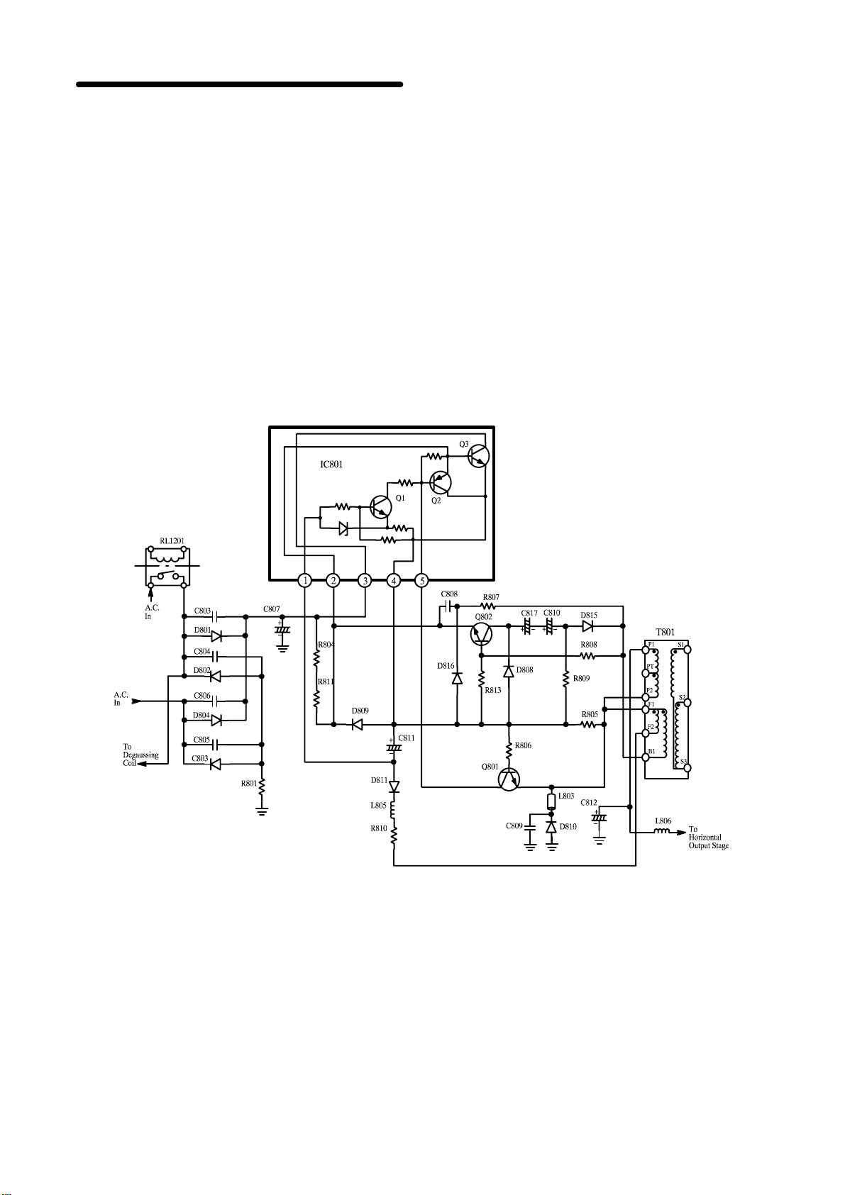
3DQDVRQLF
4.3. Regulation
When the power supply has started and operating
normallyanychanges inload or mains supply voltage
are regulated by auxiliary windings F1/F2 of T801.
This is achieved by controlling the switching
frequency of the power supply.
To do this a negative feedback voltage is fed via
R810, L805 and diode D811to pin 1 of IC801 Q1, this
negative feedback voltage is then used to control the
bias of internal transistor Q1.
The internal transistor Q1 is biased On by the output
supply fed from the emitter of internal transistor Q3.
This means that as the output from Q3 increases or
decrease so does the bias of Q1.
If the output from Q3 increases Q1 conducts more,
thisresultsinthebaseofQ2becomingmorenegative
with respect to its emitter causing Q2 to conduct.
When Q2 conducts the base bias of Q3 is reduced
keeping the output from pin 4 constant.
If however the load on the transformer T801
increases this demand has to be met and the effect
ofQ1onQ3 reduced.Thisisachievedbythe negative
feedback fed from the auxiliary winding F1/F2 to pin
1ofIC801.
When an increase in current load occurs on T801 the
negative feedback voltage applied to pin 1 of IC801
will become more negative. The more negative the
feedback voltage becomes, the less Q1 and Q2
conduct enabling Q3 to conduct more.
A similar scenario occurs when the mains supply
voltage decreases. Here the voltage from the emitter
ofQ3alsoreduces which inturnreducestheeffect Q1
and Q2 has on Q3, allowing Q3 to conduct more with
the effect of stabilising the output at pin 4 of IC801.
Page 11
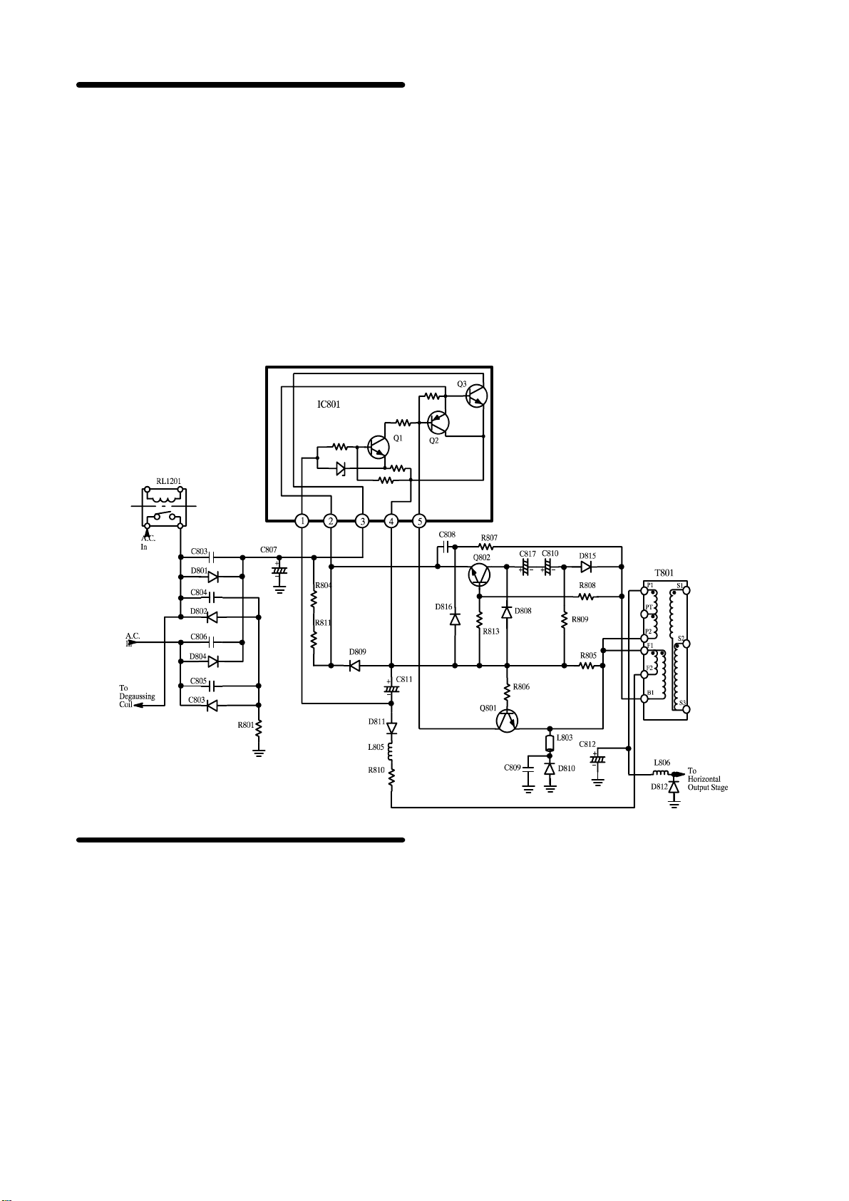
4.4. Protection
3DQDVRQLF
4.4.1.Overcurrent
The overcurrent protection circuit is made up of
resistor R805 and transistor Q801 which under
normal operating conditions is switched Off.
However in the case of a short circuit an excessive
current demand will be placed on internal transistor
Q3 which will result in an increased voltage drop
occurring across R805.
This increased voltage drop across R805 will result in
Q801 being biased into conduction, which in turn will
bias On internal transistor Q2 resulting in the base
bias of Q3 being removed. With no base bias on Q3
the output from pin 4 of IC801 is stopped.
The power supply will then initiate a repetitive rolling
cycle for the purpose of an automatic restart, if
necessary.
4.4.2.Overvoltage
The overvoltage protection circuit consists of zener
diode D812 which acts as a CROW BAR device.
This works by creating a short circuit resulting in the
overcurrent protection circuit described above being
activated.
4.5. Secondary Supply Side
On the secondary side, the supplies output from
transformer T801 are:
103V (14”) or 125V (21”) this supply which is fed from
winding P1 of T801 is used to supply the line output
stage.
22V is used to supply the audio output IC IC251
12V is used to produce the following additional
supplies:
: 9V supply produced by IC852 and supplies the
tuner and IC601
: 8V supply which is produced by IC853 is
used to supply IC201, IC601 and IC603.
: 5V supply produced by IC851 supplies
IC601 and IC602.
Finally all the above supplies are also monitored by
themicroprocessor IC1201 pin 31 for any short circuit
faults (described in
may occur.
If the microprocessor detects a short circuit fault at
pin 31 then the microprocessor switches the TV into
standby.
Microprocessor section
)which
Page 12
3DQDVRQLF
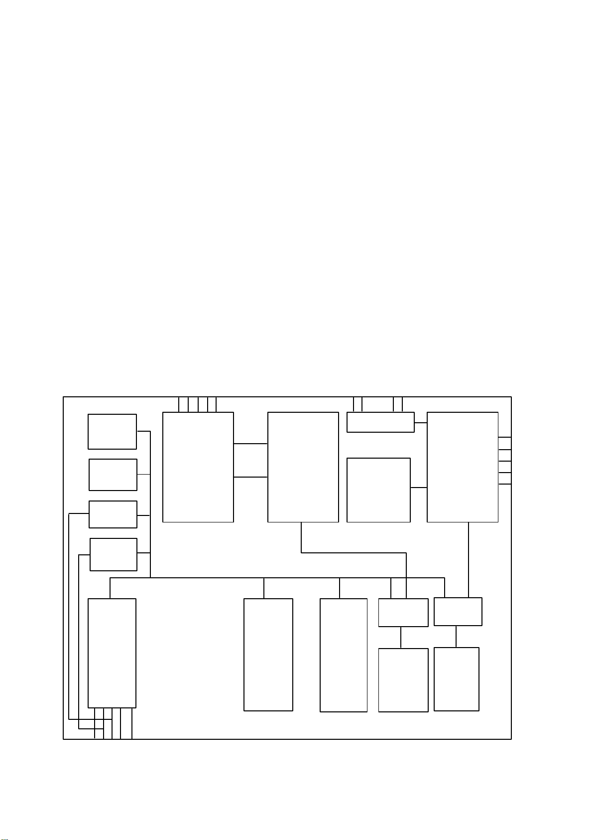
5. MICROPROCESSOR AND TELETEXT PROCESSING
The microprocessor SDA5254 used on Z7 teletext
models, not only performs the required control
processing but also teletext processing which is
incorporated in the microprocessor,theprocessingof
which will be looked at later. First the control
processing stageofthemicroprocessorwillbelooked
at.
The elements that the microprocessor requires to
perform the aforementioned functions are:
: 8 bit C500-CPU
: 18MHz internal clock
: Parallel 8-bit data and 16....19 bit address bus
: Eight 16 bit data pointer registers
: Two16bittimers
: Watch-dog timers
: Capture compare timer for infrared remote
control decoding
: Serial Interface
),/
),/
),/
&9%6
,5()
: 256 bytes on-chip RAM
: 8kbytes on-chip display RAM
: 1 kbyte on-chip ACQ-buffer-RAM
: 1 kbyte on-chip extended-RAM
: 6 channel 8 bit pulse Width Modulator
: 2 channel 14 bit Pulse Width Modulator
: 4 multiplexed ADC inputs with 8 bit resolution
: One 8 bit In/Out port with open drain and
2
operational I
C bus emulation
: Two 8 bit pulse mutifunctional In/Out ports
: One 4 bit port works as either digital or
analogue input
: One two bit In/Out port with optional functions
: One 3 bit In/Out port with optional RAM/ROM
address expansion up to 512Kbyte
/&,1
/&287
96
+66&
&DSWXUH
&RPSDUH
7LPHU
:DWFKGRJ
7LPHU
$'&
3:0
&38
77; 936
6OLFHU
77&
77'
([WHQGHG
'DWD
5$0
. %\WH
$FTXLVLWLRQ
'LVSOD\
3URJUDP
0HPRU\
520
7LPLQJ
&KDUDFWHU
520
'XDO 3RUW
,QWHUIDFH
%XIIHU
'LVSOD\
*HQHUDWRU
'XDO 3RUW
,QWHUIDFH
'LVSOD\
5$0
5
*
%
%ODQ
&RU
3
3
3
3
;7$/
;7$/
Page 13

3DQDVRQLF
5.1. Microprocessor Stage
Input Information
: Pins 5 - 9 - Local Keys
The local key commands are fed to the
microprocessor via pins 5, 6, 7, 8 and 9. These input
pins when not in use are held High via pull-up
resistors which are connected to the 5V standby
supply.
: Pins 12/13 - XTAL1 / XTAL2
Theinternaloscillatorofthe CPU issynchronised with
an external 18MHz quartz crystal X1201 which is
connected to pins 12 and 13.
TheClockfrequenciesfortheI
obtained from this frequency by internal dividing.
: Pin 15 - Reset
During power On/Off operation, or during a fall in
voltage to the microprocessor, incorrect operation
may occur. To prevent this incorrect operation the
microprocessor has a reset signal input via pin 15.
This reset signal is provided by reset IC IC1202 pin
1 which keeps the microprocessor in a stable
condition until the voltage level has risen and has
become stabilised.
This reset IC which is fed a5Vstandbysupply isinput
viapin2ofIC1202. At switch On this supply is less
than 4.3V which results in the reset IC pulling pin 15
of the microprocessor Low keeping the
microprocessor in a stable condition until the supply
voltage becomes greater than 4.3V at which time the
reset line goes High and the microprocessor begins
to operate.
: Pin 19 - AGC Detection
This input signal which fed via buffer transistor Q23
is used only for U.K. models to detect the strongest
signals during auto tuning.
: Pin 30 - CVBS
This composite video signal which is input via pin 30
is used for teletext processing which is carried out
within the microprocessor.
: Pin 31 - Short Circuit Protection
Pin 31 of the microprocessor which is normally held
High via R1218 is used to monitor the voltage supply
linesforshortcircuitfaults.Thesupplylineswhichare
monitored are:
: 33V supply which is also monitored via R1218
: 22V supply is monitored by transistors Q252
and Q253, which under normal operating
conditions are switched OFF.
: 12V supply monitored via D857
: 9V supply monitored via D858
: 8V supply monitored via D860
: 5V supply monitored via D859
: TheverticaloutputisprotectedbyQ453/Q454
2
Cbussystem arealso
the operation of this circuit being described in
section 11.1.
Ifafaultoccursresultinginoneoftheaforementioned
supplies failing then pin 31 of the microprocessor
would become Low resulting in the TV being shut
down into standby by the microprocessor.
: Pin 32 - ABL (Automatic Beam Current
Limiter)
The ABL input (pin 32 of the microprocessor) is used
toswitchtheTVintostandby in theeventofexcessive
beam current.
When the TV is operating normally then any increase
in beam current is regulated by the Video Processing
IC IC601 pin 26, which is discussed in the
Processing section
held High via a pull-up resistor R1220 and the
protection circuit does not operate.
Where a fault occurs and thebeam current continues
to increase and exceeds the control of IC601,the
zener diode D506 would conduct as its anode would
become more negative with respect to its cathode,
due to the negative voltages being fed back from
T552 (Flyback Transformer). As a result of D506
conducting pin 32 of the microprocessor would be
pulled Low, this would result in the TV then being
switched into standby.
: Pin 33 - AFC
During search mode the microprocessor detects the
AFC voltage input via pin 33, which is fed from pin 1
of IC601 via Q102.
WhentheAFCvoltagereachesmidlevelbetweenthe
highest and lowest points of its swing, the
microprocessor stops the searchoperation andholds
the data.
: Pin 36 - Power Good (PG)
This input terminal is used as a power OFF reset by
the microprocessor when the TV is switched into
standby. Without this power OFF reset the
microprocessor has no way of knowing that the TV
has been switched OFF into standby.
When the TV is switched OFF the operational data
from the video processing IC is lost, this means that
atswitchONthedatahastobereloadedbackintothe
video processing IC IC601.
To be able to do this the microprocessor has to be
reset so that at switch ON from standby the
microprocessor knows that it has to reload the
required data.
: Pin44-RemoteIN
ThecommandsrequiredforcontroloftheTVreceiver
are applied from the remote control.
The command from the remote control transmitter is
applied via RPM-637CBRS (remote control receiver)
and Q1212 topin44ofIC1201, this command data
being in serial format.
. Pin 32 of the microprocessor is
Video
Page 14

3DQDVRQLF
: Pin 45 - Sandcastle IN
This input is used by the microprocessor forclamping
and synchronisation of the CVBS signal used for
teletext processing and display.
: Pin 46 - Slow Switching
Pin 46 of the microprocessor is used to automatically
switch the TV to the 21 pin scart input terminal. This
is achieved by a high level being applied via pin 8 of
the 21 pin scart terminal which results in transistor
Q1240 conducting pulling pin 46 of the
microprocessor LOW. When this LOW level is
removedfrompin46theTVswitchesoutoftheabove
mentioned mode.
: Pin 52 - HFSW
This output is used for Interlace Suppression, when
in teletext mode pin 46 of the microprocessor
switches its output High or Low field by field. This
controllineisthenusedtoswitchtransistorQ1216On
and Off.
When Q1216 is conducting the junction at resistors
R451 and R453 is effectively grounded, shorting out
R453 causing the picture to shift vertically. This
results in the two fields being super imposed on the
top of each other preventing text jitter.
5.1.2.Output Information
: Pin 1 - Standby
This output port of the microprocessor is used to
control the switching of the TV in and out of standby.
This is achieved by controlling transistor Q1202.By
applying a High level to the base of Q1202 this
transistor conducts and causes transistor Q1203 to
switch Off preventing current flow via the winding of
standby relay RL1201, this causes the normal open
contact to open removing the mains A.C. supply from
mains power supply circuit. Likewise when a Low
level is fed to the base of Q1202 the transistor is
biased Off, thus allowing transistor Q1203 to conduct
by a High level which is applied via R1248. When
Q1203 conducts current via the standby relay
working coil causes the relay contact to close and
feeds the mains A.C. voltage to the power supply
circuit.
: Pin 4 - CATS Eye
Pins 4 of the microprocessor is used to control a
feature known as C.A.T.S. (C
racking System).
T
This is used to adjust the contrast level depending on
the external light surrounding the TV. The level of
adjustment made being dependant upon the mode
selected (either Medium / Maximum).
The light sensed by the LDR (Light Dependant
Resistor) R1223 is used to control the conduction of
transistor Q1217 which in in turn controls the voltage
level at pin 26 of IC601 and thus the contrast level is
adjusted accordingly.
ontrast Automatic
: Pin16-CATSOn/Off
The CATS Eye function described above can be
switched Off by the user if they so wish via the OSD.
The microprocessor pin 16 is responsible for this
control.
: Pin 20 - Off / Text
This output control line is used on teletext models
only. Here pin 20 of the microprocessor is fed to the
base of transistor Q1214 where the control line splits
into two paths, the second path we will look at shortly.
The control line fed to the circuit made up of
transistors Q1214 and Q1213 is used to control the
contrast level during Text operations
During non teletext operations pin 20 of the
microprocessor is LOW, this results in Q1214
conducting placing resistors R1290 and R1291 in
parallelwhich sets the base biasofQ1213 and in turn
the base bias of transistors Q1207, Q1208, Q1209
and setting the contrast level of the main picture and
OSD displays.
During teletext operations pin 20 of the
microprocessor goes HIGH this results in transistor
Q1214 being switched Off removing R1290 out of the
parallel configuration with R1291. This changes the
base bias of Q1213 and the base bias of Q1207,
Q1208 and Q1209. The result of this is to decrease
the contrast level for teletext viewing.
The second path that was mentioned earlier sees the
control line from pin 20 of the microprocessor being
fedfromthebaseofQ1214 to the base of transistor
Q1295. Transistor Q1295 along with Q1296 are used
to control the through put of the RGB signals from the
21pinscartsocketviatransistors Q3105, Q3106 and
Q3107 to IC601.
During non-teletex operation aLOW level from pin 20
ofthemicroprocessor is appliedtothebase ofQ1295
causing the transistor to conduct. When Q1295
conducts a Highlevelis appliedto thebase ofQ1296,
this biases Q1296 into conduction pulling the bases
of transistors Q3105, Q3106 and Q3107 LOW.
This LOW level which is appliedto these 3 transistors
biasesthemintoconductionallowingthe RGB signals
to be fed to IC601 for further processing.
In teletext operation pin 20 of the microprocessor is
HIGH. This HIGH level switches OFF Q1295 and in
turnQ1296resultinginaHIGHlevelbeingappliedvia
R1296tothebaseofthe3transistors Q3105, Q3106,
Q3107 forcing them into a non-conductive state.
When the 3 transistors are in a non-conductive state
the RGB signals from the 21 pin scart socket are
prevented from being applied to IC601, instead the
teletext RGB signal from the microprocessor is
applied to IC601.
Page 15

3DQDVRQLF
: Pin 21 - Coincidence Detection
This output from the microprocessor is used to
ensure that the OSD display remains stable when the
external sync. signal is poor or non-existent.
This is achieved by pin 21 of the microprocessor
outputing a High level to the base of Q303 which
results in the Horizontal oscillator circuit of IC601 pin
15 being modified by the addition of the filter circuit
made up of C319 and R320 being added into circuit.
: Pin 22 - Message Received
This output port, pin 22, is used to signal the user
when the TV has received a remote control signal by
flashing the standby LED.
Themicroprocessorviapin22outputs a pulsedsignal
whichisusedtoswitchtransistorQ1201 On and Off
causing the standby LED to flash.
: Pin 23 - Mute 2
The mute2 control line which is output from the
microprocessor pin 23 is fed to the audio output IC,
IC251 pin 25, via transistor Q251.
Duringchannelchange,tuning andmutingoperations
a high level is output from pin 23 which causes Q251
to conduct, this results in pin 5 of IC251 being pulled
LOW resulting in the audio output being muted.
: Pins 25 to 27 - FLT1, 2, 3
FLT3 pin 25 is used for the phase shifting of the VPS
or teletext data.
FLT2 pin 26 PLL filter for VPS slicing.
FLT1 pin 27 PLL filter is used by the teletext slicer.
: Pin 29 - IREF
This is a reference current output used by the vertical
output stage of IC601.
: Pins38/39-VideoClock(V.CLK)
These connections are used to provide an external
display clock reference frequency used for text
processing.
: Pin 40 - Mute 1
The mute 1 control line output from pin 40 is used to
mute the audio output via the 21 pin scart socket.
The mute control line is fed via diode D1210 and
R3130 to the emitter of Q3104. From the collector of
Q3104 the mute control is applied to the base of the
muting transistor Q3103.
This mute control is used during channel change,
tuning and user mute operations.
: Pin 42 - F/AV
Pin 42 of the microprocessor is used on French
modelsonly. This control lineisfedtoswitchingIC201
pin 10, again only used in French Models, to switch
AM sound and sound input via the AV terminal. (see
section 14.5.
: Pin 41 Pos/Neg_SC1/SC2
Pin 41 of the microprocessor has two functions which
it can perform. The first of these functions being used
for those models which can process different sound
carriers (i.e. 6.0MHz, 5.5MHz), here the SC1 and
SC2 function would select either sound carrier 1 or 2.
The second function that pin 41 can perform is for
those models which are able to process SECAM L
signals. Here pin 41 of the microprocessor not only
controls the sound carrier selection but also the
standards selection carried out in the I.F. stage.
: Pin 43 L’/L
Pin 43 of the microprocessor is used to select
between the two types of SECAMstandards L/L’, this
control signal being fed via transistor Q22 to the I.F.
stage used on SECAM L models only.
: Pins 47 to 49 - RGB Output
The RGB signals output from the microprocessor are
used to display the required teletext (text models
only) and OSD information on screen. The RGB
signals being output from the following terminals:
Blue - pin 49, Green - pin 48, Red - pin 47
: Pin 50 - Blanking
The blanking pulse output from the microprocessor
pin 50 is used to provide the required switching
control for the teletext and OSD displays.
Data Bus Lines
: Pins2/3
The microprocessor communicates with the tuner,
EEPROM memory IC (IC1205) and Video Processor
IC601. Data on this bus line consists of serial data
(SDA) and clock signal (SCL). SDA being input and
output from pin 2 and the SCL being output from
pin 3.
)
Page 16
3DQDVRQLF
5.2. Teletext Processing Stage
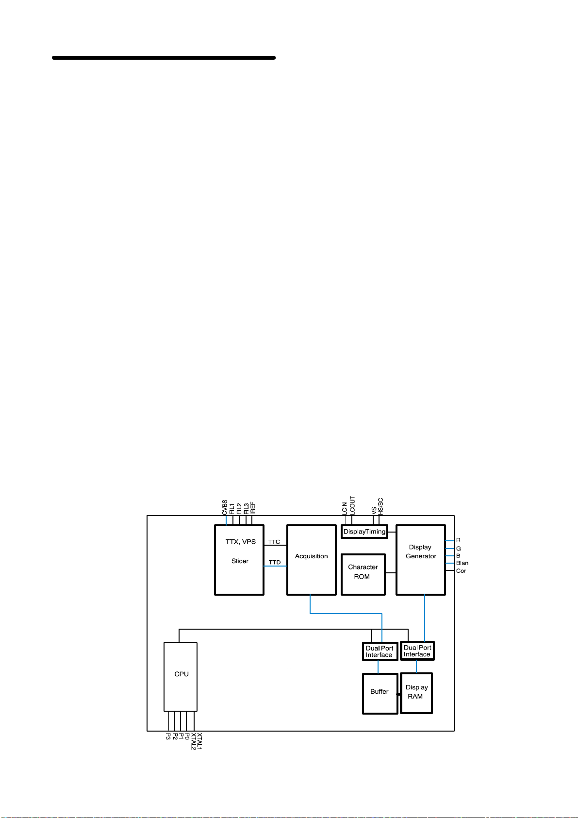
General
As already briefly mentioned earlier the
microprocessor performs teletext processing as well
asControlprocessing.Toperformteletextprocessing
the following elements are required:
: Teletext (TTX), Video Programme Signal
(VPS) slicer used to extract the relevant
information from the video signal.
: Acquisition stage allowing simultaneous
reception of both the Teletext(TTX) and Video
Programme Signal (VPS). The VPS feature is
not used.
: Display Timingwhichisused toensure that the
text information is locked to thesame timing as
the raster scan.
: Character ROM which provides the required
characters for display of text information on
screen
: Display Generator used to create the Text
display
5.2.1.Teletext Operation
To enable teletext processing by IC1201 a CVBS
signal is input via pin 30. Here the signal is fed to the
Teletext (TTX) slicer stage, where the horizontal and
vertical sync. information and TTX data are extracted
from the CVBS signal. To do this the slicer has an
analogcircuitforsync.filteringanddata slicing aswell
as an analog PLL used for system clock generation.
A third PLL is used to shift the system clock used for
data sampling of the TTX signal.
Output from the slicer stage the sliced bit stream is
fed to the Acquisition stage, where this bit stream is
converted into a byte stream and a framing code
check takes place to identify the TTX signal.
After framing code detection a status word is
generated which is used to identify the type of data
received and the signal quality of the TV channel.
The text data is then fed via the dual port interface to
the buffer , where under the control of the CPU the
data is stored in the display RAM until the TTX data
is required.
When the TTX data is requested the information is
read out of the Display RAM via the interface and fed
to the Display Generator.
The display generator then selects the pixel
information from the character ROM and translates it
into RGB values.
The character generator itself includes a character
and control decoder, a RAM interface, RGB and
Blanking signal generators.
To allow the character generator to carry out
processing of the TTX signal, generation of a pixel
clock is required.
This generation of the pixel clock is created internally
by the display timing stage which is fed a sandcastle
pulse input via pin 45.
TheTTXdatawhich has now been converted to RGB
valuesarethenoutputfrompins47(R),48(G),49(B)
with the blanking signal being output via pin 50.
These signals are then fed to the video processing IC
IC601 and are discussed in the
Video Processing
section.
Page 17

6. Memory (EEPROM)
3DQDVRQLF
The memory IC is interfaced with the microprocessor
via the I2C bus. The following data are memorised by
the memory IC.
Service Data
: Picture Geometry adjustments
: Model features (option bytes)
Tuning data for 60 programme positions
: Channel number
: SIF data SC1/SC2
: Colour system (PAL,SECAM or NTSC)
Last Memory Information
: Power on/off condition
: Programme position
: Volume level
: Colour level
: Contrast level
: Brightness level
: Sharpness level
: C-A-T-S mode
Page 18
3DQDVRQLF
7. COLOUR TV SIGNAL PROCESSING
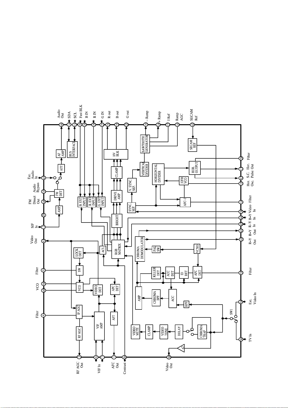
General
TV signal processing on Z7 is carried out by IC601
M52778SP.
This IC is responsible for the following processing:
: Composite video signal (Video input)
: Deflection Processing
: Video (V.I.F.)
: Sound (S.I.F.)
Each of the aforementioned processingblocks will be
looked at in turn.
Page 19
7.1. Video (V.I.F) Processing
3DQDVRQLF
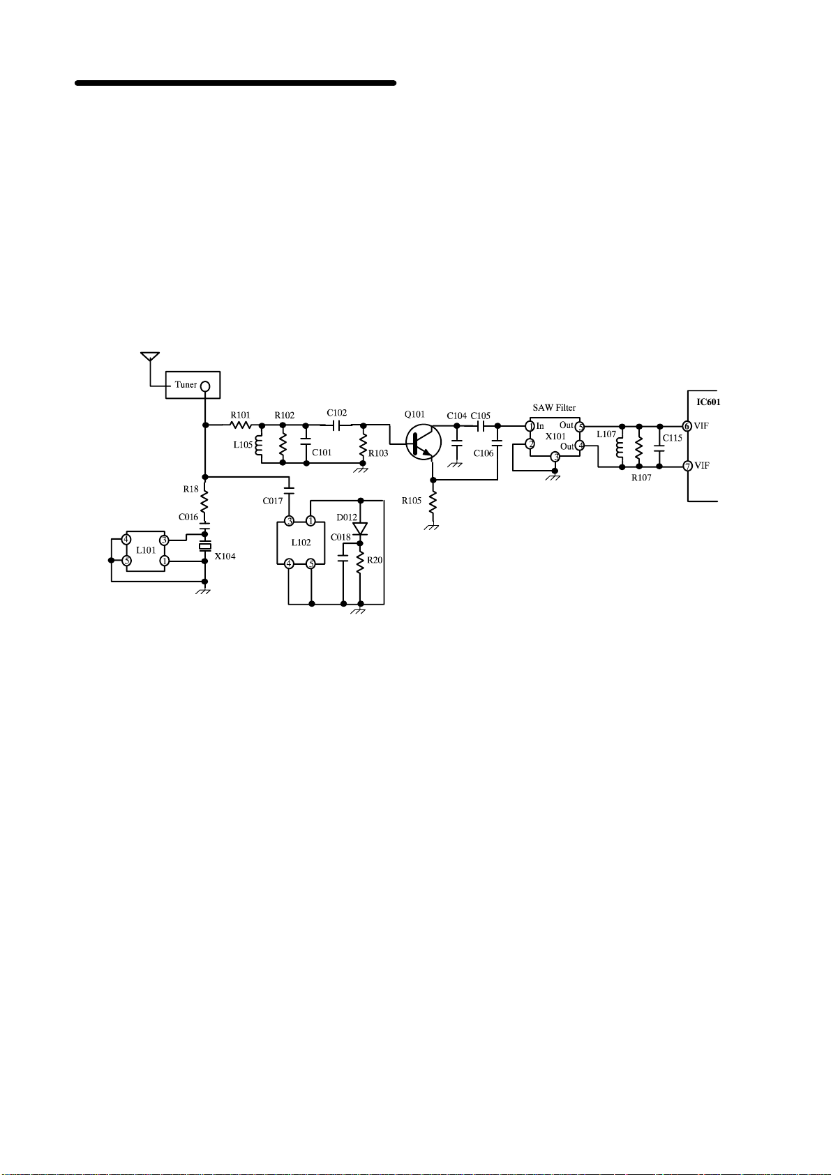
The I.F. signal required for V.I.F processing is fed
from the tuner, to pins 6 / 7 of IC601.
HoweverforSECAMLmodelsanadditional I.F.stage
is used. This stage is responsible for the processing
of the VIF and SIF signals which for all other models
are processed by the circuits described in the
following section (for the SECAM processing path
Appendices section 14.
see
The I.F. signal for PALprocessingis filtered via
L101 which is used as an adjacent channel trap ( n+1
processing).
).
Likewise for models with SECAM L and D/K
processing L102 is used for n+1 processing. Control
of this circuit being carried out by IC1201 pin 41,
which is fed to pin 1 of L102 adjusting the filtering
frequency depending on the standard being
processed.
The second path feeds the I.F. signal straight
to the SAW filter X101 pin 1 (or via Q101 where the
signal is buffered depending on the model). The
resulting V.I.Fsignalis then output via pins 4 and 5 of
X101, where the signal is input via pins 6 and 7 of
IC601.
The V.I.F signal input via pins 6 and 7 is amplified by
a VIF amplifier before being output to the following
processing stages. At the output of the VIF amplifier
the video signal is split into two paths.
The first path feeds the video signal to the AFT stage
which is used to monitor the I.F. signal frequency.
When the I.F. frequency is below 38.9MHz, the AFT
voltage at pin 1 of IC601 rises, this voltage is fed to
AFC terminal of the tuner which causes the I.F.
frequency to rise by controlling the tuner’s local
oscillator and maintaining the I.F. signal frequency at
38,9MHz. Likewise when the I.F. frequency is higher
than 38.9MHz the AFT voltage at pin 1 of IC601
reduces, again this voltage is fed to the AFC terminal
of the tuner which causes the I.F.frequency to fall by
controlling the tuners local oscillator and maintaining
the I.F. signal frequency at 38,9MHz.
This AFT voltage output via pin 1 of IC601 is also fed
to the microprocessor IC1201, which uses this
voltage during search mode. During search mode the
microprocessor detects the AFT voltage fed from pin
1ofIC601 and transistor Q102 topin33ofthe
microprocessor.
When the AFT voltage becomes mid level between
the highest and lowest points of its swing, the
microprocessor stops the search operation and
maintains the data.
The second path that the video signal takes within
IC601 is via the video detection stage, from here the
V.I.F. signal is fed to the VCO circuit whose reference
frequency is set via pins 49 and 50. At the output of
the VCO circuit a reference signal is fed back to the
video detection stage.
TheV.I.F. signal outputfromthevideodetectionstage
is also fed to the I.F. AGC stage whose filter circuit is
made up of C107 found at pin 4 of IC601 and used to
control the gain of the V.I.F. amplifier and keep the
correct signal output level.
TheI.F.AGCcircuitalsofeedsasignaltothe RF AGC
stage which outputs an AGC voltage via pin 3 of
IC601. The R.F. AGC circuit monitors the RF signal
for any increase in signal level above the I.F. AGC
rangeandcompensatesforthischangebycontrolling
the gain of the RF amplifier in the tuner.
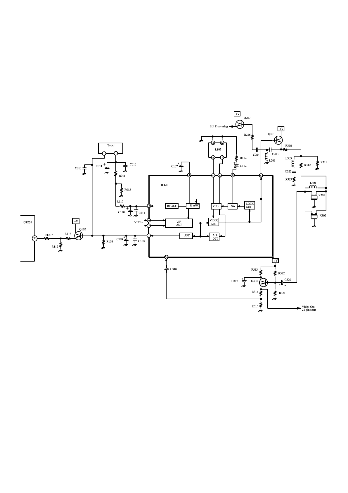
Finally the VIF signal is output from pin 52 of IC601
and fed via transistor Q301 where at its emitter the
signal splits into two paths, one for SIF processing
and the other for video processing.
Page 20
3DQDVRQLF
The signal which is to be used for SIF processing is
fed from the emitter of Q301 and applied to the base
of Q207. For video processing the signal again is fed
from the emitter of Q301 and is fed via resistor R310
wherethesignalisfedvia filters X301 and X302 tothe
base of transistor Q302.
At the base of transistor Q302 the video signal is fed
via the base-emitter junction where the video signal
is buffered, at the emitter of Q302 the video signal is
split into two paths once again.
The first of these paths sees the video signal being
fed via the 100W resistor R3111 to the base of Q3101
where the signal is buffered. At its emitter the video
signal is applied to the video out pin 19 of the 21 pin
scart socket.
The second path at the emitter of Q302 has the video
signal being fed via R314 (a 470W resistor) to the TV
input terminal pin 36 of IC601.
Page 21
3DQDVRQLF
7.2. Video Signal Processing
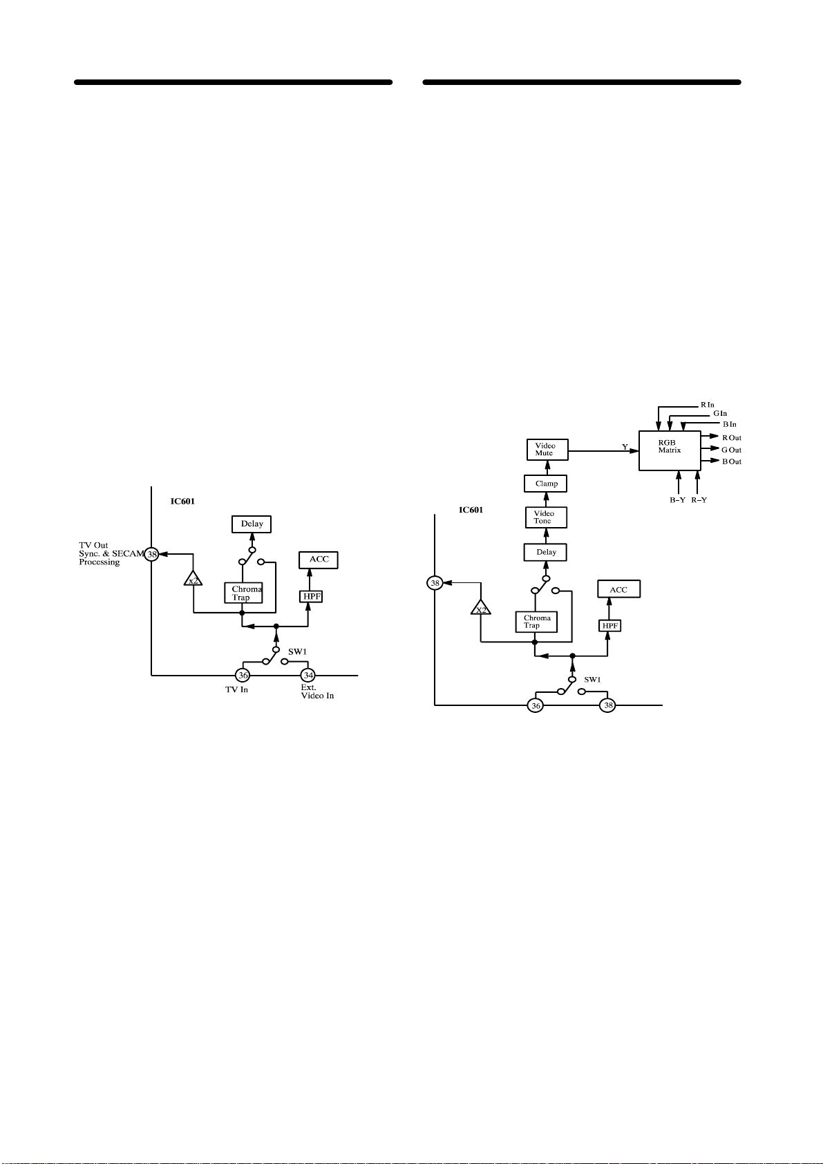
Thevideo signal which is applied to an internalswitch
of IC601 which is used to select between TV in pin 36
andanexternalvideosignalfed from the AVterminals
to pin 34. The selected video signal output from the
switch then follows two paths.
One path has the video signal being fed to the
Chroma trap for Luminance processing, while the
second path has the video signal being applied to the
High Pass Filter (HPF) stage for chroma processing.
The video signal which is fed to the luminance
processing path is applied to the chroma trap stage.
At the input of the chroma trap the video signal splits
into two paths.
The one path feeds the video signal via a x2 amplifier
wherethesignalisoutputvia pin 38, this signalisthen
fed for sync. processing, here the signal is inputback
to IC601 via pin 39, while for SECAM chroma
processing the video signal is input to IC603.
The second path feeds the video signal via the
chroma trap for luminance processing.
7.3. Luminance Processing
To process a PAL or SECAM luma signal, the video
signal is fed via the chroma trap which filters out the
chroma component from the video signal leaving only
the luma component at its output.
The luma signal is now fed to a delay line which
compensates for the processing time difference
between the the luma and chroma signals. From the
output of the delay line the next stage in the luma
processing path is the video tone circuit which is
sharpness processing. The amount of sharpness
appliedtothelumasignalbeingsetbytheuserviathe
OSD display.
Once the luma signal has undergone sharpness
processingthelumasignalisthenfed via a clamp and
video mute stage, before the signal is input to the
RGB matrix stage where the RGB signals are
produced.
Page 22
3DQDVRQLF
7.4. PAL Chrominance Processing
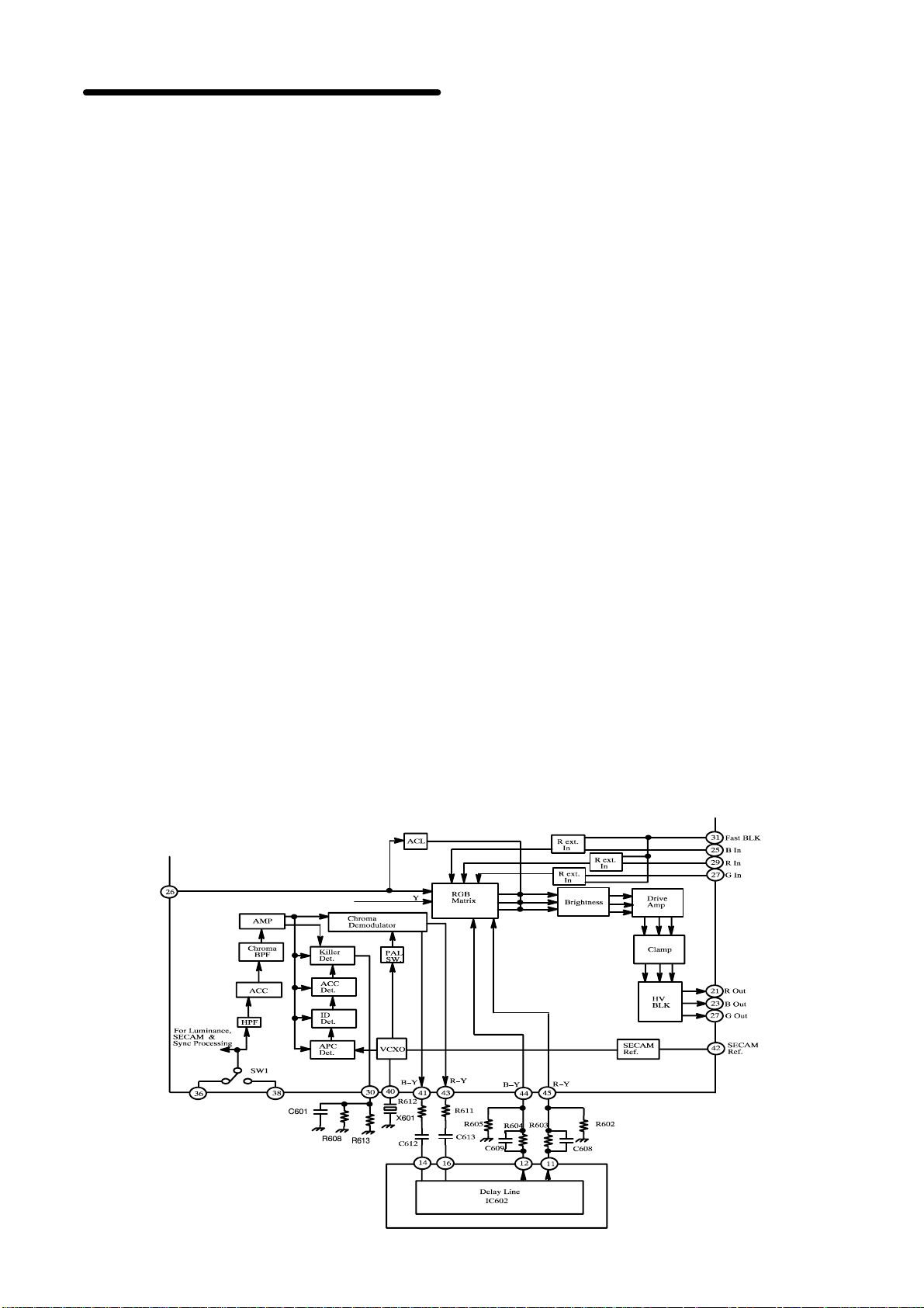
Tocarry out chroma processing the video signalisfed
viatheHighPassFilter(HPF) to the AutomaticColour
Control (ACC) controlled amplifier.Here the signal is
amplifiedandfed to the Band Pass Filter (BPF) which
is used to remove the luma component from the
chroma signal.
The chroma signal is then fed to a second amplifier
circuit, this being controlled by the colour killer
detection stage whose filter circuit consists of C601,
R608 and R613 which can be found at pin 30. The
chroma signal output from the second amplifier then
splits into two paths.
The first path feeds the chroma signal to the
demodulator stage which is controlled by the PAL
switch, here the differential R-Y and B-Y signals are
produced.
Thesecondpathfeedsthechromasignaltoanumber
of control stages. Here the colour burst is used as a
reference signal. The colour burst which is exacted
from the chroma signal is used as a control pulse for
the APC (Automatic Phase Control) circuit.
AlsofedtotheAPCstageistheVCOreferencesignal
of 4.43MHz which is set by X601 at pin 40.
In the APC stage (whose filter circuit you will find at
pin 35) the phase difference between the VCO
reference signal and the colour burst signal is
detected and output as a DC voltage.
This DC voltage controls the reference signal which
is applied to the demodulator stage.
During SECAM processing a reference signal is fed
from IC603 pin 1 to pin 42 of IC601. Here this signal
is fed to the VCO stage adjusting the crystal
controlled oscillator for SECAM processing.
The frequency of the burst is also used to identify the
current chroma carrier frequency which can then be
used for automatic standards detection which takes
place in the ID Detection stage, which then selects
the appropriate processing either PAL or SECAM.
The differential R-Y / B-Y signals output from the
demodulator are fed viapins 41 and 43 to IC602.The
differential R-Y / B-Y signals are input to IC602 via
pins 14 (R-Y) and 16 (B-Y). The signals are then
processed by this baseband delay line (discussed in
section8.
the
11 (R-Y) / 12 (B-Y) and fed back to IC601 via pins44
(B-Y) / 45 (R-Y) for further processing.
The R-Y / B-Y signals are then fed to the RGB matrix
stage from the output of which the RGB signals are
split in to two paths.
ThefirstpathfeedstheRGBsignalstotheBrightness
control stage. Here the amount of brightness applied
to the RGB signals is controlled by the user via the
OSD display.
The second path feeds the RGB signals to the
Automatic Contrast Limiting (ACL) stage. Here this
circuit is fed information from the CATSEyecircuitvia
Q1217 as well as information used to guard against
excessive beam current being drawn. Both input
information which is fed via pin 26 of IC601 is then
used to control the level of contrast.
Once the RGB signal is output from the brightness
control stage, the signals are applied to the Drive
amplifier stage where the red drive and green drive
are set. The red and green drives being set via
software control which can be set in service mode.
The next control stage in the video processing path
is the clamp stage which is used to set the Cut-off for
the RGB signals. Again the cut-off levels can be
adjusted in service mode. The RGB signals are then
fed via the HV blanking stage before the RGB signals
are output via pins 21 (R), 22 (G), 23 (B) and fed to
the Y-Board and displayed on the CRT.
) before the signals are output from pins
Page 23
7.5. SECAM Processing
3DQDVRQLF
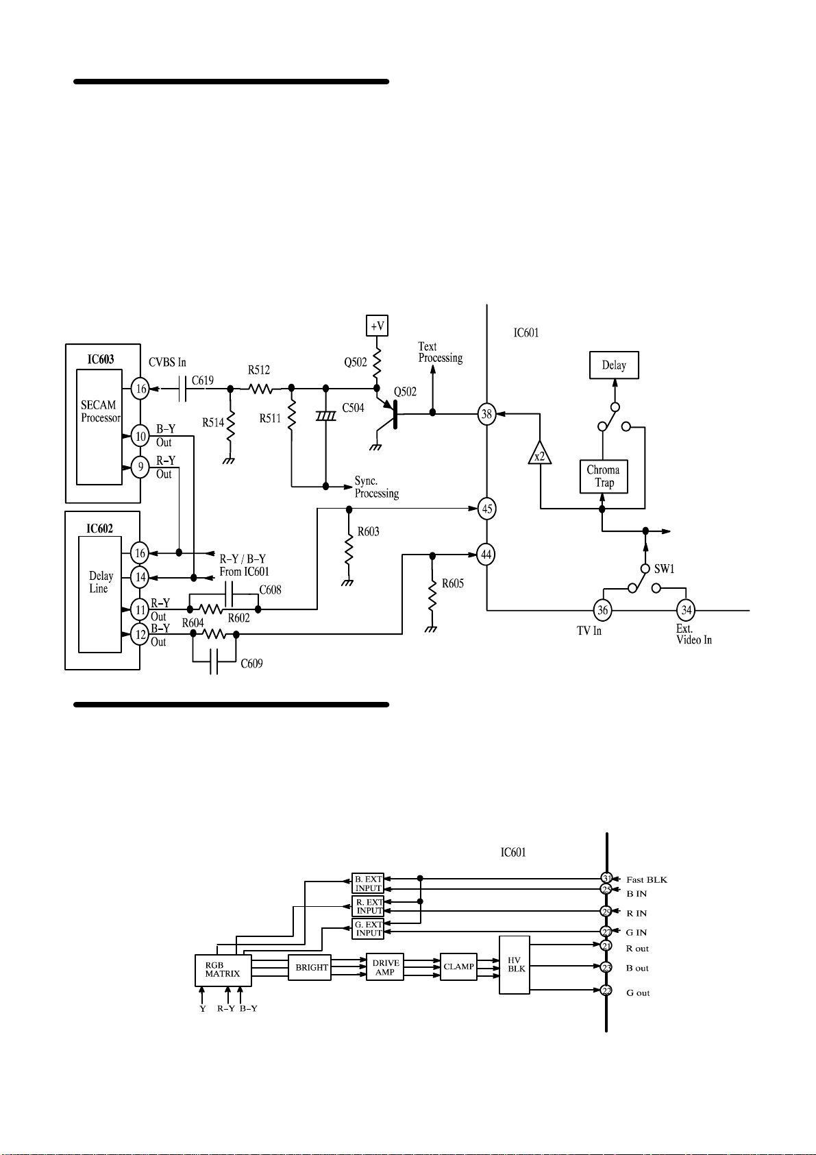
To carry out SECAM processing as mentioned
previously the video signal is output from pin 38 of
IC601 and fed via Q502 topin16ofIC603 which is
used to process the chroma component of the
SECAM video signal.
SECAM chroma processing IC IC603 will be looked
section 9.
at in
processed the differential R-Y / B-Y signals are then
outviapins9and10ofIC603.Thesesignals are then
fed to IC602 the baseband delay line IC where the
Once the chroma signal has been
signals are input via pins 14 and 16. Again the
processing of this IC is covered in a later section.
However the processed SECAM chroma signal then
follows the same path as mentioned in the previous
PAL chroma processing stage.
The luminance signal processing for SECAM is
carried out in the same way as previously described
in the PAL Luminance processing stage.
7.6. RGB Input
IC601 via pins 25, 27 and 29 allows external RGB
signals to be input along with a fast blanking pulse
inputviapin31whichisusedforswitchingtheinternal
RGB interface. These RGB signals can be fed from
either the Microprocessor IC1201 for display of
Teletext or OSD or from the 21 pin scart terminal.
These RGB signals are fed via the internal interface
to the RGB matrix, from here the external RGB
signals then follow the previously described
processing path.
Page 24
3DQDVRQLF
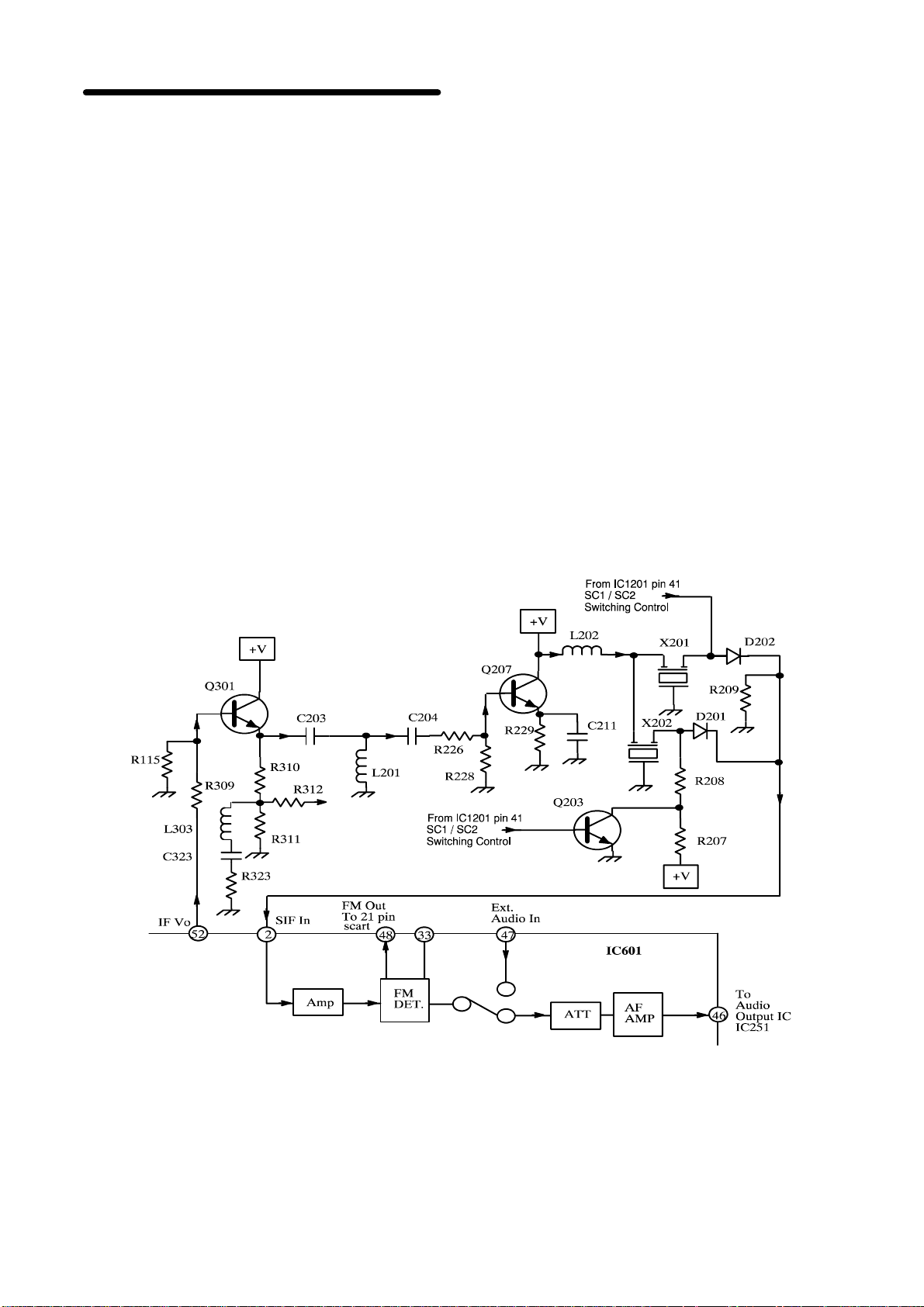
7.7. Audio Processing
The Colour TV Signal Processor IC601 is also
responsible for the processing of the audio signal.
To carry out audio processing the V.I.F . signal output
viapin52isfedas mentioned previously viatransistor
Q301 to the base of Q207. This V.I.F. signal is then
fed via the S.I.F. filters X201 (6MHz) or X202
(6.5MHz).
The selection between these S.I.F. filters is carried
out by the microprocessor pin 41 which is fed to
resistor R210. At R210 the control line splits into two
paths.
The first path sees the control line being fed via R210
to the anode of diode D202, while the second path of
the control line is fed via R212 to the base of Q203.
When the microprocessor pin 41 selects SC1 the
control line goes LOW. This low level results in D202
becoming non-conductive and Q203 being switched
OFF. With Q203 switched off diode D201 becomes
conductiveduetotheHIGHlevelfed via R207 /R208,
which allows X202 to be used for the required
processing.
Likewise when SC2 (6MHz) is selected the control
line becomes HIGH resulting in Q203 switching ON
and D201 being switched OFF. Diode D202 however
switches ON allowing filter X201 to be used for the
required processing.
This separated S.I.F. signal is then fed to pin 2 of
IC601 to the internal amplifier and FM detector
circuits. The FM detector circuit has two outputs.
The first of these outputs is via pin 48 of IC601,this
feeds the audio signal to the 21 pin scart socket pins
1 and 3 via transistors Q201 / Q202.
Thesecondpathfeedstheaudio signal via aninternal
switch which is used to switch between the internally
processed audio signal and an external audio signal
fed from the A Vterminals. The selected audio signal
is then fed to the following audio processing stage the
Attenuation (ATT) circuit, this stage being
responsible for setting the gain of the audio signal
before the signal is fed to AF amplifier. The audio
signal which is output from the amplifier stage is then
outputviapin46andfedtotheaudiooutputICIC251,
which will be described in
section 13.
Page 25
3DQDVRQLF
7.8. Deflection Processing
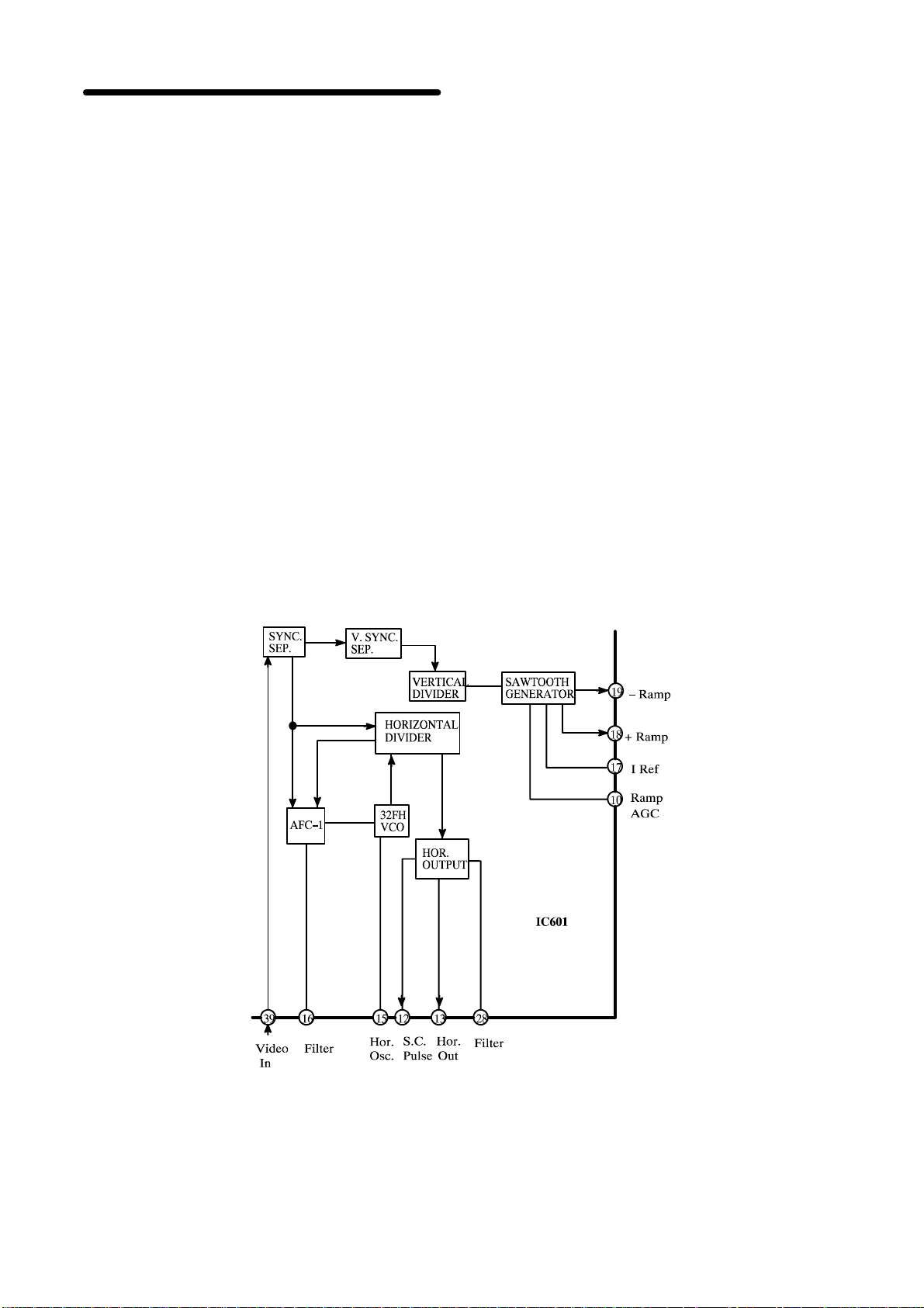
To carry out deflection processing the Luminance
signal is input via pin 39 of IC601 and is applied to the
internal sync. separator, here the sync separator
slices the middle of the sync. pulse. Once the sync.
signal has been separated the signal is output via
three paths to :
: Vertical sync. Separator
: Horizontal Divider
: AFC-1
7.8.1.Horizontal Processing
After the separation of the sync. signal, the signal is
fedtothe horizontal divider wherethe horizontal sync
pulse is produced.
The horizontal divider has two outputs which feed a
horizontal pulse to the horizontal output, via the first
path while the second path sees the horizontal sync
pulse being fed to the AFC-1 stage with its relevant
filtercomponentsbeingconnected at pin 16. Here the
horizontal sync pulse and the sync signal from the
sync separator are compared, the result of which are
used to control the VCO circuit whose crystal
oscillator X303 is connected to pin 15. The VCO
stage being used to control the horizontal drive pulse
allowing synchronisation of the horizontal sync
signal.
The horizontal sync signal is then fed via the
horizontal output stage, where the horizontal drive
pulse is output from IC601 via pin 13.
The timing for the output of the horizontal drive pulse
is derived from the heater supply of the flyback
transformer T552, this horizontal flyback pulse is fed
via a timing circuit to the base of Q503 before being
fed via Q504 and pin 12 of IC601 which has two
functions.
The horizontal flyback pulse input via pin 12 of IC601
is then also used to produce the sandcastle pulse
which is also output via pin 12 of IC601.
7.8.2.Vertical Processing
The sync. pulse output from the sync. separator is
also fed to the Vertical Sync. Separator. After which
thesignalisfed to theverticaldividerwhichcountsthe
horizontal pulses fed from the oscillator used for line
drive circuits.
When the divider receives a vertical sync. signalfrom
the vertical sync. separator itoutputs a drive pulse to
the ramp generator stage. From the ramp generator
a differential drive pulse is output via pins 18 and 19
and fed to the vertical output IC IC451.
Page 26
3DQDVRQLF
8. BASEBAND DELAY LINE
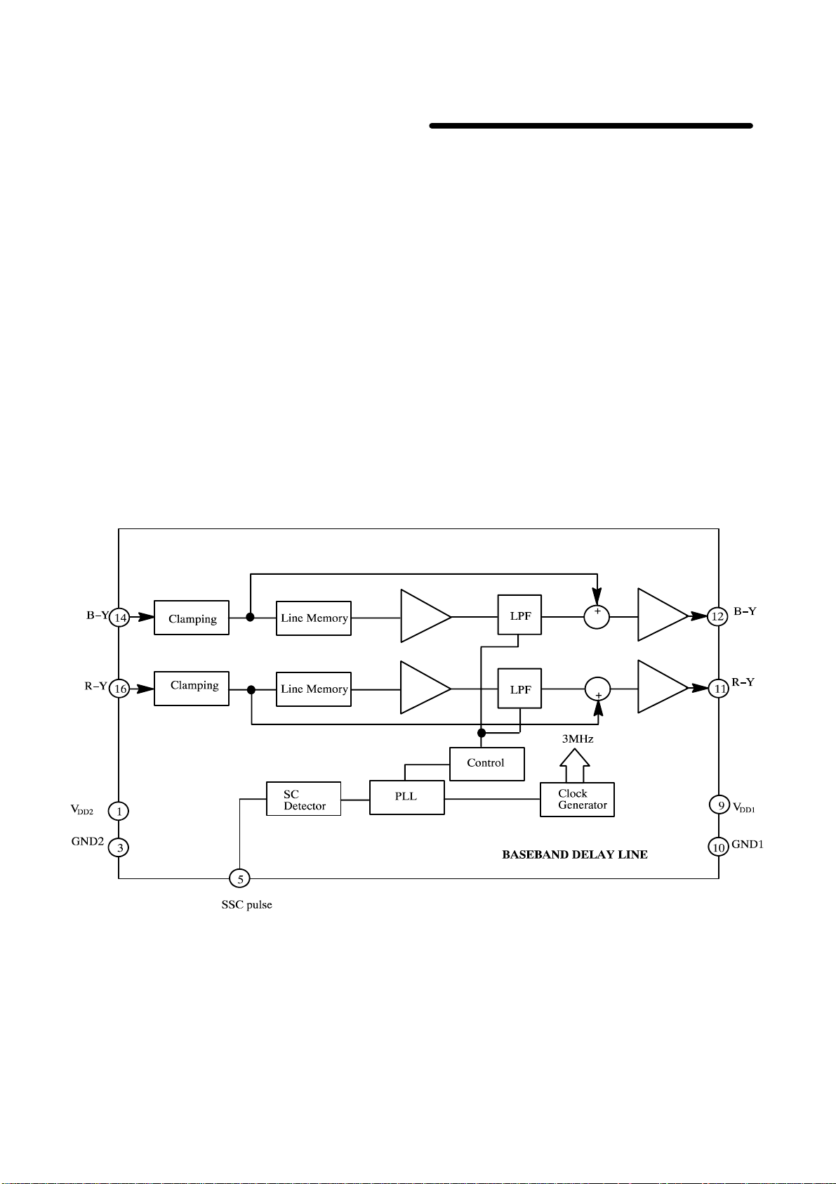
TheintegratedDelayLineIC,IC602U3665M,isused
for the processing of colour difference signals. To
carry out this processing the IC has the following
features:
Features
: One line delay time, addition of delayed and
non-delayed output signals.
: Adjustment free application and VCO without
external components
: Processes both negative and positive colour
difference input signals
: Clamping of A.C. coupled input signals [p
(R-Y) and p (B-Y) ]
: Line-Locked by the sandcastle pulse
: No crosstalk between SECAM
colour-difference signals
: Correction of phase errors in the PAL system
8.1. Operation
The colour difference signals enter IC602 via pins 14
(B-Y) and 16 (R-Y), where the signals are fed via 2
clamping circuits (one in each path). At the output of
the clamping stages the signals split into two paths.
: The first path feeds a non-delayed signal
directly to the input of the adder circuit.
: The second path feeds the signal to the line
memory, this signal is then delayed.
The signals output from the line memory are then fed
via a buffer stage to a low pass filter before they are
input into the adder stage.
The adder circuit then corrects for phase errors and
provides signal outputs at pins 11 and 12 of IC602.
Synchronisation of internal processing of IC602 is
provided by the sandcastle pulse input via pin 5 of
IC602.
As IC602 consists of digital and analogue stages two
+5V supplies are fed to pin 1 (digital supply) and pin
9 (analogue supply).
Page 27
9. SECAM CHROMINANCE PROCESSOR
3DQDVRQLF
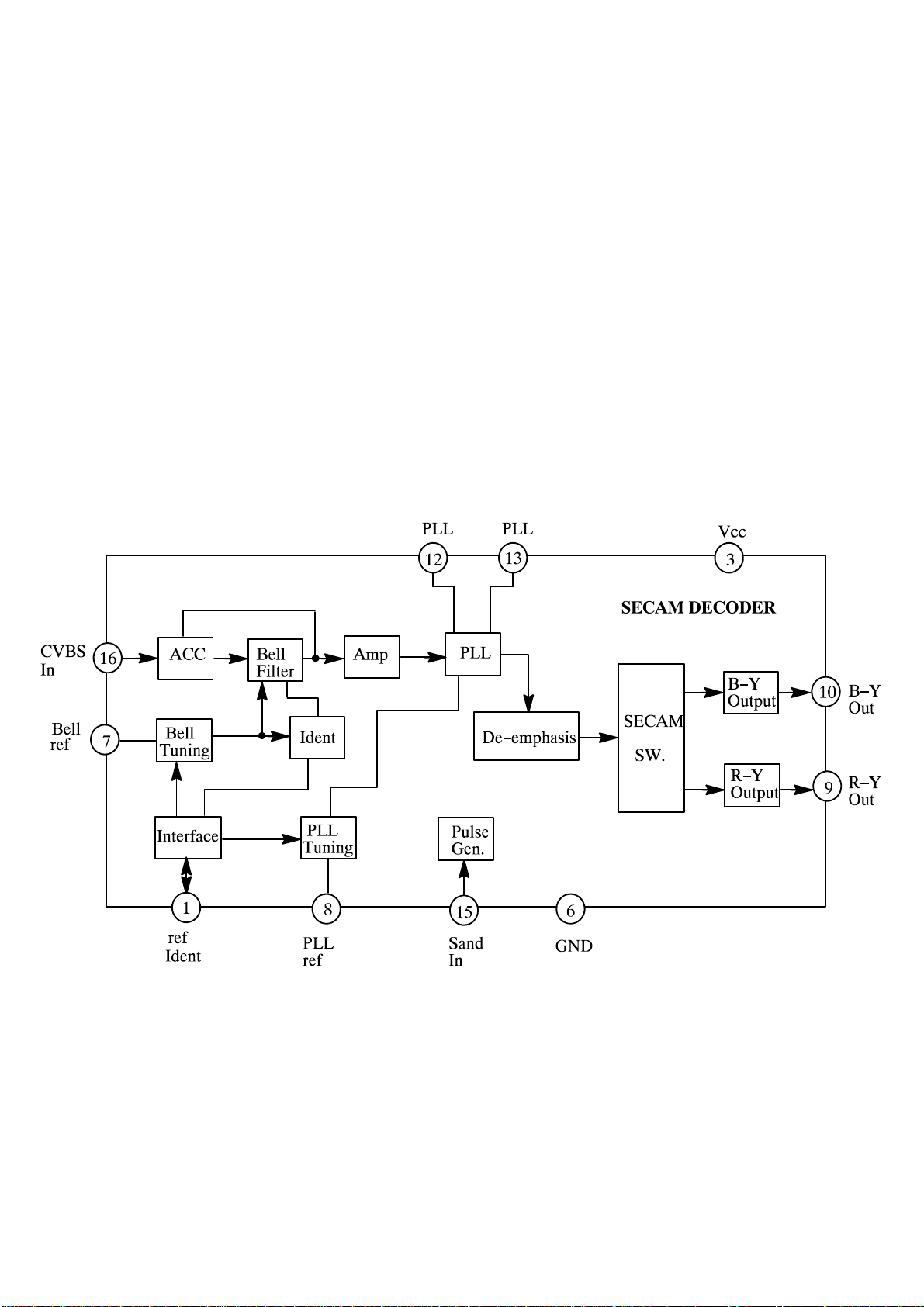
IC603 M52325AP is designed for SECAM
chrominance processing, for which the following
stages are required.
: Bell Filter
: Demodulator
: Indentification stage
The CVBS signal for SECAM chroma signal
processing as mentioned in the previous section is
output from IC601 pin 38, where the signal is fed via
transistor Q502 topin16ofIC603.
The CVBS signal input via pin 16 is then fed via the
Automatic Colour Control (ACC) stage which feeds
the signal to the following Bell filter circuit, here the
luminance component is removed from the chroma
component.
Attheoutput of the Bell filter the chroma signal is then
fedtoanamplifier stage beforethesignalisfed via the
PLL stage. Control of the PLL stage being carried out
by the PLL tuning stage whose reference is set by
C615 at pin 8.
The chroma signal from the bell filter is also fed to the
Ident stage which is used to detect a SECAM chroma
signal the result of which is fed via pin 1 of IC603 and
used to control the internal VCO stage of IC601.
The SECAM chroma which is output from the PLL
stage is then fed to the De-emphasis stage where the
transmitted pre-emphasis of the upper frequencies
are cancelled. The chroma signal is then fed via the
following SECAM switch before the R-Y and B-Y
signals are fed via the output interface to pin 9 (R-Y)
and pin 10 (B-Y).
These colour difference signals are then applied to
the delay line IC IC602, where the same path as
described for the PAL signals are followed.
Page 28
3DQDVRQLF
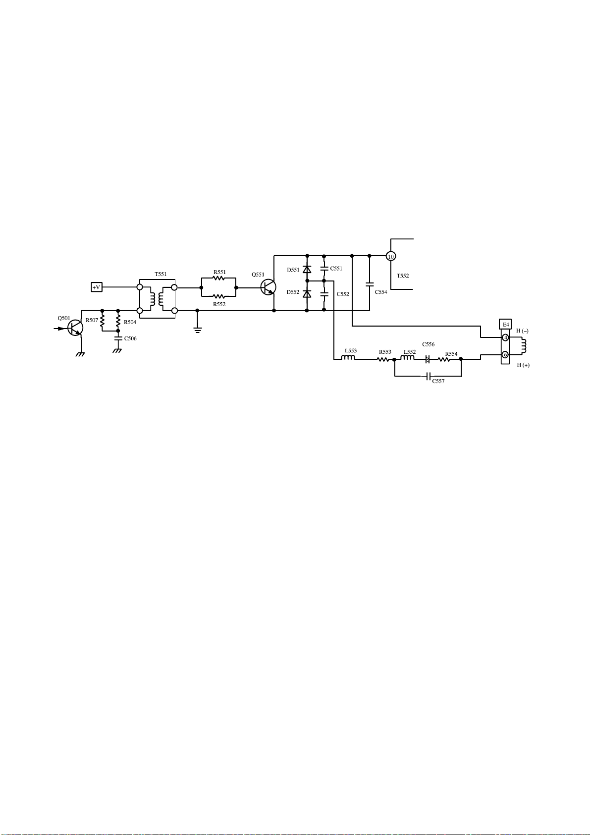
10. HORIZONTAL OUTPUT
The line drive signal from pin 13 of IC601 is fed to the
horizontal drive transistor Q501. This transistor has
a transformer T551 in its collector circuit, which is
used to provide A.C. coupling and impedance
matching with the horizontal output transistor Q551.
To ensure that transistor Q501 is not damaged by
excessive spikesgenerated by back EMFin the drive
transformer, a filter network R504, R507 and C506
are connected across the emitter collector of the
transistor.
The horizontal output transistor Q551 is used to drive
the horizontal deflection coils and flyback
transformer.
Linearity is achieved by the group of components
which consist of R554, C557, C556, L552 (R553,
L553 depending on model) and the diode modulators
in the form of D551 and D552.
The horizontal output stage provides deflection
current for the scan coils, EHT for the CRT and a
number of supply lines for peripheral circuits.
Page 29
11. VERTICAL OUTPUT
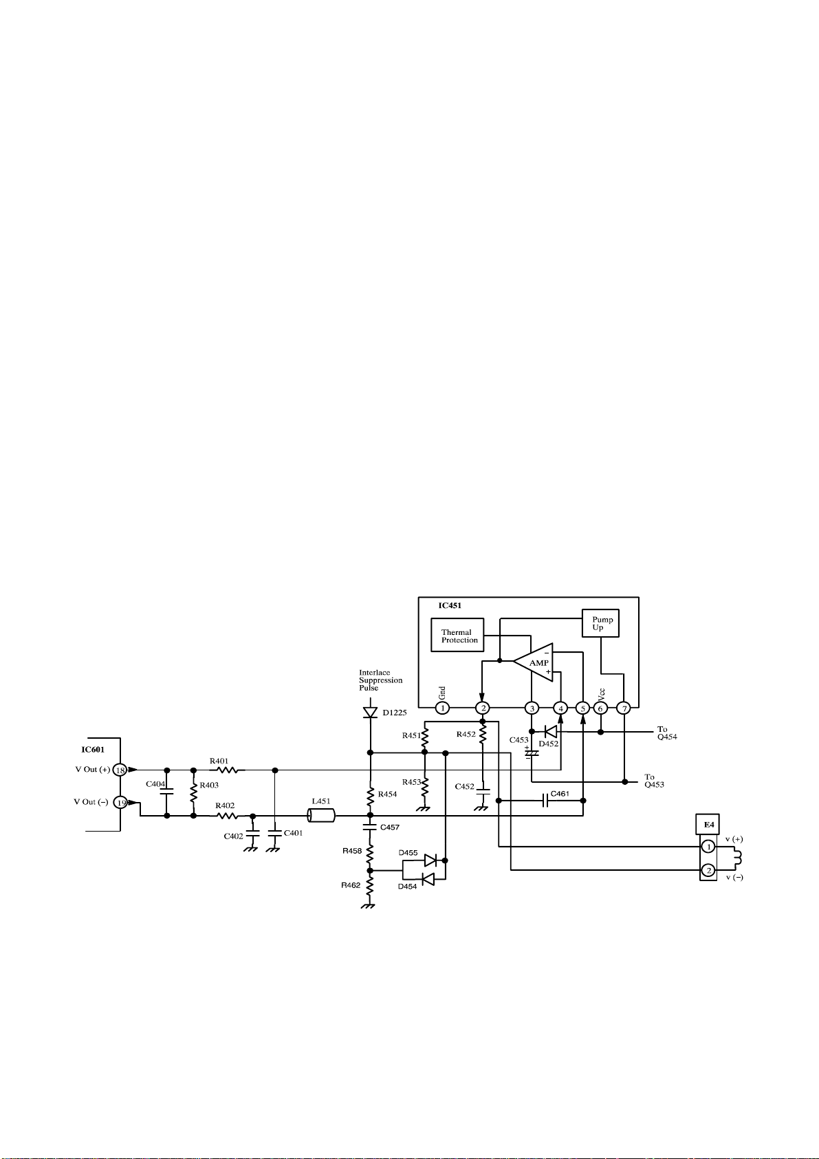
The vertical timebase functions are provided in two
parts, IC601 which produces the synchronisation,
vertical oscillation and control, while the vertical drive
for the deflection coils is provided by IC451.
The vertical drive signal outputs (Vout[-]and Vout[+])
are fed from IC601 pins 18 and 19, these outputs
forminga differentialoutput current which is fed to the
vertical output IC IC451 pins 4 and 5. At the output of
of IC601 a resistor R403 is connected between the
input pins of IC451. Resistor R403 being responsible
for determining the output current through the
deflection coil.
This vertical output IC IC451 which consists of an
operational amplifier to which the pre-amplified
sawtooth waveform is passed, results in a vertical
drive pulse being output via pin 2 of IC451. The gain
of the internal op-amp being controlled by the
negative feedback pulse which is fed via R454
connected between pin 2 and pin 5.
The Vertical drive pulse output from pin 2 of IC451
then undergoes linearity correction which is
performed by C457, R458 and R462. S-Correction is
performed by diodes D455 and D454.
3DQDVRQLF
IC451 also contains a Pump Up circuit which is used
to provide a switching voltage for the vertical flyback
period.
This is required as the energy requirement of the
vertical output stage is highest during flyback, as the
electron beam has to be passed rapidly from the
bottom right hand corner of the screen to the top left
corner of the screen.
This brief additional energy requirement is met by
doubling the supply voltage available to the vertical
output stage.
During vertical sweep, the bootstrap capacitor C453
is charged up to almost supply voltage via D452. The
outputofthe pump up generator pin 7, IC451 is at this
moment at ground potential.
As a result of the DC. displacement at the negative
pole of capacitor C452 (rising to the supply voltage),
build up of the supply voltage for the output stage at
pin 3 rises to almost twice the supply voltage. At the
same time, D452 is reverse biasedand thus prevents
discharge of C563 into the supply line.
Page 30
3DQDVRQLF
11.1. Vertical Protection
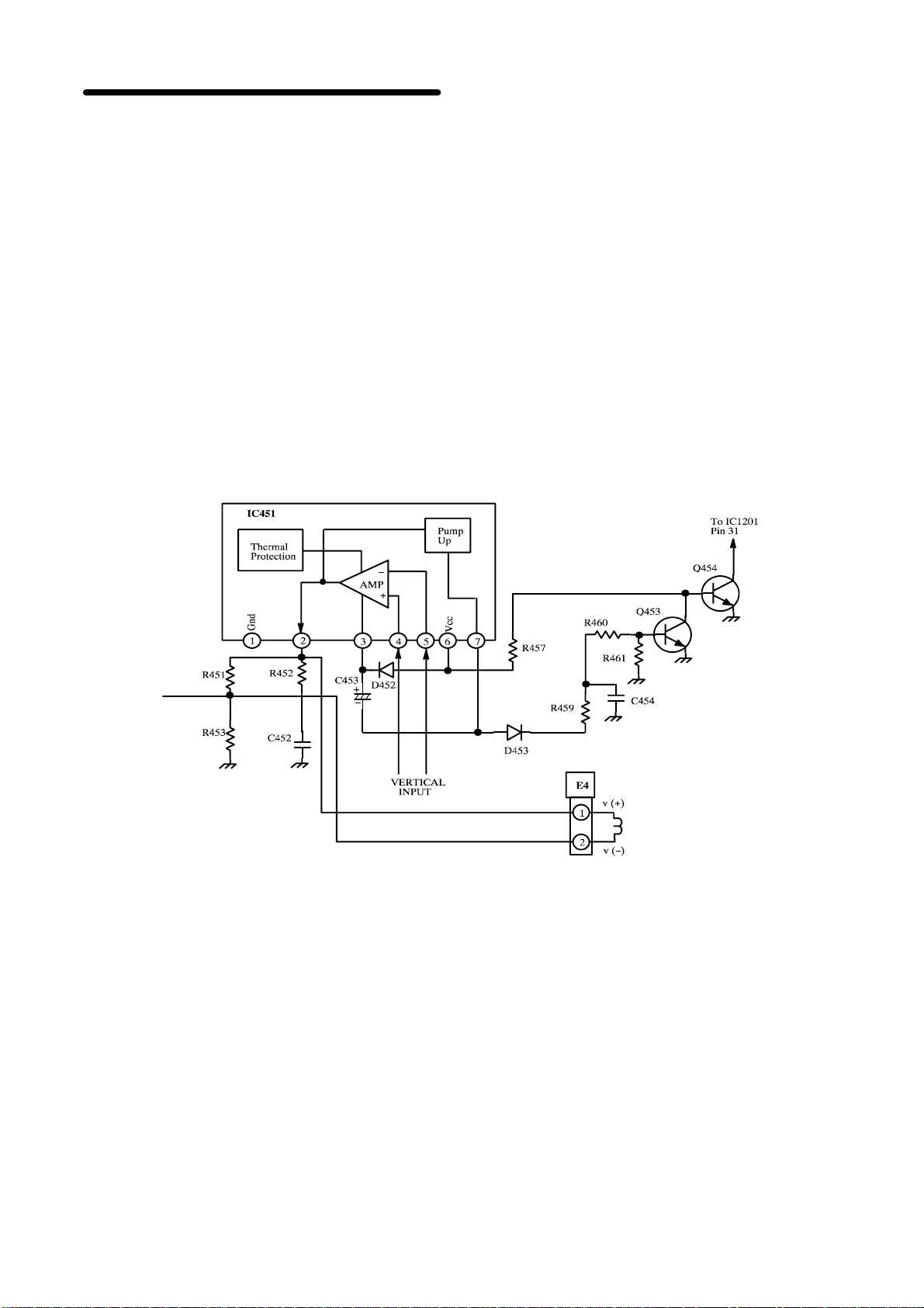
Theoutputpin,pin2 which is directly connected tothe
deflection coil is short circuit proof, the protection
circuit for which is made up of Q453 and Q454
monitors the state of the vertical output and feeds the
result back to the microprocessor pin 31.
During normal operation Q453 is baised ON by the
switching voltage output from pin 7 of IC451. When
Q453 is conducting transistor Q454 is switched OFF
resulting in pin 31 of the microprocessor remaining
High, this High level being fed via R1217 / R1218.
This High level which is applied to pin 31 of the
microprocessor ensures that the protection circuit
does not operate.
In the event of a vertical output failure the base bias
of Q453 falls resulting in Q453 switching OFF. When
Q453 switches OFF Q454 is biased ON by a High
levelfedviaR457.With Q454conductingpin31ofthe
microprocessor is pulled Low.
After a short delay, the microprocessor switches the
TV into standby.
As well as the safety circuit just described the output
pin, pin 2 of IC451 is also thermally protected by an
internal thermal protection stage.
This thermal protection stage is used to respond to
temperature change and limit the driving currents so
that no further temperature rise can occur, this
ensures that the output stage can only be operated
within the permissible operating range.
Page 31

12. BEAM CURRENT LIMITING (A.B.L.)
3DQDVRQLF
The C.R.T. beam current is monitored from pin 4 of
the flyback transformer T552. As the beam current
increases, an increasingly negative charge is
developed across C558.
This negative charge which is developed across
C558 is fed to the base of transistor Q507.
Transistor Q507 is used to maintain the setting of the
height with respect to the change in contrast. This is
because as the contrast increases, the height will
decrease and vise versa.
To compensate for this, transistor Q507 is switched
OFF by the negative voltage that is fed back from pin
4 of flyback transformer T552 as the contrast
increases. By switching OFF Q507 the height will be
maintained at its original setting instead of reducing.
Likes wise if the contrast is reduced Q507 is switched
ON and instead of the height increasing it remains
stable.
This negative charge is also passed to pin 26 the
contrast control input of IC601 used to limit the beam
current.
The negative charge which increases across C558 is
passed via resistor R519 and D503. This has the
effect of reducing the positive voltage being applied
to the contrast control of IC601 pin 26 which in turn
reduces the beam current.
If however the beam current continues to increase to
a point where it reaches approx. 1.1mA, the
maximum control range of the F.B.T. pin 4 will be
reached. At this point D506 will conduct causing pin
32 of the microprossor to go LOW.
After a short delay the TV will be switched into
standby.
Page 32
3DQDVRQLF
13. A.F. OUTPUT STAGE
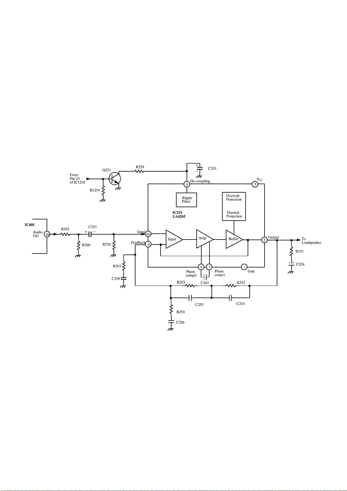
The amplitude controlled AF signal is output from pin
46 of IC601. The audio signal is fed directly to the
audio output IC IC251 via a de-coupling capacitor
C252. The audio signal is then input via pin 10 of
IC251 where the signal is amplified and output via pin
2. The audio signal is then fed to the loudspeaker via
the headphone socket.
The usual negative feedback occurs between pin 2
and pin 9 via the RC network R252, R253, C254 and
C255. This negative feedback controlling the gain of
the audio output IC.
Atpin5ofIC251 a muting transistor Q251 controlled
by the microprocessor IC1201 pin23isusedto
prevent POP, this is achieved by muting the internal
audio amplifier during switch ON and OFF periods.
At switch ON the IC supply voltage of approximately
24Visappliedtopin3ofIC251.
Page 33

3DQDVRQLF
APPENDICES CONTENT
14. Appendices 33........................................................
14.1. SECAM Control Block Diagrams 34.......................................
14.2. SECAM Video and Audio Block Diagram 35................................
14.3. SECAM Power Supply Block Diagram 36..................................
14.4. SECAM I.F. Processing 37...............................................
14.5. Additional Switching Control 38...........................................
15. Alignment Settings 39.................................................
16. Self Check 40.........................................................
17. Option Bytes 40.......................................................
Page 34
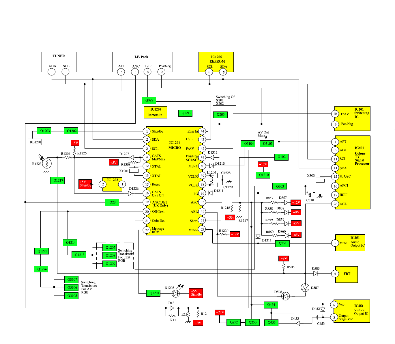
6(&$0 &21 752/ %/2&. ',$*5$0
Page 35
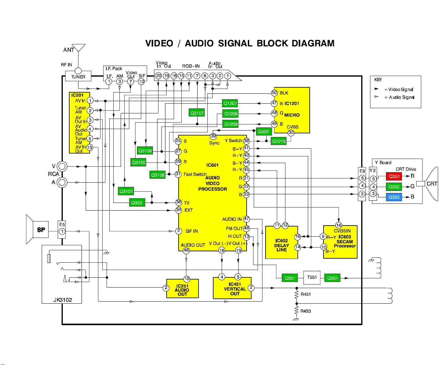
Page 36
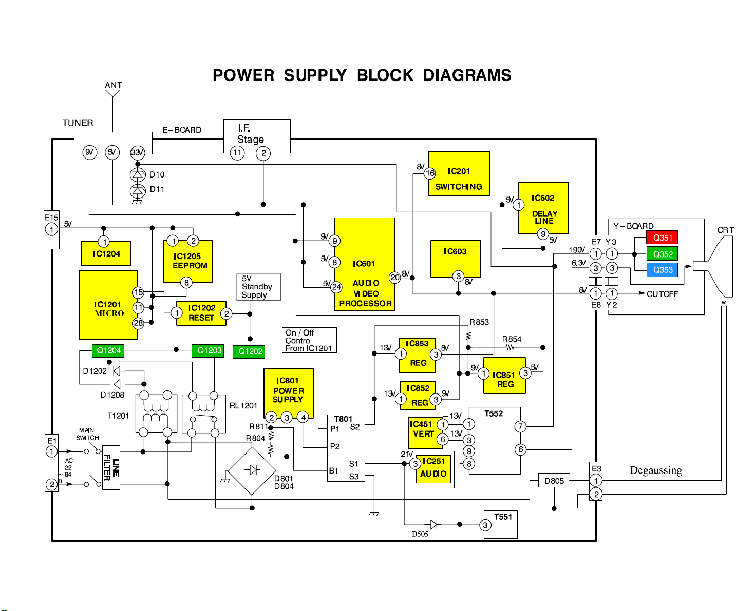
0,&52
Page 37
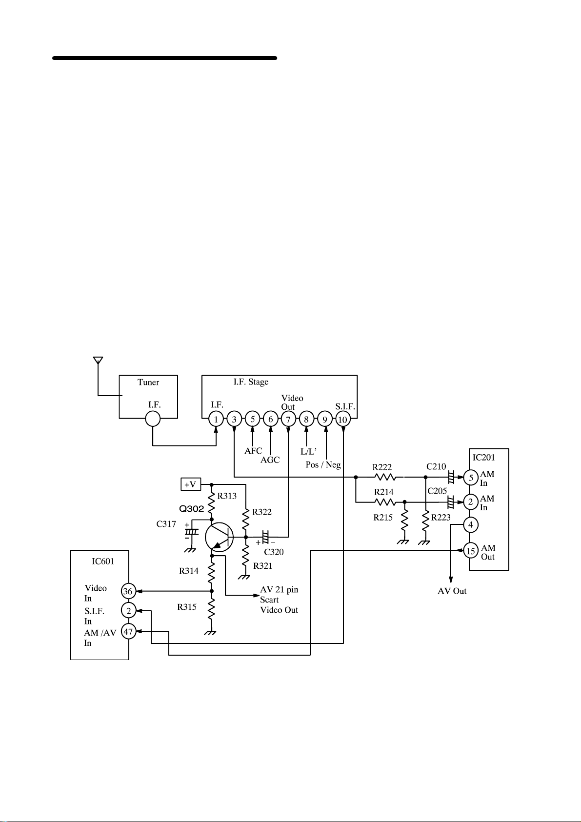
14.4. SECAM I.F. Processing
3DQDVRQLF
Those models which are capable of processing
SECAM L signals have added an additional I.F.pack.
This I.F.pack is responsible for the processing of the
I.F. signal output from the tuner to the relevant video
and audio signals that are required.
The I.F. signal fed from the I.F. pin of the tuner is fed
to pin 1 of the I.F. pack. Here the I.F. signal is
processed and outputs the following signals:
: The video signal output from pin 7 of the I.F.
stageandisfedviatransistorQ302topin36 ofIC601.
Herethevideosignalprocessing described in
is followed.
7.2.
: The S.I.F. signal fed from pin 10 of the I.F.pack
is used to provide FM processing, this SIF signal
being input directly via pin 2 of IC601.
: For AM audio processing, the AM audio signal
is output via pin 3 of the I.F.pack and fed to switching
IC IC201 (described in
The AM audio signal before being input to IC201 is
split in totwo paths. The first path feeds the AM signal
viaresistor R222 / C210 to pin 5 this signal then being
section 14.5.
).
section
switched to the AV21pinscartout.Thesecondfeeds
the split AM audio signal via R214 and C205 to pin 2
of IC201, this audio signal is then output from pin 15
of IC201 and applied to pin 47 of IC601.
Here the audio signal follows the processing path
described in
As well as the outputs from the I.F. stage just
mentioned a number of control lines are input to the
I.F. pack, these being:
: AFC control input pin 5 of theI.F. pack fed from
IC601 pin 1
: AGC control input pin 6 of the I.F. pack and
again fed from IC601 pin 3.
: SECAM L/L’ control line which is output from
the microprocessor IC1201 pin 43 is input via pin 8 of
the I.F. pack.
: Positive / Negative switching as mentioned in
a previous section which is controlled by the
microprocessor pin 44 is input via pin 9 of the I.F.
Pack.
section 7.7.
Page 38
3DQDVRQLF
14.5. Additional Switching Control
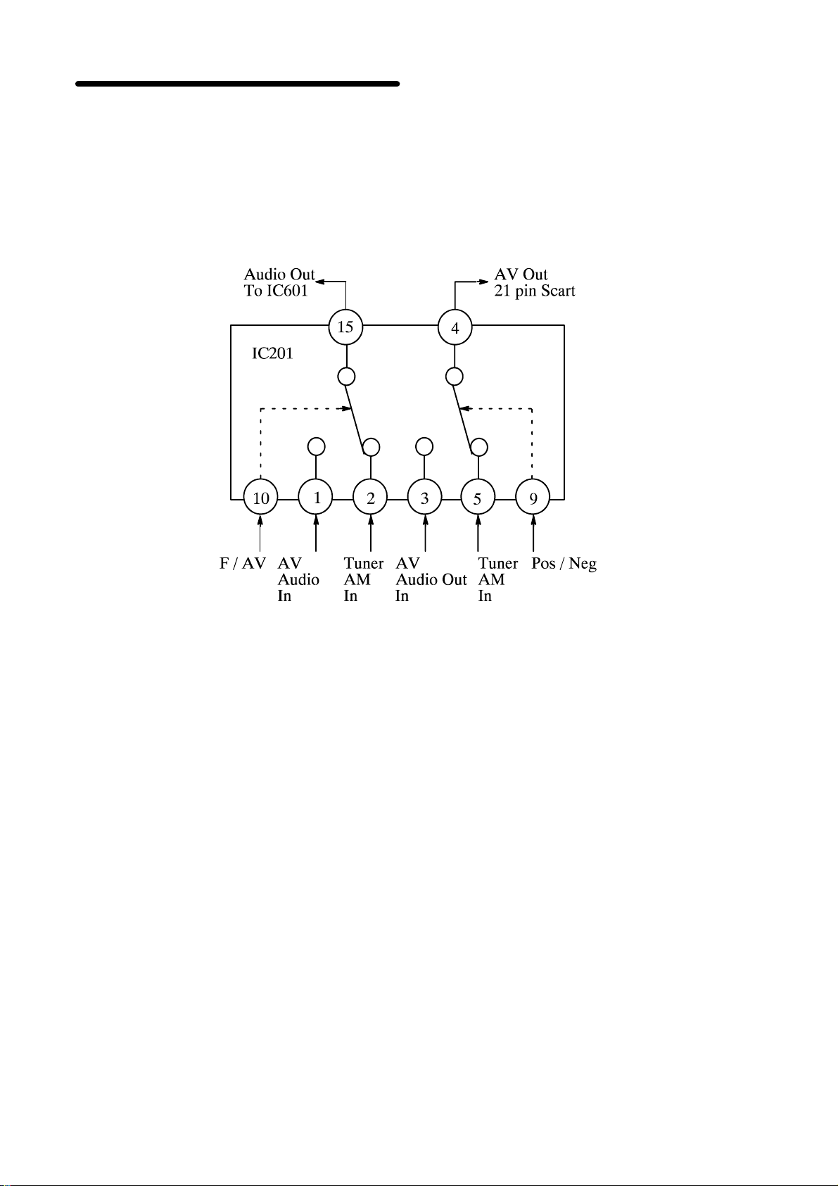
French SECAM models require an additional
switching IC which is provided by IC201 HEF4053.
This additional switching IC is controlled by the
microprocessor IC1201 pin 41 and 42, these control
lines being fed to pins 9 and 10 of IC201 controlling
the internal switching of this IC and the various inputs
listed below:
: Pin 1 - AV audio input, output pin 15
: Pin 2 - Tuner AM input, output pin 15
: Pin 3 - AV audio out input, output pin 4
: Pin 5 - AM audio input, output pin 4
Page 39

3DQDVRQLF
15. ALIGNMENT SETTINGS
1. Select program position 60 and set the sharpness to minimum.
2. Press the Off Timer button on the remote control and at the same time press the V (down) button on the
customer controls at the front of the TV, this will place the TV into Service Mode.
3. Press the
Á / Â buttons to step up / down through the functions.
4. Press the + / - buttons to alter the function values.
5. Press the STORE button after each adjustment has been made to store the required values.
6. To exit Service Mode press the Normalization button.
NOTE : The figures used below are nominal and used for representative purposes only
Alignment Function
1. Vertical amplitude V-Amp
2. Vertical position V-Pos
3. Horizontal centre H-Ctr
4. Red cutoff R-Cut
5. Green cutoff G-Cut
Screen Display
27
03
07
186
Settings / Special Features
Optimum setting
Optimum setting
Optimum setting
Optimum setting
Optimum setting
220
6. Blue cutoff B-Cut
213
7. Red drive R-Drv
46
8. Blue drive B-Drv
36
9. AGC AGC
33
10. Sub contrast S-Con
33
11. Sub colour S-Col
39
12. Sub bright S-Bri
40
Optimum setting
Optimum setting
Optimum setting
Optimum setting
Optimum setting
Optimum setting
Optimum setting
Page 40
3DQDVRQLF
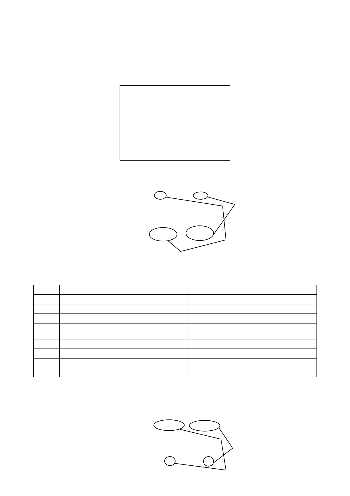
16. SELF CHECK
Self check is used to automatically check the Bus Lines Hexadecimal code of the TV set.
To get into the Self Check mode press the Status button on the Remote Control, followed by the V button on
the customer controls at the front of the TV, and the screen will show:-
237
3OHDVH UHIHU WR DSSURSULDWH
6HUYLFH 0DQXDO IRU +(; YDOXH
How to convert a hexadecimal value to binary
Example Value: 02
+H[ 1R
%LQDU\ 9DOXH
2SWLRQ %LWV
%LQDU\ 'DWD
17. OPTION BYTES
The Hexadecimal number which is displayed in Self Check mode refers to the Option Bytes listed below.
Bit
0 UHF Only UHF / VHF / Hyper
1 Without C.A.T.S. With C.A.T.S.
2 Without System L’ With System L’
3
*
4 Without Fine Tuning With Fine Tuning
5 English Only 7 Languages
6 EC for UK EC other
7 Video Blanking Off Video Blanking On
Option Byte 0 Option Byte 1
TOP Text Disabled
(TV Mode)
TOP Text Enabled
(Monitor Mode)
* Only available for non-text East European models.
How to convert a binary value to a hexadecimal value
Example Value: 00100000
2SWLRQ %LWV
%LQDU\ 'DWD
%LQDU\ 9DOXH
+H[ 1R
 Loading...