

Panasonic XP01554 Datasheet
Composite Transistors
2.1±0.1
0.425
1.25±0.1
0.2±0.05
2.0±0.1
0.65
1
2
3
4
5
0.9± 0.1
0.7±0.1
0.2
0 to 0.1
0.12
+0.05
– 0.02
0.2±0.1
0.425
0.65
XP1554
Silicon NPN epitaxial planer transistor
For high speed switching
Features
■
●
Two elements incorporated into one package.
(Emitter-coupled transistors)
●
Reduction of the mounting area and assembly cost by one half.
●
Low V
Basic Part Number of Element
■
●
2SC3757 × 2 elements
Absolute Maximum Ratings (Ta=25˚C)
■
Parameter Symbol Ratings Unit
Rating
of
element
Overall
.
CE(sat)
Collector to base voltage
Collector to emitter voltage
Emitter to base voltage
V
V
V
Collector current I
Peak collector current
Total power dissipation
Junction temperature
Storage temperature
T
I
P
CBO
CES
EBO
C
CP
T
T
stg
40 V
40 V
5V
100 mA
300 mA
150 mW
j
150 ˚C
–55 to +150 ˚C
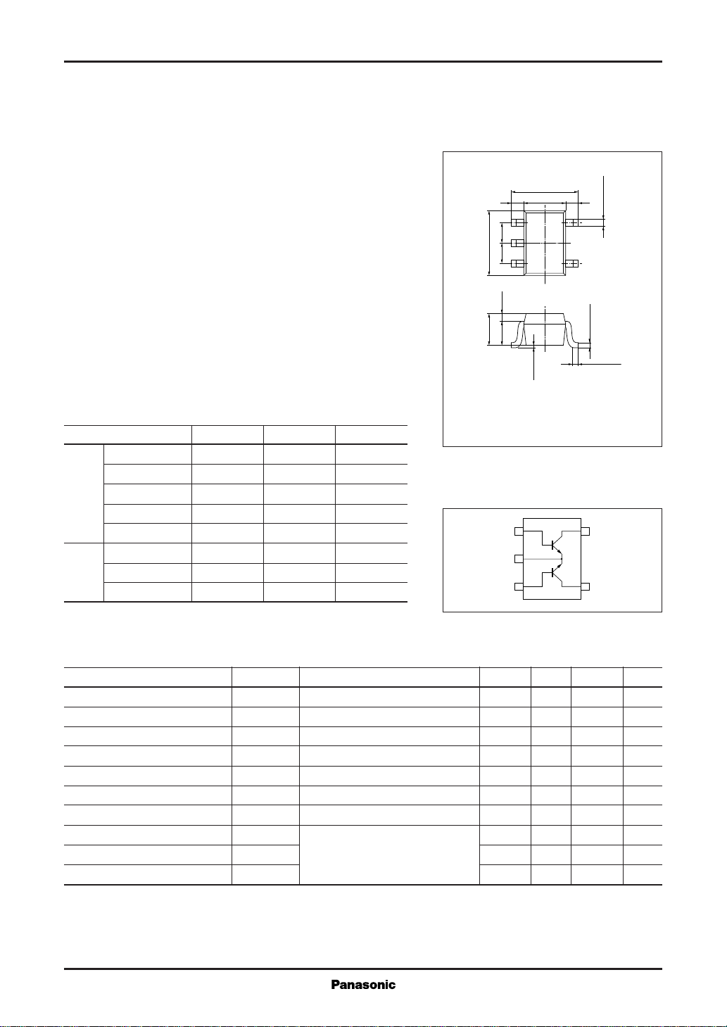
1 : Base (Tr1) 4 : Collector (Tr2)
2 : Emitter 5 : Collector (Tr1)
3 : Base (Tr2) EIAJ : SC–88A
S–Mini Type Package (5–pin)
Marking Symbol: EU
Internal Connection
Tr1
15
2
34
Tr2
Unit: mm
Electrical Characteristics (Ta=25˚C)
■
Parameter Symbol Conditions min typ max Unit
Collector cutoff current I
Emitter cutoff current I
Forward current transfer ratio h
Collector to emitter saturation voltage
Base to emitter saturation voltage V
Transition frequency f
Collector output capacitance C
Turn-on time t
Turn-off time t
Storage time t
CBO
EBO
V
T
on
off
stg
FE
CE(sat)
BE(sat)
ob
VCB = 15V, IE = 0 0.1 µA
VEB = 4V, IC = 0 0.1 µA
VCE = 1V, IC = 10mA 60 200
IC = 10mA, IB = 1mA 0.17 0.25 V
IC = 10mA, IB = 1mA 1.0 V
VCB = 10V, IE = –10mA, f = 200MHz
450 MHz
VCB = 10V, IE = 0, f = 1MHz 2 6 pF
17 ns
17 ns
10 ns
1
Composite Transistors
ton, t
T est Circuit t
off
0.1µF
V
=10V
in
50Ω
V
in
V
out
3.3kΩ
t
10%
on
3.3kΩ
V
bb
–3V
90%
220Ω
=
50Ω
=3V
V
CC
V
in
V
out
t
off
10%
V
90%
XP1554
P
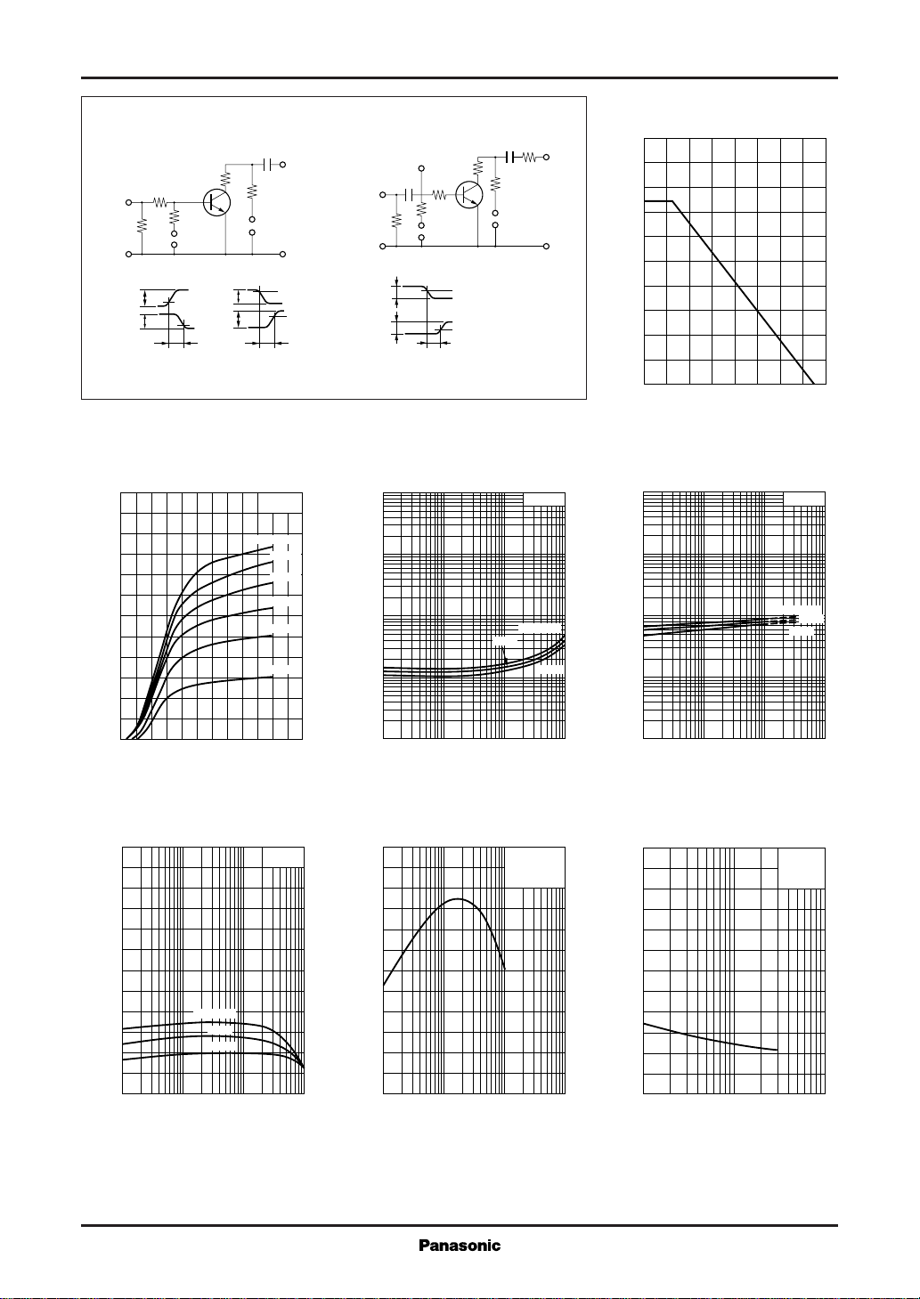
— Ta
Test Circuit
stg
0.1µF
910Ω
10%
10%
out
Vin=10V
0.1µF
50Ω
0
V
in
V
out
(Wave form at A)
A
500Ω
500Ω
V
bb
t
stg
=2V
1kΩ
90Ω
VCC=10V
V
out
200
180
)
160
mW
(
T
140
120
100
80
60
40
Total power dissipation P
20
0
02040 8060 140120100 160
Ambient temperature Ta (˚C
T
)
IC — V
120
100
)
mA
(
80
C
60
40
Collector current I
20
0
01.20.2 1.00.4 0.80.6
Collector to emitter voltage VCE (V
hFE — I
600
FE
500
400
300
CE
C
Ta=25˚C
IB=3.0mA
2.5mA
2.0mA
1.5mA
1.0mA
0.5mA
VCE=1V
V
— I
CE(sat)
100
)
V
(
30
CE(sat)
10
3
1
0.3
0.1
0.03
Collector to emitter saturation voltage V
0.01
0.1 0.3
)
1 3 10 30 100
Collector current IC (mA
fT — I
600
)
500
MHz
(
T
400
300
E
25˚C
C
VCB=10V
Ta=25˚C
IC/IB=10
Ta=75˚C
–25˚C
)
100
)
V
(
30
BE(sat)
10
0.3
0.1
0.03
Base to emitter saturation voltage V
0.01
)
pF
(
ob
V
— I
BE(sat)
3
1
13
10 30 100 300 1000
Collector current IC (mA
Cob — V
6
5
4
3
CB
C
Ta=–25˚C
f=1MHz
I
Ta=25˚C
E
I
C/IB
75˚C
=0
=10
25˚C
)
200
100
Forward current transfer ratio h
0
0.1 0.3
Ta=75˚C
25˚C
–25˚C
1 3 10 30 100
Collector current IC (mA
2
200
100
Transition frequency f
2
1
Collector output capacitance C
0
–1 –3 –10 –30 –100 –300 –1000
)
Emitter current IE (mA
)
0
3 10 30 100
1
Collector to base voltage VCB (V
)
 Loading...