

Panasonic XN06534 Datasheet
Composite Transistors
2.8
+0.2
–0.3
1.50.65±0.15 0.65±0.15
1
6
5
4
3
2
1.45±0.1
0.95 0.95
1.9±0.1
+0.25
–0.05
0.3
+0.1
–0.05
0.5
+0.1
–0.05
2.9
+0.2
–0.05
1.1
+0.2
–0.1
0.8
0.4±0.2
0 to 0.05
0.16
+0.1
–0.06
0.1 to 0.3
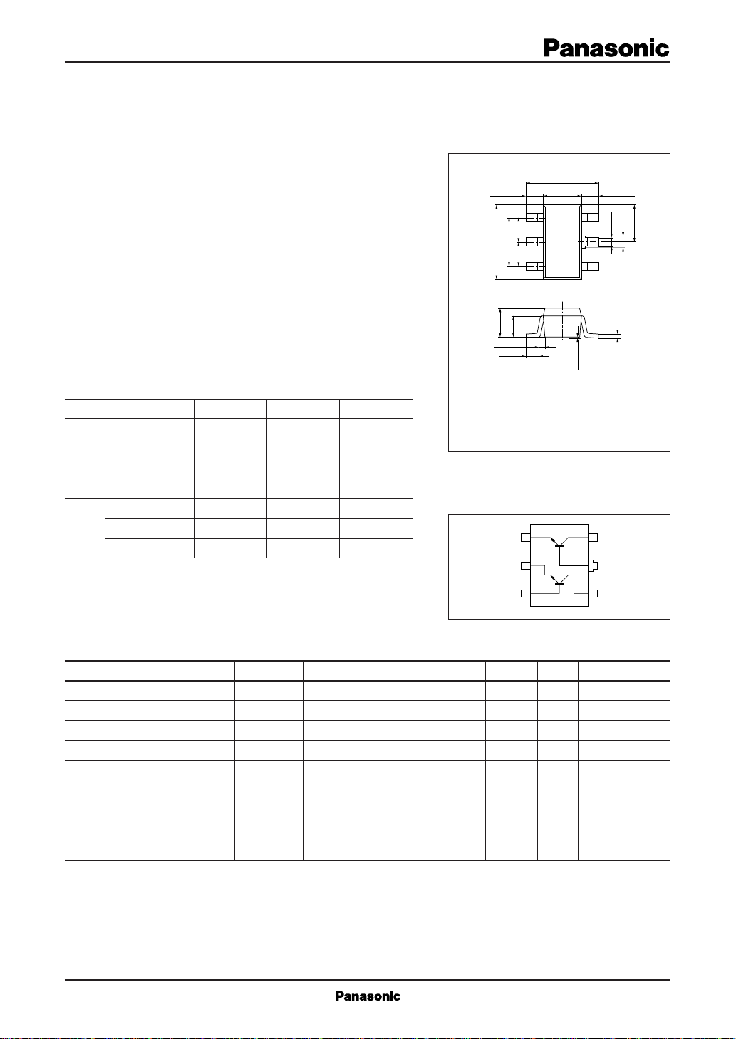
XN6534
Silicon NPN epitaxial planer transistor
For high-frequency amplification
Features
■
●
Two elements incorporated into one package.
●
Reduction of the mounting area and assembly cost by one half.
Basic Part Number of Element
■
●
2SC2404 × 2 elements
Absolute Maximum Ratings (Ta=25˚C)
■
Parameter Symbol Ratings Unit
Collector to base voltage
Rating
Collector to emitter voltage
of
Emitter to base voltage
element
Collector current I
Total power dissipation
Junction temperature
Overall
Storage temperature
V
CBO
V
CEO
V
EBO
C
P
T
T
j
T
stg
30 V
20 V
3V
15 mA
200 mW
150 ˚C
–55 to +150 ˚C
1 : Collector (Tr1) 4 : Base (Tr2)
2 : Base (Tr1) 5 : Emitter (Tr2)
3 : Collector (Tr2) 6 : Emitter (Tr1)
EIAJ : SC–74
Mini Type Package (6–pin)
Marking Symbol: 7F
Internal Connection
Tr1
61
5
Unit: mm
2
43
Tr2
Electrical Characteristics (Ta=25˚C)
■
Parameter Symbol Conditions min typ max Unit
Collector to base voltage V
Emitter to base voltage V
Forward current transfer ratio h
Forward current transfer hFE ratio
Base to emitter voltage V
Common emitter reverse transfer capacitance
Transition frequency f
Noise figure NF VCB = 6V, IE = –1mA, f = 100MHz 3.3 dB
Power gain PG VCB = 6V, IE = –1mA, f = 100MHz 24 dB
*1
Ratio between 2 elements
CBO
EBO
FE
hFE (small/large)*1VCB = 6V, IE = –1mA 0.5 0.99
BE
C
re
T
IC = 10µA, IE = 0 30 V
IE = 10µA, IC = 0 3 V
VCB = 6V, IE = –1mA 40 260
VCB = 6V, IE = –1mA 720 mV
VCB = 6V, IE = –1mA, f = 10.7MHz 0.8 1 pF
VCB = 6V, IE = –1mA, f = 200MHz 450 650 MHz
1
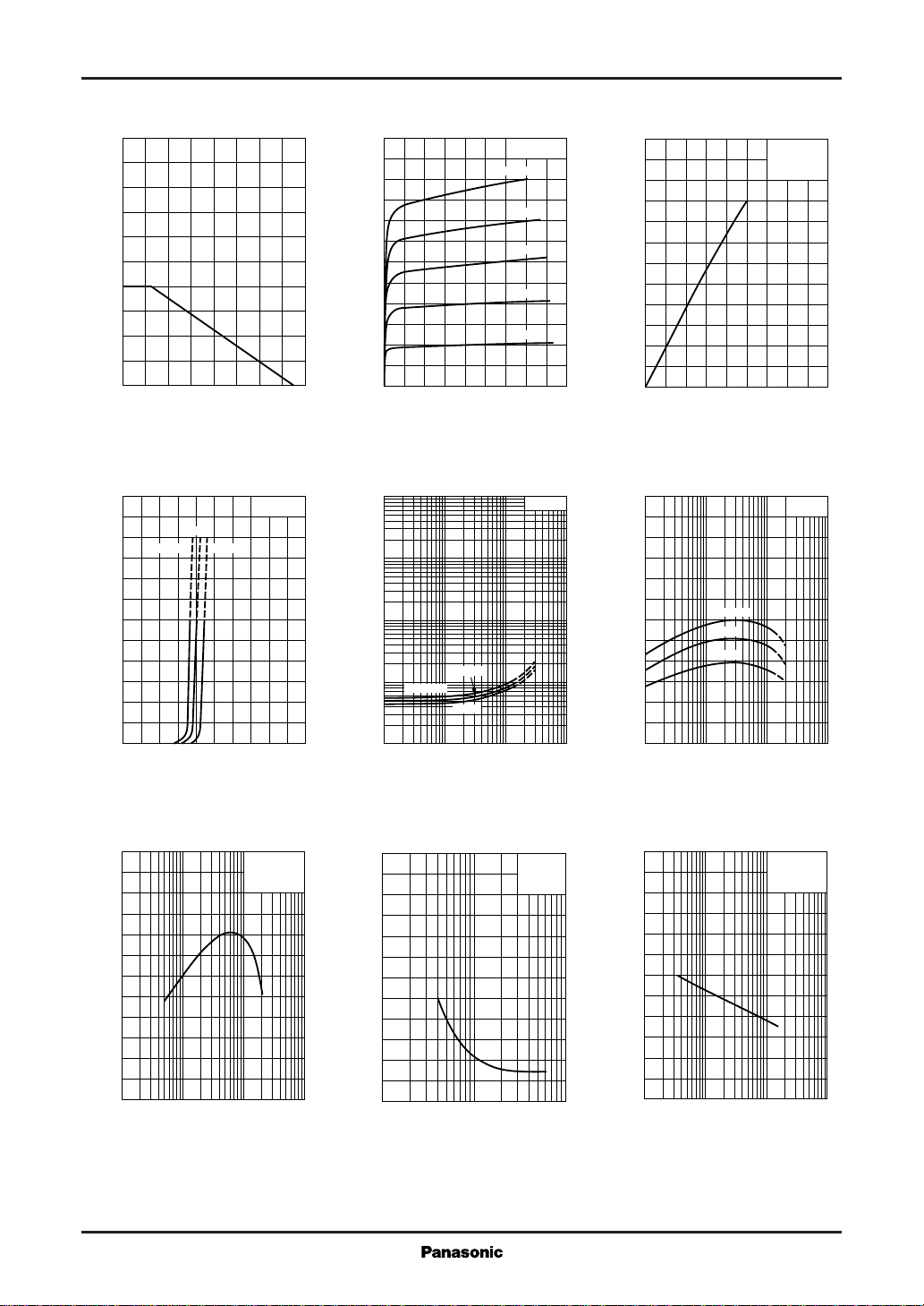
Composite Transistors
XN6534
PT — Ta IC — V
500
)
400
mW
(
T
300
200
100
Total power dissipation P
0
0 40 80 120 160
Ambient temperature Ta (˚C
IC — V
BE
30
25
)
mA
(
20
C
15
10
Collector current I
5
0
02.01.61.20.80.4
Base to emitter voltage VBE (V
25˚C
Ta=75˚C –25˚C
VCE=6V
CE
12
10
)
mA
(
8
C
6
4
Collector current I
2
0
0481216
)
)
Collector to emitter voltage VCE (V
V
CE(sat)
100
)
V
(
30
CE(sat)
10
3
1
0.3
0.1
Ta=75˚C
0.03
Collector to emitter saturation voltage V
0.01
0.1 0.3
–25˚C
1 3 10 30 100
Collector current IC (mA
25˚C
— I
Ta=25˚C
IB=100µA
80µA
60µA
40µA
20µA
)
C
IC/IB=10
)
12
10
)
mA
(
8
C
6
4
Collector current I
2
0
0 40 80 120 160
360
FE
300
240
180
120
60
Forward current transfer ratio h
0
0.1 0.3
IC — I
B
VCE=6V
Ta=25˚C
Base current IB (µA
hFE — I
C
VCE=6V
Ta=75˚C
25˚C
–25˚C
1 3 10 30 100
Collector current IC (mA
)
)
fT — I
E
1200
)
1000
MHz
(
T
800
600
400
200
Transition frequency f
0
–0.1 –0.3 –1 –3 –10 –30 –100
Emitter current IE (mA
2
VCB=6V
Ta=25˚C
Zrb — I
E
)
120
)
Ω
(
100
rb
80
60
40
20
VCB=6V
f=2MHz
Ta=25˚C
pF
(
2.4
re
2.0
1.6
1.2
0.8
0.4
Cre — V
CE
IC=1mA
f=10.7MHz
Ta=25˚C
Reverse transfer impedance Z
Common emitter reverse transfer capacitance C
0
–0.3 –1 –3 –10
)
–0.1
Emitter current IE (mA
)
0
0.1 0.3 1 3 10 30 100
Collector to emitter voltage VCE (V
)
 Loading...