

Panasonic XN01871 Datasheet
Composite Transistors
XN1871
Silicon N-channel junction FET
For amplification of the low frequency
Features
■
●
Two elements incorporated into one package.
(Soure-coupled FETs)
●
Reduction of the mounting area and assembly cost by one half.
Basic Part Number of Element
■
●
2SK198 × 2 elements
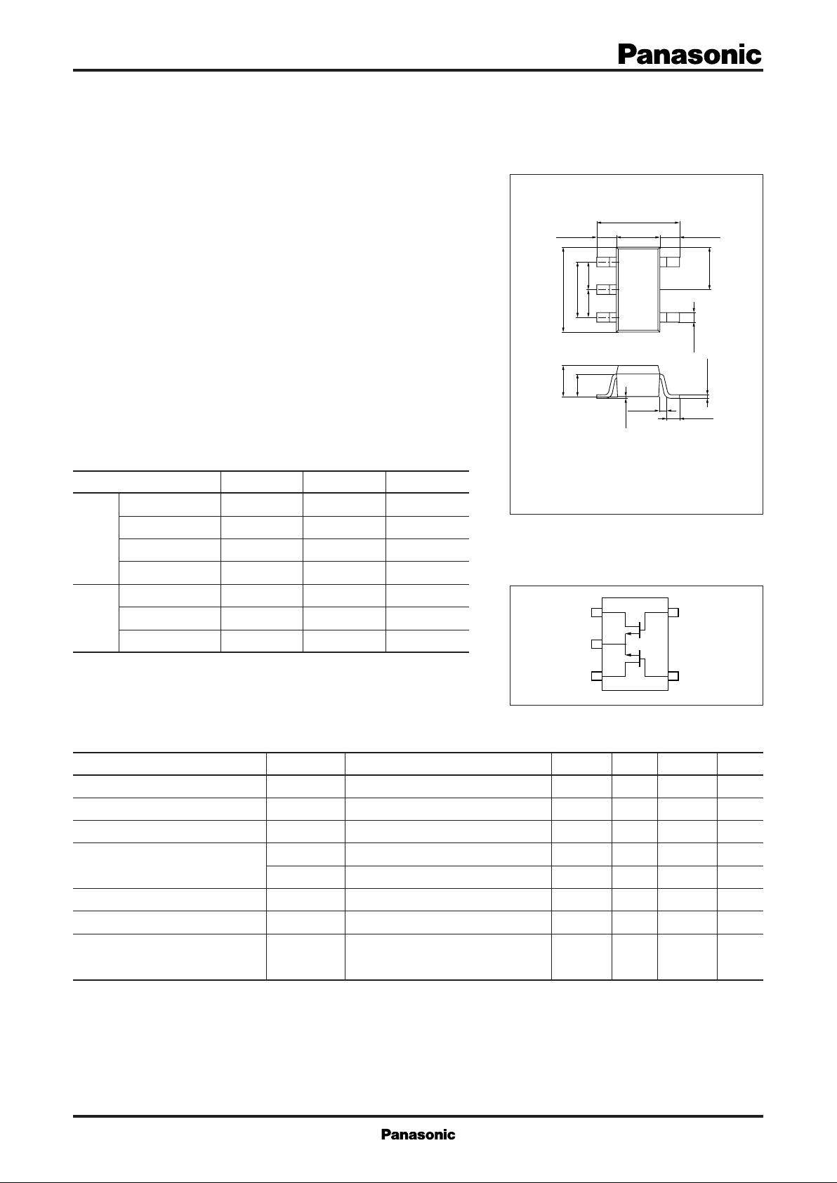
Absolute Maximum Ratings (Ta=25˚C) 1 : Gate (Tr1) 4 : Source
■
Rating
of
element
Overall
Parameter Symbol Ratings Unit
Drain to source voltage
Gate to drain voltage
Drain current I
Gate current I
Total power dissipation
Channel temperature
Storage temperature
V
DSX
V
GDO
D
G
P
T
T
ch
T
stg
30 V
–30 V
20 mA
10 mA
300 mW
150 ˚C
–55 to +150 ˚C
2 : Gate (Tr2) 5 : Drain (Tr1)
3 : Drain (Tr2) EIAJ : SC–74A
Marking Symbol: 5T
Internal Connection
4
0.05
+0.2
-
2.9
1.9±0.10.8
3
0.95 0.95
0.1
+0.2
-
1.1
5
4
Unit: mm
+0.2
-
0.3
2.8
+0.25
-
0.05
1.50.65±0.15 0.65±0.15
15
1.45±0.1
2
0.05
+0.1
-
0.3
0.06
+0.1
-
0.16
0.1 to 0.3
0 to 0.1
0.4±0.2
Mini Type Pakage (5–pin)
FET 1
1
Electrical Characteristics (Ta=25˚C)
■
Parameter Symbol Conditions min typ max Unit
Drain current I
Gate cutoff current I
Gate to source cutoff voltage V
DSS
GSS
GSC
gm VDS = 10V, ID = 0.5mA, f = 1MHz 4 mS
Mutual conductance
gm VDS = 10V, VGS = 0V, f = 1MHz 4 12 mS
Common source short-circuit input capacitance
Common source reverse transfer capacitance
C
iss
C
rss
Noise voltage NV
32
FET 2
VDS = 10V, VGS = 0 0.5 12 mA
VGS = –30V, VDS = 0 –100 nA
VDS = 10V, ID = 10µA – 0.1 –1.5 V
VDS = 10V, VGS = 0V, f = 1MHz 14 pF
VDS = 10V, VGS = 0V, f = 1MHz 3.5 pF
VDS = 30V, ID = 1mA, GV = 80dB
Rg = 100kΩ, Function = FLAT
60 mV
1

Composite Transistors XN1871
PT — Ta ID — V
500
)
400
mW
(
T
300
200
100
Total power dissipation P
0
0 40 80 120 160
Ambient temperature Ta (˚C
gm — V
20
18
)
16
mS
(
14
m
12
10
8
6
4
Mutual conductance g
2
0
–0.8 –0.6 –0.4 –0.2 0
Gate to source voltage VGS (V
I
DSS
GS
=5.0mA
2.0mA
VDS=10V
Ta=25˚C
DS
8
7
)
6
mA
(
5
D
4
3
Drain current I
2
1
0
012210486
)
Drain to source voltage VDS (V
gm — I
20
18
)
16
mS
(
14
m
12
10
8
6
4
Mutual conductance g
2
0
02468
)
=5.0mA
I
DSS
2.0mA
Drain current ID (mA
Ta=25˚C
VGS=0V
–0.1V
–0.2V
–0.3V
–0.4V
)
D
VDS=10V
Ta=25˚C
)
9.6
8.0
)
mA
(
6.4
D
4.8
3.2
Drain current I
1.6
0
–1.0 0–0.2–0.4–0.6–0.8
)
10
pF
(
oss
, C
iss
8
C
6
4
2
Common source short-circuit input capacitance,
Common source short-circuit output capacitance
0
1
ID — V
GS
VDS=10V
Ta=75˚C
25˚C
–25˚C
Gate to source voltage VGS (V
C
, C
— V
iss
oss
3 10 30 100550220
DS
VGS=–3V
f=1MHz
Ta=25˚C
C
iss
C
oss
Drain to source voltage VDS (V
)
)
C
— V
)
pF
(
5
rss
4
3
2
1
0
1
Common source reverse transfer capacitance C
rss
3 10 30 100550220
Drain to source voltage VDS (V
DS
VGS=3V
f=1MHz
Ta=25˚C
)
2
NF — f
12
10
)
dB
(
8
6
4
Noise figure NF
2
0
10 100 1k 10k
Frequency f (Hz
Rg=500Ω
1kΩ
VDS=10V
=5.2mA
I
D
Ta=25˚C
)
100k
 Loading...