

Panasonic XN01401 Datasheet
Composite Transistors
XN1401
Silicon PNP epitaxial planer transistor
For general amplification
Features
■
●
Two elements incorporated into one package.
(Emitter-coupled transistors)
●
Reduction of the mounting area and assembly cost by one half.
Basic Part Number of Element
■
●
2SB709A × 2 elements
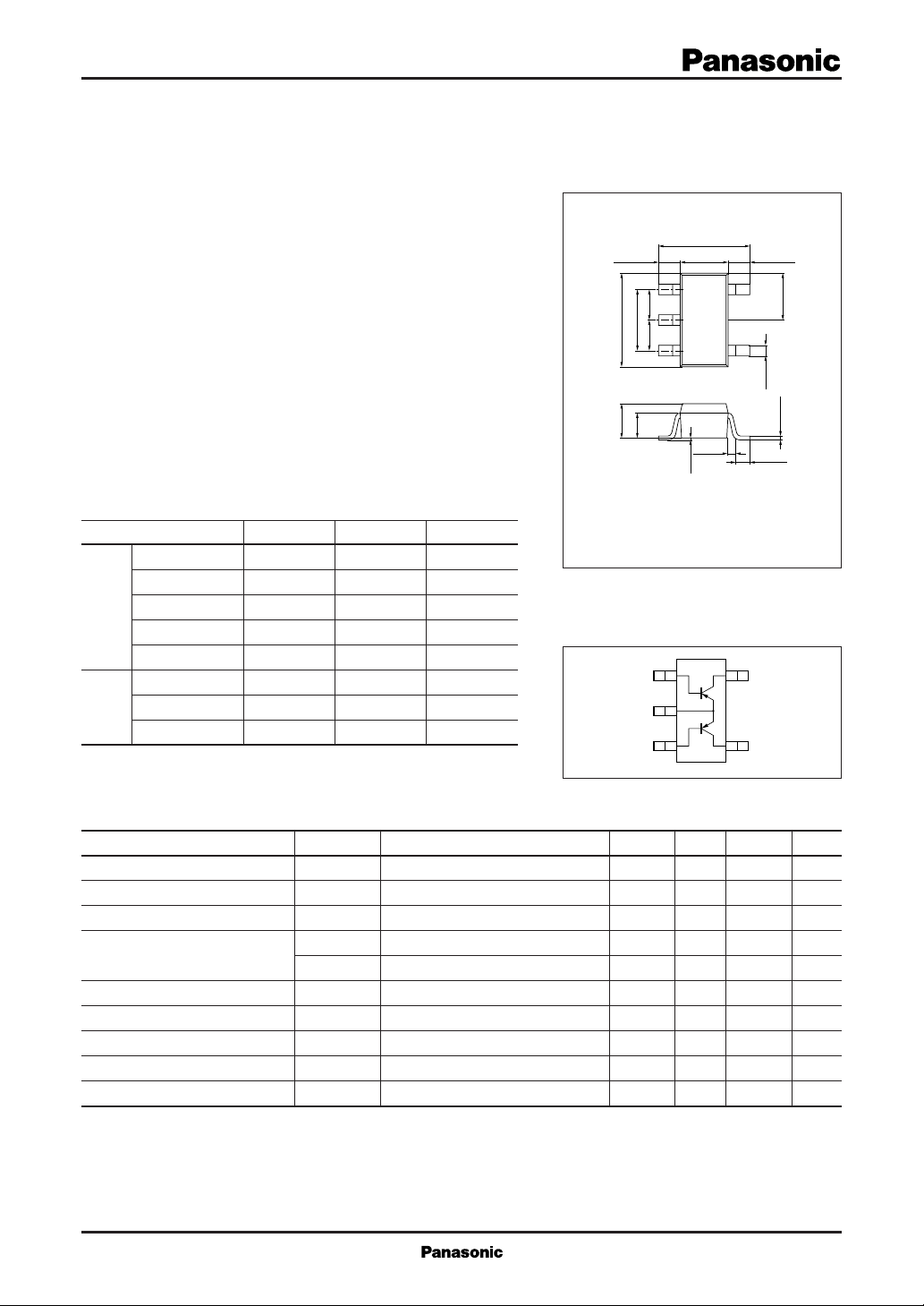
Absolute Maximum Ratings (Ta=25˚C) 1 : Collector (Tr1) 4 : Emitter
■
Parameter Symbol Ratings Unit
Collector to base voltage
Collector to emitter voltage
Rating
Emitter to base voltage
of
element
Collector current I
Peak collector current
Total power dissipation
Junction temperature
Overall
Storage temperature
V
CBO
V
CEO
V
EBO
C
I
CP
P
T
T
j
T
stg
–60 V
–50 V
–7 V
–100 mA
–200 mA
300 mW
150 ˚C
–55 to +150 ˚C
2 : Collector (Tr2) 5 : Base (Tr1)
3 : Base (Tr2) EIAJ : SC–74A
Marking Symbol: 5V
Internal Connection
4
0.05
+0.2
-
2.9
1.9±0.10.8
3
0.95 0.95
0.1
+0.2
-
1.1
5
4
3
Unit: mm
+0.2
-
0.3
2.8
+0.25
-
0.05
1.50.65±0.15 0.65±0.15
15
1.45±0.1
2
0.05
+0.1
-
0.3
0.06
+0.1
-
0.16
0.1 to 0.3
0 to 0.1
0.4±0.2
Mini Type Pakage (5–pin)
Tr1
Tr2
1
2
Electrical Characteristics (Ta=25˚C)
■
Parameter Symbol Conditions min typ max Unit
Collector to base voltage V
Collector to emitter voltage V
Emitter to base voltage V
Collector cutoff current
Forward current transfer ratio h
Forward current transfer hFE ratio
Collector to emitter saturation voltage
Transition frequency f
Collector output capacitance C
*1
Ratio between 2 elements
CBO
CEO
EBO
I
CBO
I
CEO
FE
hFE (small/large)*1VCE = –10V, IC = –2mA 0.5 0.99
V
CE(sat)
T
ob
IC = –10µA, IE = 0 –60 V
IC = –2mA, IB = 0 –50 V
IE = –10µA, IC = 0 –7 V
VCB = –20V, IE = 0 – 0.1 µA
VCE = –10V, IB = 0 –100 µA
VCE = –10V, IC = –2mA 160 460
IC = –100mA, IB = –10mA – 0.3 – 0.5 V
VCB = –10V, IE = 1mA, f = 200MHz 80 MHz
VCB = –10V, IE = 0, f = 1MHz 2.7 pF
1
Composite Transistors XN1401
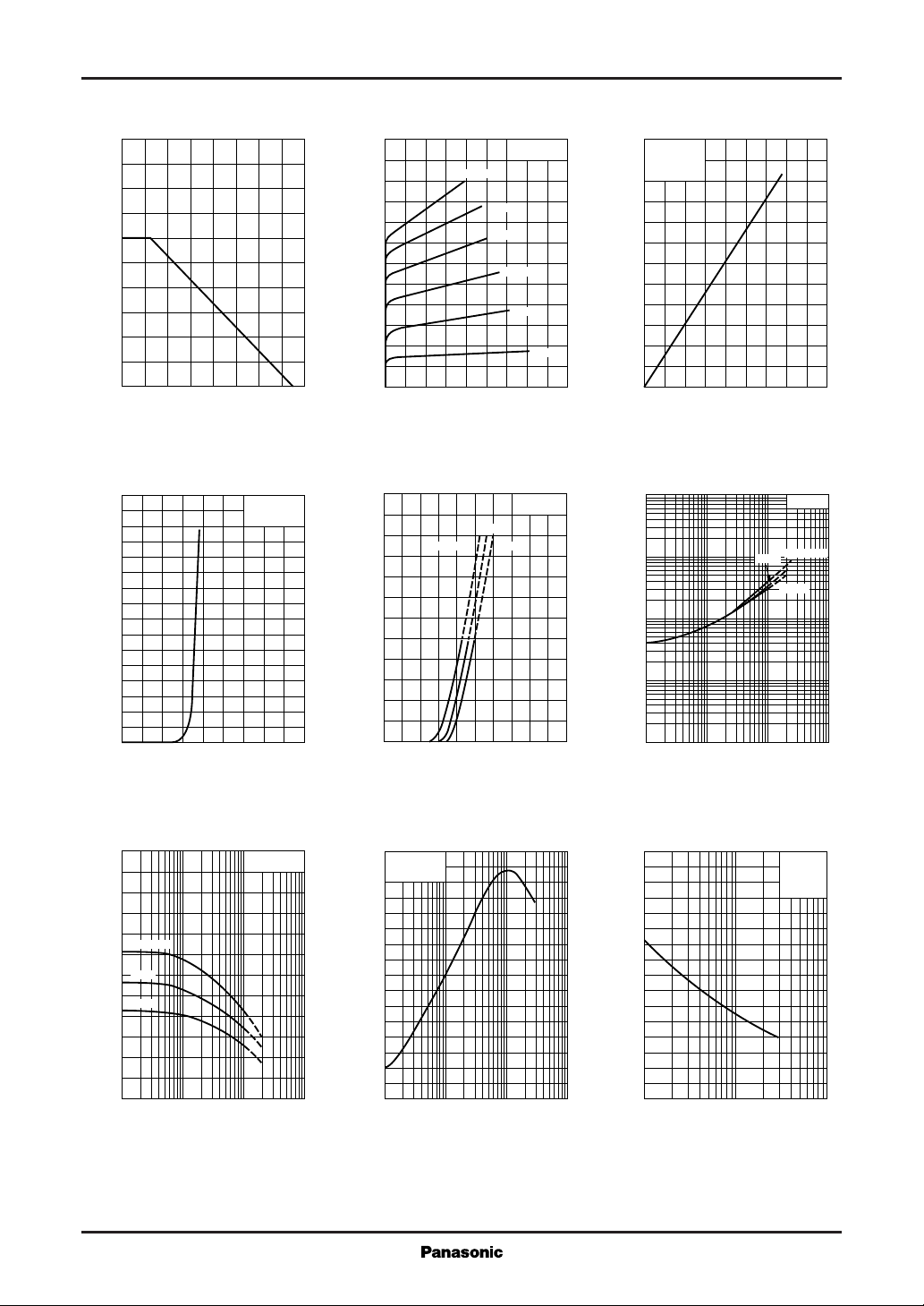
PT — Ta IC — V
500
)
400
mW
(
T
300
200
100
Total power dissipation P
0
0 40 80 120 160
Ambient temperature Ta (˚C
IB — V
BE
–400
–350
)
–300
µA
(
–250
B
–200
VCE=–5V
Ta=25˚C
CE
–60
–50
)
mA
(
–40
C
–30
–20
Collector current I
–10
0
)
0 –18–2 –4 –6 –8 –10 –12–14 –16
Collector to emitter voltage VCE (V
IB=–300µA
IC — V
–240
–200
)
mA
(
–160
C
–120
Ta=75˚C –25˚C
Ta=25˚C
–250µA
–200µA
–150µA
–100µA
–50µA
)
BE
VCE=–5V
25˚C
–60
–50
)
mA
(
–40
C
–30
–20
Collector current I
–10
0
0 –100 –200 –300 –400
–10
)
V
(
–3
CE(sat)
–1
–0.3
–0.1
IC — I
VCE=–5V
Ta=25˚C
Base current IB (µA
V
— I
CE(sat)
B
)
C
IC/IB=10
Ta=75˚C
25˚C
–25˚C
–150
Base current I
–100
–50
0
0 –0.4 –0.8 –1.2 –1.6
Base to emitter voltage VBE (V
hFE — I
C
600
FE
500
400
Ta=75˚C
25˚C
300
–25˚C
200
100
Forward current transfer ratio h
0
–1 –3
–10 –30 –100 –300 –1000
VCE=–10V
Collector current IC (mA
–80
Collector current I
–40
0
0–2.0–1.6–1.2–0.8–0.4
)
)
Base to emitter voltage VBE (V
fT — I
160
VCB=–10V
Ta=25˚C
140
)
MHz
120
(
T
100
80
60
40
Transition frequency f
20
0
0.1 0.3
1 3 10 30 100
Emitter current IE (mA
E
)
)
–0.03
–0.01
–0.003
Collector to emitter saturation voltage V
–0.001
–1 –3
8
)
pF
7
(
ob
6
5
4
3
2
1
Collector output capacitance C
0
–1 –5
–10 –30 –100 –300 –1000
Collector current IC (mA
–2
Cob — V
–3
–10
CB
–20
f=1MHz
I
E
Ta=25˚C
–30
=0
–50
Collector to base voltage VCB (V
)
–100
)
2
 Loading...