Page 1
E-Seminar
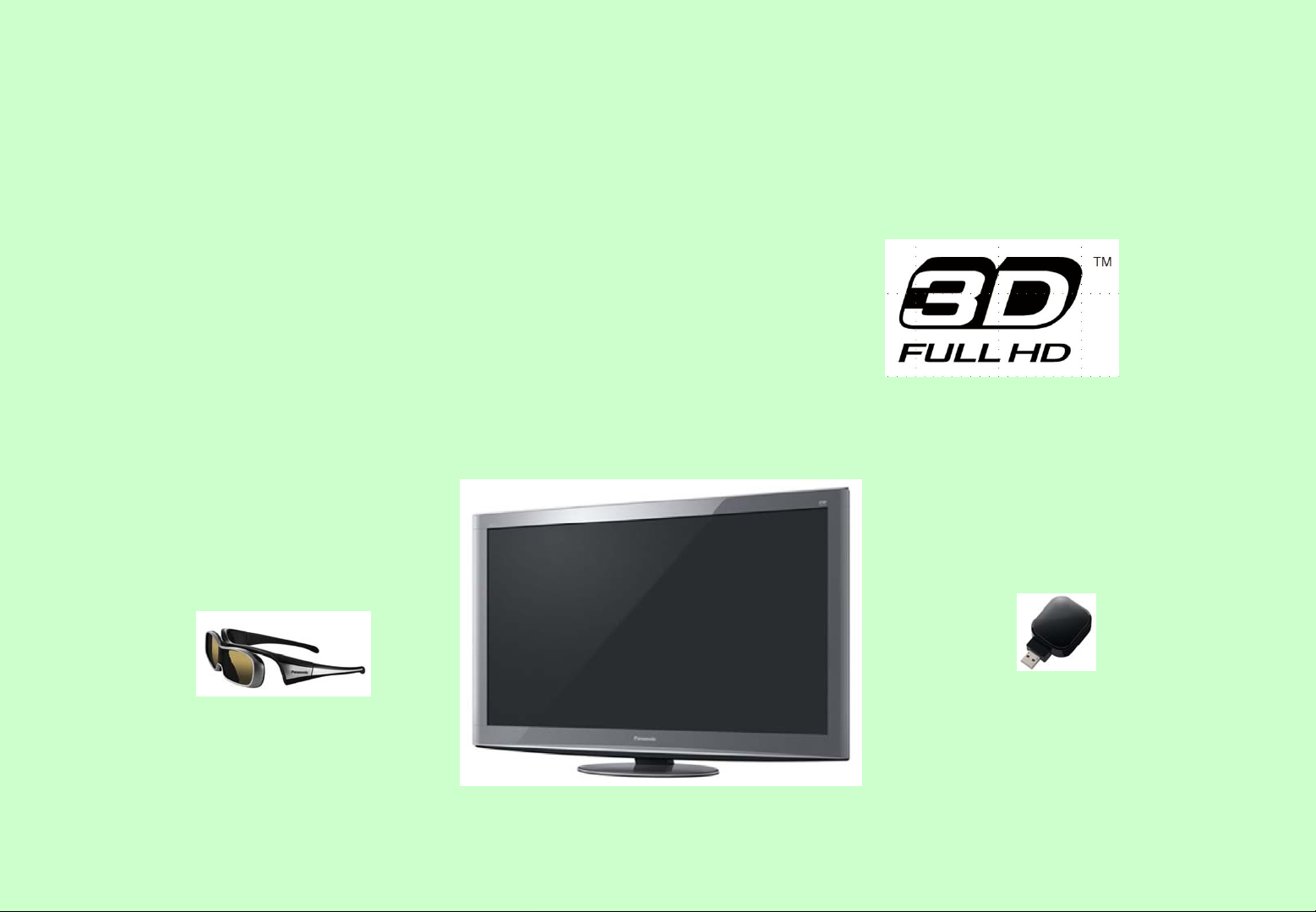
2010 VIErA (FHD 3D PDP)
VT20T series
3D Eyewear
Dongle (Wi-Fi)
1
Page 2

Table of Contents
Lesson 1 Explanation about 3D
Lesson 2 Chassis structure and Signal circuit
Lesson 3 Picture Problem
Lesson 4 Power Supply Circuit
Lesson 5 Protection Circuit
Lesson 6 Troubleshooting of Power Supply Circuit
Lesson 7 Service Information
2
Page 3

1. Explanation about 3D
3
Page 4
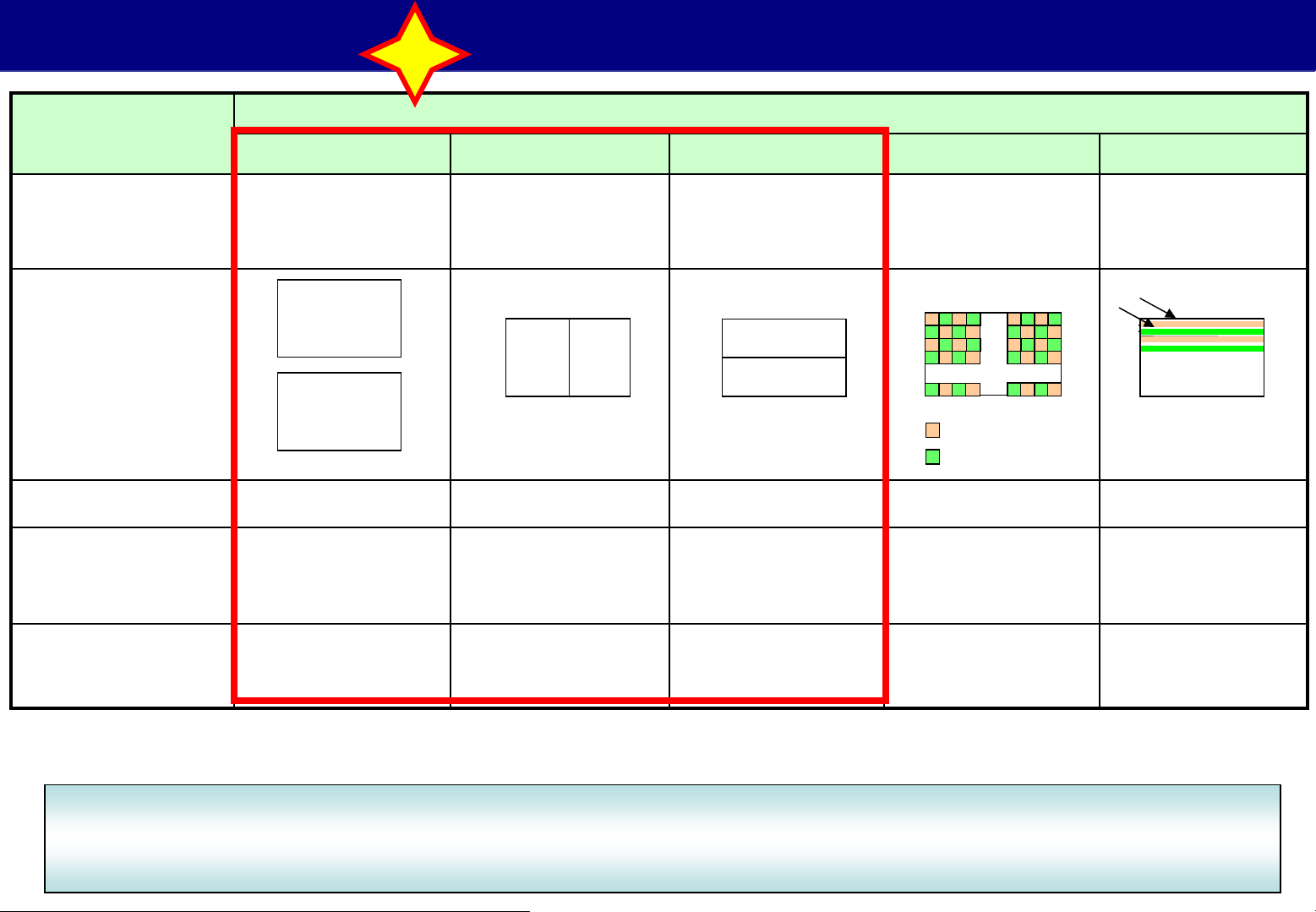
1-1. 3D Format
Item
Frame Sequential Side by Side (SBS)
New
(FS)
3D Signal Method
Top & Bottom (T&B)
4/12
Checker Pattern Line by Line
Input HDMI Ver. 1.4
L
Image
R
Support Situation
Setting method HDMI Ver1.4:Auto
Remarks
BD contents use
this FS format.
○○ ××
HDMI Ver/1.4/
HDMI Ver.1.3 under/
broadcasting
L R
HDMI Ver1.4:Auto
Other: User manual
setting
Under HDMI
Ver.1.3/
broadcasting
L
R
○
User manual
setting
BD-recorder cannot
accept this T&B
format.
Digital signal from
PC etc.
…
…
L
R
Format used for PC
etc.
HDMI Ver.1.4
L
R
- Only HDMI Ver. 1.4 is possible for the automatic recognition of 3D signal.
- 3D signal is only for the digital input. (PC and an external analog input, etc. do not accept 3D signal.)
3D format has not been fixed yet.
If the customer use other brand DVD, please confirm the format and/or TV setting.
For details, please confirm Operation Manual.
4
Page 5
1-2. Full HD 3D Technology (1/2)
2/12
New
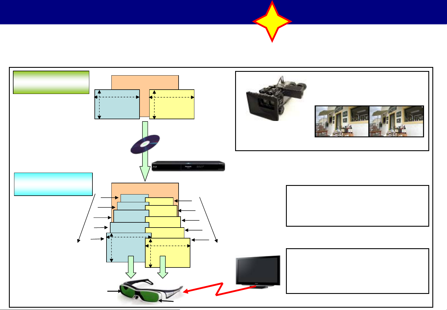
Panasonic selected the frame sequential method.
This brings cinema-level images right into the living room, without the problems of image deterioration and blurring
that were common to conventional 3D systems.
Original Master 3D
images for theaters
Played with the Frame
Sequential Method
60 Frames
(50 Frames : PAL)
For the right eye
1920
1080
For the left eye For the right eye
R
R
R
R
R
1920
1080
1920
1080
3D Blu-ray Disc
3D Blu-ray Disc Player
L
1920
1080
(Infrared Rays)
L
L
60 Frames
(50 Frames : PAL)
L
L
IR
3D special camera
R (right) and L (left) images are
alternately displayed at high speed
(60 (50:PAL) frames/secon d x 2 =120
(100: PAL) frames).
A special camera records images
for the left and right eyes.
Full HD x 2
left
When viewed with special LCD
shutter glasses (3D Eyewear),
the brain creates the sensation of
depth from the visual disparity to
form 3D images.
Right
3D eyewear
For the left eye
5
Page 6
1-2. Full HD 3D Technology (2/2)
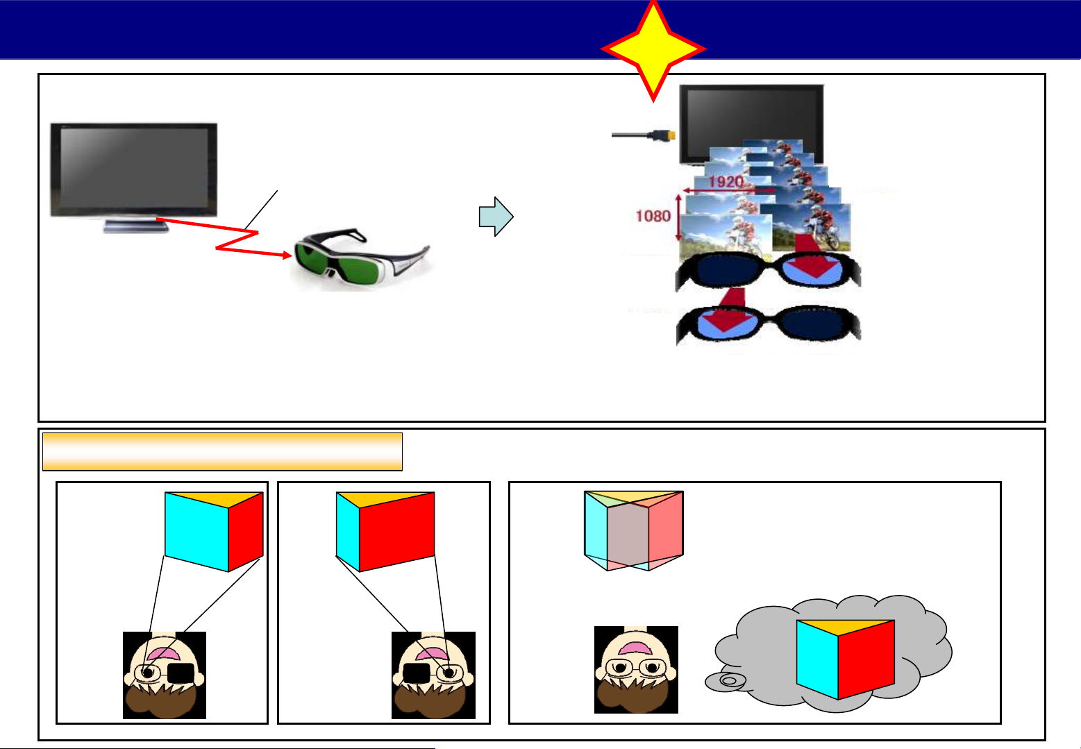
Open/close timing of the liquid crystal
shutter is controlled by receiving IR
signals from the TV, which provide
3D expression of the images.
New
Single eye 60 (50)
frames/sec x 2 :
= 120 (100) frames/sec
IR (Infrared Rays )
Vision principle with 3D glasses
Image for
left eye
Image for
right eye
When you see
a right image
When you see
a left image
A right and left image is switched
with glasses at high speed.
Recognized the stereoscopic vision
according to parallaxes of right and
left eyes.
Composite
image
6
Page 7
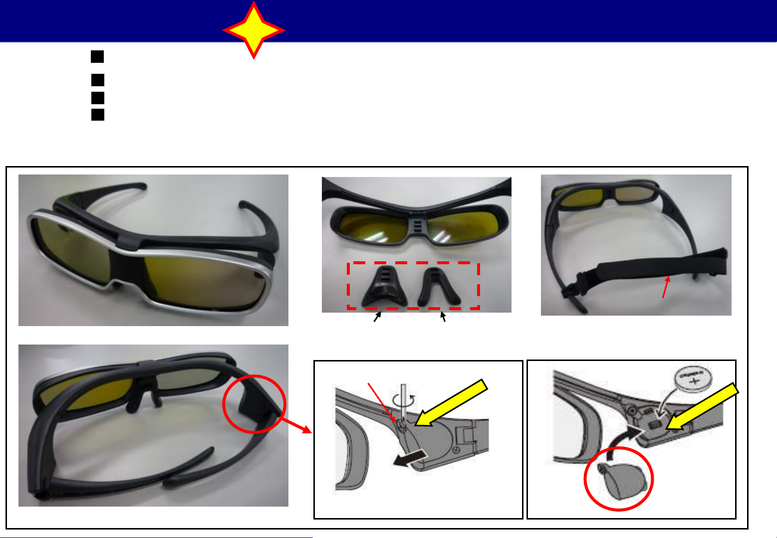
1-3. 3D Eyewear
New
5/12
Product Name
SYNC system
IR receiving distance
: 3D Glass
: 120Hz Frame Sequential System
: about 3.2m
Power : Battery (CR2032) ※Battery Life : About 100Hrs
Nose Pad - A
Nose Pad - B
Kids Band
Screw
Battery Holder
n
io
t
n
e
t
t
a
a
n
io
t
n
e
t
t
Battery
Cover
7
Page 8

2. Chassis Structure and Signal Circuit
8
Page 9
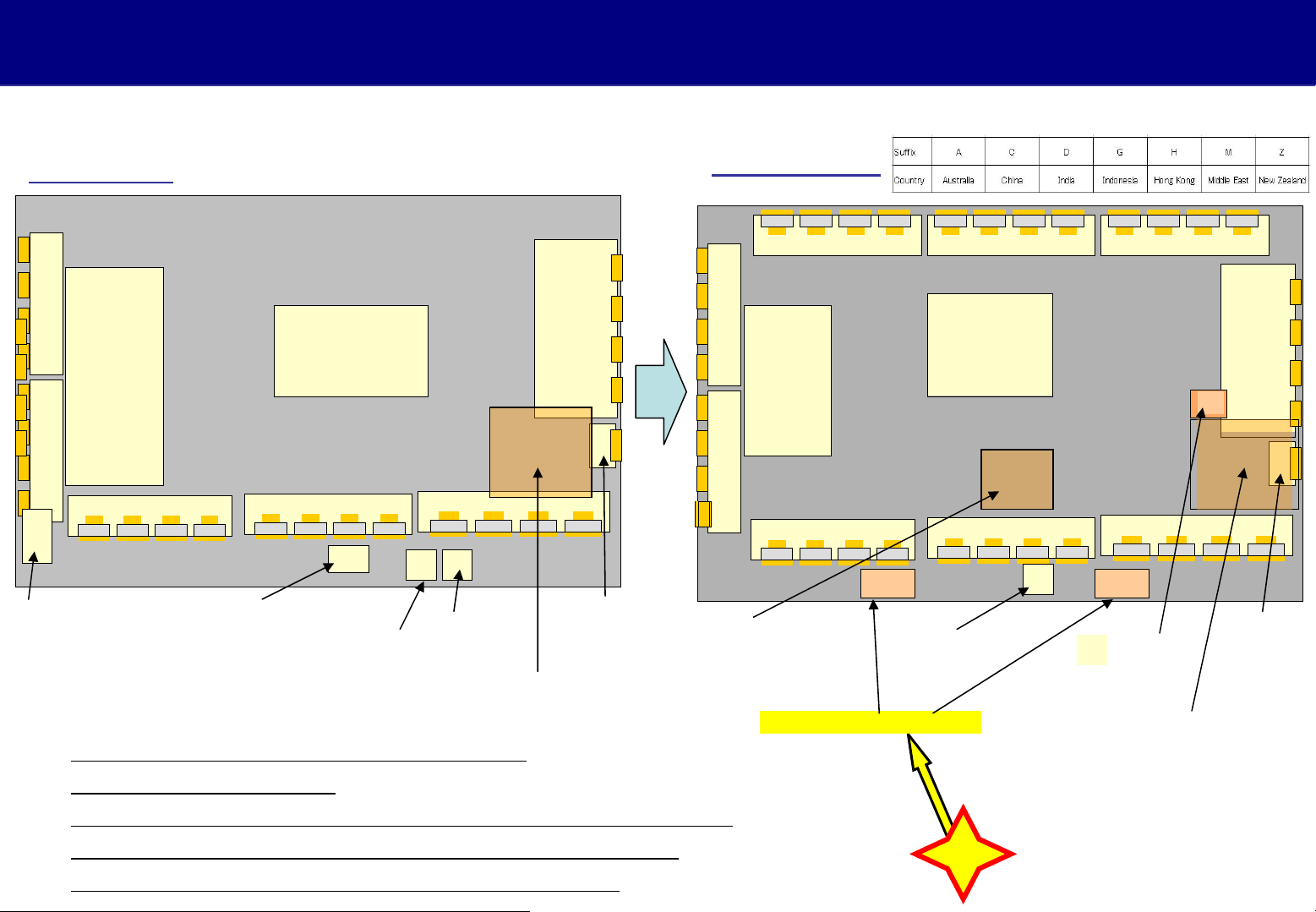
2-1. Chassis Structure (With
different points form current model)
different points form current model)
P50V10
SU
SC
Scan Drive
SD
C1
GK
Key Switch
Remote receiver, Power LED, C.A.T.S sensor
SD blue LED
Different points from current model
Power
Supply
C2
Digital Signal Processor, Format Converter,
Plasma AI, Su-field Processor
P
GL
K
S
Power
Switch
A
C3
SS
Sustain
Drive
SS2
Sustain out
P50VT20
SU
SC
Scan Drive
SD
C1
Format Converter,
Plasma AI,
Sub-Field Processor
Transmitter for 3D eyewear
C5C4 C6
P
Power
Supply
D
C2
V
Remote receiver,
Power LED
K
V
Additional
Digital
Tuner
Digital Signal
Processor
SS
Sustain
Drive
XH
A
C3
SS2
Sustain out
1. D board is added.
2. Power switch is moved from S board to A board.
3. V board is transmitter board for 3D eyewear.
4. XH board is used in China, Hong Kong.
New
9
Page 10
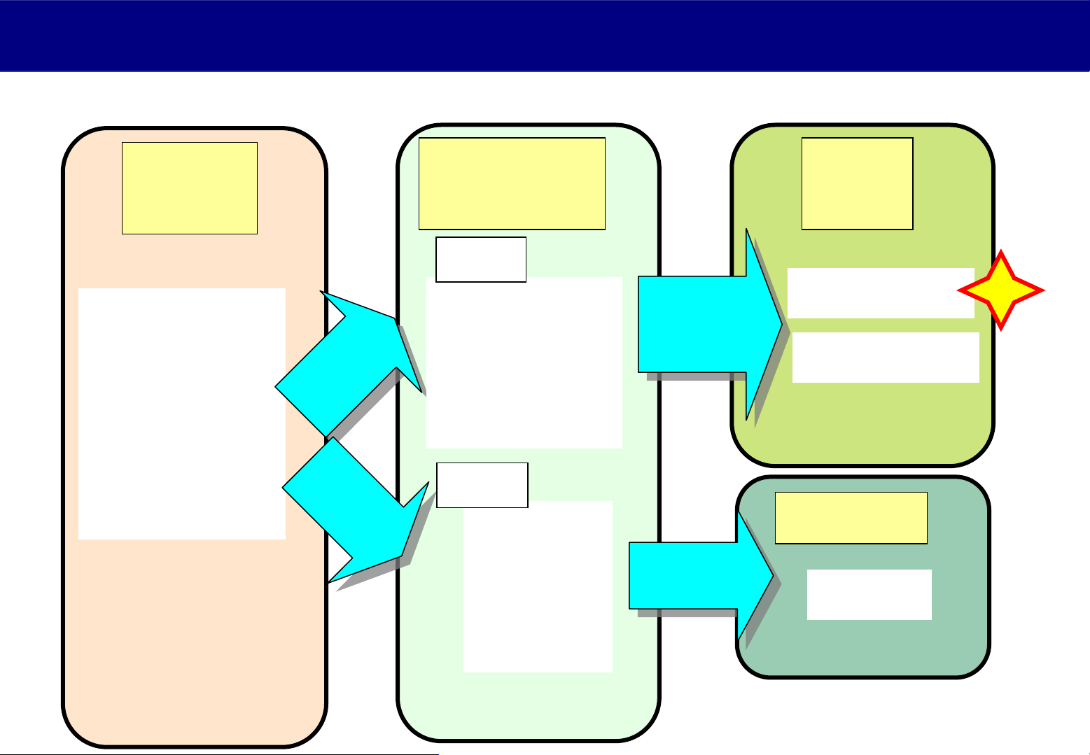
2-2.
Signal Circuit
Signal Circuit
Summary
Summary
Input
Source
TV tuner
HDMI
AV terminal
SD card
PC
Ethernet
Video
Video
Signal
Signal
Audio
Audio
Signal
Signal
Signal
Processor
Video
Brightness
Contrast
Sharpness
etc
Audio
Bass
Treble
Balance
Video /
Video /
control
control
data
data
Audio
Audio
Signal
Signal
Panel
Drive
3D Picture
2D Picture
Speaker
Sound
New
Volume
10
Page 11
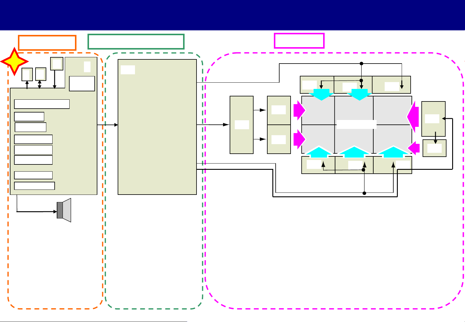
2-3.
Signal Circuit Overview
Signal Circuit Overview
Input Source
New
K
V
HDMI 1, 2, 3, 4
Tuner
PC IN
VIDEO 1/2
COMP 1/2
SD card
ETHERNET
AUDIO OUT
SPEAKER
XH
A
Power
switch
(L/R/
Woofer)
Signal Processor
D
SC
Panel Drive
SU
SD
C4
C1
Dual scan
C5
Panel
C2
C6
SS
SS2
C3
<Back view>
V : Transmitter
K : LED, Remote controller
A : AV Terminal, PC, Ethernet
Tuner,
HDMI Interface
HDMI Switch
Digital Signal processor
Systrem MPU
Peaks LDA2
XH : Additional Digital Tuner
D : Format Converter
Plasma AI,
Sub-Field Processor
SC: Scan Drive
SU: Scan Out (Upper)
SD: Scan Out (Lower)
SS: Sustain Drive
SS2: Sustain Out
C1: Data Drive (Lower Right)
C2: Data Drive (Lower Center)
C3: Data Drive (Lower Left)
C4: Data Drive (Upper Right)
C5: Data Drive (Upper Center)
C6: Data Drive (Upper Left)
11
Page 12
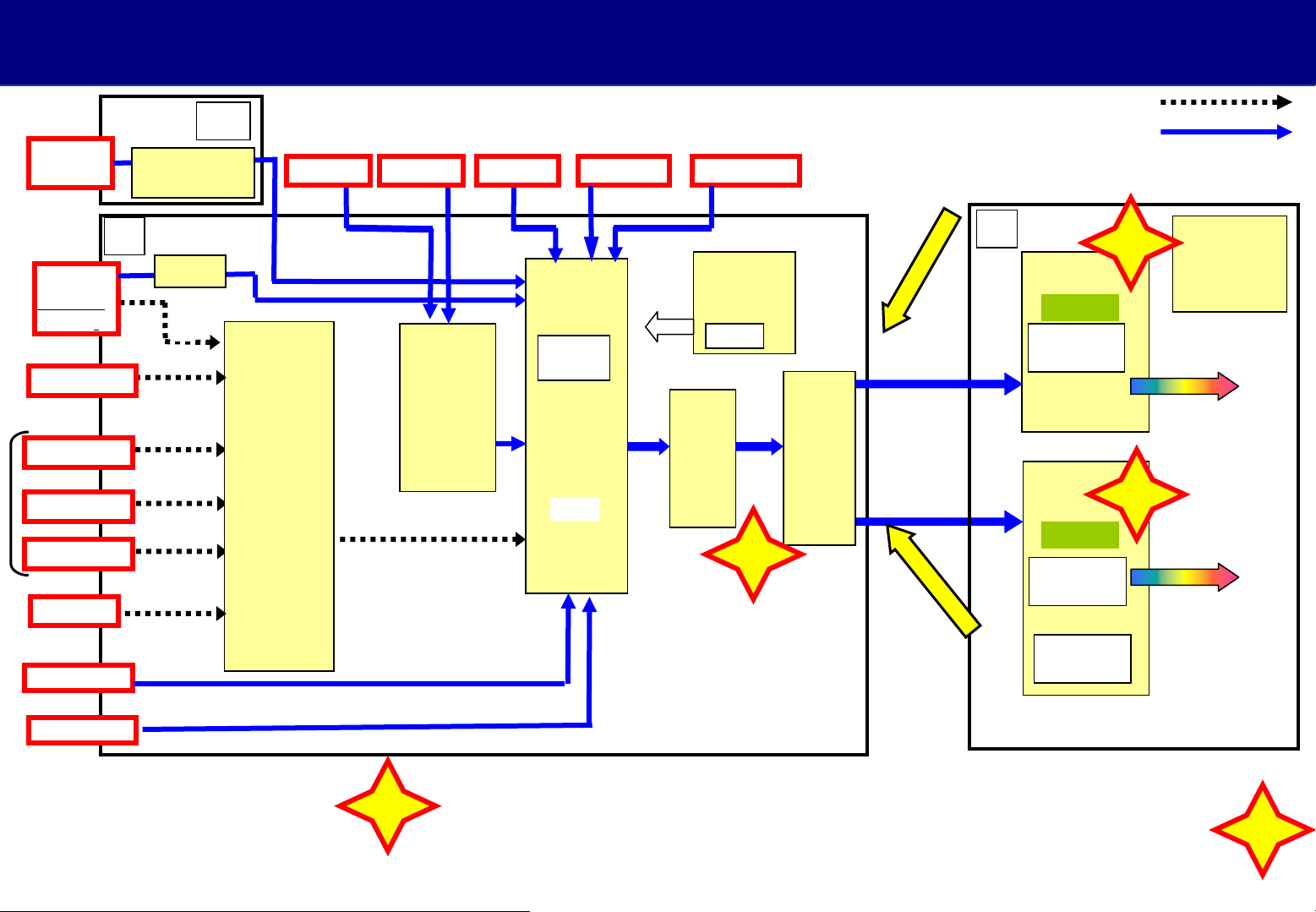
2-4.
Video signal processing
Video signal processing
TU6700/6701
Tuner
(Digital)
TU2901
Tuner
(Analog/
Digital)
JK3701
VIDEO 2
JK3000
VIDEO 1
COMP 1
COMP 2
JK3001
PC IN
JK8703
ETHERNET
JK8700
USB
IC6702
2ndFront End
Processor
A
IC8300
OFDM
V
V
Y,C / V
Y,Pb, Pr
Y,Pb,Pr
R,G,B / H,V
XH
IC3001
IC2601
SWITCH
JK4503
HDMI 1
VIDEO
JK4500 JK4501 JK4502
HDMI 2 HDMI 3
Data
IC8000
Peaks
-LDA2
Video
Signal
Processor
LOSD
Y,Pb,Pr
IC4500
HDMI
zer
Equali
& switch
HDMI 4
LVDS
Data
JK8600
SD Card
IC1100
SYSTEM
GenX8
IC4200
FRC
MPU
LVDS
Data
New
IC5800
MIHO-3D
n
o
i
t
n
e
t
t
a
LVDS Data
(right)
LVDS Data
(left)
a
t
t
e
n
t
i
o
n
D
IC9400
PD4H
Slave
DATA
Processor
Right picture
IC9300
PD4H
Master
DATA
Processor
Left picture
Discharge
control
Analog
Digital
New
New
IC9003
PANEL
MICOM
To SC
board
To C
boards
To SC
board
To C
boards
<A Board>
IC3001 : Video Switch
IC4500 : HDMI Equalizer & switch
IC1100 : System MPU
IC8300 : OFDM
nd
IC6702 : 2
Front End Processor
New
IC8000 : Video Signal Processor
IC4200 : Frame Rate Converter
IC5800 : Conversion (SBS-->FS system)
LVDS selector
<D Board>
IC9003 : Panel MICOM
IC9300 : Plasma AI, HV Sync control
New
Sub Field Processor (Left)
IC9400 : Plasma AI, H/V Sync control,
Sub Field Processor (Right)
12
Page 13
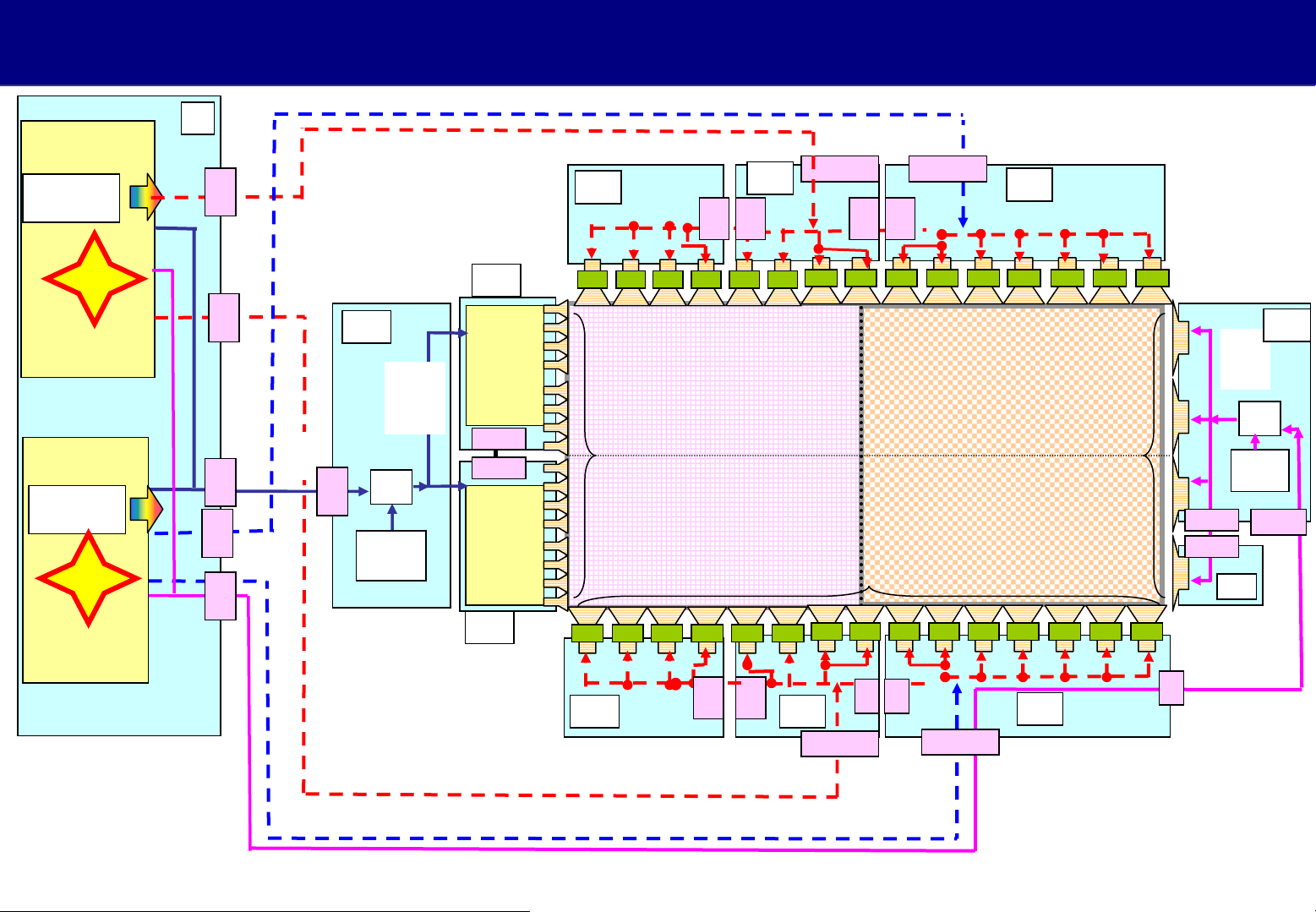
2-5.
Panel Drive
Panel Drive
IC9400
PD4H
DATA
Processor
New
Right picture
IC9300
PD4H
DATA
Processor
New
Left picture
D
D
34
D
31
D
20
D
33
D
32
SUS
CONTROL
PULSE
VIDEO
DATA
SCAN
CONTROL
PULSE
VIDEO DATA &
DATA TIMING PULSE
SC
SC
20
Voltage
Reg.
VIDEO
DATA
SCAN
Drive
Signal
ICs
SU
IC14601
IC14602
IC14603
IC14604
IC14605
IC14606
SU11
SU12
IC14801
IC14802
IC14803
IC14804
IC14805
IC14806
SD
C4
CA1 CA2
SCAN
ELECTRODE
1080 Pixel
CB1 CB2
C1
C5
C40C
50
CA3
CA4 CA5 CA6 CA7 CA8 CA9
C51 C61
C6
C56C
66
CA10 CA11CA12CA13CA14CA15
Left pictureRight picture
(1920 x 1080) (1920 x 1080)
SUSTAIN
ELECTRODE
1080 Pixel
<Back side view>
DATA ELECTRODE
1920pixel (R,G,B)
CB4 CB5 CB6 CB7 CB8 CB9CB10CB11CB12CB13CB14 CB15
CB3
C21
C26C
36
C3
C31
C
10
C
20
C2
SS21
SS24
C
33
SUS
CONTROL
PULSE
SUS
Drive
Signal
ICs
Voltage
Reg.
SS2
SS
SS33
<SU Board>
IC14601-IC14608 : SHIFT REGISTER (UPPER)
<SD Board>
IC14801-IC14808 : SHIFT REGISTER (LOWER)
13
Page 14

3. Picture Problem
14
Page 15
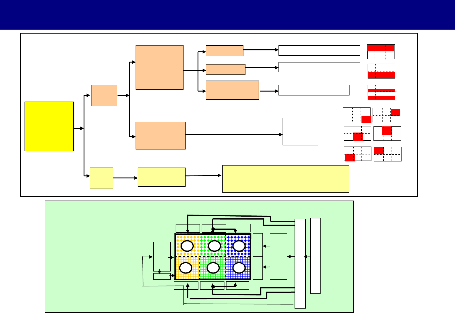
3-1.
Abnormal Picture (Sound OK)
Abnormal Picture (Sound OK)
Where
abnormal
picture
is
displayed ?
Flow of video signal
Local
Area
ALL
Area
Upper half
or
Lower half
Left / Center/
Right
Corner
All over the
screen
Upper half
Lower half
Both Lower half
and Upper half
(For checking,Test pattern is useful.)
SU Board ( or A or D or SC)
SD Board ( or A or D or SC)
SS Board ( or A or D )
C or A
or D ( or
Panel )
A or D or SC or
SS board or Panel
Right
Center
Left
(Front view)
SS
SS2
C6
C3
C5
C2
456
123
C1
C4
SU
SD
SC
A
D
15
Page 16
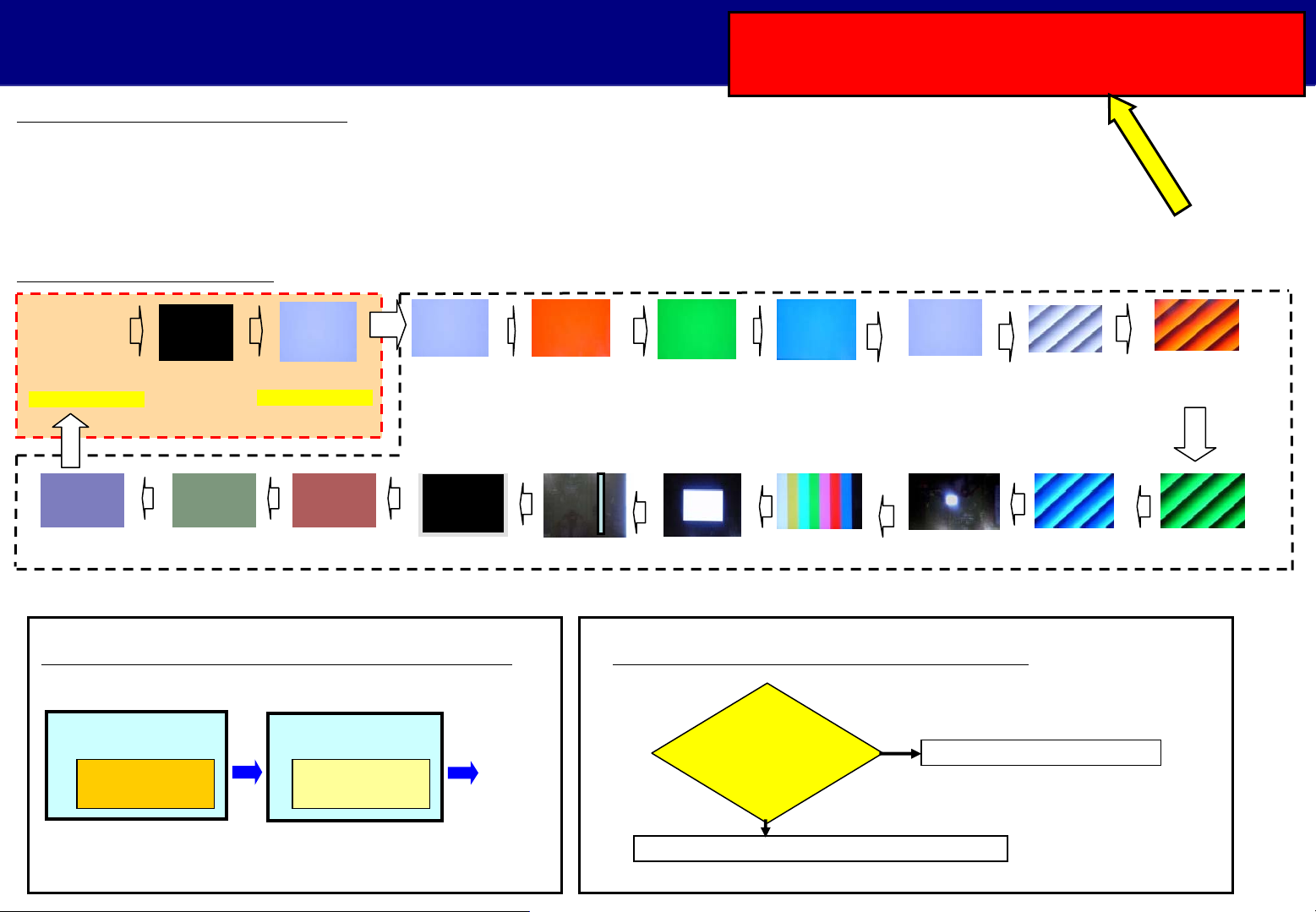
3-2. Test patterns
Not available at 3D mode condition.
Change setting mode from 3D to 2D.
How to show Test Pattern
1.Press the “VOLUME-” on the TV set and push “0” button of remote controller 3 times at the same time.
2. After this procedure, you can enter “Service Mode” and select “Aging”, then “Test pattern” will appear.
3. Push “3" button of Remote Controller to select the test pattern mode to forward.
4. Push “4“ button of Remote Controller to select the test pattern mode to reverse.
Normal Test Pattern
TIME
0
1:R/G/B/W
(with character)
2: Black
A board
(with character)
0
3:White
18:Dark red19:Dark green20:Dark blue
4:White
17:White Frame
5:Red
6:Green 7:Blue
D board
15:A and B zone16:Scrolll
8:ON/OFF Aging
9:Ramp white
12:Ramp Blue13 :1% window14:Color bar
a
t
t
e
n
t
i
o
n
10:Ramp Red
11:Ramp Green
Where are Test Patterns generated ?
A board
Test Pattern
1-3
Nos.1-3 are generated in A board and
Nos.4-20 are generated in D board.
D board
Test Pattern
Panel
4-20
How to separate defective board
Check
Test Patterns (4-20)
Abnormal
D or C board or Panel will be defective.
Normal
A board will be defective.
16
Page 17

4. Power Supply Circuit
17
Page 18

4-1. Power circuit Overview
<Block Diagram>
AC Plug
P
Fuse
Relay
Standby
Power
Circuit
Relay ON/OFF
PFC ON/OFF
FSTB_15V
STB 5V
STB ON
Q503
SW
Bias Main
Q557
SW
IC701
Q551
SW
FSTB
15V ON
Power
Power
MCU
MCU
STB_PS
F_STBY_ON
Panel_ON
A
D
IC
3.3V
Power SW
IC1100
SYSTEM
SYSTEM
MPU
MPU
PANEL_STB_ON
IC9003
Panel Micom
Panel Micom
PFC
Circuit
Power
Circuit
Q401
Q355
Vsus
Vda
15V
<Load Circuit>
n
io
t
n
e
t
t
a
Note: From power circuit, 5V is not output.
18
Page 19

4-2. Power Supply Sequence
1. AC Plug-in
AC
Plug
P
Fuse
Relay
PFC
Circuit
Standby
Power
Circuit
Relay
ON/OFF
PFC
ON/OFF
FSTB_15V
STB 5V
STB ON
Q503
Bias Main
Power
Circuit
3. TV_SUB_ON
AC
Plug
P
Fuse
Relay
PFC
Circuit
Standby
Power
Circuit
Relay
ON/OFF
PFC
ON/OFF
FSTB_15V
STB 5V
STB ON
Q503
Bias Main
Power
Circuit
Q557
SW
Q557
SW
Q551
SW
STB_PS
SW
F_STBY_15V ON
IC701
Power
Power
MCU
MCU
Q401
Q355
Q551
SW
STB_PS
SW
F_STBY_15V ON
IC701
Power
Power
MCU
MCU
Q401
Q355
F_STBY_ON
Panel
_ON
Vsus
Vda
15V
F_STBY_ON
Panel
_ON
Vsus
Vda
15V
A
3.3V
IC
D
SYSTEM
SYSTEM
MPU
IC9003
Panel
Panel
Micom
Micom
<Load Circuit>
A
3.3V
IC
D
SYSTEM
SYSTEM
MPU
IC9003
Panel
Panel
Micom
Micom
<Load Circuit>
Power SW
IC1100
MPU
PANEL STB_ON
Power SW
IC1100
MPU
PANEL STB_ON
2. Power SW ON
AC
Plug
P
Fuse
Relay
PFC
Circuit
Standby
Power
Circuit
Relay
ON/OFF
PFC
ON/OFF
FSTB_15V
STB 5V
STB ON
Q503
Bias Main
Power
Circuit
4. Panel_ON
AC
Plug
P
Fuse
Relay
PFC
Circuit
Standby
Power
Circuit
Relay
ON/OFF
PFC
ON/OFF
FSTB_15V
STB 5V
Q557
STB ON
Q503
SW
Bias Main
Power
Circuit
Q557
SW
Q551
SW
STB_PS
SW
F_STBY_15V ON
IC701
Power
Power
MCU
MCU
Q401
Q355
Q551
SW
STB_PS
SW
F_STBY_15V ON
IC701
Power
Power
MCU
MCU
Q401
Q355
F_STBY_ON
Panel
_ON
Vsus
Vda
15V
F_STBY_ON
Panel
_ON
Vsus
Vda
15V
A
3.3V
IC
D
IC
D
SYSTEM
SYSTEM
MPU
IC9003
Panel
Panel
Micom
Micom
<Load Circuit>
3.3V
SYSTEM
SYSTEM
MPU
MPU
IC9003
Panel
Panel
Micom
Micom
<Load Circuit>
Power SW
IC1100
MPU
PANEL STB_ON
Power SW
IC1100
PANEL STB_ON
19
Page 20

5. Protection Circuit
20
Page 21

5-1. Power LED blinking times table
<Check point>
Blinking
times
1
2
3
4
5
6
7
8
9
Contents Main Check Point
Unknown SOS
Panel Information SOS
Panel 15V SOS
Panel 3.3V SOS
Panel Power SOS
Panel 5V SOS
Driver SOS1
(SC Energy recovery circuit)
(D-SC FPC DET)
Driver SOS2
(SU/SD Connector DET)
(SU/SD Scan and Logic IC)
Driver SOS3
(SS FPC DET)
(SS Energy recovery circuit)
Discharge Control SOS
D Board
D Board
P Board
A Board
SC Board
D-SC FPC
SC, SU, SD Board
SS, SS2 Board
D Board
10
11
12
13
Sub 5V, Sub 3.3V, Sub 9V, Tuner Power
F15V, MIHO_3.3V, LED_8V
Fan SOS
Sound SOS
Communication error A Board
A Board, P Board,
SC Board, SS Board
A Board
Fan
A Board
Speaker
21
Page 22

5-2. Operation of Protection Circuit (1/3)
<Block Diagram for 2-8,10,12 times blinks>
P Board
Relay
Q703
Q705
IC701
8
24
PFC
MAIN
RELAY
ON/OFF
BIAS
Q366
Power
MCU
P15V
H=SOS
14
16
PANEL
PS
ON/OFF
SOS
F_STB_ON/OFF
1
L=ON
P
7
P
25
L=ON
D Board
IC9801
IC9802
D
25
A Board
A
7
TUNER
SOS
FAN
SOS
SOUND
SOS
IC9003
5 times
5V
3.3V
P5V
60
DET
2 times
P15V
62
DET
3 times
3.3V
61
DET
4 times
PS_SOS
85
Panel Main ON
75
IC1100
GenX8
52
F_STBY_ON/OFF
28
TUNER_SOS
FAN_SOS
61
27
SOUND_SOS
Panel Micom
SCAN_SOS
(SC_Floating)
SCAN_SOS
34
Panel SOS
10 times
11 times
12 times
6 times
7 times
8 times
SUS_SOS
ALARM
12
Panel
SOS
IC8000
65
68
66
PeaksLDA2
D
20
D
32
SC Board
SC
20
C3
C
31
IC16581
ERROR
DET
PC16480
Photo
COUPLER
Q16876
IC16791
Q16604
SS Board
SS
C
33
33
SS2
Green LED
(D16583)
IC16251,
ERROR
DET
Green LED
(D16253)
FFC Cable Detect
SS21
SS24
1/2 Vo
15Vf
Vscn
16Vf
Vset
Q16280
n
e
t
t
a
1/2 Vo
a
t
t
n
io
t
e
n
t
i
o
n
22
Page 23

5-2. Operation of Protection Circuit (2/3)
<Block Diagram for 10 times blinks>
F_STB_15V
P Board
A6
IC5401
IC5607
IC5501
SUB 9V
SUB 5V_Tuner
SUB 3.3V
D5522
SHORT Detection
F15V,
SUB5V
SUB9V
STB_3.3V
Q5522
A Board
A7
P
Board
SUB 3.3V
SUB 9V
SUB 5V
SUB3.3V_SENSE
35
DTV9V_SENSE
36
38
SUB5V_SENSE
28
SOS
H
52
F_STBY
_ON/OFF
L=ON
IC1100
System MPU
23
Page 24

5-2. Operation of Protection Circuit (3/3)
<Block Diagram for 12 times blinks>
P Board
AC_IN
Relay PFC
Relay OFF
IC701
8
Power MCU
24
Q355
A Board
IC2301 / IC2302
15V
A
P
6
6
D2301
SPEAKER
AMP
SUB3.3V
Q2300
A
P
7
7
1
IC1100
52
F_STBY_ON/OFF
SOUND SOS(12 times)
H
27
L
3
SOS
24
Page 25

6. Troubleshooting
of Power Supply Circuit
25
Page 26

6. Power LED No Lit
6. Power LED No Lit
Power LED Status
No Lit
Defective Block (possibility)
P, A Board ( AC Power Cord)
How to find the defective board
AC input
at 1 to 2 pin
of P9 ?
Yes
Power SW ON.
Standby 5V output
at P7’s 1 pin ?
Yes
A Board
No
No
AC power cord NG
Power source NG
P Board
or
AC Plug
Power Supply
P
P9
1
STB5V STB3.3V
2
P7
1
A
A7
1
a
t
t
e
n
t
io
n
A1
3
K
K1
STB3.3V
3
26
Page 27

6. LED 1 time blink
6. LED 1 time blink
Contents
Unknown SOS
Panel Information SOS
Defective board
In this case, the defective board is A or other board.
Defective Board
A or other board
27
Page 28

6. LED 2 times blinks
6. LED 2 times blinks
Contents Defective Board ( Possibility )
Panel 15V SOS D Board ( A, P, SC,SS )
Defective board
The defective board is D or A or P or SC or SS board.
Power Supply / Protection Circuit
15V is also connected to A, SC and SS boards.
n
o
i
t
n
e
t
t
a
P
AC_IN
Relay PFC
Relay OFF
IC701
8
Power MCU
24
P7 5
+15V
14
1
P25
1
2
9
D
D25
1
2
PANEL_MAIN_ON/OFF
9
A
14
+15V
F_STBY_ON/OFF
52
IC9003
t
62
75
IC1100A7
a
15V DET
12
PANEL_SOS
34
n
o
i
t
n
e
t
28
Page 29

6. LED 3 times blinks
6. LED 3 times blinks
Contents
Panel 3.3V SOS
Defective Board (Possibility)
D board ( A, C )
Defective board
In this case, the defective board is D or A or C1-C6 board.
Power Supply / Protection Circuit
3.3V is also connected to C1-C6 boards.
P
AC_IN
Relay PFC
Relay OFF
IC701
8
Power MCU
24
P7 5
+15V
14
1
P25
1
2
9
D
D25
1
2
PANEL_MAIN_ON/OFF
9
A
A7
F_STBY_ON/OFF
14
IC5501
3.3V
52
61
75
IC1100
IC9003
3.3V DET
12
PANEL_SOS
34
n
o
i
t
n
e
t
t
a
n
o
i
t
n
e
t
t
a
29
Page 30

6. LED 4 times blinks
6. LED 4 times blinks
Contents
Power SOS
P board (C1, C2, C3, C4,C5, C6 Board)
Defective Board (possibility)
Power Supply / Protection Circuit
P65, C4, C5 and C6 are omitted in this block diagram.
P
PFC
Relay
8
24
Relay OFF
IC701
2016
Power MCU
1
5P7
Vsus
Vsus
Power
Supply
SOS
16
14
Vda
a
P2
1
P11
P35
1
2
e
t
t
P25
12
9
n
o
i
t
n
D25
12
9
A7
14
SC2
SS11
C35
1
2
D
PS_SOS
PANEL_MAIN_ON/OFF
A
F_STBY_ON/OFF
n
o
i
t
n
e
t
t
a
How to find the defective board
SC
1
SS
11
C3
C36
16
20
C26
5
1
52
C2
85
75
C36
37
40
IC9003
PS SOS
12
PANEL_SOS
34
IC1100
C1
C26
4
1
Disconnect SS11
connector.
Power SW ON,
Vsus output at pin 1 at
P11 connector
before shutdown?
Yes
Disconnect C35 connector.
Power SW ON.
Vda output at P35’s 1,2 pin
before Shutdown ?
Yes
C3,C2, C1 Board (*1)
(*1) In the same way, by disconnecting C65 connector
and checking P65’s 1,2 pin,
C4,C5,C6 and P board can be separated.
No (VSUS NG)
P Board
No (Vda NG)
P Board
30
Page 31

6. LED 5 times blinks
6. LED 5 times blinks
Contents
Panel 5.0V SOS
Defective Board (possibility)
D Board ( SC, SS Board )
Power Supply / Protection Circuit
C4,C5 and C6 are omitted in this block diagram.
P
AC_IN
Relay PFC
15V
SC
SC20
35
CB
CB
CB4CB5CB
CB
2
1
3
C10C
20
Panel
CB
6
7
C2C1
C21
CB8CB9CB10CB11CB12CB
C26C
36
C3
C31
13
CB14CB
1
n
How to find the defective board
o
i
t
n
e
t
t
a
SS
SS33
SS2
15
C
33
Check without AC power input.
1
Disconnect D20.
D20’s 1pin
Short with GND?
Yes
D Board
Disconnect SC20.
SC20’s 35pin
Short with GND?
Disconnect
No
D20 and D32.
D32’s 68pin
Short with GND?
D Board
No
Yes
No
SS Board
Relay OFF
IC701
8
Power
24
MCU
D20
D
1
2
11
A7
14
IC9801
A
P25
1
2
14
1
5P7
11
D25
1
o
i
t
n
e
t
t
a
5V
PANEL_MAIN_ON/OFF
F_STBY_ON/OFF
D32
68
n
PANEL SOS
IC1100
52
IC9003
60
P5V DET
75
GenX8
12
34
Yes
SC Board
31
Page 32

6. LED 6 times blinks
6. LED 6 times blinks
Contents
Defective Board (Possibility)
SC Energy recovery circuit SOS
Power Supply / Protection Circuit
P
AC_IN
Relay
IC701
8
24
Relay
OFF
Power
MCU
1
PFC
14
Vsus
+15V
P2
P11
P25
1
2
9
1
15V
15V
1
D20
30 29 1
D25
1
2
IC9801
9
SC2
1
SC20
6
7
5V
35
21
15
PANEL_MAIN_ON/OFF
SC Board (D, P )
SC
15V
Buffer
SOS
SS11
1
Vscn Reg.
Vad Reg.
Energy Recovery Circuit
SS
SOS
PANEL_SOS
FET
Driver
IC9003
65
75
Output
FET
SOS DET
SC SOS
12
Vfo
Vf
How to find the defective board
SU
Check without AC power input.
SD
D
Check connection of SC20 and D20.
Check 15V line
Check 5V line.
Short with ground or not.
n
o
i
t
n
e
t
t
a
When SC20 is disconnected,
6 times blinking continues.
5P7
A7
14
F_STBY_ON/OFF
IC1100
52
34
32
Page 33

6. LED 7 times blinks
6. LED 7 times blinks
Contents
Defective Board
How to find the defective board
SC Floating voltage SOS
Power Supply / Protection Circuit
P
15V
15V
P5V
AC_IN
Vsus
Relay
IC701
8
24
Relay
OFF
Power
MCU
1
PFC
5P7
14
+15V
P25
D20
30 29 1
A25
1
1
2
2
+5V
9
9
A7
14
F_STBY_ON/OFF
PANEL_MAIN_ON/OFF
SC, SU, SD board
SC
SC20
6
7
35
20
Scan Control
15V
Buffer
SOS
16
SOS
52
Vscn Reg.
Vad Reg.
5Vf
Vscn
16Vf
Vset
Q16875,79
IC9003
68
Voltage SOS
75
PANEL_SOS
IC1100
Vfo
PC16480
Q16867
PC16791
SC Floating
12
34
Vf
Remove both
SU and SD. (*1)
No
SU,SD Board
en
on
ti
SU
Connect SC Jig to
SC50 connector.
And Power ON.
Power LED blinks?
att
SD
Yes
SC Board
IMPORTANT
(*1) How to remove both SU and SD.
After discharging perfectly, remove 4 screws (VFG)
and 3 connectors (SU41, SD42 and SD46) all.
att
en
on
ti
If not, some boards will be damaged
when power is ON.
CAUTION: Before connecting, discharge perfectly.
A
SC JIG (TZSC09187)
SU41
SD46
SD42
SC50
VFG
33
After checking, remove SC JIG.
n
o
i
t
n
e
t
t
a
Page 34

6. LED 8 times blinks
6. LED 8 times blinks
Contents
SS Energy recovery circuit SOS
Power Supply / Protection Circuit
SC
P
AC_IN
Relay
IC701
8
24
Relay
OFF
Power
MCU
1
5P7
Vsus
PFC
14
+15V
P2
1
P11
1
4
P25
D25
1
2
9
A7
14
SC2
SC20
D20
1
+15V
2
9
A
Vsus
1
P5V
35
C3
C36
1
3
1
D32
+5V
PANEL_MAIN_ON/OFF
F_STBY_ON/OFF
Defective Board (possibility)
SS, SS2 board ( D, P )
C1,C2, C4,C5 and C6 are omitted in this block diagram.
How to find the defective board
FFC
No (VSUS NG)
Power SW ON.
VSUS output at
P11’s 1 pin before
Shutdown?
Yes
(SS Pulse NG)
D Board
FFC
CAUTION: Before connecting, discharge perfectly.
When FFC is disconnected,
8 times blinking continues.
C
31
SS
SS11
1
4
SS33
1
C33
1
7
7
16
6863
SOS
Vsus
+15V
Energy Recovery
Buffer
52
FET
Driver
SOS DET
SOS
FFC DET
IC9003
66
Recovery SOS
75
PANEL_SOS
IC1100
Circuit
Output
FET
SS Energy
12
34
SS
SS
SS22
SS2
D
Disconnect SS11.
Power SW ON.
VSUS output at
P11’s 1 pin
before Shutdown ?
Yes
SS or SS2 Board
Remove SS2.
Power On.
Yes
SS2
Board
att
No
en
No
SS Board
on
ti
P
Board
34
Page 35

6. LED 9 times blinks
6. LED 9 times blinks
<Contents and Defective Board>
Contents
Discharge control SOS
<Defective board>
In this case, the defective board is D board.
Defective Board
D Board
35
Page 36

6. LED 10 times blinks
6. LED 10 times blinks
Contents
Defective Board ( possibility )
Regulator voltage SOS (*1)
Power Supply / Protection Circuit
P
PFC
Relay
IC701
Power
AC_IN
Vsus
Vda
15V
Relay
OFF
8 24
MCU
1
P11
4
P25
1
2
P6
1
2
3 3
7
9
P7
5
15V
D25
1
2
A6
1
2
7
9
A7
14
a
15V
A
F15V
t
t
e
n
D
att
15V
t
i
o
en
n
on
ti
IC5401
IC5607
IC5501
SUB 9V
SUB 5V
A Board ( P, SC, SS )
*1 Sub 5V, Sub 3.3V, Sub 9V, Tuner Power(5V), F15V, MIHO_3.3V, LED 8V
D5522
Q5522
STB3.3V
SUB 3.3V
SUB 9V
SUB 5V
35
SUB3.3V
37
SUB9V
38
SUB5V
SOS
28
H
F_STB
ON/OFF
52
IC1100
D20
29
30
SS11
SC20
SS
15V
4
SC
6
15V
7
How to find the defective board
After Power SW ON,
F_STB 15V outputs
at P6’s pin 9
15V outputs at
P6’s pin 1
before Shutdown?
Yes
A Board
No
P Board
36
Page 37

6. LED 11 times blinks
6. LED 11 times blinks
Contents
FAN SOS
Defective Board (possibility)
A Board (FAN )
Power Supply / Protection Circuit
P
Vsus
Vda
15V
PFC
Relay
IC701
Power
T501
AC_IN
Relay OFF
8 24
MCU
1
STB_5V
P6
7
9
P7
5
F_STB_15V
A6
8
9
A7
14
A
F_15V
F_STB_ON/OFF
IC5740
Vin Vout
2
IC1100
52
3
61
GenX5
FAN SOS
How to find the defective board
on
ti
en
att
No
All Fan stop?
A Board
A8
Yes
FAN A
Fan Volt
SOS
FAN B
Fan Volt
SOS
FAN C
Fan Volt
SOS
FAN D
Fan Volt
SOS
FAN (Check each fan.)
37
Page 38

6. LED 12 times blinks
6. LED 12 times blinks
P
PFC
Relay
8 24
IC701
Power
MCU
15V
IC
Relay
OFF
1
Contents
SOUND SOS
Defective Board (possibility)
A Board ( P, SC, SS )
Power Supply / Protect Circuit
P11
15V
4
P25
P6
P7
A25
1
1
2
2
A6
15V
1
1
2
2
8
7
9
9
F_STB_15V
A7
15V
A
D
D2301
SUB3.3V
Q2301
IC2301/IC2302
23,24
43,44
SPEAKER
L
3
AMP
SOS
D20
29
30
att
SS11
en
4
SC20
6
7
on
ti
How to find the defective board
SS
15V
SC
15V
Check without AC power input.
After Power SW ON,
15V comes up ?
A Board
Disconnect SC20.
Check pin 6 is
short with GND?
Yes
Yes
No
Check without AC power input.
No
Disconnect P11.
SS11’s pin 4
Short with GND?
Yes
SS Board
P Board
No
T501
AC_IN
F_STB
_15V
14
5
IC1100
GenX8
F_STB ON/OFF
52
27
H
SC Board
38
Page 39

6. LED 13 times blinks
6. LED 13 times blinks
<Contents and Defective Board>
Contents
Communication Error between IC8000 and IC1100
<How to find the defective boards>
In this case, the defective board is A board.
Defective Board
A Board
39
Page 40

7. Service Information
40
Page 41

7-1. How to find problem of TV and 3D Eyewear
n
o
i
t
n
te
When both of TV and 3D Eyewear are on-site or at workshop.
t
a
Check output of
1
2D picture.
OK
Check 3D Eyewear
2
Battery.
OK
Check shutter
3
operation of 3D Glass.
Both TV and 3D Eyewear is OK
Note: 3D setting
<VIErA TOOLS>
NG
NG
NG
Check IR output from TV
3D Eyewear Problem
[ 3Dsettings ]
Select
TV Problem
3D Blu-ray Disc Player
If it playbacks 1080P signal, player is OK.
Change to New Battery.
Then, confirm again.
NG
3D Eyewear Problem
OK
NG
TV Problem
OKOK
<3Dsettings Picture>
Look
<Top menu>
[Setup]
Selection
<Setup display>
※Displayed at left-top ※Displayed at left-top
[3D setting]
Selection
※Displayed at left-top
41
Page 42

7-2. Checking of 3D Eyewear
1. Battery voltage check
Battery voltage
More than 2.5V
Normal charge is indicated when the power switch is turned on
and the Power LED turns on for 2 seconds.
If the Power LED blinks for 5 times after the power is turned on,
the battery voltage is low.
Look
Less than 2.5V
- If the Power LED blinks for 3 times after the power is turned on,
please push Power button again.
- When the voltage of Microprocessor IC under 2V, the power
doesn't turn on.
- The IR receiving distance is shortened when the power-supply
voltage decreases.
2. Shutter operation check
Check shutter open/close operation by changing 2D/3D select switch
on the user menu.
The liquid crystal shutter open/close timing is controlled by receiving IR
signals from the TV, which provide 3D expression of the images.
1. Change the switch to 3D and 2D, repeatedly.
2. Glass color is changed to dark and bright by detecting a Shutter
On/Off signal from TV if they are working propely.
IR
IR
Power Button Power LED
Look
3D Auto 3D 2D
Look
TV outputs IR signal from 2 positions.
Even if one IR signal is blocked, the 3D
eyewear will receive the other IR signal.
2D : Shutter Off
3D : Shutter On 2D : Shutter Off
(After 5 sec.)
42
Page 43

7-3. How to check IR signal from TV set
Set the 3D/2D select switch on the user menu to 3D to confirm the IR
output signal from the TV by using Mobile Phone’s Camera.
n
io
t
n
e
t
t
a
Note: The camera with IR cut filter cannot be used.
3D Auto 3D 2D
10/12
Look
There are total six IR output LED.
Mobile Phone’s
camera
LED are indicated if TV is working propery.
2D : IR Output OFF
2D : IR Output OFF
3D : IR Output ON
Look
2D → 3D
3D : IR Output ON
43
Page 44

4. Self check of TV
77--4. Self check of TV
1. How to access
Self check indication only:
While pressing [Volume(-)] button of the TV set, press [OK] button of the remote control
for more than 3 seconds.
Self check indication and factory shipping setting
While pressing [Volume(-)] button of the TV set, p
for more than 3 seconds.
Access method is same as 2009 models
2. Screen display and Check Point
Screen display ( e.g. Europe PAL model)
ress [MENU] button of the remote control
Look
Check Point
3. Exit
Disconnect AC cord from wall outlet.
China, Hong Kong
44
Page 45

5. How to enter into Service Mode
77--5. How to enter into Service Mode
While pressing [Volume(-)] button of the TV set, press [0] button of the
remote control three times within 2 second
Picture adjustment
White balance adjustment
Option setting
New
VSUS
Aging
Service tool
s.
Screen display (e.g. Europe PAL model)
Key command
“1” button --- Main items Selection in forward direction
“2” button --- Main items Selection in reverse direction
“3” button --- Sub items Selection in forward direction
“4” button --- Sub items Selection in reverse direction
“VOL” button --- Value of sub items change in forward direction (+), in reverse direction (-).
45
Page 46

6. Electronic adjustment of
77--6. Electronic adjustment of
Vsus
Vsus
●New Function
Previously, adjustment of VSUS was done by the volume on P board by digital voltmeter.
From 2010, electronic adjustment of VSUS is adopted.
By this function, Vsus is adjusted without opening back cover and without using digital voltmeter.
●
Operation procedure
●
Operation procedure
1. Select VSUS Adj. (VSUS adjustment menu) of Service mode.
1. Select VSUS Adj. (VSUS adjustment menu) of Service mode.
2. By selecting ““OKOK””
2. By selecting
VSUS adjustment menu can be entered.
VSUS adjustment menu can be entered.
key of VSUS adjustment menu by remote control,
key of VSUS adjustment menu by remote control,
●Flow of Vsus adjustment (Service mode)
Service mode
VSUS
“Return”
VSUS
TEST LOW
Low
“OK”
・Display ON/OFF = ”5”key
“Volume (-)”
“Volume (+)”
VSUS
TEST HIGH
Vsus Adj. mode
This mode sets “-5V” of actual Vsus adjusted value.
And, by this condition, it is adjusted by that condition.
(How to adjust)
By “Vsus Low test”, check “White pattern”.
1.
2-1. When there is not “Non-lit cell”,
by “3” key , go to “Conf.mode”.
2-2. When there is “Non-lit cell”,
move to “Vsus test High”.
After confirming that there is not “Non-lit cell”
by White pattern again, by “OK” key,
go to
When there is still “Non-lit cell”,
panel is defective.
“Conf.mode”.
New
n
io
t
n
e
t
t
a
White
pattern
VSUS
CONF LOW
“OK”
VSUS
Low
“3 ”“4 ”
(Vsus adjustment
value decision)
“4 ”
VSUS
CONF HIGH
“OK”
VSUS
HIGH
“3 ”
Conf. mode
By pushing “OK” key by this mode,
“actual VSUS adjusted value” is set.
(How to adjust)
1. By
2-1.
2-2.
“Conf.mode”, check White pattern.
When there is no problem, by “OK” key,
adjustment is completed.
When there is problem, by “4 “ key,
back to “Vsus Adj.mode” and adjust Vsus again.
46
Page 47

7.
77--7.
Mirror function
Mirror function
●New Function
When there is a defective of Vertical line ((
by this function in video processing part of A board,
by this function in video processing part of A board,
video signal becomes mirror reversed and vertical line (hor
video signal becomes mirror reversed and vertical line (hor
So, panel is diagnosed to be normal or not.
So, panel is diagnosed to be normal or not.
At the repairing job site, diagnosis can
At the repairing job site, diagnosis can
be done without opening the back cover.
be done without opening the back cover.
●
Operation procedure
●
Operation procedure
S
ervice mode Æ
ervice mode
S
●
Diagnosis
●
Diagnosis
Vertical line shifts. Æ A board (Signal processing circuit) is failure.
Vertical line shifts.
Mirror function
Mirror function
ÆON
Horizontal line
Horizontal line
New
)
,
)
,
izontal line) shifts.
izontal line) shifts.
00: Default, OFF
01: Right and left mirror-reversed.
02: Up and down mirror-reverse d .
MIRROR function adjust menu
Vertical line does not shift. → Panel is failure.
Vertical
line
failure
MIRROR Function ON
(Mirror reversed)
Look
Mirror
reversed
Vertical line moves.
Æ A board (Signal processing circuit)failure.
47
Page 48

8. Functions of SRV--
77--8. Functions of SRV
Tool
Tool
There are 4 functions of SRV (Service)-TOOL as follows.
Same as 2009 models
(1) Power SOS (LED blinking) history
(2) Power ON time & Count
(3)Memory Editor
Memory Editor
Please check the “PTCT”
Previous SOS
Latest SOS
PTCT: 04, 01, 00, 04, 01
Numbers are not decimal but hexadecimal.
decimal: 1,2,3,4,5,6,7,8,9,10,11, 12, 13, - - hexadecimal: 1,2,3,4,5,6,7,8,9, a, b, c, d, - - -
How to display ‘Power ON time & Counter’
1.Move the cursor to the lower right corner.
2.Press ‘Mute’ button of remote control (5sec).
How to display ‘Memory Editor’
1.Move the cursor to the upper right corner.
2.Press ‘Mute’ button of remote control (5sec).
Second previous SOS
Time : 00006 : 40
Count : 0000082
First SOS after shippingSecond SOS after shipping
Hour
Minute
times
n
io
t
n
e
t
t
a
(4)Local Maintenance
Local Maintenance
Note: Generally, do not use Memory editor !!
How to display ‘Local Maintenance’
1.Move the cursor to the upper left corner.
2.Press ‘OK’ button of remote control (5sec).
48
Page 49

9.
77--9.
Data Copy by SD Card
Data Copy by SD Card
(1. From TV set to SD card 2. From SD card to TV set)
(1. From TV set to SD card 2. From SD card to TV set)
①Copy of setting data when exchanging repair board ( A board)
Same as 2009 models
PDP
(Before exchanging)
Setting data to SD Card
(Available data for Copy)
・Customer setting data
A
(After exchanging)
Copied setting data
to repaired board
SD
・Channel scanned data
・Adjustment data / shipping data
②Copy of hotel mode setting data
PDP
Master set
Copy setting data
to SD card
SD
【Preparation】 Make pwd file of ① or ② in SD card. (Make new (empty) text file and change file name.)
①For exchanging repair board・・・ boardreplace.pwd
②For hotel mode setting ・・・ hotel.pwd
(Same type model) (Same type model) (Same type model)
Data Copy Data Copy Data Copy
■■■
(Available data for Copy)
Setting by using data of SD card
・Customer setting data
・Channel scanned data
(pwd File name)
Wrong example:
Boardreplace.pwd
BOARDRELACE.PWD
Hotel.pwd
n
io
t
n
e
t
t
a
Note: Keep one pwd file in SD card. If there are several files in one SD card, it is NOT likely to work.
a
tten
【Action】 : Power On TV set. >
1.From TV set to SD card
2.From TV set to SD card
Insert SD card. > Input pass word.
For exchanging repair board hotel mode setting
2770 4850
2771 4851
ti
o
n
49
Page 50

10.
77--10.
Wireless LAN (Wi--
Wireless LAN (Wi
Fi)
Fi)
Panasonic Dongle can be used.
Panasonic Dongle
-11a(5GHz), 11b(2.4GHz), 11g(2.5GHz),
11n(5GHz/2.4GHz) are available.
11n (5GHz) is good for AV transmission.
- To use Wi-Fi, setting of access point is necessary.
Note:
1. Connecting and disconnecting Dongle when TV is ON
-Connecting Dongle to USB terminal is OK.
-Disconnecting Dongle is not good.. (TV will hung up.)
2. Same dongle
-Using in other TV is OK.
-When TV is OFF, disconnecting and connecting is OK without setting.
-When TV is OFF and dongle is disconnected and other dongle is connected,
re-setting is necessary.
Finding problem of dongle and TV set
① AP Setting of Network setup
Insert dongle into TV set. And when display of “AP Setting”
becomes “No adapter”, dongle is NG.
attenti
on
attenti
Network Setup
on
a
New
i
t
n
e
t
t
Dongle is not
Connected.
USB
terminal
n
o
Dongle is connected.
Look
Network setting
(e.g. wired)
Wired or Wireless
Wireless network setting
(e.g. Connection error)
② Check connection status of wireless LAN
When indication of AP setting is “Connected”, setting status
of access point is confirmed.
When setting status is not good, re-setting will be necessary.
③ Check dongle only.
There is the diagnostic software for checking only dongle.
By using PC, it can be checked.
Vol.1 site
Downloaded Software
Software
50
Page 51

11.
77--11.
Other
Other
USB
USB
functionss
function
1. USB HDD recording
New
- Only Direct recording (1 time speed)
- Only digital broadcasting program recording
(Copy controlled contents, analogue broadcasting
program and source from external input are not available.)
TV set and HDD are bound by the generated key in A board.
--TV set and HDD are bound by the generated key in A board.
Contents by HDD can be watched only by the recorded TV.
--Contents by HDD can be watched only by the recorded TV.
HDD for this purpose can not be used by PC.
--HDD for this purpose can not be used by PC.
When self--
--When self
done, registered information in HDD becomes reset and
done, registered information in HDD becomes reset and
recorded contents
recorded contents
check (TV ““--””
check (TV
by USB HDD can not be
by USB HDD can not be
key + Remote control ““
key + Remote control
watched.
watched.
Menu””
Menu
2. USB Keyboard
- To input letters for VIErA cast
- Wire and wireless keyboards are supported.
3. USB Flash Memory and USB-HUB
- USB Flash memory (Data is loaded by PC.)
Contents Note
Still
Picture
Moving
Picture
Music
- USB-HUB: To use Communication camera and so on.
JPEG
SD VIDEO Standard quality MPEG2-PS
AVCHD FULL-HD quality H.264-TS
DivX HD Only LDA2 model
MP3 WMP and ripping of iTunes
AAC Ripping of iTunes
Not available in somecountries
Available
key) is
key) is
a
t
t
e
n
ti
Look
USB HDD recording
Only Australia, New Zealand
and Hong Kong models.
USB Cable
AC adapter
(MUST)
at
t
ent
USB-HDD
USB Keyboard
o
n
Wire and wireless keyboards are supported.
(Wireless keyboard by USB dongle type is supported.)
Extended keys are not supported.
USB Flash Memory and USB- HUB
USB 1
USB 2
( Communication camera ,
HDD、Flash )
i
on
How to check USB Keyboard, Flash Memory, USB-HUB
Connect the troubled USB keyboard, USB flash memory,
and USB-HUB to PC and check them by PC.
a
t
te
n
t
i
o
AC adaptor
n
(MUST)
51
 Loading...