

Page 1
ORDER NO. ITD0207025C2
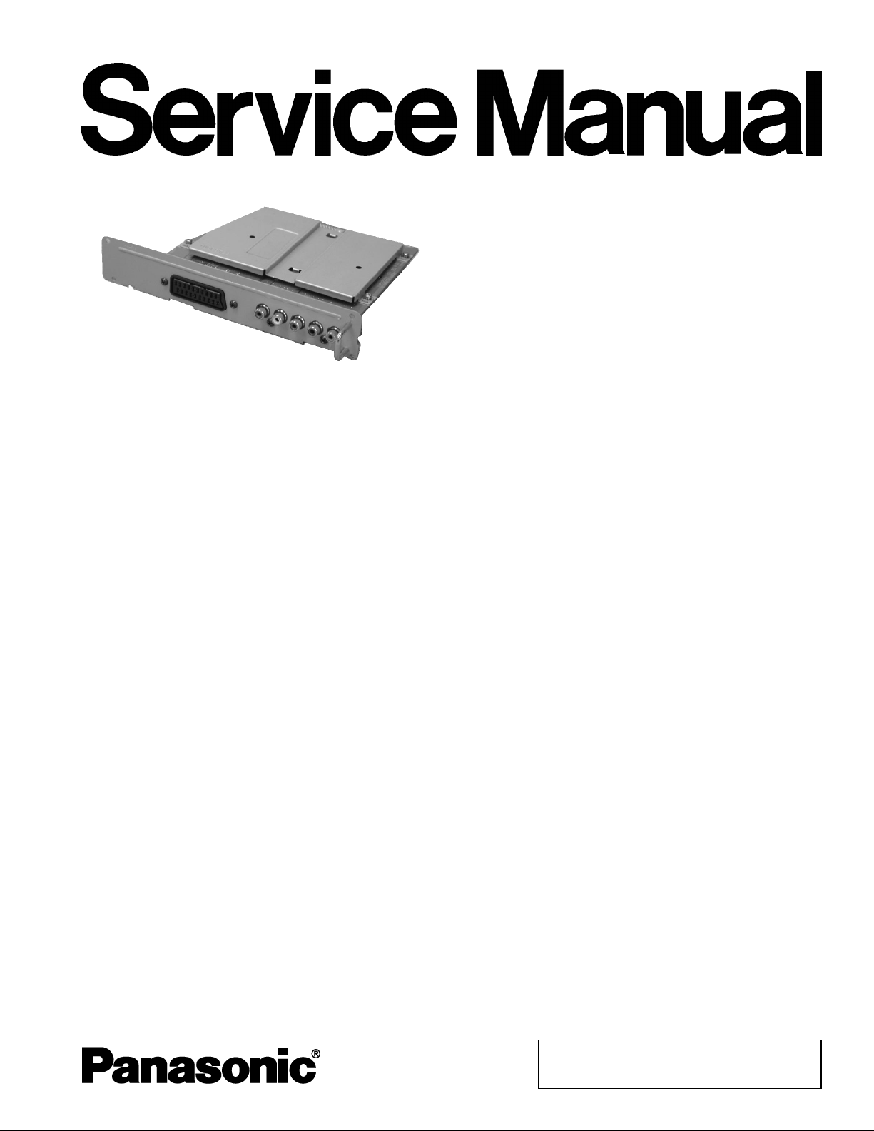
Scart/Component Terminal Board
TY-42TM5T
TY-37TM5T
© 2002 Matsushita Electric Industrial Co., Ltd. All
rights reserved. Unauthorized copying and
distribution is a violation of law.
Page 2
TY-42TM5T / TY-37TM5T
CONTENTS
1 Prevention of Electro Static Discharge (ESD) to
Electrostatically Sensitive (ES) Devices
2 About lead free solder (PbF)
3 Conductor Views
3.1. HT-Board (TY-37/42TM5T)
4 Block and Schematic Diagrams
4.1. Schematic Diagram Notes
Page Page
4.2. HT-Board (TY-37/42TM5T) Block Diagrams
3
4
5
5
7
7
4.3. HT-Board (1 of 2) (TY-37/42TM5T) Schematic Diagrams
4.4. HT-Board (2 of 2) (TY-37/42TM5T) Schematic Diagrams
5 Replacement Parts List
5.1. Replacement Parts List Notes
5.2. Replacement Parts List
10
11
11
12
8
9
2
Page 3
TY-42TM5T / TY-37TM5T
1 Prevention of Electro Static Discharge (ESD) to
Electrostatically Sensitive (ES) Devices
Some semiconductor (solid state) devices can be damaged easily by static electricity. Such components commonly are called
Electrostatically Sensitive (ES) Devices. Examples of typical ES devices are integrated circuits and some field-effect transistors and
semiconductor "chip" components. The following techniques should be used to help reduce the incidence of component damage
caused by electro static discharge (ESD).
1.Immediately before handling any semiconductor component or semiconductor-equipped assembly, drain off any ESD on your
body by touching a known earth ground. Alternatively, obtain and wear a commercially available discharging ESD wrist strap,
which should be removed for potential shock reasons prior to applying power to the unit under test.
2.After removing an electrical assembly equipped with ES devices, place the assembly on a conductive surface such as alminum
foil, to prevent electrostatic charge buildup or exposure of the assembly.
3.Use only a grounded-tip soldering iron to solder or unsolder ES devices.
4.Use only an anti-static solder removal device. Some solder removal devices not classified as "anti-static (ESD protected)" can
generate electrical charge sufficient to damage ES devices.
5.Do not use freon-propelled chemicals. These can generate electrical charges sufficient to damage ES devices.
6.Do not remove a replacement ES device from its protective package until immediately before you are ready to install it. (Most
replacement ES devices are packaged with leads electrically shorted together by conductive foam, alminum foil or comparable
conductive material).
7.Immediately before removing the protective material from the leads of a replacement ES device, touch the protective material
to the chassis or circuit assembly into which the device will be installed.
Caution
Be sure no power is applied to the chassis or circuit, and observe all other safety precautions.
8.Minimize bodily motions when handling unpackaged replacement ES devices. (Otherwise hamless motion such as the brushing
together of your clothes fabric or the lifting of your foot from a carpeted floor can generate static electricity (ESD) sufficient to
damage an ES device).
3
Page 4
TY-42TM5T / TY-37TM5T
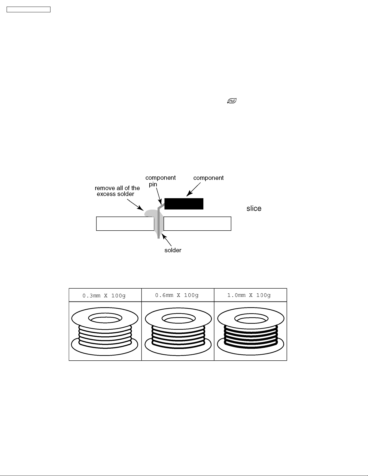
2 About lead free solder (PbF)
Note: Lead is listed as (Pb) in the periodic table of elements.
In the information below, Pb will refer to Lead solder, and PbF will refer to Lead Free Solder.
The Lead Free Solder used in our manufacturing process and discussed below is (Sn+Ag+Cu).
That is Tin (Sn), Silver (Ag) and (Cu) although other types are available.
This model uses Pb Free solder in it’s manufacture due to environmental conservation issues. For service and repair work, we’d
suggest the use of Pb free solder as well, although Pb solder may be used.
PCBs manufactured using lead free solder will have the PbF within a leaf Symbol
Caution
·Pb free solder has a higher melting point than standard solder. Typically the melting point is 50 ~ 70 ーF (30~40ーC) higher.
Please use a high temperature soldering iron and set it to 700 ± 20 ーF (370 ± 10 ーC).
·Pb free solder will tend to splash when heated too high (about 1100 ーF or600ーC).
If you must use Pb solder, please completely remove all of the Pb free solder on the pins or solder area before applying Pb
solder. If this is not practical, be sure to heat the Pb free solder until it melts, before applying Pb solder.
·After applying PbF solder to double layered boards, please check the component side for excess solder which may flow onto
the opposite side. (see figure below)
Suggested Pb free solder
There are several kinds of Pb free solder available for purchase. This product uses Sn+Ag+Cu (tin, silver, copper) solder.
However, Sn+Cu (tin, copper), Sn+Zn+Bi (tin, zinc, bismuth) solder can also be used.
stamped on the back of PCB.
4
Page 5

3 Conductor Views
3.1. HT-Board (TY-37/42TM5T)
HT-BOARD (FOIL SIDE)
6
TXNHT10MKS (FOR TY-42TM5T)
TXNHT10NJS (FOR TY-37TM5T)
TY-42TM5T / TY-37TM5T
A24
A25 A1
B24
B25
5
R4607
C4603
C4604
C4608
C4607
C4606
C4605
R4608
H1
C4609
C4610
C3703
C3318
C4612
C4611
C3709
A2
A1
B2
B1
C3733
JS3305
C3317
JS3301
A20
A19
B20
B19
H2
A2
B2
B1
JS3311
HT
4
R3311
R3312
R3316
R3313
4
R3314
R3309
R3310
R3308
C3316
85
IC3699
1
C3718
C3724
C3732
C3705
C3741
R3729
C3731
C3708
R3716
C3734
C3706
C3702
C3716
C3715
C3714
C3725
C3727
C3726
3
1
SEE REVERSE FOR ORDER NO.
R3528
JS3312
R3433
R3562R3570
JS3309
R3434
R3561
TNPA2552
AV2
R
L
JK3103JK3104
BR
GR
AV1
R3529
R3502
R3501
21
20
R3530
2
JS3307
1
2
JS3308
R3304
R3303
R3503
C3302
JK3102
1
TY-42TM5T HT-BOARD TXNHT10MKS
TY-37TM5T HT-BOARD TXNHT10NJS
TY-42TM5T HT-BOARD TXNHT10MKS
TY-37TM5T HT-BOARD TXNHT10NJS
ABCDEFGH I
5
Page 6

TY-42TM5T / TY-37TM5T
6
HT-BOARD (COMPONENT SIDE)
TXNHT10MKS (FOR TY-42TM5T)
TXNHT10NJS (FOR TY-37TM5T)
C3319
JS3313
JS3314
R3320
JS3310
R3319
A2
A1
B2
R3315
B1
R3321
5
TS3301 TS3302
HD
VD
TNPA2552
R3537
ORDER
NO.
4
1
HT
3
PbF
R3462
R3464
2
GR
R3534
C3510
Q3501
C3507
IC3501
R3526
R3532
C3511
Q3502
R3523
R3520
R3517
C3508
C3505
IC3502 IC3503
R3514
C3554
R3563
4
5
3
1
Q3461
R3463
R3465
R3466
C3461
R3461
JK3103
B
Q3504
R3522
R3559
R3519
B
IC3551
R3557
C3551
R3516
C3504
R3513
NP
R3535
C3512
C3509
R3554
R3538
Q3503
L3583
C
R3553
C3581
R3564
Q3505
R3524
R3521
C3553
R3555
NP
R3518
C3506
R3515
5
13
R3556
C3584
R3551
A20
H2
A19
B20
B19
C3308
C3310
L3702
A
C3710
R3712
R3560
C3558
IC3552
R3571
5
4
1
R3566
R3567
R3568
R3558
NP
C3552
C3586
L3582
R3552
C3583
C3582
AV2
RL R
R3715
L3581
C3717
R3569
C3557
C3723
4
3
R3565
C3305
R3318
C3721
R3317
C3585
NP
C3701
IC3553
L3424
C3707
L3304
C3720
Q3422
R3430
C3424
C3728
R3427
JK3104
C3713
R3714
R3453
R3432
R3428
C3430
C3428
C3432
JS3306
C3712
C3722
R3424
C3313
C3729
R3422
R3423
Q3421
R3429
L3703
C3711
R3713
R3425
C3431
A1
B1
C3730
R3431
A2
B2
R3426
C3422
C3742
R3711
C3719
R3721
R3717
C3740
C3426
L3422
JS3303
X3701
65
80
C3739
R3452
C3704
R3451
NPNP
R3421
R3444
64
1
C3738
IC3441
R3447
R4612
R4611
L3701
C3322
C3429
Q3442
R3445
C3737
C3444
C3443
C3743
C3321
C3445
IC3701
C3736
L3442
IC4601
R3709
C3735
5
1
R3710
C3745
C3744
R3441
56
1
18
1
R3525
Q3441
R3705
R3727
4
3
R3449
R3442
H1
R3413
R3450
R3703
R3704
R3707
R3724
R3531
R3446
R3414
R3723
C
R3443
R3706
R3722
LC3501
R3448
R3504
C3442
Q3701
R3702
A24
R3708
41
R3725
1
3
R3510
24
C3746
R3701
3
A25
B25B24
R4605
25
4
R3728
TS3501
10
5
4
C4602
C4618
29
C4617
28
R4604
C4616
40
C3314
R3307
R3306
C3304
1
L3303
IC3702
5
R3540
18
1
9
5
1
3
R3505
R3511
C3501
C3502
NP
C3441
L3441
21
20
L4603
L4602
C4614C4615
L4601
C3303
C4613
L3305
1
8
R3305
IC3305
8
C3312
C3307
14
R4557
R3718
R3719
R3720
LC3502
10
1
4
3
R3507
B
R3506
C3503
NP
JK3102
AV1
L3301
C3315
5
4
TS3502
9
R3512
NP
L3302
R3541
1
C3311
16
9
5
18
A
R3509
R3508
C3320
IC3699
R3527
C3306
C3309
R3533
Q3402
C3412
JS3302
R3404
1
8
R3412
L3404
LC3503
R3536
R3407
C3408
R3410
C3410
R3408
R3402
R3539
C3404
NP
Q3506
Q3401
C3411
R3403
L3402
H0
R3542
10
TS3503
9
JS3304
R3411
R3405
R3406
R3409
C3406
R3401
NP
C3409
C3402
1
2
Parts Location
IC
IC3305 E-4
IC3501 E-2
IC3502 D-2
IC3503 D-2
IC3551 B-3
IC3552 B-3
IC3553 C-3
IC3699 E-3
IC3701 D-4
IC3702 D-3
IC4601 D-5
HT-BOARD (COMPONENT SIDE)
TRANSISTOR
Q3401 E-2
Q3402 E-2
Q3421 C-3
Q3422 C-3
Q3441 D-2
Q3442 C-2
Q3461 A-2
Q3501 D-2
Q3502 D-2
Q3503 E-2
Q3504 D-2
Q3505 E-2
Q3506 E-2
TP
TS3301 B-5
TS3302 B-5
TS3501 D-3
TS3502 E-3
TS3503 F-3
1
TY-42TM5T HT-BOARD TXNHT10MKS
TY-37TM5T HT-BOARD TXNHT10NJS
TY-42TM5T HT-BOARD TXNHT10MKS
TY-37TM5T HT-BOARD TXNHT10NJS
ABCDEFGH I
6
Page 7

4 Block and Schematic Diagrams
4.1. Schematic Diagram Notes
Important Safety Notice
Components identified by mark have special characteristics important for safety.
When replacing any of these components, use only manufacture's specified parts.
Notes:
1. Resistor
All resistors are cabon 1/4W resistor, unless marked as follows:
Unit of resistance is OHM [W] (K=1,000, M=1,000,000).
: Nonflammable : Metal Oxide
: Solid : Metal Film
: Wire Wound : Fuse:
2. Capacitor
All capacitors are ceramic 50V capacitor, unless marked as follows:
Unit of capacitance is mF, unless otherwise noted.
: Temperature Compensation : Electrolytic
: Polyester : Bipolar
M
m T
: Metalized Polyester : Dipped Tantalum
: Polypropylene : Z-Type
3. Coil
Unit of inductance is mF, unless otherwise noted.
4. Test Point
: Test Point position
5. Earth Symbol
: Chassis Earth (Cold) : Line Earth (Hot)
6. Voltage Measurement
Voltage is measured by a DC voltmeter.
Conditions of the measurement are the following:
Power Source ................................................... AC 120V, 50/60Hz
Receiving Signal ............................................... Colour Bar signal (RF)
All customer's controls ...................................... Maximum positions
7. Number in red circle indicates waveform nember.
(See waveform pattern table.)
8. When arrow mark ( ) is found, connection is easily found from the direction of arrow
NP
+
-
Z
(North America model)/AC220-240V,
50/60Hz (Except North America)
TY-42TM5T / TY-37TM5T
Remarks:
1. The Power Circuit contains a circuit area which uses a separate power supply to isolate the
earth connection.
The circuit is de fined by HOT and COLD indications in the schematic diagram. Take the
follwing precautions.
All circuits, except the Power Circuit, are cold.
Precautions
a. Do not touch the hot part or the hot and cold parts at the same time or you may
be shocked.
b. Do not short- circuit the hot and cold circuits or a fu se may blow and parts may
break.
c. Do not connect a n instrument, such as an oscilloscope, to th e hot and cold
circuits simulta neously or a fuse may blow.
Connect the earth of instruments to the earth connection of the circuit being
measured.
d. Make sure to disconnect the pow er plug before removing the chassis.
2. Following diodes are interchangeable.
MA150- MA162 (Replacement part)
9. Indicates the major signal flow. : Video Audio
10. This schematic diagram is the latest at the time of printing and subject to change without
notice.
TY-37TM5T/TY-42TM5T
Schematic Diagram Notes
TY-37TM5T/TY-42TM5T
Schematic Diagram Notes
7
Page 8

TY-42TM5T / TY-37TM5T
4.2. HT-Board (TY-37/42TM5T) Block Diagrams
TY-37TM5T/TY-42TM5T HT-Board Block Diagrams TY-37TM5T/TY-42TM5T HT-Board Block Diagrams
8
Page 9

4.3. HT-Board (1 of 2) (TY-37/42TM5T) Schematic Diagrams
TY-42TM5T / TY-37TM5T
TY-37TM5T/TY-42TM5T HT-Board(1of2)Schematic Diagrams TY-37TM5T/TY-42TM5T HT-Board(1of2)Schematic Diagrams
9
Page 10

TY-42TM5T / TY-37TM5T
4.4. HT-Board (2 of 2) (TY-37/42TM5T) Schematic Diagrams
TY-37TM5T/TY-42TM5T HT-Board(2of2)Schematic Diagrams TY-37TM5T/TY-42TM5T HT-Board(2of2)Schematic Diagrams
10
Page 11

5 Replacement Parts List
5.1. Replacement Parts List Notes
TY-42TM5T / TY-37TM5T
11
Page 12

TY-42TM5T / TY-37TM5T
5.2. Replacement Parts List
Ref.
No.
C3302 ECJ1XC1H101J C 100PF, J, 50V 1
C3303-05ECJ1XF1C104Z C 0.1UF, Z, 16V 3
C3306 EEVHB1C101P E 100UF, 16V 1
C3307 EEVHB0J101 E 100UF, 6.3V 1 EEVHB0J101P
C3308 EEVHB1C470 E 47UF, 16V 1
C3309 EEVHB1C101P E 100UF, 16V 1
C3310 EEVHB1C470 E 47UF, 16V 1
C3311-14ECJ1XF1C104Z C 0.1UF, Z, 16V 4
C3315 ECJ2VF1C105Z C 1UF, Z, 16V 1
C3316 TCUY0J685MBM C 6.8UF, 6.3V 1 F1K0J685A003
C3317-21ECJ2VF1C104Z C 0.1UF, Z, 16V 5
C3322 EEVHB1C470 E 47UF, 16V 1
C3402 ECJ1XC1H561J C 560PF, J, 50V 1
C3404 ECJ1XC1H561J C 560PF, J, 50V 1
C3406 ECJ1XC1H561J C 560PF, J, 50V 1
C3408 ECJ1XC1H561J C 560PF, J, 50V 1
C3409,10EEVHP1C100R E 10UF, 16V 2
C3411,12ECJ2VF1C105Z C 1UF, Z, 16V 2
C3422 ECJ1XC1H561J C 560PF, J, 50V 1
C3424 ECJ1XC1H561J C 560PF, J, 50V 1
C3426 ECJ1XC1H561J C 560PF, J, 50V 1
C3428 ECJ1XC1H561J C 560PF, J, 50V 1
C3429,30EEVHP1C100R E 10UF, 16V 2
C3431,32ECJ2VF1C105Z C 1UF, Z, 16V 2
C3441,42ECJ2XB1E104K C 0.1UF, K, 25V 2
C3443 EEVHB1C470 E 47UF, 16V 1
C3444 ECJ2VF1H103Z C 0.01UF, Z, 50V 1
C3445 ECJ2VF1C104Z C 0.1UF, Z, 16V 1
C3461 EEVHB1C470 E 47UF, 16V 1
C3501-03EEVHP0J470 E 47UF, 6.3V 3
C3504-09ECJ2VF1C104Z C 0.1UF, Z, 16V 6
C3510-12ECJ2VF1H103Z C 0.01UF, Z, 50V 3
C3551,52EEVHP0J470 E 47UF, 6.3V 2
Part No. Part Name &
Description
Pcs Remarks
Ref.
No.
C3733 ECJ2VF1H104Z C0.1UF,Z,50V 1
C3734 ECJ2VF1H683Z C 0.068UF, Z, 50V 1
C3738-40ECJ2XF1H224Z C 0.22UF, Z, 50V 3 ECJ2VF1H224Z
C3741 ECJ2XB1E104K C0.1UF,K,25V 1
C3743 ECJ2XC1H391J C390PF,J,50V 1
C3744 ECJ2XB1H152K C 1500PF, K, 50V 1
C3745 ECJ2XF1H224Z C 0.22UF, Z, 50V 1 ECJ2VF1H224Z
C3746 ECJ2VF1C104Z C0.1UF,Z,16V 1
C4603 ECJ1XB1H102K C 1000UF, Z, 50V 1
C4604 ECJ1XB1C104K C0.1UF,Z,16V 1
C4605 ECJ1XB1H102K C 1000UF, Z, 50V 1
C4606 ECJ1XB1C104K C0.1UF,Z,16V 1
C4607 ECJ1XB1H102K C 1000UF, Z, 50V 1
C4608 ECJ1XB1C104K C0.1UF,Z,16V 1
C4609 ECJ1XB1H102K C 1000UF, Z, 50V 1
C4610 ECJ1XB1C104K C0.1UF,Z,16V 1
C4611 ECJ1XB1H102K C 1000UF, Z, 50V 1
C4612 ECJ1XB1C104K C0.1UF,Z,16V 1
C4613-15EEVHB1C470 E 47UF, 16V 3
C4616-18ECJ1XB1C104K C0.1UF,Z,16V 3
H0 TJSF12608 8P CONNECTOR 1 K1KA08A00138
H1 K1KB50B00030 50P CONNECTOR 1
H2 K1KB40B00015 40P CONNECTOR 1
IC3305 JLC1562BF MOS IC (MICON LSI) 1 C0JBAZ001265
IC3501-03C0ABGB000001 IC 3
IC3551-53C0ABGB000001 IC 3
IC3699 TVRJ760 IC 1
IC3701 C1AB00001345 IC 1
IC3702 PST9142NR IC (LOGIC) 1 C0EBH0000095
IC4601 C0ZBZ0000684 IC 1
JK3102 K1FB121B0009 CONNECTOER 1
JK3103 K2HA306B0049 JACK 1
JK3104 K2HA204B0097 JACK 1
JS3301-14ERJ3GEY0R00 M 0 OHM, 1/16W 14
Part No. Part Name &
Description
Pcs Remarks
C3553,54ECJ2VF1C104Z C 0.1UF, Z, 16V 2
C3557 EEVHP0J470 E 47UF, 6.3V 1
C3558 ECJ2VF1C104Z C 0.1UF, Z, 16V 1
C3702 ECJ2XB1H473K C 0.047UF, K, 50V 1
C3703 ECJ2XC1H030C C 3PF, C, 50V 1
C3704 EEVHB1C100 E 10UF, 16V 1
C3705 ECJ2VF1H683Z C 0.068UF, Z, 50V 1
C3706 ECJ2XB1H152K C 1500PF, K, 50V 1
C3708 ECJ2VF1H104Z C 0.1UF, Z, 50V 1
C3709 ECJ2XC1H030C C 3PF, C, 50V 1
C3711 ECJ2XB1H473K C 0.047UF, K, 50V 1
C3713 EEVHB0J470 E 47UF, 6.3V 1
C3714 ECJ2XC1H391J C 390PF, J, 50V 1
C3715 ECJ2XB1H152K C 1500PF, K, 50V 1
C3716 ECJ2XF1H224Z C 0.22UF, Z, 50V 1 ECJ2VF1H224Z
C3718 ECJ2VF1H683Z C 0.068UF, Z, 50V 1
C3719 ECJ2XC1H102K C 1000PF, K, 50V 1
C3722 ECUV1C684KBM C 0.68UF, Z, 50V 1 ECJ3VB1C684K
C3724 ECJ2VF1H683Z C 0.068UF, Z, 50V 1
C3725 ECJ2XC1H391J C 390PF, J, 50V 1
C3726 ECJ2XB1H152K C 1500PF, K, 50V 1
C3727 ECJ2XF1H224Z C 0.22UF, Z, 50V 1 ECJ2VF1H224Z
C3728,29EEVHB1C470 E 47UF, 16V 2
C3730,31ECJ2XB1H473K C 0.047UF, K, 50V 2
C3732 ECJ2XB1H152K C 1500PF, K, 50V 1
L3302-04ELKE103FA NOISE FILTER 3
L3305 G1C100KA0008 INDUCTOR COIL 1
L3402 ELJNA1R5JF INDUCTION COIL 1
L3404 ELJNA1R5JF INDUCTION COIL 1
L3422 ELJNA1R5JF INDUCTION COIL 1
L3424 ELJNA1R5JF INDUCTION COIL 1
L3441 TLK20LFA223M EMI FILTER 1 J0HABB000003
L3442 TLK20LFA224M EMI FILTER 1 J0HABB000004
L3701 ELKE103FA NOISE FILTER 1
L3703 ELKE103FA NOISE FILTER 1
L4601-03ELKE103FA NOISE FILTER 3
LC3501-03TAX10079 FILTER 3 J0E7904B0002
Q3401,022SD601A TRANSISTOR 2 2SD0601A
Q3421,222SD601A TRANSISTOR 2 2SD0601A
Q3441,422SD601A TRANSISTOR 2 2SD0601A
Q3461 2SD601A TRANSISTOR 1 2SD0601A
Q3501-032SD601A TRANSISTOR 3 2SD0601A
Q3504-062SB709A TRANSISTOR 3 2SB0709A
12
Page 13

Ref.
No.
R3303 ERJ6ENF1802 M 18KOHM, 1/10W 1
R3304 ERJ6ENF9101 M 9.1KOHM, 1/10W 1
R3308 ERJ3GEYJ103 M 10KOHM,J,1/16W 1
R3309,10ERJ3GEYJ220 M 22 OHM,J,1/16W 2
R3311 ERJ3GEYJ103 M 10KOHM,J,1/16W 1
R3314 ERJ3GEYJ103 M 10KOHM,J,1/16W 1
R3315 ERJ6GEY0R00 M 0 OHM,J,1/10W 1
R3317,18TAJAAH0101JV M 100 OHM,J,1/16W 2 D0GB101JA006
R3320,21ERJ6GEY0R00 M 0 OHM,J,1/10W 2
R3401,02ERJ6GEYJ561 M 560 OHM,J,1/10W 2
R3403,04ERJ6GEYJ333 M 33KOHM,J,1/10W 2
R3405 ERJ6GEYJ153 M 15KOHM,J,1/10W 1
R3406 ERJ6GEYJ333 M 33KOHM,J,1/10W 1
R3407 ERJ6GEYJ153 M 15KOHM,J,1/10W 1
R3408 ERJ6GEYJ333 M 33KOHM,J,1/10W 1
R3409,10ERJ6GEYJ101 M 100 OHM,J,1/10W 2
R3411,12ERJ6GEYJ102 M 1KOHM,J,1/10W 2
R3421,22ERJ6GEYJ561 M 560 OHM,J,1/10W 2
R3423,24ERJ6GEYJ333 M 33KOHM,J,1/10W 2
R3425 ERJ6GEYJ153 M 15KOHM,J,1/10W 1
R3426 ERJ6GEYJ333 M 33KOHM,J,1/10W 1
R3427 ERJ6GEYJ153 M 15KOHM,J,1/10W 1
R3428 ERJ6GEYJ333 M 33KOHM,J,1/10W 1
R3429,30ERJ6GEYJ101 M 100 OHM,J,1/10W 2
R3431,32ERJ6GEYJ102 M 1KOHM,J,1/10W 2
R3441 ERJ6ENF75R0 M 75 OHM, 1/10W 1
R3442 ERJ3GEYJ153 M 15KOHM,J,1/16W 1
R3443 ERJ3GEYJ333 M 33KOHM,J,1/16W 1
R3444 ERJ3GEYJ123 M 12KOHM,J,1/16W 1
R3445 ERJ3GEYJ682 M 6.8KOHM,J,1/16W 1
R3446,47TAJAAH0101JV M 100 OHM,J,1/16W 2 D0GB101JA006
R3448,49ERJ3GEYJ102 M 1KOHM,J,1/16W 2
R3453 TAJAAH0101JV M 100 OHM,J,1/16W 1 D0GB101JA006
R3461 ERJ3GEYJ102 M 1KOHM,J,1/16W 1
R3462 ERJ3GEYJ123 M 12KOHM,J,1/16W 1
R3463 ERJ3GEYJ682 M 6.8KOHM,J,1/16W 1
R3464 TAJAAH0101JV M 100 OHM,J,1/16W 1 D0GB101JA006
R3465 ERJ3GEYJ102 M 1KOHM,J,1/16W 1
R3466 TAJAAH0101JV M 100 OHM,J,1/16W 1 D0GB101JA006
R3501-03ERJ6ENF75R0 M 75 OHM, 1/10W 3
R3504 ERJ6GEYJ103 M 10KOHM,J,1/10W 1
R3505 ERJ6GEYJ332 M 3.3KOHM,J,1/10W 1
R3506 ERJ6GEYJ103 M 10KOHM,J,1/10W 1
R3507 ERJ6GEYJ332 M 3.3KOHM,J,1/10W 1
R3508 ERJ6GEYJ103 M 10KOHM,J,1/10W 1
R3509 ERJ6GEYJ332 M 3.3KOHM,J,1/10W 1
R3510-12ERJ6GEYJ220 M 22 OHM,J,1/10W 3
Part No. Part Name &
Description
Pcs Remarks
TY-42TM5T / TY-37TM5T
Ref.
No.
R3537-39ERJ6GEYJ331 M 330 OHM,J,1/10W 3
R3540-42ERJ6GEYJ471 M 470 OHM,J,1/10W 3
R3551,52ERJ6ENF75R0 M 75 OHM, 1/10W 2
R3553 ERJ6GEYJ103 M 10KOHM,J,1/10W 1
R3554 ERJ6GEYJ332 M 3.3KOHM,J,1/10W 1
R3555 ERJ6GEYJ103 M 10KOHM,J,1/10W 1
R3556 ERJ6GEYJ332 M 3.3KOHM,J,1/10W 1
R3557,58ERJ6GEYJ220 M 22 OHM,J,1/10W 2
R3561,62ERJ6GEY0R00 M 0 OHM,J,1/10W 2
R3563,64ERJ6GEYJ271 M 270 OHM,J,1/10W 2
R3565 ERJ6ENF75R0 M 75 OHM, 1/10W 1
R3566 ERJ6GEYJ103 M 10KOHM,J,1/10W 1
R3567 ERJ6GEYJ332 M 3.3KOHM,J,1/10W 1
R3568 ERJ6GEYJ220 M 22 OHM,J,1/10W 1
R3570 ERJ6GEY0R00 M 0 OHM,J,1/10W 1
R3571 ERJ6GEYJ271 M 270 OHM,J,1/10W 1
R3708,09TAJAAH0101JV M 100 OHM,J,1/16W 2 D0GB101JA006
R3711 TAJAAH0101JV M 100 OHM,J,1/16W 1 D0GB101JA006
R3713 ERJ3GEYJ103 M 10KOHM,J,1/16W 1
R3714 TAJAAH0101JV M 100 OHM,J,1/16W 1 D0GB101JA006
R3716 ERJ3GEY0R00 M 0 OHM, 1/16W 1
R3718 ERJ3GEYJ330 M 33 OHM,J,1/16W 1
R3721 ERJ6ENF75R0 M 75 OHM, 1/10W 1
R3722-24TAJAAH0101JV M 100 OHM,J,1/16W 3 D0GB101JA006
R3725 ERJ3GEYJ103 M 10KOHM,J,1/16W 1
R3727 ERJ3GEYJ101 M 100 OHM,J,1/16W 1 D0GB101JA002
R3728 ERJ3GEYJ103 M 10KOHM,J,1/16W 1
R4557 ERJ3GEYJ102 M 1KOHM,J,1/16W 1
R4604,05ERJ3GEYJ330 M 33 OHM,J,1/16W 2
R4607 ERJ3GEYJ103 M 10KOHM,J,1/16W 1
R4608 ERJ3GEYJ472 M 4.7KOHM,J,1/16W 1
R4611,12EXB38V472J RESISTOR ARRAY 2
RTL TXNHT10MKS CIRCUIT BOARD HT 1 TY-42TM5T
RTL TXNHT10NJS CIRCUIT BOARD HT 1 TY-37TM5T
X3701 H0J202500003 CRYSTAL 1
Part No. Part Name &
XTV3+10J SCREW 4
XYN3+F8 SCREW 4
K2RD093E0001 RGB21P/RCA PLAG 1
TPCB13111 CARTON BOX 1 TY-42TM5T
TPCB13113 CARTON BOX 1 TY-37TM5T
TPDF0726 PARTITION 1
TPEH161 AIR MAT 1
TQBC0499 INSTRUCTION BOOK 1
TQBC7062 INSTRUCTION SEET 1
XZBT6506 POLY BAG 1
THEL023Z SCREW 4
TQE6691 POLY BAG 1
Description
MISCELLANEOUS
Pcs Remarks
R3513-15ERJ6ENF4301 M 4.3KOHM, 1/10W 3
R3516-18ERJ6ENF5621 M5.62KOHM, 1/10W 3
R3519-21ERJ6GEYJ331 M 330 OHM,J,1/10W 3
R3522-24ERJ6GEYJ122 M 1.2KOHM,J,1/10W 3
R3525-27ERJ6ENF2210 M 221 OHM, 1/10W 3
R3528-30ERJ6GEYJ152 M 1.5KOHM,J,1/10W 3
R3534-36ERJ6ENF2210 M 221 OHM, 1/10W 3
13
 Loading...