

Page 1
ORDER NO.PCZ1602027CE
LED TV
Model No. TX-58DX750B
TX-58DX750E
TX-58DX750F
LA67 Chassis
© Panasonic Corporation 2016.
Unauthorized copying and distribution is a violation
of law.
Page 2

TABLE OF CONTENTS
PAG E PAG E
1 Safety Precautions -----------------------------------------------3
1.1. General Guidelines ----------------------------------------3
1.2. Touch-Current Check--------------------------------------3
2Warning--------------------------------------------------------------4
2.1. Prevention of Electrostatic Discharge (ESD)
to Electrostatically Sensitive (ES) Devices ----------4
2.2. About lead free solder (PbF) ----------------------------5
3 Service Navigation------------------------------------------------6
3.1. PCB Layout --------------------------------------------------6
4 Specifications ------------------------------------------------------7
5 Technical Descriptions------------------------------------------9
5.1. Specification of KEY for CI PLUS, DTCP-IP,
HDCP2.2, NETFLIX, WIDEVINE, ONE-TOONE, DIMORA and FREETIME------------------------9
5.2. USB HDD Recording --------------------------------------9
5.3. How to connect and disconnect for A15 and
A16 connectors on A board --------------------------- 10
6 CS Maintenance Menu----------------------------------------- 11
6.1. How to enter into CS Maintenance Menu ---------- 11
6.2. Repack------------------------------------------------------ 11
6.3. EDID Clock ------------------------------------------------ 12
6.4. USB HDD Drive Check --------------------------------- 12
6.5. White Balance Adjustment----------------------------- 13
6.6. System Information -------------------------------------- 14
6.7. Hotel mode------------------------------------------------- 15
6.8. Data Copy by USB Memory --------------------------- 16
7 Troubleshooting Guide---------------------------------------- 19
7.1. Check of the IIC bus lines------------------------------ 19
7.2. Power LED Blinking timing chart --------------------- 20
7.3. LCD Panel test mode ----------------------------------- 20
8 Disassembly and Assembly Instructions --------------- 21
8.1. Disassembly Flow Chart for the Unit ---------------- 21
8.2. Disassembly Procedure for the Unit----------------- 22
8.3. Countermeasure of Sound vibration
specification ----------------------------------------------- 30
8.4. P-Board Barrier ------------------------------------------- 35
8.5. Spacer-------------------------------------------------------36
8.6. A-Board radiation of heat specifications------------ 37
8.7. Specification of EMI countermeasures ------------- 42
9 Measurements and Adjustments -------------------------- 45
9.1. Voltage chart of P-board-------------------------------- 45
9.2. Voltage chart of A-board------------------------------- 45
10 Block Diagram --------------------------------------------------- 47
10.1. Block Diagram (1/2) ------------------------------------- 47
10.2. Block Diagram (2/2) ------------------------------------- 48
11 Wiring Connection Diagram --------------------------------- 49
11.1. Wiring Diagram -------------------------------------------49
11.2. Caution statement.--------------------------------------- 50
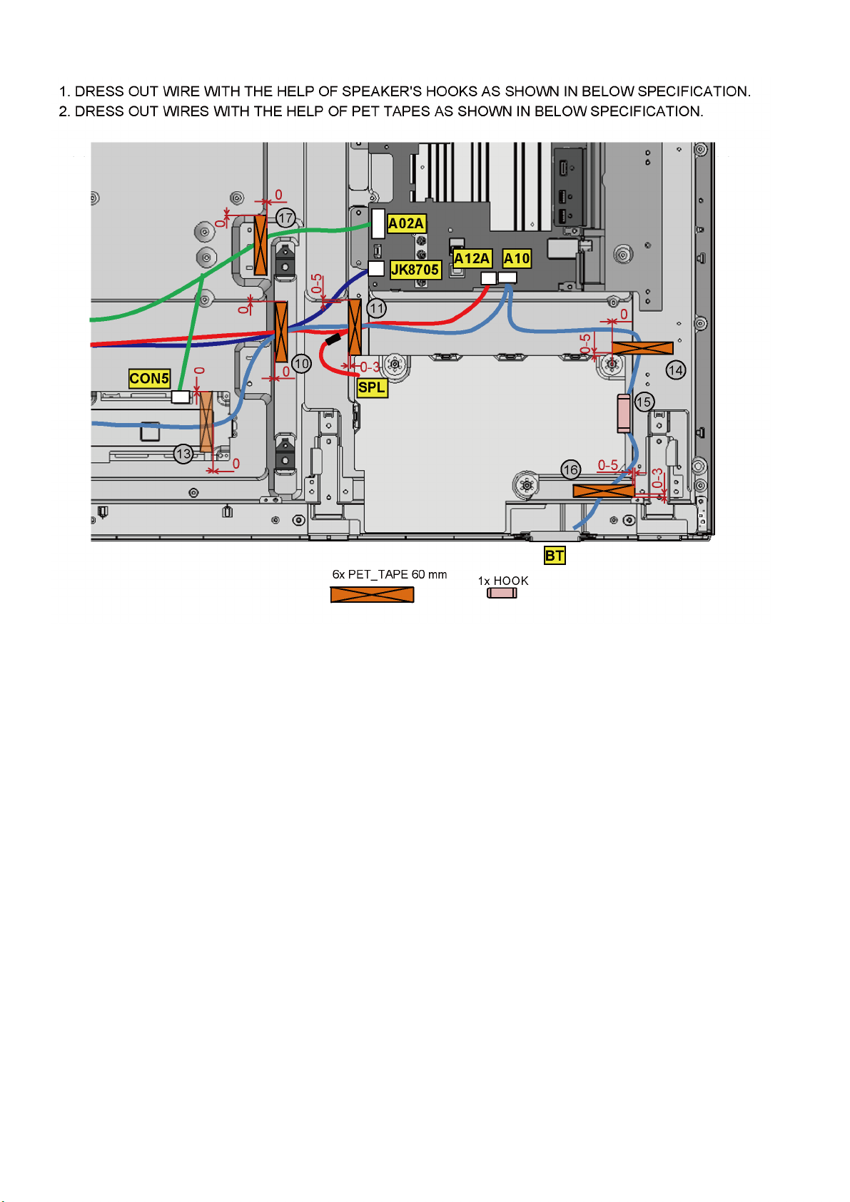
11.3. Dressing Wire --------------------------------------------- 50
12 Schematic Diagram--------------------------------------------- 55
13 Printed Circuit Board ------------------------------------------ 55
14 Exploded View and Replacement Parts List -----------55
2
Page 3
1 Safety Precautions
1.1. General Guidelines
1. When conducting repairs and servicing, do not attempt to modify the equipment, its parts or its materials.
2. When wiring units (with cables, flexible cables or lead wires) are supplied as repair parts and only one wire or some of the
wires have been broken or disconnected, do not attempt to repair or re-wire the units. Replace the entire wiring unit instead.
3. When conducting repairs and servicing, do not twist the Fasten connectors but plug them straight in or unplug them straight
out.
4. When servicing, observe the original lead dress. If a short circuit is found, replace all parts which have been overheated or
damaged by the short circuit.
5. After servicing, see to it that all the protective devices such as insulation barriers, insulation papers shields are properly
installed.
6. After servicing, make the following leakage current checks to prevent the customer from being exposed to shock hazards.
1.2. Touch-Current Check
1. Plug the AC cord directly into the AC outlet. Do not use an isolation transformer for this check.
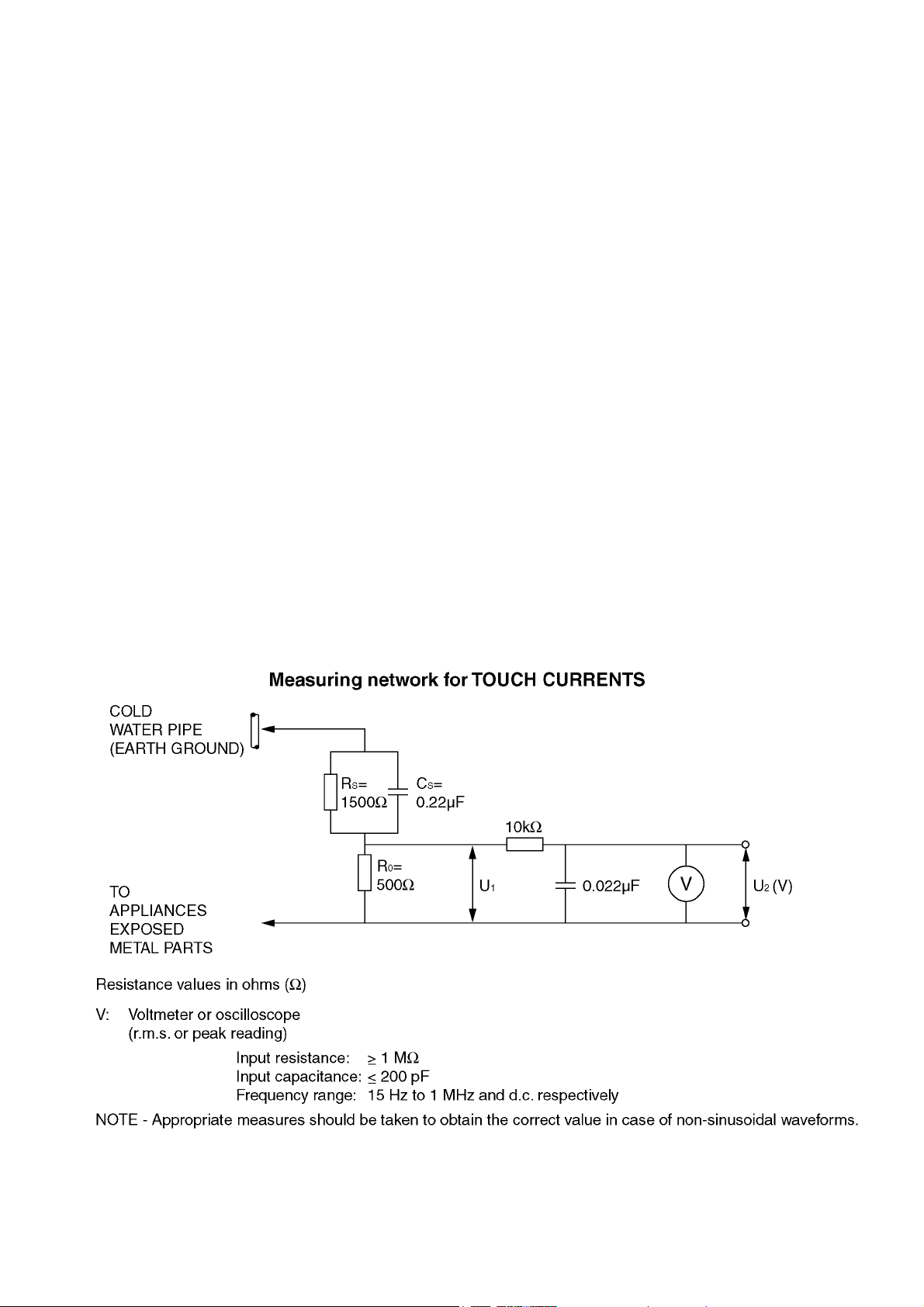
2. Connect a measuring network for touch currents between each exposed metallic part on the set and a good earth ground
such as a water pipe, as shown in Figure 1.
3. Use Leakage Current Tester (Simpson 228 or equivalent) to measure the potential across the measuring network.
4. Check each exposed metallic part, and measure the voltage at each point.
5. Reserve the AC plug in the AC outlet and repeat each of the above measure.
6. The potential at any point (TOUCH CURRENT) expressed as voltage U
For a. c.: U1 = 35 V (peak) and U2 = 0.35 V (peak);
For d. c.: U
Note:
The limit value of U
mA d. c.
The limit value U
7. In case a measurement is out of the limits specified, there is a possibility of a shock hazard, and the equipment should be
repaired and rechecked before it is returned to the customer.
= 1.0 V,
1
= 0.35 V (peak) for a. c. and U1 = 1.0 V for d. c. correspond to the values 0.7 mA (peak) a. c. and 2.0
2
= 35 V (peak) for a. c. correspond to the value 70 mA (peak) a. c. for frequencies greater than 100 kHz.
1
and U2, does not exceed the following values:
1
Figure 1
3
Page 4

2Warning
2.1. Prevention of Electrostatic Discharge (ESD) to Electrostatically Sensitive (ES) Devices
Some semiconductor (solid state) devices can be damaged easily by static electricity. Such components commonly are called
Electrostatically Sensitive (ES) Devices. Examples of typical ES devices are integrated circuits and some field-effect transistors and
semiconductor [chip] components. The following techniques should be used to help reduce the incidence of component damage
caused by electrostatic discharge (ESD).
1. Immediately before handling any semiconductor component or semiconductor-equipped assembly, drain off any ESD on your
body by touching a known earth ground. Alternatively, obtain and wear a commercially available discharging ESD wrist strap,
which should be removed for potential shock reasons prior to applying power to the unit under test.
2. After removing an electrical assembly equipped with ES devices, place the assembly on a conductive surface such as
aluminum foil, to prevent electrostatic charge buildup or exposure of the assembly.
3. Use only a grounded-tip soldering iron to solder or unsolder ES devices.
4. Use only an anti-static solder removal device. Some solder removal devices not classified as [anti-static (ESD protected)] can
generate electrical charge sufficient to damage ES devices.
5. Do not use freon-propelled chemicals. These can generate electrical charges sufficient to damage ES devices.
6. Do not remove a replacement ES device from its protective package until immediately before you are ready to install it. (Most
replacement ES devices are packaged with leads electrically shorted together by conductive foam, aluminum foil or
comparable conductive material).
7. Immediately before removing the protective material from the leads of a replacement ES device, touch the protective material
to the chassis or circuit assembly into which the device will be installed.
Caution
Be sure no power is applied to the chassis or circuit, and observe all other safety precautions.
8. Minimize bodily motions when handling unpackaged replacement ES devices. (Otherwise ham less motion such as the
brushing together of your clothes fabric or the lifting of your foot from a carpeted floor can generate static electricity (ESD)
sufficient to damage an ES device).
4
Page 5
2.2. About lead free solder (PbF)
Note: Lead is listed as (Pb) in the periodic table of elements.
In the information below, Pb will refer to Lead solder, and PbF will refer to Lead Free Solder.
The Lead Free Solder used in our manufacturing process and discussed below is (Sn+Ag+Cu).
That is Tin (Sn), Silver (Ag) and Copper (Cu) although other types are available.
This model uses Pb Free solder in it's manufacture due to environmental conservation issues. For service and repair work, we'd
suggest the use of Pb free solder as well, although Pb solder may be used.
PCBs manufactured using lead free solder will have the PbF within a leaf Symbol PbF stamped on the back of PCB.
Caution
• Pb free solder has a higher melting point than standard solder. Typically the melting point is 50 ~ 70 °F (30~40 °C) higher. Please
use a high temperature soldering iron and set it to 700 ± 20 °F (370 ± 10 °C).
• Pb free solder will tend to splash when heated too high (about 1100 °F or 600 °C).
If you must use Pb solder, please completely remove all of the Pb free solder on the pins or solder area before applying Pb
solder. If this is not practical, be sure to heat the Pb free solder until it melts, before applying Pb solder.
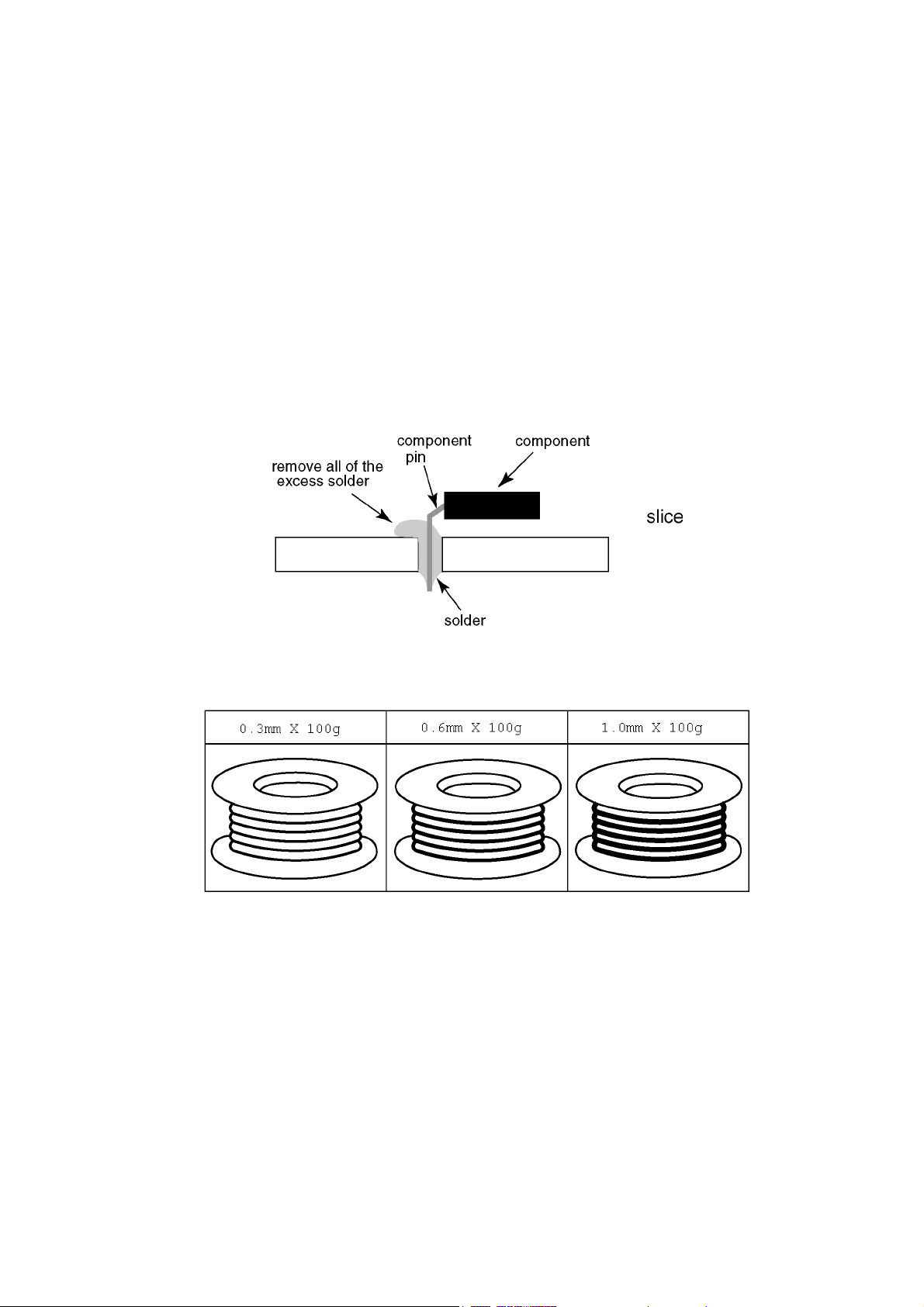
• After applying PbF solder to double layered boards, please check the component side for excess solder which may flow onto the
opposite side. (see figure below)
Suggested Pb free solder
There are several kinds of Pb free solder available for purchase. This product uses Sn+Ag+Cu (tin, silver, copper) solder.
However, Sn+Cu (tin, copper), Sn+Zn+Bi (tin, zinc, bismuth) solder can also be used.
5
Page 6
3 Service Navigation
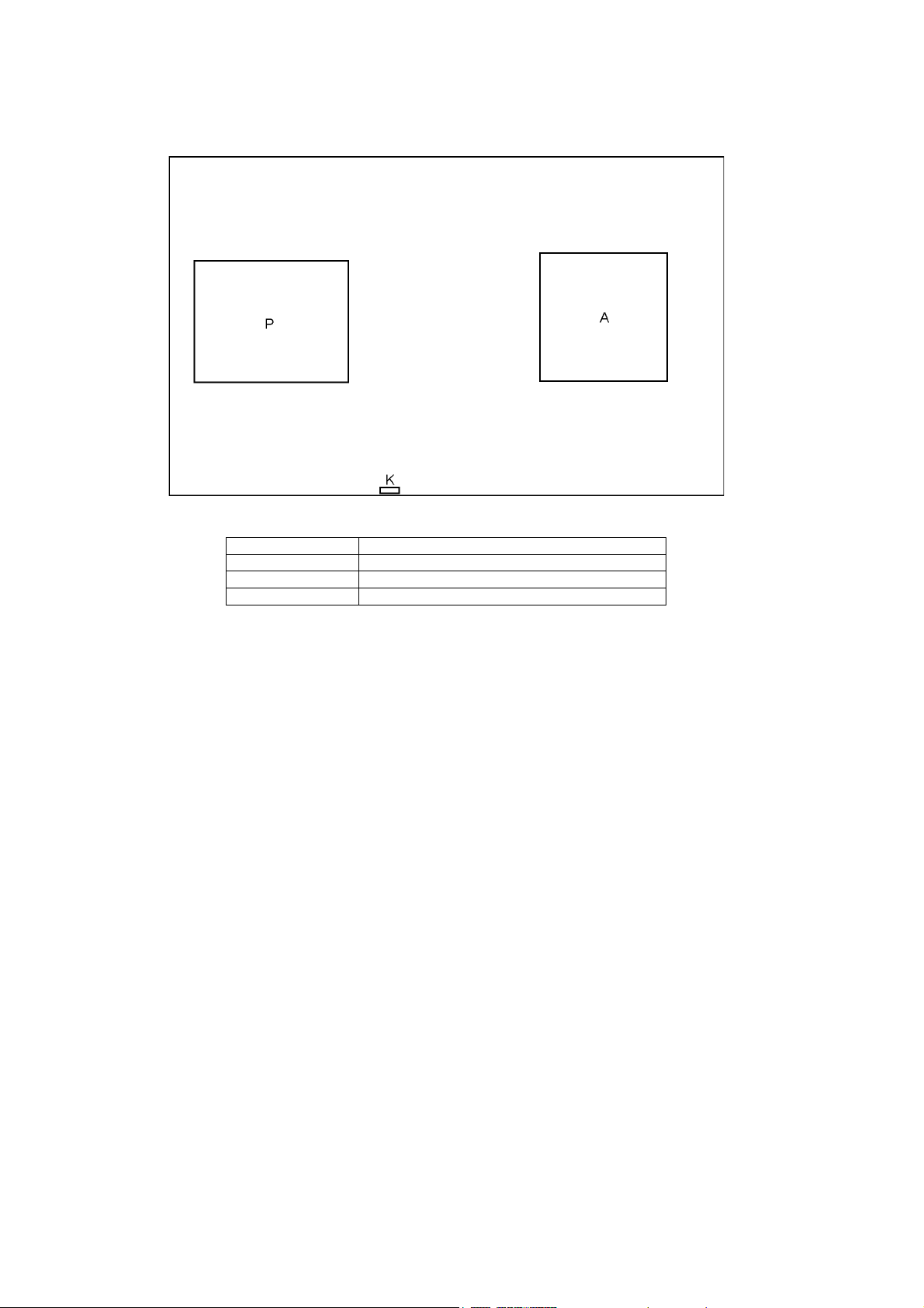
3.1. PCB Layout
Board Name Function
A-Board Main
P-Board Power Supply / Switch / LED Driver
K-Board IR/LED/CATS
6
Page 7

4 Specifications
Product fiche
Energy efficiency class A
Visible screen size (diagonal) 146 cm / 58 inches
On mode average power consumption 113 W
Annual energy consumption
Standby power consumption
Off mode power consumption 0.30 W
Screen resolution 3 840 (W) 2 160 (H)
*1: Energy consumption XYZ kWh per year, based on the power consumption of the television operating 4 hours per day for 365 days.
The actual energy consumption will depend on how the television is used.
*2: when the TV is turned off with the remote control and no function is active.
For the information of rated power consumption, refer to the label on the TV back cover.
TV
Dimensions (W × H × D)
(DX750B/F)
(Style1 / Style2) 1 290 mm 813 mm 376 mm (With Pedestal)
(Style3 / Style4) 1 336 mm 798 mm 376 mm (With Pedestal)
(DX750E)
(Style1) 1 290 mm 805 mm 234 mm (With Pedestal)
(Style2) 1 290 mm 820 mm 234 mm (With Pedestal)
Mass
(DX750B/F)
(DX750E)
Power source AC 220-240 V, 50 / 60 Hz
Panel LED LCD panel
Sound
Speaker output 20 W (10 W + 10 W)
Headphones M3 (3.5 mm) stereo mini Jack 1
Connection terminals
AV input (COMPONENT / VIDEO)
VIDEO RCA PIN Type 1 1.0 V [p-p] (75 )
AUDIO L - R RCA PIN Type 2 0.5 V [rms]
Y 1.0 V [p-p] (including synchronisation)
, PR/C
P
B/CB
HDMI 1 / 2 / 3 / 4 input TYPE A Connectors
Card slot Common Interface slot (complies with CI Plus) 1
ETHERNET RJ45, IEEE802.3 10BASE-T / 100BASE-TX
USB 1 / 2 / 3
USB1: DC 5 V, Max. 900 mA [SuperSpeed USB (USB 3.0)]
USB2 / 3: DC 5 V, Max. 500 mA [Hi-Speed USB (USB 2.0)]
DIGITAL AUDIO output PCM / Dolby Digital / DTS, Fibre optic
*1
*2
R
156 kWh
0.50 W
1 290 mm 753 mm 41 mm (TV only)
1 290 mm 753 mm 41 mm (TV only)
1 290 mm 753 mm 41 mm (TV only)
1 290 mm 753 mm 41 mm (TV only)
24.5 kg Net (With Pedestal)
23.0 kg Net (TV only)
24.0 kg Net (With Pedestal)
23.0 kg Net (TV only)
± 0.35 V [p-p]
HDMI 1 : 4K/60p, 3D (3D content of 4K format is not supported), Content Type, Deep
Colour, x.v.Colour™
HDMI 2 : 4K/60p, 3D (3D content of 4K format is not supported), Content Type, Audio
Return Channel, Deep Colour, x.v.Colour™
HDMI 3/4 : 4K/30p, 3D (3D content of 4K format is not supported), Content Type, Deep
Colour, x.v.Colour™
• This TV supports [HDAVI control 5] function.
7
Page 8

Receiving systems / Band name (DX750B)
DVB-T / T2 Digital terrestrial services
(UK)
PAL I UHF E21 - 68
(Ireland)
PAL I VHF A - J
CATV S1 - S20
UHF E21 - E69
CATV S21 - S41 (Hyperband)
PAL 525/60 Playback of NTSC tape from some PAL Video recorders (VCR) or NTSC disc playback from
DVD player and recorder
M.NTSC Playback from M.NTSC Video recorders (VCR)
NTSC (AV input only) Playback from NTSC Video recorders (VCR)
Receiving systems / Band name (DX750E/F)
DVB-C Digital cable services (MPEG2, MPEG4-AVC(H.264) and MPEG HEVC(H.265))
DVB-T / T2 Digital terrestrial services (MPEG2, MPEG4-AVC(H.264) and MPEG HEVC(H.265))
PAL B, G, H, I, SECAM B, G, SECAM L, L’
VHF E2 - E12
CATV (S01 - S05)
VHF H1 - H2 (ITALY)
CATV S1 - S10 (M1 - M10)
PAL D, K, SECAM D, K VHF R1 - R2
VHF R6 - R12
VHF A - H (ITALY)
CATV S11 - S20 (U1 - U10)
UHF E21 - E69
CATV S21 - S41 (Hyperband)
VHF R3 - R5
UHF E21 - E69
PAL 525/60 Playback of NTSC tape from some PAL Video recorders (VCR)
M.NTSC Playback from M.NTSC Video recorders (VCR)
NTSC (AV input only) Playback from NTSC Video recorders (VCR)
Aerial input
(DX750B-UK) UHF
(DX750B-Ireland, DX750E, DX750F) VHF / UHF
Operating conditions
Temperature 0 °C - 35 °C
Humidity 20 % - 80 % RH (non-condensing)
Built-in wireless LAN
Standard compliance and Frequency range*
1
IEEE802.11a/n 5.180 GHz - 5.320 GHz, 5.500 GHz - 5.580 GHz, 5.660 GHz - 5.700 GHz
IEEE802.11b/g/n 2.412 GHz - 2.472 GHz
Security WPA2-PSK (TKIP/AES), WPA-PSK (TKIP/AES), WEP (64 bit/128 bit)
Bluetooth wireless technology*
2
Standard Compliance Bluetooth 3.0
Frequency Range 2.402 GHz - 2.480 GHz
1
*
: The frequency and channel differ depending on the country.
2
: Not all the Bluetooth compatible devices are available with this TV. Up to 5 devices can be used simultaneously (except the 3D Eyewear).
*
Note
• Design and Specifications are subject to change without notice. Mass and Dimensions shown are approximate.
• For information about the power consumption, display resolution, etc., refer to Product fiche.
• For information about the open source software, refer to [eHELP] (Support > Licence).
8
Page 9
5 Technical Descriptions
5.1. Specification of KEY for CI PLUS, DTCP-IP, HDCP2.2, NETFLIX, WIDEVINE, ONE-TO-ONE, DIMORA, FREETIME and HDCP1.4
5.1.1. General information:
1. eMMC (IC8920) for spare parts has the seed of KEY for each.
2. The final KEY data will be generated by Main IC (IC8000) when SELF CHECK was done and are stored in both Main IC
(IC8000) and eMMC (IC8920).
All KEY are not generated for all models.
The necessary KEY are only generated and stored depend on the feature of models.
5.1.2. Replacement of ICs:
When Main IC (IC8000) is replaced, eMMC (IC8920) should be also replaced with new one the same time.
When eMMC (IC8920) is replaced, Main IC (IC8000) is not necessary to be replaced the same time.
After the replacement of IC, SELF CHECK should be done to generate the final KEY data.
Note:
Keys HDCP1.4 (SINK) for MTK HDMI and HDCP2.2 (SINK) for MTK HDMI are not displayed in SELF CHECK.
Connect the 4K60Hz with HDCP2.2 compatible equipment to HDMI1/2 for verification of key [HDCP2.2 (SINK) for MTK HDMI].
Connect the 4K30Hz compatible equipment to HDMI1/2/3/4 for verification of key [HDCP1.4 (SINK) for MTK HDMI].
How to SELF CHECK: While pressing [VOLUME ( - )] button on the main unit, press [MENU] button on the remote control for more
than 3 seconds.
TV will be forced to the factory shipment setting after this SELF CHECK.
5.1.3. Model and Keys:
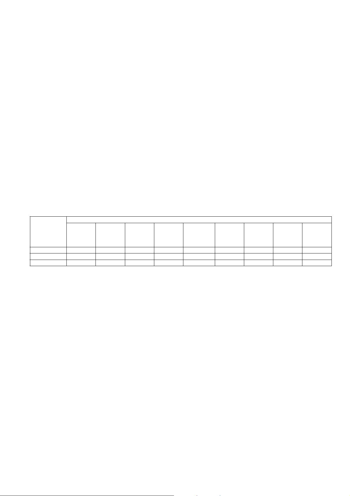
Model No. Keys
CI PLUS DTCP-IP HDCP2.2
(SINK)
for MTK
TX-58DX750B Yes Yes Yes Yes Yes Yes Yes Yes Yes
TX-58DX750E Yes Yes Yes Yes Yes Yes None Yes Yes
TX-58DX750F Yes Yes Yes Yes Yes Yes None Yes Yes
NETFLIX
WIDEVINE
ONE-TO-ONE
(For USB
Rec.)
DIMORA FREETIME HDCP1.4
(SINK)
for MTK
HDMI
HDCP2.2
(SINK)
for MTK
HDMI
5.2. USB HDD Recording
5.2.1. General information:
Digital TV programmes can be recorded in USB HDD.
A One-to-One key generated in A-board by SELF CHECK binds TV and USB-HDD for communication.
That key is only one key for them. If the key is difference, TV can not access USB-HDD.
Caution:
New key will be generated by following SELF CHECK and previous TV programmes recorded in USB HDD will not be
viewed.
SELF CHECK: While pressing [VOLUME ( - )] button on the main unit, press [MENU] button on the remote control for
more than 3 seconds.
9
Page 10
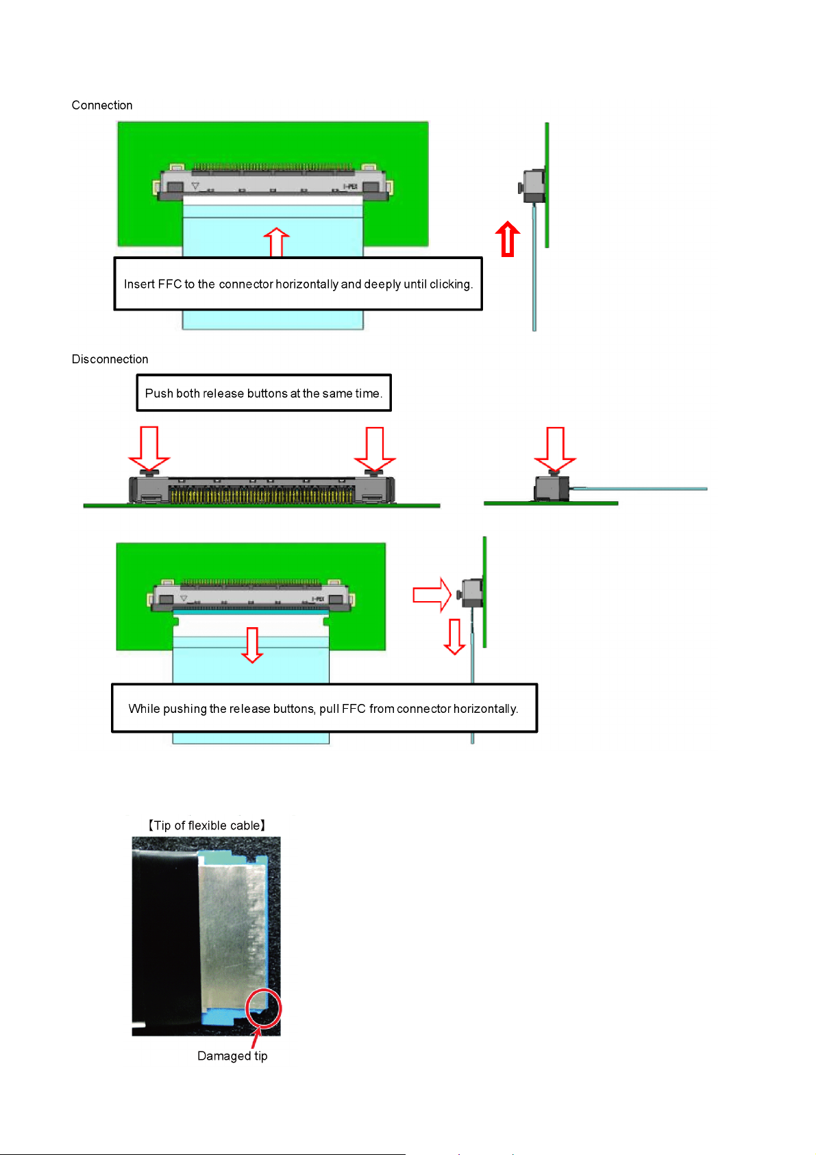
5.3. How to connect and disconnect for A15 and A16 connectors on A board
If the flexible cable is inserted at a slant, the tip of the cable may be damaged.
In this case, the flexible cable should be replaced because a damaged tip causes connection failure, resulting in image defect.
10
Page 11
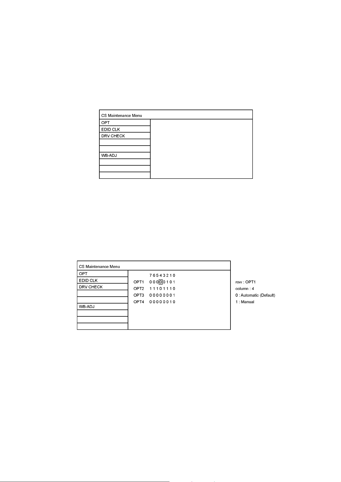
6 CS Maintenance Menu
6.1. How to enter into CS Maintenance Menu
6.1.1. Purpose
After exchange parts, check and adjust the contents of adjustment mode.
While pressing [VOLUME ( - )] button of the main unit, press [ RED ] button of the remote control three times within 2 seconds.
Note:
CS Maintenance Menu can not be entered when 3D signal input.
Input 2D signal to enter CS Maintenance Menu.
6.1.2. Key command
Press the Cursor key [Up/Down] on the remote control to select the functions.
6.1.3. How to exit
Press the [EXIT] button on the remote control.
6.2. Repack
1. Select [OPT] in CS Maintenance Menu.
2. Press [OK] button or Cursor key [Right] on the remote control.
Exit:
Press the [Exit] button or the [Return] button on the remote control.
11
Page 12
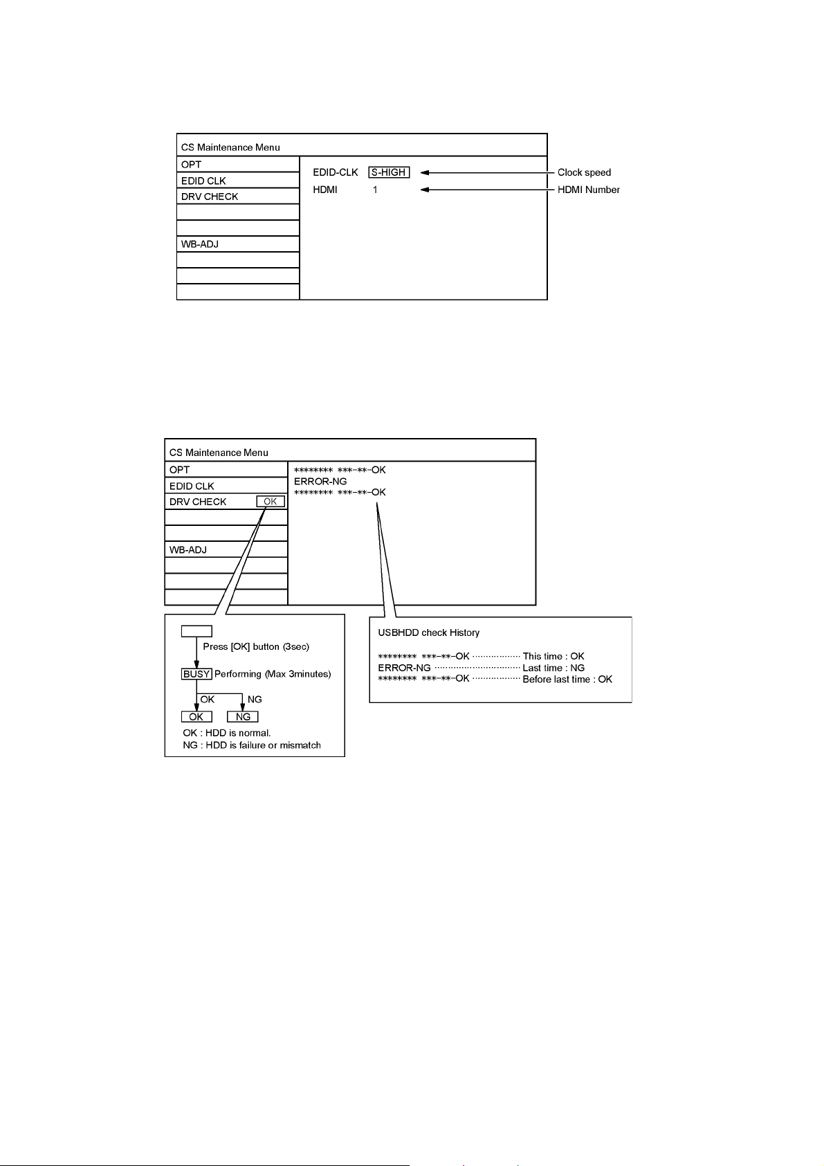
6.3. EDID Clock
1. Select [EDID CLK] in CS Maintenance Menu.
2. Press [OK] button or Cursor key [Right] on the remote control.
Exit:
Press the [Exit] button or the [Return] button on the remote control.
6.4. USB HDD Drive Check
1. Select [DRV CHECK] in CS Maintenance Menu.
2. Press [OK] button or Cursor key [Right] on the remote control.
Exit:
Press the [Return] button on the remote control.
12
Page 13
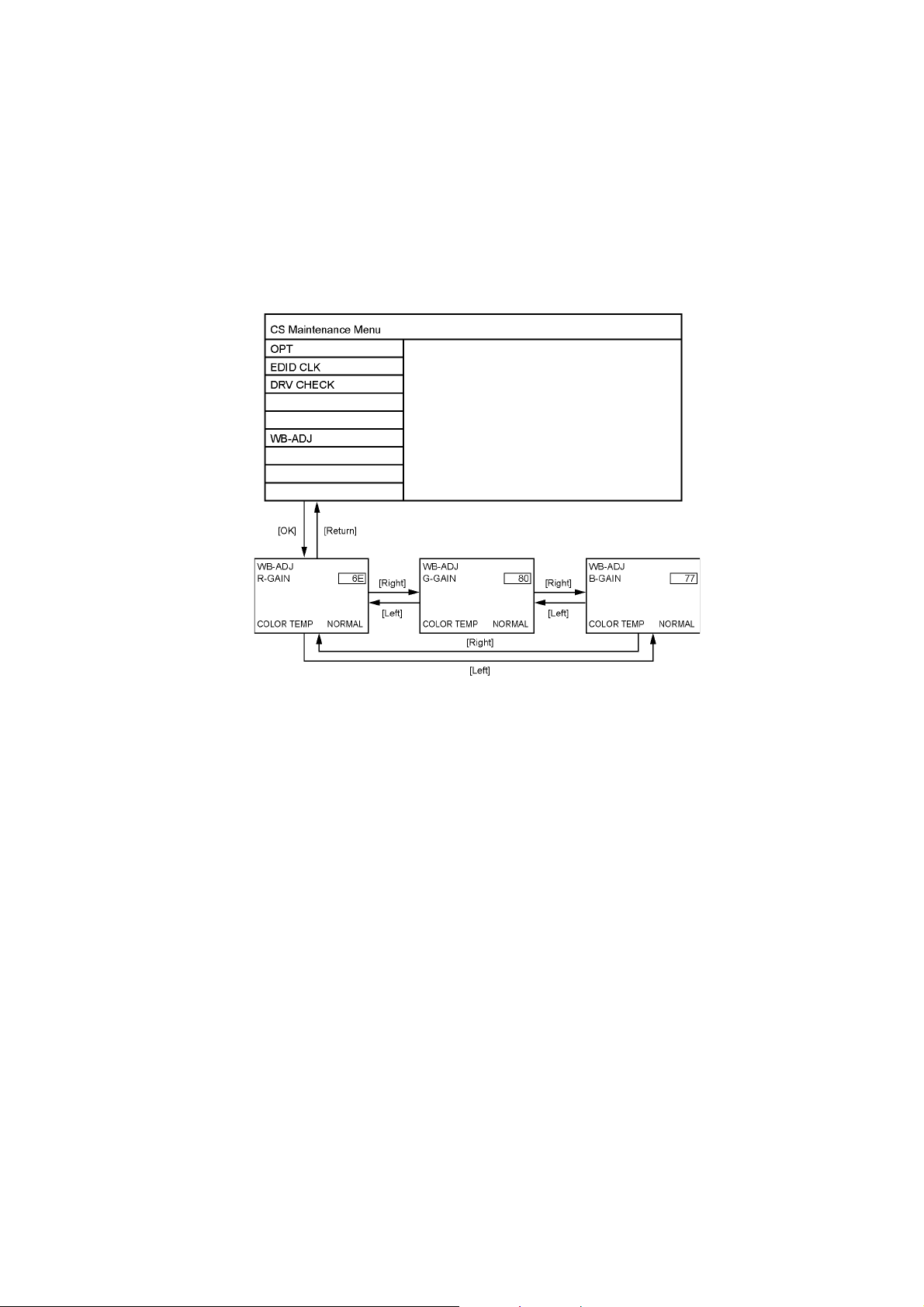
6.5. White Balance Adjustment
After LCD PANEL or A-Board is replaced and repaired, perform [White balance adjustment] in case of necessity for test / check
([White balance adjustment] is not required basically).
1. Select [W/B ADJ] in CS Maintenance Menu.
2. Press [OK] button on the remote control.
Note for performing [White balance adjustment]
Make a note for the setting values before changing if the settings of [R-GAIN], [B-GAIN] and [G-GAIN] in [WB-ADJ] will be
changed.
3. Press the cursor key [Up/Down] on the remote control to change the data value, and press [OK] button on the remote control
to store the value for this model.
• COLOR TEMP : Press the [Option] button of the remote control to change the color temperature. (COOL/NORMAL/WARM/
TUNNIG)
Exit:
Press the [Return] button on the remote control.
13
Page 14
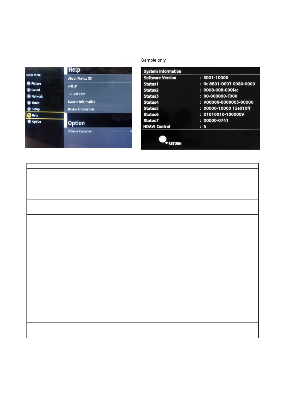
6.6. System Information
6.6.1. How to access
1. While pressing [MENU] button on the remote control.
2. To select [? Help] and then to select [System Information].
System Information
SW version 3001-10000-abcde 3001
10000
abcde
Status1 0c 8801-0003 0080-0000 0c
8801-0003
0080-0000
Status2 0008-008-000fac 0008
008
000fac
Status3 00-000000-F000 00
00
00
00
F000
Status4 A00000-0000003-00000 A
00000
0000003
00000
Status5 00000-10000 15e010ff 0
0
0
0
0
1
0000
15e010ff
Status6 01010010-1000009 01010010
1000009
Status7 00000-0741 00000
0741
HDAVI Control 5 VIERA Link version is displayed
Peaks SW
GenX Main
GenX Sub (optinal)
Outer model ID
Inner model ID
Panel inch size
LSI Package
LSI Release
Model data version
Number of bad block in NAND Flash (dec)
Peaks reboot counter
System crash counter
Emergency (SOS) counter
Peaks NAND Maker ID
Power-On period (A <= 100hrs, B <= 200hrs, C > 200hrs)
Total Power-On time (dec, max is 65535)
Power-On timer (dec, max is 1048575)
Fixed (always)
SOS history (latest)
SOS history (last time)
SOS history (last but one)
SOS history (2
SOS history (1
Self-check _0-never selfcheck
1-production selfcheck by "FF" or USCM
2-user selfcheck by pressing "OK"
Fixed (always)
Panel ID
Peaks EEPROM version
STM EEPROM version
STM ROMCOR version
AJAX_CE version
nd
time after shipping)
st
time after shipping)
6.6.2. How to exit
Press the [RETURN] button on the remote control.
14
Page 15

6.7. Hotel mode
6.7.1. Purpose
Restrict a function for hotels.
6.7.2. Access command to the Hotel mode setup menu
In order to display the Hotel mode setup menu,
please enter the following command (within 2 seconds).
[TV]: Vol.[Down] + [REMOTE] : AV (3 times)
Then, the Hotel mode setup menu is displayed.
6.7.3. To exit the Hotel mode setup menu
Switch off the power with the [POWER] button on the main unit
or the [POWER] button on the remote control.
6.7.4. Explain the Hotel mode setup menu
Item Function
Hotel Mode Select hotel mode On/Off
Initial INPUT Select input signal modes.
Set the input, when each time power is switched
on.
Selection :
Off, Analogue, DVB (B), DVB-C (E/F),
DVB-T (E/F), AV, HDMI1, HDMI2, HDMI3, HDMI4
• Off: give priority to a last memory.
Initial POS Select programme number.
Selection :
Off/0 to 99
• Off: give priority to a last memory
Initial VOL Level Adjust the volume when each time power is
switched on.
Selection/Range :
Off/0 to 100
• Off: give priority to a last memory
Maximum VOL
Level
Button Lock Select local key conditions.
Remote Lock Select remote control key conditions.
Private Information Select private information for VIERA Cast is Keep
Adjust maximum volume.
Range :
0 to 100
Selection :
Off/SETUP/MENU
• Off: altogether valid
• SETUP: only F-key is invalid
(Tuning guide (menu) can not be selected.)
• MENU: only F-key is invalid
(only Volume/Mute can be selected.)
Selection :
Off/SETUP/MENU/VOD
• Off: altogether valid
• SETUP: only Setup menu is invalid
• MENU: Picture/Sound/Setup menu are invalid
• VOD: NETFLIX service is invalid
or Reset if Hotel mode is set to [On] when TV
power on.
Selection :
Keep/Reset
• Keep: private information for VIERA Cast is
keep
• Reset: private information for VIERA Cast is
reset
15
Page 16
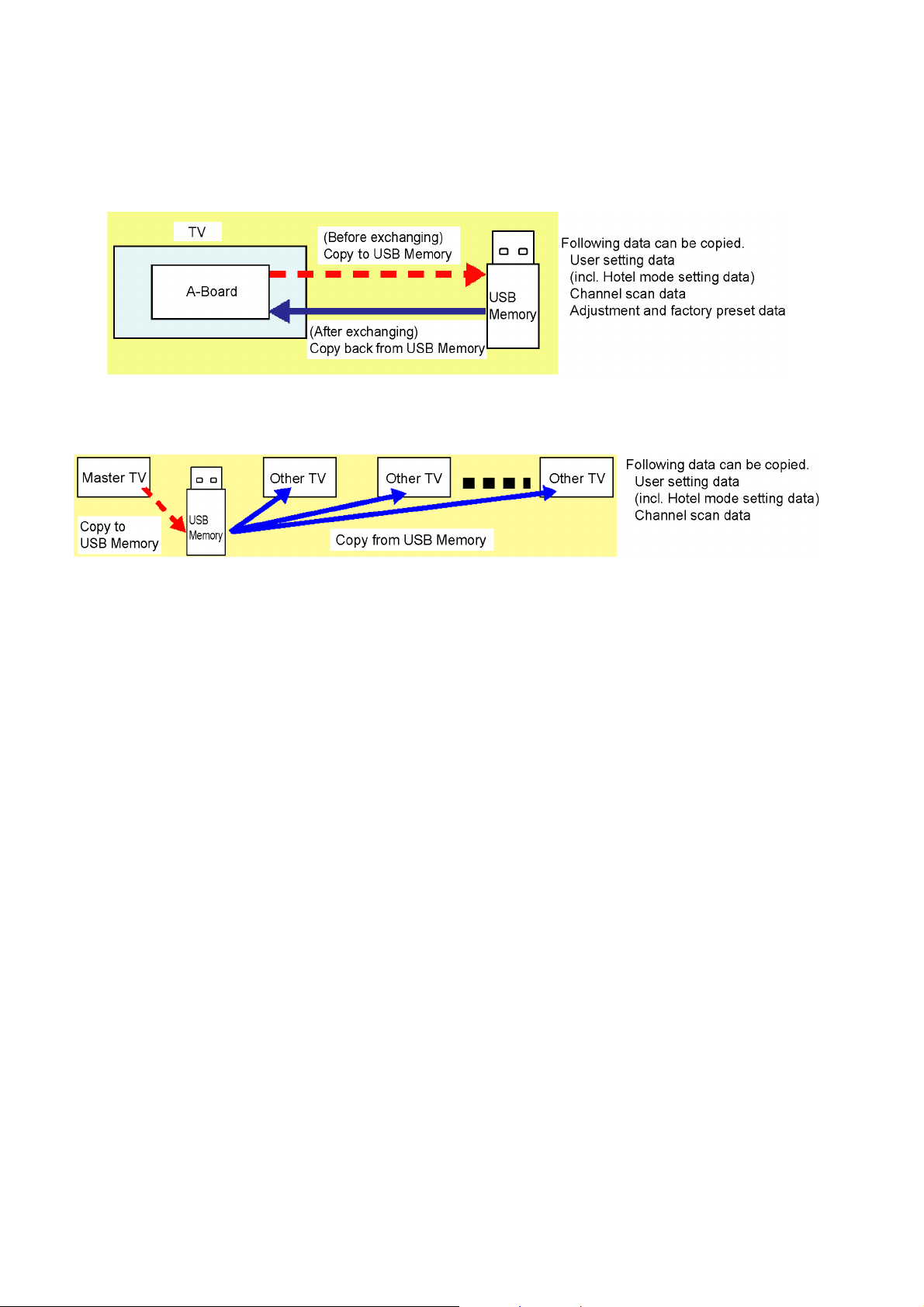
6.8. Data Copy by USB Memory
Note:
SD card can not be used for Data Copy.
6.8.1. Purpose
(a) Board replacement (Copy the data when exchanging A-board):
When exchanging A-board, the data in original A-board can be copied to USB Memory and then copy to new A-board.
(b) Hotel (Copy the data when installing a number of units in hotel or any facility):
When installing a number of units in hotel or any facility, the data in master TV can be copied to USB Memory and then copy to
other TVs.
6.8.2. Preparation
Make pwd file as startup file for (a) or (b) in a empty USB Memory.
1. Insert a empty USB Memory to your PC.
2. Right-click a blank area in a USB Memory window, point to New, and then click text document. A new file is created by default
(New Text Document.txt).
3. Right-click the new text document that you just created and select rename, and then change the name and extension of the
file to the following file name for (a) or (b) and press ENTER.
File name:
(a) For Board replacement : boardreplace.pwd
(b) For Hotel : hotel.pwd
Note:
Please make only one file to prevent the operation error.
No any other file should not be in USB Memory.
16
Page 17
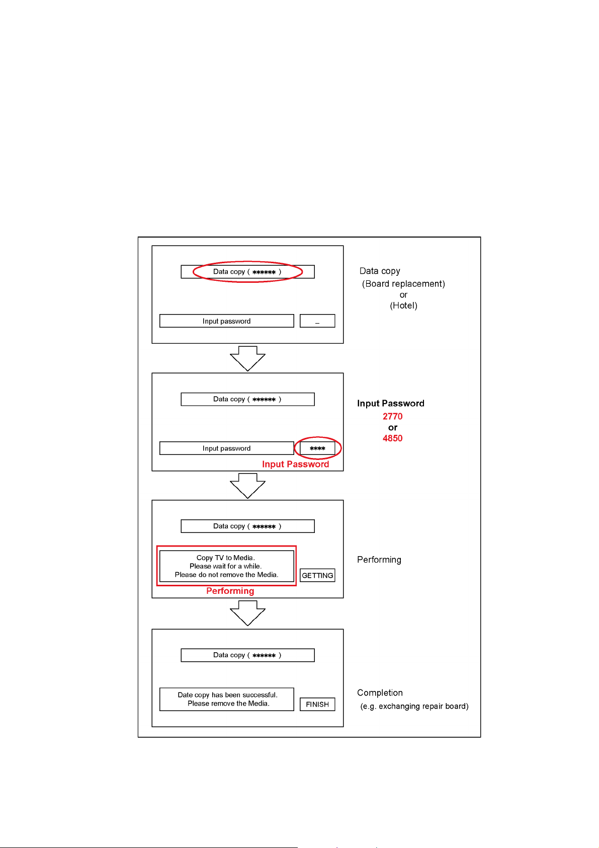
6.8.3. Data copy from TV set to USB Memory
1. Turn on the TV set.
2. Insert USB Memory with a startup file (pwd file) to USB terminal.
On-screen Display will be appeared according to the startup file automatically.
3. Input a following password for (a) or (b) by using remote control.
(a) For Board replacement : 2770
(b) For Hotel : 4850
Data will be copied from TV set to USB Memory.
It takes around 2 to 6 minutes maximum for copying.
4. After the completion of copying to USB Memory, remove USB Memory from TV set.
5. Turn off the TV set.
Note:
Following new folder will be created in USB Memory for data from TV set.
(a) For Board replacement : user_setup
(b) For Hotel : hotel
17
Page 18
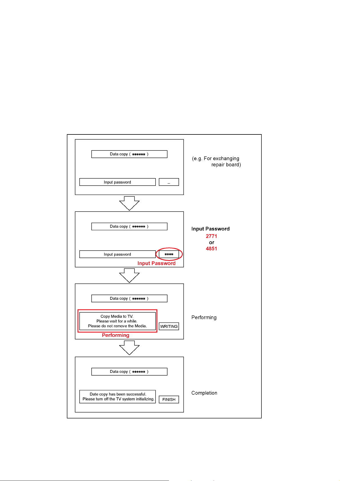
6.8.4. Data copy from USB Memory to TV set
1. Turn on the TV set.
2. Insert USB Memory with Data to USB terminal.
On-screen Display will be appeared according to the Data folder automatically.
3. Input a following password for (a) or (b) by using remote control.
(a) For Board replacement : 2771
(b) For Hotel : 4851
Data will be copied from USB Memory to TV set.
4. After the completion of copying to USB Memory, remove USB Memory from TV set.
(a) For Board replacement : Data will be deleted after copying (Limited one copy).
(b) For Hotel : Data will not be deleted and can be used for other TVs.
5. Turn off the TV set.
Note:
1. Depending on the failure of boards, function of Data copy for board replacement does not work.
2. This function can be effective among the same model numbers.
18
Page 19
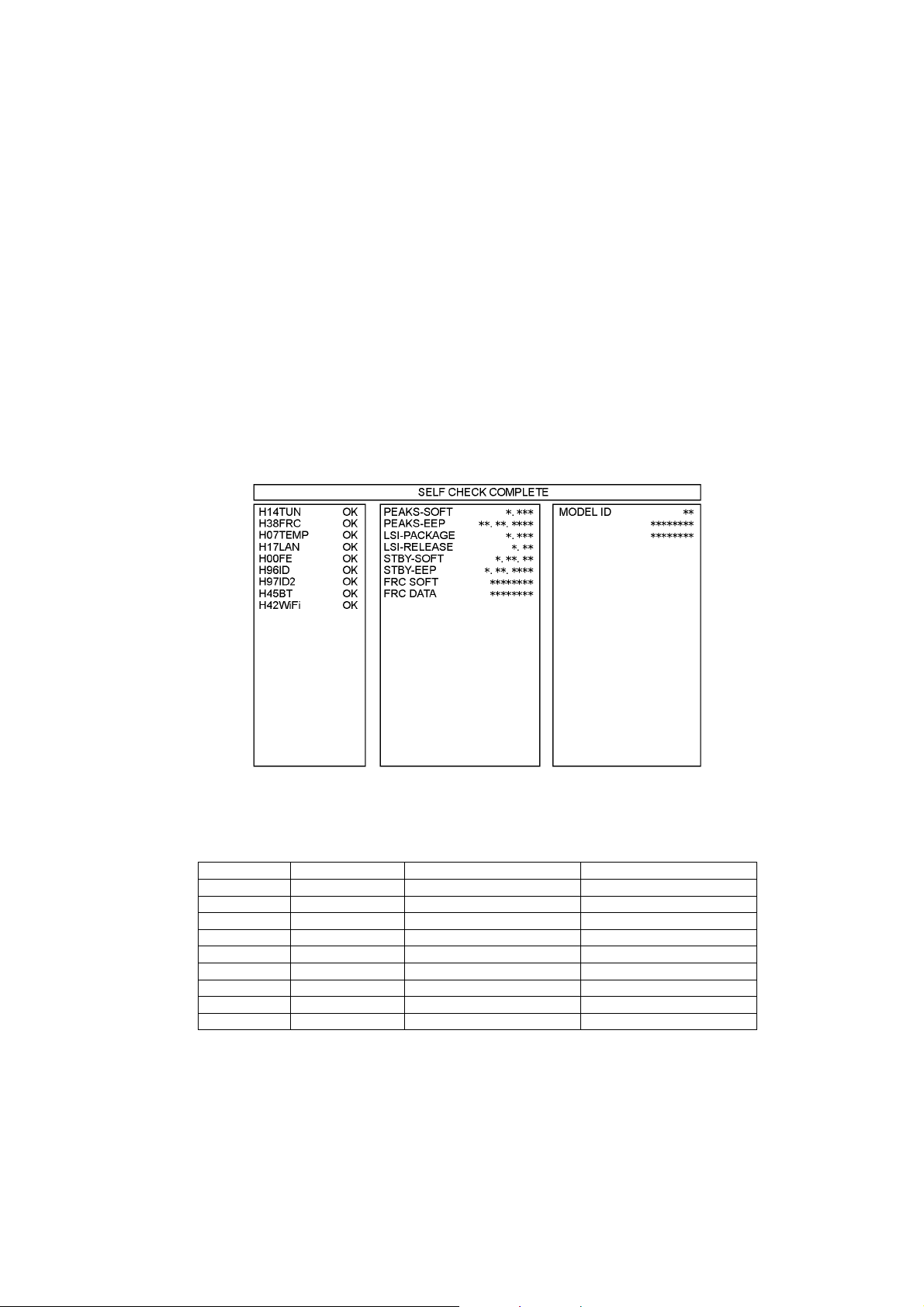
7 Troubleshooting Guide
Use the self-check function to test the unit.
1. Checking the IIC bus lines
2. Power LED Blinking timing
7.1. Check of the IIC bus lines
7.1.1. How to access
7.1.1.1. Self-check indication only:
Produce TV reception screen, and while pressing [VOLUME ( - )] button on the main unit, press [BLUE] button on the remote
control for more than 3 seconds.
7.1.1.2. Self-check indication and forced to factory shipment setting:
Caution:
New key will be generated and previous TV programmes recorded in USB HDD will not be viewed. (See USB HDD
Recording)
Produce TV reception screen, and while pressing [VOLUME ( - )] button on the main unit, press [MENU] button on the remote
control for more than 3 seconds.
7.1.2. Screen display
7.1.3. Check Point
Confirm the following parts if NG was displayed.
DISPLAY Check Ref. No. Description Check Point
H14TUN IC6950 TUNER A-BOARD
H38FRC IC9000 FRC A-BOARD
H07TEMP IC5911 TEMP SENSOR A-BOARD
H17LAN ETHERNET A-BOARD / LAN
H00FE IC6800 DEMODULATOR A-BOARD
H96ID ID A-BOARD
H97ID2 ID2 A-BOARD
H45BT BLUETOOTH A-BOARD / BLUETOOTH
H42WiFi WiFi A-BOARD / WiFi
7.1.4. Exit
Disconnect the AC cord from wall outlet or press the [POWER] button on the main unit for 3 seconds to turn off and then turn on
automatically.
19
Page 20

7.2. Power LED Blinking timing chart
1. Subject
Information of LED Flashing timing chart.
2. Contents
When an abnormality has occurred the unit, the protection circuit operates and reset to the stand by mode. At this time, the
defective block can be identified by the number of blinks of the Power LED on the front panel of the unit.
Blinking Times Contents Check point
1 BL SOS LCD PANEL
P-Board
7 SUB 3.3V / 1.0V P-Board
9 SOUND SOS A-Board
10 FRC / NVT SOS A-Board
13 EMERGENCY SOS A-Board
A-Board
Speaker
7.3. LCD Panel test mode
Purpose:
To find the possible failure point where in LCD Panel or Printed Circuit Board when the abnormal picture is displayed.
How to Enter:
While pressing [VOLUME ( - )] button of the main unit, press [YELLOW] button of the remote control three times within 2
seconds.
How to Exit:
Switch off the power with the [POWER] button on the main unit or the [POWER] button on the remote control.
How to confirm:
If the abnormal picture is displayed, go into LCD Panel test mode to display the several test patterns.
And then, judge by the following method.
Still abnormal picture is displayed: The cause must be in LCD Panel.
Normal picture is displayed: The cause must be in A board.
Remarks:
The test pattern is created by the circuit in LCD Panel.
In LCD Panel test mode, this test pattern is displayed unaffected by signal processing for RF or input signal.
If the normal picture is displayed, LCD Panel must be okay and the cause of failure must be in A board.
20
Page 21
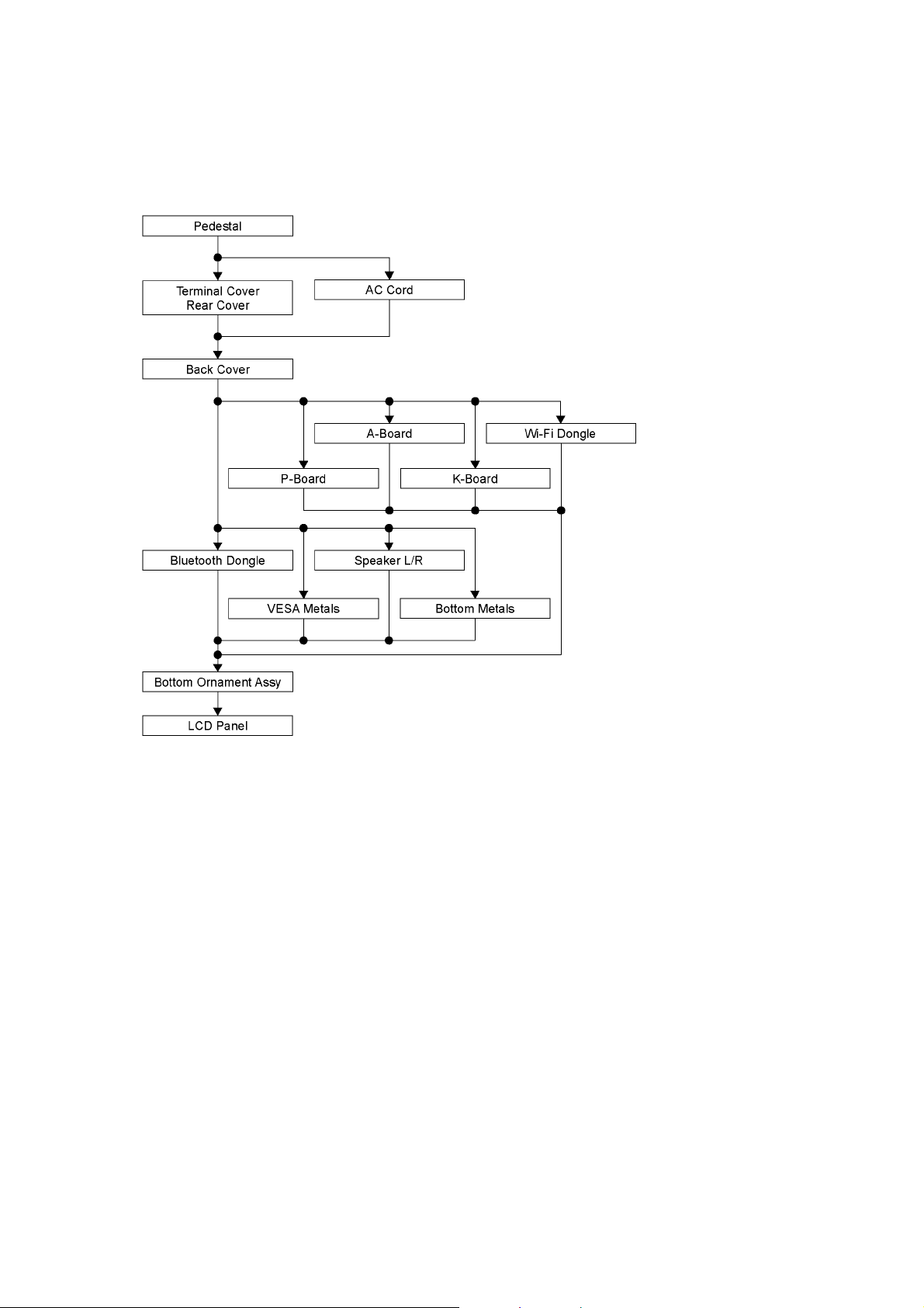
8 Disassembly and Assembly Instructions
8.1. Disassembly Flow Chart for the Unit
This is a disassembly chart.
When assembling, perform this chart conversely.
21
Page 22
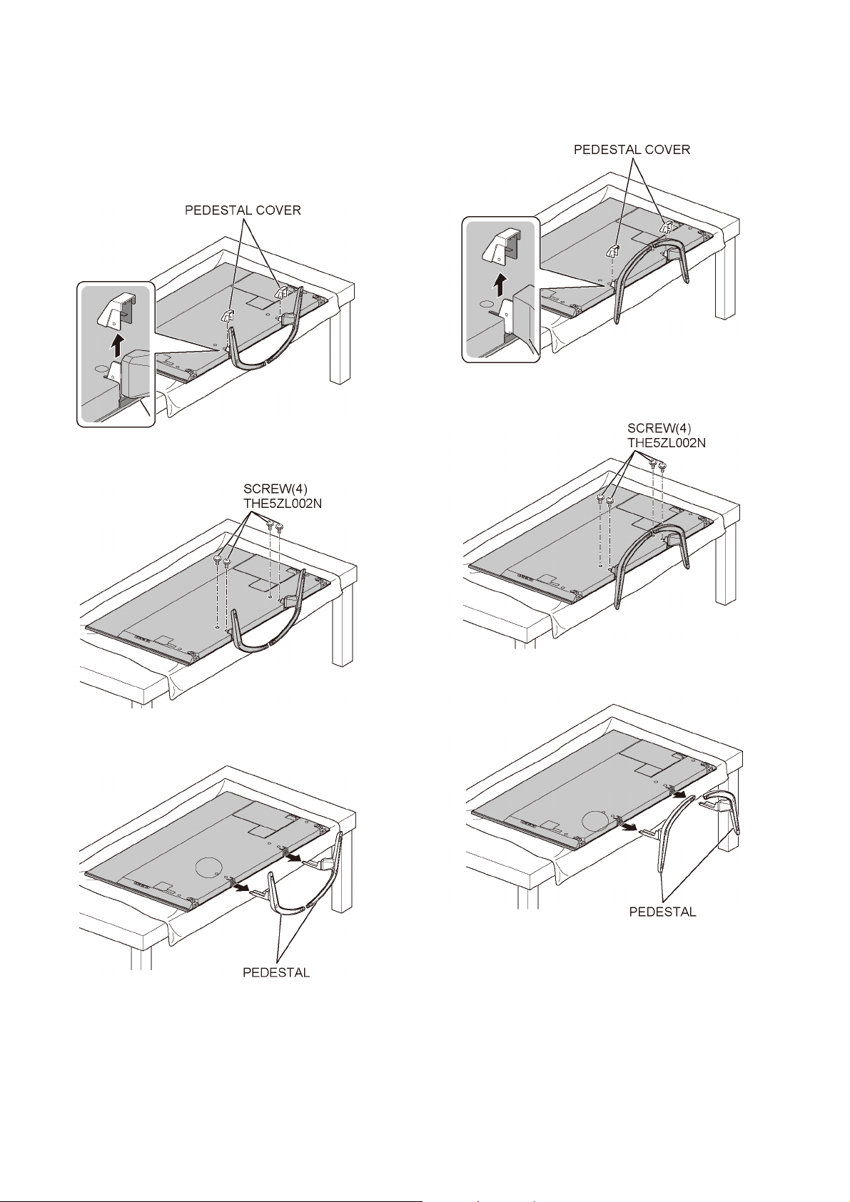
8.2. Disassembly Procedure for the Unit
Lay down the unit so that the rear cover faces upward.
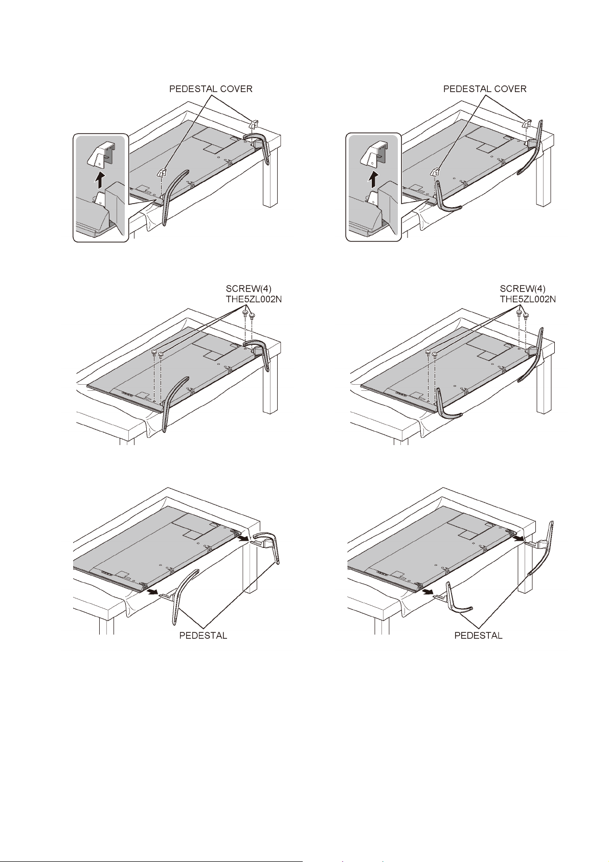
8.2.1. Pedestal
[DX750B/F]
[Style1]
1. Remove the 2 Pedestal Covers.
2. Remove the 4 screws.
[Style2]
1. Remove the 2 Pedestal Covers.
2. Remove the 4 screws.
3. Remove the Pedestal L/R.
3. Remove the Pedestal L/R.
22
Page 23
[Style3]
1. Remove the 2 Pedestal Covers.
[Style4]
1. Remove the 2 Pedestal Covers.
2. Remove the 4 screws.
3. Remove the Pedestal L/R.
2. Remove the 4 screws.
3. Remove the Pedestal L/R.
23
Page 24
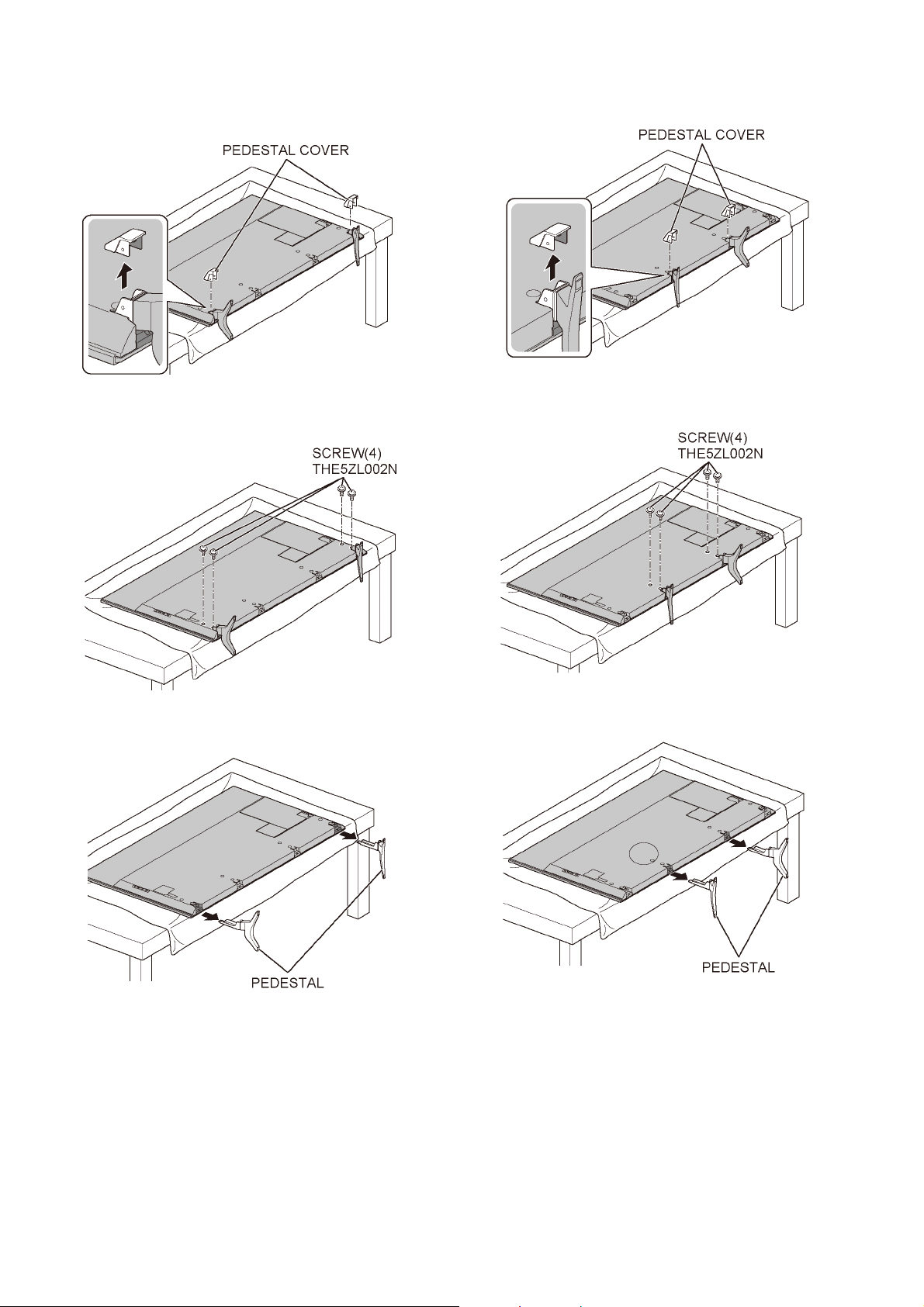
[DX750E]
[Style1]
1. Remove the 2 Pedestal Covers.
[Style2]
1. Remove the 2 Pedestal Covers.
2. Remove the 4 screws.
3. Remove the Pedestal L/R.
2. Remove the 4 screws.
3. Remove the Pedestal L/R.
24
Page 25
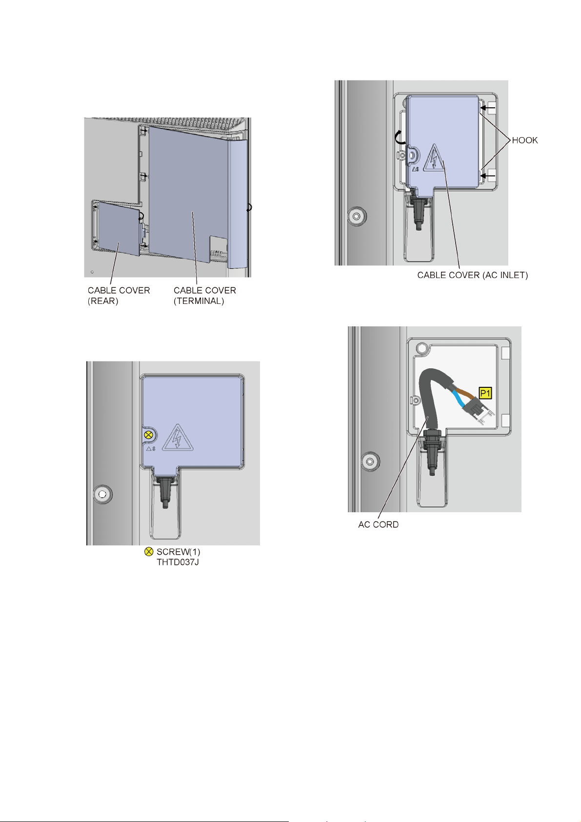
8.2.2. Cable Cover (Terminal) and Cable Cover (Rear)
1. Remove the Cable Cover (Terminal).
2. Remove the Cable Cover (Rear).
8.2.3. AC Cord
1. Remove the 1 screw.
2. Remove the 2 Hooks.
3. Remove the Cable Cover (AC Inlet).
4. Disconnect the connector (P1).
5. Remove the AC Cord.
25
Page 26
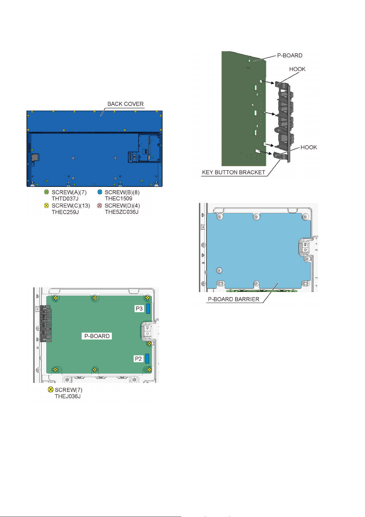
8.2.4. Back Cover
1. Remove the 7 screws (A).
2. Remove the 8 screws (B).
3. Remove the 13 screws (C).
4. Remove the 4 screws (D).
5. Remove the Back Cover.
Caution:
Before removing cover, receiver must be disconnect from
mains.
4. Remove the 2 hooks.
5. Remove the Key Button Bracket.
6. Remove the P-Board Barrier.
8.2.5. P-Board
Caution:
To remove P.C.B. wait 1 minute after power was off for
discharge from electrolysis capacitors.
1. Remove the 7 screws.
2. Disconnect the connectors (P2 and P3).
3. Remove the P-Board.
26
Page 27
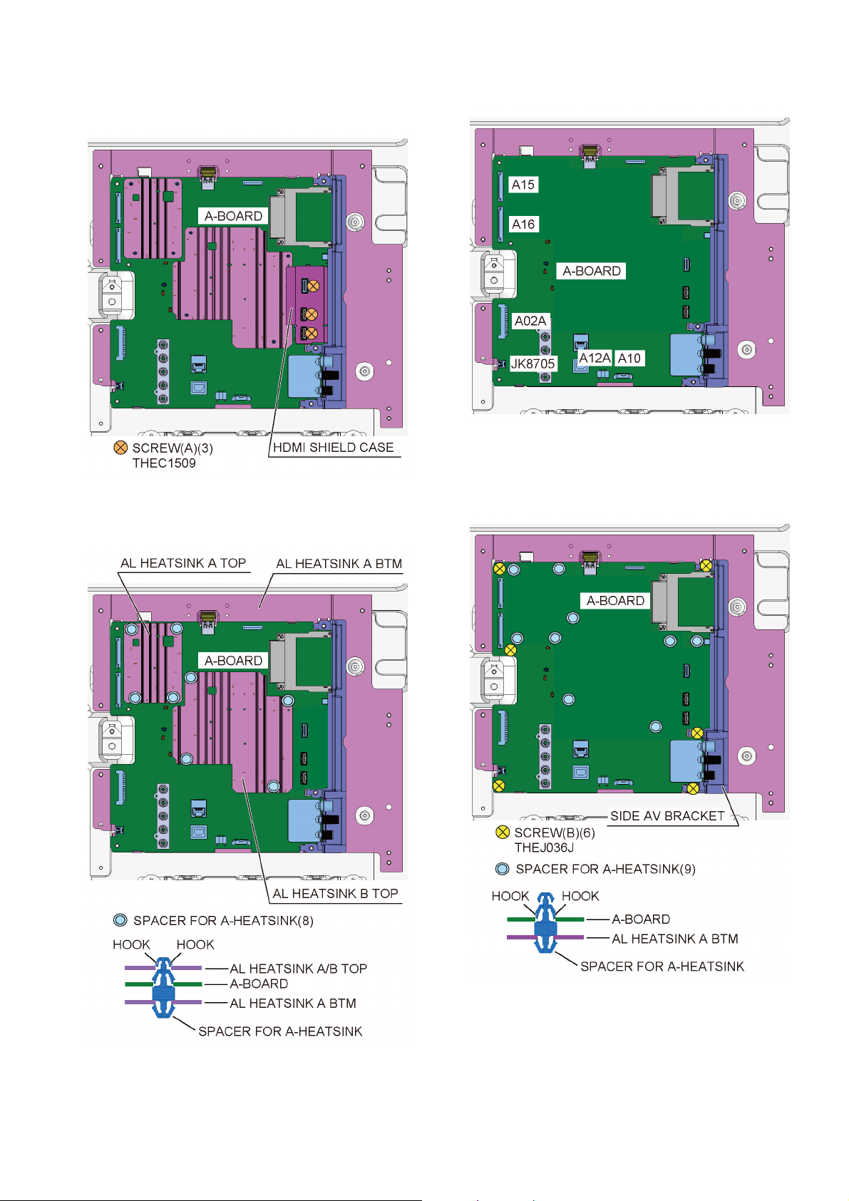
8.2.6. A-Board
1. Remove the 3 screws (A).
2. Remove the HDMI Shield Case.
3. Remove the 82 hooks.
4. Remove the AL Heatsink A Top and AL Heatsink B Top
from 8 Spacer for A-Heatsinks.
5. Disconnect the connectors (A02A, A10, A12A, A15, A16
and JK8705).
6. Remove the 6 screws.
7. Remove the Side AV Bracket.
8. Remove the 92 hooks.
9. Remove the A-Board from 9 Spacer for A-Heatsinks.
27
Page 28
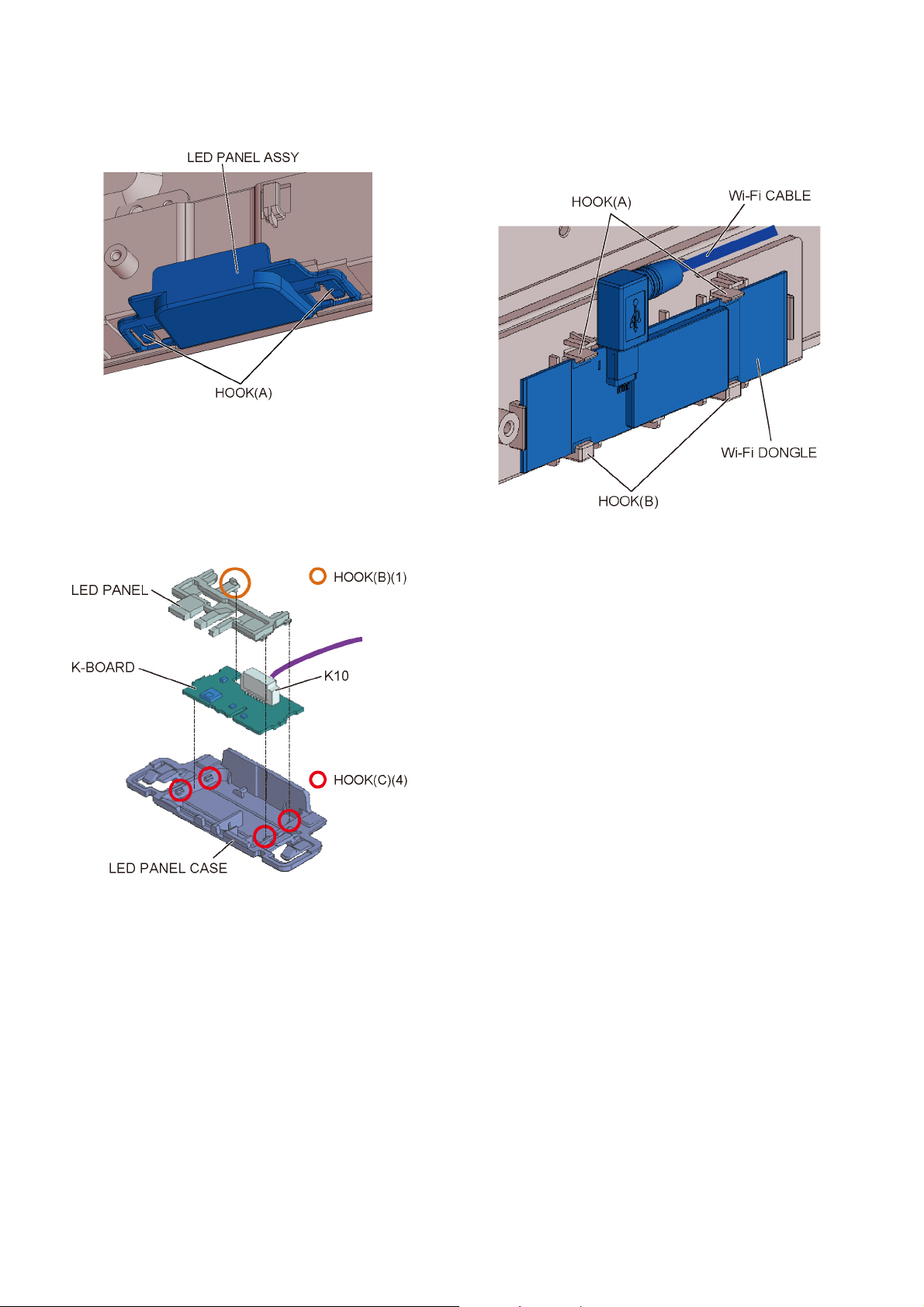
8.2.7. K-Board
1. Remove the 2 hooks (A).
2. Remove the LED Panel Assy.
3. Remove the 1 hook (B).
4. Remove the 4 hooks (C).
5. Remove the K-Board and the LED Panel from the LED
Panel Case.
6. Disconnect the connector (K10).
7. Remove the K-Board from the LED Panel.
8.2.8. Wi-Fi Dongle
1. Disconnect the Wi-Fi Cable.
2. Remove the 2 hooks (A).
3. Remove the 2 hooks (B).
4. Remove the Wi-Fi Dongle.
28
Page 29
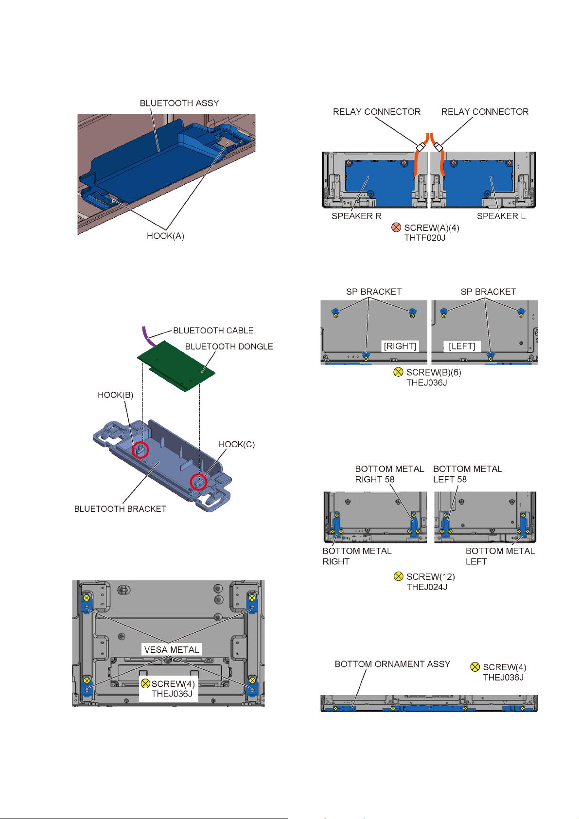
8.2.9. Bluetooth Dongle
1. Remove the 2 hooks (A).
2. Remove the Bluetooth ASSY.
3. Remove the 1 hook (B).
4. Remove the 1 hook (C).
5. Remove the Bluetooth Dongle from Bluetooth Bracket.
6. Remove the Bluetooth Cable.
8.2.11. Speaker L/R
1. Disconnect the 2 relay connectors.
2. Remove the 4 screws (A).
3. Remove the Speaker L/R.
4. Remove the 6 screws (B).
5. Remove the 6 SP Brackets.
8.2.10. VESA Metals
1. Remove the 4 screws.
2. Remove the 4 VESA Metals.
8.2.12. Bottom Metals
1. Remove the 12 screws.
2. Remove the Bottom Metal Left, the Bottom Metal Left 58,
the Bottom Metal Right and the Bottom Metal Right 58.
8.2.13. Bottom Ornament Assy
1. Remove the 4 screws.
2. Remove the Bottom Ornament Assy.
29
Page 30
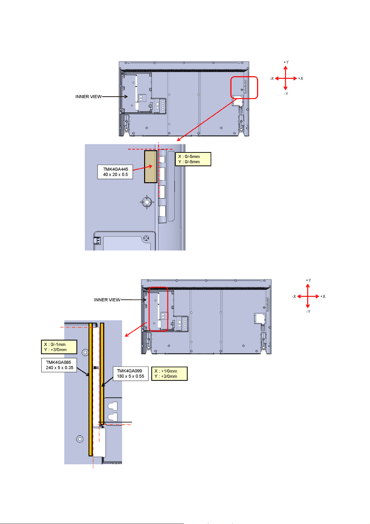
8.3. Countermeasure of Sound vibration specification
8.3.1. FELT on Back Cover (core side KEY BUTTON area)
8.3.2. FELT on Back Cover (core side TERMINAL area) (1)
30
Page 31
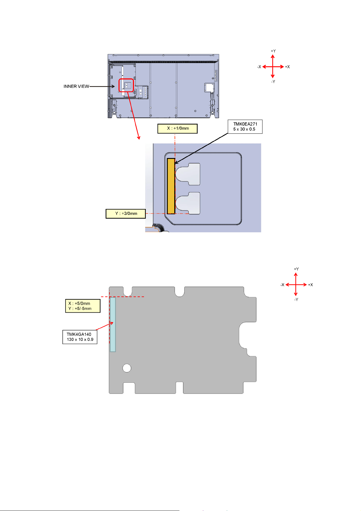
8.3.3. FELT on Back Cover (core side TERMINAL area) (2)
8.3.4. FELT on P-PCB_BARRIER
31
Page 32

8.3.5. Sponge on LCD PANEL
32
Page 33
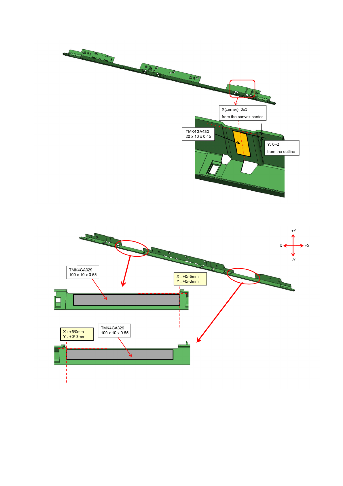
8.3.6. FELT and SPONGE on Bottom ornament
8.3.7. FELT on Bottom ornament
33
Page 34
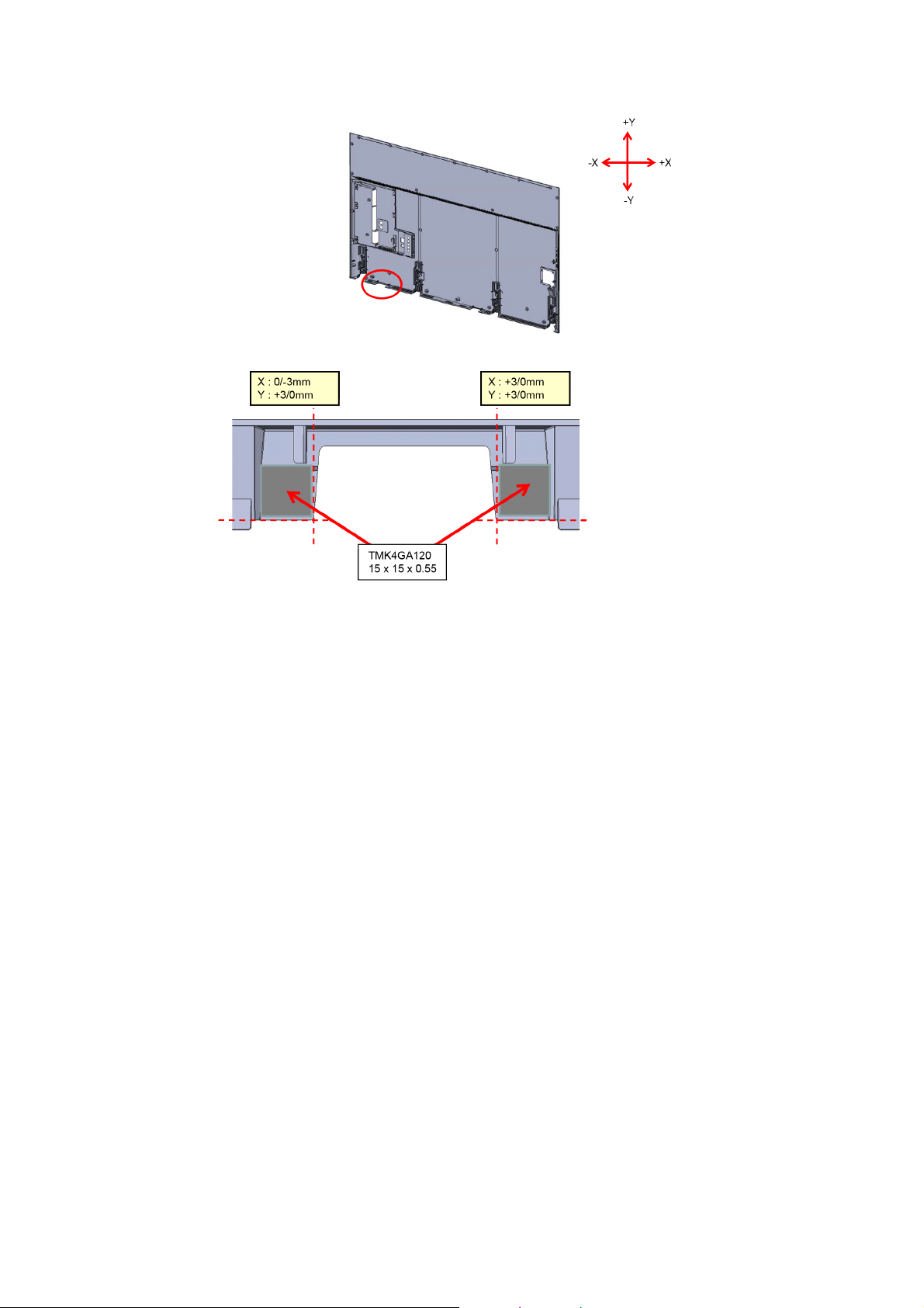
8.3.8. FELT on Back Cover (Blue tooth area)
34
Page 35
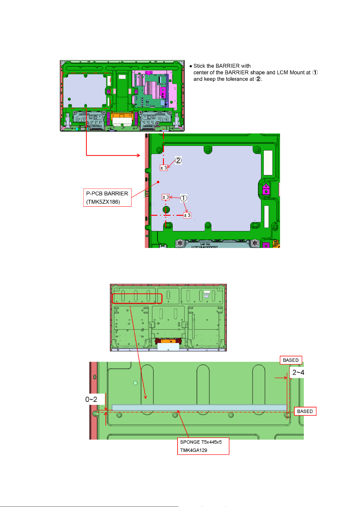
8.4. P-Board Barrier
8.4.1. P-Board Barrier Sticking Specification
8.4.2. SPONGE STICKING
35
Page 36
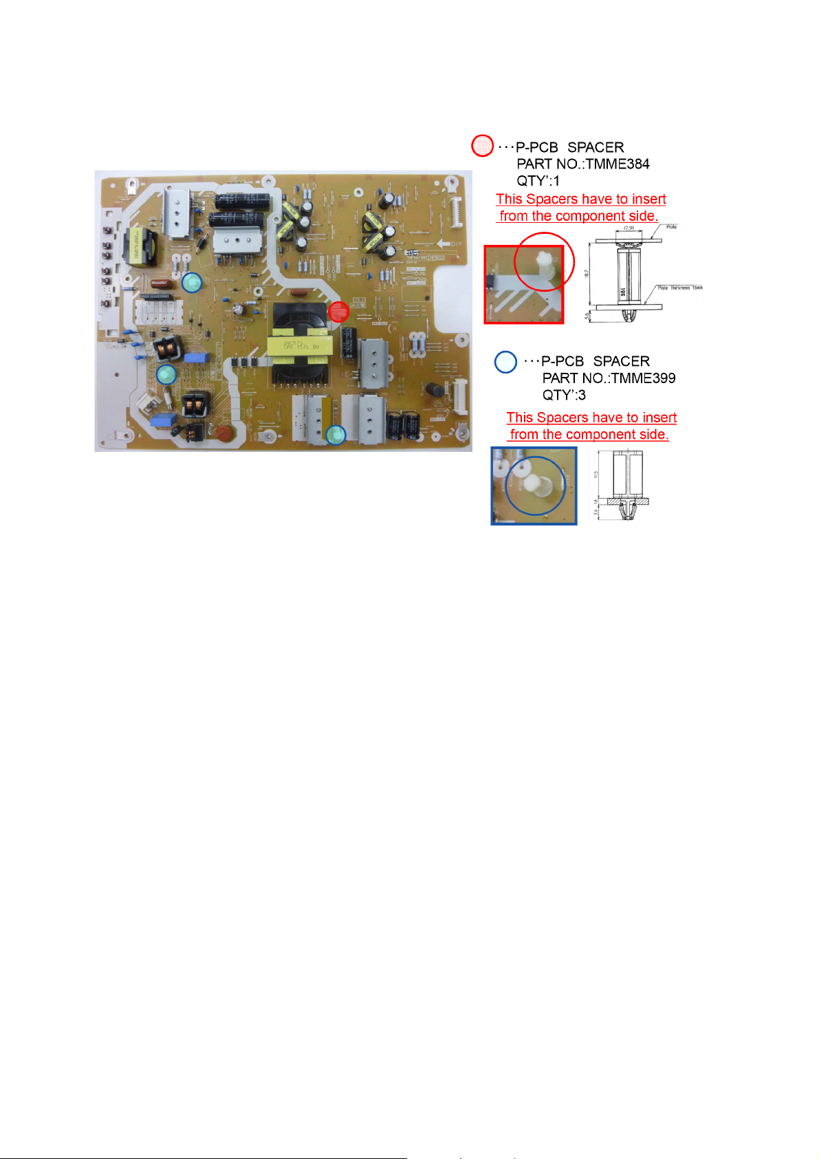
8.5. Spacer
8.5.1. P-Board Spacer
36
Page 37
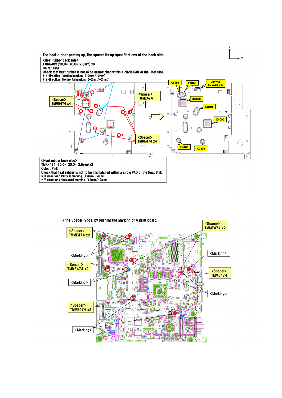
8.6. A-Board radiation of heat specifications
8.6.1. A-Board radiation of heat specifications (1)
8.6.2. A-Board radiation of heat specifications (2)
37
Page 38

8.6.3. A-Board radiation of heat specifications (3)
8.6.4. A-Board radiation of heat specifications (4)
38
Page 39
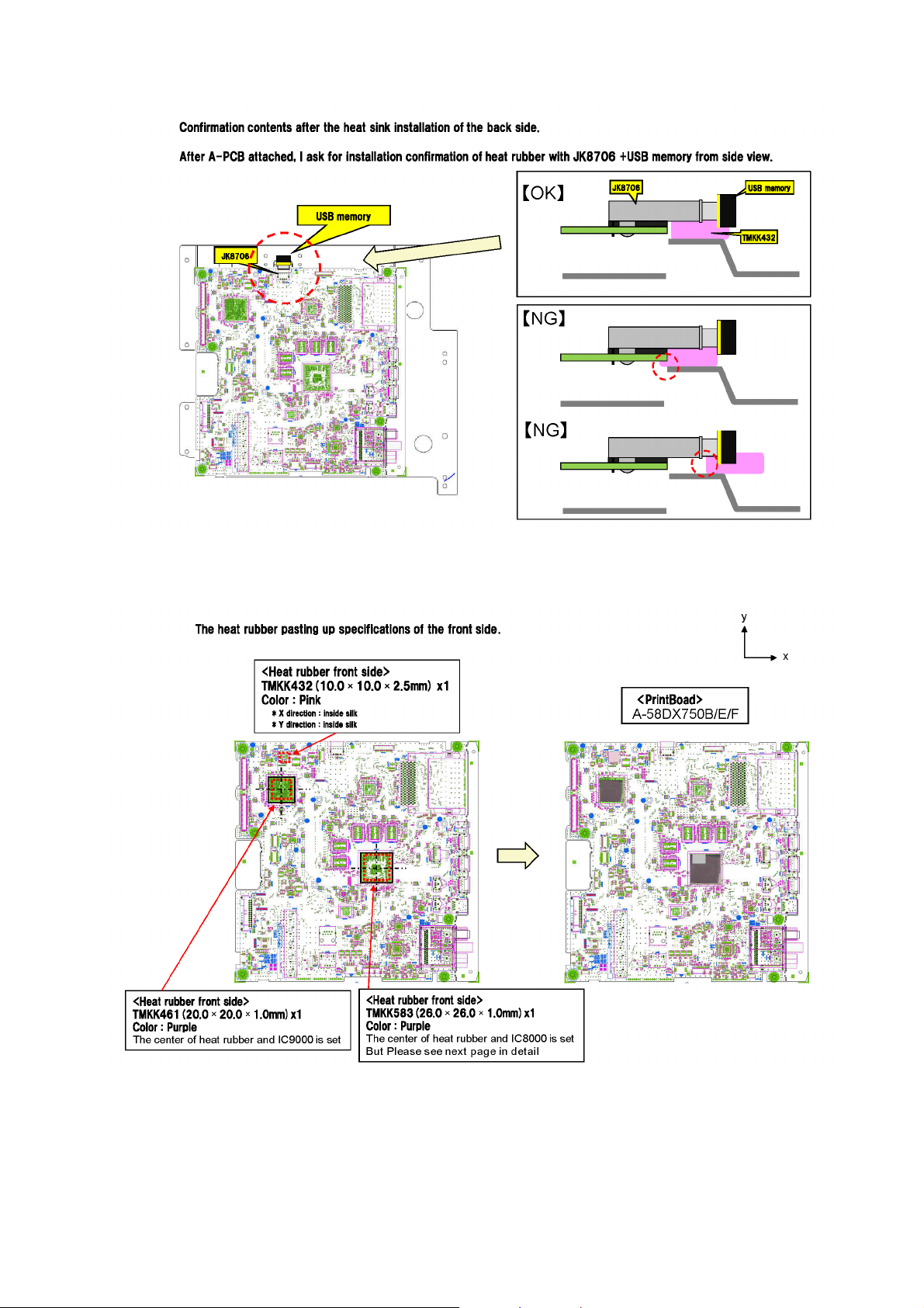
8.6.5. A-Board radiation of heat specifications (5)
8.6.6. A-Board radiation of heat specifications (6)
39
Page 40
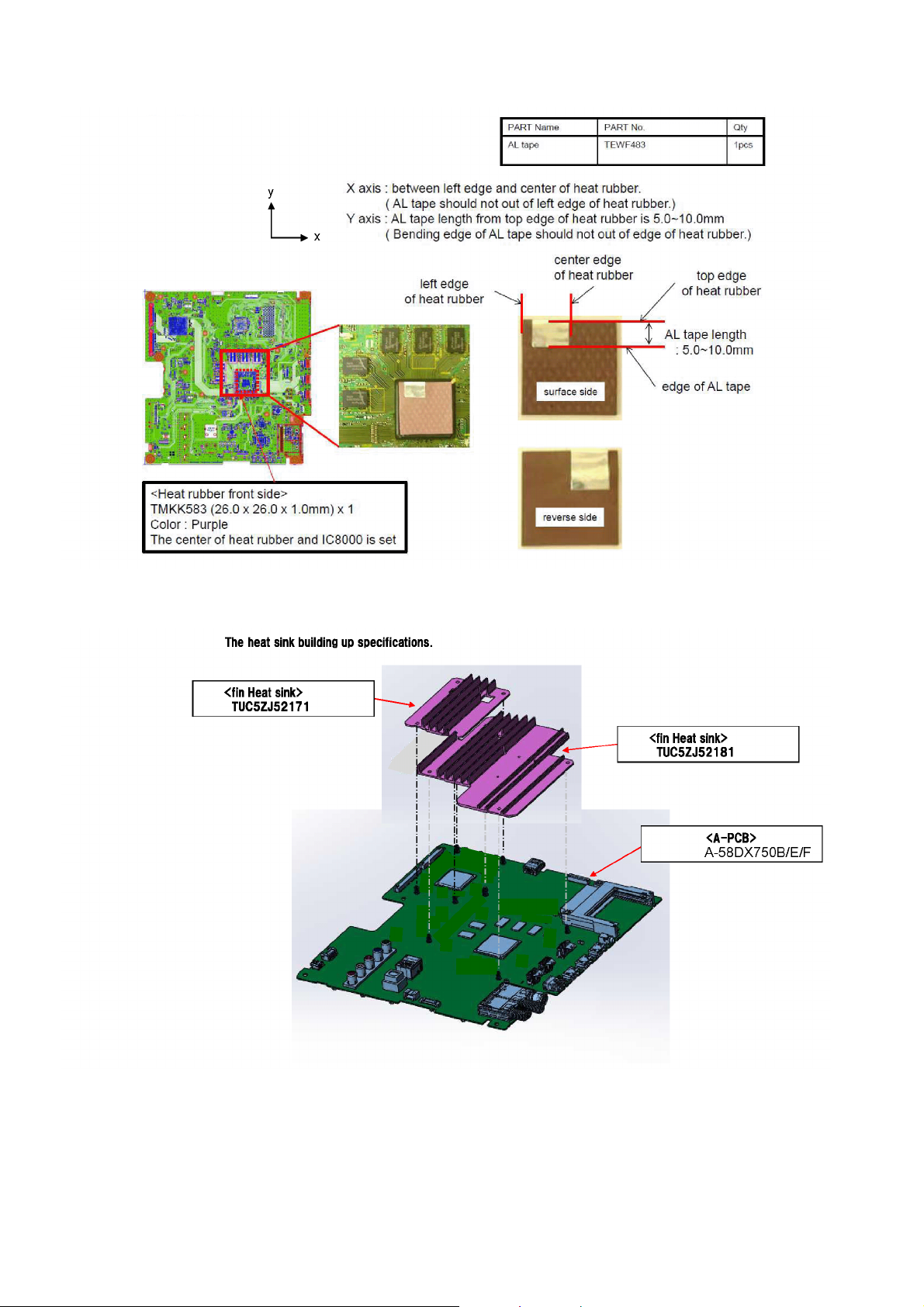
8.6.7. A-Board radiation of heat specifications (7)
8.6.8. A-Board radiation of heat specifications (8)
40
Page 41
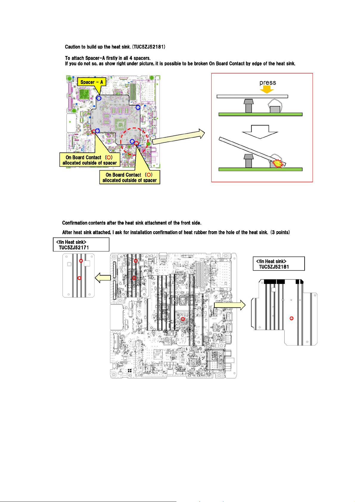
8.6.9. A-Board radiation of heat specifications (9)
8.6.10. A-Board radiation of heat specifications (10)
41
Page 42
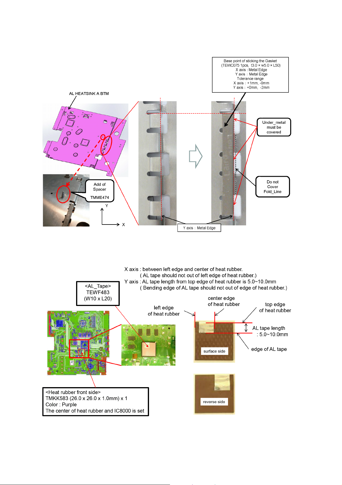
8.7. Specification of EMI countermeasures
8.7.1. Specification of sticking the Gasket (1)
8.7.2. Specification of sticking the rubber
42
Page 43
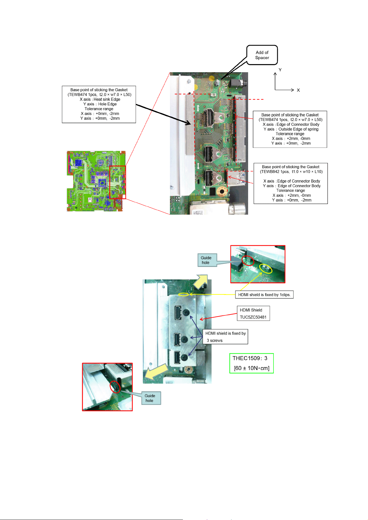
8.7.3. Specification of sticking the Gasket (2)
8.7.4. Specification of HDMI shield case
43
Page 44
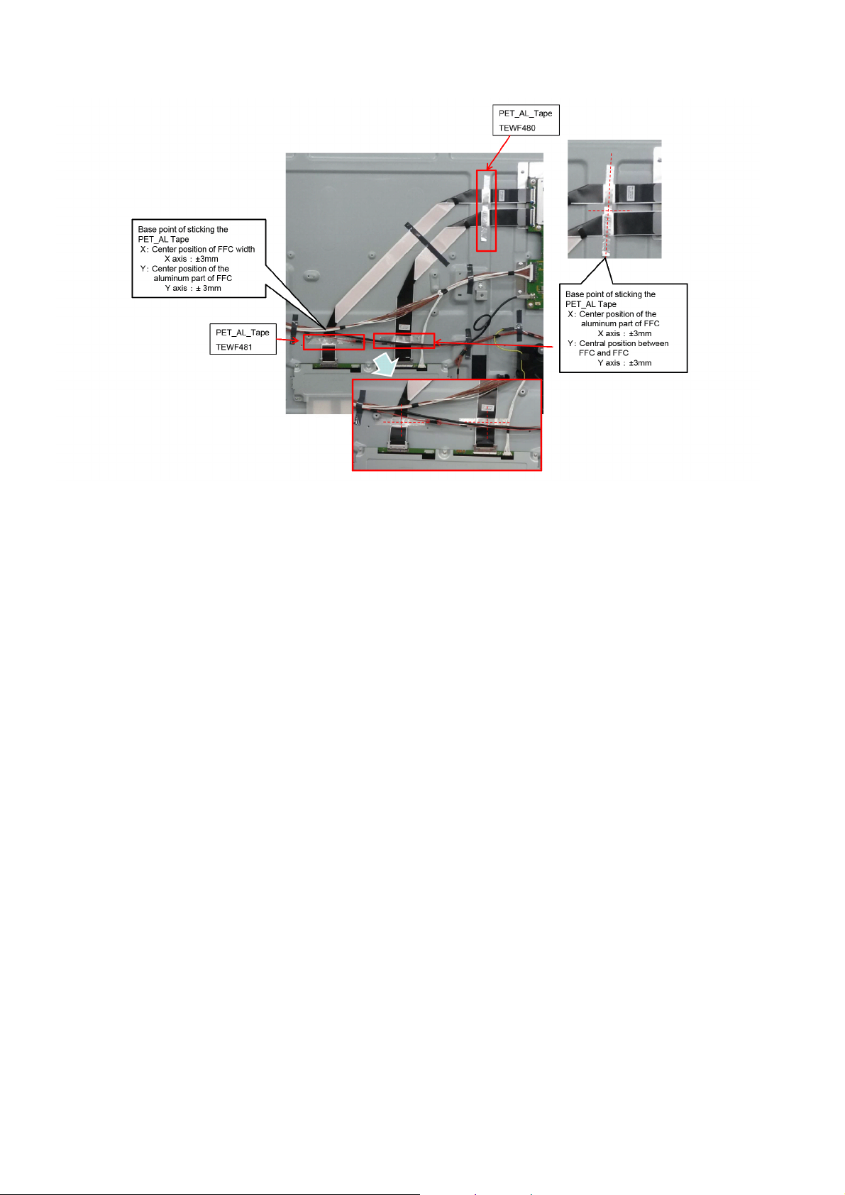
8.7.5. Specification of PET AL Tape
44
Page 45
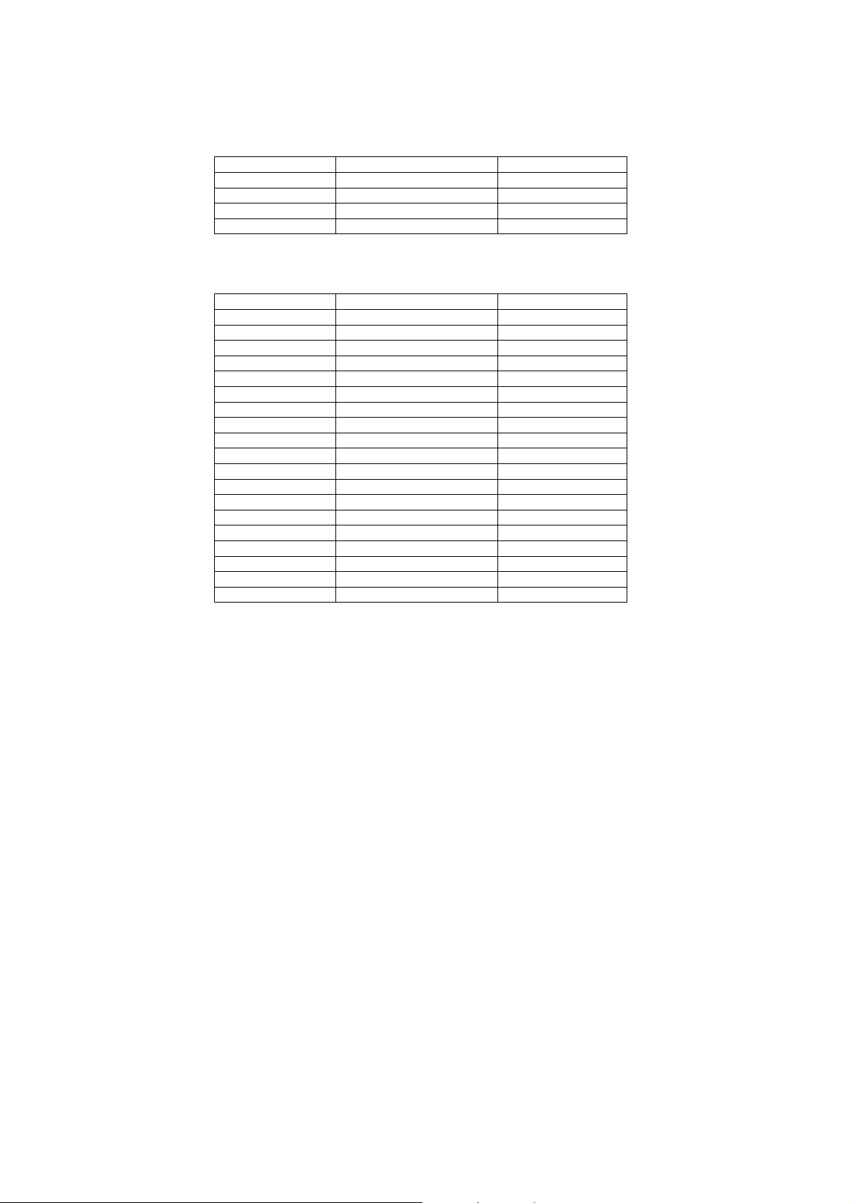
9 Measurements and Adjustments
9.1. Voltage chart of P-board
Power Supply Name Test point Spec
16V TP7410, TP7411, TP7412 16 ± 0.6V
5VS TP7405, TP7420 5.25 ± 0.2V
64V TP7408, TP7409 68V ± 10V
PFC TP7201, TP7402 390V ± 15V *HOT
9.2. Voltage chart of A-board
Power Supply Name Test point Spec
PNL12V TP4059 12V ± 1.2V
USB5V TP5221 5.18V ± 0.25V
USB1 TP8711 5.0V ± 0.25V
USB2 TP8701 5.0V ± 0.25V
USB3 TP8705 5.0V ± 0.25V
USB-WiFi TP8718 5.14V ± 0.20V
USB-4KDEMO TP8724 5.14V ± 0.20V
SUB3.3V TP5201 3.33V ± 0.15V
HDMISW3.3V TP4514 3.35V ± 0.17V
SUB_AI_3.3V TP2206 3.3V ± 0.17V
STB_1.5V TP8101 1.52V ± 0.07V
SUB1.0V TP8100 1.02V + 0.03V - 0.05V
AVDD1.0V TP8102 1.06V ± 0.05V
MSTAR1.5V TP9160 1.50V ± 0.07V
MSTAR0.95V TP9150 1.00V ± 0.07V
WOL3.3V/PHY3.3V TP8606 3.3V ± 0.17V
EU_TU_1.8V TP5704 1.84V ± 0.1V
T2_1.1V TP5705 1.15V ± 0.11V
SUB_CI_5V TP6406 5.0V ± 0.5V
45
Page 46

46
Page 47
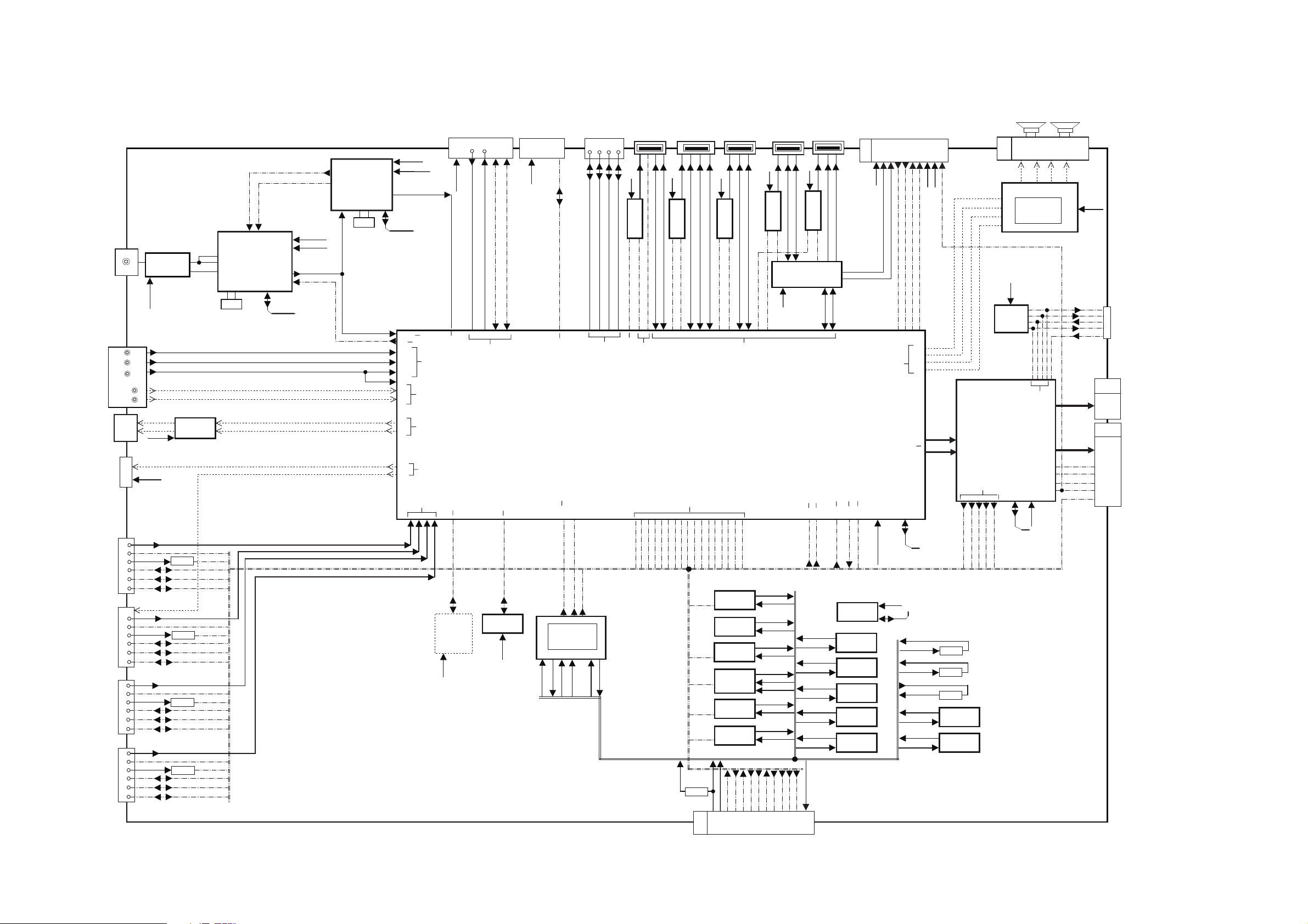
10 Block Diagram
SP_L
SP_R
IC8000
[MT5810PEHJ]
Digital
Audio Out
D3200
ASPDIFO0
SUB3.3V
AB34
G27
ASPDIFO0
ASPDIFO1
Audio
JK4703
HDMI1
HPD2
5VDET2
DDCSDA2
CEC
P2_RX
JK4704
HDMI2
JK4702
HDMI3
R4515
R4521
R4651
DDCSCL2
HPD3
5VDET3
DDCSDA3
CEC
DDCSCL3
HPD1
5VDET1
DDCSDA1
CEC
DDCSCL1
ASPDIFO1
P3_RX
P1_RX
P1_RX
HDMI_2_SDA
HDMI_2_SCL
HDMI_3_SDA
HDMI_3_SCL
2_PWR5V
3_PWR5V
HDMI_1_SDA
1_PWR5V
HDMI_1_SCL
HDMI
Receiver
ETHERNET
JK8600
TX+
TX-
RX+
RX-
1
2
3
6
TX+
TX-
RX+
RX-
ETHERNET
JK8703
USB1
1
2,3 5,6
IC8703
SW
6
1
3
4
USB5V
VBUS2
OCP2
USB_DM(DP)_P2(P,N)
8,9
1
2
3
CEC
6
1
3
4
USB5V
JK8701
USB2
SSUSB_RX(P,N)
SSUSB_TX(P,N)
VBUS0
USB_DM_P0(N)
OCP0
USB_DP_P0(P)
1
2
3
IC8702
SW
6
1
3
4
USB5V
HUB_OC1
USB0DN
JK8702
USB3
IC8705
USB HUB
4
3
25
2
1
VBUS1
USB0DP
USB_DP_P1(N)
USB_DM_P1(P)
1
2
3
IC8706
SW
6
1
3
4
STB5V
JK8705
WIFI
LED_PWM3
USB_DM_P3(N)
OPCTRL18
USB_DM_P3(P)
4
OPCTRL12
Other
Power
USB+GPI0
IC9000
[C1AB00004396]
MSTAR /FRC/
V-By-One RXLVDS
V-By-One TX
A12A
IC3800
[C1AB00003984]
AUDIO AMP
8
7
6
5
1
2 3
4
9,16
25,32
10,11
14,15 26,27
30,31
L- L+
R+
R-
16V
CN0100
SERVICE
Service
SUB5V
IC5911
Temp.Sensor
IIC_1
SUB3.3V
IIC_0
IIC_1
IIC_2
IC5000
[AN34043AAVF]
ANALOG ASIC
1
6 2
14
31
STB5V
STB5V
SUB5V
SUB9V
13
32
STB3.3V
EASTERRST2
8
TV_SUB_ON
DCDCEN
11
CN9300
2
4
6
5
7
FR_GPIO07
FR_CSZ
FR_SDO
FR_SDI
FR_SCK
IC9600
SPI FLASH
1
2
5
6
SUB3.3V
8
FRC
SPI-FLASH
KEY1
P35
SERVO ADC input
POWER ON
L35
SERVO ADC input
BL_ECO
AL36
PWM
AD38
Power
BL_SOS
BL_PWM1
BL_PWM2
BL_PWM3
BL_PWM4
FRC GPI0-IF
V-By-One
Video
A-BOARD
[EXCHANGE UNIT]
AR25
LVDS/EPI/VBI
PANEL_TEST_ON
PANEL_TEST_ON
IC5220
DC/DC
2
8
16V
USB5V
IC4506
Reg
8
1
HDMISW3.3V
IC8100
DC/DC
12,23,26
17
SUB1.0V
IC9150
DC/DC
8
6
MSTAR0.95V
4,5,6
11,12
16V
PNL12V
5
6
STB5V
STB_1.5V
DCDCEN
DCDCEN-2
5
14
DCDCIN
DCDCIN
SUB5V
10,15
DCDCEN
3
SUB5V
IC5200
DC/DC
8
6
16V
SUB3.3V
IC5260
DC/DC
IC8101
DC/DC
USB5V
SUB5V
R5224
8
1
SUB3.3V
AVDD1.0V
3
2,4
SUB3.3V
EU_TU_1.8V
VJ5202
IC8102
Reg
IC5704
Reg
HDMI3.3V
HDMISW3.3V
STB3.3V
PHY3.3V
SUB1.0V
AVDD1.0V
STB_1.5V
SUB3.3V
HDMI3.3V
SD3.3_1.8V
MSTAR0.95V
MSTAR1.5V
MSTAR3.3V
CI SLOT
JK6400A
17,18
51,52
SUB_CI_5V
CI DATA
TS Paraller Output
TS Paraller Input
GPI0, DEMOD
AN30
AM31
AN31
AP36
AUDIO
MCLK
BCLK
LRCLK
SDATA0
2_HPD
3_HPD
1_HPD
P2_RX
P3_RX
P1_RX
P2_RX
P3_RX
CEC
CEC
CEC
IC8701
SW
1
2
3
IC870
7
SW
6
1
3
4
USB5V
HUB_OC2
USB2DN
JK8706
4K-DEMO
(shop mode)
USB2DP
VBUS3
24
VBUS1
VBUS3
7
6
USB5V
TV_SUB_ON
AB38
Power
EASTERRST2
M34,R36
FRC GPI0
BL_ON
IIC_0
V-By-One
OSD
DCDCEN-2
1
IC9160
DC/DC
2
3
MSTAR1.5V
DCDCIN
DCDCEN-2
7
2
3
SUB5V
1
5
SUB5V
IC5705
DC/DC
DMD_1.2/1.1V
IC6405
Reg
SUB_CI_5V
4
5
STB5V
IC8601
Reg
PHY3.3V
JK4701A
HDMI4
R4545
HPD0
5VDET0
DDCSDA0
CEC
DDCSCL0
HDMI_0_SDA
0_PWR5V
HDMI_0_SCL
0_HPD
CEC
P0_RX
P0_RX
3
7
9-10
12
A02A
TO P2/TCON
9
10
1-4,13
15
7
STB5V
BL_ECO
BL_ON
17
TV_SUB_ON
16V
19
BL_PWM1
BL_SOS
18
21
BL_PWM2
22
BL_PWM3
BL_PWM4
8
KEY1
16
VJ2000
DCDCIN
POWER ON
26-28
PNL12V
16V
DDR3 _ 5X4GB
IC8200
IC8201
IC8202
IC8203
IC8204
DDR
STB1.5V
IC8920
eMMC 4GB
SUB3.3V
eMMC
Y35
U37
AA34
AA33
A10
4
12
3
9
TO K10/Bluetooth
10 7 6
2
SUB3.3V
8
R_LED_ON
G_LED_ON
AI_SENSOR
REMOTE
SUB3.3V
STB3.3V
BT_USB_DN
BT_USB_DP
1
3D_LROUT
15
16
BT_USB_DN
BT_USB_DP
V-By-One TX
18,19,21,22
24,25,27,28
30,31,33,34
36,37,39,40
A15
TO PANEL
2,3,5,6
8,9,11,12
14,15,17,18
20,21,23,24
TO PANEL
A16
V-By-One
V-By-One
26
27
35
PANEL_3D_ON
29
VTX_LOCK
VTX_HTP
36
PANEL_TEST_ON
3D_LROUT
1_HPD
1_PWR5V
HDMI_1_SDA
HDMI_1_SCL
HDMI_CEC
2_HPD
2_PWR5V
HDMI_2_SDA
HDMI_2_SCL
3_HPD
3_PWR5V
HDMI_3_SDA
HDMI_3_SCL
HDMI
0_HPD
0_PWR5V
HDMI_0_SDA
HDMI_0_SCL
AA6
Y6
AJ21
AJ28
DEMOD
F37,F38
Demod
B14
Demod
38,37
IIC_2
DMD_1.2/1.1V
SUB3.3V
48
IC6800
[C1AB00004028]
DVB-T/T2/C DEM
3,4,5,8
34
35
X6800
AGC1
FEF_FLAG
47
20,21
45,46
DMD_0_T
IF2_N,P
TSVAL
TSSYNC
TSCLK
TSDATA0
AGC2
IF2_N,P
SUB3.3V
JK6951
IC6952
LNA
4
1
3
6
IC6950
22
24
RF_IP
RF_IN
20
[C1AB00004337]
Digital and Analog
TV Tuner
SUB3.3V
TU_1.8V
9,15,17,23
7
IF2_N,P
10,11
2,3
13
14
X6950
AGC2
4
AGC1
5
FEF_FLAG
1
DMD_0_T
P0_RX
Analog Video input
LIN_TERMINAL
COMP_D_PR
COMP_D_PB
COMP_D_Y
RIN_TERMINAL
JK3101
Y/Vin,PB,PR
AUDIO
IN
L
R
COMP_D_Y
COMP_D_PR
COMP_D_PB
J37
K36
D37
B36
Audio Line in ADC
LIN_TERMINAL
RIN_TERMINAL
Audio DAC
HP_L
JK3104A
HP_R
HP-OUT
IC3201
Stereo HP
Driver
9
11
13
15
SUB3.3V
C35
D36
HP_L
HP_R
L36,L37
K37
J38
CVBS3P
SUB3.3V
SD3.3_1.8V
VJ5002
10.1. Block Diagram (1/2)
47
Page 48
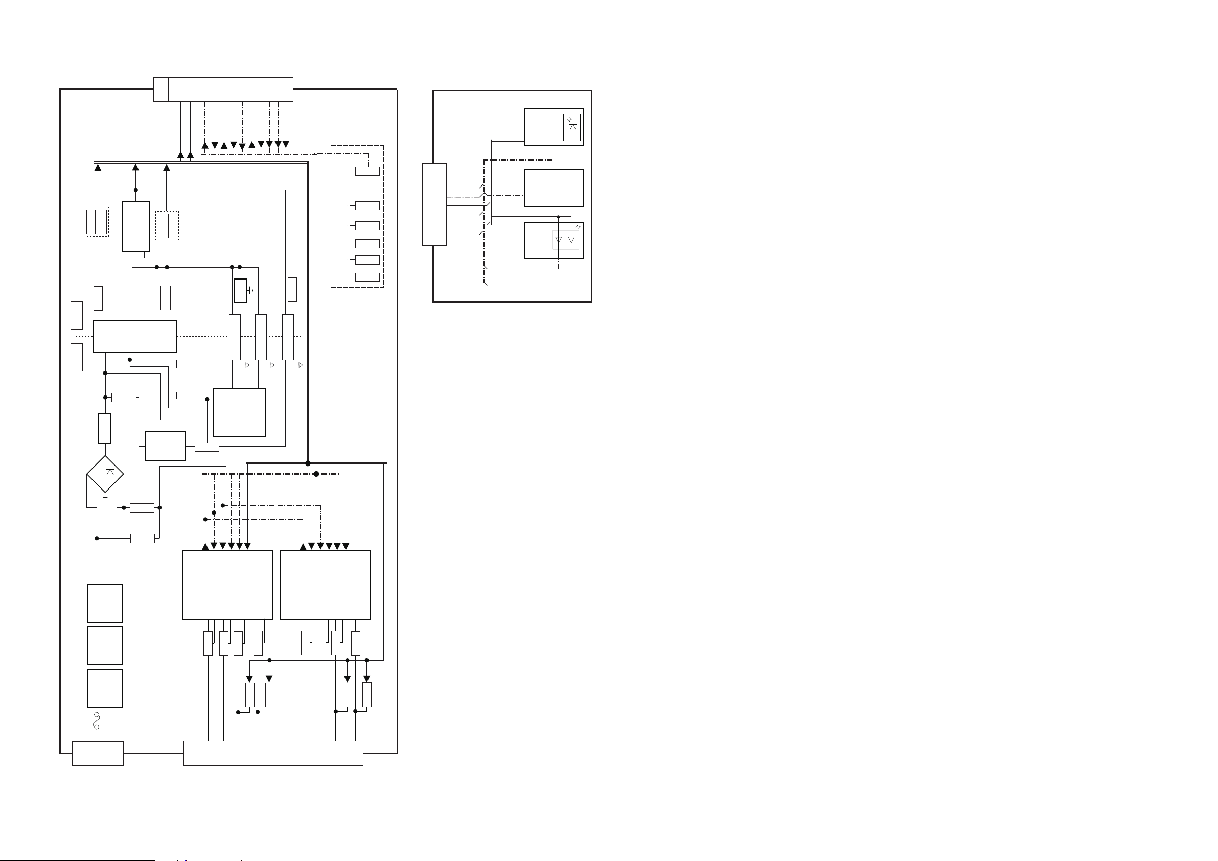
LF7104
F7101
KEY CONTROL
~
~
+
-
D7100
D7104
D7105
IC7301
14VS
8VW
Resonant
Controller
HOT
COLD
PC7301
Photo coupler
1
VH
4FB
5VS
P2
TO A02A
9
SUB_ON
POWER_ON
10
7
1-4,13
8
KEY
IC7401
MAIN INPUT
LF7105
T7202
2
4
IC7201
PFC
Control IC
7OUT
8VCC
Q7203
Q7202
3
T7302
PC7303
Photo coupler
PC7302
Photo coupler
64V
16V
SUB_ON
16V
9 PGS
10VCC
4
D7304
10,5
12
7
D7403
D7412
D7416
Q7401
P-BOARD
Line Filter
LF7103
Line Filter
Line Filter
IC7405
DC/DC
2
8
SW2855
SW2854
SW2853
SW2852
SW2851
KEY
SW2857
POWER_ON
P3
6
TO PANEL
8
1
2
Q7403
Q7405
BL_PWM1
17
BL_ON
18
BL_SOS
16
CATHODE1
ANODE1
5VS
3 EN
K-BOARD
K10
2
5
4
3
1
7
STBY 3.3V
SUB3.3V
RM2800
VCC
OUT
SN2800
AI
2
4
VCC
OUT
D2802
R
G
TO A10
REMOTE
AI
G LED
R LED
SUB3.3V
AI
STBY 3.3V
STBY 3.3V
R LED
G LED
REMOTE
15
BL_ECO
BL_PWM2
19
BL_PWM3
21
BL_PWM4
22
IC7800
LED DRIVER
DC/DC
2
STB
12FAIL
20DIMOUT2
BL_SOS
BL_ON
BL_PWM3
11PWM2
19ISENSE2
Q7802
Q7803
9ADIM
BL_ECO
BL_PWM4
10PWM1
CATHODE2
6
DIMOUT1
7ISENSE1
Q7804
4GATE1
3CS1
ANODE2
Q7801
22GATE2
23CS2
L7814
L7813
10
12
3
4
CATHODE3
ANODE3
IC7900
LED DRIVER
DC/DC
2
STB
12FAIL
20DIMOUT2
BL_PWM1
11PWM2
19ISENSE2
Q7901
Q7902
BL_PWM2
10PWM1
CATHODE4
6
DIMOUT1
7ISENSE1
Q7903
4GATE1
3CS1
ANODE4
Q7900
22GATE2
23CS2
L7911
L7910
64V
64V
16V
1VCC
16V
1VCC
64V
64V
64V
P1
1
2
Q7404
Q7402
9ADIM
10.2. Block Diagram (2/2)
48
Page 49
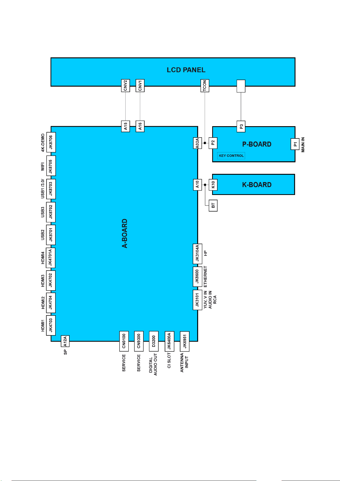
11 Wiring Connection Diagram
11.1. Wiring Diagram
49
Page 50
11.2. Caution statement.
Caution:
Please confirm that all flexible cables are assembled correctly.
Also make sure that they are locked in the connectors.
Verify by giving the flexible cables a very slight pull.
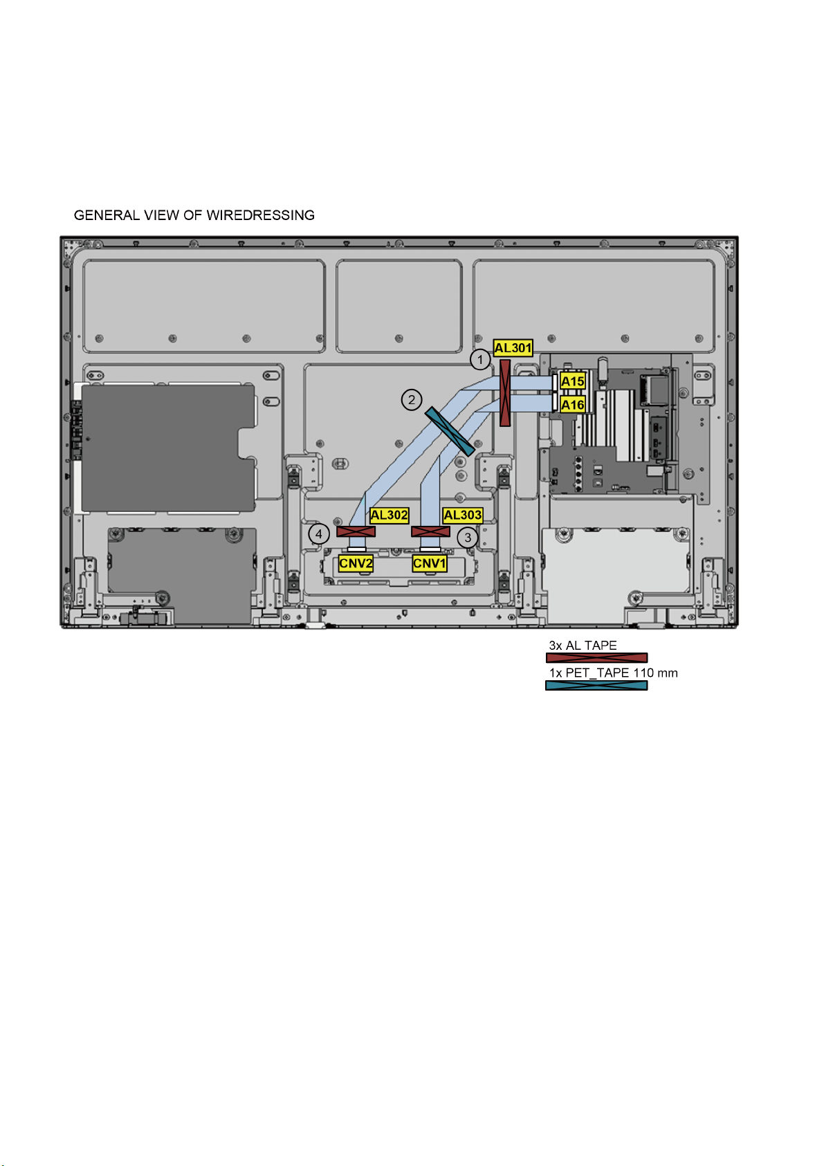
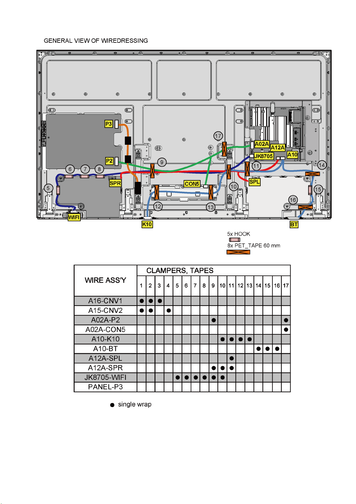
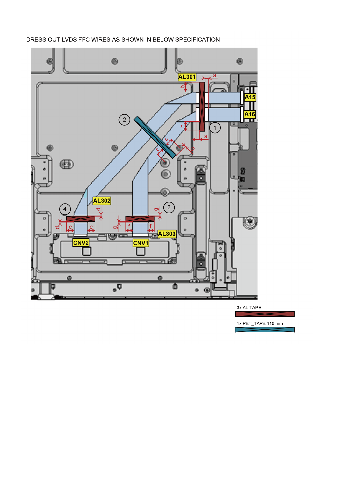
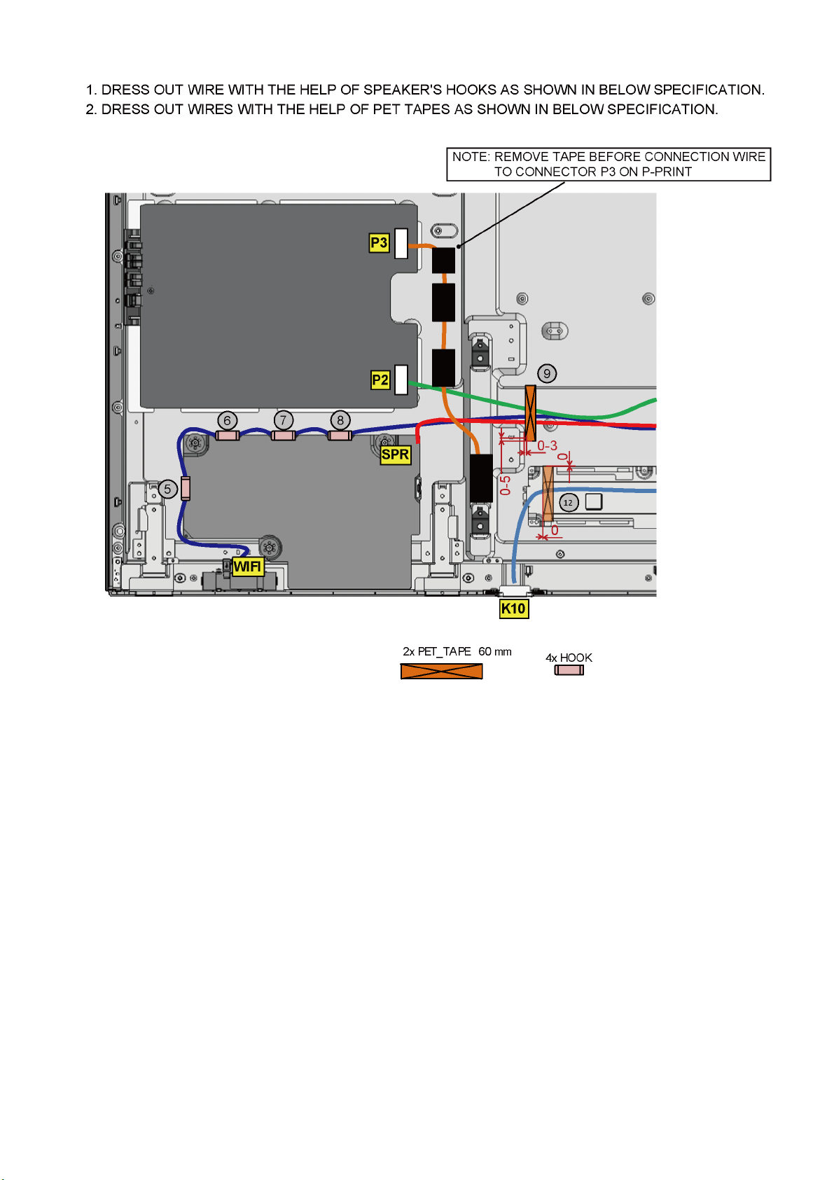
11.3. Dressing Wire
50
Page 51
5152535455
Page 52
Page 53
Page 54
Page 55

12 Schematic Diagram
Please click the radio button for "Diagrams II / Parts List" on the menu bar in XML Service Manual.
If you want to print, please click the icon button for "Print" on the icon bar and select the item.
13 Printed Circuit Board
Please click the radio button for "Diagrams II / Parts List" on the menu bar in XML Service Manual.
If you want to print, please click the icon button for "Print" on the icon bar and select the item.
14 Exploded View and Replacement Parts List
Please click the radio button for "Diagrams II / Parts List" on the menu bar in XML Service Manual.
If you want to print, please click the icon button for "Print" on the icon bar and select the item.
 Loading...