


SPECIFICATIONS
Power Source: 220-240V a.c., 50Hz
Power Consumption: 125W
Stand-by Power
Consumption: 2.8W
Aerial Impedance: 75Ω unbalanced, Coaxial Type
Receiving System: PAL I, PAL-525/60
M.NTSC
NTSC (AV only)
Receiving Channels: UHF E21-E69
Intermediate Frequency:
Video/Audio
Video 39.5MHz
Audio 33.5MHz
32.95MHz (NICAM)
Colour 35.07MHz
Terminals:
AUDIO MONITOR OUT Audio (RCAx2) 500mV rms 1kΩ
AV1 IN Video (21 pin) 1V p-p 75Ω
Audio (21 pin) 500mV rms 10kΩ
RGB (21 pin)
AV1 OUT Video (21 pin) 1V p-p 75Ω
Audio (21 pin) 500mV rms 1kΩ
AV2 IN Video (21 pin) 1V p-p 75Ω
Audio (21 pin) 500mV rms 10kΩ
S-Video IN Y: 1V p-p 75Ω
(21-pin) C: 0.3V p-p 75Ω
AV2 OUT Video (21 pin) 1V p-p 75Ω
Audio (21 pin) 500mV rms 1kΩ
Selectable output (21 pin)
ORDER No. SM-01004
Colour Television
TX-32PG30
EURO-7 Chassis
AV3 IN S-Video IN Y: 1V p-p 75Ω
(4-pin) C: 0.3V p-p 75Ω
Audio (RCAx2) 500mV rms 10kΩ
Video (RCAx1) 1V p-p 75Ω
AV4 IN Video (21 pin) 1V p-p 75Ω
Audio (21 pin) 500mV rms 10kΩ
S-Video IN Y: 1V p-p 75Ω
(21-pin) C: 0.3V p-p 75Ω
RGB (21 pin)
AV4 OUT Video (21 pin) 1V p-p 75Ω
Audio (21 pin) 500mV rms 1kΩ
High Voltage: 32kV ± 1kV
Picture Tube: W76EKW10X72 76cm
Audio Output: Left/Right 2 x 20W
(Music Power) 8Ω Impedance
Headphones: 8Ω Impedance
3.5mm
Accessories
supplied : Remote Control
2 x R6 (UM3) Batteries
VS-32PG50 Video Cabinet
Dimensions:
Height: 576mm
Width: 777mm
Depth: 532mm
Net weight: 56kg
Specifications are subject to change without notice.
Weights and dimensions shown are approximate.
NOTE: This Service Manual should be used in conjunction with
the EURO-7 Technical guide.
Panasonic CS ( U.K. ) Ltd.
WILLOUGHBY ROAD,
BRACKNELL,
BERKS.,
RG12 8FT.
CONTENTS
SAFETY PRECAUTIONS..........................................................................................................................................................2
SERVICE HINTS.......................................................................................................................................................................3
SERVICE POSITION.................................................................................................................................................................4
ADJUSTMENT PROCEDURE AND FACTORY SETTINGS.....................................................................................................5
WAVEFORM PATTERN TABLE...............................................................................................................................................6
ALIGNMENT SETTINGS...........................................................................................................................................................7
BLOCK DIAGRAMS..................................................................................................................................................................8
PARTS LOCATION.................................................................................................................................................................13
REPLACEMENT PARTS LIST................................................................................................................................................14
SCHEMATIC DIAGRAMS.......................................................................................................................................................28
CONDUCTOR VIEWS.............................................................................................................................................................36
SAFETY PRECAUTIONS
GENERAL GUIDE LINES
1. It is advisable to insert an isolation transformer in the
a.c. supply before servicing a hot chassis.
2. When servicing, observe the original lead dress in the
high voltage circuits. If a short circuit is found, replace
all parts that have been overheated or damaged by
the short circuit.
3. After servicing, see that all the protective devices
such as insulation barriers, insulation papers, shields
and isolation R-C combinations are correctly
installed.
4. When the receiver is not being used for a long period
of time, unplug the power cord from the a.c. outlet.
5. Potentials as high as 33kV are present when this
receiver is in operation. Operation of the receiver
without the rear cover involves the danger of a shock
hazard from the receiver power supply. Servicing
should not be attempted by anyone who is not
familiar with the precautions necessary when working
on high voltage equipment. Always discharge the
anode of the tube.
6. After servicing make the following leakage current
checks to prevent the customer from being exposed
to shock hazard.
LEAKAGE CURRENT COLD CHECK
1. Unplug the a.c. cord and connect a jumper between
the two prongs of the plug.
2. Turn on the receiver’s power switch.
3. Measure the resistance value with an ohmmeter,
between the jumpered a.c. plug and each exposed
metallic cabinet part on the receiver, such as screw
heads, aerials, connectors, control shafts etc. When
the exposed metallic part has a return path to the
chassis, the reading should be between 4M ohm and
20M ohm. When the exposed metal does not have a
return path to the chassis, the reading must be
infinite.
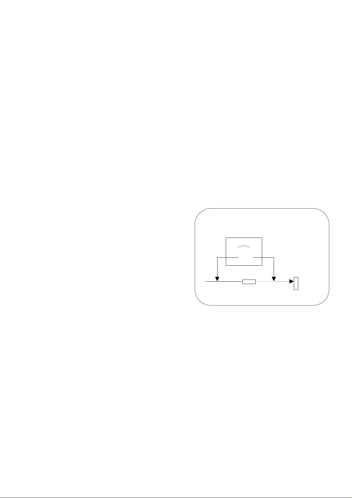
LEAKAGE CURRENT HOT CHECK
1. Plug the a.c. cord directly into the a.c. outlet. Do not
use an isolation transformer for this check.
2. Connect a 2kΩ 10W resistor in series with an
exposed metallic part on the receiver and an earth,
such as a water pipe.
3. Use an a.c. voltmeter with high impedance to
measure the potential across the resistor.
4. Check each exposed metallic part and check the
voltage at each point.
5. Reverse the a.c. plug at the outlet and repeat each of
the above measurements.
6. The potential at any point should not exceed
1.4V rms. In case a measurement is outside the limits
specified, there is a possibility of a shock hazard, and
the receiver should be repaired and rechecked before
it is returned to the customer.
HOT CHECK CIRCUIT
a.c. VOLTMETER
2kΩ 10 Watts
TO INSTRUMENT’S EXPOSED
METALLIC PARTS
Fig. 1.
X-RADIATION WARNING
1. The potential sources of X-Radiation in TV sets are
the high voltage section and the picture tube.
2. When using a picture tube test jig for service, ensure
that the jig is capable of handling 33kV without
causing X-Radiation.
NOTE: It is important to use an accurate periodically
calibrated high voltage meter.
1. Set the brightness to minimum.
2. Measure the high voltage. The meter should indicate.
32kV ± 1kV.
If the meter indication is out of tolerance, immediate
service and correction is required to prevent the
possibility of premature component failure.
3. To prevent any X-Radiation possibility, it is essential
to use the specified tube.
WATER PIPE
(
EARTH)
2
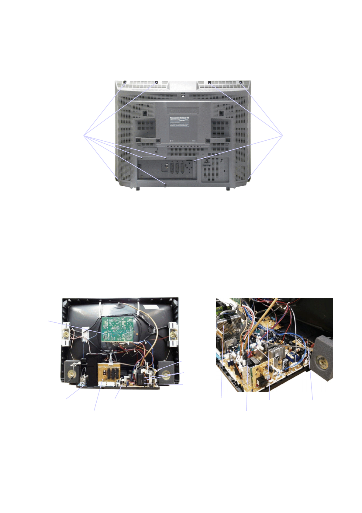
SERVICE HINTS
Focus
Screen
How to remove the rear cover
1. Remove the 10 screws as shown in Fig.2.
SCREWS
LOCATION OF CONTROLS
SCREWS
Fig.2.
L-Board
A-Board
H-Board
D-Board
DF-Board
Fig.3.
3
DG-Board
U-Board
G-Board
K-Board
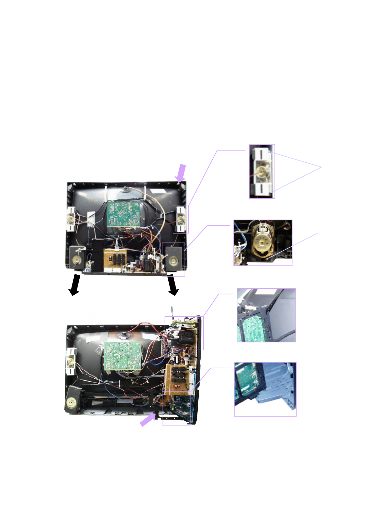
HOW TO MOVE THE CHASSIS INTO SERVICE POSITION
(C)
(D)
(A)
(B)
1. Remove the 3 screws (B) and (C) shown in Fig.5. / Fig.6., and remove the 2 speakers from the cabinet.
2. Affix the support strap supplied in the service pack (TZS1EK002) using a back cover screw, into the top right-hand
cabinet rib (A) shown in Fig.4.
3. Hold and lift the rear of the chassis and gently pull toward you, as shown in Fig.4.
4. Release the respective wiring clips and rotate the chassis vertically through 90°, anti-clockwise.
5. Locate the base of the chassis frame into location (D), shown in Fig.7. / Fig.9.
6. Clip the chassis frame onto the support strap, shown in Fig.7. / Fig.8.
7. After servicing replace the speakers, and ensure all wiring is returned to it’s original position before returning the receiver
to the customer
Fig.5.
Fig.4.
Fig.7.
Fig.6.
Fig.8.
Fig.9.
4

ADJUSTMENT PROCEDURE
Item / Preparation Adjusment/Confirmation
+B SET-UP
4. Receive a Window pattern.
5. Set the controls :Brightness Minimum
Contrast Minimum
Volume Minimum
CUT OFF
1. Receive a Window pattern.
2. Degauss the tube externally.
3. Set the TV into Service Mode 1.
4. Select Sub brightness mode.
Confirm the following voltages.
A - Board
A1 Pin2 7.5 ± 0.5V IC1252 Pin2 2.5 ± 0.25V
A1 Pin12 -20 ± 0.5V IC1251 Pin3 3.3 +0.3 / -0.2V
A1 Pin16 20 ± 0.5V IC3302 Pin3 12 ± 0.6V
A2 Pin15 30 ± 0.5V IC2707 Pin3 8 ± 0.4V
A2 Pin6 15 ± 0.5V L2707 (IC2708) 9 ± 0.4V
A3 Pin4 15 ± 0.5V L2704 (IC2706) 5 ± 0.2V
A3 Pin2 -15 ± 0.5V L2716 (IC2705) 3.3 ± 0.2V
D – Board
TPD8-GND 7.5 ±0.5V
TPD9-TPD11 38.5 ± 2V
TPD10-GND 15.5 ± 1V
TPD13-GND 14.5 ± 1V
TPD15-GND 144.8 ± 1V
TPD32-GND 209 ± 10V
C864-GND -15.5 ± 1V
D2 Pin15-GND 31 ± 1V
To adjust Cutoff connect an oscilloscope to the Blue cathode. Adjust "Cutoff"
value using the "Yellow" and "Blue" buttons until the black level is 170V ± 5V,
press "STR" to store the value. Remove the oscilloscope.
Select Highlight/Lowlight mode press "5" to collapse the screen and adjust the
screen “VR” until the display is just visible, press "5" to return to service mode.
Using the "Yellow" and "Blue" buttons adjust until optimum picture white
balance is achieved, press "STR " to store the value. Select Sub Brightness
mode and adjust until optimum picture brightness is achieved.
L2717 (IC2709) 3.3 ± 0.2V
FACTORY SETTINGS
To return customer settings to factory settings and clear owner ID of all information input by the customer, enter Self-Check
mode. Press the down (-/v) button on the customer controls at the front of the TV set, at the same time pressing the STATUS
button on the remote control. To exit Self Check, switch off the TV set at the power button.
NOTE: Self Check should only be used when refurbishing the TV set and not during normal repair work.
MEM : O.K.
GC1 : O.K.
GC2 : - VDU : O.K.
CIP : O.K.
RGB : O.K.
AVSW : O.K.
Tun1 : O.K.
Tun2 : - DAC1 : O.K.
MSP : O.K.
DOLBY : - CODEC : - DAC2 : - DAC3 : - -
Sum : ****
OPTION 1 : 01
OPTION 2 : 00
OPTION 3 : 10
OPTION 4 : 10
OPTION 5 : 00
OPTION 6 : 50
OPTION 7 : 80
OPTION 8 : 41
OPTION 9 : 00
OPTION 10 : 80
OPTION 11 : 19
OPTION 12 : 08
OPTION 13 : FA
Check : CD
Factory use only
If the CCU ports have been checked and found to be incorrect or not located then " - - " will appear in place of "O.K.".
5

WAVEFORM PATTERN TABLE
Note: All waveforms have been taken using a standard colour bar pattern.
Video Out
IC3001 Pin 56
2.2V
Vert Out
IC451 Pin 3
88V
HFLB
A3 Pin 11
10mS
64µS
Luminance In
IC1315 Pin 37
0.9V
VFLB
IC451 Pin 6
1V
R - Out
IC1315 Pin 23
20mS
32µS
Vert Drive
A44 Pin 24
0.9V
10mS
H - Drive
A3 Pin 10
4V
32µS
G - Out
IC1315 Pin 21
4V
B - Out
IC1315 Pin 19
4V
SVM Out
A44 Pin 43
1V
32µS
32µS
4V
R - Y
IC1315 Pin 38
0.8V
E/W Out
IC501 Pin 1
8V
32µS
32µS
4V
32µS
B - Y
IC1315 Pin 39
0.8V
32µS
32µS
32µS
6

ALIGNMENT SETTINGS
(The figures below are nominal and used for representative purposes only.)
1. Set the Bass to maximum position, set the Treble to minimum position, press the down button (- / v) on the customer
controls at the front of the TV and at the same time press the INDEX button on the remote control, this will place the TV
into the Service Mode.
2. Press the RED / GREEN buttons to step up / down through the functions.
3. Press the YELLOW / BLUE buttons to alter the function values.
4. Press the STR button after each adjustment has been made to store the required values.
5. To exit the Service Mode, press the "N" button.
Alignment Function Settings / Special features
Horizontal Position
Vertical Position
Horizontal Amplitude
Vertical Amplitude
Parabola
Trapezoid
Horizontal Parallel
Vertical Linearity
Top Corner
Bottom Corner
Vertical Symmetry Correction
H – Pos
97
V – Pos
111
H – Amp
86
V – Amp
134
Parabola
26
Trapezoid
124
H – Parallel
13
V – Linear
34
Top – Corner
20
Bottom – Corner
20
V – S – Correct
9
Optimum setting.
Optimum setting.
Optimum setting.
Optimum setting.
Optimum setting.
Optimum setting.
Optimum setting.
Optimum setting.
Optimum setting.
Optimum setting.
Optimum setting.
Center Correction
DAF - Phase
Highlight
Lowlight
Sub-Brightness
Video Gain 2
Splitter Gain (Tuner)
C – Correct
10
DAF – Phase
205
High 0144 0126 0128
Low 0331 0340 0384
Sub-Brightness
144
Video Gain 2
157
SPL. Gain
0
Optimum setting.
Optimum setting.
Optimum setting.
Optimum setting.
Optimum setting.
Optimum setting.
7
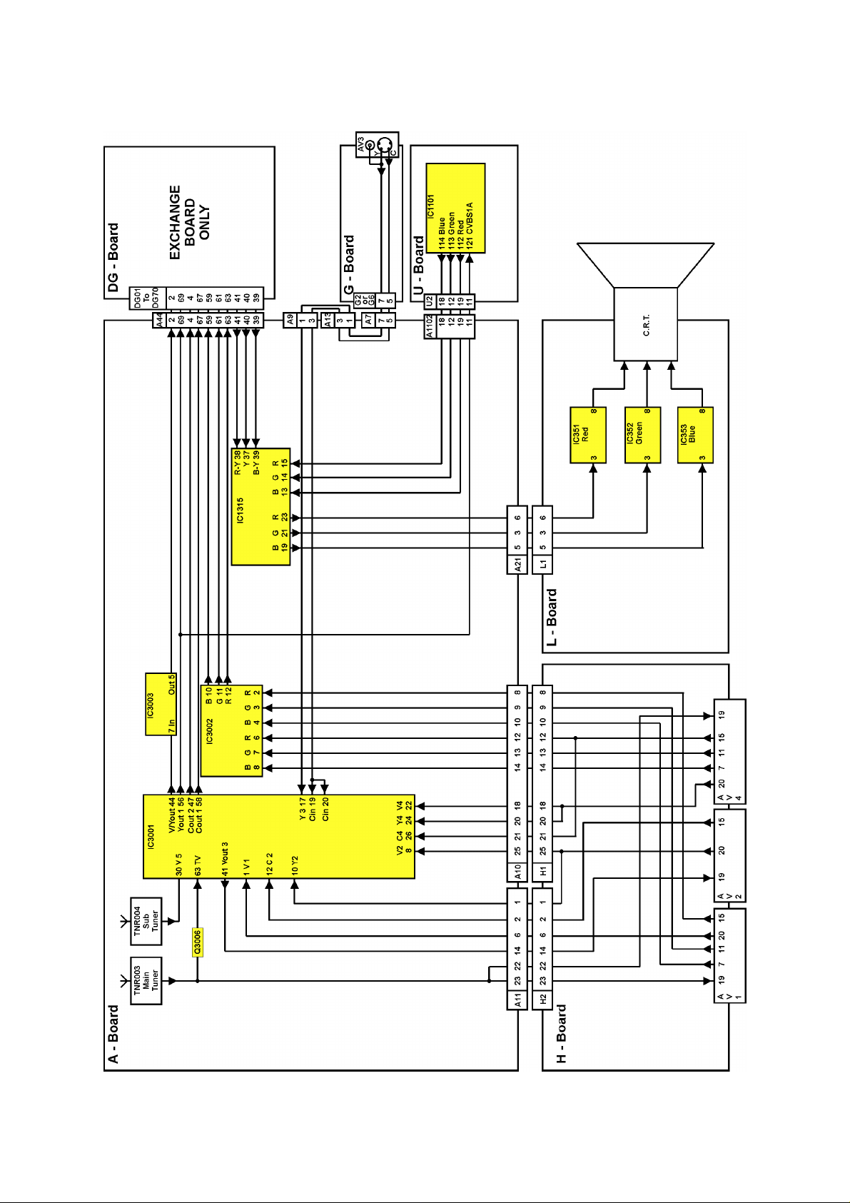
VIDEO BLOCK DIAGRAM
8
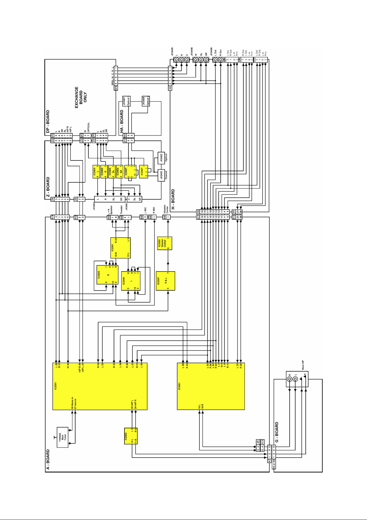
AUDIO BLOCK DIAGRAM
9
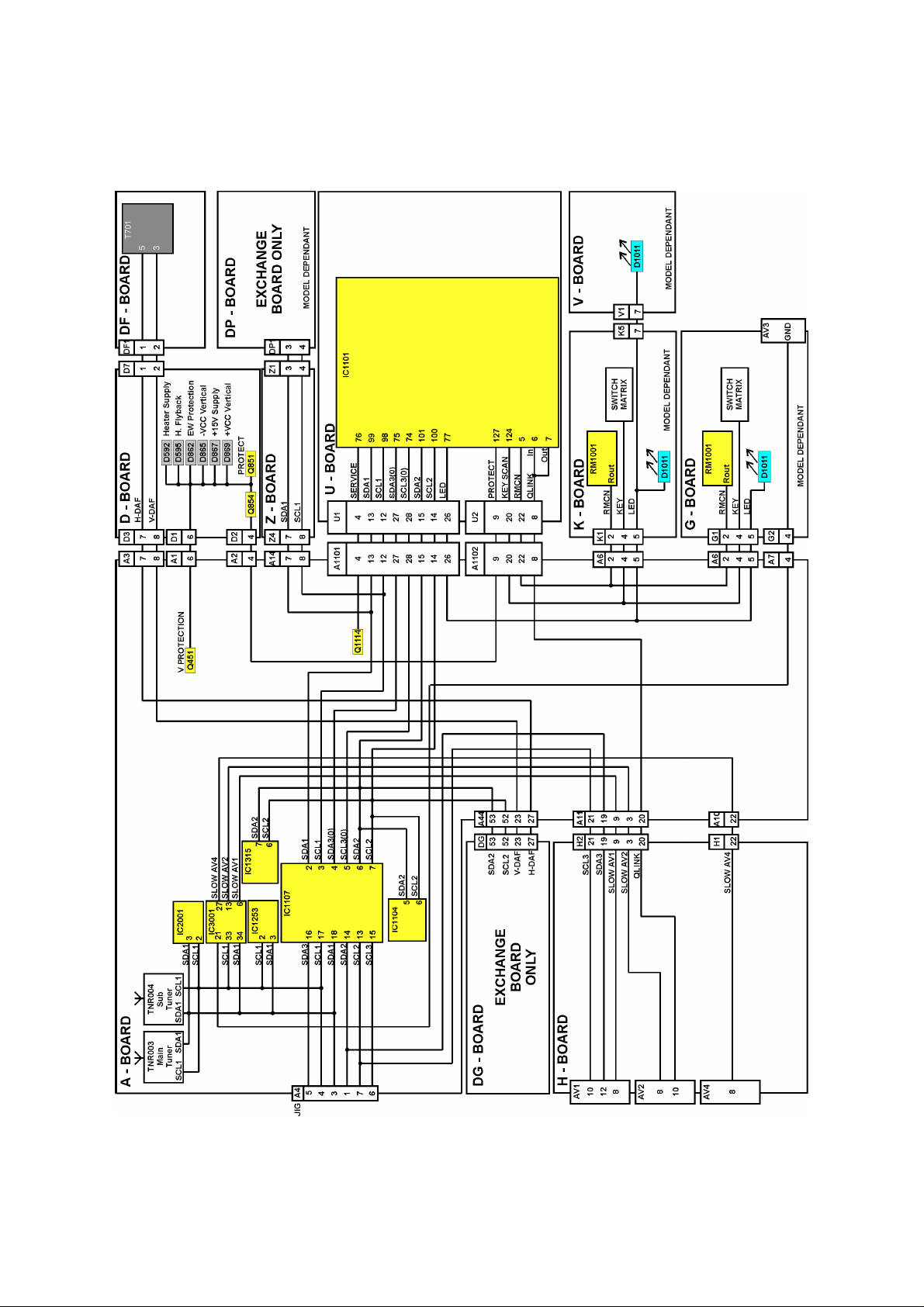
CONTROL BLOCK DIAGRAM
10

POWER SUPPLY BLOCK DIAGRAM
11
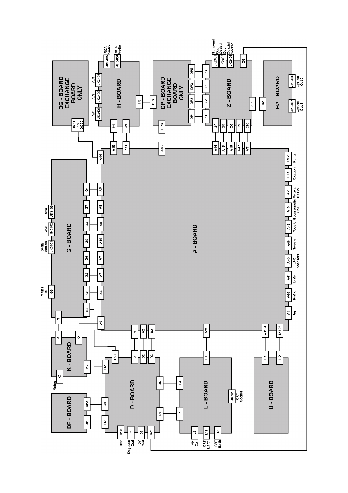
WIRING BLOCK DIAGRAM
12
25
27
4
14
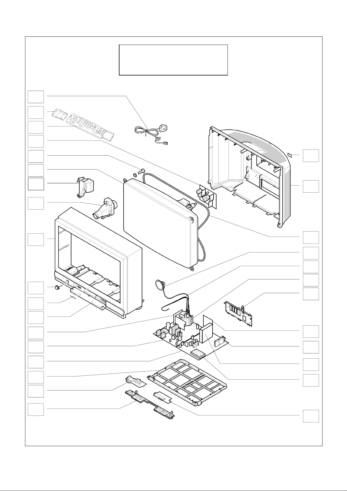
PARTS LOCATION
NOTE:
The numbers on the exploded view below
refer to the mechanical section of the
Replacement Parts List.
7
28
2
1
24
6
5
22
21
23
9
29
26
30
8
17
20
19
11
16
10
12
3
13
18
15
13
Components Identifie d by mark have special charac t eris t ics important for safety.
* When replacing any of these components, us e only manufacturers specified parts.
In case of ordering these spare parts, please always add the c omplete Model-Type
number to your order.
DescriptionCct Ref Parts Number DescriptionCct Ref Parts Number
EXPLODED VIEW
SPEAKER (WOOFER) 1 EAB12149C2
SPEAKER (TWEETER) 2 EASG7DH08B2
TUNER 3 ENG27511G
REMOTE CONTROL 4 EUR511212A
PANASONIC BADGE 5 TBMA060
POWER BUTTON 6 TBXA24302
CRT FIXING SCREW 7 THT1062
AV COVER 8 TKP8E1325
DEGAUSS COIL 9 TLK8E05123
CONTROL BRACKET 10 TMWA003-2
CHASSIS FRAME 11 TMX8E050
H P.C.B. 12 TNPA1724AB
DG P.C.B EXCHANGE UNIT 13 TNPA1725AB
L P.C.B. 14 TNPA1726AF
G P.C.B. 15 TNPA1728AB
K P.C.B. 16 TNPA1729
DF P.C.B. 17 TNPA1806
U P.C.B. 18 TNPA2042AE
A P.C.B. 19 TNPH0348AF
D P.C.B. 20 TNPH0349AC
MODEL LABEL 21 TQF8E3101
DOOR LID 22 TTPA0128
BACK COVER 23 TTUA0370
CABINET 24 TTYA0425-2
POWER CORD 25 TXASX01CJUG
FOCUS LEAD ASSEMBLY 26 TXJF0C0EFG
BATTERY COVER (REMOTE) 27 UR51EC904A
C.R.T. 28 W76EKW10X72
ANODE CABLE 29 ZTBZAD550A
F.B.T. 30 ZTFM77009A
MISCELLANEOUS COMPONENTS
RUBBER FOOT . TBL63413
SET FOOT (REAR) . TBLG3020
AV LABEL . TBM8E2085
LABEL . TBM8E2108
LEFT PRESET LABEL. TBMU101
RIGHT PRESET LABEL. TBMU102
DOOR CATCHER . TEKX008
CRT EARTH SPRING . TES2298
LEFT PANEL . TKPA36805
PANEL RIGHT . TKPA36905
HANDLE . TKRA13110
BACK COVER HANDLE. TKRA19801
GEOMAGNETIC COIL . TLK8E05124
PCB BRACKET . TMW8E042
LED HOLDER . TMWJ019-1
POWER BUTTON JOINT. TMX8E051
CARTON . TPC8E4855
CUSHION TOP . TPD8E743
CUSHION BOTTOM . TPD8E744
CUSHION SUB . TPD8E745
REPLACEMENT PARTS LIST
Important Safety Notice
SERVICE PACK . TZS1EK002
BATTERY PACK . UM-3DJ-2P
VIDEO CABINET . VS-32PG50
INSTRUCTION BOOKS
ENGLISH . TQB8E3140
I.C.s
REGULATOR D354 TL431CLPM
5V REGULATOR IC052 AN7805FLB
RGB OUTPUT IC351 TDA6111Q-N4
RGB OUTPUT IC352 TDA6111Q-N4
RGB OUTPUT IC353 TDA6111Q-N4
VERTICAL OUTPUT IC451 LA7845N
MULTIVIBRATOR IC459 TC74HC221AF
AUDIO AMPLIFIER IC501 NJM2903MTE1
POWER SUPPLY IC801 STRF6656LF53
POWER SUPPLY SWITCHINGIC841 MIP0254SPSCF
ERROR AMPLIFIER IC851 SE140N
MICRO PROCESSOR IC1101 SDA6000-A23
EEPROM * IC1102 E2F0/010/05
EAROM * IC1104 X24BR200-3CA
5V REGULATOR IC1105 S-80843ALY-Z
SDRAM IC1106 TVSA0395
CONVERTER IC1107 TC7MBD3245FK
5V REGULATOR IC1108 AN78L05TA
SYSTEM RESET IC1109 PST9119NR
RESET IC1110 PST9128NR
3.5V REGULATOR IC1251 SI-3033C
2.5V REGULATOR IC1252 PQ30RV21B
D/A CONVERTER IC1253 M62392FP70BC
RESET IC1254 PST9128NR
R.G.B. PROCESSOR IC1315 AN5394FB
M.S.P. IC2001 MSP3410DQAC5
AUDIO AMPLIFIER IC2301 TDA7490
H.P. AMPLIFIER IC2302 AN7108
QUAD AMPLIFIER IC2303 NJM2059MTE1
QUAD AMPLIFIER IC2306 NJM2059MTE1
QUAD AMPLIFIER IC2307 NJM2059MTE1
REGULATOR IC2705 PQ1CG21H2RZ
REGULATOR IC2706 PQ1CG21H2RZ
8V REGULATOR IC2707 AN7808LB
POWER SUPPLY IC2708 SI-8090K
REGULATOR IC2709 PQ1CG21H2RZ
SWITCHING IC3001 CXA2069Q-TL
12V REGULATOR IC3002 TDA8601T/C1
12V REGULATOR IC3302 L78M12MRB
OPERATIONAL AMPLIFIER IC4801 AN6564NS-E1
GEOMAGNETIC CORRECTIONIC4802 PUB4301
LED RECEIVER RM1001 RPM6937-S
FUSES
FUSE HOLDER F801-1 EYF52BC
FUSE HOLDER F801-2 EYF52BC
FUSE F801 XBA2C50TH15
14

DIODES
DescriptionCct Ref Parts Number DescriptionCct Ref Parts Number
DIODE D003 MA3150HTX
DIODE D004 MA3150HTX
DIODE D010 MA152KTX
DIODE D351 ERA15-04V3
DIODE D352 ERA15-04V3
DIODE D353 MA3110LTX
DIODE D355 ERA15-04V3
DIODE D356 ERA15-04V3
DIODE D358 MA151ATX
DIODE D360 ERA15-02V3
DIODE D361 MA151ATX
DIODE D362 MA151ATX
DIODE D363 MA151ATX
DIODE D364 MA3130MTX
DIODE D365 MA3130MTX
DIODE D366 MA3130MTX
DIODE D367 MA3051HTX
DIODE D368 MA3051HTX
DIODE D369 MA3051HTX
DIODE D383 ERA15-04V3
DIODE D385 ERA22-04V3
DIODE D386 ERA15-04V3
DIODE D389 ERA15-04V3
DIODE D452 MA152KTX
DIODE D453 EU02AV1
DIODE D454 MA152KTX
DIODE D455 MA152KTX
DIODE D456 ERA22-02V3
DIODE D465 MA3039HTX
DIODE D502 MA4150TA
DIODE D503 ERA81004V3
DIODE D504 D1NL40V70
DIODE D521 AU02AV0
DIODE D522 AU02AV0
DIODE D523 MA165TA5
DIODE D524 MA165TA5
DIODE D525 RP1HLFA5
DIODE D526 RP1HLFA5
DIODE D553 MA167TA5
DIODE D554 EU02
DIODE D555 RH3GLF102
DIODE D557 MA1033MTA
DIODE D558 AU02V0
DIODE D559 FMV-3GULF730
DIODE D560 MA165TA5
DIODE D562 MA182TA
DIODE D570 RU3ANV1
DIODE D580 MA4360
DIODE D591 MA165TA5
DIODE D592 MA4104
DIODE D593 ERA15-02V3
DIODE D594 MA165TA5
DIODE D595 MA4360MTA
DIODE D701 D1NL40V70
DIODE D802 D6SB80LF-B
DIODE D805 MA2240-BLFS
DIODE D809 MA2082-ALFS
DIODE D811 MA2082-ALFS
DIODE D819 ERA22-04V3
DIODE D820 ERA22-04V3
DIODE D821 ERA22-04V3
DIODE D823 PC123FY2
THERMISTOR D825 232266296706
THERMISTOR D826 232266296706
DIODE D843 ERC0510V1
TRA NSIST OR S
DIODE D844 TVSSR2KL
DIODE D845 RY24V1
DIODE D847 ERA22-10
DIODE D848 PC123FY2
DIODE D851 FMGG26S
DIODE D852 MA4030LTA
DIODE D853 RU2AMLFA1
DIODE D854 RU2AMLFA1
DIODE D855 FMGG2CS
DIODE D856 EU02
DIODE D857 FMGG26S
DIODE D858 MA165TA5
DIODE D859 MA165TA5
DIODE D861 MA165TA5
DIODE D862 MA4360MTA
DIODE D865 MA165TA5
DIODE D867 MA165TA5
DIODE D869 MA165TA5
DIODE D881 MA165TA5
DIODE D885 MA4056HTA
DIODE D886 MA165TA5
DIODE D887 MA165TA5
DIODE D888 EU02
DIODE D953 R2KNLFA1
DIODE D961 MA152KTX
L.E.D. D1011 LNH201RFCC4
DIODE D1152 MA152KTX
DIODE D1153 MA152KTX
DIODE D1302 MA152KTX
DIODE D1306 MA3062MTX
DIODE D1307 MA3091MTX
DIODE D1308 MA152KTX
DIODE D1309 MA152KTX
DIODE D1310 MA3062MTX
DIODE D1311 MA3062MTX
DIODE D1312 MA3062MTX
DIODE D1313 MA3043MTX
DIODE D1315 MA3043MTX
DIODE D2040 MA152KTX
DIODE D2041 MA152KTX
DIODE D2048 MA152KTX
DIODE D2301 TVSRM26V1
DIODE D2302 MTZJT-775.6B
DIODE D2305 MA3047MTX
DIODE D2306 MA29TA5
DIODE D2311 MA1180HTA
DIODE D2312 MA3130MTX
DIODE D2313 MA152KTX
DIODE D2314 MA152KTX
DIODE D2316 MA152KTX
DIODE D2711 RK34LFC4
DIODE D2712 AK04V0
DIODE D2713 RK34LFC4
DIODE D2714 RK34LFC4
DIODE D3003 MA3091LTX
DIODE D3004 MA3091LTX
DIODE D3103 MA165TA5
DIODE D3104 MA165TA5
DIODE D3401 MA165TA5
DIODE D3402 MA165TA5
TRANSISTOR Q002 BC857B
TRANSISTOR Q369 BC857B
TRANSISTOR Q451 BC847B
TRANSISTOR Q460 BC847B
TRANSISTOR Q461 BC847B
15
 Loading...