

Panasonic TX-32LXD50, TX-26LXD50, TX-32LX50F, TX-32LX50P, TX-26LX50F Service manual
...
TX-32LXD50
A
A
A
A
A
r
/
TX-26LXD50
TX-32LX50F
TX-32LX50P
TX-26LX50F
TX-26LX50P
LH41 Chassis
ORDERNO.PCZ0503030C2
Wide LCD TV
Specifications
PowerSource
PowerConsumption
LCD Wide XGA (1,366 × 768 pixels)
Screen Size 575.8 mm (W) × 323.7 mm (H) (TX-26LXD50, TX-26LX50F/P)
Sound
Speake
Audio Output 20 W (5.4 W + 5.4 W, 4.6 W + 4.6 W )
Headphones M3 (3.5 mm) Jack × 1
Scanning format 480i(60Hz), 480p(60Hz), 576i(50Hz), 576p(50Hz), 720p(50Hz), 1080i(50Hz)
Receiving Systems
Band name DVB (TX-26LXD50/32LXD50) Digital terrestrial services via UHF aerial input.
C 220 - 240 V, 50/60 Hz
verage use : 133 W (0.78 A) (TX-26LXD50)
verage use : 169 W (0.98 A) (TX-32LXD50)
Standbycondition :
0.1 W (Witho ut DVB Timerprogrammes)
11W (With DVB Timerprogrammes)
verage use : 126 W (TX-26LX50F/P)
verage use : 161 W (TX-32LX50F/P)
Standbycondition : 0.4 W
16 : 9 aspect ratio LCD panel
697.7 mm (W) × 392.3 mm (H) (TX-32LXD50,TX-32LX50F/P)
WooferØ8 cm × 2 pcs, Full range Ø5 cm ×2pcs
PAL I (TX-26LXD50/32LXD50) UHF E21-68.
PAL B, G, H, SECAM B, G SECAML/L’ (TX-26LX50F/P, TX-32LX50F/P)
VHF E2 - E12 VHF H1 - H2 (ITALY)
VHF A - H (ITALY) UHF E21 - E69
CATV (S01 - S05) CATV S1 - S10 (M1 - M10)
© 2005 Matsushita Electric Industrial Co., Ltd. All
rights reserved. Unauthorized copying and
distribution is a violation of law.
r
V
V
TX-32LXD50 / TX-26LXD50 / TX-32LX50F / TX-32LX50P / TX-26LX50F / TX-26LX50P
CATV S11 - S20 (U1 - U10) CATV S21 - S41 (Hyperband)
PAL D, K, SECAMD,K(TX-26LX50F/P, TX-32LX50F/P)
VHF R1 - R2 VHF R3 - R5
VHF R6 - R12 UHF E21 - E69
PAL 525/60 Playback of NTSC tape from some PAL Video re cord
M.NTSC Playback from M. NTSC Video recorders (VCR)
NTSC (AVinput only) Playback from NTSC Video recorders (VCR)
Aerial - Rea
Operating Conditions Temperature:5°C-35°C
Connection Terminals
AV1 (Scart connecter) 21 Pin terminal (Audio/Video in, Audio/Video out, RGB in)
AV2 (Scart connecter) 21 Pin terminal (Audio/Video in, Audio/Video out, S-Video in, Q-Link)
AV3
IDEO RCA PIN Type × 1
S-VIDEO Mini DIN 4-pin
AUDIO L - R RCA PIN Type × 2
AV4(Scart connecter) 21 Pin terminal (Audio/Video in, Audio/Video out, RGB in, S-Video in, Q-Link)
COMPONENT
IDEO Y, P B, PR
AUDIO L - R RCA PIN Type × 2
Output
AUDIO L - R RCA PIN Type × 2
Dimensions ( W × H × D )
Including TV Stand 663 mm × 556 mm × 299.5 mm (TX-26LXD50, TX-26LX50F/P)
TV Set Only 663 mm × 494.3 mm × 140.7 mm (TX-26LXD50, TX-26LX50F/P)
Mass (Weight) 18 kg Net (TX-26LXD50, TX-26LX50F/P)
UHF (TX-26/32LXD50) UHF/VHF (TX-26/32LX50F/P)
Humidity: 5 % - 90 % RH (non-condensing)
795 mm × 634.7 mm × 299.5 mm (TX-32LXD50, TX-32LX50F/P)
795 mm × 573 mm × 140.7 mm (TX-32LXD50, TX-32LX50F/P)
21 kg Net (TX-32LXD50, TX-32LX50F/P)
ers (VCR)
CONTENTS
Page Page
1 Safety Precautions 4
1.1. General Guidelines
1.2. Touch-Current Check
2 Prevention of Electro Static Discharge (ESD) to
Electrostatically Sensitive (ES) Devices
3 Applicable signals
4 Self Check Function
4.1. Self Check
4.2. Power LED Blinking timing chart
5 Chassis Board Layout
6 Before servicing
6.1. Kind and location of the flexible cable and bridge cable
6.2. How to remove the connector
6.3. Wire dressing 1
4
4
5
5
6
6
7
8
9
9
10
11
6.4. Wire dressing 2
7 Servicing method
7.1. Removing the stand assエy
7.2. Removing the rear cover
7.3. Removing the speaker box L and R
7.4. Removing the rear AV bracket
7.5. Removing the rear metal frame
7.6. Removing the P-Board
7.7. Removing the XV-Board (For LXD50 model only)
7.8. Removing the DG-Board
7.9. Removing the AP-Board
7.10. Removing the H-Board
7.11. Removing G-Board bracket
7.12. Removing the G-Board
2
12
13
13
13
13
14
14
14
14
15
15
15
15
16
TX-32LXD50 / TX-26LXD50 / TX-32LX50F / TX-32LX50P / TX-26LX50F / TX-26LX50P
7.13. Removing the K-Board 16
7.14. Removing the V-Board
7.15. Removing the main chassis
7.16. Removing the LCD panel
8 Service Mode Function
8.1. How to enter SERVICE 1
8.2. How to enter SERVICE 2
8.3. Option Description
8.4. Option Code Setting
9 Adjustment method
9.1. White Balance Adjustment
10 Block Diagram
10.1. Signal (1/3) Block Diagram
10.2. Signal (2/3) Block Diagram
10.3. Signal (3/3) Block Diagram
10.4. Power (1/3) Block Diagram
10.5. Power (2/3) Block Diagram
10.6. Power (3/3) Block Diagram
11 Schematic Diagram
11.1. Schematic Diagram Notes
11.2. AP-Board (1/2) and K-Board Schematic Diagram
11.3. AP-Board (2/2) Schematic Diagram
11.4. XV-Board (1/5) Schematic Diagram
11.5. XV-Board (2/5) Schematic Diagram
11.6. XV-Board (3/5) Schematic Diagram
11.7. XV-Board (4/5) Schematic Diagram
11.8. XV-Board (5/5) Schematic Diagram
11.9. H-Board (1/3) Schematic DIagram
16
16
17
18
18
18
21
23
24
24
25
25
26
27
28
29
30
31
31
32
33
34
35
36
37
11.10. H-Boa rd (2/3) Schematic Diagram
11.11. H-Boa rd (3/3) Schematic Diagram
11.12. DG-B oard (1/6) Schematic Diagram
11.13. DG-B oard (2/6) Schematic Diagram
11.14. DG-B oard (3/6) Schematic Diagram
11.15. DG-B oard (4/6) Schematic Diagram
11.16. DG-B oard (5/6) Schematic Diagram
11.17. DG-B oard (6/6) Schematic Diagram
11.18. G-Boa rd and V-Board Schematic Diagram
12 Printed Circuit Board
12.1. AP-Board
12.2. XV-Board (TX-26/32LXD50 only)
12.3. H-Board
12.4. DG-Board
12.5. G-Board
12.6. K-Board and V-Board
13 Exploded View and Replacement Parts List.
13.1. Set Layout
13.2. Front Chassis Layout
13.3. Packing Exploded View
13.4. Mechanical Replacement Parts List
14 Electrical Replacement Parts List
14.1. Electrical Replacement Parts List Notes
14.2. Electrical Replacement Parts List (TX-32/26LXD50)
14.3. Electrical Replacement Parts List (TX-32/26LX50F/P)
38
39
40
41
42
43
44
45
46
47
48
49
49
51
53
56
59
60
61
61
62
63
64
66
66
67
85
3
TX-32LXD50 / TX-26LXD50 / TX-32LX50F / TX-32LX50P / TX-26LX50F / TX-26LX50P
1 Safety Precautions
1.1. General Guidelines
1. When servicing, observe the original lead dress. If a short circuit is found, replace all parts which have been overheated or
damaged by the short circuit.
2. After servicing, see to it that all the protective devices such as insulation barriers, insulation papers shields are properly
installed.
3. After servicing, make the following leakage current checks to prevent the customer from being exposed to shock hazards.
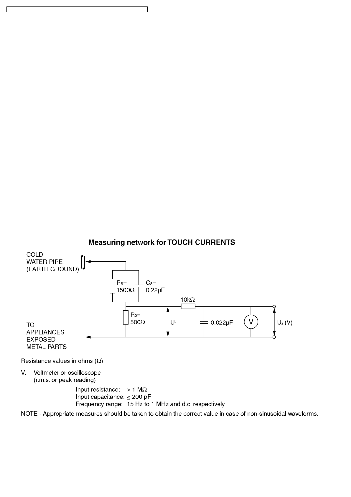
1.2. Touch-Current Check
1. Plug the AC cord directly into the AC outlet. Do not use an isolation transformer for this check.
2. Connect a measuring network for touch currents between each exposed metallic part on the set and a good earth ground such
as a water pipe, as shown in Figure 1.
3. Use Leakage Current Tester (Simpson 228 or equivalent) to measure the potential across the measuring network.
4. Check each exposed metallic part, and measure the voltage at each point.
5. Reserve the AC plug in the AC outlet and repeat each of the above measure.
6. The potential at any point (TOUGH CURRENT) expressed as voltage U
For a. c.: U
For d. c.: U
= 35 V (peak) and U2= 0.35 V (peak);
1
= 1.0 V,
1
Note:
The limit value of U
= 0.35 V (peak) for a. c. and U1= 1.0 V for d. c. correspond to the values 0.7 mA (peak) a. c. and 2.0
2
mA d. c.
The limit value U
= 35 V (peak) for a. c. correspond to the value 70 mA (peak) a. c. for frequencies greater than 100 kHz.
1
7. In case a measurement is out of the limits specified, there is a possibility of a shock hazard, and the equipment should be
repaired and rechecked before it is returned to the customer.
and U2, does not exceed the following values:
1
Figure 1
4
TX-32LXD50 / TX-26LXD50 / TX-32LX50F / TX-32LX50P / TX-26LX50F / TX-26LX50P
2 Prevention of Electro Static Discharge (ESD) to
Electrostatically Sensitive (ES) Devices
Some semiconductor (solid state) devices can be damaged easily by static electricity. Such components commonly are called
Electrostatically Sensitive (ES) Devices. Examples of typical ES devices are integrated circuits and some field-effect transistors and
semiconductor "chip" components. The following techniques should be used to help reduce the incidence of component damage
caused by electro static discharge (ESD).
1. Immediately before handling any semiconductor component or semiconductor-equipped assembly, drain off any ESD on your
body by touching a known earth ground. Alternatively, obtain and wear a commercially available discharging ESD wrist strap,
which should be removed for potential shock reasons prior to applying power to the unit under test.
2. After removing an electrical assembly equipped with ES devices, place the assembly on a conductive surface such as alminum
foil, to prevent electrostatic charge buildup or exposure of the assembly.
3. Use only a grounded-tip soldering iron to solder or unsolder ES devices.
4. Use only an anti-static solder removal device. Some solder removal devices not classified as "anti-static (ESD protected)" can
generate electrical charge sufficient to damage ES devices.
5. Do not use freon-propelled chemicals. These can generate electrical charges sufficient to damage ES devices.
6. Do not remove a replacement ES device from its protective package until immediately before you are ready to install it. (Most
replacement ES devices are packaged with leads electrically shorted together by conductive foam, alminum foil or comparable
conductive material).
7. Immediately before removing the protective material from the leads of a replacement ES device, touch the protective material
to the chassis or circuit assembly into which the device will be installed.
Caution
Be sure no power is applied to the chassis or circuit, and observe all other safety precautions.
8. Minimize bodily motions when handling unpackaged replacement ES devices. (Otherwise hamless motion such as the brushing
together of your clothes fabric or the lifting of your foot from a carpeted floor can generate static electricity (ESD) sufficient to
damage an ES device).
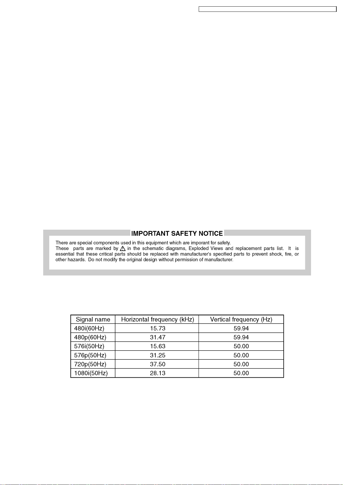
3 Applicable signals
Applicable input signal for Component (Y, PB,PR)
Note:
Signals without above specification may not be displayed properly.
5
TX-32LXD50 / TX-26LXD50 / TX-32LX50F / TX-32LX50P / TX-26LX50F / TX-26LX50P
4 Self Check Function
4.1. Self Check
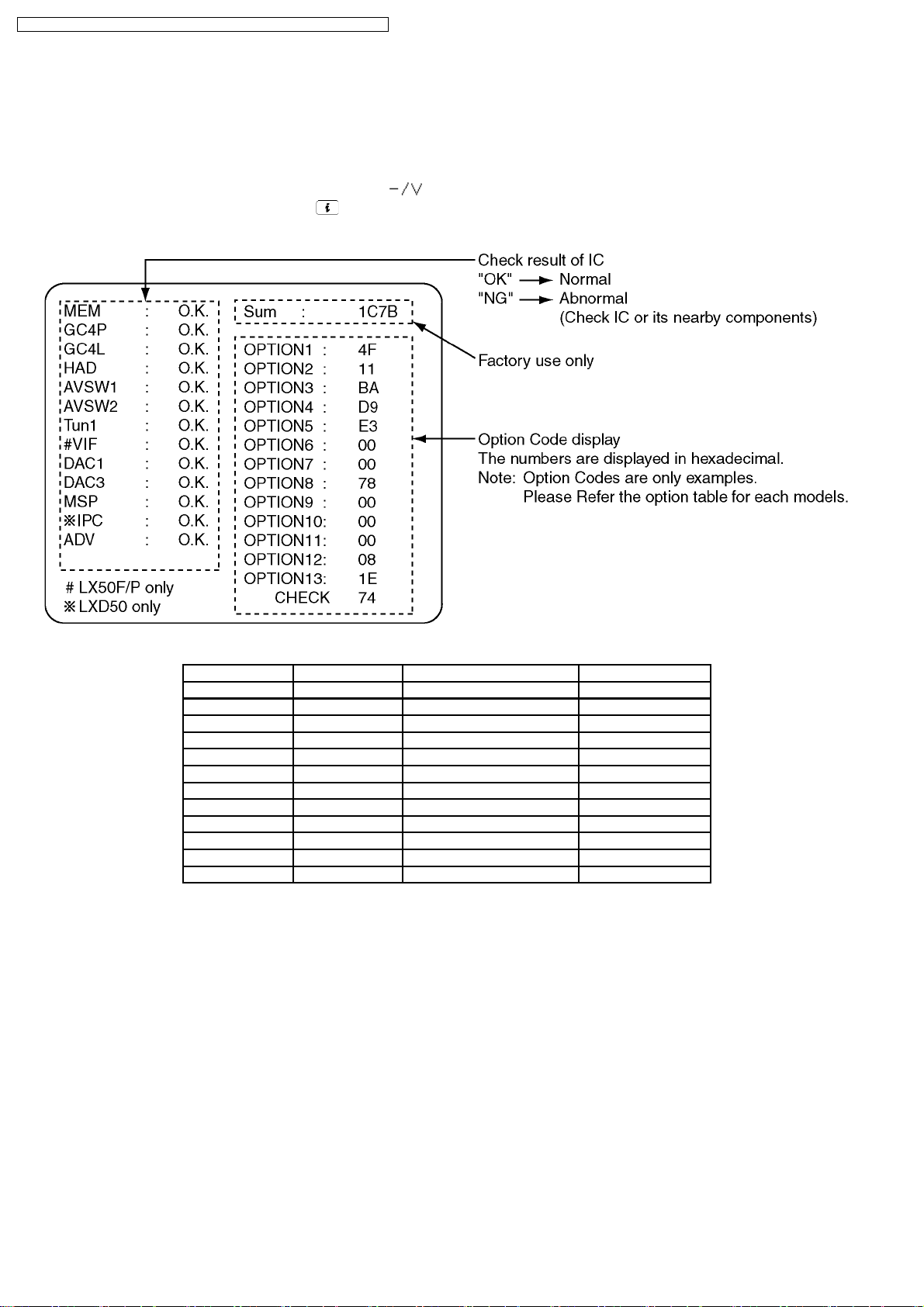
1. Self-Check is used to automatically check the bus lines and hexadecimal code of the TV set.
2. To get into the Self -Check mode press the Down (
time pressing the Status/Information (
) button on the remote control, and the screen will show :
3. Turn off the TV to reset JPEG Viewer circuit after SELF-CHECK.
) button on the customer controls at the front of the set, at the same
If the CCU ports have been checked and found to be incorrect or not located then “--” will appear in place of “O.K.”.
Display Ref. No. Description P.C.B.
MEM IC1107 Memory DG-Board
GC4P IC4054 Global Core DG-Board
GC4L IC4057 Global Core DG-Board
HAD IC4012 OSD RGB A/D Converter DG-Board
AVSW1 IC3005 AV Switch VIDEO H-Board
AVSW2 IC2105 AV Switch AUDIO H-Board
Tun1 TU3201 Tuner H-Board
DAC1 IC1106 DAC control 1 DG-Board
DAC3 IC3006 DAC control 3 H-Board
MSP IC2106 Stereo Decoder H-Board
IPC IC8013 HDSL PEAKS Lite XV-Board
ADV IC4005 A/D Converter DG-Board
6
TX-32LXD50 / TX-26LXD50 / TX-32LX50F / TX-32LX50P / TX-26LX50F / TX-26LX50P
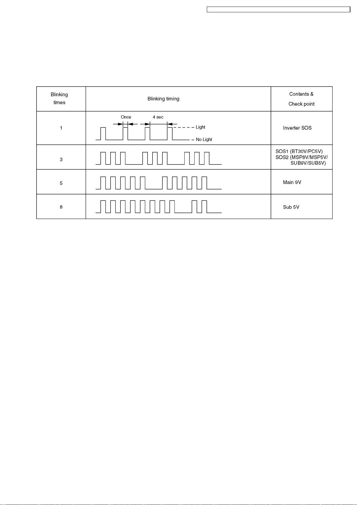
4.2. Power LED Blinking timing chart
1. Subject
Information of LED Flashing timing chart.
2. Contents
When an abonormality has occurred the unit, the protection circuit operates and reset to the stand by mode. At this time, the
defective block can be identified by the number of blinking of the Power LED on the front panel of the unit.
7
TX-32LXD50 / TX-26LXD50 / TX-32LX50F / TX-32LX50P / TX-26LX50F / TX-26LX50P
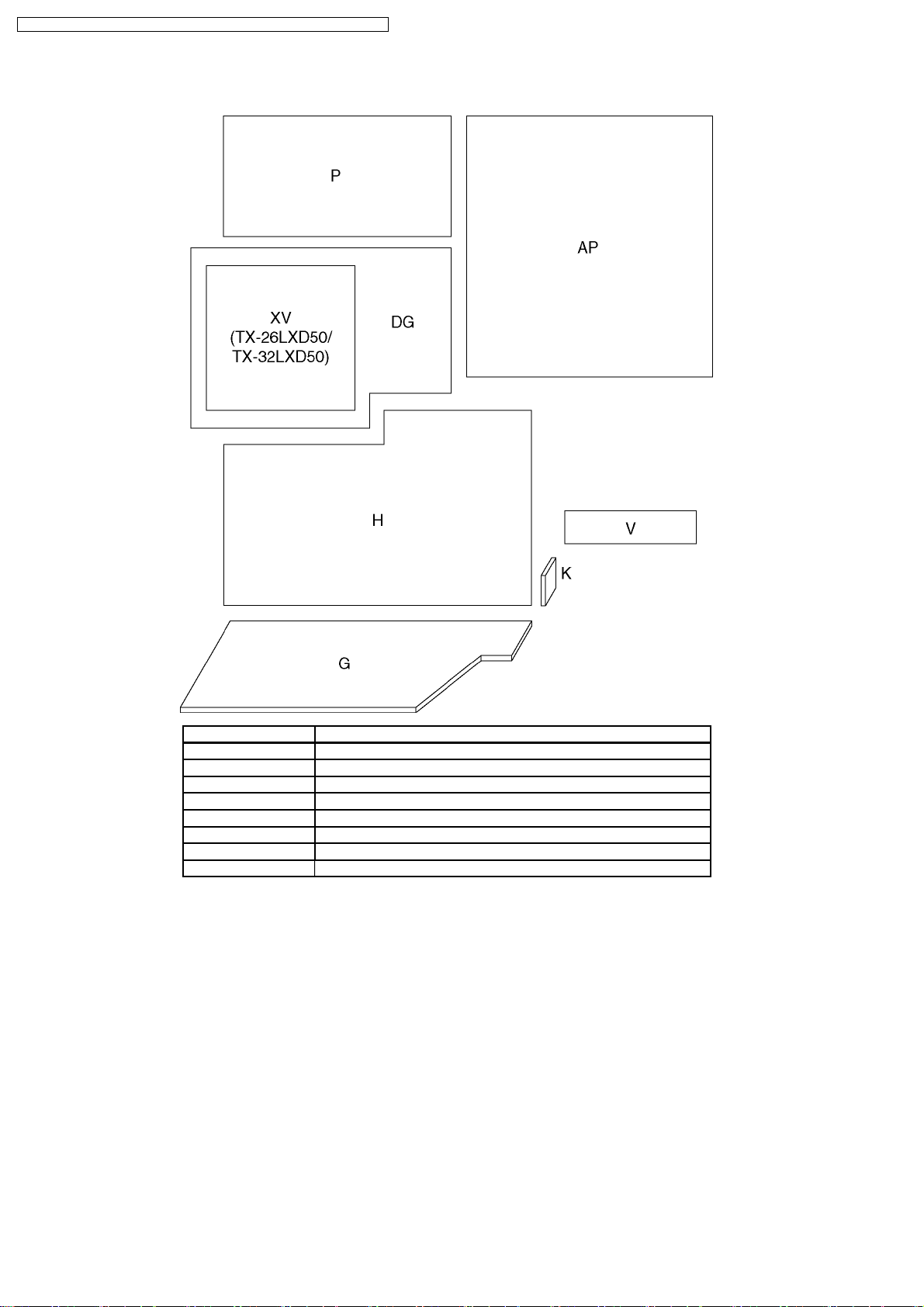
5 Chassis Board Layout
Board Name Function
AP-Board Regulator
DG-Board Global Core, A/D Converter, MCU
H-Board AV connector, TV Tuner, AV Switch
K-Board Power Switch
G-Board Front AV & HP connector, Key Switch
P-Board DC Power Supply
V-Board Remote Receiver, LED
XV-Board DVB Tuner
8
TX-32LXD50 / TX-26LXD50 / TX-32LX50F / TX-32LX50P / TX-26LX50F / TX-26LX50P
6 Before servicing
6.1. Kind and location of the flexible cable and bridge cable
Ref No. Connecter type Pins Location Opposite Ref No.
G1 - 10pin G-Board V1
G4 - 30pin G-Board H4
G5 - 20pin G-Board H5
G10 - 4pin G-Board speaker box L
G11 - 5pin G-Board speaker box R
AP1 Bridge Type 23pin AP-Board H1
AP2 - 7pin AP-Board P5 (CN101)
AP3 Bridge Type 11pin AP-Board P3
AP4 Bridge Type 22pin AP-Board DG4
AP5 Bridge Type 22pin AP-Board DG5
AP6 - 3pin AP-Board K6
DG3 Flexible type 40pin DG-Board H3
DG4 Bridge type 23pin DG-Board AP4
DG5 Bridge type 23pin DG-Board AP5
DG6 - 8pin DG-Board LCD Panel
DG7 - 32pin DG-Board LCD Panel
H1 Bridge type 23pin H-Board AP1
H4 - 30pin H-Board G4
H5 - 20pin H-Board G5
H3 Flexible type 40pin H-Board DG3
AP10 - 2pin AP-Board AC cord
K6 - 3pin K-Board AP6
P1 (CN203) - 8pin P-Board CN1 (Inverter)
P2 (CN101) - 7pin P-Board AP2
P3 (CN201) Bridge Type 11pin P-Board AP3
V1 - 10pin V-Board G1
9
TX-32LXD50 / TX-26LXD50 / TX-32LX50F / TX-32LX50P / TX-26LX50F / TX-26LX50P
6.2. How to remove the connector
Bridge cable connector
Flexible cable connector
10
TX-32LXD50 / TX-26LXD50 / TX-32LX50F / TX-32LX50P / TX-26LX50F / TX-26LX50P
6.3. Wire dressing 1
1. Put a ferrite core (JOKF00000018) to the AP6-K6 (Power Switch) connecting wire as illustrated below.
2. Put a ferrite core (JOKG00000054) to the power cord as illustrated below.
3. Make the wire dressing as illustrated below.
11
TX-32LXD50 / TX-26LXD50 / TX-32LX50F / TX-32LX50P / TX-26LX50F / TX-26LX50P
6.4. Wire dressing 2
<Clamping>
Notes :
1. Connect every connector surely.
2. Manage wires not to touch any sharp edge of the metal parts.
3. Manage wires not to have too much tension.
:for 32 inch model only.
4.
12
7 Servicing method
TX-32LXD50 / TX-26LXD50 / TX-32LX50F / TX-32LX50P / TX-26LX50F / TX-26LX50P
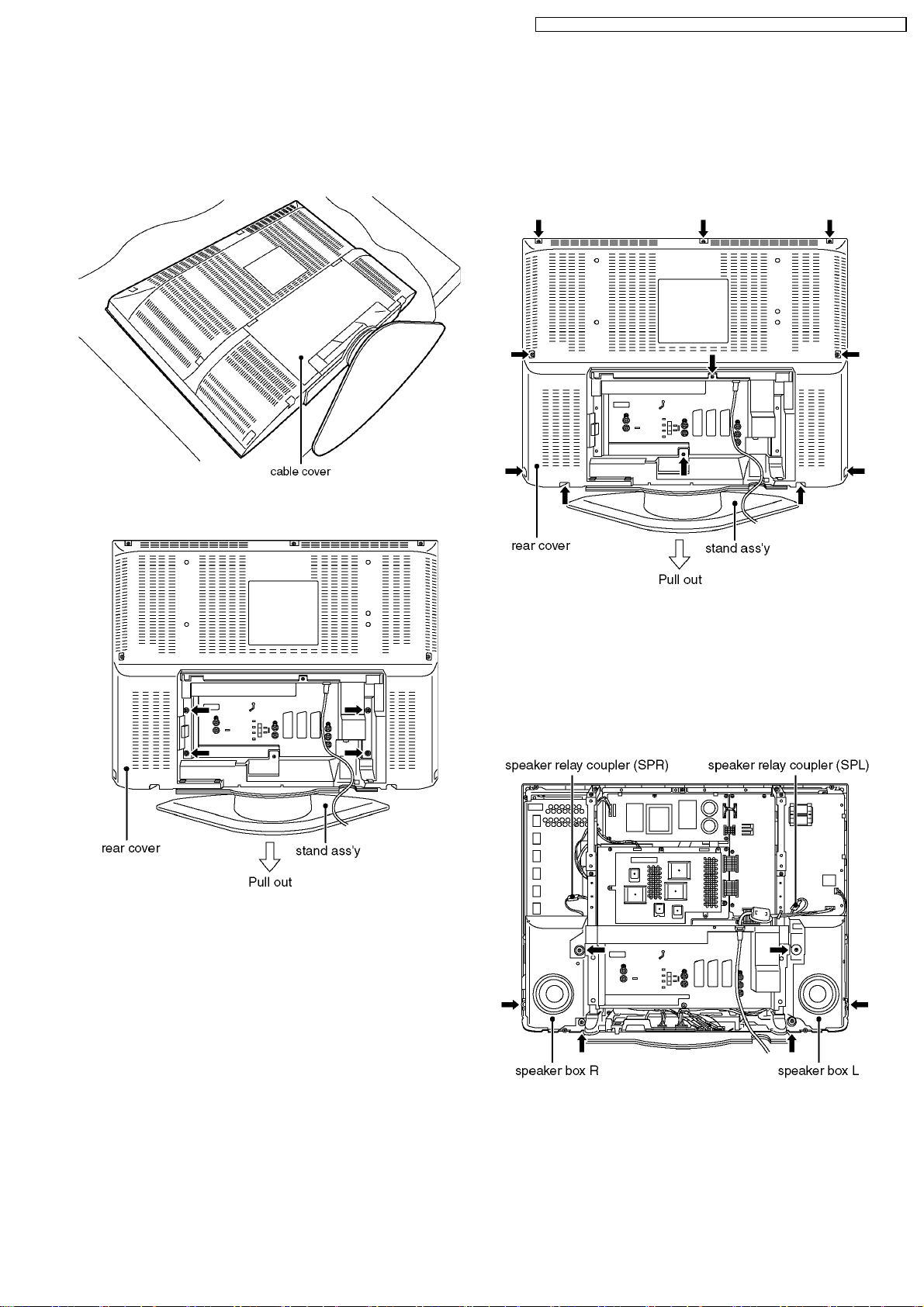
7.1. Removing the stand ass´y
1. Lay down the main unit so that the rear cover faces upward.
2. Remove the cable cover.
3. Remove the fixing screws (4pcs).
4. Remove the stand ass´y.
7.2. Removing the rear cover
1. Remove the stand ass´y. (See 7.1.)
2. Remove the fixing screws (11pcs).
3. Remove the rear cover.
7.3. Removing the speaker box L
and R
1. Remove the rear cover. (See 7.2.)
2. Disconnect the speaker relay couplers (SPL and SPR).
3. Remove the fixing screws (6pcs).
4. Remove the speaker box L and R.
13
TX-32LXD50 / TX-26LXD50 / TX-32LX50F / TX-32LX50P / TX-26LX50F / TX-26LX50P
7.4. Removing the rear AV bracket
1. Remove the rear cover (See 7.2.) and the speaker box L
and R. (See 7.3.)
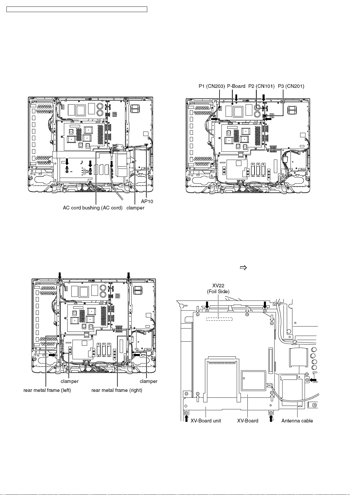
2. Release the AC cord from the rear AV bracket and clamper
on the rear metal frame, and remove the AC cord. (the
coupler AP10)
3. Remove the fixing screws (3pcs).
4. Remove the rear AV bracket ass´y.
7.6. Removing the P-Board
1. Remove the rear cover. (See 7.2.)
2. Disconnect the couplers P2 (CN101), P3 (CN201) and P1
(CN203).
3. Remove the fixing screw (4pcs).
4. Remove the P-Board.
7.5. Removing the rear metal frame
1. Remove the rear AV bracket. (See 7.4.)
2. Release the cables from the clampers on the rear metal
frames.
3. Remove the fixing screws (4pcs).
4. Remove the rear metal frames (right and left).
7.7. Removing the XV-Board (For
LXD50 model only)
1. Remove the rear AV bracket (See 7.4.) and the rear metal
frame. (See 7.5.)
2. Disconnect the couplers carefully (XV22 and DG22).
3. Remove the fixing screws (5pcs).
4. Remove the XV-Board unit.
5. Remove the screws (×5
6. Remove the XV-Board.
)
14
TX-32LXD50 / TX-26LXD50 / TX-32LX50F / TX-32LX50P / TX-26LX50F / TX-26LX50P
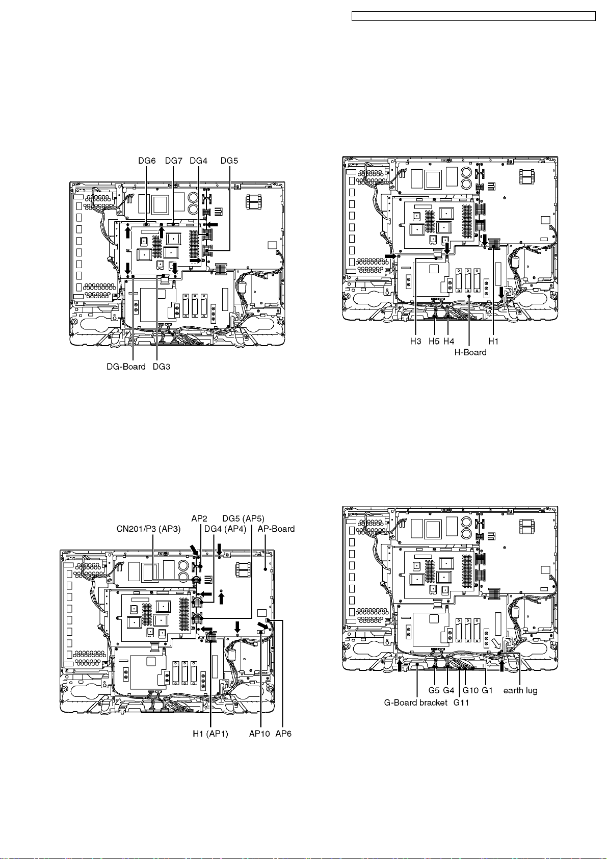
7.8. Removing the DG-Board
1. Remove the rear AV bracket (See 7.4.) and the rear metal
frame. (See 7.5.)
2. Disconnect the couplers (DG6 and DG7), the flexible cable
(DG3) and the bridge cables (DG4 and DG5).
3. Remove the fixing screws (6pcs).
4. Remove the DG-Board.
7.10. Removing the H-Board
1. Remove the rear AV bracket (See 7.4.) (and the rear metal
frame). (See 7.5.)
2. Disconnect the flexible cable (H3), the bridge cable (H1)
and the couplers (H4 and H5).
3. Remove the fixing screws (4pcs).
4. Remove the H-Board.
7.9. Removing the AP-Board
1. Remove the rear AV bracket ass´y (See 6.4.) and the rear
metal frame. (See 6.5.)
2. Disconnect the couplers (AP2, AP6 and AP10 (AC Cord))
and the bridge cables (H1 (AP1) on the H-Board, P3/CN201
(AP3) on the P-Board and DG4 (AP4) and DG5 (AP5) on
the DG-Board.
3. Remove the fixing screws (7pcs).
4. Remove the AP-Board.
7.11. Removing G-Board bracket
1. Remove the rear AV bracket (See 7.4.).
2. Disconnect the couplers (G1, G4, G5, G10 and G11).
3. Remove a screw on the DG-Board and release the earth
lug from the G-Board.
4. Release the cables from the cable holders of the G-Board
bracket.
5. Remove the fixing screws (2pcs).
6. Remove the G-Board bracket (with the G-Board).
15
TX-32LXD50 / TX-26LXD50 / TX-32LX50F / TX-32LX50P / TX-26LX50F / TX-26LX50P
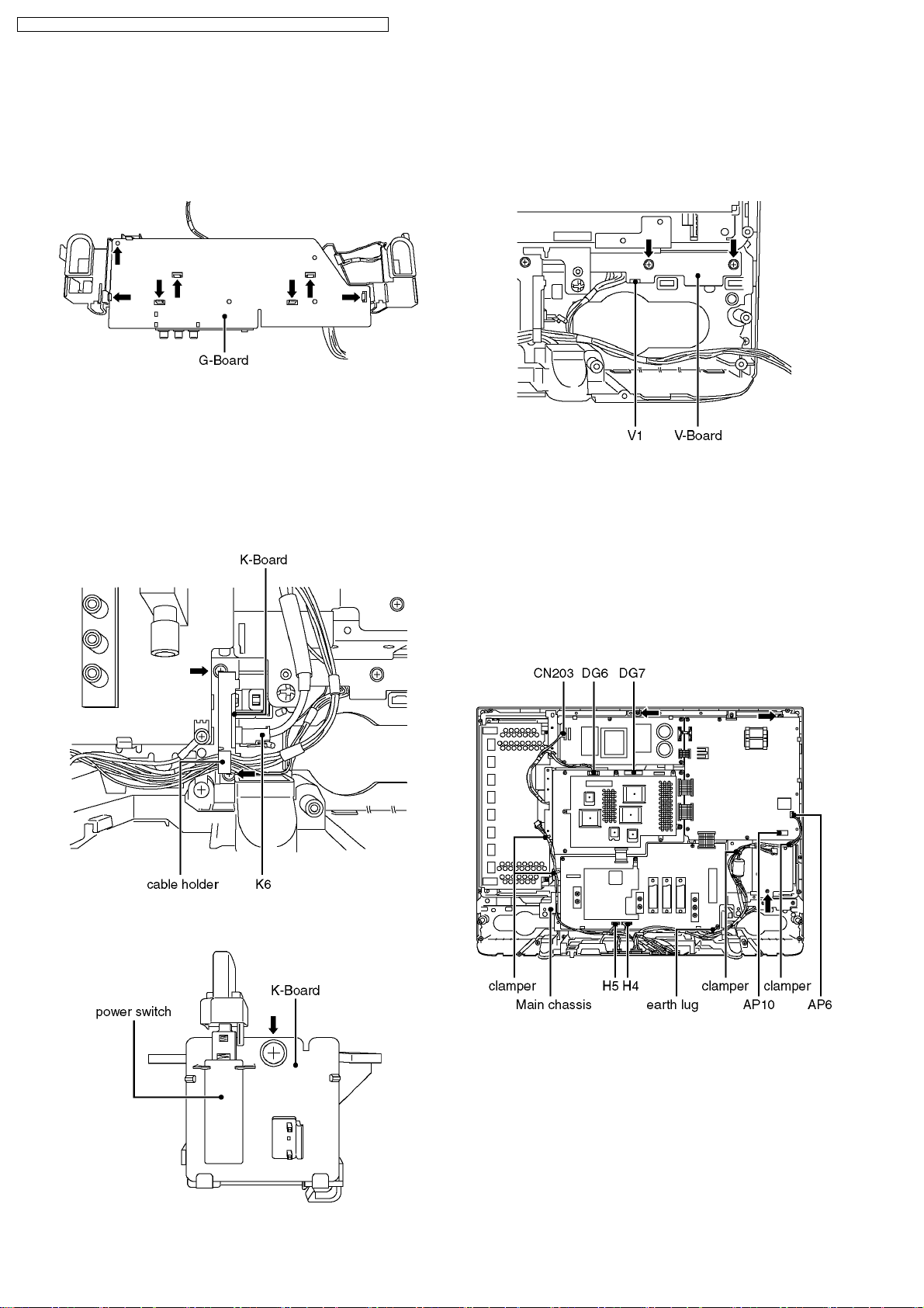
7.12. Removing the G-Board
1. Remove the G-Board bracket. (See 7.10.)
2. Push the hooks (7 points) to release the G-Board from the
G-Board brackets.
3. Remove the G-Board.
7.13. Removing the K-Board
1. Remove the rear AV bracket (See 7.4.) and the rear metal
frame (right). (See 7.5.)
2. Remove a coupler (K6) and release the cables from holder
on the K-Board bracket.
3. Remove the screws (2pcs).
4. Remove the K-Board bracket with the K-board.
7.14. Removing the V-Board
1. Remove the rear cover. (See 7.2.)
2. Remove the screws (2pcs).
3. Remove the V-Board.
4. Disconnect the coupler (V1).
7.15. Removing the main chassis
1. Remove the rear AV bracket (See 7.4.) and the rear metal
frame. (See 7.5.)
2. Disconnect the couplers (CN203, DG6, DG7, H4, H5, AP6,
AP10) and the earth lug (on the H-Board) from G-Board.
3. Release the cables from the clampers on the main chassis.
4. Remove the fixing screws (3pcs).
5. Remove the main chassis with the P-Board, the AP-Board,
the DG-Board and the H-Board.
5. Remove a screw.
6. Remove the K-Board.
16
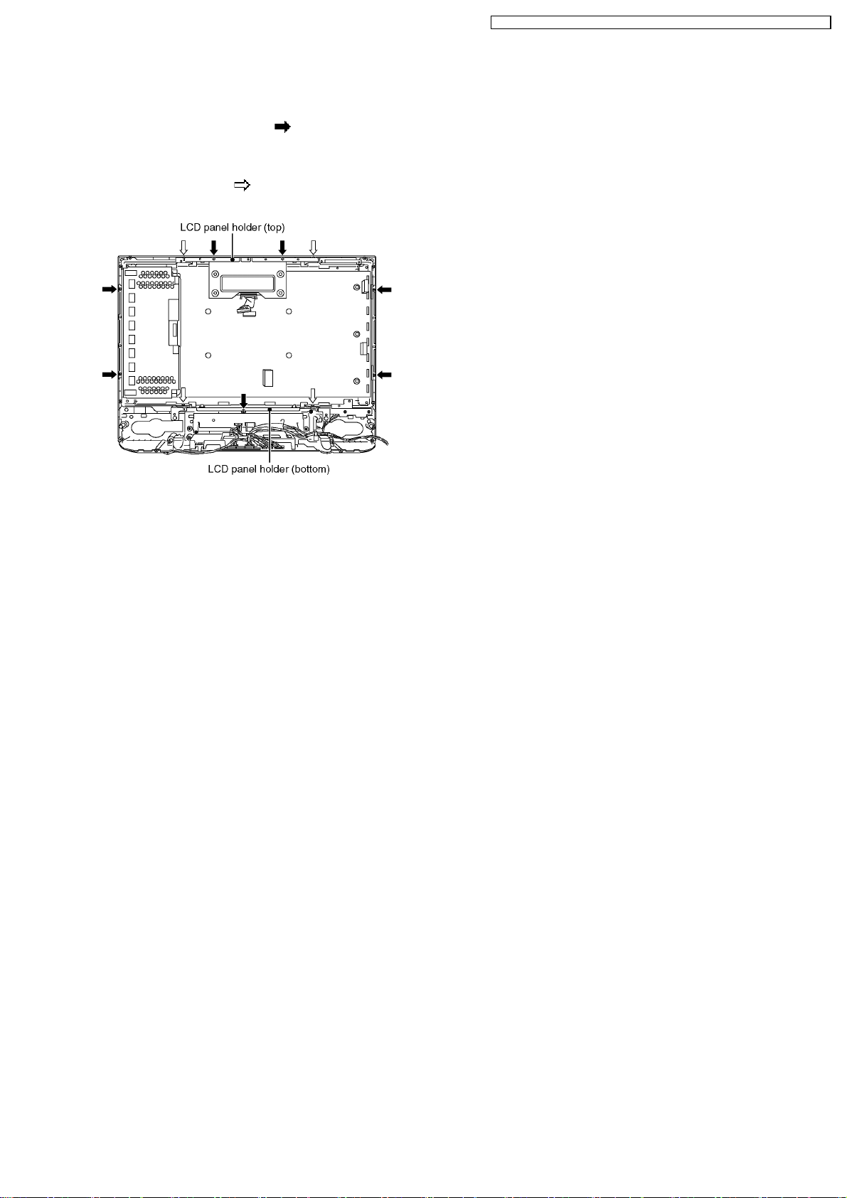
7.16. Removing the LCD panel
1. Remove the main chassis. (See 7.15.)
2. Remove the fixing screws (7pcs
3. Remove the LCD panel and LCD panel holders (right and
left).
4. Remove the screw (4pcs
5. Remove the LCD panel holders (top and bottom).
).
).
TX-32LXD50 / TX-26LXD50 / TX-32LX50F / TX-32LX50P / TX-26LX50F / TX-26LX50P
17

TX-32LXD50 / TX-26LXD50 / TX-32LX50F / TX-32LX50P / TX-26LX50F / TX-26LX50P
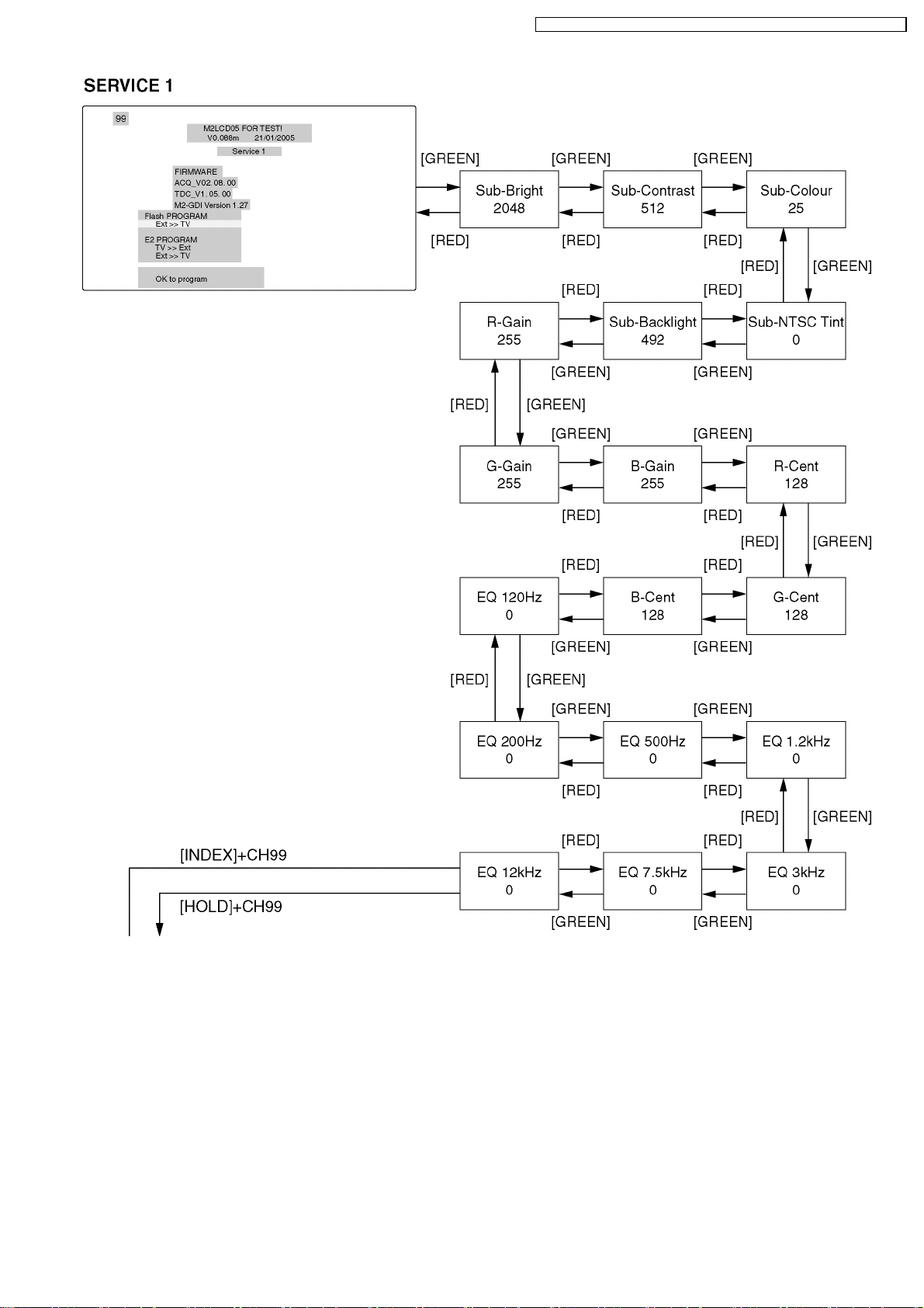
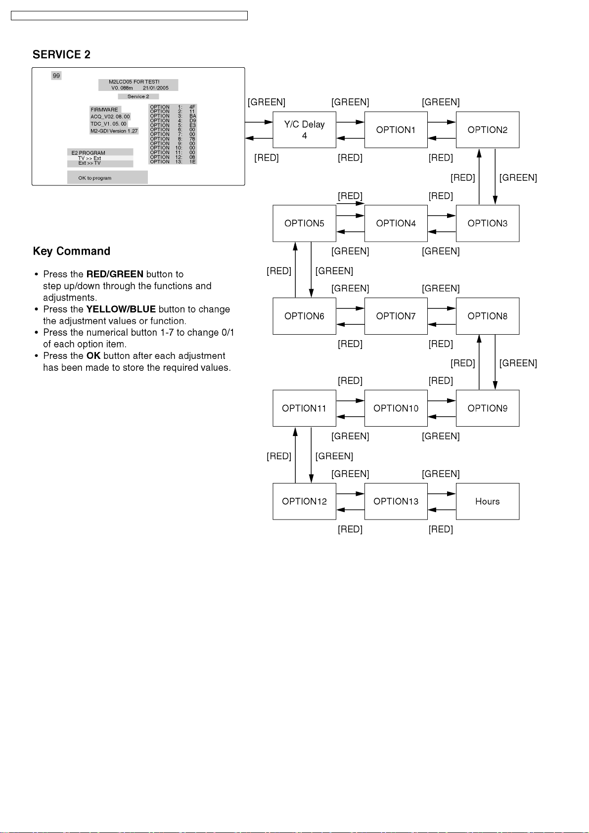
8 Service Mode Function
MPU controls the functions switching for each IICs through IIC bus in this chassis. The following setting and adjustment can be
adjusted by remote control in Service Mode.
8.1. How to enter SERVICE 1
1. In main menu, move to choose sound menu, set BASS to MAXIMUM, and set TREBLE to MINIMUM.
2. Simultaneously press INDEX button on remote control and DOWN button [
8.2. How to enter SERVICE 2
1. Enter the SERVICE 1 mode.
2. Set the channel to CH99.
3. Press HOLD button on remote control.
Note:
To exit to Service mode, press N or Power button on remote control.
] on the TV set.
18
TX-32LXD50 / TX-26LXD50 / TX-32LX50F / TX-32LX50P / TX-26LX50F / TX-26LX50P
19
TX-32LXD50 / TX-26LXD50 / TX-32LX50F / TX-32LX50P / TX-26LX50F / TX-26LX50P
20
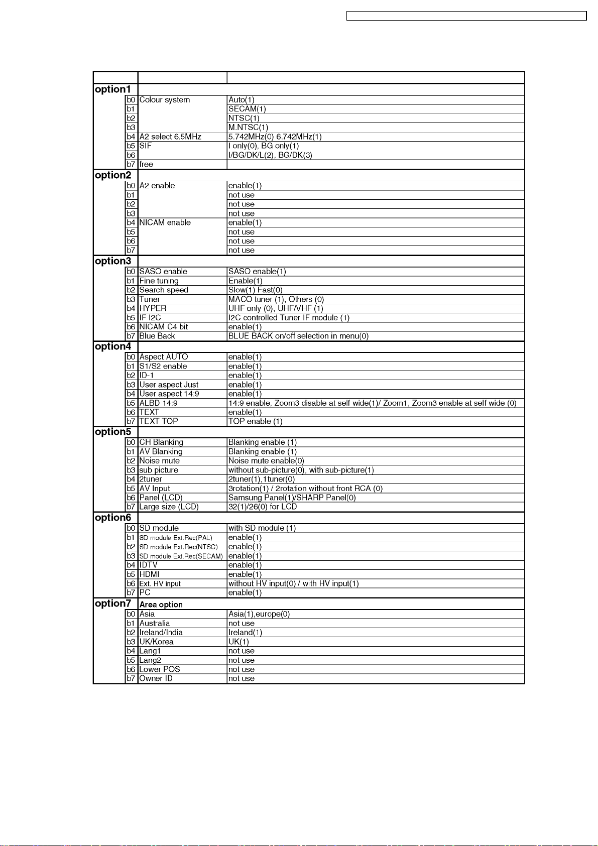
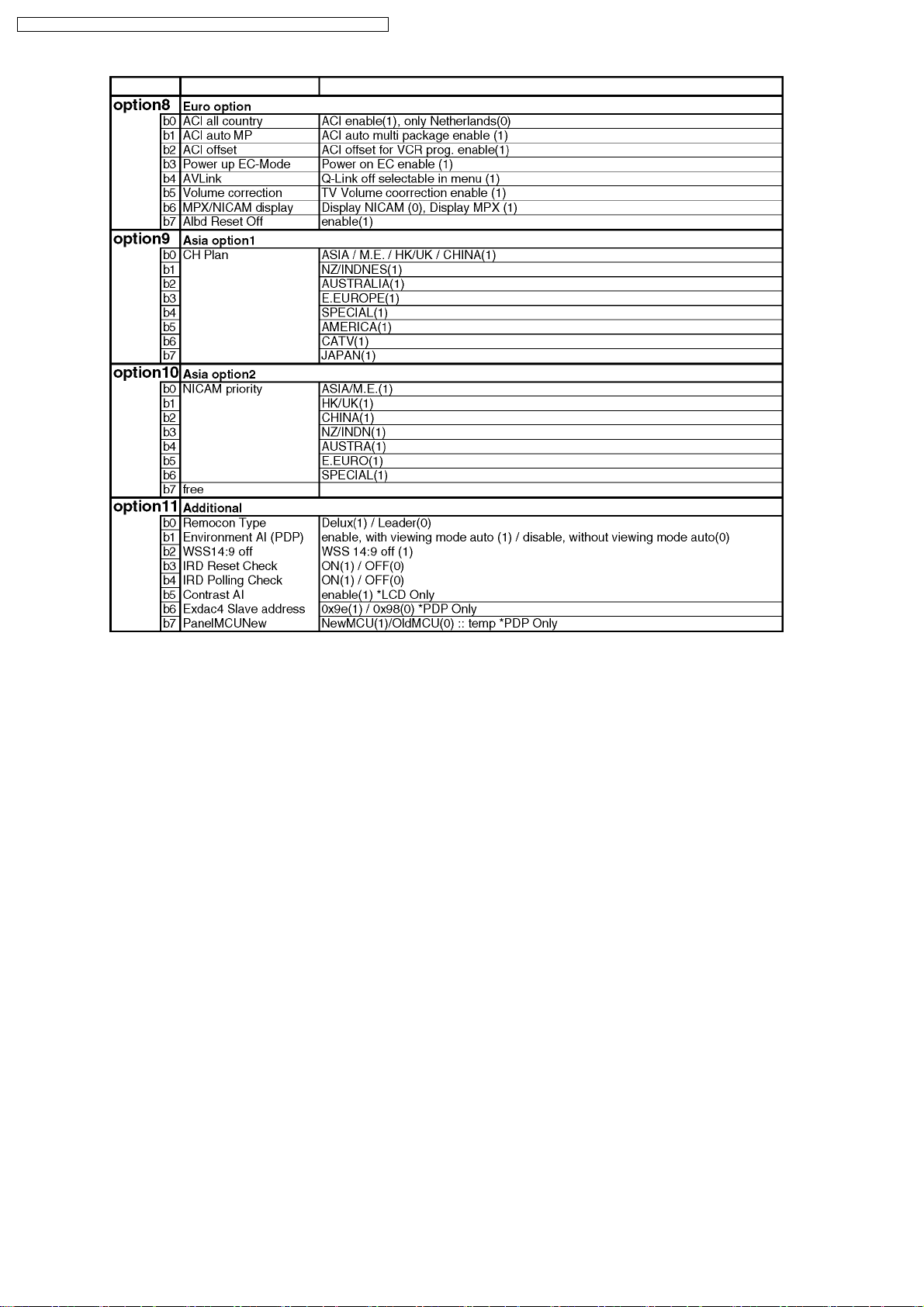
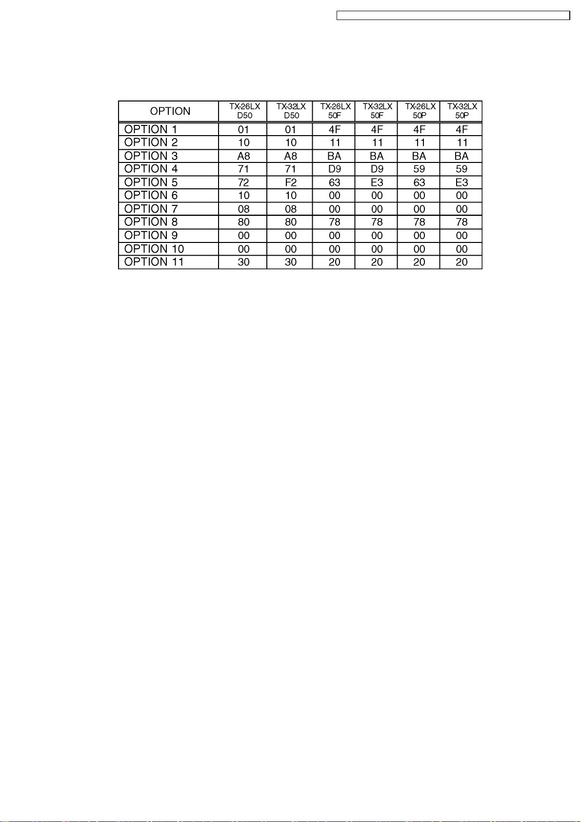
8.3. Option Description
TX-32LXD50 / TX-26LXD50 / TX-32LX50F / TX-32LX50P / TX-26LX50F / TX-26LX50P
21
TX-32LXD50 / TX-26LXD50 / TX-32LX50F / TX-32LX50P / TX-26LX50F / TX-26LX50P
22
TX-32LXD50 / TX-26LXD50 / TX-32LX50F / TX-32LX50P / TX-26LX50F / TX-26LX50P
8.4. Option Code Setting
If the memory IC (IC1107) or DG Board is replaced, option code should be re-memorized.
If you use for other model, you should re-memorized the different option code in SERVICE 2 mode.
23
TX-32LXD50 / TX-26LXD50 / TX-32LX50F / TX-32LX50P / TX-26LX50F / TX-26LX50P
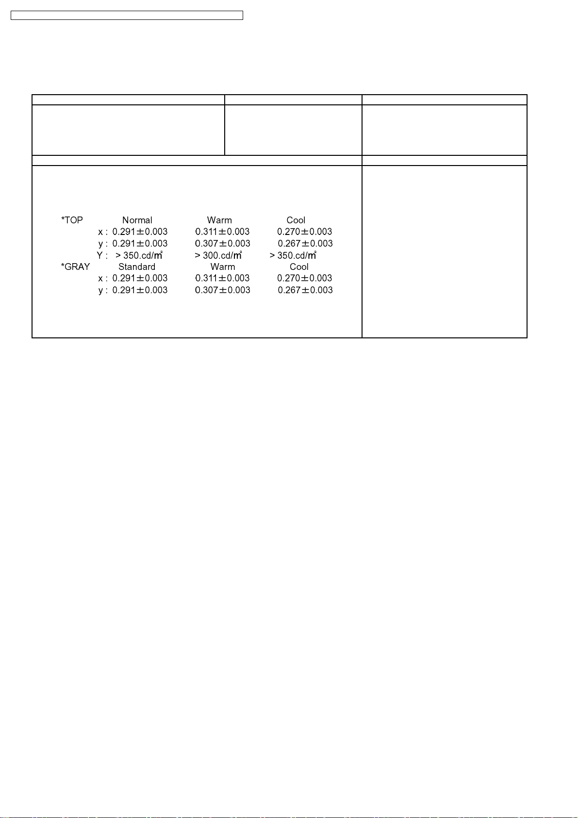
9 Adjustment method
9.1. White Balance Adjustment
Instrument Name Connect to Remarks
1. Remote controller
2. LCD WB meter (Minolta CS-1000A equivalent)
3. Communication jig
4. Computer for external control
Procedure Remarks
1. ProcedureBasically perform checking using the production software and make automatic
adjustment using external computer.
2. It adjusts in the mode of Colour balance Normal/ Warm / Cool as follows.
(UK/Euro model)
Correlation can be also taken by CA-210 or
equivalent
Let the panel stand for more than 3 hours at
more than 20 °C.
Basically perform assemble to completion in
the ambient environmen t of room temperature
more than 20 °C.
The aging time is more than 20 min at above
room temperature
* The address of EEPROM to write is as follows.
Add. C80-C91
24
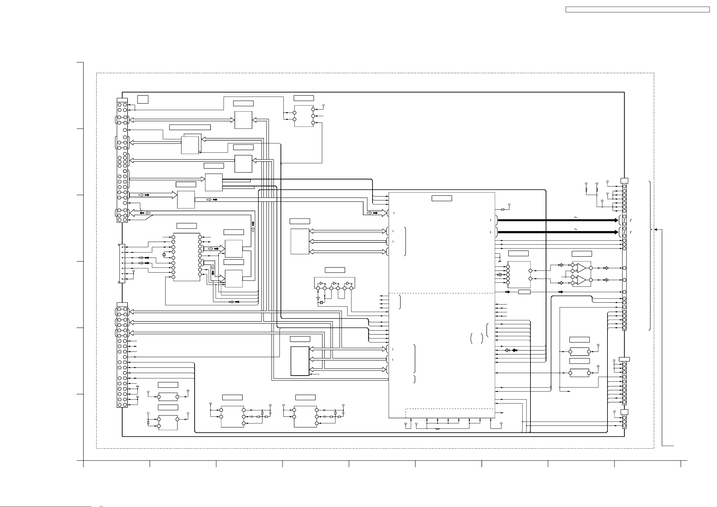
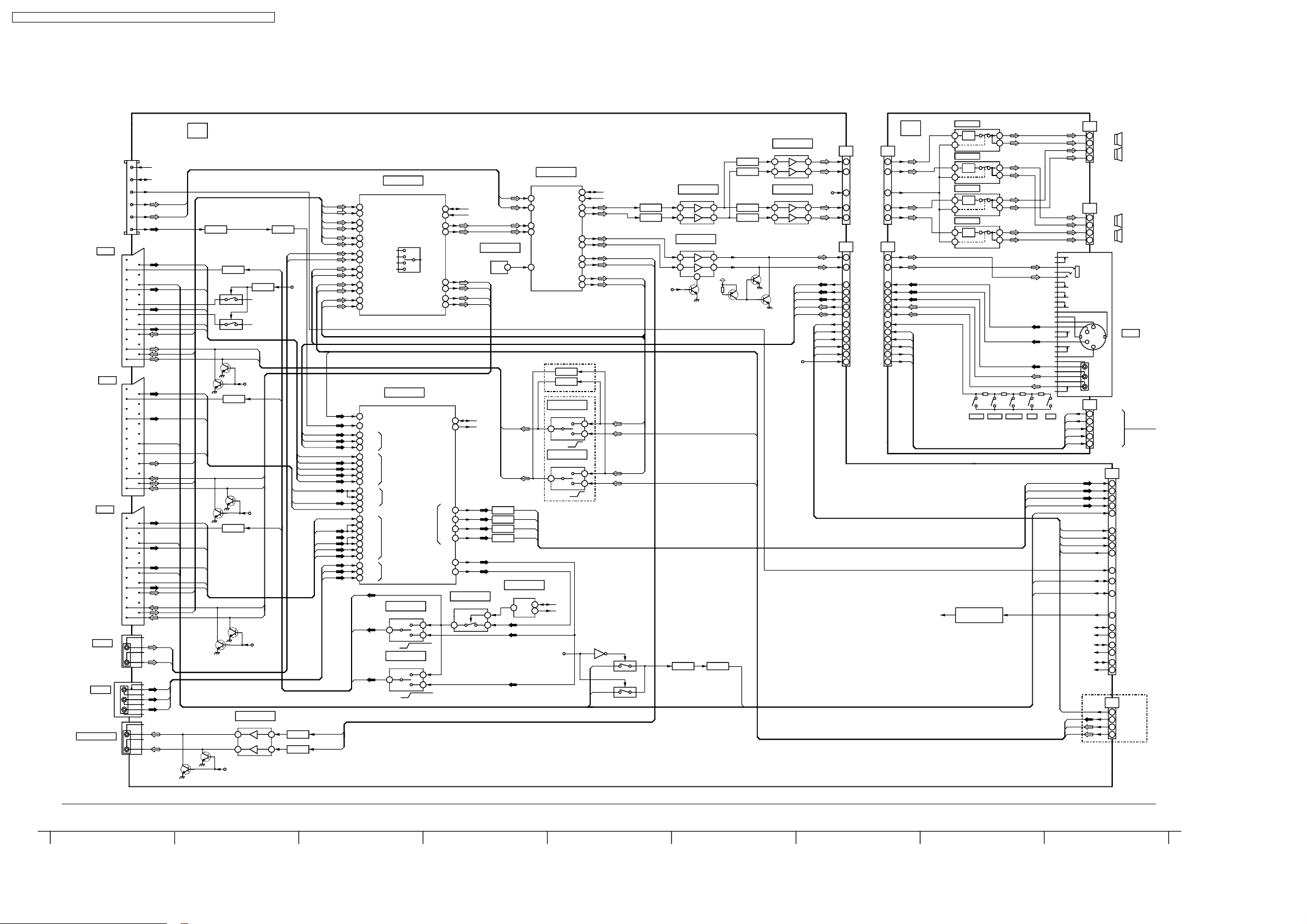
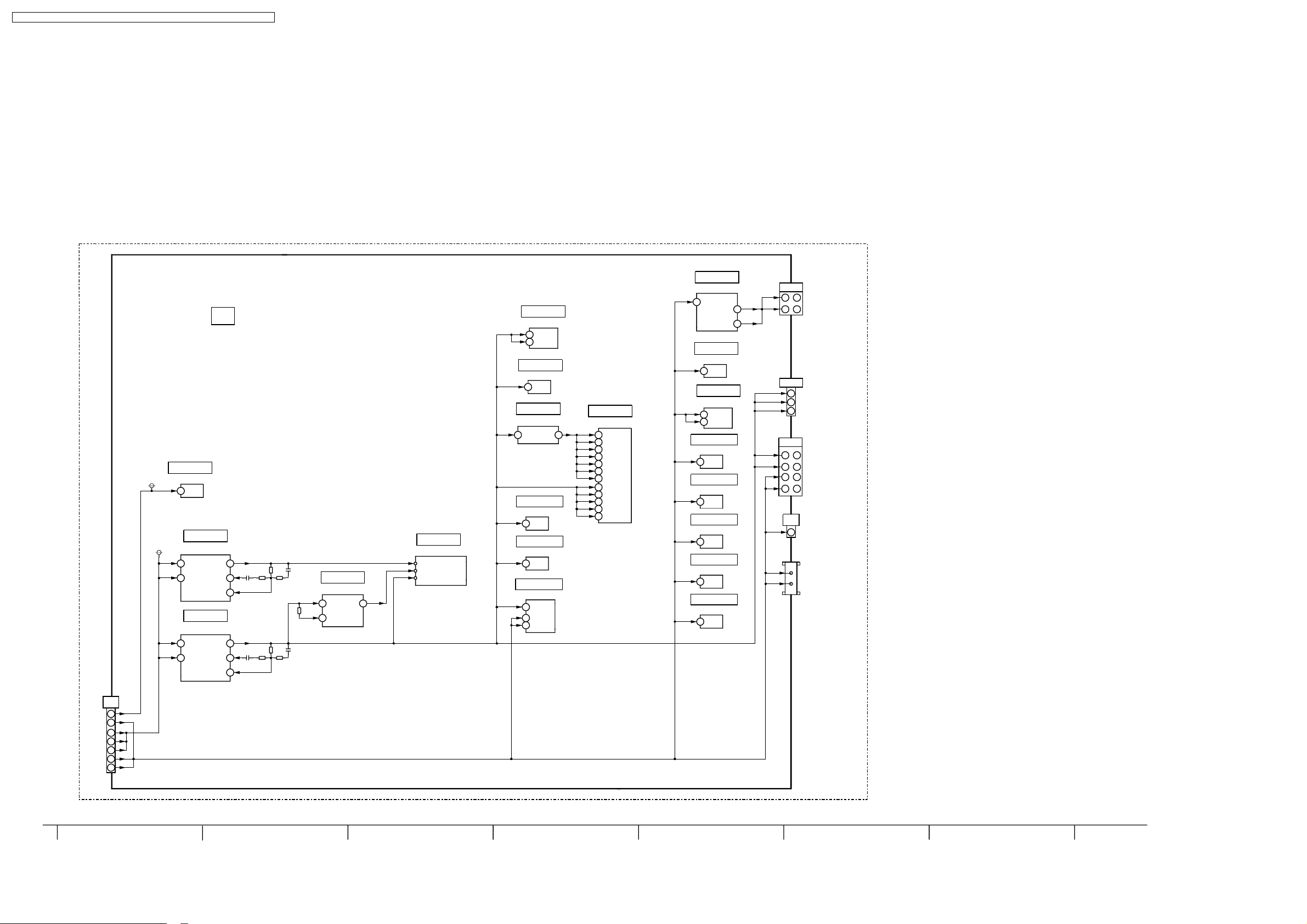
10 Block Diagram
10.1. Signal (1/3) Block Diagram
LXD50 ONLY
CI SLOT
(COMMON
A
B
C
D
E
F
INTERFACE)
Vpp1,Vpp2
D0~D7
RESET
A0~A14
CE1#,CE2#
OE#,WE#
IORD#,IOWR#
IREQ#
CD1#,CD2#
MCLK0,WAIT#
MOVAL,MOSTRT
MDO3~MDO7
MDO0~MDO2
MISTRT
MDI0~MDI7
MIBAL,MCLKI
TU8001
TV TUNER
ANT_V_SUPPLY
V_SUPPLY
SUPPORT
CARD
SLOT
ED16~ED31
EA0~EA24
CONTROL
BUS
SDA1,SDA0
SCL1.SCL0
TCK,TMS
TDI,TDO
SBO0,SBI0
XNMIRQ,XIRQ3
SUB 5V
SUB 5V
VCC
REG#
IF_AGC
XRST
XCD1
TRST
3.3V
3.3V
JK8401
18
17
2
30
10
21
7
9
44
36 67
37
64
47
53
19
SCL
4
SDA
5
IFD1
11
IFD2
10
9
1
7
JK8201
1
103
10
89
32 44
67 79
35
51
52
53
55
46
66
30
27
28
XV
52
51
6
32
58
8
14
29
61
42
15
45
16
5957
632062
41
66
46
50
56
8
110
23
101
36
60
59
88
58
57
54
65
45
8229
81
84
83
STROUT
SPEN,SPCLK
SUB 5V
XRST
SDA1,SDA0
SCL1,SCL0
XIRQ1
SUB 5V
3.3V
DATA
ADDRESS
CONTROL
CONTROL
3.3V
3.3V
X8003
24.167MHz
DATA
SPDATA0~7
XIRQ1
IC8864
AVR +1.8V
VIN
IC8034
AVR +2.5V
VCC1VOUT
CTL
IC8410,IC8411
BUFFER
IC8412
BUFFER
IC8003
COFDM DEMODULATOR
42
LOCK/OP2 SCL
VOUT
18
19
62
63
9
10
16
12
SCLT
SDAT
XTALI
XTALO
IMM
IMP
AGC1
RESET
17
42
ADDRESS BUS
CONTROL BUS
TCK,TMS
TDI,TDO
SBO0/SBI0
+1.8V
+2.5V
DATA B US
XCD1
TRST
STROUT
CLKOUT
D/#P
SDA
TX-32LXD50 / TX-26LXD50 / TX-32LX50F / TX-32LX50P / TX-26LX50F / TX-26LX50P
EA1-EA15
IC8402
DATA BUFFER
ED16-ED23
RESET
IC8401
CARD 5V
6
OUT
8
OUT
SUB 5V
7
IN
2
XIRQ2
FLG
1
EN
IC8404
CONTROL BUFFER
IC8213
BUFFER
CHCLK,CHVAL,CHSYNC
XCD1,XCD2,XWAIT,XIREQ
DATA
SCL1
SDA1
DC-DC CONV.3.3V
1
8
IC8408
TS BUFFER
IC8409
TS BUFFER
IC8023
VIN SW
PVIN
SPPKTST
SPCLK
SPEN
SPDATA7
XFERSTO
3.3V(1.1A)
2
FB
3
INV
4
20
21
34
D0
31
D3
23
29
D4
25
D7
36
38
SUB 9V
POWER
IC8009
256M DDR_SDRAM
IC8019
XCD1
64M CPU FLASH ROM
WP,WE,CE,OE
SUB 9V
DC-DC CONV.1.2V
1
8
DG0-DQ15
A0-A21
RESET
IC8024
VIN
PVIN
IC8501
VCXO27M
123456
X8006
XRST
2
SW
FB
3
INV
4
DATA B US
ADDRESS BUS
CONTROL BUS
1.2V(0.8A)
DATA B US
ADDRESS BUS
CONTROL BUS
POWER
RESET
XIREQ
XWAIT
XCD2
XCD1
CHCLK
CHVAL
CHSYNC
HSCLKIN
HSVALIN
HSSYNCIN
HSDIN0
HSDIN7
MMDQ0
MMDQ31
MMA0
MMA13
XECSO,XERE
XEWE2,PWP
XMNIRQ
XIRQ0
INTERRUPTION
XIRQ1
XIRQ2
CK27
VC27
CIPOWER
CIRESET
XIREQ
XWAIT
XCD2
XCD1
ED16
ED31
EA0
EA24
XECSO-XECS5
BOOTSWAP,XEDK
ELLK,XEWE2,XEWE3
XERE,ERXW
XIORD,XIOWR
XWE,XOE,REG
XECS3
DDRSDRAM
1.2V 3.3V
HDSL PEAKS_Lite
PEAKS_Lite(3/3)
PEAKS_Lite(1/3)
SUPPORT CARD&
NOR FLASH ROM
I/F
CI I/F
PEAKS_Lite(2/3)
IC8013
JTAG I/F
Joint
Tes t
Action
Group
IEC_OUT
MHSYNC0
MVSYNC0
MVCLK0
DACCK
XDACRST
EVTRG
DRSTMSK
XFERSTO
SCHDATA0
ENABLE0
CHPSYNC0
SCHCLK0
MVY0
MVY7
MVC0
MVC7
SRCK
DMIX
LRCK
CVBS
SCL0
SDA0
SCL1
SDA1
XRST
SBO1
SBI1
SBO0
SBI0
VDDQ
AVDDMVAVDDSVAVDDMAVDDDAVDDAAVDDVDD33VDD12
SUB 9V
FDC_A5VA5V
3.3V
MVY0
MVY7
MVC0
MVC7
DC
DY
IC8029
AUDIO DAC
MCLK
1
BICK
2
SDTI
3
4
LRCK
5
PDN
AOUTL
AOUTR
IC8031
OP AMP
11
10
SUB 9V
2
3
5
6
Q8101
SCL0
SDA0
SCL1
SDA1
EVTRG
TDO
TDI
TMS
TCK
TDO
TDI
TMS
TCK
TRST
XFERSTO
SPDATA7
SPEN
SPPKTST
SPCLK
IC8043
RESET
OUT
IC8042
RESET
VOUT
SBO1
2.5V
2.5V
(DDR SDRAM)
SBI1
SBI0
SBO0
XRST
SUB 5V
1
7
AF_VDACOUT5
SBO1
SBI1
XRST
3.3V
24
VDD
SUB 9V
21
VDD
SUB 9V
TCK
TMS
TDI
TDO
TRST
EVTRG
TRST
TMS
TDO
TDI
TCK
SUB 5V
XV01
TO DG1
SUB 9V
13
SUB 9V
51
SUB 9V
52
SUB 9V
53
54
SUB 5V
SUB 5V
57
SUB 5V
14
88
MVY0
96
MVY7
97
MVC0
105
MVC7
107
MHSYNC0
106
MVSYNC0
109
MVCLK0
DL
41
DL(BS_L)
DR
43
DR(BS_R)
CVBS
72
SBO1(SBI1)
18
SBI1(SBO1)
19
XRST
22
26
TCK
TMS
27
TDI
28
TDO
29
30
TRST
FOR
FACTORY
USE
(JTAG I/F)
3.3V
CN8202
2
3.3V
15
3.3V
16
3.3V
3
XRST
EVTRG
4
TRST
5
TMS
7
TDO
9
TDI
11
TCK
14
FOR
FACTORY
XV04
USE
1
+5V
2
SBI0
SBO0
3
(232C)
FOR
DEBUG
TX-32/26LXD50, TX-32/26LX50F/P Signal (1/3) Block Diagram TX-32/26LXD50, TX-32/26LX50F/P Signal (1/3) Block Diagram
2
54 91 68
73
25
TX-32LXD50 / TX-26LXD50 / TX-32LX50F / TX-32LX50P / TX-26LX50F / TX-26LX50P
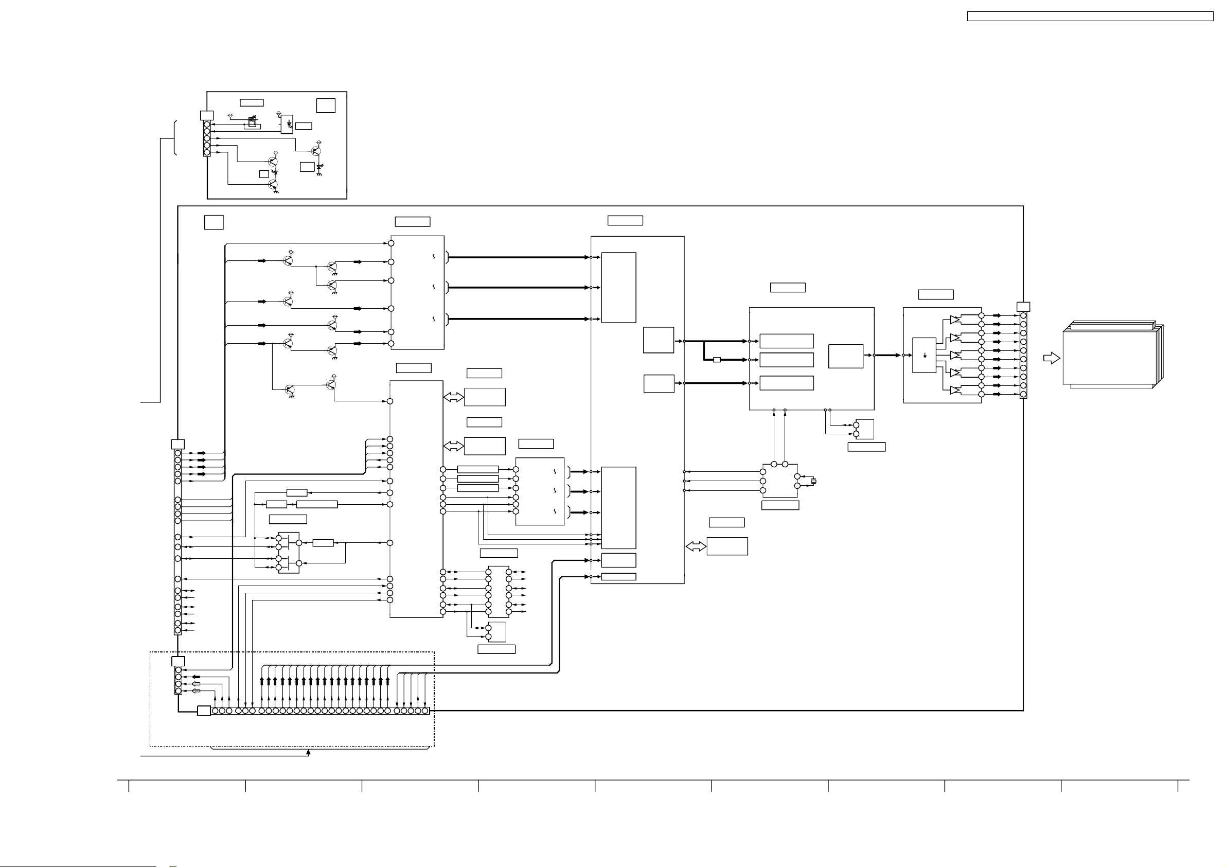
10.2. Signal (2/3) Block Diagram
H
TU3201
TUNER
JK3002
TV VIDEO OUT
JK3003
VIDEO OUT
Chroma in
JK3004
TV VIDEO OUT
JK2001
AV4C
AUDIO
JK3005
AV4C
JK2002
AUDIO OUT
AV1
VIDEO IN
FB IN
RED IN
GREEN IN
AV1 SL OW
BLUE IN
TV L OUT
TV R OUT
AV2
VIDEO IN
Q-LINK
AV2 SLOW
TV L OUT
TV R OUT
AV4
VIDEO IN
BLK IN
RED IN
GREEN IN
Q-LINK
AV1 SL OW
BLUE IN
TV L OUT
TV R OUT
SCL
SDA
AFT
AM
SIF
VIDEO
SDA2
SCL2
L IN
R IN
L IN
R IN
L IN
R IN
L
R
Y
PB
PR
SCL1
10
SDA1
11
12
13
14
17
21
20
19
18
17
16
15
14
13
12
11
10
9
8
7
6
5
4
3
2
1
21
20
19
18
17
16
15
14
13
12
11
10
9
8
7
6
5
4
3
2
1
21
20
19
18
17
16
15
14
13
12
11
10
9
8
7
6
5
4
3
2
1
AV2_Q-LINK
AV4_Q-LINK
AV1_FB
AV4_FB
AM
SIF
Q3202 Q3010
V
R
G
Q3006
SLOW
B
AV1_L
AV1_R
V
C
SLOW
AV2_L
AV2_R
V
R/C
G
SLOW
B
AV4_L
AV4_R
Q3002
Q3005
Q2009
Q3004
Q2006
Q3003
Q2010
Q2007
Q3002
SDA2
SCL2
AV1_LOUT
AV1_ROUT
MUTE
AV2_LOUT
AV2_ROUT
MUTE
AV4_LOUT
AV4_ROUT
Q2004
AV4C_L
WHITE
AV4C_R
RED
Y-SW
PB-G
PR-G
WHITE
Y
Y
Y-G
PB
PB
PR
PR
RED
Q2002
Q2001
MUTE
Q2003
IC2102
AMP
75
MUTE
AV1_VO
AV2_VO
AV4_VO
TO
IC2500
G
IC2303
AMP
AV4C_L
AV4C_R
FROM
IC3005
66pin
Q2114
5
31
5
31
FROM
T7101-13pin
STB LED
H.P.F.
7
1
9
MAIN5V
Q2017
H.P.F.
L.P.F.
L.P.F.
Q2115
IC2106
60
67
56
57
21
MONO IN
ANA IN
AV IN L
AV IN R
RESETQ
MSP
I2CDA
I2CCL
DACM L
DACM R
DACA L
DACA R
MON L
MON R
TV1 L
TV1 R
LX50F/P ONLY
SDA1
3
SCL1
2
28
27
25
24
37
36
34
33
TV1_LOUT
TV1_ROUT
Q2105
Q2104
MON_L
MON_R
IC2104
5
3
IC2101
HP AMP
2
47
MUTE
Q2113
AMP
10
IC2105
AUDIO SW
AV1_L
AV1_R
AV2_L
AV2_R
AV4_L
AV4_R
AV3_L
AV3_R
DVB_L
O2
DVB_R
TV1_L
TV1_R
DVB_V
1
L
R
2
3
L
R
4
9
L
R
10
18
L
R
19
7
L
R
8
14
L
R
15
16
L
R
17
22
SDA
23
SCL
L
29
30
R
L
25
26
R
L
34
35
R
SDA1
SCL1
AV2_LOUT
AV2_ROUT
AV4_LOUT
AV4_ROUT
IC2108
RESET
AM
SIF
4
Q2116
IC2302
AMP
7
7
AV3_Y
AV3_C
AV3_V
AV3_L
AV3_R
Q2117
IC3005
VIDEO SW
DVB_V
19
TV_V
AV3_V
AV3_Y
AV3_C
SLOW
V
R
G
B
V
C
SLOW
SLOW
V
R/C
G
B
31
Q2103
Q2104
17
77
V
AV3
79
Y
S-VIDEO
1
C
SLOW
68
V
65
AV1
R
29
SCART
G
27
B
31
71
V
AV2
72
Y
SCART
75
C
74
C
SLOW
4
V
3
Y
5
C
7
AV4
SCART
R
35
G
33
B
37
Y
39
MON_L
MON_R
AV1_VO
AV2_VO
AV4_VO
41
43
Y
Pb
Pr
Q-Link Sel TV MONITOR OUT
Q-Link Sel TV MONITOR OUT
AV4
COMPONENT
IC3001
Q-LINK SEL
2
IC3002
Q-LINK SEL
2
PB
PR
MAIN
6
4
6
4
VOUT
VOUT4
VOUT
SDA
SCL
PR
PB
V/Y
45
46
58
59
60
51
46
48
IC3004
AV1-SW
SDA1
AV1_ROUT
SCL1
AV1_LOUT
Q3011
Q3017
Q3014
Q3015
IC3006
EX.I/O
9
1
62
MAIN_PR
MAIN_PB
MAIN_Y/V
MAIN_CVBS
14
15
IC2112
DVB SEL
7
DVB Sel DVB TV
IC2111
DVB SEL
7
DVB Sel DVB TV
LXD50 ONLY
SDA1
SCL1
FROM
IC3005
72pin
O3
1
3
1
3
TV1_ROUT
DVB_R
TV1_LOUT
DVB_L
Q3020
AV4_FB
Q3019
AV1_FB
Q3016
Q3021 Q3022
FB
MUTE
H5
11
17
15
13
19
H4
29
30
11
14
7
22
26
21
16
20
8
17
4
SQ_L
SQ_R
MUTE
WF_L
WF_R
HP_LOUT
HP_ROUT
AV3Y (S)
AV3C (S)
AV3V
AV3_LIN
AV3_RIN
KEYSCAN
AI SENSOR
REMOTE
REC LED
STB LED
LED R
G5
11
17
15
13
19
G4
29
30
11
14
7
22
26
21
16
20
8
17
4
MUTE
AMP
7
IC2502
AMP
7
IC2501
AMP
7
IC2503
AMP
7
SW3806
Q2011,12,14
MUTE CIRCUIT
SQ L AMP
SQ R AMP
WF L AMP
WF R AMP
164
13
164
13
164
13
164
13
4
5
1
2
3
7
6
9
8
11
10
G
G
Y-G
Y
Y-SW
C
C-SW
C-G
V-G
V
L-G
L
R-G
R
R-SW
F STR-/DOWN+/UPTV/AV
SW3802SW3803SW3804SW3805
MAIN_PR
MAIN_PB
MAIN_Y/V
MAIN_CVBS
FB
AV2_QLINK
AV4_QLINK
DVB_V
DVB_L
DVB_R
G10
1
2
3
4
G11
1
2
4
5
G
HEADPHONE
R
L
G1
1
3
6
7
10
SDA1
SCL1
SDA2
SCL2
SDA3
SCL3
LXD50 ONLY
Y
C
V
L
R
SPEAKER
(L CH)
SQ_L +
SQ_L Woo_L +
Woo_L -
TO
SPEAKER
(R CH)
SQ_R +
SQ_R Woo_R +
Woo_R -
AI SENSOR
REMOTE
REC LED
LED R
STB LED
JK3801
H3
11
9
7
13
15
33
36
38
26
35
40
39
30
24
23
21
20
18
17
H2
24
6
8
10
SQ L
WF L
SQ R
WF R
AV3
MAIN_PR/B
MAIN_PB/C/R
MAIN_Y/V/G
MAIN_CVBS
FB_OUT
KEYSCAN
AI SENSOR
REMOTE
LED R
AFC1
AV2_QLINK
AV4_QLINK
SOUND_MUTE
SDA1
SCL1
SDA2
SCL2
SDA3
SCL3
REC LED
DVB_V
DVB_L
DVB_R
TX-32/26LXD50, TX-32/26LX50F/P Signal (2/3) Block Diagram TX-32/26LXD50, TX-32/26LX50F/P Signal (2/3) Block Diagram
181510 141311 1612 17
26
10.3. Signal (3/3) Block Diagram
Optica AI
AI SENSOR
REMOTE
REC LED
STB LED
LED R
SN1001
D1005
STB 3.3V
Red
STB 3.3V
VCC
GND
VOUT
Q1003
SUB_5V
V1
1
3
6
7
10
Q1004
RM1001
Remote
Amber
D1002
V
STB 3.3V
Q1001
TX-32LXD50 / TX-26LXD50 / TX-32LX50F / TX-32LX50P / TX-26LX50F / TX-26LX50P
MAIN_PR/B
MAIN_PB/C/R
MAIN_Y/V/G
MAIN_CVBS
KEYSCAN
AI SENSOR
AV2_QLINK
AV4_QLINK
SOUND_MUTE
REC LED
FB_OUT
REMOTE
LED R
AFC1
SDA1
SCL1
SDA2
SCL2
SDA3
SCL3
DVB_V
DVB_L
DVB_R
DG3
30
32
34
28
26
8
5
3
15
6
1
2
11
17
18
20
21
23
24
DG2
17
35
33
31
DG
MAIN_PR
MAIN_PB
MAIN_Y/V
MAIN_CVBS
SDA1
SCL1
SDA2
SCL2
SDA3
SCL3
LXD50 ONLY
IC4005
FB
MAIN_Y/V
MAIN_PB
MAIN_PR
MAIN_CVBS
Q4061
Q4054
Q4001
MAIN9V
MAIN9V
MAIN9V
Q4007
Q4008
Q4060
MAIN9V
Q4058
Q4004
MAIN9V
Q1105
51
76
77
74
72
57
121
FB
AIN6
SOY
AIN5
AIN4
AIN9
IC1104
CVBS
A/D
MICOM
RIN0
RIN3
UVIN0
UVIN9
YIN0
YIN9
IC1115
16M FLASH
IC1114
124
KEYSCAN
127
AI SENSOR
5
REMOTE
80
LED R
REC LED
16
FB
Q1109
Q1106,Q1107
Q1110
IC1105
Q-LINK SEL
3
5
4
1
2
Q1111
13
125
7
6
8
90
89
88
81
AFC1
Q-LINK OUT
Q-LINK IN
QLINK_SEL
SOUND_MUTE
IDTV_RXDO
IDTV_TXDO
IRD_RST
OSD R
OSD G
OSD B
VSYNC
HSYNC
SDA1
SCL1
SDA2
SCL2
SDA3
SCL3
BLK
64M SDRAM
IC4012
OSD RGB AD
112
Q4068,Q4032
113
Q4065,Q4031
114
Q4062,Q4030
102
103
105
98
97
75
74
101
100
IC1107
IC1109
3.3V<->5V
4
SDA1
5
SCL1
2
SDA2
3
SCL2
6
SDA3
7
SCL3
5
SDA
6
SCL
EEPROM
44
41
110
65
71
108
20
19
22
21
18
17
OSD R
OSD G
OSD B
VSYNC
HSYNC
OSD R0
OSD R3
OSD G0
OSD G3
OSD B0
BLK
OSD B3
SDA1
SCL1
SDA2
SCL2
SDA3
SCL3
IC4054
GC4PRO
PORT-A
PORT-D
(OSD INPUT)
PORT-C
(PEAKS)
JTAG
PORT-E
(RGBOUT)
PORT-F
(OSD-OUT)
95.5MHz to 4PRO(EXCLKIN)
108MHz to 4PRO(FRCLKIN)
81MHz to 4PRO(VCOIN)
IC4055
DDR SDRAM
IC4057
GC4L
PORT-A
(from GC4pro)
PORT-C
(from GC4PRO_E-Port)
PORT-D
(OSD)
74.25MHz to 4L(EXCLKIN)
108MHz to 4L(FRCLKIN)
10 7
1
8
9
IC4051
CLOCK GENE.
IC4033
LVD S T X
TA+
47
TA-
48
TCLK+
TCLK-
TB+
45
TB-
46
TC+
41
TC-
42
TD+
37
TD-
38
39
40
BUFFER
R/G/B
(8bit)
5
SDA
6
SCL
IC4052
EEPROM
HS/VS
CLK
PORT-E
(to LVDS)
4
X4002
5
TTL
PARALEL
DATA
LVDS
CONV.
DG7
18
RX0+
19
RX0-
15
RX1+
16
RX1-
12
RX2+
13
RX2-
6
RX3+
7
RX3-
9
RXCLK+
10
RXCLK-
LCD PANEL
107
10619109
105
100
102
103
MVC7
MVC7
MVC7
104
MVC7
MVC7
MHSYNC0
MVSYNC0
MVCLK0
2726 2928
30
TDI
TMS
TDO
TCK
TRST
88
SBI1(SBO1)
SBO1(SBI1)
89
22
MVY0
XRST
MVY190MVY291MVY392MVY493MVY7
72
43
41 18
DG3
CVBS
DL(BS_L)
DR(BS_R)
97
96
MVC0
MVY595MVY698MVC099MVC0
TX-32/26LXD50, TX-32/26LX50F/P Signal (3/3) Block Diagram TX-32/26LXD50, TX-32/26LX50F/P Signal (3/3) Block Diagram
20 2722 2421 23 262519
27
TX-32LXD50 / TX-26LXD50 / TX-32LX50F / TX-32LX50P / TX-26LX50F / TX-26LX50P
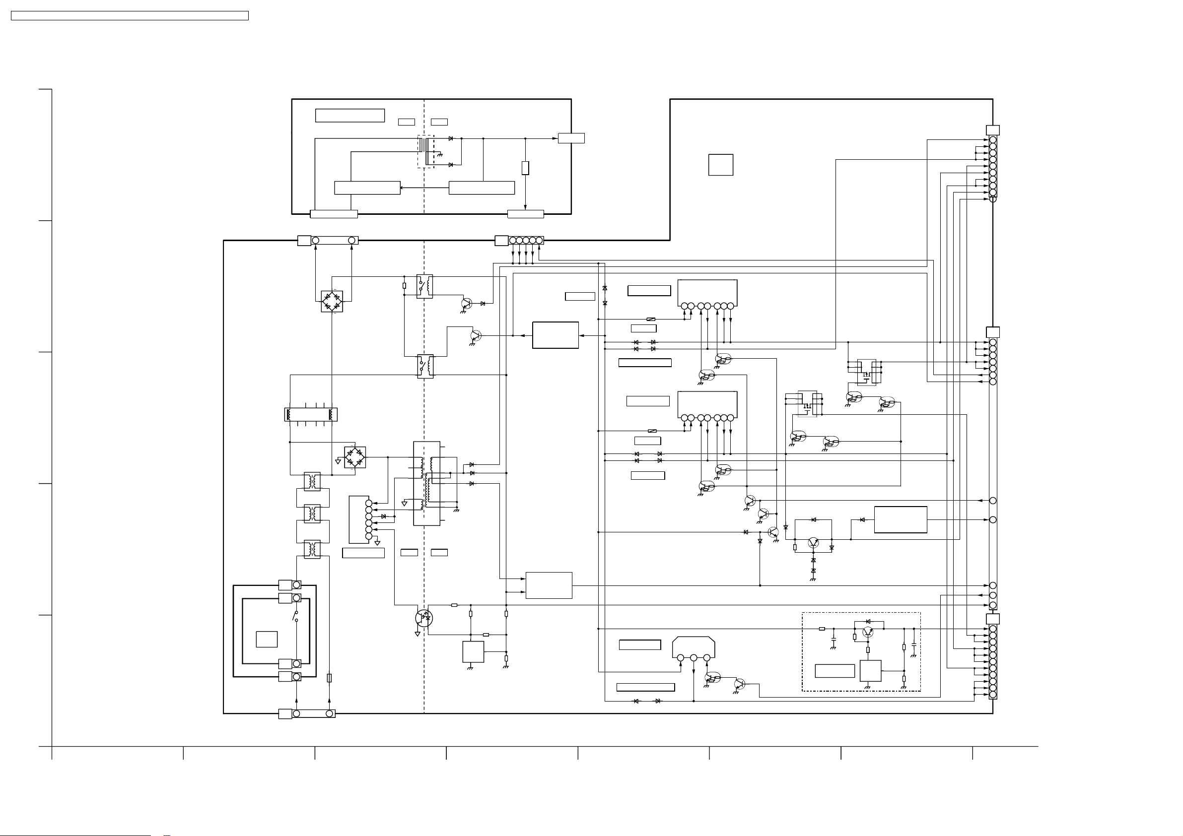
10.4. Power (1/3) Block Diagram
POWER UNIT
HOT
1converter
A
CONTROL POWER IC F.B. CIRCUIT
COLD
DC24V
LC Filter
INVERTER VCC
CN203
TO
LCD PANEL
AP
AP1
3
7
8
9
11
15
17
18
21
23
STB LED
SOUND 16V
SOUND 16V
SOUND 16V
MAIN 5V
SUB 5V
SUB 9V
SUB 9V
MAIN 3.3V
BT 30V
CN101 CN201
DC+
AP2
**
1
6NC7NC8
NC10NC11NC12NC
2
9
**
LF7002
2*3
*
1
LF7003
2*3
*
1
LF7004
2*3
*
1
1
1
D7004
**
L.F
4
L.FL.F
4
4
3m
B
C
NOISE FILTER
RECTIFICATION
L7001
D
AP8
K6
SW001
POWER SW
K
3
K6
3
E
AP8
*
*
- +
*
**
4
NC
3
**
RECTIFICATION
- +
*
*
*
*
*
*
IC7101
POWER CONTROL
F7000
DC-
17
RL7001
**
&
** **
D7202
Q7202
24V ERROR DET
RL7002
**
Q7203
AC ON/OFF
AC RELAY
D7107
VIN
7
VCC
4
S
5
D
8
FB
2
GND
3
T7101
STB TRANS.
2P2
*
3PT
4P1
*
6V2
7V1
HOT
COLD
PC7102
16NC
15S1
14S2C
*
13S2B
12S2A
11S3B
*
10S3C
9NC
FEED BACK
1
K
IC7103
ERROR DET
R
A
3
24V
24V
24V
24V
24V ON
7456
STB5V
1
OVP
CIRCUIT
Q7204-Q7207
ZERO CROSS
CIRCUIT
Q7101,Q7102
24V OVP
D7203
IC7301
DC/DC
D7204
SUUND_16V/SUB_5V
5V OVP
D7302
D7304
SOUND_16V OVP
IC7401
DC/DC
SUB_9V/MAIN_3.3V
9V OVP
D7404
D7402
3.3V OVP
IC7701
PANEL VCC
PANEL_Vcc OVP
D7704
ON/OFF2
V_IN
V_OUT2
V_IN
R7300
D7301
D7303
9
Q7301
V_IN
V_IN
R7400
9
D7403
D7401
Q7401
V_IN
V_OUT
2
D7703
410
410
ON/OFF
ON/OFF2
51
1
1
V_OUT2
Q7701
V_OUT114ON/OFF1
17 18
Q7302
V_OUT114ON/OFF1
17 18
Q7402
Q7212
V_OUT1
V_OUT1
Q7214
D7206
Q7702
AP5
SUB 5V
2
SUB 5V
3
SUB 5V
4
MAIN 5V
22
MAIN 5V
23
24V ON
10
AC ON
18
Q7503
Q7502
Q7505
Q7501
Q7504
D7211
Q7208
D7605
BT_30V
Q7601
D7603
D7604
LXD50 ONLY
*
IC7851
ERROR DET
1W
Q7506
+
MAIN ON
16
Q7210,Q7211
D7208
SHORT SOS CIRCUIT
BT 30V
SOS1(L:ABNORMAL)
D7606
D7851
3
CATHODE
2
ANODE
Q7851
A_9V
REFERENCE
+
1
AP4
17
19
11
7
17
3
4
8
9
10
13
14
20
21
22
SOS1
24V DET
PANEL5V ON
STB 5V
A 9V
MAIN 9V
MAIN 9V
MAIN 3.3V
MAIN 3.3V
MAIN 3.3V
SUB 9V
SUB 9V
PANEL 5V
PANEL 5V
PANEL 5V
AP3
2
TX-32/26LXD50, TX-32/26LX50F/P
Power (1/3) Block Diagram
AP2
2
1
FROM AC CORD
2 73
TX-32/26LXD50, TX-32/26LX50F/P
Power (1/3) Block Diagram
461 8
5
28
10.5. Power (2/3) Block Diagram
TX-32LXD50 / TX-26LXD50 / TX-32LX50F / TX-32LX50P / TX-26LX50F / TX-26LX50P
STB LED
SOUND 16V
SOUND 16V
SOUND 16V
MAIN 5V
SUB 5V
SUB 9V
SUB 9V
MAIN 3.3V
BT 30V
TU3201
TUNER
SUB 5V
SUB 5V
SUB 5V
MAIN 5V
MAIN 5V
24V ON
MAIN ON
24V DET
PANEL5V ON
STB 5V
MAIN 9V
MAIN 9V
MAIN 3.3V
MAIN 3.3V
MAIN 3.3V
SUB 9V
SUB 9V
PANEL 5V
PANEL 5V
PANEL 5V
AC ON
SOS1
A 9V
G
10 15 3514
SOS2
STB 3.3V
IC2106
262731 36 38
33
LED R
KEY SACN
8
MSP
AHVSUP
39
DVSUP
12
DVSUP
13
AVSUP
65
AVSUP
66
AI SENSOR
REMOTE
DG2
H5
SOUND 16V
1
SOUND 16V
2
SOUND 16V
3
SOUND 16V
4
SOUND 16V
5
H4
21 21
AI SENSOR
16
20
8
17
4
2
19
24
H2
REC LED
17
KEY SCAN
REMOTE
REC LED
LED R
STB LED
SUB 5V
STB 3.3V
G5
1
2
3
4
5
G4
16
20
8
17
4
2
19
H1
3
7
8
9
11
15
17
18
21
23
BTL
15
+B
2
BM
3
IC2101
HP AMP
VCC
6
P/SW
1
IC3001
SWITCH
3
VCC
IC3002
SWITCH
3
VCC
IC3004
SWITCH
3
VCC
IC3006
EX.I/O
VCC
16
SAO1
12
IC2302
AMP
8
VCC
IC2303
AMP
8
VCC
IC2111
TV/DVB SEL
6
VCC
IC2112
TV/DVB SEL
6
VCC
IC2102
AMP
8
VCC
IC2104
AMP
8
VCC
IC2105
AUDIO SW
VCC1
5
VCC2
6
IC3005
VIDEO SW
VCC1
8
VCC2
47
VCC3
57
IC2103
MSP 8V
IN
3
IC2107
MSP 5V
VIN
1
ON/OFF
2
D3023
OUT
1
VO
3
VO
6
D3021
Q3008,Q3009
SOS DET CIRCUIT
MSP 8V/MSP 5V
SUB9V
SOS2(L:ABNORMAL)
IC2108
RESET
VDD
2
H
H3
DG3
IC2500
SQ AMP(L)
VDDA
5
VDDP
18
IC2501
WF AMP(L)
VDDA
5
VDDP
18
KEY MATRIX
IC2502
SQ AMP(R)
VDDA
5
VDDP
18
IC2503
WF AMP(R)
VDDA
5
VDDP
18
Optica AI
SUB 5V
REMOTE
STB 3.3V
REC LED
STB LED
LED R
V1
1
2
3
5
6
7
10
SN1001
G1
1
AI SENSOR
2
3
5
6
7
10
Q1004
VCC
GND
VOUT
Q1003
D1005
Red
V
RM1001
Remote
Q1001
D1002
Amber
DG5
2
DG4
3
4
22
23
10
18
16
17
19
11
7
17
3
4
8
9
10
13
14
20
21
22
IC1106
EX.I/O
VCC
16
SAO2
13
IC1108
RESET
IC1107
EEPROM
IC1109
5V<->3.3V
24
IC1105
Q-LINK SEL
14
IC1110
STB 3.3V
4
3
IC1103
STB 2.5V
2
1
VDD
VCC
VCC
VCC
VIN
ON/OFF
VIN
VC
SW3
10
IC1115
FLASH MEMORY
VCC
37
BYTE
47
IC1114
2
8
VO
5
VO
3
SDRAM
VDD
1
VDDQ
3
VDDQ
9
VDD
14
VDDQ
43
VDDQ
49
IC1104
VDD33-1
14
VDD33-2
32
VDD33-3
42
VDD33-4
53
VDD33-5
61
VDD33-6
69
VDD33-7
85
106
VDD33-8
VDD25-1
21
VDD25-2
87
111
VDDA-1
116
VDDA-2
119
VDDA-3
123
VDDA-4
MICOM
AI SENSOR
REC LED
24V DET
PANEL5V ON
MAIN ON
MAIN SENSE
SUB SENSE
LED R
REMOTE
24V ON
AC ON
INV ON
D1104
SOS1
SOS
97
80
124KEY SACN
5
127
16
78
92
12
79
94
97
10
11
SOS2
IC1117
INVERTER
VCC
5
IC4033
LVDS TX
VCC
9
VCC
26
PLL VCC
34
LVDS VCC
66
IC4051
CLOCK GENE.
VDD
2
AVDD
14
IC4052
EEPROM
VCC
8
IC4025
MAIN 1.8V
VIN
1
VIN
8
5
EN
IC4024
MAIN1.2V
VIN
1
EN
7
IC4008
OSD AD 3.3V
MAIN5V
VCONT
1
VOUT
5
VIN
IC4049
AD 3.3V
OUT
IN
3
VOUT
IC4041
1.8V
VOUT
VDD
SW
2
VO
2
1
IC4012
OSD AD
VDD
2
VDD
11
VDD
21
VDD
53
VDD
68
VDD
72
VDD
82
XSM
89
XTST
90
VDD
92
VDD
35
VDD
49
105
VDD
116
3
VDD
IC4048
DDR 2.6V
VIN
2
1
VC
IC4014
BUFFER
VDD
5
IC4005
AD
AVDD
2
4
5
63
PVDD
47
PVDD
48
DVDDIO
6
DVDDIO
18
DVDD
12
DVDD
39
DVDD
90
IC4042
MAIN 2.5V
VCC
2
1
CTL
IC4055
DDR
DDR 2.6V
VO
3
IC4044
1.2V
VDD
1
IC4061
OUT
4
1.2V
VDD
1
VOUT
VOUT
5
5
IC4080
DDR CLK
VDDQ
4
VDDQ
8
VDDQ
11
VDDQ
18
VDDQ
21
VDDQ
25
IC4054
GC4PRO
DDR 2.6V
MAIN 3.3V
MAIN 1.2V
1.2V
1.2V
IC4057
GC4L
MAIN 2.5V
MAIN 3.3V
MAIN 1.8V
IC4063
RESET
VDD
2
CURRENT
INV PWM1
Q4049
Q4050
Q4053
Q4052
DG
LXD50 ONLY
DG6
DG7
DG1
31
30
29
28
27
13
14
51
52
53
54
57
2
3
4
5
6
TO
LCD PANEL
(INVERTER)
INV SOS
INV ON
CURRENUT
INV PWM1
INV PWM2
TO
LCD PANEL
PANEL 5V
PANEL 5V
PANEL 5V
PANEL 5V
PANEL 5V
A 9V
SUB 5V
SUB 9V
SUB 9V
SUB 9V
SUB 5V
SUB 5V
TX-32/26LXD50, TX-32/26LX50F/P
Power (2/3) Block Diagram
8
TX-32/26LXD50, TX-32/26LX50F/P
Power (2/3) Block Diagram
119 1410
151312
29
TX-32LXD50 / TX-26LXD50 / TX-32LX50F / TX-32LX50P / TX-26LX50F / TX-26LX50P
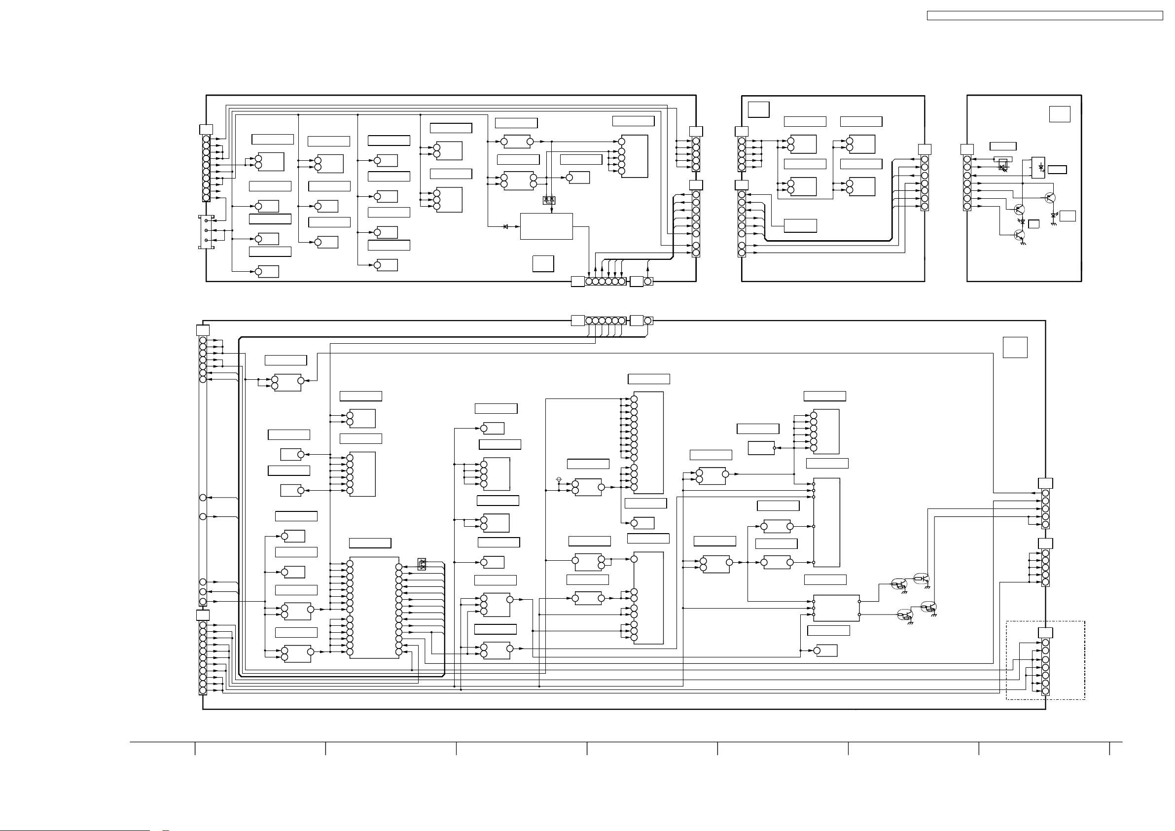
10.6. Power (3/3) Block Diagram
LXD50 ONLY
XV
IC8031
OP AMP
A9V
8
VDD
SUB 9V
IC8024
DC-DC CONV.1.2V
1
VIN
8
PVIN
INV
IC8023
DC-DC CONV.3.3V
1
8
PVIN
INV
2
SW
FB
3
4
2
SWVIN
FB
3
4
IC8034
AVR +2.5V
24
VOUT
VCC
1
CTL
IC8013
HDSL PEAKS_Lite
1.2V
+2.5V
3.3V
IC8019
64M CPU FLASH ROM
VCC
37
VIO
47
IC8043
RESET
2
VDD
IC8864
AVR +1.8V
VOUT
1
7
VIN
IC8412
BUFFER
VCC
20
IC8412
BUFFER
VCC
20
IC8402
DATA BUFFER
VCCA
1
VCCB
23
VCCB
24
IC8003
COFDM DEMODULATOR
VCCA1.8
2
DVCCA1.8
3
VDD
13
VDD
28
VDD
39
VDD
57
VCCXTAL1.8
61
PGAVCC3.3
8
VDD3.3V
22
VDD3.3V
35
VDD3.3V
44
VDD3.3V
52
IC8401
CARD 5V
7
IN
IC8042
RESET
2
VDD
IC8029
AUDIO DAC
VDD
14
P/S
9
IC8404
BUFFER
VCC
20
IC8408
BUFFER
VCC
20
IC8409
BUFFER
VCC
20
IC8410
BUFFER
VCC
20
IC8411
BUFFER
VCC
20
CI SLOT
(COMMON
INTERFACE)
JK8401
18
Vpp1,Vpp2
52
17
6
OUT
8
OUT
51
CN8202
JK8201
84
83
82 29
81
XV04
2
3.3V
15
3.3V
16
3.3V
27
28
30
1
+5V
ANT_V_SUPPLY
1
V_SUPPLY
7
VCC
FOR
FACTORY
USE
(JTAG I/F)
SUPPORT
CARD
SLOT
3.3V
3.3V
SUB 5V
SUB 5V
FOR
FACTORY
USE
TU8001
DVB TUNER
XV01
13
A 9V
14
SUB 5V
51
SUB 9V
52
SUB 9V
53
SUB 9V
54
SUB 5V
57
SUB 5V
TX-32/26LXD50, TX-32/26LX50F/P Power (3/3) Block Diagram
TX-32/26LXD50, TX-32/26LX50F/P
Power (3/3) Block Diagram
18 2221201916 17 23
30
 Loading...