

Page 1

ORDER NO.ITD1308049CE
FULL HD LCD Display
Model No. TH-50LFE6W
LA45 Chassis
© Panasonic Corporation 2013
Unauthorized copying and distribution is a violation
of law.
Page 2

TH-50LFE6W
TABLE OF CONTENTS
1 Safety Precautions -----------------------------------------------3
1.1. General Guidelines ----------------------------------------3
1.2. Touch-Current Check--------------------------------------3
2Warning--------------------------------------------------------------4
2.1. Prevention of Electrostatic Discharge (ESD)
to Electrostatically Sensitive (ES) Devices ----------4
2.2. About lead free solder (PbF) ----------------------------5
3 Service Navigation------------------------------------------------6
3.1. Service Hint--------------------------------------------------6
3.2. Applicable signals ------------------------------------------7
4 Specifications ------------------------------------------------------8
5 Service Mode -------------------------------------------------------9
5.1. CAT (Computer Aided Test) mode ---------------------9
5.2. IIC mode structure (following items value is
sample data)----------------------------------------------- 13
6 Troubleshooting Guide---------------------------------------- 14
6.1. Self Check ------------------------------------------------- 14
6.2. No Power--------------------------------------------------- 18
6.3. No Picture -------------------------------------------------- 18
7 Disassembly and Assembly Instructions --------------- 19
7.1. PCB Layout ------------------------------------------------19
7.2. Preparation ------------------------------------------------ 19
7.3. About disassembly and replacement --------------- 19
7.4. Back Cover removal ------------------------------------- 20
7.5. A-Board replacement------------------------------------ 20
7.6. P-Board replacement------------------------------------ 21
7.7. FR-Board replacement---------------------------------- 22
7.8. GK-Board and Key Button Bracket
replacement ----------------------------------------------- 22
7.9. Speaker Unit L/R replacement------------------------ 23
7.10. K-Board, LED Panel and LED Panel Case
replacement ----------------------------------------------- 23
7.11. Rear Panel BTM Assy replacement ----------------- 23
7.12. Rear Panel Top/L/R Assy replacement------------- 23
7.13. Rear Panel Metal Bot L/R replacement------------- 24
7.14. Metal Bracket Bottom replacement ------------------ 24
7.15. Rear Panel Metal Top/L/R replacement ------------ 25
7.16. LCD Panel replacement -------------------------------- 26
7.17. Caution about the sticking parts of LCD Panel --- 28
8 Block Diagram --------------------------------------------------- 31
8.1. Diagram Notes -------------------------------------------- 31
8.2. Main Block Diagram ------------------------------------- 32
8.3. Block (1 of 3) Diagram ---------------------------------- 33
8.4. Block (2 of 3) Diagram ---------------------------------- 34
8.5. Block (3 of 3) Diagram ---------------------------------- 35
9 Wiring Connection Diagram --------------------------------- 37
9.1. Wiring Connection Diagram --------------------------- 37
PAG E PAG E
2
Page 3

TH-50LFE6W
1 Safety Precautions
1.1. General Guidelines
1. When conducting repairs and servicing, do not attempt to modify the equipment, its parts or its materials.
2. When wiring units (with cables, flexible cables or lead wires) are supplied as repair parts and only one wire or some of the
wires have been broken or disconnected, do not attempt to repair or re-wire the units. Replace the entire wiring unit instead.
3. When conducting repairs and servicing, do not twist the Fasten connectors but plug them straight in or unplug them straight
out.
4. When servicing, observe the original lead dress. If a short circuit is found, replace all parts which have been overheated or
damaged by the short circuit.
5. After servicing, see to it that all the protective devices such as insulation barriers, insulation papers shields are properly
installed.
6. After servicing, make the following leakage current checks to prevent the customer from being exposed to shock hazards.
1.2. Touch-Current Check
1. Plug the AC cord directly into the AC outlet. Do not use an isolation transformer for this check.
2. Connect a measuring network for touch currents between each exposed metallic part on the set and a good earth ground
such as a water pipe, as shown in Figure 1.
3. Use Leakage Current Tester (Simpson 228 or equivalent) to measure the potential across the measuring network.
4. Check each exposed metallic part, and measure the voltage at each point.
5. Reserve the AC plug in the AC outlet and repeat each of the above measure.
6. The potential at any point (TOUCH CURRENT) expressed as voltage U
For a. c.: U1 = 35 V (peak) and U2 = 0.35 V (peak);
For d. c.: U
Note:
The limit value of U
mA d. c.
The limit value U
7. In case a measurement is out of the limits specified, there is a possibility of a shock hazard, and the equipment should be
repaired and rechecked before it is returned to the customer.
= 1.0 V,
1
= 0.35 V (peak) for a. c. and U1 = 1.0 V for d. c. correspond to the values 0.7 mA (peak) a. c. and 2.0
2
= 35 V (peak) for a. c. correspond to the value 70 mA (peak) a. c. for frequencies greater than 100 kHz.
1
and U2, does not exceed the following values:
1
Figure 1
3
Page 4

TH-50LFE6W
2Warning
2.1. Prevention of Electrostatic Discharge (ESD) to Electrostatically Sensitive (ES) Devices
Some semiconductor (solid state) devices can be damaged easily by static electricity. Such components commonly are called Electrostatically Sensitive (ES) Devices. Examples of typical ES devices are integrated circuits and some field-effect transistors and
semiconductor “chip” components. The following techniques should be used to help reduce the incidence of component damage
caused by electrostatic discharge (ESD).
1. Immediately before handling any semiconductor component or semiconductor-equipped assembly, drain off any ESD on your
body by touching a known earth ground. Alternatively, obtain and wear a commercially available discharging ESD wrist strap,
which should be removed for potential shock reasons prior to applying power to the unit under test.
2. After removing an electrical assembly equipped with ES devices, place the assembly on a conductive surface such as aluminum foil, to prevent electrostatic charge buildup or exposure of the assembly.
3. Use only a grounded-tip soldering iron to solder or unsolder ES devices.
4. Use only an anti-static solder removal device. Some solder removal devices not classified as “anti-static (ESD protected)” can
generate electrical charge sufficient to damage ES devices.
5. Do not use freon-propelled chemicals. These can generate electrical charges sufficient to damage ES devices.
6. Do not remove a replacement ES device from its protective package until immediately before you are ready to install it. (Most
replacement ES devices are packaged with leads electrically shorted together by conductive foam, aluminum foil or comparable conductive material).
7. Immediately before removing the protective material from the leads of a replacement ES device, touch the protective material
to the chassis or circuit assembly into which the device will be installed.
Caution
Be sure no power is applied to the chassis or circuit, and observe all other safety precautions.
8. Minimize bodily motions when handling unpackaged replacement ES devices. (Otherwise ham less motion such as the brushing together of your clothes fabric or the lifting of your foot from a carpeted floor can generate static electricity (ESD) sufficient
to damage an ES device).
4
Page 5

TH-50LFE6W
2.2. About lead free solder (PbF)
Note: Lead is listed as (Pb) in the periodic table of elements.
In the information below, Pb will refer to Lead solder, and PbF will refer to Lead Free Solder.
The Lead Free Solder used in our manufacturing process and discussed below is (Sn+Ag+Cu).
That is Tin (Sn), Silver (Ag) and Copper (Cu) although other types are available.
This model uses Pb Free solder in it’s manufacture due to environmental conservation issues. For service and repair work, we’d
suggest the use of Pb free solder as well, although Pb solder may be used.
PCBs manufactured using lead free solder will have the PbF within a leaf Symbol PbF stamped on the back of PCB.
Caution
• Pb free solder has a higher melting point than standard solder. Typically the melting point is 50 ~ 70 °F (30~40 °C) higher. Please
use a high temperature soldering iron and set it to 700 ± 20 °F (370 ± 10 °C).
• Pb free solder will tend to splash when heated too high (about 1100 °F or 600 °C).
If you must use Pb solder, please completely remove all of the Pb free solder on the pins or solder area before applying Pb solder. If this is not practical, be sure to heat the Pb free solder until it melts, before applying Pb solder.
• After applying PbF solder to double layered boards, please check the component side for excess solder which may flow onto the
opposite side. (see figure below)
Suggested Pb free solder
There are several kinds of Pb free solder available for purchase. This product uses Sn+Ag+Cu (tin, silver, copper) solder. However, Sn+Cu (tin, copper), Sn+Zn+Bi (tin, zinc, bismuth) solder can also be used.
5
Page 6

TH-50LFE6W
3 Service Navigation
3.1. Service Hint
Board Name Function
P-Board Power supply
Non serviceable.
P-Board should be exchanged for service.
A-Board Digital core signal processor
Non serviceable.
A-Board should be exchanged for service.
FR-Board Double speed processor
GK-Board Switch
K-Board Power LED, Remote receiver, C.A.T.S. sensor
Non serviceable.
FR-Board should be exchanged for service.
Non serviceable.
GK-Board should be exchanged for service.
Non serviceable.
K-Board should be exchanged for service.
6
Page 7

3.2. Applicable signals
TH-50LFE6W
7
Page 8

TH-50LFE6W
4 Specifications
Power Source 220-240 V AC, 50/60Hz
Power Consumption
Rated Power Consumption 90 W
Stand-by condition 0.5 W
Power off condition 0.5 W
Sound
Speakers 22 mm × 90 mm × 2 pcs
Audio Output 10 W [5 W + 5 W] (10 % THD)
LCD Display panel 50-inch VA panel (LED backlight), 16:9 aspect ratio
Screen size 1,095 mm (W) × 616 mm (H) × 1,257 mm (diagonal)
(No. of pixels) 2,073,600 (1,920 (W) × 1,080 (H))
[5,760 × 1,080 dots]
Operating condition
Temperature 0 °C - 40 °C
Humidity 20 % - 80 %
Applicable signals
Scanning format
PC signals VGA, SVGA, XGA, SXGA
Connection terminals
HDMI TYPE A Connector
DVI-D IN DVI-D 24 Pin Compliance with DVI Revision 1.0
AUDIO Stereo mini jack (M3) × 1 0.5 Vrms, Shared with PC IN
PC IN High-Density Mini D-sub 15 Pin G with sync 1.0 Vp-p (75 Ω)
AUDIO Stereo mini jack (M3) × 1 0.5 Vrms, Shared with DVI-D IN
LAN
SERIAL IN External Control Terminal
AUDIO OUT Stereo mini jack (M3) × 1 0.5 Vrms
Accessories Supply
Remote Control Transmitter N2QAYB000691
Batteries R6 Size × 2
Cable tie TMM17499 × 2
Ferrite core J0KG00000014 × 2
Dimensions (W × H × D) 1,121 mm × 655 mm × 49 mm
Mass (weight) approx. 18.0 kg
Note:
• Design and specifications are subject to change without notice. Mass and dimensions shown are approximate.
525 (480) / 60i 60p, 625 (575) / 50i 50p, 750 (720) / 60p 50p, 1125 (1080) /
60i 60p 50i 50p 24p 25p 30p 24sF
UXGA ..... (compressed)
Horizontal scanning frequency 30 - 110 kHz
Vertical scanning frequency 48 - 120 Hz
Content Protection Compatible with HDCP 1.1
G without sync 0.7 Vp-p (75 Ω)
B: 0.7 Vp-p (75 Ω)
R: 0.7 Vp-p (75 Ω)
HD / VD:1.0 - 5.0 Vp-p (high impedance)
RJ45 10BASE-T/100BASE-TX, compatible with PJLink
D-sub 9 Pin RS-232C compatible
Output level: Variable (- — 0 dB)
TM
[INPUT 1 kHz / 0 dB, 10 kΩ Load]
8
Page 9

5 Service Mode
5.1. CAT (Computer Aided Test) mode
TH-50LFE6W
How to access the CAT mode.
Method A Main unit + remote control operation
Press and hold the button on the right side of the unit and press the RECALL button on the remote control 3 times quickly
within 2 second, this will place the unit into the CAT mode.
Method B Remote control operation only
1. Set the OFF timer except for [0] minute by OFF TIMER button. (30 minutes, 60minutes, 90 minutes)
2. Set the volume level of sound to 0 by VOL down button / -button.
3. Press the RECALL button more than 3 seconds before a volume display disappears.
To exit the CAT mode, turn the power off by the main unit or a remote control.
5.1.1. IIC mode
Select the IIC mode by Up/Down button on the remote control at the front page of CAT mode and then press the Action button on
the remote control.
Subject and item are mentioned on “IIC mode structure”.
To exit the IIC mode, press the R button on the remote control.
9
Page 10

TH-50LFE6W
5.1.2. CD mode
Select the CD mode by Up/Down button on the remote control at the front page of CAT mode and then press the Mute button on
the remote control more than 3 seconds.
Memory data change
To exit the CD mode, press the R button on the remote control.
About the serial number display
As for the serial number of A-module for repair, a dummy value is displayed.
* By the set for which A-module was exchanged, a serial number is displayed as [-----].
About the history display of SOS for the power supply system
• This unit adds the history display (5 times) of power supply failure to the CD mode as PTCT.
• By the self check of a signal system, only one history is displayed (After a self check disappears). But PTCT displays 5 times of
histories (Abnormality of the latest 3 times, first time and second time after shipment) and after a self check does not disappear.
You can see a detailed history of power failure sometimes.
* About the display contents of PTCT
PTCT : The position of [05] is the first time after shipment.
PTCT : The position of [04] is the second time after shipment.
PTCT : The position of [03] is second from last time.
PTCT : The position of [02] is last time.
PTCT : The position of [01] is the latest.
In [Contents & Check point] of [6.1.2. Power LED Blinking timing chart], the two-digit following PTCT are displayed by a hexadecimal number.
Blinking times Contents & Check point Display contents
ex.1 2 times PTCT 02 H 09 02
ex.2 9 times PTCT 09 H 09 09
10
Page 11

TH-50LFE6W
5.1.3. SD mode
Select the SD mode by Up/Down button on the remote control at the front page of CAT mode and then press the Action button on
the remote control.
To exit the SD mode, press the R button on the remote control.
5.1.4. MS mode
Select the MS mode by Up/Down button on the remote control at the front page of CAT mode and then press the Mute button on
the remote control more than 3 seconds.
To exit the MS mode, press the R button on the remote control.
Caution:
Market Select should be set after exchange of A-Board.
Destination number
Number Model (Destination)
0 42/50LFE6J (Japan)
1 42/50LFE6U (North America)
2 42/50LFE6E (Europe)
3 42/50LFE6W (Asia, Oceania, ME, Africa)
18 42/50LFE6C (China)
11
Page 12

TH-50LFE6W
5.1.5. NW mode
Note :
To use the network function, set each "Network Setup" setting and make sure to set the "Control I/F Select" to "LAN".
Select the NW mode by Up/Down button on the remote control at the front page of CAT mode and then press the Action button
on the remote control.
To exit the NW mode, press the R button on the remote control.
5.1.6. ID mode
Select the ID mode by Up/Down button on the remote control at the front page of CAT mode and then press the Mute button on
the remote control more than 3 seconds.
To exit the ID mode, press the R button on the remote control.
12
Page 13
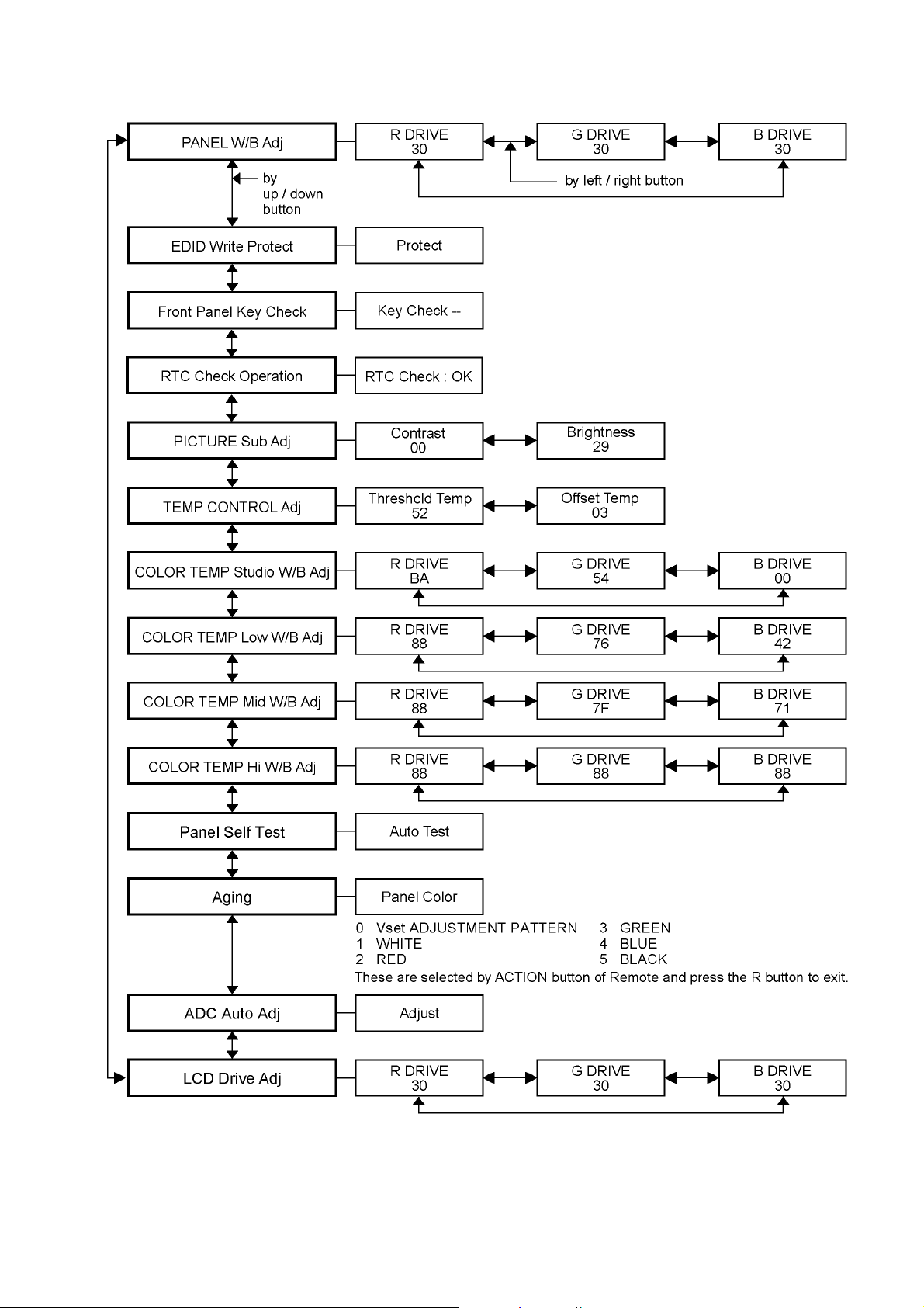
5.2. IIC mode structure (following items value is sample data)
TH-50LFE6W
13
Page 14
TH-50LFE6W
6 Troubleshooting Guide
6.1. Self Check
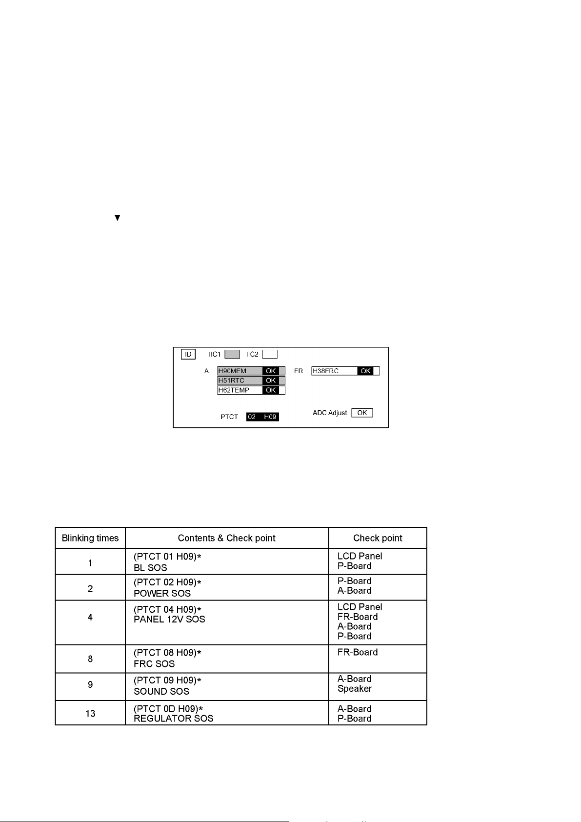
6.1.1. Display Indication
1. Self-check is used to automatically check the bus line controlled circuit of the LCD display.
2. To get into the Self-check mode, press the volume down button on the right side of the unit, at the same time pressing the
OFF-TIMER button on the remote control, and the screen will show.
Method A Self-check only (A shipment setup is not carried out).
• Select the ID mode by Up/Down button on the remote control at the front page of CAT mode and then press the Mute button
on the remote control more than 3 seconds.
Method B Self-check+Shipment setup
• Press and hold the button on the right side of the unit and press the OFF-TIMER button on the remote control.
If the IIC ports have been checked and found to be incorrect
Or not located then “ - - ” will appear in place of “ OK ”
“ 02 ” in the line of the “ PTCT ” means the number of blinks of the Power LED is 2. (Reference to 6.1.2)
“ H09 ” in the line of the “ PTCT ” is the error code.
To exit the CAT mode switch off the main power.
Note:
The line of the “ PTCT ” displays when you get into the Self-check mode for the first time only after the Power LED blinks.
6.1.2. Power LED Blinking timing chart
1. Subject
Information of LED Blinking timing chart.
2. Contents
When an abnormality has occurred to the unit, the protection circuit operates and resets to the stand by mode. At this time,
the defective block can be identified by the number of blinks of the Power LED on the front panel of the unit.
* Refer to 6.1.1 Display Indication
14
Page 15
6.1.3. LCD Panel test mode
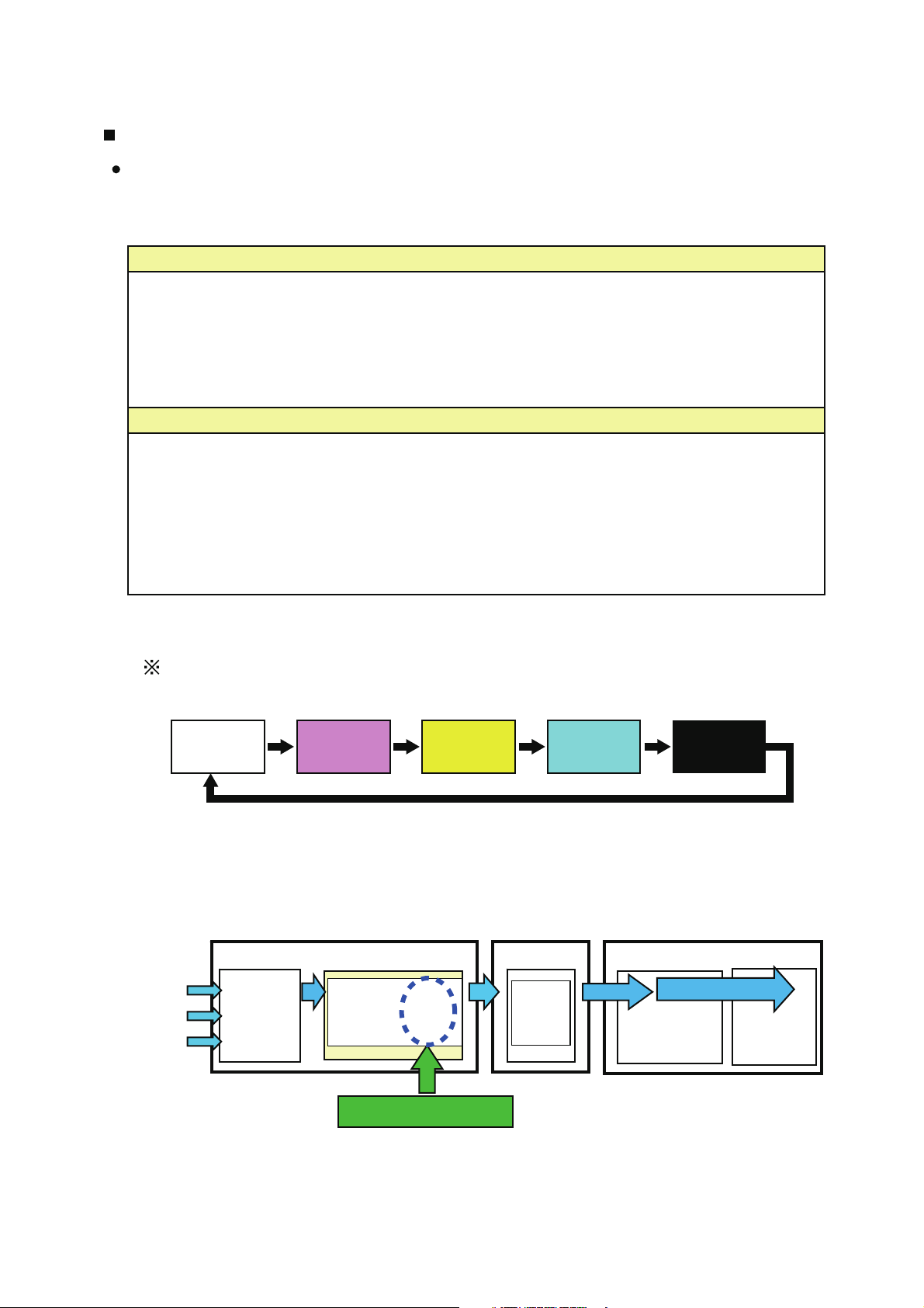
The failure-diagnosis by LCD Panel test mode
To find the possible failure point where in LCD Panel or Printed Circuit Board when the
abnormal picture is displayed.
[How to display the test pattern]
(1) Main unit + remote control operation
1. While pressing [VOLUME ( - )] button of the main unit, press [R] button of the
remote control three times within 2 seconds.
2. Test pattern is displayed and Power LED lights red and orange alternately.
How to Exit: Turn off the unit.
(2) Remote control operation only
1. Press [Recall] button of the remote control.
2. Press [R] button of the remote control.
3. Press [N] button of the remote control for over 3 seconds.
4. Test pattern is displayed and Power LED lights red and orange alternately.
TH-50LFE6W
How to Exit: The unit automatically turns off after around 10 seconds.
[Display pattern]
It is unfixed from which color it starts.
White Magenta Yellow Cyan Black
[Test pattern output image]
A-Board
IC
Input
switching
Video signal processing
IP conversion
OSD synthesis
FR-Board
IC
Doublespeed
processing
LCD Panel
T-CON
Test pattern
LCD
Test pattern
Output test pattern from A-Board
15
Page 16
TH-50LFE6W
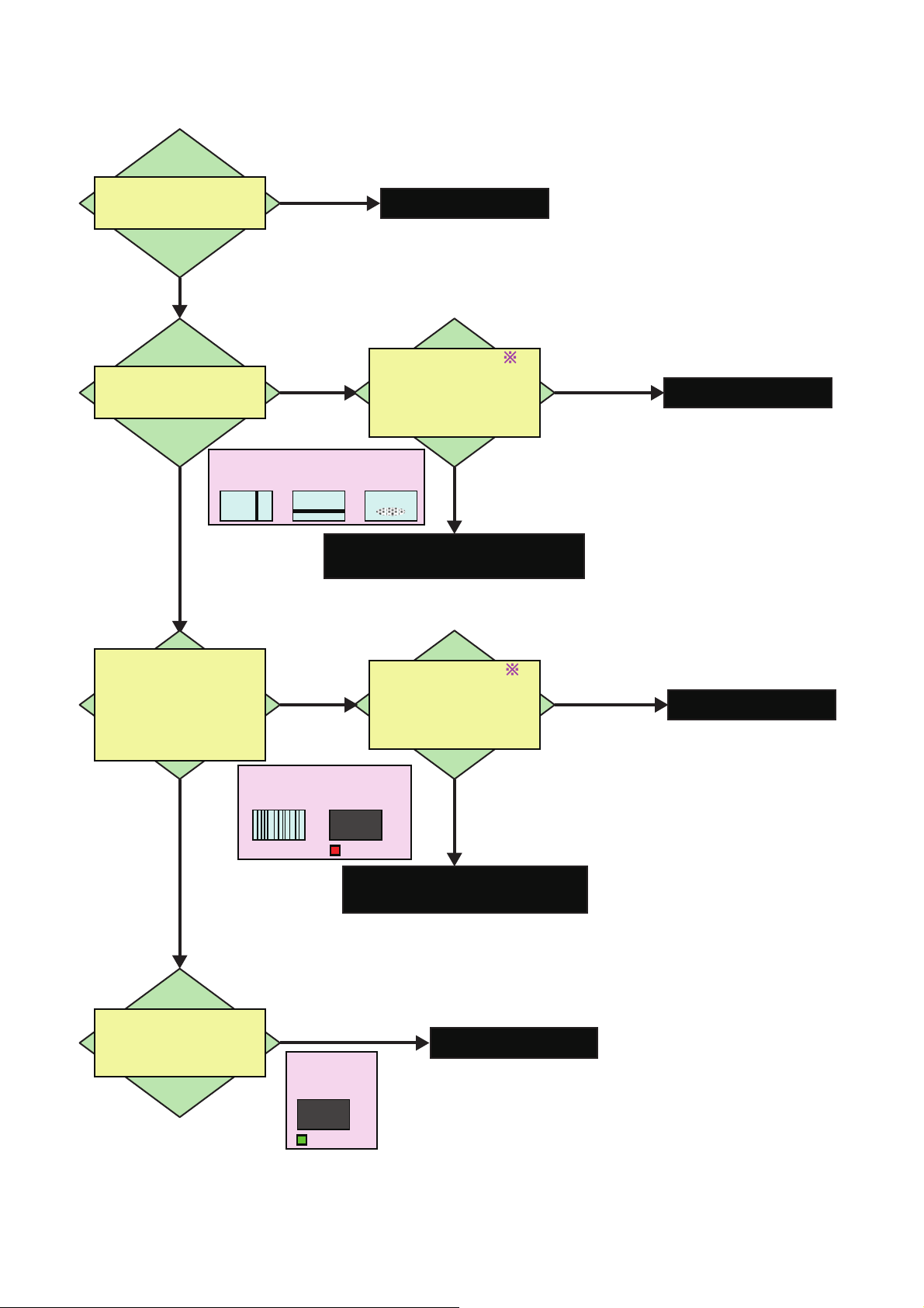
[Diagnostic flow chart]
Is a test pattern
displayed normally?
Yes
It displays.
Failure of A-Board
No
It is still abnormal.
Is a part abnormal
even in a test pattern?
Vertical line/
Vertical bar
No
This is not an abnormality
of part
Is the whole abnormal
even in a test pattern?
or
A test pattern is not
displayed but is the state
of LED blink of red and
orange?
Vertical line/
Vertical bar
Yes
It is abnormal.
Horizontal line/
Horizontal bar
Failure of LCD Panel
(rarely failure of A-Board or FR-Board)
Yes
It is abnormal.
Yes
It is blinking.
An image is
not displayed.
If "FRAME CREATION" of
"PICTURE" in On-Screen
Menu is set to "OFF", does
symptom disappear?
Color
unevenness
No
It is still abnormal.
If "FRAME CREATION" of
"PICTURE" in On-Screen
Menu is set to "OFF", does
symptom disappear?
No
It is still abnormal.
Yes
It disappears.
Failure of FR-Board
Yes
It disappears.
Failure of FR-Board
No
- The whole is not abnormal.
- It is not blinking.
A test pattern is not
displayed but is the state
of LED green lighting?
LED blinking
Failure of A-Board or LCD Panel
(rarely failure of FR-Board)
Yes
It is green lighting.
Failure of A-Board
An image is
not displayed.
Please refer to the next page for "FRAME CREATION".
LED lighting
16
Page 17
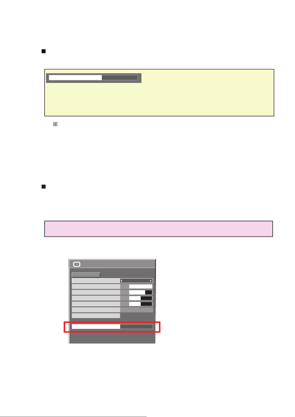
[Reference: FRAME CREATION]
FRAME CREATION is the function to double the number of display segments of an image and
to show a fast moving scene more finely.
TH-50LFE6W
FRAME CREATION
MAX
OFF :Please select "OFF", when an image is unnatural.
MIN
MIDDLE
MAX
"FRAME CREATION" setting is a setting of intermediate frame generation when
carrying out double-speed processing (from 60 to 120 frames).
Even if it sets to "OFF", it is not a function which becomes uniform processing.
-
The mode is memorized per input terminal.
-
Even if “NORMALIZE” is selected, the NORMAL setting will not be restored.
-
The picture and menu will disappear for a moment if you switch the mode to OFF, or
switch from OFF to another mode.
Setting procedure and Diagnosis when the failure-diagnosis
[1] Press [PICTURE] button of the remote control, and display "PICTURE" menu screen.
[2] Change the item of "FRAME CREATION" into "OFF".
Please check the symptoms when it is changed to "OFF".
When changing to "OFF", the normal screen is displayed: Failure of FR-Board
“PICTURE” menu screen
PICTURE
NORMALIZE
PICTURE MENU
BACKLIGHT
PICTURE
BRIGHTNESS
SHARPNESS
COLOR TEMP
ADVANCED SETTINGS
FRAME CREATION
NORMAL
STANDARD
100
70
50
50
NORMAL
MAX
17
Page 18
TH-50LFE6W
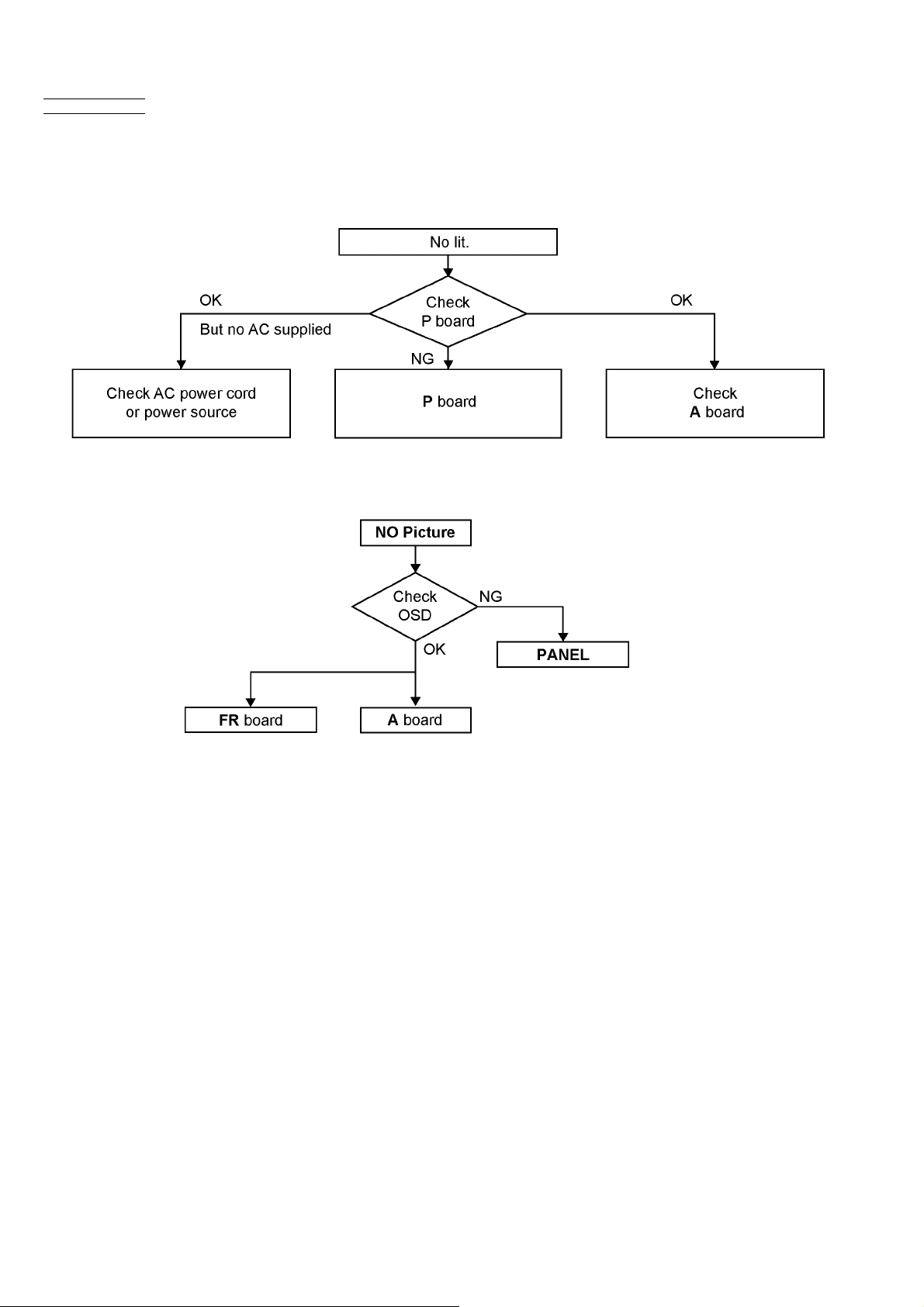
6.2. No Power
First check point
There are following 3 states of No Power indication by power LED.
1. No lit.
2. Green is lit then turns red blinking a few seconds later.
3. Only red is lit.
6.3. No Picture
18
Page 19
7 Disassembly and Assembly Instructions
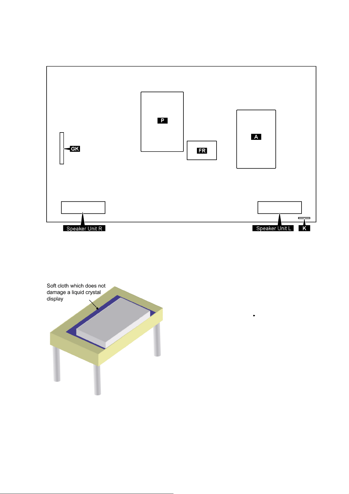
7.1. PCB Layout
TH-50LFE6W
7.2. Preparation
Please pull soft cloth etc. not to damage a screen and please
turn the front of a main part down and lay it down
7.3. About disassembly and replacement
Cautions when replacing each component
• When you replace each component, please be sure to carry
out according to the following procedure.
• When you attach each module, please do not bolt a screw
strongly.
• The part without the statement of tightening torque, please
tighten a screw 50 - 70 [N cm].
• To disassemble P.C.B., wait for 1 minute after power was off
for discharge from electrolysis capacitors.
• When tightening a screw, retention structures are required
not to deform the LCD Panel.
• Please remove a clamper and a wire processing tape if
needed in the repaire.
• Hold the specified parts to stand the monitor up. (Prevent
from the curvature and deformation of a set)
19
Page 20
TH-50LFE6W
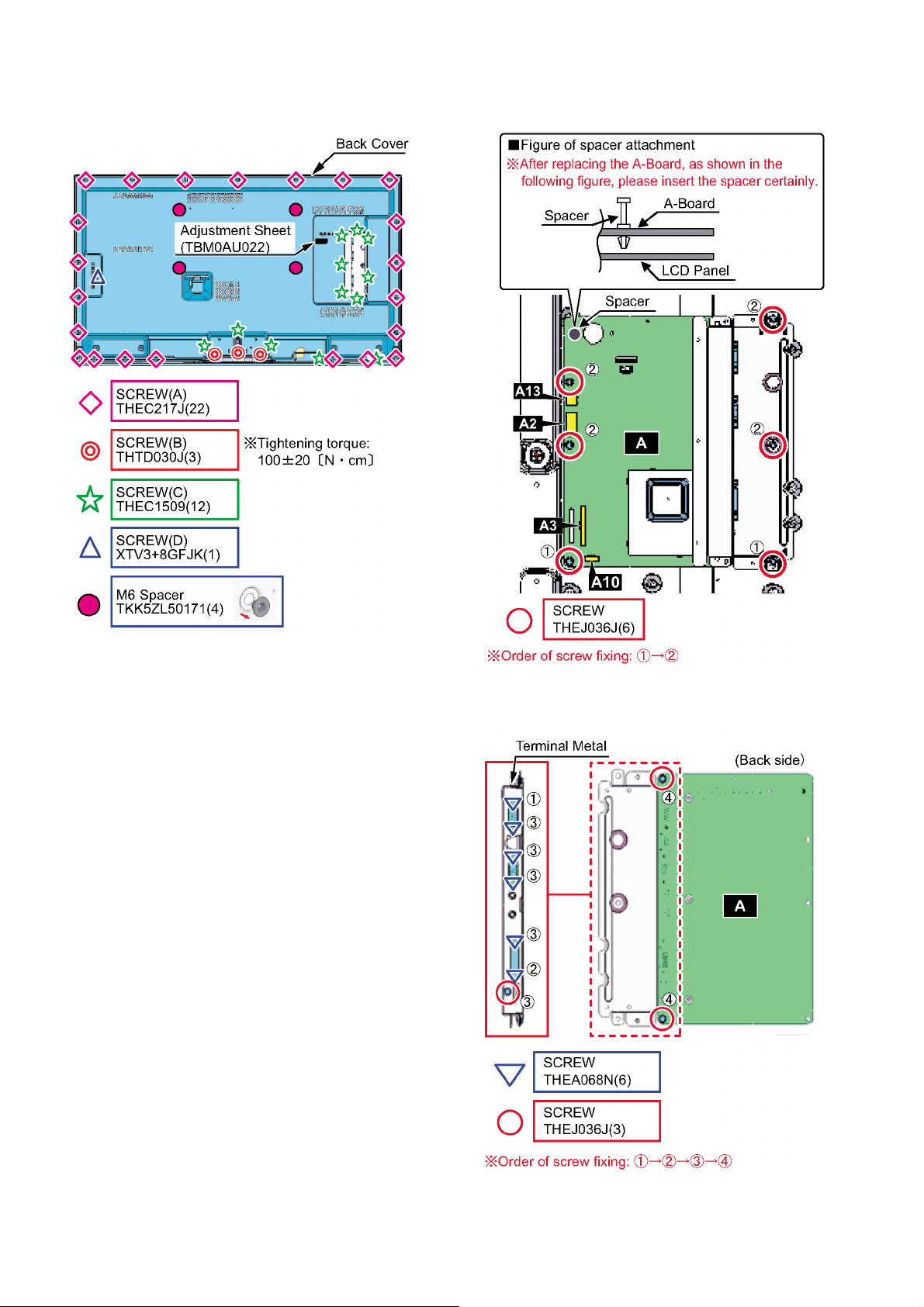
7.4. Back Cover removal
1. Remove the screws, and then remove the Back Cover.
7.5. A-Board replacement
1. Disconnect the connectors and remove the screws.
Cautions when replacing the Back Cover
• When replacing the Back Cover, please be sure to stick
the Adjutment Sheet.
2. Remove the screws, and then remove the A-Board from
the Terminal Metal.
20
Page 21
TH-50LFE6W
Caution when replacing the A-Board
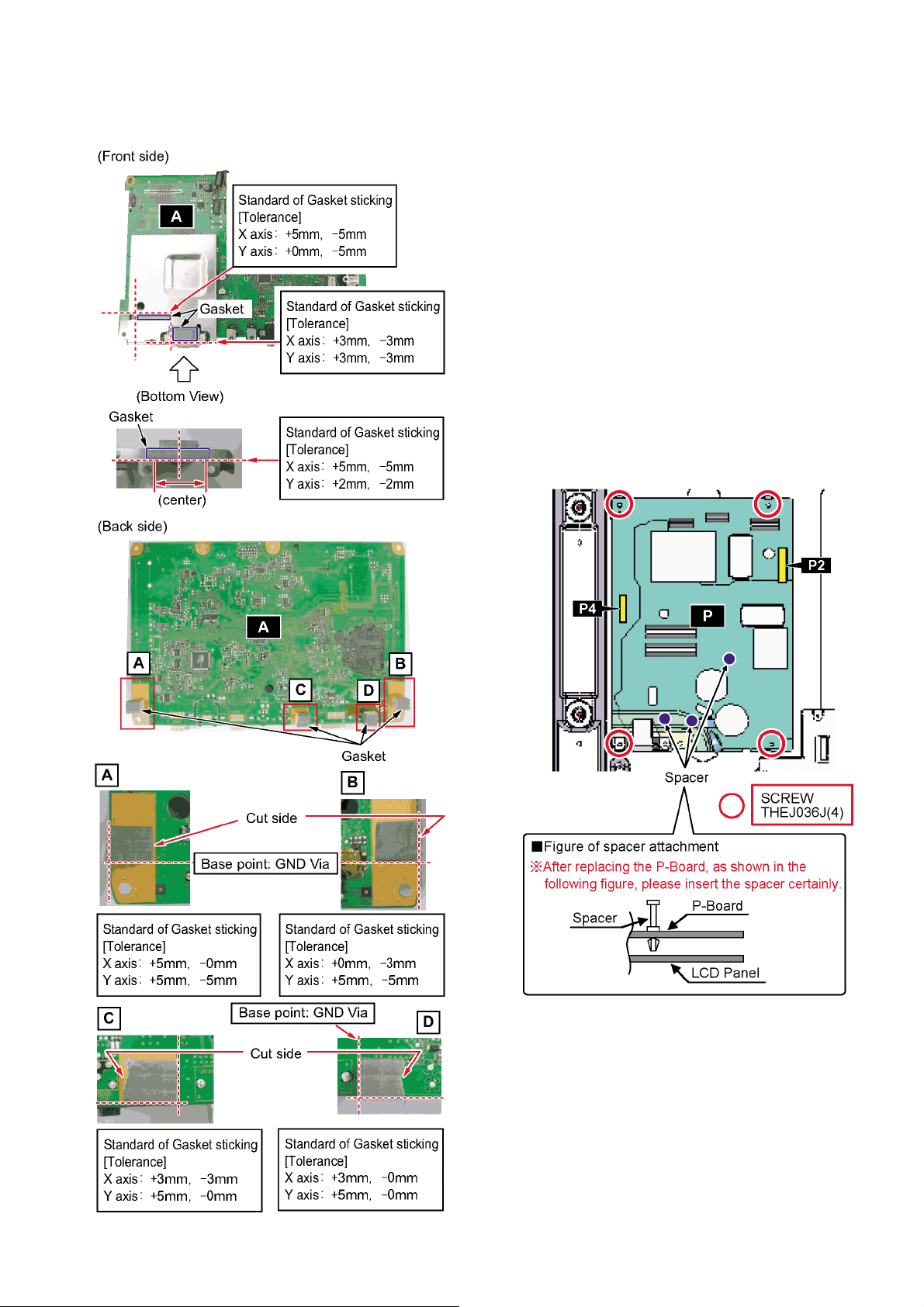
• Gaskets are enclosed in the A-Board for repaire. Please
stick the gaskets on the position of the following figure
when replacing the A-Board.
Caution after replacing the A-Board
• Since the electronic switch is adopted as a power switch
of main unit, how the rise of the power of the initial state
is different from the case of a mechanical switch in the
past.
• After replacing the A-Board, it will be in an initial state.
When you connect the AC code to a wall outlet, a power
supply state turns into a standby state, and it can turn on
the power supply of the main unit by pressing the power
button on the remote control.
* Please note that a main power supply will be in an OFF
state if a power button of main unit is pressed after connecting the AC code to a wall outlet.
Please press a power button of main unit again and turn
on the main unit.
(Since the power supply state is saved in EEPROM of ABoard, when remove/insert an AC plug, it start in the last
state after an initial state.)
7.6. P-Board replacement
1. Disconnect the connectors and remove the screws, and
then remove the P-Board.
21
Page 22
TH-50LFE6W
Caution when replacing the P-Board
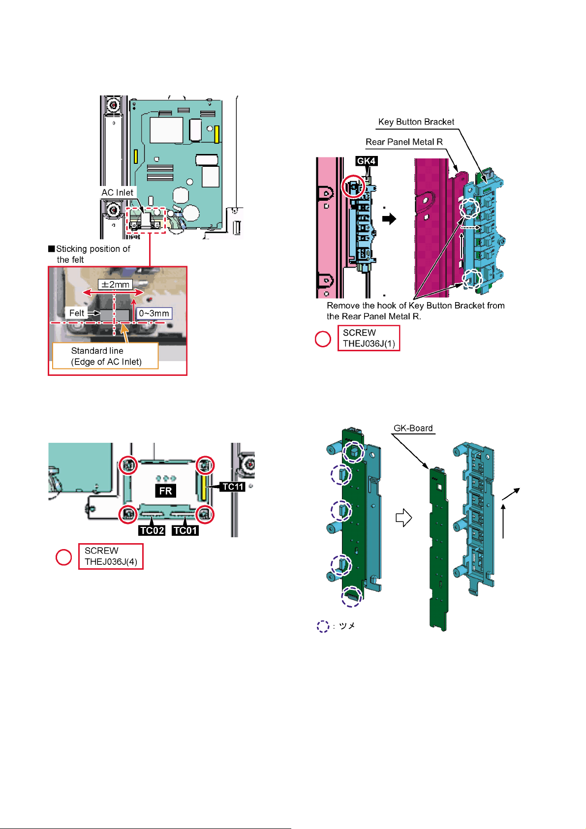
• Felt is enclosed in the P-Board for repaire. Please stick
the felt on the original position when replacing the PBoard.
7.8. GK-Board and Key Button Bracket replacement
1. Disconnect the connector and remove the screw, and
then remove the GK-Board and Key Button Bracket.
7.7. FR-Board replacement
1. Disconnect the connectors and remove the screws, and
then remove the FR-Board .
Cautions when removing/attaching the GK-Board
• When removing the GK-Board from the Key Button
Bracket, please remove it carefully to five hooks.
• The hooks are locked certainly when assembling.
22
Page 23
TH-50LFE6W
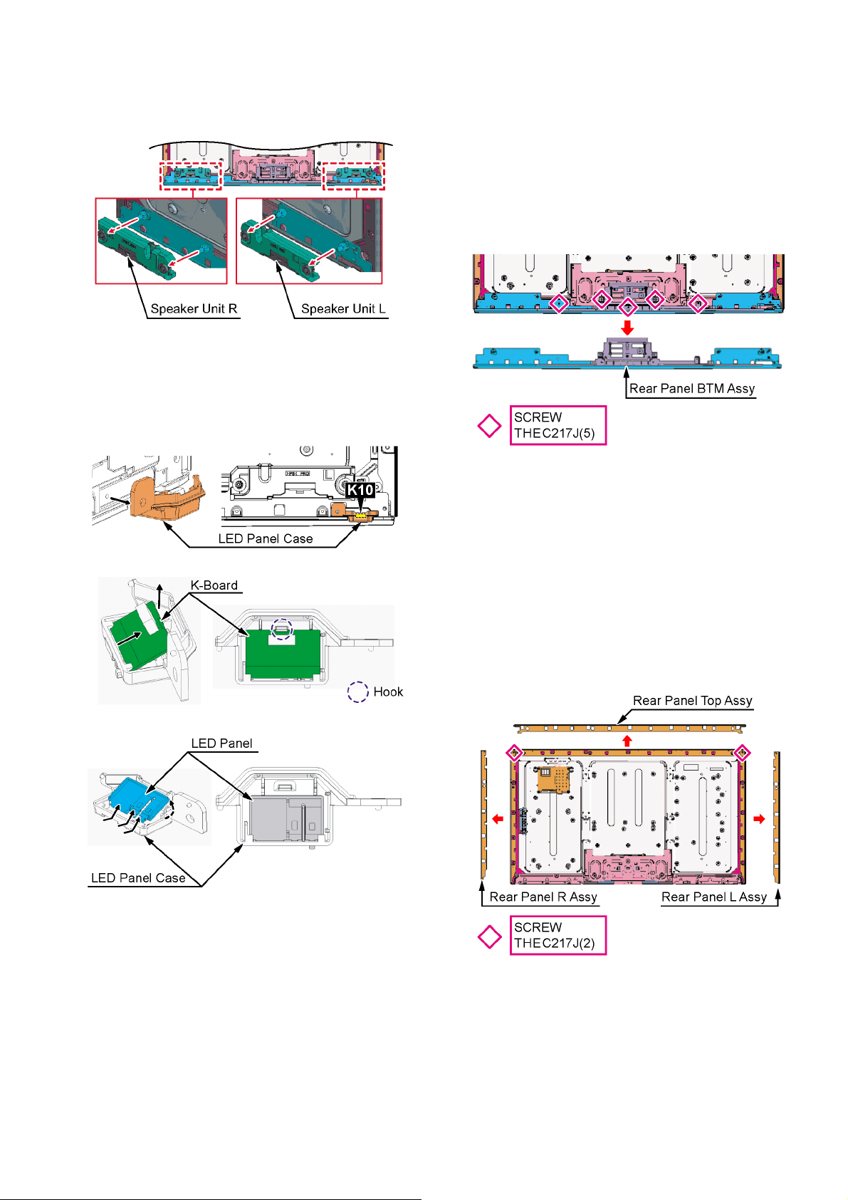
7.9. Speaker Unit L/R replacement
1. Disconnect the speaker terminal, and then remove the
Speaker Unit L/R.
7.10. K-Board, LED Panel and LED Panel Case replacement
1. Disconnect the connector, and remove the K-Board, LED
Panel and LED Panel Case.
7.11. Rear Panel BTM Assy replacement
1. Remove the Speaker Unit L/R.
(Refer to “7.9. Speaker Unit L/R replacement”)
2. Remove the LED Panel Case.
(Refer to “7.10. K-Board, LED Panel and LED Panel Case
replacement”)
3. Remove the screws, and then remove the Rear Panel
BTM Assy.
7.12. Rear Panel Top/L/R Assy replacement
1. Remove the Speaker Unit L/R.
(Refer to “7.9. Speaker Unit L/R replacement”)
2. Remove the LED Panel Case.
(Refer to “7.10. K-Board, LED Panel and LED Panel Case
replacement”)
3. Remove the Rear Panel BTM Assy.
(Refer to “7.11. Rear Panel BTM Assy replacement”)
4. Remove the screws, and then remove the Rear Panel
Top/L/R Assy.
23
Page 24
TH-50LFE6W
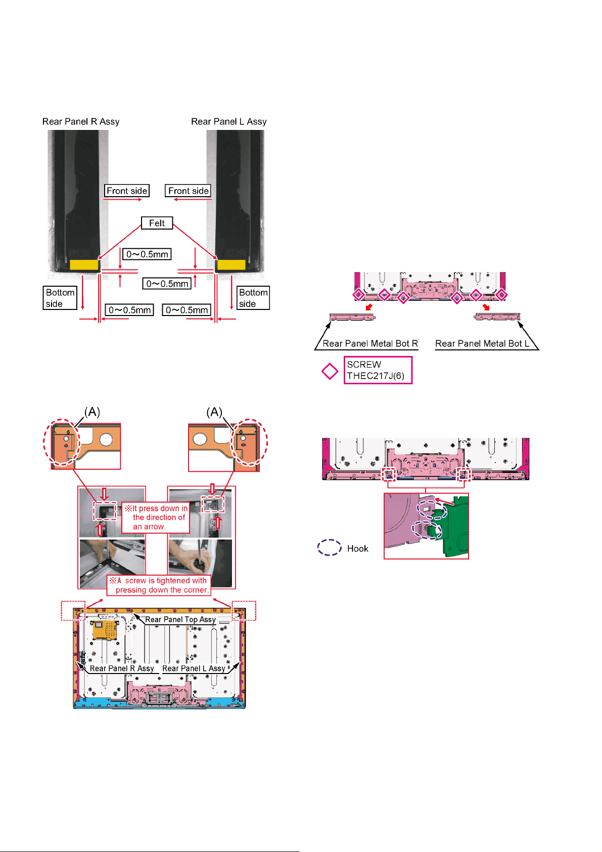
Caution when reolacing the Rear Panel L/R Assy
• Felt is enclosed in the Rear Panel L Assy and Rear
Panel R Assy for repaire. Please stick the felt on the
position of the following figure when replacing the Rear
Panel L Assy or Rear Panel R Assy.
Caution when attaching the Rear Panel Top/L/R Assy
• As shown in the following figure, please insert the part of
A correctly.
Please tighten a screw, pressing down Rear Panel L/R
Assy and Rear Panel Top Assy by hand and fixing.
7.13. Rear Panel Metal Bot L/R replacement
1. Remove the Speaker Unit L/R.
(Refer to “7.9. Speaker Unit L/R replacement”)
2. Remove the LED Panel Case.
(Refer to “7.10. K-Board, LED Panel and LED Panel Case
replacement”)
3. Remove the Rear Panel BTM Assy.
(Refer to “7.11. Rear Panel BTM Assy replacement”)
4. Remove the Rear Panel L/R Assy.
(Refer to “7.12. Rear Panel Top/L/R Assy replacement”)
• When removing the Rear Panel Metal Bot L, remove
the Rear Panel L Assy.
• When removing the Rear Panel Metal Bot R, remove
the Rear Panel R Assy.
5. Remove the screws, and then remove the Rear Panel
Metal Bot L/R.
Caution when attaching the Rear Panel Metal Bot L/R
• Please check that the hooks (positioning) of metals are
inserted firmly when assembling.
7.14. Metal Bracket Bottom replacement
1. Remove the Speaker Unit L/R.
(Refer to “7.9. Speaker Unit L/R replacement”)
2. Remove the LED Panel Case.
(Refer to “7.10. K-Board, LED Panel and LED Panel Case
replacement”)
3. Remove the Rear Panel BTM Assy.
(Refer to “7.11. Rear Panel BTM Assy replacement”)
4. Remove the Rear Panel L/R Assy.
(Refer to “7.12. Rear Panel Top/L/R Assy replacement”)
5. Remove the Rear Panel Metal Bot L/R.
(Refer to “7.13. Rear Panel Metal L/R replacement”)
24
Page 25
TH-50LFE6W
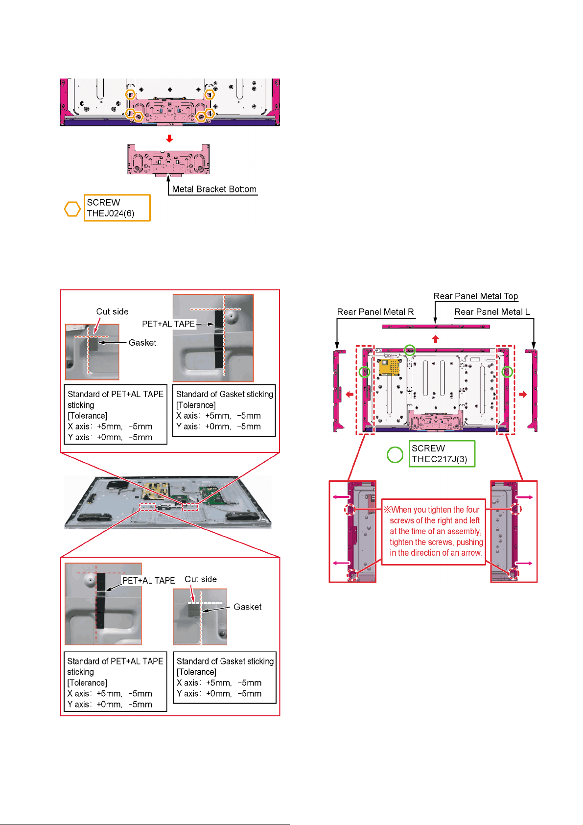
6. Remove the screws, and then remove the Metal Bracket
Bottom.
Caution when replacing the Metal Bracket Bottom
• Please stick the gaskets and PET+AL Tapes on the position of the following figure when replacing the Metal
Bracket Bottom.
7.15. Rear Panel Metal Top/L/R replacement
1. Remove the Speaker Unit L/R.
(Refer to “7.9. Speaker Unit L/R replacement”)
2. Remove the LED Panel Case.
(Refer to “7.10. K-Board, LED Panel and LED Panel Case
replacement”)
3. Remove the Rear Panel BTM Assy.
(Refer to “7.11. Rear Panel BTM Assy replacement”)
4. Remove the Rear Panel Top/L/R Assy.
(Refer to “7.12. Rear Panel Top/L/R Assy replacement”)
5. Remove the Rear Panel Metal Bot L/R.
(Refer to “7.13. Rear Panel Metal Bot L/R replacement”)
• When removing the Rear Panel Metal L, remove the
Rear Panel Metal Bot L.
• When removing the Rear Panel Metal R, remove the
Rear Panel Metal Bot R.
6. Remove the screws, and then remove the Rear Panel
Metal Top/L/R.
25
Page 26
TH-50LFE6W
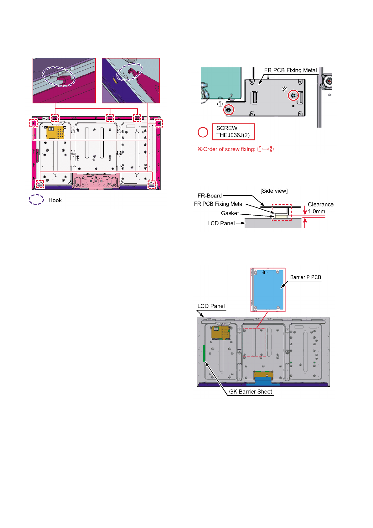
Caution when attaching the Rear Panel Metal Top/L/R
• Please check that the hooks (positioning) of metals are
inserted firmly when assembling.
11. Remove the Rear Panel Metal Top/L/R.
(Refer to “7.15. Rear Panel Metal Top/L/R replacement”)
12. Remove the screws, and then remove the FR PCB Fixing
Metal.
Cautions when replacing the FR PCB Fixing Metal
• Please tighten a screw so that the clearance between FR
PCB Fixing Metal and LCD Panel is set to 1.0 mm.
7.16. LCD Panel replacement
Caution about the sticking parts of LCD Panel
• The sticking parts for LCD Panel are enclosed.
When replacing the LCD Panel, please replace the sticking
parts simultaneously.
* Attachment specifications are subject to change without notice and parts may remain.
* Please stick on the same place as before.
Cautions about replacing the LCD Panel
• Please be sure to remove metal fittings and a clampers and
to attach them to the LCD Panel for repair. (Please check a
wiring diagram)
1. Remove the A-Board.
(Refer to “7.5. A-Board replacement”)
2. Remove the P-Board.
(Refer to “7.6. P-Board replacement”)
3. Remove the FR-Board.
(Refer to “7.7. FR-Board replacement”)
4. Remove the Key Button Bracket.
(Refer to “7.8. GK-Board and Key Button Bracket replacement”)
5. Remove the Speaker Unit L/R.
(Refer to “7.9. Speaker Unit L/R replacement”)
6. Remove the LED Panel Case.
(Refer to “7.10. K-Board, LED Panel and LED Panel Case
replacement”)
7. Remove the Rear Panel BTM Assy.
(Refer to “7.11. Rear Panel BTM Assy replacement”)
8. Remove the Rear Panel Top/L/R Assy.
(Refer to “7.12. Rear Panel Top/L/R Assy replacement”)
9. Remove the Rear Panel Metal Bot L/R.
(Refer to “7.13. Rear Panel Metal Bot L/R replacement”)
10. Remove the Metal Bracket Bottom.
(Refer to “7.14. Metal Bracket Bottom replacement”)
13. Remove the Barrier P PCB and GK Barrier Sheet.
14. Remove the flexible cable, connector and tape, and then
replace the LCD Panel.
26
Page 27
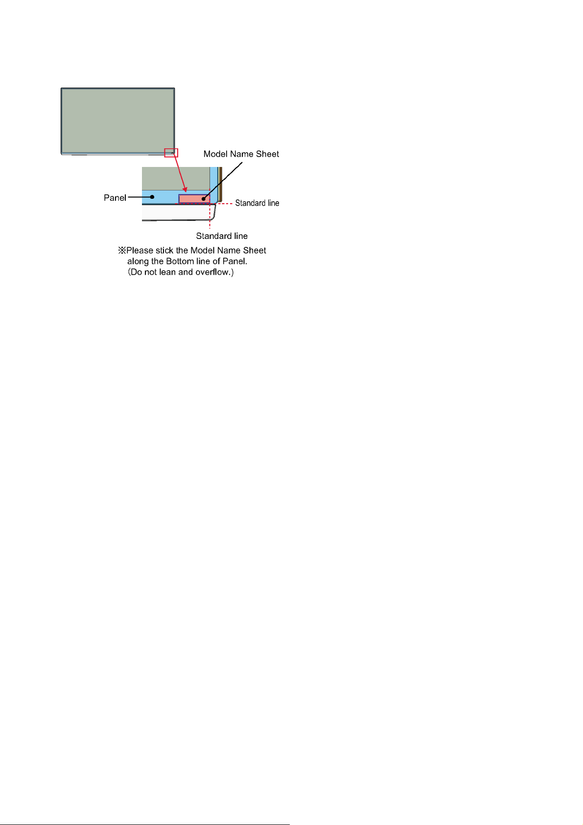
Caution when replacing the LCD Panel
• Please stick the Model Name Sheet on the position of the
following figure when replacing the LCD Panel.
About the wire arrangement after replacing the LCD Panel
• Please refer to the “Wiring Connection Diagram”.
TH-50LFE6W
Precaution when connecting the LVDS FFC
• Please insert the LVDS FFC firmly to the back.
The shortage of plugs causes failure.
27
Page 28
TH-50LFE6W
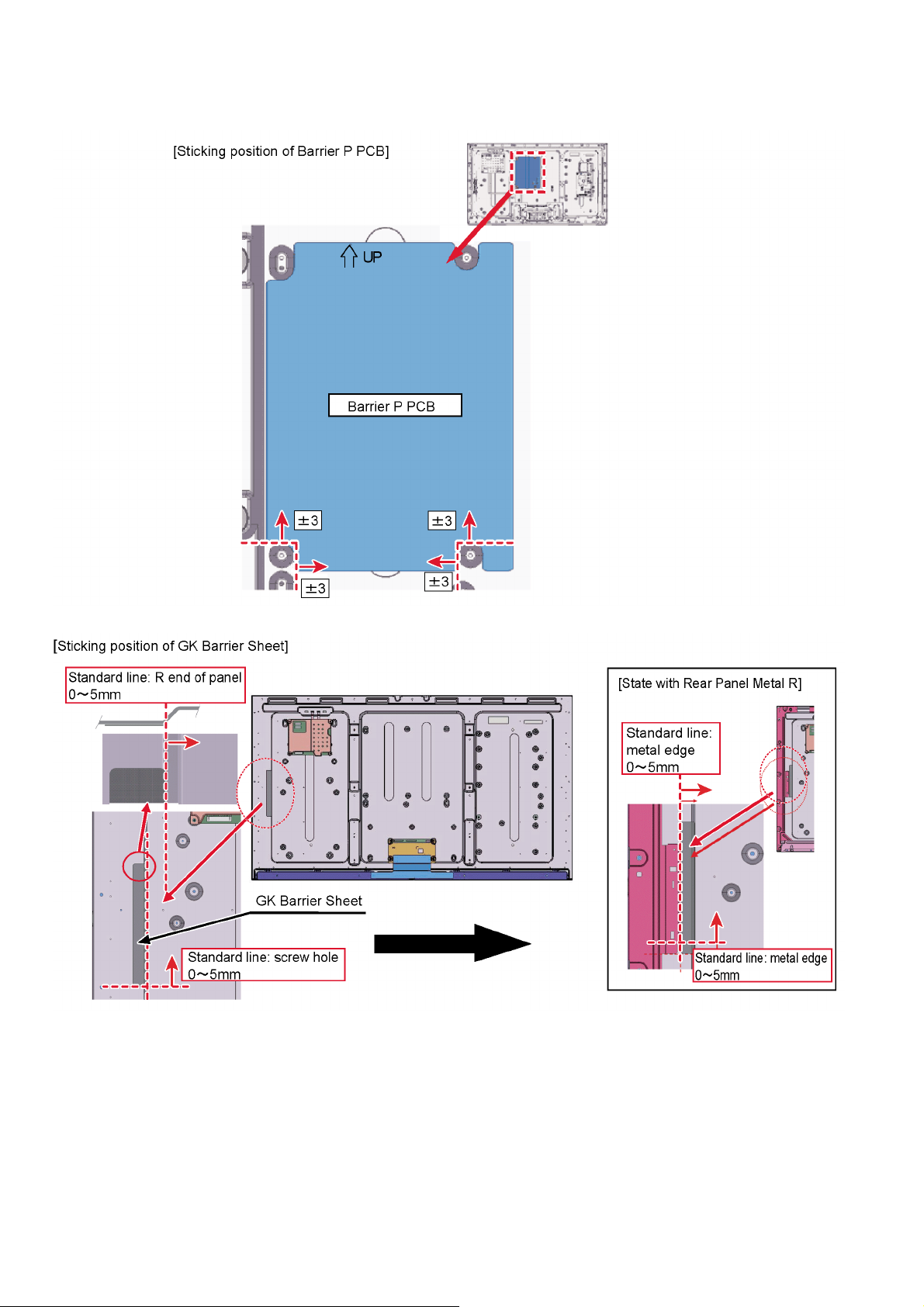
7.17. Caution about the sticking parts of LCD Panel
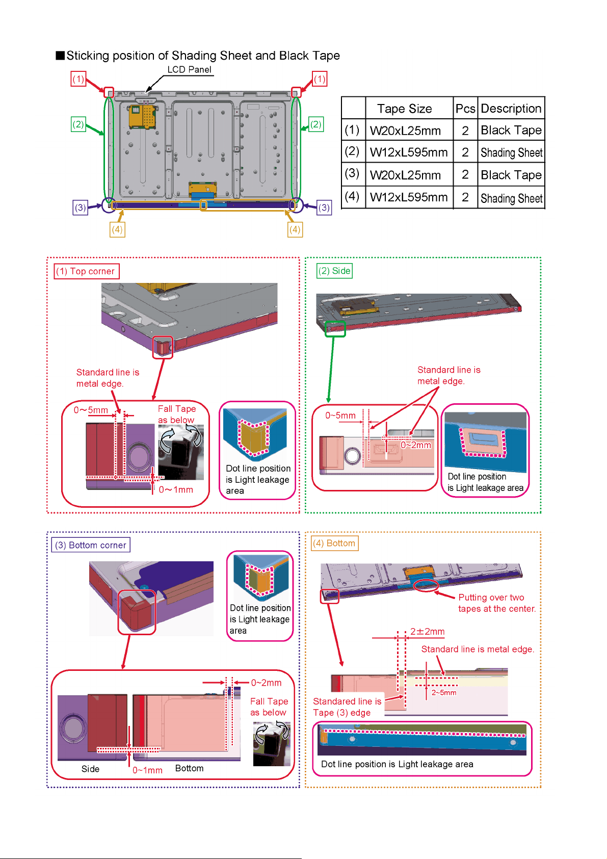
• Please remove the Barrier P PCB and GK Barrier Sheet from the old LCD Panel and stick it on the new LCD Panel for repair.
28
Page 29
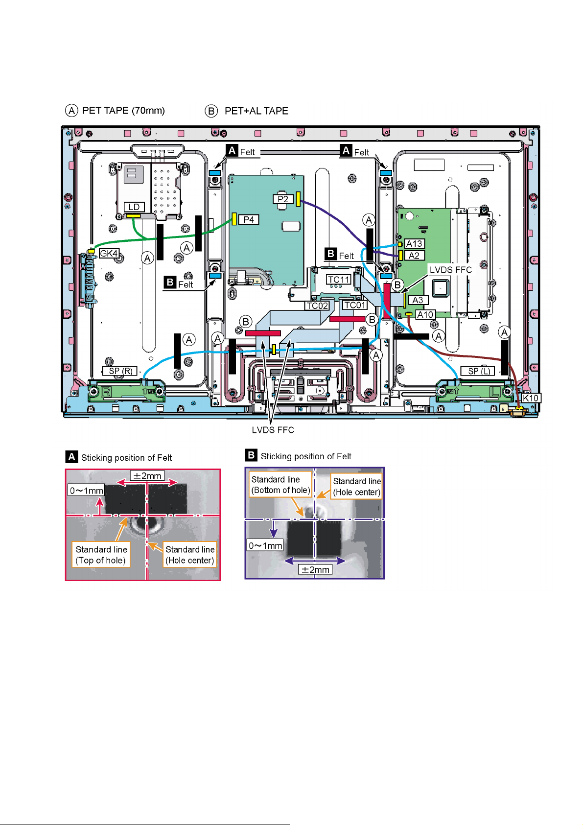
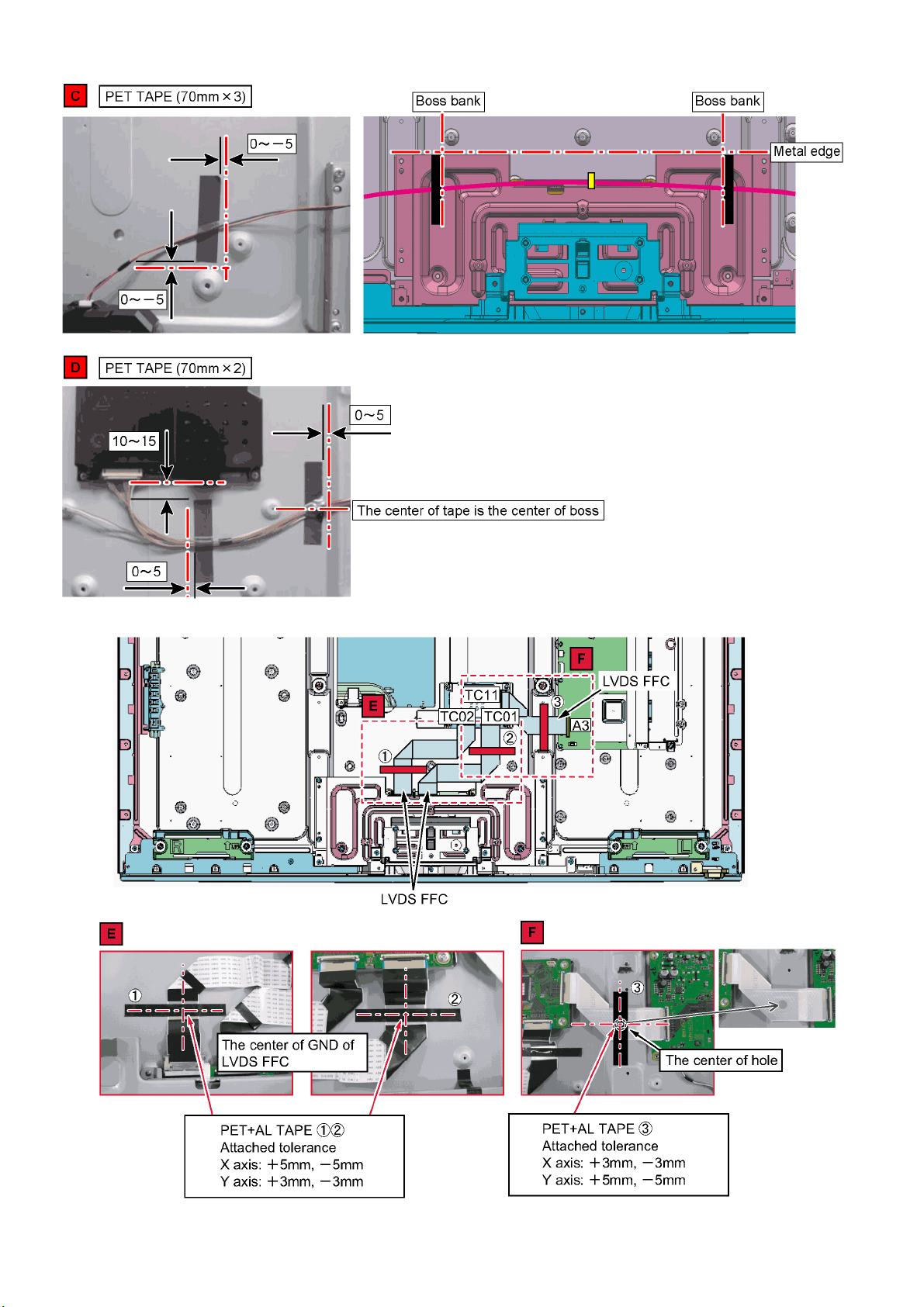
• Please stick the tapes according to the sticking position of the LCD Panel for repair after connecting the LVDS FFC.
* Attachment specifications are subject to change without notice and parts may remain.
* Please stick on the same place as before.
(Please refer to the "Wiring Connection Diagram".)
TH-50LFE6W
29
Page 30
TH-50LFE6W
30
Page 31
8 Block Diagram
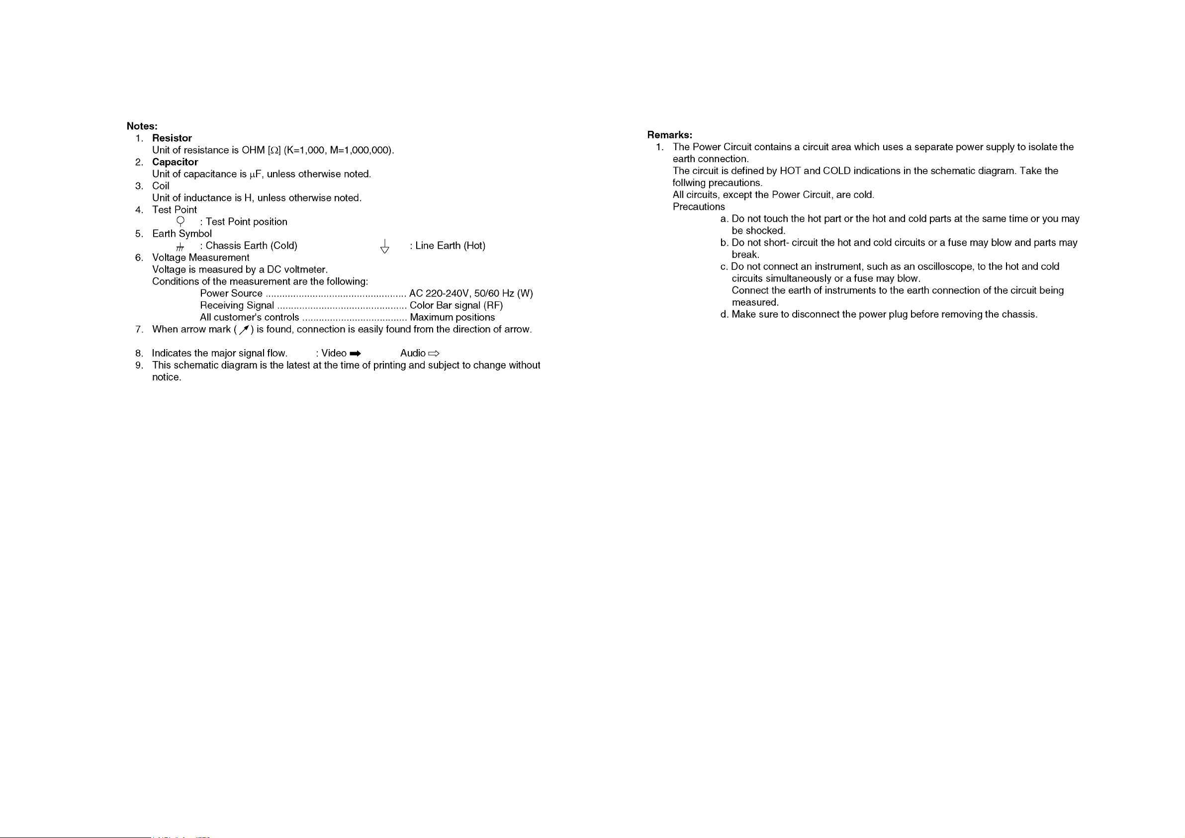
8.1. Diagram Notes
TH-50LFE6W
31
Page 32
TH-50LFE6W
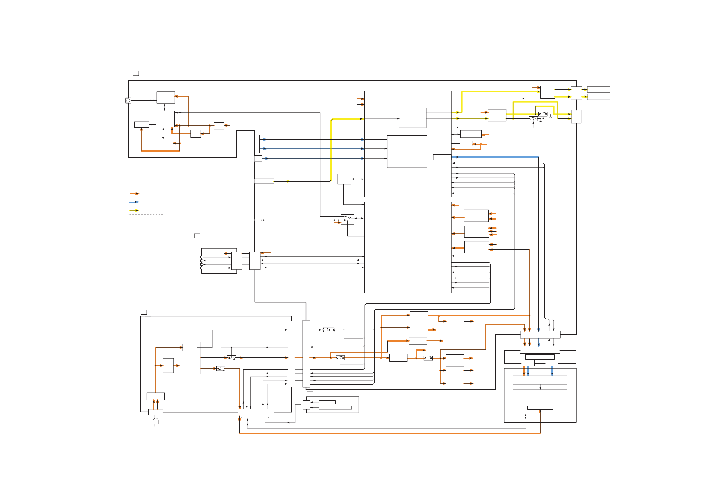
8.2. Main Block Diagram
A
DIGITAL CORE SIGNAL PROCESSOR
LAN TERMINAL
LAN DATA
EEPROM
MII DATA
POWER LINE
VIDEO LINE
AUDIO LINE
LAN
CONTROL
NETWORK
CONTROL
FLASH
MEMORY
REMOTE IN
C.A.T.S. SENSOR
DCDC
1.8V
LED_R
LED_G
K
LAN3.3V
LDO
3.3V
POWER LED
REMOTE RECEIVER
C.A.T.S. SENSOR
STB+5V/D3.3V
PWR5V
RS232C IN
K10
PC/DVI
AUDIO IN
A10
DVI
HDMI
PC
PC/DVI
R,G,B-PC
HD,VD-PC
L,R
RXD/TXD
STB+5V/D3.3V
PC/DVI AUDIO IN
STB3.3V_SW
D3.3V
D1.2V
RTC
UART SW
(LAN OR RS232C)
REMOTE
POWER LED_R
POWER LED_G
C.A.T.S.
MAIN CPU
+3.3V
+1.2V
SUB CPU
RTC_INT
RXD/TXD
UART_SW
REMOTE IN
LED_R
LED_G
C.A.T.S. SENSOR
AUDIO
PROCESSOR
VIDEO
PROCESSOR
(LED:2TIMES)
(LED:13TIMES)
PNL12V_SOS
(LED:4TIMES)
SOUND_SOS
(LED:1TIMES)
MUTE
+1.8V
LVDS
PWR_SOS
REG_SOS
BL_SOS
BL_ON
PWM1
KEY
SOUND15V
SOS DET
FRC_DONE
OEBLK
AUDIO
SERIAL AUDIO SIGNAL
+9V
LINE AMP
L/R
FLASH
MEMORY
DDR2
STB5V
+5V
PWR_SOS
(LED:2TIMES)
REG_SOS
(LED:13TIMES)
PNL12V_SOS
(LED:4TIMES)
5VD_POWER
P15V_24V_EN
DDR1.8V
MAIN_EN
LINE_OFF
P24_EN
BL_SOS
D3.3V
+9V
PANEL12V
POWER_ON
LINE_OFF
PWR5V
PWR15V
D3.3V
LAN3.3V
DDR1.8V
AMP
R
L
R+/-
L+/-
SPEAKER(R)
A13
SPEAKER(L)
LINE OUT
P
AC CORD
POWER SUPPLY
INPUT
FILTER
NEUTRAL
LIVE
JK7101
PFC
AC
DETECT
LLC
CONVERTER
PWR15V
5VD_POWER
PWR15V
P15V
DCDC
PWR5V
LINE_OFF
LINE_OFF
SUB_ON
A2
BL_SOS
P2
GK4
GK
SWITCH
P15V
POWER SW
CONTROL PANEL KEY
16V
24V
BL_PWM
BL_ON
KEY
POWER_ON
P15V24V_EN
PWR15V
MAIN_EN
BL_SOS
BL_PWM
BL_ON
POWER_ON
KEY
DCDC
PNL12V
DCDC
SOUND15V
DCDC
STB5V
PWR5V
SOUND15V
STB5V
D5V
LDO
9V
DCDC
D3.3V
DCDC
DDR1.8V
DCDC
D1.2V
+9V
D3.3V
DDR1.8V
D1.2V
PANEL12V
D5V
TC11
PIXEL WORKS
TC01
PANEL
CONTROL
PANEL
BACK LIGHT
LVDS DATA
A3
FR
DOUBLE SPEED PROCESSOR
TC02
LCD PANEL
P4
32
Page 33
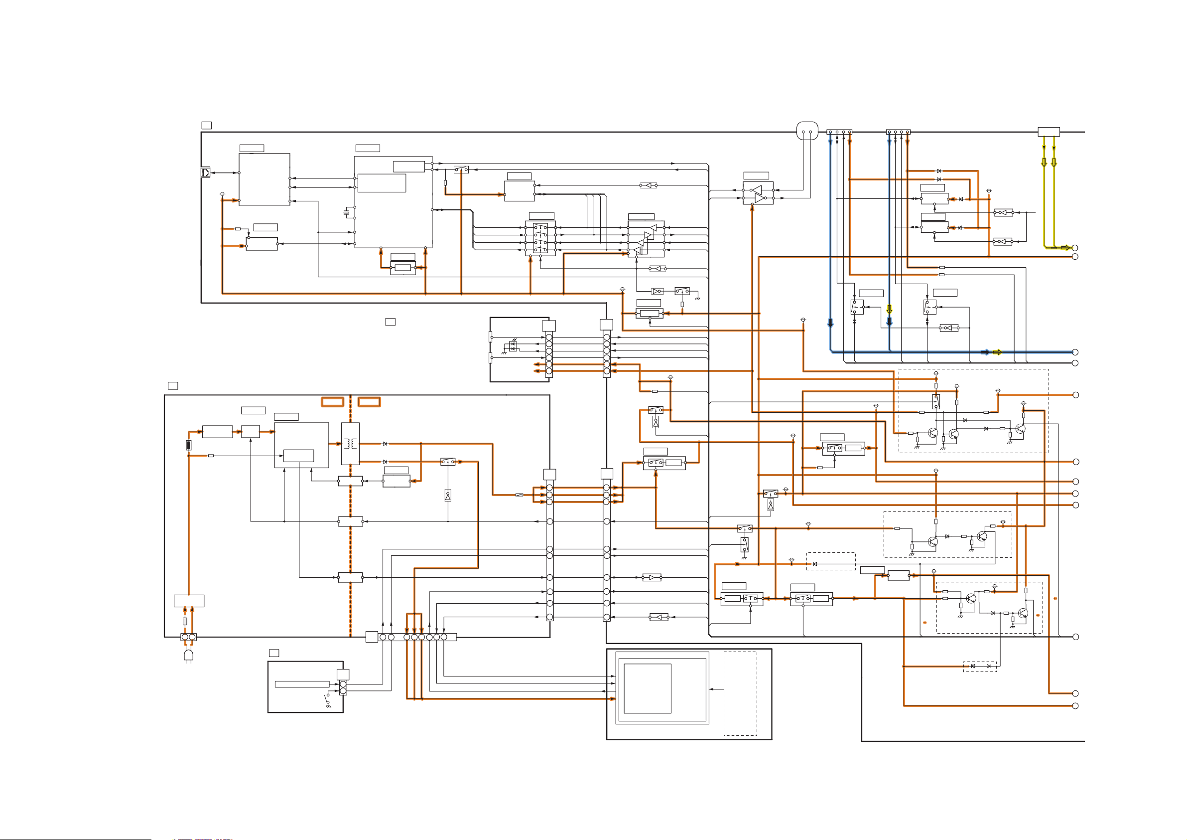
8.3. Block (1 of 3) Diagram
TH-50LFE6W
LAN TERMINAL
F7101
JK7101
AC CORD
JK2701
P
POWER SUPPLY
**
LINE
FILTER
NO
HOLDER
1
2
A
DIGITAL SIGNAL PROCESSOR
LAN
DATA
LAN3.3V
D7106
RECTIFIER
CF7103
CF7104
LF7103
LF7104
LF7105
IC2701
LAN CONTROL
+3.3V
IC2706
EEPROM
WP
VCC
IC7201
T7201,
Q7201
PFC
CLK
MII_TXD/
MII_RXD
RESET
SDA/
SCL
IC7301
LLC
CONVERTER
KEY,Power SW
GK
CONTROL PANEL KEY
CONTROL IIC
AC
DETECT
SW2851-2855
POWER SW
Q7301,
Q7302
SW2857
25MHZ
MII DATA
PC7301
PC7302
PC7303
X2701
25MHZ
HOT
T7301
PHOTO
COUPLER
PHOTO
COUPLER
PHOTO
COUPLER
GK4
2
3
IC2704
MII_MDC
MII_TXD
MII_RXD
RESET
IIC_IF
COLD
P4
D7408,9
D7401,2
12
10/100
EtherMAC
w/FIFO
+1.8V
NETWORK
CONTROLER
IC7401
TXD1
UART
RXD1
IC2703
+1.8V
POWER LED
K
REMOTE RECEIVER
C.A.T.S. SENSOR
ERROR
DETCT
+24V
+24V
8
11
9
+24V
7
+3.3V
4
3
Q7402
Q7405
1
Q2706
Q7401
SPIO_SS
SPIO_MISO
SPIO_MOSI
SPIO_SCLK
RM2800
REMOTE
RECEIVER
SN2800
C.A.T.S.
SENSOR
D2802
IC2705
SPI
FLUSH
MEMORY
REMOTE
G
R
POWER LED
PA7402
SUB_ON
KEY
POWER_ON
LINE_OFF
BL_SOS
BL_ON
BL_PWM
IC2708
EDID_WP
(IC4501)
DVI_DET
SHORT SOS
STB5V_SW
HDMI_DET
Q4094
PNL12V_SOS
JK3505
PC/DVI
AUDIO IN
PC/DVI_R
(LED 4TIMES)
PC/DVI_L
(LED 13TIMES)
REG_SOS
1
2
3
4
5
6
7
8
9
10
11
12
RS232C
DRIVER
RXD_232C
TXD_232C
JK3503
SPI_CS
SPI_SO
SPI_SI
SPI_SCK
LAN3.3V
Q2719
5V->3.3V
IC2709
Q2714,15
Q2716
RXD_LAN
TXD_LAN
SPI_LAN_WP
SPI_CS_LAN
SPI_SO_LAN
SPI_SI_LAN
SPI_SCLK_LAN
SPI_LAN_SW
NT_RST
Q2717,18
RXD_PC
TXD_PC
VCC
RS232C_IN
(SEIRIAL IN)
IC3504
IC4806
+3.3V
Q4129
Q4128
LAN3.3V_ON/OFF
LIGHT_DET
STB5V_SW
KEY_MUTE
KEY_LOCK
IR_IN
LED_G
LED_R
LAN3.3V_ON/OFF
D3.3V
A10
1
6
7
4
5
3
K10
REMOTE
1
G_LED_ON
6
R_LED_ON
7
C.A.T.S
4
STB5V_SW
5
3
LAN3.3V
STB5V
IC5201
+5V
P2
+16V
1
+16V
2
+16V
3
SUB_ON
8
KEY
10
POWER_ON
9
LINE_OFF
6
BL_SOS
11
BL_ON
12
PWM1
13
PWM1
BL_ON
STATUS
A2
D5V
1
3
5
LINE_OFF
BL_SOS
BLON_EN
KEY0
PWM1
5VD_POWER
MAIN_EN
Q5102
PWR5V
IC5102
+5V
P5V_EN
CONTROL
2
6
4
11
8
10
12
Q5201
BACK LIGHT
INVERTER
24V
CIRCUIT
P15V_24V_EN
KEY_POWER
Q4030
PANEL
Q4138
Q4602
Q5101
PWR5V
IC4904
PANEL
3
2
TXD
RXD
PWR15V
D4165
12VPAN_EN
JK4002
DVI-D IN
TMDS DATA CLOCK
IC4901
(SHORT SOS)
+12V
DDC IIC
PWR5V SOS
PANEL12V
DVI_5V
DVI_HPD
D+3.3V
+3.3V
IC4712
HDMI_I2C
D3.3V
IC4905
JK4004
HDMI IN1
DDC IIC
HDMI_5V
HDMI_HPD
HDMI DATA CLOCK
SHORT SOS
9V
PANEL12V
Q4300
Q4301
Q4088
IC4703
EEPROM
IC4706
EEPROM
HDMI_I2C
PWR_SOS
(LED 2TIMES)
IC4711
PWR5V
HDMI/DVI_SW
"L": IC4711 ON
Q4711
PWR5V
D4169
9V
Q4380,4100
SHORT SOS
D5V
D4187
Q4091,93
Q4087
D4161,64
D4400
OVP DET
PWM5V
DDR1.8V
STB5V_SW
D4174,4402
D4401
Q4024
Q4019
D5V
Q4099
33
LCD PANEL
Page 34
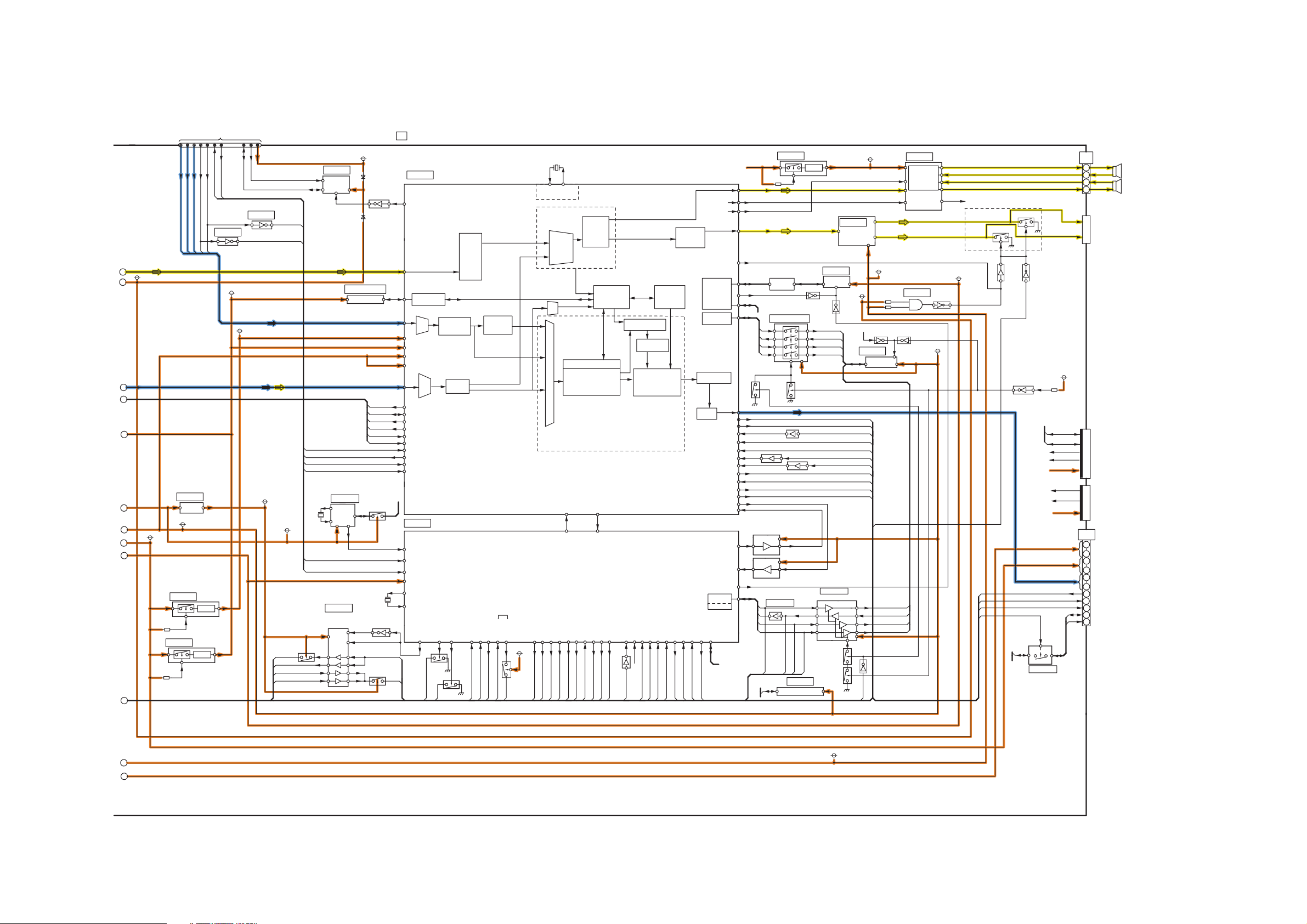
TH-50LFE6W
8.4. Block (2 of 3) Diagram
JK4001
PC
PC-R
PC-G
PC-B
V_SYNC
H_SYNC
3V_RXD3
3V_TXD3
IC4714
IC4715
VGA_-G/Y
VGA_B/PB
VGA_R/PR
1
PWR5V
2
3
4
5
IC4906
6
7
8
9
3.3V
D5V
IC4903
IC4902
10
DDR1.8V
D1.2V
STB3.3V_SW
D3.3V
D1.2V
+1.2V
DDR1.8V
+1.8V
VGA_SCL
VGA_SDA
PC_V_DET
PC_H_DET
STB5V_SW
TXD_PC
TXD_LAN
RXD_PC
RXD_LAN
X3120
PC_V_DET
PC_H_DET
LAN OR RS232C
Q2713
IC4702
EEPROM
IC4502,03
ANALOG VIDEO DATA
(R/G/B/H/V )
IC3120
REAL
TIME
CLOCK
IC2707
UART SW
3.3V
VGA_5V
Q4132
PC_DVI_L/R
DDR2
5V_I2C1
Q3120,Q3121
X4801
20MHz
Q2707
Q2712
A
DIGITAL SIGNAL PROCESSOR
IC4501
EDID_WP
DDR_SDRAM
I/F
MUX
+1.2V
+1.8V
+3.3V
AUD3.3V
MUX
HDMI/DVI_SW
HDMI_I2C
DVI_HPD
HDMI_HPD
DVI_DET
HDMI_DET
3V_RXD3
3V_TXD3
H_SYNC
V_SYNC
IC4801
RTC_INT
PC_V_DET
PC_H_DET
STB+5V
UART_SW
TXD0
Q4802
RXD0
LED_R
MAIN CPU
Analog
Capture
SUB CPU
R_LED_ON
LED_G
INPUTS
DVI/
HDMI
G_LED_ON
Q4801
SOUND15V
I2C2
RC
Q4805
Q4806
IIC2
Q4106
Q4109
I2C
5V->3V
Q4766
VCC
VCC
IC4763
SPI_CS_LAN
IC5202
5V_I2C1
Q4058
IC4761
Q4762
SPI_SW2
Q4105
Q4114
UART SW
5V->3.3V
UART SW
3.3V->5V
CS_FL
SPI_DI_S
SPI_DO_S
CLK2
SPI_SI_LAN
SPI_SO_LAN
SPI_SCLK_LAN
IC4506
TEMP SENSOR
+15V
SERIAL AUDIO SIGNAL
IC4504
EEPROM
CS#
SPI_DI
SPI_DO
SPI_CLK
SPI_SW
Q4130,31
IC4762
5V<->3.3V
Q4765
Q4763
X4004
19.6608MHz
CLOCK
GENARATION
AUDIO
PROCESSOR
DSP
AUDIO
A/D
3D VIDEO
DECORDER
TO JK3503
REMOTE
RXD0
5V_RXD
5V_TXD
TXD0
STB5V_SW
MUX
MUX
MUX
SUB_MAIN
SPI_LAN_WP
SPI_LAN_SW
LAN3.3V_ON/OFF
MOTION DETECTION
DCDI MOTION
ADAPTIVE
De-interlacing
Scaling
Shaping Filtter
MAIN_SUB2
NT_RST
POWER KEY_LOCK
KEY_POWER
P5V_EN
MEMORY
CONTROLER
VIDEO
PROCESSOR
5VD_POWER
MAIN_ON
P15V_24V_EN
2nd Channel
Processing
Enhancer ADCII
ACM-3D
3x3 Matrix
OSD Blend
SOUND_SOS
LINE_OFF
3x3
Matrix
(LED:4TIMES)
(LED:1TIMES)
BL_SOS
PNL12V_SOS
OSD
CONTROLER
(LED:13TIMES)
(LED:2TIMES)
PWR_SOS
REG_SOS
SPI_SW2
D/A
I2C_CONT
C.A.T.S_SENSOR
Q4112
IR_IN
RXD_PC
TXD_PC
Q4116
LAN3.3V_ON/OFF
SPI_LAN_WP
SPI_LAN_SW
NT_RST
P5V_EN
KEY_POWER
KEY_LOCK
5VD_POWER
MAIN_EN
P15V_24V_EN
LINE_OFF
SOUND_SOS
BL_SOS
PNL12V_SOS
PWR_SOS
REG_SOS
I2C_CONT
SPI_SW2
I2C_INT
AMP_STBY
SP_MUTE
BUS
CONTROL
SERIAL
I/F
OUTPUT
Formater
LVDS
Tx
LINE_OFF
KEYSCAN
IIC_CONT
12VPAN_EN
FRC_DONE
FLASH_WP_SUB
I2C_INT
FLASH_WP_SUB
MUTE
PWM1
BL_ON
FRC_XRST
OEBLK
3V_TXD1
3V_RXD1
5V_TXD1
5V_RXD1
WP_SUB
SERIAL
I/F
CS_FL
5V_I2C1
PWR15V
OUT_R/L
3V_I2C1
WP_MAIN
RC
SOUND15V
IC2001
LINE AMP
PWR5V
Q4057
FLASH_WP_SUB
IC4505
PWM1
BLON_EN
LINE_OFF
KEY0
LIGHT_DET
IR_IN
IIC_CONT
12VPAN_EN
FRC_DONE
FRC_XRST
OEBLK
SPI_SW2
SP_MUTE
SLEEPN
9V
Q4118
SERIAL
FLASH
KEY_MUTE
WP_SUB
Q4764
CS#
SO/SI01
SI/SI00
SCLK
Q4125
SPI_SW2
IC5103
AUDIO
OUT
AUDIO AMP
IC2002
SPI_SW
D3.3V
SPI_SW
Q2042
STB5V
SOUND_SOS(IC4801)
LINE MUTE
Q2052
Q2054
Q2051
Q4761
12VPAN_EN
IIC2
Q2053
PANEL12V
D5V
LVDS DATA
FRC_DONE
FRS_XRST
OEBLK
IC4509
R(+)
R(-)
L(-)
L(+)
SPI_SW
D3.3V
5V_I2C1
5V_I2C2
I2C_INT
I2C_CONT
STB5V
STB5V
R OUT
L OUT
MODE
RESET
A13
1
2
3
4
A3
1
9
11
13
19
47
51
52
58
54
55
JK3506
LINE OUT
A40
FOR
FACTORY
USE
A48
FOR
FACTORY
USE
TO FR-BOARD
(TC11)
SPEAKER_R
SPEAKER_L
9V
11
12
9V
34
Page 35
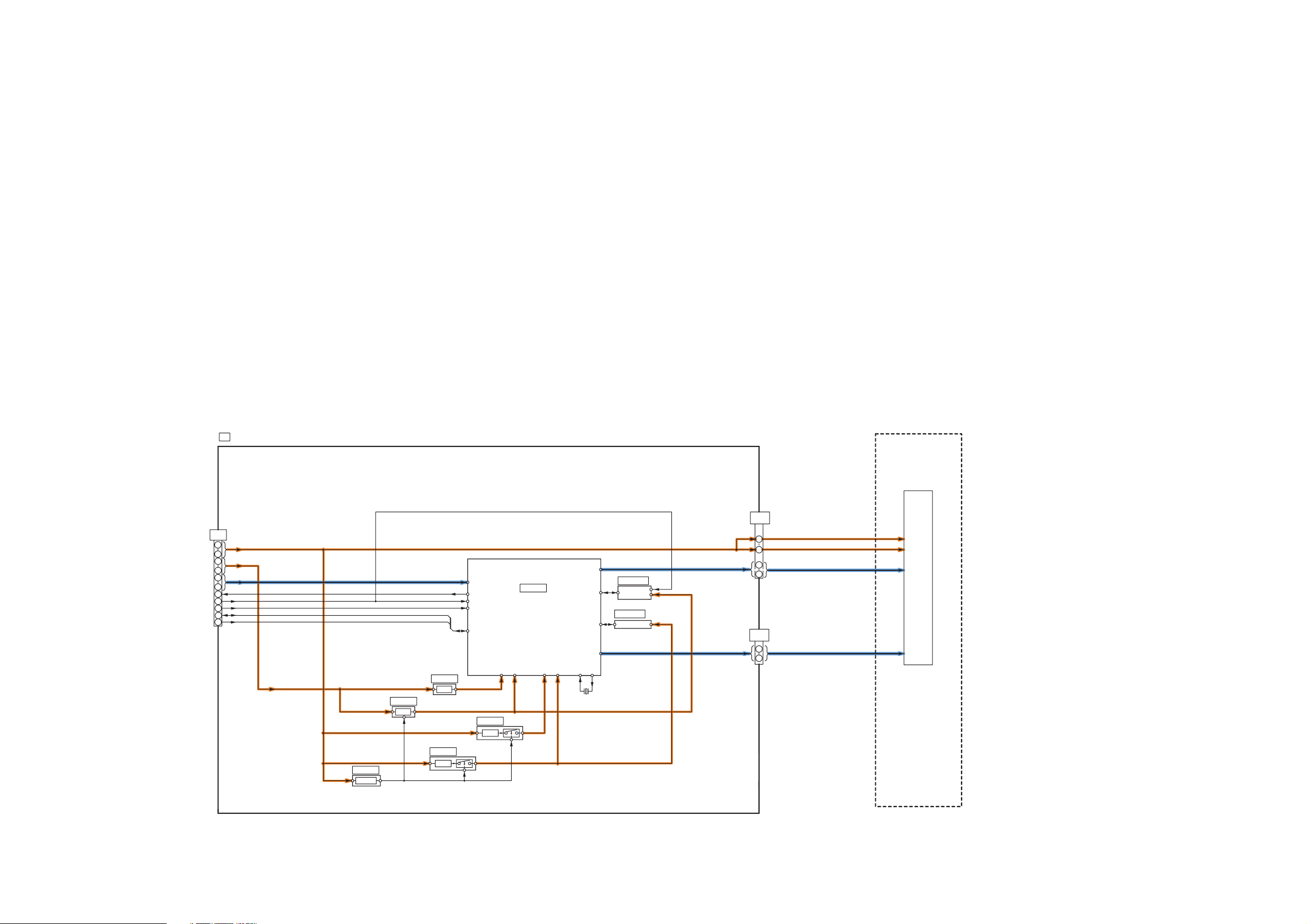
8.5. Block (3 of 3) Diagram
TH-50LFE6W
TO A-BOARD
(A3)
FR
DOUBLE SPEED PROCESSOR
TC11
60
52
50
48
42
14
10
9
5
7
6
PANEL+12V
LVDS DATA
FRC_DONE
FRC_XRST
OEBLK
SUB5V
IC9300
DCDCEN
IC9351
+3.3V
DCDCEN
IC9303
+2.5V
IC9302
+1.8V
FRC_DONE
RESETN
OEBLK
I2C(TCON_12C)
IC9301
+1.0V
PIXCEL WORKS
PNL3.3V
FRC+2.5V
IC9100
(FRC)
FRC+1.0V
FRC+1.8V
SPI I/F
DDR I/F
X9100
LCD PANEL
TC01
PANEL+12V
1
4
11
LVDS DATA
IC9350
SPI
FLASH
40
LCD PANEL
CONTROL
IC9250
DDR
TC02
3
LVDS DATA
32
XIN
XOUT
35
Page 36

TH-50LFE6W
36
Page 37
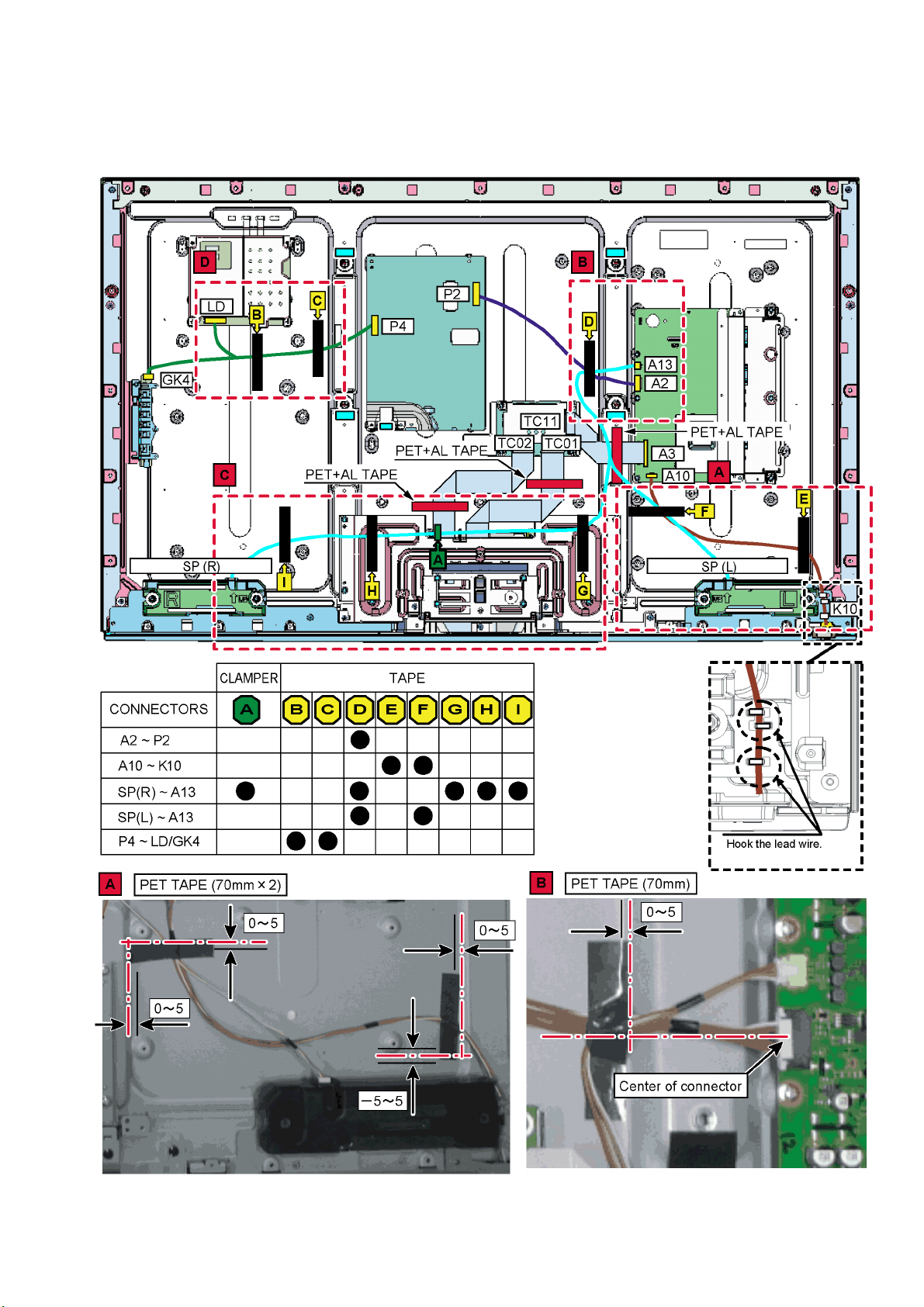
9 Wiring Connection Diagram
9.1. Wiring Connection Diagram
TH-50LFE6W
37
Page 38
TH-50LFE6W
38
 Loading...