

Page 1
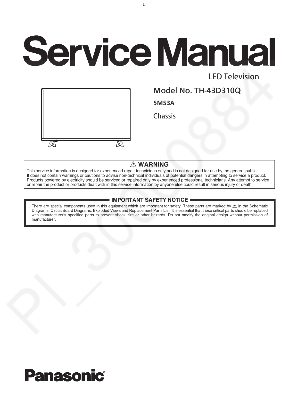
Model No. TH-43D310Q
1
5M53A
Chassis
LED Television
Page 2
SCHNEIDER ELECTRONICS GMBH-GERMANY
2
1. CAUTION
CAUTION:
Use of controls, adjustments or procedures other than those specified herein may result in
hazardous radiation exposure.
CA UT ION : TO RE DU CE THE RIS K OF
CAU T ION
RISK OF ELECTRI C
SHOCK DO NOT OPEN.
The lighting flash with arrowhead symbol, with an equilateral triangle is intended to
alert the user to the presence of uninsulated voltage within the products
enclosure that may be of sufficient magnitude to constitute a risk of electric shock to
the person.
The exclamation point within an equilateral triangle is intended to alert the user to the
presence of important operating and maintenance (servicing) instructions in the
literature accompanying the appliance.
ELECTR ICAL SHOCK, DO NOT REMOVE
COVER (OR BACK). NO USER SERVIC EABLE
PAR TS INS IDE. RE FE R SER VIC ING TO
QUALIFIE D SERVICE PERSONNEL.
dangerous
WARNING: TO REDUCE RISK OF FIRE OR ELECTRIC SHOCK, DO
NOT
EXPOSE THIS APPLIANCE TO RAIN OR MOISTURE.
2
Page 3

SCHNEIDER ELECTRONICS GMBH-GERMANY
3
IMPORTANT SAFETY INSTRUCTIONS
CAUTION:
Read all of these instructions. Save these instructions for later use. Foll ow all W arnings and
Instructions marked on the audio equipment.
1. Read Instructions-All the safety and operating instructionsshouldbe read beforethe productis operated.
2. Retain Instructions- The safety and operating instructions should be retained for future reference.
3. Heed Warnings- All warnings on the product and in the operating instructions should be adhered to.
4. Follow Instructions- All operating and use instructions should be followed.
FOR YOUR PERSONAL SAFETY
1. When the power cord or plug is damaged or frayed, unplug this television set from the wall outlet and refer servicing to
qualified service personnel.
2. Do not overload wall outlets and extension cords as this can result in fire or electric shock.
3. Do not allow anything to rest on or roll over the power cord, and do not place the TV where power cord is subject to
traffic or abuse. This may result in a shock or fire hazard.
4. Do not attempt to service this television set yourself as opening or removing covers may expose you to dangerous
voltage or other hazards. Refer all servicing to qualified service personnel.
5. Never push objects of any kind into this television set through cabinet slots as they may touch dangerous voltage
points or short out parts that could result in a fire or electric shock. Never spill liquid of any kind on the television set.
6. If the television set has been dropped or the cabinet has been damaged, unplugthis television set from the wall outlet
and refer servicing to qualified service personnel.
7. If liquid has been spilled into the television set, unplug this television set from the wall outlet and refer servicing to
qualified service personnel.
8. Do not subject your television set to impact of any kind. Be particularly careful not to damage the picture tube surface.
9. Unplug this television set from the wall outlet bef
damp cloth for cleaning.
10.1. Do not place this television set on an unstable cart, stand, or table. The television set may fall, causing serious injury
to a child or an adult, and serious damage to the appliance. Use only with a cart or stand recommended by the
manufacturer, or sold with the television set. Wall or shelf mounting should follow the manufacturer s instructions, and
should use a mounting kit approved by the manufacturer.
10.2. An appliance and cart combination should be moved with care. Quick stops, excessive force, and uneven surfaces
may cause the appliance and cart combination to overturn.
ore cleaning. Do not use liquid cleaners or aerosol cleaners. Use a
3
Page 4
SCHNEIDER ELECTRONICS GMBH-GERMANY
4
PROTECTION AND LOCATION OF YOUR SET
11. Do not use this television set near water ... for example, near a bathtub, washbowl, kitchen sink, or laundry tub, in a
wet basement, or near a swimming pool, etc.
Never expose the set to rain or water. If the set has been exposed to rain or water, unplug the set from the wall
outlet and refer servicing to qualified service personnel.
12. Choose a place where light (artificial or sunlight) does not shine directly on the screen.
13. Avoid dusty places, since piling up of dust inside TV chassis may cause failure of the set when high humidity persists.
14. The set has slots, or openings in the cabinet for ventilation purposes, to provide reliable operation of the receiver, to
protect it from o
verheating. These openings must not be blocked or covered.
Never cover the slots or openings with cloth or other material.
Never block the bottom ventilation slots of the set by placing it on a bed, sofa, rug, etc.
Never place the set near or over a radiator or heat register.
Never place the set in enclosure, unless proper ventilation is provided.
a built-in
PROTECTION AND LOCATION OF YOUR SET
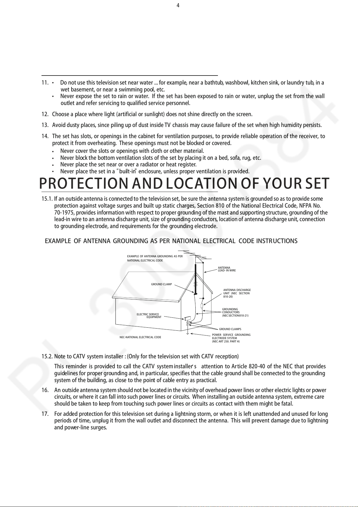
15.1. If an outside antenna is connected to the television set, be sure the antenna system is grounded so as to provide some
protection against voltage surges and built up static charges, Section 810 of the National Electrical Code, NFPA No.
70-1975, provides information with respect to proper grounding of the mast and supportingstructure, grounding of the
lead-in wire to an antenna discharge unit, size of grounding conductors, location of antenna discharge unit, connection
to grounding electrode, and requirements for the grounding electrode.
EXAMPLE OF ANTENNA GROUNDING AS PER NATIONAL ELECTRICAL CODE INSTRUCTIONS
EXAMPLE OF ANTENNA GROUNDING AS PER
NATIONAL ELECTRICAL CODE
ANTENNA
LEAD- IN WIRE
GROUND CLAMP
ELECTRIC SERVICE
EQUIPMENT
NEC-NATIONAL ELECTRICAL CODE
ANTENNA DISCHARGE
UNIT (NEC SECTION
810-20)
GROUNDING
CONDUCTORS
(NECSECTION 810-21)
GROUND CLAMPS
POWER SER VICE GROUNDING
ELECTRODE SYSTEM
(NEC ART 250. PART H)
15.2. Note to CATV system installer : (Only for the television set with CATV reception)
This reminder is provided to call the CATV system attention to Article 820-40 of the NEC that provides
installer s
guidelines for proper grounding and, in particular, specifies that the cable ground shall be connected to the grounding
system of the building, as close to the point of cable entry as practical.
16. An outside antenna system should not be located in the vicinity of overhead power lines or other electric lights or power
circuits, or where it can fall into such power lines or circuits. When installing an outside antenna system, extreme care
should be taken to keep from touching such power lines or circuits as contact with them might be fatal.
17. For added protection for this television set during a lightning storm, or when it is left unattended and unused for long
periods of
time, unplug it from the wall outlet and disconnect the antenna. This will prevent damage due to lightning
and power-line surges.
4
Page 5
SCHNEIDER ELECTRONICS GMBH-GERMANY
5
OPERATION OF YOUR SET
18.
This television set should be operated only from the type of power source indicated on the marking label.If you are not
sure of the type of power supply at your home, consult your television dealer or local power company. For television
sets designed to operate from battery power, refer to the operating instructions.
19. If the television set does not operate normally by following the operating instructions, unplugthis televisionset from the
wall outlet and refer servicing to qualifiedservice personnel. Adjust only those controls that are coveredin the operating
instructions as improper adjustment of other controls may result in damage and will often require extensive work by a
qualified technician to restore the television set to normal operation.
20. When going on a holiday : If your television set is to remain unused for a period of time, for instance, when you go on
a holiday, turn the television set and unplug the television set from the wall outlet.
off
IF THE SET DOES NOT OPERATE PROPERLY
21. If youare unable to restorenormaloperationby followingthe detailedprocedureinyouroperatinginstructions,
do not attempt any further adjustment. Unplug the set and call your dealer or service technician.
22. Whenever the television set is damaged or fails, or a distinct change in performance indicates a need for
service, unplug the set and have it checked by a professional service technician.
23. It is normal for some TV sets to make occasional snapping or popping sounds, particularly when being
turned on or off. If the snapping or popping is continuous or frequent, unplug the set and consult your
dealer or service technician.
FOR SERVICE AND MODIFICATION
24. Do not use attachments not recommendedby the television set manufacturer as they may cause hazards.
25. When replacementparts are required, be sure the service technicianhas used replacement parts specified
by the manufacturer that have the same characteristics as the original part. Unauthorized substitutions
may result in fire, electric shock, or other hazards.
26. Upon completion of any service or repairs to the television set, ask the service technician to perform
routine safety checks to determine that the television is in safe operating condition.
5
Page 6
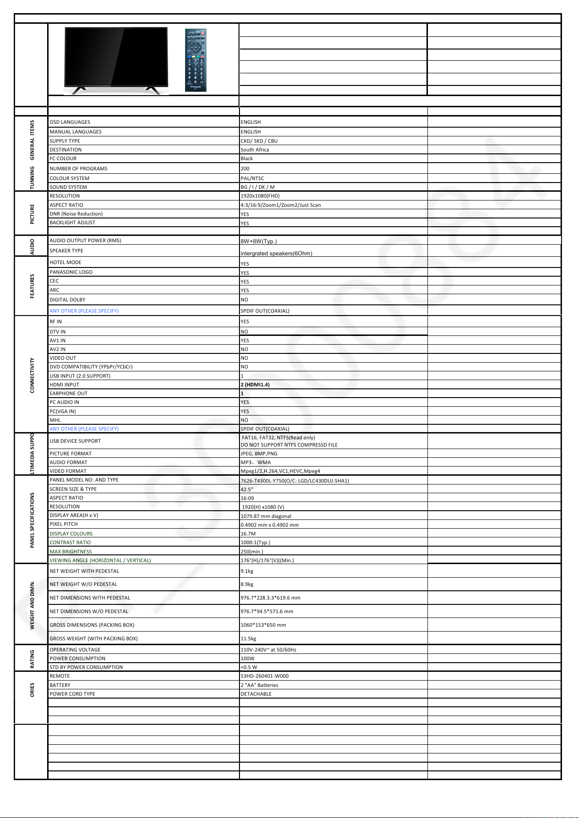
PRODUCT SPECIFIC ATIONS LED TV
ID
CATEGORY: 43" LED TV HD
MODEL NO: TH-43D310Q
REFERENCE MODE L (PANASONIC/COMPETITION): TH-43D310Q Panason ic
:
ASSEMBLER South A frica
ID PHOTO R EMOTE: Add Picture CHASSIS / Main Board:5M53A
PARAMETER S SPECIFICATIONS REMARKS (I F ANY)
GENERAL ITEM S
OSD LANGUAGES ENGLISH
MANUAL LANGUAGE S ENGLISH
SUPPLY TYP E CKD / SKD / CBU
DESTINATION South Africa
FC COLOUR Black
TUNNING
NUMBER OF PROGRAMS 200
COLOUR SYSTEM P AL/NTSC
SOUND SYSTEM BG / I / DK / M
PICTURE
RESOLUTION 1920x1080(FHD)
ASPECT RATIO 4:3/16:9/Zoom1/Zoom 2/Just Scan
DNR (Noise Reduction)
YES
BACKLIGHT ADJUST
YES
AUDIO
AUDIO OUTPUT P OWER (RMS)
8W+8W (Typ.)
SPEAKER TYP E
intergrated speakers(6Ohm)
FEATURES
HOTEL MODE
YES
PANASONIC LOGO
YES
CEC
YES
ARC
YES
DIGITAL DOLBY NO
ANY OTHER (PLE ASE SPECIFY) SPDIF OUT(COAX IAL)
CONNECTIVITY
RF IN YES
DTV IN NO
AV1 IN YES
AV2 IN NO
VIDEO OUT NO
DVD COMPATIBILITY (YPbPr/YCbCr) NO
USB INPUT (2.0 SU PPORT) 1
HDMI INPUT 2 (HDMI1.4)
EARPHONE OUT 1
PC AUDIO IN Y ES
PC(VGA IN) YES
MHL NO
ANY OTHER (PLE ASE SPECIFY) SPDIF OUT(COAX IAL)
USB DEVICE SUPP ORT
FAT16, FAT32, NTFS(Read only)
DO NOT SUPPORT NT FS COMPRESSD FILE
PICTURE FORMAT JPEG, BMP,PNG
AUDIO FORMAT MP3,WMA
VIDEO FORMAT Mpeg 1/2,H.264,VC1,HEVC,Mpeg4
PANEL SPECIF ICATIONS
PANEL MODEL NO. AN D TYPE
7626-T4300L-Y7 50(O/C: LGD/LC430DUJ-SHA1)
SCREEN SIZE & T YPE
42.5”
ASPECT RATIO
16:09
RESOLUTION
1920(H) x1080 (V)
DISPLAY AREA(H x V)
1079.87 mm diagonal
PIXEL PITCH
0.4902 mm x 0.49 02 mm
DISPLAY COLOURS
16.7M
CONTRAST RATIO 1000:1(Typ.)
MAX BRIGHTNESS 250(min.)
VIEWING ANGLE (H ORIZONTAL / VERTICAL) 176°(H)/176°(V)((Min .)
WEIGHT AND DIM N.
NET WEIGHT W ITH PEDESTAL 9.1kg
NET WEIGHT W /O PEDESTAL 8.9kg
NET DIMENSIONS WITH PEDESTAL 976.7*228.3.3*619.6 m m
NET DIMENSIONS W/O P EDESTAL 976.7*94.5*571.6 mm
GROSS DIMENSIONS (P ACKING BOX) 1060*153*650 mm
GROSS WEIGHT (W ITH PACKING BOX) 11.5kg
RATING
OPERATING VOLTAGE 110V-240V~ at 50/60 Hz
POWER CONSUMP TION 100W
STD BY POWER CO NSUMPTION <0.5 W
ACCESSORIES
REMOTE 53HD-260401-W 000
BATTERY 2 "AA" Batteries
POWER CORD TY PE DETACHABLE
POWER CORD UL94V -0
POWER PLUG SABS
ANY OTHER (PLE ASE SPECIFY)
REGULATION
BIS No
CB YES
EER YES
EMC YES
BEE No
ANY OTHER (PLE ASE SPECIFY) No
PERSON IN CHA RGE
ODM PROMOTION
QA
S & M
6
Page 7
Factory OSD Manual
7
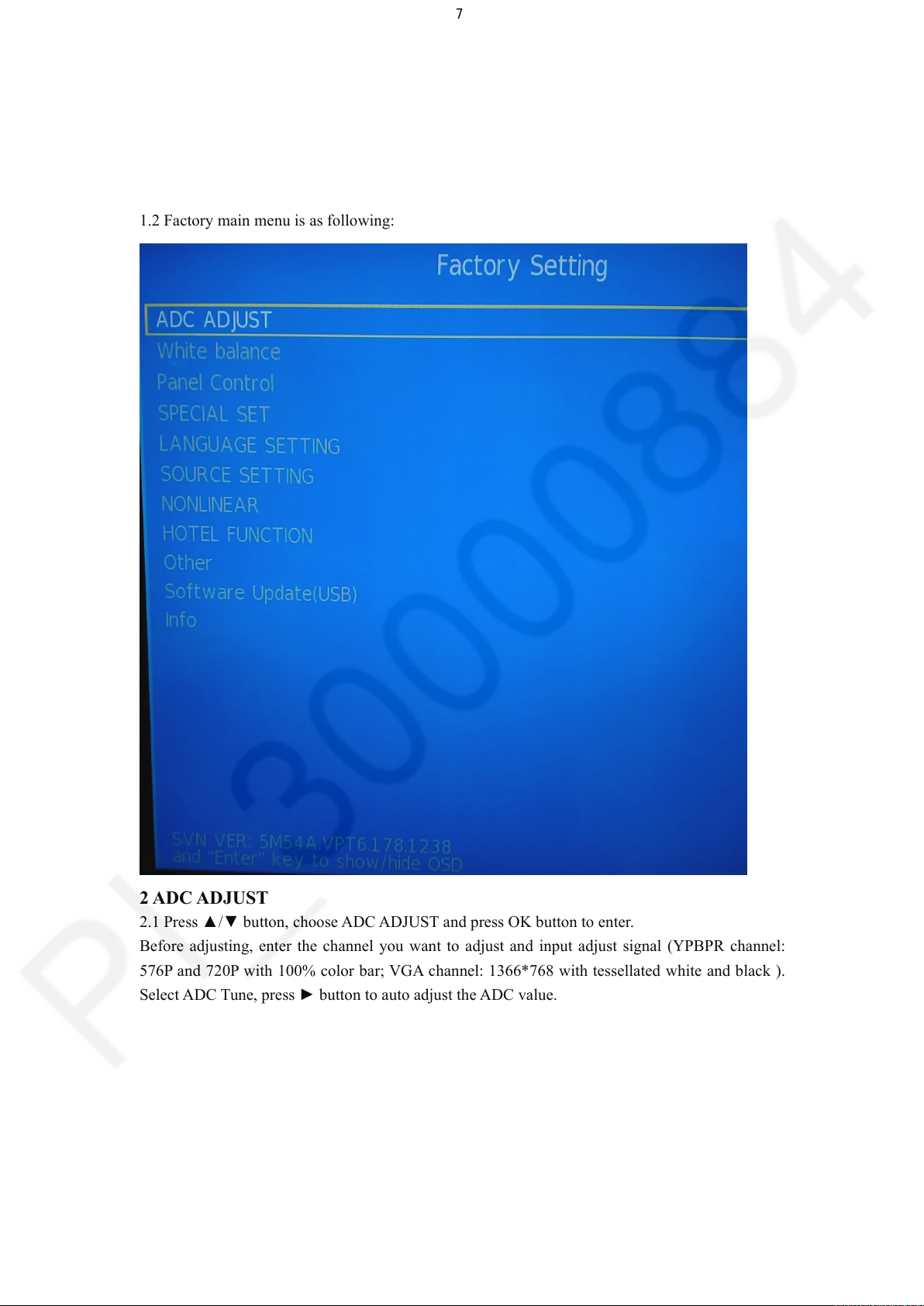
1 TO ENTER FACTORY MAIN MENU
1.1 Press AV button and follow with key 3,1,9,5 one by one.
1.2 Factory main menu is as following:
2 ADC ADJUST
2.1 Press ▲/▼ button, choose ADC ADJUST and press OK button to enter.
Before adjusting, enter the channel you want to adjust and input adjust signal (YPBPR channel:
576P and 720P with 100% color bar; VGA channel: 1366*768 with tessellated white and black ).
Select ADC Tune, press ► button to auto adjust the ADC value.
Page 8
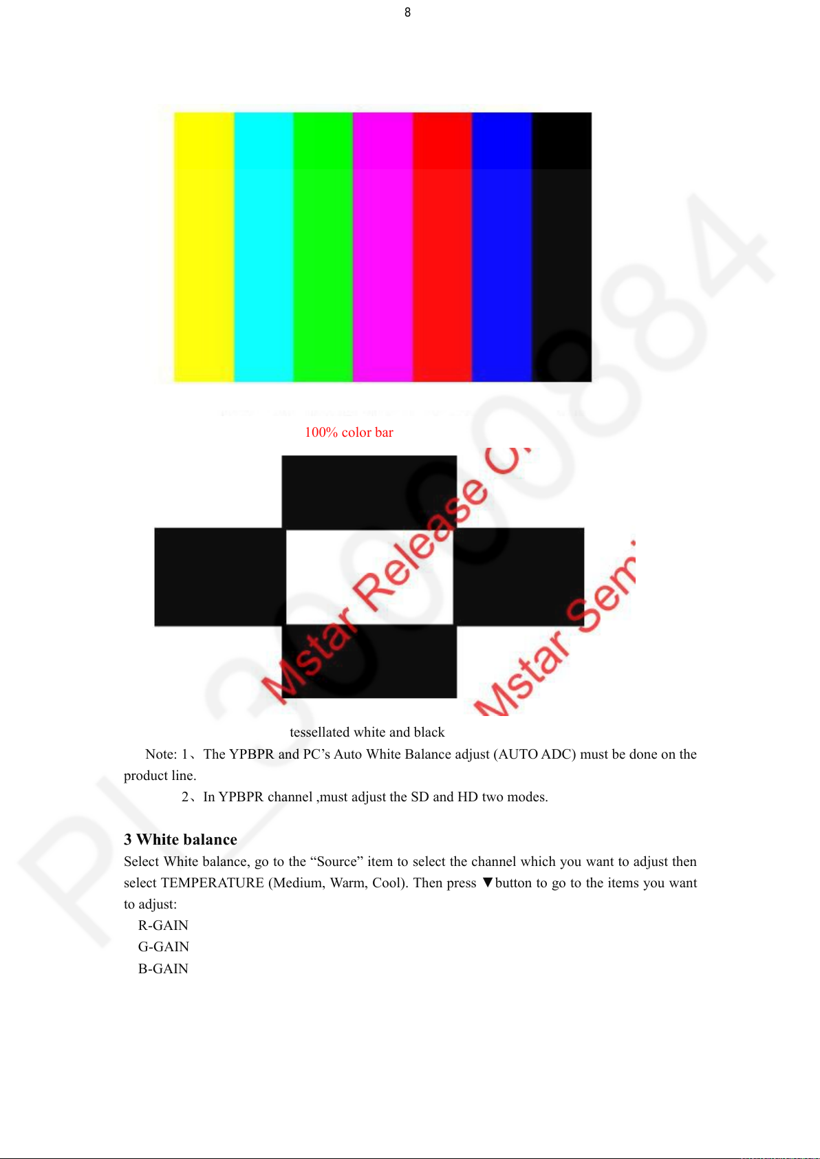
100% color bar
8
tessellated white and black
Note: 1、The YPBPR and PC’s Auto White Balance adjust (AUTO ADC) must be done on the
product line.
2、In YPBPR channel ,must adjust the SD and HD two modes.
3 White balance
Select White balance, go to the “Source” item to select the channel which you want to adjust then
select TEMPERATURE (Medium, Warm, Cool). Then press ▼button to go to the items you want
to adjust:
R-GAIN
G-GAIN
B-GAIN
R-OFFSET
G-OFFSET
B-OFFSET
Page 9
Press◄/► buttons can adjust the value to the best effect.
9
COPY ALL : Copy the values to all source!
4 Panel Control
No adjust.
5 SPECIAL SET
FAC. HOTKEY
Press◄/► button to switch factory hotkey on or off. For shipping condition, this item should be
off.
OUT FAC SOUND SYS
No adjust.
WHITE PATTERN
No adjust. For shipping condition, this item should be off.
2HOUR OFF
No adjust. For shipping condition, this item should be off.
BLUE SCREEN
No adjust.
Factory Reset
Choose and enter 8899 to execute factory reset.
DLC
No adjust.
WHITE BLACK STRENTH
No adjust.
power
Press◄/► button to switch AC power on status. Last is power on memorized, Force Standby is
power on standby, Force On is power on always.
OUT FACTORY SET
Press ► button to reset system to shipping condition.
AGING MODE
Press◄/► button to switch aging mode on or off. When aging mode is on, press EXIT button to
exit this mode.
CHANNEL RESET
Press ► button to load channel preset for factory test.
4 LANGUAGE SETTING
No adjust.
5 SOURCE SETTING
No adjust.
6 NONLINEAR
MODE
Choose source.
Brightness Curve
Adjust the Brightness Curve.
Contrast Curve
Adjust the Contrast Curve.
Saturation Curve
Page 10
Adjust the Saturation Curve.
10
Hue Curve
Adjust the Hue Curve.
Sharpness Curve
Adjust the Sharpness Curve.
Volume Curve
Adjust the Volume Curve.
7 HOTEL FUNCTION
No adjust.
8 Other
SSC
Press OK to set the appropriate EMC values.
UART DEBUG
Press ► button to set UART DEBUG status. HK for debug, None to turn off debug status.
VIF1
No adjust.
POWER ON LOGO
When hotel mode is on, this item will be available. Select to turn on or turn off power on logo.
Spdif Audio Delay
No adjust.
SET LOGO MSTLOGO.JPG
No adjust.
BACK DATA TO USB
No adjust.
LOAD DATA FROM USB
No adjust.
Country Code
No adjust.
OSD Language
No adjust.
INIT_ADC_WHITE
Press ► button to load default white balance data.
Stick Demo
No adjust.
INIT LANGUAGE SETTING
No adjust.
Mirror Enable
Press◄/► button to switch mirror function on or off.
Channel Info Save
Press◄/► button to save current channel table to USB.
Channel info Update
Press◄/► button to load channel table from USB.
SW&DB update
No adjust.
Page 11
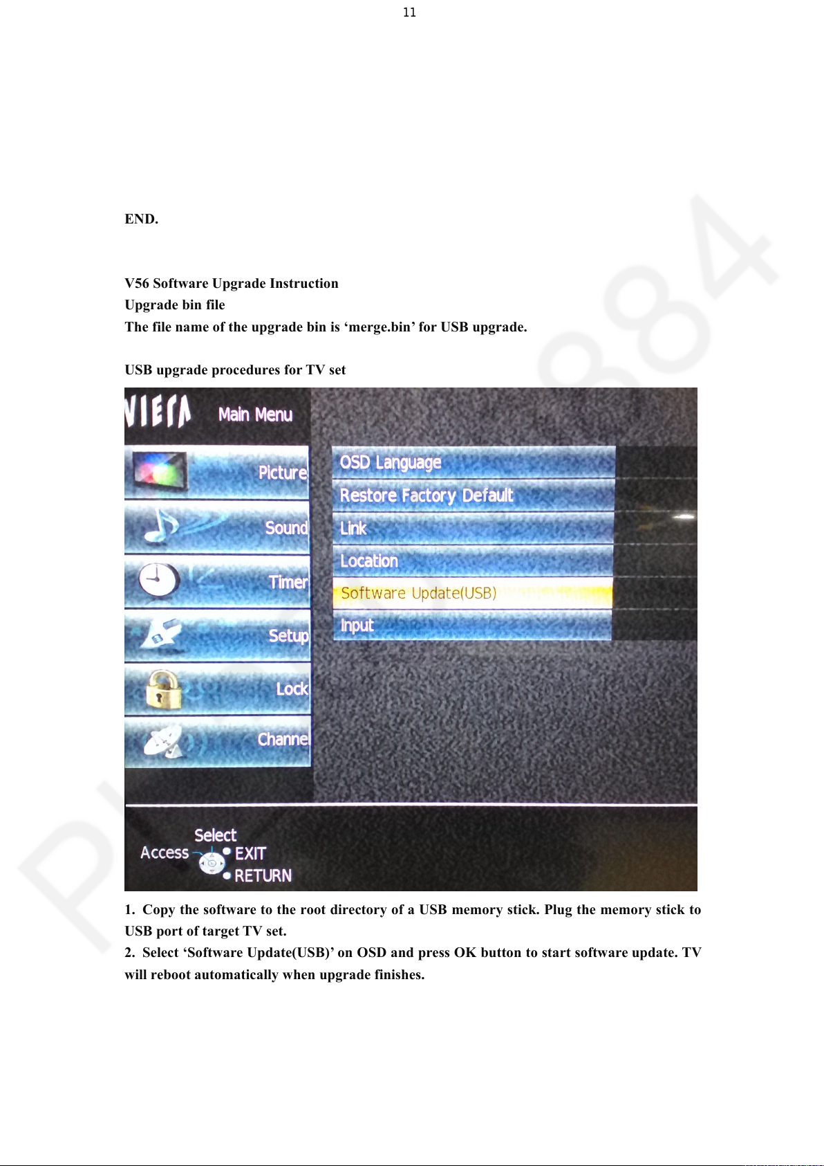
8 Software Update(USB)
1. Copy the software to the root directory of a USB memory stick. Plug the memory stick to
2. Select ‘Software Update(USB)’ on OSD and press OK button to start software update. TV
3. If the process stop at 19% and TV reboot, it means the software of both TV set and USB
11
Press OK button to update software from USB.
9 Info
Press OK button to show software information.
END.
V56 Software Upgrade Instruction
Upgrade bin file
The file name of the upgrade bin is ‘merge.bin’ for USB upgrade.
USB upgrade procedures for TV set
USB port of target TV set.
will reboot automatically when upgrade finishes.
memory stick is the same.
Page 12
ISP Software Upgrade
12
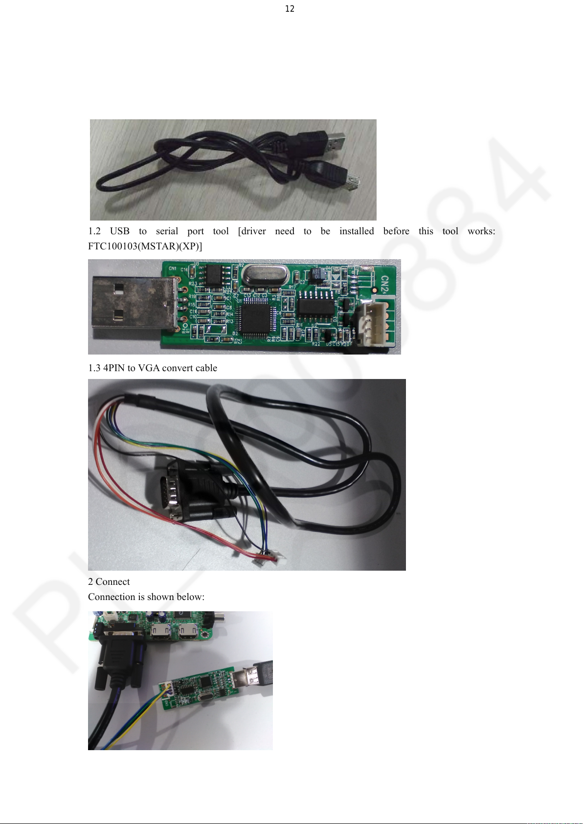
1 Hardware tools
1.1 USB cable
1.2 USB to serial port tool [driver need to be installed before this tool works:
FTC100103(MSTAR)(XP)]
1.3 4PIN to VGA convert cable
2 Connect
Connection is shown below:
Page 13
3 Driver and Upgrading applications
13
FTC100103(MSTAR) and MSTAR ISP Utility tool.
3.1 Installing driver.
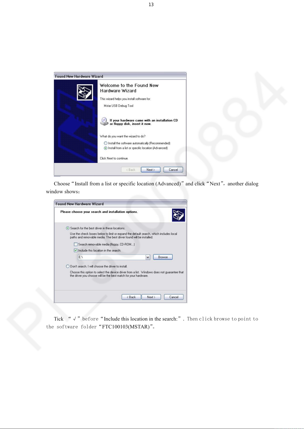
A dialog window will pop up when the upgrade tool is connected to computer through usb cable.
Choose“Install from a list or specific location (Advanced)”and click“Next”,another dialog
window shows:
Tick “√”before“Include this location in the search:”. Then click browse to point to
the software folder“FTC100103(MSTAR)”。
Page 14
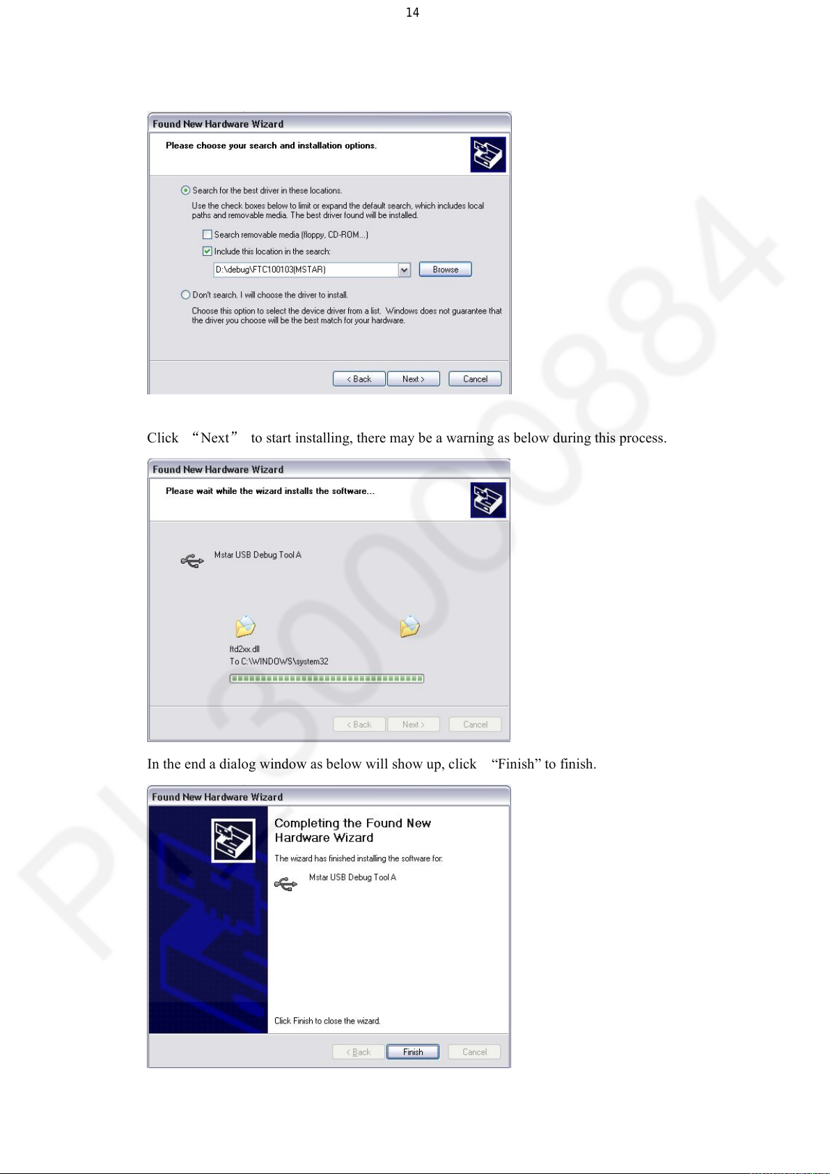
Click “Next” to start installing, there may be a warning as below during this process.
14
In the end a dialog window as below will show up, click “Finish” to finish.
Page 15
Note: there is three drive to install, so these steps should be repeated for three times. Just
15
follow the messages of the computer, the upgrade tool will not work until the three drives are
installed.
3.2 Run ISP tool to upgrade software
3.2.1 Run a Mstar ISP tool such as ‘ISP_Tool_473.exe’.
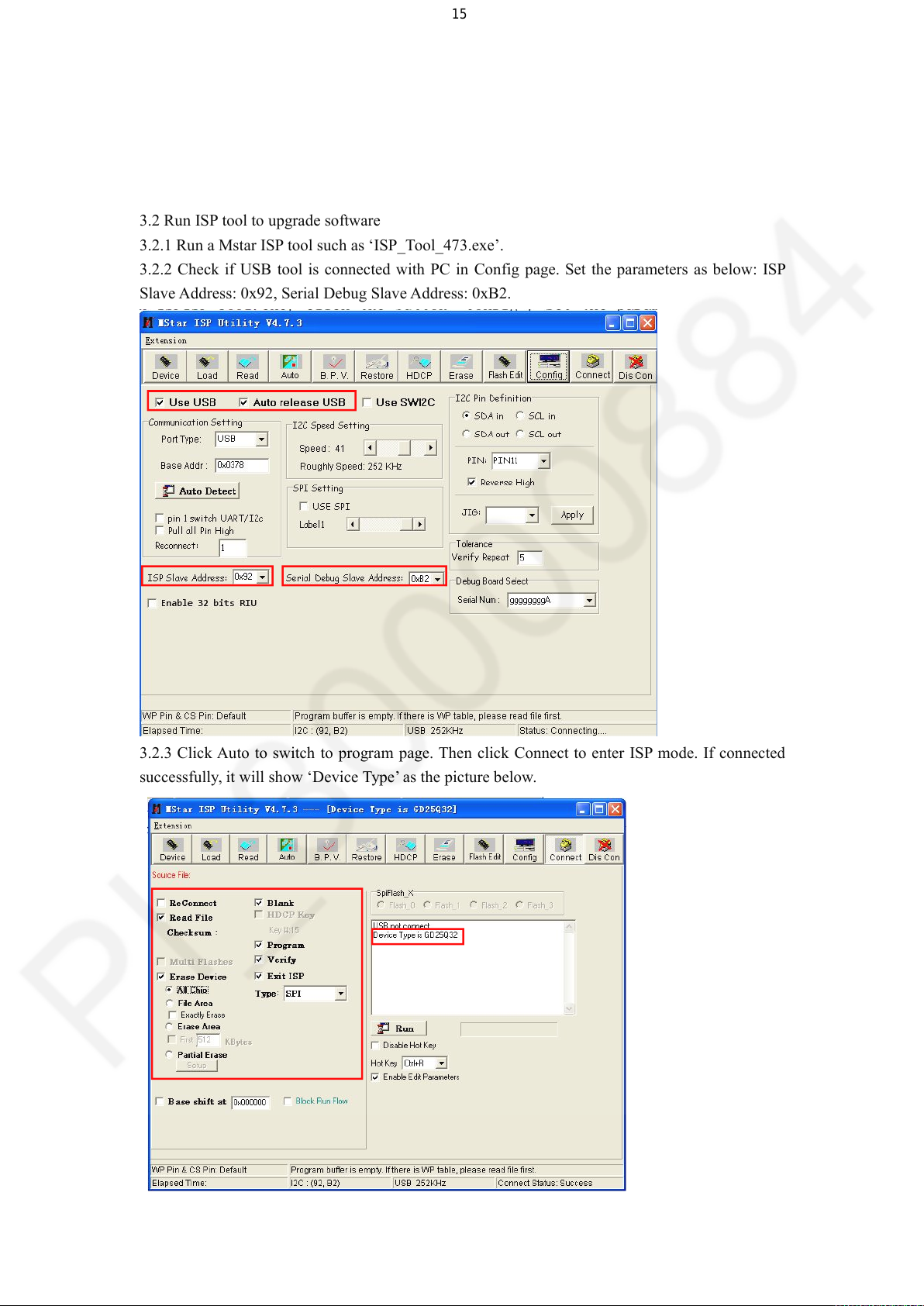
3.2.2 Check if USB tool is connected with PC in Config page. Set the parameters as below: ISP
Slave Address: 0x92, Serial Debug Slave Address: 0xB2.
3.2.3 Click Auto to switch to program page. Then click Connect to enter ISP mode. If connected
successfully, it will show ‘Device Type’ as the picture below.
Page 16
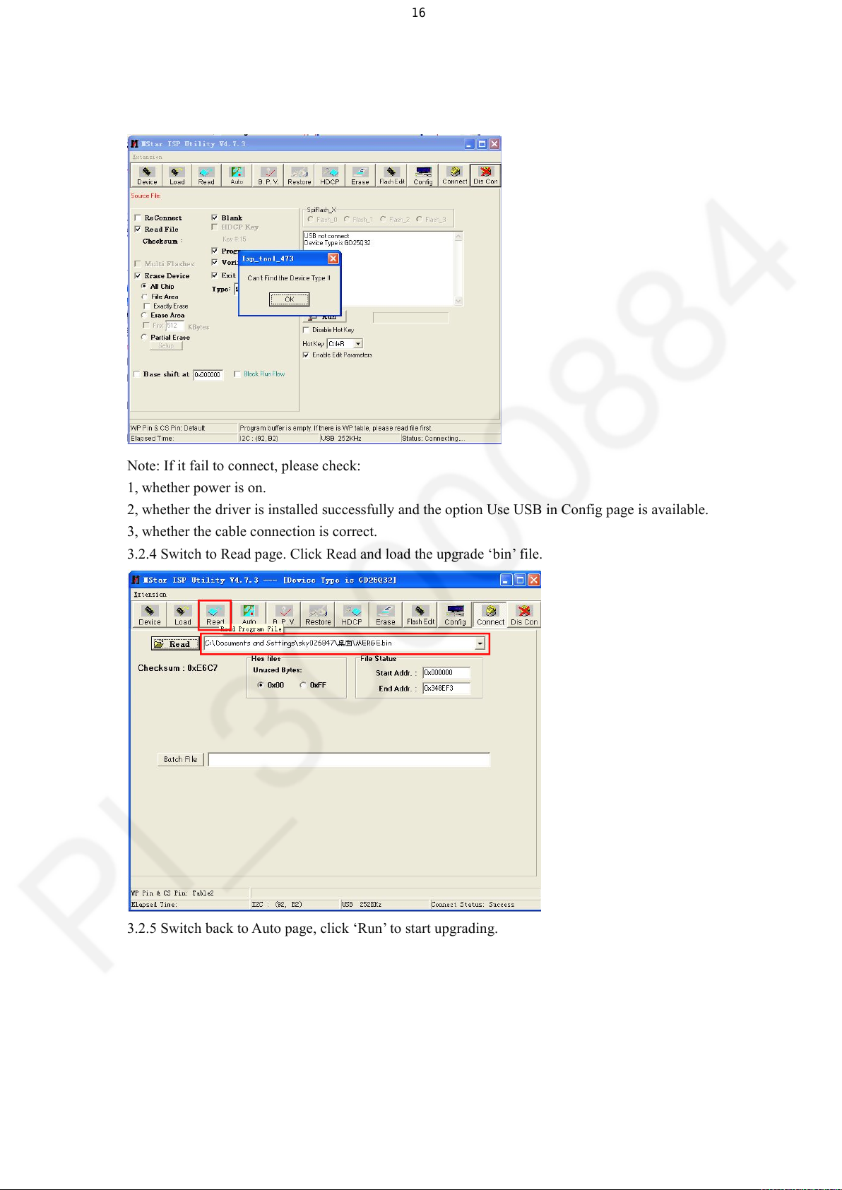
If connect failed, it will show ‘Can’t Find the Device Type !!’.
16
Note: If it fail to connect, please check:
1, whether power is on.
2, whether the driver is installed successfully and the option Use USB in Config page is available.
3, whether the cable connection is correct.
3.2.4 Switch to Read page. Click Read and load the upgrade ‘bin’ file.
3.2.5 Switch back to Auto page, click ‘Run’ to start upgrading.
Page 17
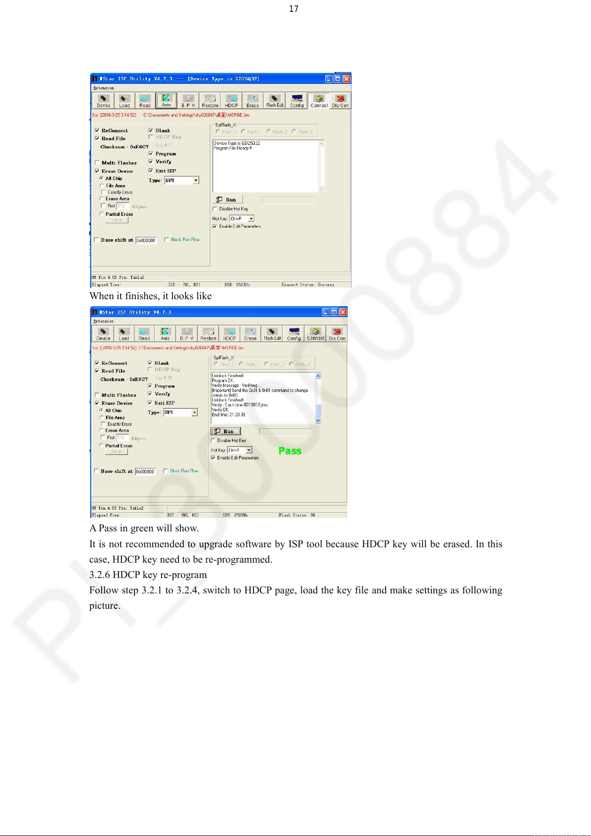
When it finishes, it looks like
17
A Pass in green will show.
It is not recommended to upgrade software by ISP tool because HDCP key will be erased. In this
case, HDCP key need to be re-programmed.
3.2.6 HDCP key re-program
Follow step 3.2.1 to 3.2.4, switch to HDCP page, load the key file and make settings as following
picture.
Page 18

Switch back to Auto page, make settings as following picture. Partial Erase address must be set to
18
0x003B0000.
Page 19

When it finishes, it looks like
19
A Pass in green will show.
Hotel Mode
Enter Hotel Mode: MENU+7906.
Enter Hotel Mode state:
Page 20

Hotel Mode
20
Press◄/► button to turn on or turn off hotel mode.
Initial INPUT
Press◄/► button to switch power on source.
Initial POS
Only available when Initial INPUT switch to ATV. Press◄/► button to set power on TV channel.
Initial VOL Level
Press◄/► button to set power on volume.
Maximum VOL Level
Press◄/► button to set maximum volume user can adjust.
Button Lock
Press◄/► button to lock or unlock panel buttons.
Remote Lock
Press◄/► button to lock or unlock remote control. When on, only hotel mode is available
(MENU+7906).
Auto Power On
Press◄/► button to set power on status. Last is power on memorized, Off is power on standby,
On is power on always.
Input Select Mode
Press OK to enter Input Select Mode. User can turn on or turn off input source in input menu.
Data Copy To USB
Press OK to copy current TV data to USB.
Data Copy From USB
Press OK to copy TV data from USB which has been previously copied.
Page 21

Block Diagram
AC INPUT
POWER
CONTROL
UNIT
U0A3
AMP
VCC=12V
D1D1=12V
VLED≈50V
U0P7
12V to 5V
U0P3/U0P6
5V to 3.3V
U0P5
5V to 1.8V
U0P4
5V to 1.15V
21
System Block Diagram
Key check point
Page 22

Circuit Block Diagram
+3.3V_Standby
+3.3V_TUNER
+12V
IR Control
AS1117L
AS1117L
AS1117L
Key Control
SPI FLASH
AOZ3015
I2C
DC TO DC
DC TO DC
I2S
DC TO DC
DC TO DC
+12V_PANEL
ME9435A
USB2.0
TSUMV56
SPR
SPL
TUNER
IF
TAS5707
R
L
V
32Mbit
LVDS SIGNAL
+1.8V_DDR2
+5V_Norm al
EARPHONE
HDMI2
+5V_Standby
AV
SPDIF
(COAXIAL)
INTERNAL POWER SUPPLY
RF
HDMI1
G5728
+5V_Stb
DC TO DC
VDDC_1.15V
PC
HD PANEL
Power Tree
Schematics
22
Page 23

5
23
4
3
2
1
Page-02 Function Block
D D
+5V_Standby
+5V_Normal
C C
+5V_Standby
+5V_Normal
INTERNAL POWER SUPPLY
+12V
ME9435A
DC TO DC
AS1117L
DC TO DC
AS1117L
DC TO DC
G5728TO1U
DC TO DC
AS1117L
DC TO DC
+12V_PANEL
+5V_Standby
+3.3V_Standby
+1.8V_DDR2
VDDC_1.15V
+3.3V_TUNER
IR Control
SPI FLASH
32Mbit
FHD PANEL
LVDS SIGNAL
MSD3553/V56
USB2.0
HDMI1(MHL3.0)
Key Control
B B
IF
IF
SPR
R
L
TUNER
EARPHONE
V
L
AV
R
TPA3144
SPL
A A
5
SPDIF
(OPTICAL)
4
HDMI2
PC
DEBUG
3
RF
Title
Title
Title
Size Document Number Rev
Size Document Number Rev
Size Document Number Rev
Date: Sheet of
Date: Sheet of
2
Date: Sheet of
MSD3553(5M53N-49E2000)
<Title>
<Title>
Custom
Custom
Custom
<Title>
<Doc>
<Doc>
<Doc>
Function block
00_B 10Friday, November 27, 2015
00_B 10Friday, November 27, 2015
00_B 10Friday, November 27, 2015
1
00.00
Page 24

5
24
4
3
2
1
D D
12V/1920mA
5V/2330mA
AOZ3015
12V
C C
POWER IN
5V/230mA
5V/350mA
5V_Normal/3350mA(1750MA)
ME2345A
STB_EN
5V_Normal
5V_Normal
G5728
LD1117-3.3
LD1117
AMS1117-3.3V 3.3V_TU/200MA5V_Normal
FUSE
1.15V/1000mA
3.3V_stb/350mA
1.8V_DDR/150mA?
5V_USB/1000mA(500MA)
MSD3553
5Amax
Istb=16mA
B B
12V/3A
12V/1.5A
G524C3
ME9435
TPA3140D2
5V_MHL/2000mA(900MA)5V_Normal
VCC_Pannel /1.5AIN
A A
Title
Title
Title
Size Document Number Rev
Size Document Number Rev
Size Document Number Rev
A
A
A
Date: Sheet of
Date: Sheet of
5
4
3
Date: Sheet of
MSD3553(5M53N-49E2000)
<Title>
<Title>
<Title>
<Doc>
<Doc>
<Doc>
2
Power tree
00_C 10Friday, November 27, 2015
00_C 10Friday, November 27, 2015
00_C 10Friday, November 27, 2015
1
Page 25

5
25
4
3
2
1
PIN NAME
35 AUL4
36 AUR4
39
LINEOUTL3
40
D D
C C
B B
LINEOUTR3
51
GPIO44/TX1
GPIO45/RX1
52
82
GPIO3
84
GPIO1
85
GPIO0/SPDIF_OUT
PWM0
86
87 PWM1/MHL_VBUS
88 IRIN
31
101
102
38 AUR5
37 AUL5
AUR0
SAR0
SAR1
FUNCTION
AV/VGA AUDIO IN -L
AV/VGA AUDIO IN -R
Amplifier Input _L
Amplifier Input _L
SDA
SCL
PANEL_ON/OFF
PWR_ON/OFF
SPDIF_OUT
BRI_ADJ
AMP_MUTE
IR-in
EAR_DETECT
KEY0-in
KEY1-in/VBL_CTR L KEY1-in/VBL_CTR L
EAR-MUTE
AMP_RST_1
公版 备注
AV/YUV AUDIO IN -L
AV/YUV AUDIO IN -R
AVOUT_L
AVOUT_R
SDA
SCL
PANEL_ON/OFF
PWR_ON/OFF
SPDIF_OUT
BRI_ADJ
AMP_MUTE
IR-in
EAR_DETECT
KEY0-in
A A
MSD3553(5M53N-49E2000)
Title
Title
Title
<Title>
<Title>
<Title>
Size Document Number Rev
Size Document Number Rev
Size Document Number Rev
<Doc> 00.00
C
<Doc> 00.00
C
<Doc> 00.00
C
Date: Sheet of
Date: Sheet of
5
4
3
2
Date: Sheet of
GPIO
00_D 10Friday, November 27, 2015
00_D 10Friday, November 27, 2015
00_D 10Friday, November 27, 2015
1
Page 26
5
26
4
3
2
1
2015-10-15: 修改KEY1_OUT网络从CN0S2的8PIN到9PIN
2015-10-15: 删除I2S网络无用的测试点
2015-10-15: H1螺钉孔改为4.0
2015-10-15: 修改AMP_MUTE网络
D D
2015-10-15: 修改串口网络
2015-10-21: 增加测试点
2015-10-22: 增加主芯片散热片
2015-10-22: 更改C3M7、C4M9、R0A13封装
2015-11-07: 修改AV左右声道输入问题
2015-11-12: 更改耳机静音电路,解决交流关机冲击声
2015-11--27: 取消耳机运放,修改耳机静音电路
C C
B B
A A
Title
Title
Title
Size Document Number Rev
Size Document Number Rev
Size Document Number Rev
Date: Sheet of
Date: Sheet of
5
4
3
Date: Sheet of
MSD3553(5M53N-49E2000)
<Title>
<Title>
<Title>
<Doc>
A
<Doc>
A
<Doc>
A
2
00.00
00_A 10Monday, November 30, 2015
00_A 10Monday, November 30, 2015
00_A 10Monday, November 30, 2015
1
Page 27

5V Power(option) 3A
27
5
EN
R3P4
C3P5
47KΩ
100nF
R3P6
100KΩ
+12V_PWR
+12V_NOR
D D
C6P7
10uF C8P3
U0P7
1
8
EN
7
LX
6
COMP
5
AOZ3015AI
FB4IN
5
EN
6
BST
U0P1
L0P5
SW
10uH
FB7
R5P6
20KΩ
C7P5
NC/1nF
1nF
FB7
EN
FB7SW
C0P2 NC/1uF
R0P2 NC/0Ω
Vout=0.8x(1+(R1/R2))
10V
R1=R5P9+R6P7 R2=R6P9
C7P8
C7P7
R5P9
C7P6
1.8KΩ
100nF
10uF
NC/100nF
R6P7
R6P6
51KΩ
NC/1.8KΩ
R6P9 10KΩ
PGND
2
VIN
3
AGND
VCC4FB
C6P9
C6P8
100nF
100nF
3
2
SW
SW
1
GND
NC/MP1470GJ-Z
4
5V SWITCH
+5V_STB
C7P9
CE0P9
+
10uF
220uF
16V
STANDBY
L :Power off
H :Power on
+5V_STB
Q0P3
R2P3
C3P8
100KΩ
1uF
±5%
16V
R2P4
4.7KΩ
±5%
R2P5
4.7KΩ
KMBT3904
1
±5%
Q0P1
2 3
3
+5V_NOR
23
AO3401A
1
CE0P1
C3P9
+
NC/100uF
100nF
16V
2
1
VDDC_1.15V
U0P4
4
C C
C0P5
C1P7
10uF
16V
100nF
16V
Vout=0.6x(1+(R1/R2))=1.164 V
R1=R2P2+R1P2
LX3VIN
L0P3
2
3.3uH
GND
R1P10
1
5
FB8
10KΩ
EN
FB
G5728TO1U
FB8
R1P9
R1P1
100KΩ
NC/100KΩ
R2=R1P10
+1.8V_DDR2
4
U0P5
OUT
B B
R1
R2
DDR2:R1P11=1K R0P5=470R
DDR3:R1P11=1K R0P5=220R
AS1117L/TR-HF
IN3OUT2ADJ
R1P11
1KΩ
1
+1.8V/1.5V_DDR
C1P14
C1P15
C1P16
C1P13
10uF
10uF
16V
100nF
100nF
R0P5
6.3V
16V
16V
470Ω
+5V_NOR
Vout=1.25V*(R1+R2)/R1
C1P6
33pF
R2P2
C1P12
50V
1.2KΩ
10uF
16V
R1P2
8.2KΩ
+3.3V_TUNER
AS1117L-3.3/TR-HF
+5V_NOR
10uF
+1.15V_VDDC+5V_STB
C1P11
100nF
CE0P2
C1P10
+
16V
100uF
NC/10uF
6.3V
4
U0P3
OUT
IN3OUT2ADJ
1
C1P3
+3.3V_AUDIO
C1P5
C1P2
C1P1
100nF
10uF
100nF
16V
16V
16V
16V
FB0P1
60Ω/100MHz
+3.3V_TUNER
+3.3V_Normal
AS1117L-3.3/TR-HF
+5V_STB
screw hole & MARK
H1
4
5
6
123
7
8
9
Screw Hole
H3
4
5
6
123
7
8
9
Screw Hole
H5
4
5
6
123
7
8
9
Screw Hole
4
U0P6
OUT
IN3OUT2ADJ
1
+3.3V_Standby
C3P0
C3P1
C2P9
C3P2
+3.3V_Normal
100nF
10uF
10uF
100nF
16V
16V
16V
16V
H2
MARK1
MARK2
4
5
6
123
7
8
9
Screw Hole
H4
4
5
6
123
7
8
9
Screw Hole
MARK3
MARK
MARK
MARK
MARK4
MARK
Power for panel
ME9435A
C0P12
C0P4
100nF
16V
R1P8
6.8KΩ
5
220nF
50V
R0P4
10KΩ
±5%
C0P3
NC/10uF
R0P9
100KΩ±5%
16V
CE1P0
NC/1N4148W
1
Q0P2
KMBT3904
2 3
R0P1,R0P4根据实际情 况选取阻值
±5%
C0P11
PANEL_ON/OFF
PANEL_ON/OFF
+12V_NOR
L :Power off
H :Power on
+3.3V_Normal
R0P1
NC/10KΩ
R0P3
±5%
10KΩ
±5%
A A
VCC_PANEL
3
S
2
1
8
G
4
7
6
C0P1
CE0P3
5
100nF
+
D
100uF
U0L1
100nF
16V
Note:靠近 VB1
16V
16V
端子
MSD3553(5M53N-49E2000)
Title
Title
Title
<Title>
<Title>
<Title>
POWER
Size Document Number Rev
Size Document Number Rev
Size Document Number Rev
<Doc>
D
<Doc>
D
<Doc>
D
Date: Sheet of
Date: Sheet of
4
3
2
Date: Sheet of
1
1 10Monday, November 30, 2015
1 10Monday, November 30, 2015
1 10Monday, November 30, 2015
00.00
Page 28
5
28
4
3
2
1
+12V_PWR
D1D3
1N4148W
+42V
R5D5
120KΩ
Q0D8
1
3
1
3
Z0D7
15V
D1D9
HBR20150S
D1D1
HBR2045
2 3
HS0D1
HEAT SINK
HS
213
2
+
+
C3D5
C3D4
C3D1
470uF
HS0D2
HEAT SINK
HS
213
2
+42V
R5D2
4.7KΩ
Z0D8
47V
D1D4
1N4148W
R8D1
1KΩ
C2D3
100nF
R9D1
47KΩ
C1D02
100nF
R5D6
R6D1
47KΩ
100KΩ
1
C4D6
100nF
C3D6
1000uF
C3D2
100nF
100nF
470uF
C3D7
1000uF
C3D9
R5D1
100nF
2KΩ
+
+
OVP
R4D4
100Ω
1
KMBT3904
Q0D5
2 3
R8D5
10KΩ
STB
1
STANDBY
GND
+42V
+42V
1
1
1
2
R4D9
39KΩ
CN1D3
+12V
+12V_PWR
1
C4D0
1
2
100nF
CN1D2
SPECIFICATION
4 4
D8D2
D8D1
1N5408
1N5408
D8D4
D8D3
1N5408
1N5408
R1D01
R1D02
1MΩ
1MΩ
CY0D1
CY0D2
470pF
470pF
3 3
CX0D2
220nF
LF0D2
4
CY0D3
47pF
L
1
N1 N2
3 2
18mHx2
TH1D3
470nF
CX0D1
R1D05
3.3MΩ
LF0D11.9mH
3 2
4
TNR0D1
680V
CN1D1
POWER SOCKET
1
Q
5Ω
R1D06
3.3MΩ
N1 N2
1
CY0D4
47pF
1-2
+
1
2 2
1
F0D1
3.15A/250V
1
R1D09
510KΩ
R1D08
1MΩ
R1D04
1MΩ
C1D5
SUPHV
2.2uF
1
C5D3
2.2uF
R1D37
1MΩ
Q
R1D16
TH1D2
1MΩ
5Ω
R1D17
820KΩ
R1D18
18KΩ
1
1
N
VD
VD
1
C0D1
1uF
R1D23
5.1KΩ
R1D10
R1D24
1.8KΩ
510KΩ
R1D20
68KΩ
R1D19
C1D4
33KΩ
470nF
C1D3
220nF
C3D0
10nF
470KΩ
R1D22
C2D9
2.2uF
D0D1
S3MB
43
N1 N2
2 6
R1D25
C1D7
12KΩ
47nF
SNSOUT
C0D2
R1D26
330pF
2.2KΩ
C4D7
NC
C1D6
NC
1
24
C3D3
*
C2D7
100nF
R1D27
5.6KΩ
C2D6
4.7nF
D0D2
S3MB
HS0D3
HEAT SINK
HS
D0D3
213
MUR460
L0D1
250uH
C2D0
100nF
2
3
COMPPFC
SNSMAINS
JCS12N65T
R1D33
D0D5
10KΩ
1N4148W
R1D32 68Ω
R1D31
22Ω
R1D29
33KΩ
D0D4
Z0D3
US1J
27V
+
C4D8
C0D3
100uF
100nF
4
5
6
7
8
9
10
11
12
NC11
PGND
SUPIC
SUPHV
GATELS
SNSOUT
SUPREG
GATEPFC
SNSAUXPFC
SNSCURPFC
TEA1716T
GATEHS13SUPHS14HB15NC1616SNSCURHBC17SGND18CFMIN19SNSBURST20SNSFB21SSHBC/EN22RCPROT23SNSBOOST
U0D2
R3D4
1KΩ
C2D5
330pF
C1D2
33nF
R0D5
10Ω
R1D28
20KΩ
SUPHV SUPHV
Q0D1
23
R1D12
1
1.5MΩ
R1D13
Z0D1
1.5MΩ
22V
R1D14
1.5MΩ
R1D35
100mΩ
C0D5
100nF
R2D5
10Ω
D0D6
US1J
C2D4
470nF
VH
VH
OVP450V
+
Z0D4
27V
Z0D5
27V
Z2D7
1KΩ
D0D7
1N4148W
R2D4
22Ω
0.5A/32V
R3D1
10Ω
R9D3
0Ω
R3D6
10Ω
F0D2
2A/250V
1
C4D3
C4D4
+
56uF
56uF
D0D8
1N4148W
R3D2
22V
22Ω
Z0D9
VCC
R1D9
10Ω
1
C6D0
+
470uF
Z0D6
22V
C2D2
100nF
R2D3
F0D5
6.8KΩ
L0D7
SUPHV
100uH
23
Q0D2
1
AOD9N50
R3D3
10KΩ
23
Q0D3
1
AOD9N50
4
STANDBY
U0D1
BPC-817C
CY0D5
1nF
STANDBY
C1D1
680pF
1
23
10KΩ
R2D6
T0D1
53
1
3
5
6 7
TRANSFORMER
D2D2
US1J
D2D1
US1J
R5D3
4.7KΩ
R5D4
2KΩ
R5D8
10KΩ
1
R5D7
27KΩ
C0D4
220nF
R6D0
4.7KΩ
+12V_PWR
12
11
10
9
8
R6D2
100KΩ
C5D9
100nF
R5D9
16.3KΩ
KMBT3904
72
D1D7
US1J
D1D6
US1J
C1D0
22nF
OVP
2
U0D3
3
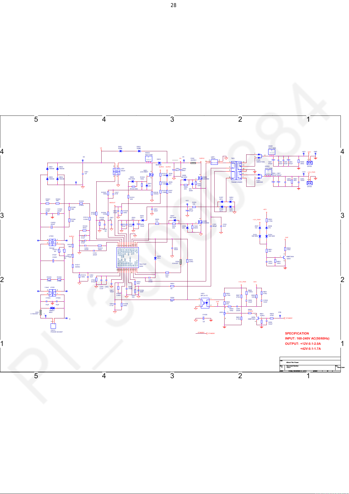
INPUT: 160-240V AC(50/60Hz)
1 1
OUTPUT: +12V:0.1-2.0A
+42V:0.1-1.7A
Title
Title
Title
65inch Thin Power
65inch Thin Power
65inch Thin Power
Size Document Number Rev
Size Document Number Rev
Size Document Number Rev
<Doc> <RevCode>
C
<Doc> <RevCode>
C
<Doc> <RevCode>
C
Date: Sheet of
Date: Sheet of
Date: Sheet of
5
4
3
2
1 2Friday, November 27, 2015
1 2Friday, November 27, 2015
1 2Friday, November 27, 2015
1
Page 29

5
29
4
3
2
1
TAS5 707
FB0A4
60Ω/100MHz
22.1KΩ
R5A8
R6A0
C9A1
100nF
R6A6 18.2KΩ
C1A07
22pF
R5A9
470Ω
470Ω
C7A7 NC/2.2nF
C7A9
C7A8
4.7nF
C8A2
C8A1
4.7nF
C8A0 1uF
47nF
47nF
33nF
C8A3
1
3
4
5
6
7
8
9
10
11
12
NC8
R6A2
AVSS
BST_A
AVDD
/FAULT
MCLK
OSC_RES
DVSS
VR_DIG
/PDN
LRCLK
SCLK
SDIN
SDA
SCL
C1A14
100nF
OC_ADJ
VR_ANA
SSTIMER
PLL_FLTP
PLL_FLTM
GVDD_OUT
U0A3
TAS5707PHPR
/RESET25/STEST26DVDD27DVSS28GND29AGND30VREG31GVDD_OUT32BST_D33PVDD_D34PVDD_D35OUT_D
C1A11
C1A12
100nF
1uF
C1A15 33nF
OUT_A
PVDD_A2PVDD_A
GND
PGND_AB
PGND_AB
OUT_B
PVDD_B
PVDD_B
BST_B
BST_C
PVDD_C
PVDD_C
OUT_C
PGND_CD
PGND_CD
36
10KΩ
R6A3
13
NC/0Ω
14
15
16
17
18
19
C9A9
20
100nF
21
22
23
24
AMP_RST#
+3.3V_AMP
C1A4
10uF
VDD_AMP
CE0A7
C8A6
C8A5
+
220uF
100nF
1nF
49
48
47
46
45
44
43
C9A2 33nF
42
VDD_AMP
41
40
39
C1A01
C1A00
C1A02
38
37
1nF
33nF
100nF
C1A09
CE0A5
C1A08
+
100nF
220uF
1nF
R6A1
C8A8
330pF
VDD_AMP
C9A3
C9A4
1nF
100nF
R7A2
22Ω
VDD_AMP
C1A04
330pF
R7A4
22Ω
C1A17
330pF
L0A7 22uH
22Ω
R6A5
22Ω
C9A7
330pF
L0A9 22uH
L1A0 22uH
L+
L
C8A4
470nF
C8A9
NC/470nF
CN0A1
L-
1
2
L0A8
22uH
C9A5
470nF
C1A03
470nF
C1A16
470nF
3
4
CN_M
R+
R
C1A05
NC/470nF
R-
D D
C C
60Ω/100MHz
FB0A3
+3.3V_AUDIO +3.3V_AMP
F0A3
5A/32V
+12V_NOR VDD_AMP
+3.3V_AMP
I2S_MCK_OUT
R6A4
220Ω
R6A7 NC/10KΩ
+3.3V_Normal
I2S_LRCK_OUT
R6A8 220Ω
I2S_BCK_OUT
R6A9 220Ω
I2S_DATA_OUT
R7A0 220Ω
M_SDA
R7A1 100Ω
M_SCL
R7A3 100Ω
Close to SOC IC
C1A6
10uF
C9A6
22pF
C9A8
4.7uF
AMP_PDN#
C1A06
22pF
EARPHONE/LINE OUT
EAR_DETECT
+3.3V_AUDIO
JA0A1
R2A2
R0A10
1
NC/10KΩ
0Ω
2
EAR-DETECT
±5%
±5%
3
AMP-PRout
4
AMP-PLout
EAR_R
EPHONE SOCKET
EAR_L
手插
MUTE CONTROL
L :Normal
H :Mute
R1A2
NC/0Ω
+5V_STB
R1A3
+12V_PWR
0Ω
D0A2
R1A1 10KΩ
1N4148W
±5%
R1A7
NC/100KΩ
CE0A1
+
±5%
100uF
B B
16V
解决交流关机冲击声
L :Normal
H :Mute
AMP-MUTE
AMP_RST
H: ACTIVE
A A
L: RESET
AMP-MUTE AMP_PDN#
R7A6
1KΩ
R0A13
NC/10KΩ
H :Normal
L :Mute
R4A12
NC/33KΩ
AMP_RST#AMP_RST
D0A4
+3.3V_Standby
BAV70
2
3
1
3
1
Q0A2
C
B
E
MMBT3906
2
R0A1
NC/4.7KΩ
EAR-MUTE
2
±5%
+3.3V_Standby
R1A9
47KΩ
H: UNMUTE
L: MUTE
R1A4
10KΩ
R1A6
10KΩ
1
±5%
±5%
HP/MUTE
±5%
KMBT3904
Q0A3
2 3
CE3A2 220uF16V
CE3A1 220uF16V
R8A8 0Ω
+
R8A7 0Ω
+
R8A6
1KΩ
AV-AUOUTR0
AV-AUOUTL0
1
Q0A6 2N7002K
2 3
R8A5
1KΩ
2 3
C1A1
10uF
1
AMP-PRout
AMP-PLout
Q0A7
2N7002K
I2S_MCK_OUT
I2S_LRCK_OUT
I2S_BCK_OUT
I2S_DATA_OUT
M_SDA
M_SCL
I2S_MCK_OUT
I2S_LRCK_OUT
I2S_BCK_OUT
I2S_DATA_OUT
M_SDA
M_SCL
MSD3553(5M53N-49E2000)
Title
Title
Title
<Title>
<Title>
<Title>
Size Document Number Rev
Size Document Number Rev
Size Document Number Rev
Date: Sheet of
Date: Sheet of
5
4
3
2
Date: Sheet of
Amplifier
<Doc> 00.00
D
<Doc> 00.00
D
<Doc> 00.00
D
1
2 10Thursday, December 03, 2015
2 10Thursday, December 03, 2015
2 10Thursday, December 03, 2015
Page 30
5
<RevCode>
<RevCode>
<RevCode>
30
D D
+12V_PWR
C1B0
1uF
C C
BL-ON/OFF
BL_ON/OFF
BL-ADJUST
BL-ADJUST
B B
BL-ADJUST
BL_ON/OFF
R0B10
68Ω
+
C0B2
220uF
1
R0B2
C1B1
2KΩ
NC
C0B3
1uF
R0B11
68Ω
C0B0
470nF
R4B0
120KΩ
R4B1
20KΩ
R0B3
68Ω
R0B1
0Ω
1
R4B9
2KΩ
C1B2
NC
R4B8
20KΩ
BL-ADJUST
BL_ON/OFF
C3B10
100nF
BL_VIN
FB1
CTL1
FB2
CTL2
FB3
CTL3
FB4
CTL4
4
1
U0B1
1
VIN
2
VCC
3
COMP
4
OSC
5
EN/PWM
6
DIM
7
FB1
8
CTL1
9
FB2
10
CTL2
11
FB3
12
CTL3
13
FB4
CTL414CTL5
MP3373GM-Z
PSEN
GATE
ISENSE
GND
FAULT
CTL8
CTL7
CTL6
3
C0B8
R4B2
100pF
10Ω
R0B9
10KΩ
R8B0
4.7Ω
R8B3
4.7Ω
Q1B0
AOD256
1
FB1
R1B3
R1B0
10Ω
R3B0
10Ω
10Ω
1
1
2
3
D0B1
HBR20150S
C0B5
100pF
23
R4B3
10Ω
R4B5
R4B4
270mΩ
270mΩ
R2B0
5.1KΩ
1
R5B0
*
R2B3
5.1KΩ
1
R3B3
10Ω
R5B6
*
C0B6
+
82uF
R4B6
270mΩ
270mΩ
R8B4
LED1
CTL6 CTL5
23
4.7Ω
Q0B0
2SA1013-O
R5B1
*
R8B2
LED4
CTL3CTL4 CTL2
23
4.7Ω
Q0B3
2SA1013-O
R5B7
*
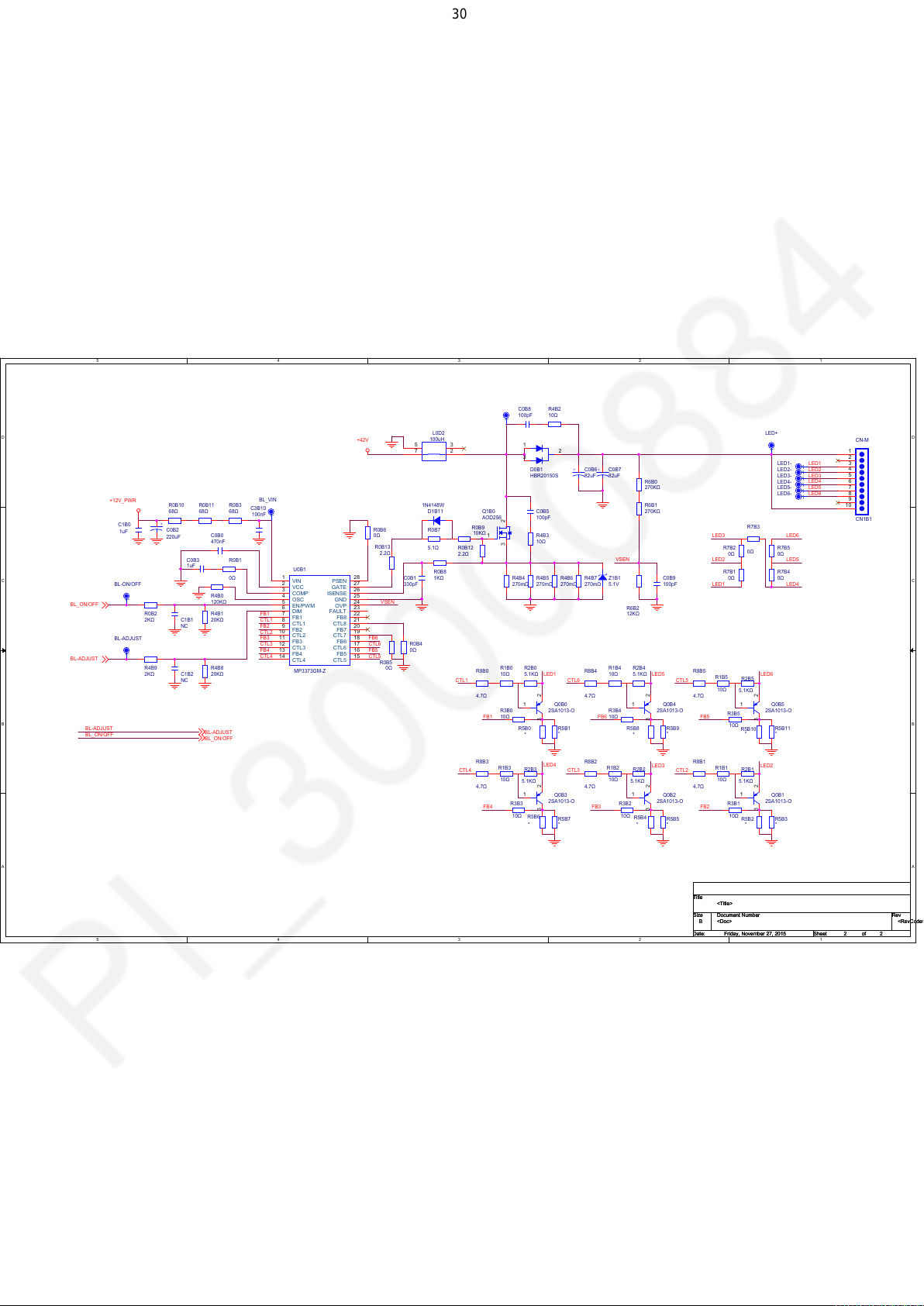
L0D2
+42V
R0B6
0Ω
R0B13
2.2Ω
28
27
26
25
24
VSEN
OVP
23
22
FB8
21
20
FB7
19
18
FB6
FB6
17
CTL6
16
FB5
FB5
15
CTL5
R0B5
100uH
5 3
7 2
1N4148W
D1B11
R0B7
R0B12
5.1Ω
2.2Ω
R0B8
1KΩ
C0B1
330pF
R0B4
0Ω
0Ω
CTL1
2
LED+
C0B7
+
82uF
R6B0
270KΩ
R6B1
270KΩ
R7B3
R7B2
0Ω
R8B5
4.7Ω
R8B1
4.7Ω
0Ω
LED2
R7B1
0ΩR4B7
LED1
LED6
R1B5
R2B5
10Ω
5.1KΩ
23
1
Q0B5
2SA1013-O
R3B5
FB5
10Ω
R5B10
*
R1B1
R2B1
10Ω
5.1KΩ
23
1
Q0B1
2SA1013-O
R3B1
FB2FB3FB4
10Ω
R5B2
*
VSEN
Z1B1
5.1V
R1B4
10Ω
R3B4
FB6
10Ω
R1B2
10Ω
C0B9
100pF
R6B2
12KΩ
R2B4
LED5
5.1KΩ
23
1
Q0B4
2SA1013-O
R5B8
R5B9
*
*
LED3 LED2
R2B2
5.1KΩ
23
1
Q0B2
2SA1013-O
R3B2
10Ω
R5B4
R5B5
*
*
1
LED1-
LED2-
LED3-
LED4-
LED5-
LED6-
R7B5
0Ω
R7B4
0Ω
R5B11
*
R5B3
*
LED6LED3
LED5
LED4
1
CN-M
1
2
3
LED1
1
1
1
1
1
1
LED2
LED3
LED4
LED5
LED6
4
5
6
7
8
9
10
CN1B1
A A
Title
Title
Title
<Title>
<Title>
<Title>
Size Document Number Rev
Size Document Number Rev
Size Document Number Rev
<Doc>
B
<Doc>
B
<Doc>
B
Date: Sheet of
Date: Sheet of
5
4
3
2
Date: Sheet of
2 2Friday, November 27, 2015
2 2Friday, November 27, 2015
2 2Friday, November 27, 2015
1
Page 31

5
31
HDMI
HDMI0_RX0N
HDMI0_RX0N
HDMI0_RX0P
HDMI0_RX0P
HDMI0_RX1N
HDMI0_RX1N
HDMI0_RX1P
HDMI0_RX1P
HDMI0_RX2N
HDMI0_RX2N
HDMI0_RX2P
HDMI0_RX2P
HDMI0_CLKN
HDMI0_CLKN
HDMI0_CLKP
HDMI0_CLKP
HDMI0_SCL
HDMI0_SCL
HDMI0_SDA
HDMI0_SDA
HDMI0_HPDIN
HDMI0_HPDIN
HDMI3_RX0N
HDMI3_RX0N
HDMI3_RX0P
HDMI3_RX0P
HDMI3_RX1N
HDMI3_RX1N
D D
C C
HDMI3_RX1P
HDMI3_RX1P
HDMI3_RX2N
HDMI3_RX2N
HDMI3_RX2P
HDMI3_RX2P
HDMI3_CLKN
HDMI3_CLKN
HDMI3_CLKP
HDMI3_CLKP
HDMI3_SCL
HDMI3_SCL
HDMI3_SDA
HDMI3_SDA
HDMI3_HPDIN
HDMI3_HPDIN
HDMI0_ARC
HDMI_ARC
HDMI_CEC
HDMI_CEC
VGA
AV
Audio Line IN Y PBPR/AV/VGA
Close to MST IC
with wide trace
R201 33Ω
R216 33Ω
R217 68Ω
R202 68Ω
R203 33Ω
R204 33Ω
Close to MST IC
with wide trace
C216 47nF
C217 47nF
CVBS_OUT0
C222 2.2uF
C223 2.2uF
靠近
mstar IC
C201 47nF
C202 47nF
C203 47nF
C205 47nF
CVBS_OUT0
HD_LIN
HD_RIN
VGA-R
VGA-G
VGA-B
VGA-HSYNC
VGA-VSYNC
AV-IN
Close to MST IC
with wide trace
HD-LIN
HD-LIN
HD-RIN
HD-RIN
RIN0
GIN0N
GIN0P
BIN0
HSYNC0
VSYNC0
CVBS0P
VCOM0
Audio Line Out
AV-AUOUTL0
AV-AUOUTL0
AV-AUOUTR0
B B
FB201
1KΩ/100MHz
Close to MSTAR IC
with width trace
SPDIF OUT
SPDIF_OUT
VIF IN
C247 100nF
DIF+
C248 100nF
DIF-
IF_AGC
IFAGC
A A
AV-LINEOUTL
C228
1nF
AV-LINEOUTRAV-AUOUTR0
C229
1nF
AUVRM
AUVAG
C232
C233
100nF R267
10uF
Close to MSTAR IC
with width trace
SPDIF_OUT
C235
NC/33pF
Close to MSTAR IC
VIFP
VIFM
R226
+3.3V_TUNER
10KΩ
R228
IF_AGC_T
0Ω
C262
22nF
Reset
+5V_Standby
+3.3V_Standby
R253
M_SDA
4.7KΩ
M_SCL
R254
4.7KΩ
C289
根据实际电源
2.2uF
上电时序调整
System_RST
R277
1KΩ
3
D203
R270
100KΩ
BAV99
1
2
4
AVDD5V_MHL
AVDD_DDR_CMD
AVDD_DDR_DAT A
AVDD_MOD_1
AVDDL_DVI
HDMI3_RX1P
HDMI3_RX2P
HDMI3_RX0P
HDMI3_RX0N
HDMI3_RX1N
HDMI3_RX2N
HDMI_ARC
HDMI_CEC
HDMI3_CLKN
HDMI3_CLKP
HDMI0_HPDIN
HDMI0_SDA
HDMI0_SCL
U1
129
1
RX0N_B
2
RX0P_B
3
RX1N_B
4
RX1P_B
5
RX2N_B
6
RX2P_B
7
AVDD_MOD
MHL
AVDD3P3_VIDEO
AVDD_AU33
CHIP_CONFIG
+3.3V_Standby +5V_STB
CHIP_CONFIG[1:0]
{PAD_PWM1,PAD_PWM0}
Value Description
2'b00 boot from with SPI Nor flash
2'b01 boot from with SPI Nor flash
2'b10 boot from with SPI Nor flash
2'b11 ReservedI
AVDD_MOD
8
HDMI0_CLKN
RXCN_A
9
HDMI0_CLKP
RXCP_A
10
HDMI0_RX0N
RX0N_A
11
HDMI0_RX0P
RX0P_A
12
HDMI0_RX1N
RX1N_A
13
HDMI0_RX1P
RX1P_A
14
HDMI0_RX2N
RX2N_A
15
HDMI0_RX2P
RX2P_A
16
HSYNC0
HSYNC0
17
BIN0
BIN0P
18
GIN0P
GIN0P
19
GIN0N
GIN0M
20
RIN0
RIN0P
21
VSYNC0
VSYNC0
22
AVDD3P3_ADC
23
BIN1P
24
GIN1P
25
GIN1M
26
RIN1P
27
CVBS0P
CVBS0
28
VCOM0
VCOM
29
CVBS_OUT0
CVBS_OUT1
30
AVDD_AU33
31
EAR_DETECT_1
AUR0
32
AUL0
33
MSD3553NUA
AUVAG
R242 4.7KΩ
AMP_MUTE
R241 NC/4.7KΩ
R243 NC/4.7KΩ R268
BRI_ADJ
R244 4.7KΩ
Crystal
C1
C281
XTALO
33pF
R265
24MHz
0Ω
12
Y201
3
C2
C284
XTALI
33pF
NOTE:
30PPM
晶体频偏需要 小于
删除1M电阻!
HDMI3_HPDIN
114
111
116
115
113
108
107
109
110
117
103
104
105
106
112
120
119
121
122
123
124
125
126
118
127
128
E-PAD
RXCP_B
CEC
ARC
GND
RX0P_D
RX1P_D
RX2P_D
RX0N_D
RX1N_D
RX2N_D
RXCP_D
RXCN_B
RXCN_D
AVDD_5V
DDCDB_CL
DDCDA_CL
DDCDB_DA
DDCDA_DA
AVDD_MOD
HOTPLUG_A
HOTPLUG_B
HOTPLUG_D
VDDIO_DATA
VDDIO_DRAM
AVDDL_DVI_VDDC
MSD3553NUA
XOUT49XIN48AVDD3P3_DMPLL
GPIO46/I2S_OUT_WS
LINEOUTR340LINEOUTL041LINEOUTL339IFAGC43LINEOUTR042VIFP
AUVRM
AUL435AUR436AUL537AUR538VIFM45VDDC55GPIO44/TX151GPIO45/RX152VDDIO_CMD54B_ODD[2]/LVACLK+
VAG
34
AUVRM
VDDC
DP_P158DM_P1
AVDD3P3_DADC46AVDD_MOD
47
53
44
50
57
56
AV-LINEOUTR
AV-LINEOUTL
VIFM
VIFP
IFAGC
M_SDA
XTALI
XTALO
M_SCL
I2S_LRCK_ OUT
HD_LIN
HD_RIN
AMP_RST_1
HP/MUTE_1
USB0_DM
VDDC
VDDC
AVDD_MOD
AVDD_DADC
AVDD_DMPLL
AVDD_DDR_CMD
SPI NOR FLASH
+3.3V_Standby
R263
10KΩ
U204
8
/CS
VCC
7
SO
/HOLD
6
SPI-CK
/WP
SCLK
5
SPI-DI
VSS
SI
C282
GD25Q32CSIG
100nF
软件必须要做 写保护
IR&KEYB
IRIN
IR-in
KEY0_IN
KEY0-in
+3.3V_Standby +3.3V_Standby +3.3V_Standby
R301
330KΩ
AMP_RSTAMP_RST_1 EAR-MUTEHP/MUTE_1 EAR_DETECTEAR_DETECT_1
R300
0Ω
C300
100nF
VDDC
DVDD_DDR
KEY0_IN
VBL_CTRL
101
102
SAR1
DVDD_DDR_DATA
DM_P059DP_P0
61
60
RXE3+
USB0_DP
1
2
3
4
MHL_CABLE_ DET
HDMI3_SCL
HDMI3_SDA
97
100
99
98
SAR0
VDDC
MHL_DET
DDCDD_CL
DDCDD_DA
MHL_VBUS/PWM1
SPDIF_OUT/GPIO0
I2S_OUT_SD/GPIO2
I2S_OUT_BCK/GPIO4
I2S_OUT_MCK/GPIO5
R_ODD[1]/LVB0-
R_ODD[0]/LVB0+
G_ODD[7]/LVB1-
G_ODD[6]/LVB1+
G_ODD[5]/LVB2-
G_ODD[4]/LVB2+
G_ODD[3]/LVB3-
G_ODD[2]/LVB3+
G_ODD[1]/LVA0-
G_ODD[0]/LVA0+
B_ODD[7]/LVA1-
B_ODD[6]/LVA1+
B_ODD[5]/LVA2-
B_ODD[4]/LVA2+
B_ODD[0]/LVA3+
B_ODD[1]/LVA3-
B_ODD[3]/LVACLK-
62
64
63
RXEC-
RXE3-
RXEC+
SPI-CSN
SPI-DO
AVDD_MOD
3
96
UART_RX
DDCA_CK
95
UART_TX
DDCA_DA
94
SPI-CSN
SPI_CZ
93
SPI-DO
SPI_DO
92
SPI-CK
SPI_CLK
91
SPI-DI
SPI_DI
90
VDDC
89
System_RST
RESET
88
IRIN
IRIN
87
AMP_MUTE
86
BRI_ADJ
PWM0
85
SPDIF_OUT
84
PWR_ON/OFF
GPIO1
83
I2S_DATA_OUT
82
PANEL_ON/OFF
GPIO3
81
I2S_BCK_OUT
80
I2S_MCK_OUT
79
78
RXO0-
77
RXO0+
76
RXO1-
75
RXO1+
74
RXO2-
73
RXO2+
72
RXO3-
71
RXO3+
70
RXE0-
69
RXE0+
68
RXE1-
67
RXE1+
66
RXE2-
65
RXE2+
DEBUG
UART-TX
UART-RX
R302
0Ω
2
+1.8V/1.5V_DDR
AVDD_DDR_DATA
AVDD_DDR_CMD AVDDL_DVI
C243
C288
C287
C245
100nF
2.2uF
2.2uF
100nF
AVDD_MOD AVDD_MOD_1AVDD3P3_VIDEO
+3.3V_Standby
C266
C265
C267
100nF
100nF
EAR_DETECTEAR-MUTE
OTHER
PWR_ON/OFF
HDMI_CEC
USB0_DM
PANEL_ON/OFF
MHL_CABLE-DET
100nF
AVDD_AU33 AVDD_DADC
C270
100nF
PWR_ON/OFF
HDMI_CEC
UART-TX
UART-TX
UART-RX
UART-RX
USB0_DM
USB0_DP
USB0_DP
M_SDA
M_SDA
M_SCL
M_SCL
BRI_ADJ
BRI_ADJ
PANEL_ON/OFF
MHL_CABLE_DET
VBL_CTRL
VBL_CTRL
AMP_MUTE
AMP-MUTE
VDDC
AVDD_MOD
+5V_Standby
4.7KΩ
4.7KΩ
UART_TXSPI_WP
UART-TX
R279 100Ω
UART_RX
UART-RX
R278 100Ω
HS1
GND
HS
GND
HEAT SINK
R303
51KΩ
C301
100nF
R305
330KΩ
R304
8.2KΩ
C302
100nF
+1.15V_VDDC DVDD_DDR
FB203
120Ω/100MHz
C246
100nF
C251
10uF
C252
C269
100nF
100nF
+3.3V_Standby
FB211
120Ω/100MHz
VDDC
C238
100nF
C254
100nF
FB210
120Ω/100MHz
FB204
120Ω/100MHz
C241
C240
C244
C239
100nF
100nF
FB209
120Ω/100MHz
100nF
C271
100nF
AVDD_DMPLL
C255
100nF
100nF
C268
100nF
功放接口
I2S_MCK_OUT
I2S_LRCK_OUT
I2S_BCK_OUT
I2S_DATA_OUT
AMP_RST
TCON & LVDS
RXO0-
RXO0+
RXO1-
RXO1+
RXO2-
RXO2+
RXO3-
RXO3+
RXE0-
RXE0+
RXE1-
RXE1+
RXE2-
RXE2+
RXEC-
RXEC+
RXE3-
RXE3+
I2S_MCK_OUT
I2S_LRCK_OUT
I2S_BCK_OUT
I2S_DATA_OUT
AMP_RST
1
RXO0-
RXO0+
RXO1-
RXO1+
RXO2-
RXO2+
RXO3-
RXO3+
RXE0-
RXE0+
RXE1-
RXE1+
RXE2-
RXE2+
RXEC-
RXEC+
RXE3-
RXE3+
MSD3553(5M53N-49E2000)
Title
Title
Title
Main chip
Size Document Number Rev
Size Document Number Rev
Size Document Number Rev
D
D
D
Date: Sheet of
Date: Sheet of
5
4
3
2
Date: Sheet of
1
00.00
00.00
00.00
3 10Monday, December 14, 2015
3 10Monday, December 14, 2015
3 10Monday, December 14, 2015
Page 32

5
32
4
3
2
1
D D
FAE CAI Modify--2015-09-12
JA0T1
1
RF_IN_M
RF SOCKET
234
5
C C
B B
A A
L2T4
L1T1
3
C6T7
330nH
8.2nH
1pF C7T2
D0T2
BAV99
1
2
L1T0 33nH
C8T2 5.6pF
L1T5
33nH
C5T9 1nF
75 ohm Line
C8T3 1nF
C6T4 100nF
FB0T3 220Ω/100MHz
VDD1V8
T_IF_AGC
R1T8 100Ω
AGC
CIRCUIT
C9T0
100nF
R1T9 1KΩ
IF_AGC_T
8,9,16
+3.3V_TUNER
+3.3V_TUNER
VDD1V8
R1T5
470KΩ
C5T2
C5T1 1uF
10nF
X0T2
16MHz
1 2
21
20
19
24
23
22
25
U0T5
AS
EPAD
XTAL_X
XTAL_N
VDD_1p8
1
VDD_3p3
2
LNA_INP
3
LNA_INN
4
VDD_1p8
5
AGC_2/GPO_3
6
C7T0
AGC_1
100nF
MXL661
C8T9
100nF
R9T3
R9T1
T_IF-
DIF-
T_IF+
DIF+
0Ω
0Ω
RESET_N
GND_XTAL
IF_OUTPUT_2/GPO_17IF_OUTPUT_2/GPO_28IF_OUTP19IF_OUTN110VDD_3p311VDD_1p8
12
C9T3
C9T4
4.7nF
4.7nF
C9T1
C9T6
NC/100pF
NC/100pF
18
CLK_OUT
17
SDA
16
SCL
15
VDD_IO
14
GND_DIG
13
VDD_1p2
C7T5
2.2nF
VDD1V8
C9T2
+3.3V_TUNER
1uF
C9T5
100nF
R9T2
R9T4
T_SDA
M_SDA
+3.3V_TUNER
C7T3
100nF
M_SCL
100Ω
100Ω
C7T1
47pF
47pF
MSD3553(5M53N-49E2000)
Title
Title
Title
Tuner
Size Document Number Rev
Size Document Number Rev
Size Document Number Rev
D
D
D
Date: Sheet of
Date: Sheet of
5
4
3
2
Date: Sheet of
1
00.00
00.00
00.00
4 10Monday, November 30, 2015
4 10Monday, November 30, 2015
4 10Monday, November 30, 2015
Page 33

5
33
4
3
2
1
CN0N0
52
51
50
49
48
47
46
45
44
43
42
41
40
39
VCOM_BOTTOM
38
37
36
35
34
33
32
31
30
29
28
27
26
25
24
23
22
21
20
19
18
17
16
15
14
13
12
11
10
9
8
7
6
5
4
3
2
1
0Ω
VGH_2VGH_1
RIGHT
GLK1
GLK2
GLK3
GLK4
GLK5
GLK6
VGH_2
VGH_ODD
VGH_EVEN
VGL
VST
GIP_RST
VCOM_FB
VCOM_TOP
EPI_5+
EPI_5-
EPI_6+
EPI_6-
VCC_TCONT
LOCK_4
LOCK_8
GMA18
GMA15
GMA10
GMA9
GMA7
GMA5
GMA4
GMA1
[ EMI cap for GIP CLK]
CLK1
CLK2
CLK3
CLK4
CLK5
CLK6
CN-F
LEFT
CLK1
CLK2
CLK3
CLK4
CLK5
D D
C C
B B
CLK6
VGH_2
VGH_ODD
VGH_EVEN
VGL
VST
GIP_RST
VCOM_bottom
VCOM_L_FB
VCOM_top
VDD
H_VDD
EPI_2-
EPI_2+
EPI_1-
EPI_1+
C0N0 1uF10V ±20%
VCC_TCONT
LOCK_4
GMA18
GMA15
GMA14
GMA12
GMA10
GMA9
GMA7
GMA5
GMA4
GMA1
EPI_2-
1
EPI_2+
1
EPI_1-
1
EPI_1+
1
R0N0
CN-F
CLK1
1
CLK2
1
CLK3
1
CLK4
1
CLK5
1
CLK6
1
VGH_2
1
VGH_ODD
1
VGH_EVEN
1
VGL
1
VST
1
GIP_RST
1
VCOM_bottom
1
VCOM_R_FB
1
VCOM_top
1
VDD
H_VDD
EPI_5+
1
EPI_5-
1
EPI_6+
1
EPI_6-
1
C0N1 1uF 10V ±20%
LOCK_4
1
LOCK_8
1
GMA18
1
GMA15
1
GMA14
1
GMA12
1
GMA10
1
GMA9
1
GMA7
1
GMA5
1
GMA4
1
GMA1
1
C0N2
C0N3
C0N4
C0N5
C0N6
C0N7
CN0N1
1
2
3
4
5
6
7
8
9
10
11
12
13
14
15
16
17
18
19
20
21
22
23
24
25
26
27
28
29
30
31
32
33
34
35
36
37
38
39
40
41
42
43
44
45
46
47
48
49
50
51
52
470pF 50V ±5%
470pF 50V ±5%
470pF 50V ±5%
470pF 50V ±5%
470pF 50V ±5%
470pF 50V ±5%
U1N0
1
VCOM_OP
VOUT
2
VS-
PVCOM VCOM_FB
VIN+3VIN-
R1N0
R1N4 0Ω
R1N5 0Ω
VCOM_OUT
R1N6 0Ω
43'' ALL 0 ohm
49'' ALL 240 oh m
R1N7 0Ω
VCOM_L_FB
R1N8 0Ω
VCOM_R_FB
VCOMFB_PANEL
VCOM_bottom
VCOM_OUT
43''R1N9&R1N12 &R1N13 = 0ohm R1N1 0&R1N11 = OPEN
49''R1N9&R1N11 &R1N12&R1N13= OPEN R1N10 = 0 ohm
R2N6
EO_A
47Ω
C2N0
1
E/O
R2N8
GST_A MCLK_A
47Ω C2N42
C2N2
1
GST
C1N0 NC/1uF
R1N3 NC/0Ω
5
VS+
R1N2 NC/0Ω
4
R1N1
NC/RT9137
NC/0Ω
TEMP_IC_5_S_SOT-23 -5_0P95_3 L00_1W80 _1H00
VCOM_top
VCOMFB_PANEL
R1N9 0Ω
VCOM_FB
R1N10 NC/0Ω
R1N11 NC/0Ω
R1N12 0Ω
VCOM_OP
R1N13 0Ω
R2N7
GCLK_A
EO GCLK
47Ω
1
15pF
15pF
50V ±5 %
GST
50V ±5 %
C2N1
GCLK
R2N9
47Ω
C2N3
1
MCLK
MCLK
NC/0Ω
15pF
50V ±5 %
15pF
50V ±5 %
16V ±10%
VDD
VCC_TCONT
R2N18 2KΩ
C2N16 10uF
C2N15 10uF
C2N14
C2N13
L2N0
22UH
D2N0
10uF
1uF
R2N16
MBRA340T3
10V
VCC_TCONT
6.3V ±20%
6.3V ±20%
6.3V ±20%
10V ±2 0%
NC/0Ω
R2N34
0Ω
R2N33
NC/56Ω
CTRLN
R2N15
C2N11
NC/1uF10V
±20%
C2N12
NC/1uF
±20%
R2N19
2.7KΩ
VCC_PANEL
SWN
NC/0Ω
NC/0Ω
R2N4
43'' ALL OPEN
49'' ALL 0 ohm
VCC_TCONT
R2N14
5.1KΩ
P_VCC
C2N10
22uF
25V
25V
±20%
±20%
H_VDD
F2N0
R2N32
NC/56Ω
C2N38
1uF
25V
±10%
VDD
RESET
OUT1
C2N9
22uF
R2N29
100KΩ
C2N37
R2N2NC/0Ω
REVERSE
GCLK
MCLK
GST
EO
VGL_FB
SWN
CTRLN
NC/22uF
25V
±20%
C2N19
16V
±10%
3A/32V
R2N31
0Ω
3
1uF
25V
±10%
R2N0 NC/0Ω
RE
CLK1
CLK2
CLK4
CLK3
CLK5
U1N1
C2N20
22uF
R2N35
1.5KΩ
25V
±20%
3
50V ±1 0%
57
EPAD
15
R2N21 100Ω
R2N20 100Ω
1uF
22uF
C2N29
C2N39
100nF
10uF
C2N40
51NC49
55RE56
CLK452CLK353CLK254CLK1
SWB317AVIN
PVINB3
OUT3
PGND
20
16
18
19
VL
R2N22 47KΩ
R2N23 47KΩ
Q
R2N24 120KΩ
L2N2 22UH
C2N41
10uF
16V
±10%
CLK6
VST
GIP_RST
VGH
VGH_ODD
VGH_EVEN
47
45
43
44
48
46
VST
VGH
ODD
CLK650CLK5
EVEN
RESET
VGH_E/O
VCOMFB
VCOMDAC
SWI
SCL
PGND
TCOMP
SDA
SW
SW25SWO
VL
27
24
23
21
26
28
22
25V
C2N24
TCOMP
22uF
±20%
MBRA340T3
D2N1
VGL
R2N36
0Ω
VGL_FB
R2N3
NC/0Ω
R2N5 NC/0Ω
1
REVERSE
2
GCLK
3
MCLK
4
GST
5
E/O
6
AGND
7
VGL
8
SWN
9
CTRLN
10
RST
11
OUT1
12
SWB1
13
PGND
14
PVINB1
C2N7
C2N8
100nF
50V
±10%
RT6919CGQV
L2N1 6.8uH
10uF
C2N18
C2N17
100nF
TCON_SCL
16V
16V
NC/10uF
TCON_SDA
±10%
±10%
25V ±1 0%
P_VCC
C2N30
25V
±20%
Q2N2
E2C
B
R2N30
0Ω
1
Q2N0
3
E2C
B
1
D2N2
1
2
BAT54S
+3.3V_Normal
R2N48
1KΩ
REVERSE
R2N13
0Ω
SWP
CTRLP
VCOM
AGND
GMA_N6
GMA_N5
GMA_N4
GMA_P3
GMA_P2
GMA_P1
COMP
SS
25V
C2N23
22uF
C2N32
470pF
50V ±5 %
C2N31
470pF
50V ±5 %
R2N26
2.2Ω
R2N27 NC/33 KΩ
R2N49
VGH_1
NC/0Ω
42
SWP
41
CTRLP
R2N12
40
39
38
37
36
35
34
33
32
31
30
29
25V
22uF
±20%
C2N34
22uF
±20%
SWP
1uF 50V
CTRLP
1KΩ
R2N11
0Ω
PVCOM
GMA18
GMA14
GMA10
GMA9
GMA5
GMA1
COMP
SS
R2N10
110KΩ
C2N4
100nF
16V
C2N5
±10%
270pF
50V
±5%
25V
25V
25V
C2N21
C2N27
C2N28
C2N22
1uF
22uF
22uF
±10%
±20%
±20%GMA12
C2N33
25V
25V
22uF
±20%
43FHD:R2N26(2.2 ohm)/C2N31(470PF)/C2N32(470PF)
49FHD:R2N26/C2N31/C2N32 OPEN
C2N35
C2N36
NC/1uF
NC/1uF
25V
25V
±10%
±10%
D2N3
C2N43
3
50V
1uF
±10%
±10%
BAT54S
1
R2N37
E2C
100KΩ
VDD
VCOM_FB
VCOM_OUT
Q2N1
B
3
To TCON
GST_A
GCLK_A
MCLK_A
EO_A
TCON_SCL
TCON_SDA
LOCK_8
C2N6
NC/1nF
50V
±10%
VDD
R2N25
9.1KΩGMA14
±20%
1
±10%
2
±10%
50V
1uF
C2N45
C2N44
100nF
50V
±10%
1
R2N39
VGH_1
50V
1uF
C2N46
TCON_SCL
1
TCON_SDA
EPI_1+
EPI_1-
EPI_2+
EPI_2-
EPI_6+
EPI_6-
EPI_5+
EPI_5-
VGH
0Ω
LVB1P1
LVB2N1
LVB2P1
LVB3N1
PANEL_SCL
PANEL_SDA
LVBCLKP1
LVB0P1
LVB0N1
LVA3P1
LVA3N1
LVA1P1
LVA1N1
LVA2P1
LVA2N1
R2N38
9.1KΩ
A A
MSD3553(5M53N-49E2000)
Title
Title
Title
Size Document Number Rev
Size Document Number Rev
Size Document Number Rev
C
C
C
Date: Sheet of
Date: Sheet of
5
4
3
2
Date: Sheet of
T-CONT
1
00.00
00.00
00.00
5 10Monday, November 3 0, 2015
5 10Monday, November 3 0, 2015
5 10Monday, November 3 0, 2015
Page 34

POWER_CONNECT
34
5
4
3
2
1
STANDBY PWR_ON/OFF
R2S4
NC/10KΩ
IR-in
IR-in
KEY1_OUT
+5V_STB
R2S9
4.7KΩ
R1S4
200Ω
PWR_ON/OFF
+3.3V_Standby
R1S5
10KΩ
D0S4
NC/ESD
KEY0-in
KEY0-in
R2S3
1KΩ
C0S3
100nF
BL-ADJUST
BL-ADJUST
D D
R0S1 1KΩ
BRI_ADJ
C0S1
NC/2.2uF
BL_ON/OFF
BL-ON/OFF
VBL_CTRL
R0S6 1KΩ
VBL_CTRL
R0S5
H :ON
10KΩ
L :OFF
STANDBY
IR&Key_CONNECT
CN0S2
LED_OUT
1
2
3
C C
4
5
6
7
8
9
10
11
CN-M
B B
A A
IR_OUT
LED_OUT
IR_OUT
+3V3_STB
+3.3V_Standby
C0S7
C0S6
KEY1_OUT
NC/100nF
NC/10uF
KEY_OUT
+5V_STB
C0S5
配合指示灯板 使用
R1S7
1KΩ
100nF
LED_OUT
3
R1S9
4.7KΩ
1
C
B
E
Q0S5
KMBT3904
2
+5V_STB
R2S0
IR_OUT
100Ω
D0S2
C0S2
NC/ESD
33pF
STANDBY
MSD3553(5M53N-49E2000)
Title
Title
Title
Connect part
Size Document Number Rev
Size Document Number Rev
Size Document Number Rev
D
D
D
Date: Sheet of
Date: Sheet of
5
4
3
2
Date: Sheet of
1
00.00
00.00
00.00
6 10Monday, December 14, 2015
6 10Monday, December 14, 2015
6 10Monday, December 14, 2015
Page 35

5
35
SZ LVDS Connect or
4
3
2
1
RP0L6
0Ω X 4
LVDSB1P_O
LVB1P1
1
2
LVDSB1N_O
LVB1N1
3
4
LVDSB0P_O
5786
LVDSB0N_O
LVB0N1
RP0L5 0Ω X 4
LVDSBCLKP_O
LVBCLKP1
1
FOR FHD
CN0L1
NC/CN-F
53
52
51
50
49
48
47
46
45
44
43
42
41
40
39
38
37
36
35
34
33
32
31
30
29
28
27
26
25
24
23
22
21
20
19
18
17
16
15
14
13
12
11
10
9
8
7
6
5
4
3
2
1
LVDSBCLKN_O
LVDSB2P_O
LVDSB2N_O
LVDSB3P_O
LVDSB3N_O
R3L4 NC/0Ω
R3L14 NC/0Ω
R3L1 NC/0Ω
R3L2 NC/0Ω
SEL_LVDS
LVA0N1
LVA0P1
LVA1N1
LVA1P1
LVA2N1
LVA2P1
LVACLKN1
LVACLKP1
LVA3N1
LVA3P1
LVB0N1
LVB0P1
LVB1N1
LVB1P1
LVB2N1
LVB2P1
LVBCLKN1
LVBCLKP1
LVB3N1
LVB3P1
R3L22 NC/0Ω
R3L21
VCC_PANEL
2
LVBCLKN1
3
4
5786
0Ω X 4
RP0L4
1
2
3
4
LVB3P1
5786
LVB3N1
PANEL_SCL
PANEL_SDA
NC/0Ω
VCC_PANEL
D D
C C
B B
A A
RP0L1
0Ω X 4
LVDSA1P_O
LVA1P1
1
2
LVDSA1N_O
LVA1N1
3
+3.3V_Normal
4
LVDSA0P_O
LVA0P1
5786
LVDSA0N_O
LVA0N1
RP0L2
0Ω X 4
1
2
3
4
LVDSA2P_O
LVA2P1
5786
LVDSA2N_O
LVA2N1
0Ω X 4
RP0L3
1
2
3
4
LVDSA3P_O
LVA3P1
5786
LVDSA3N_O
LVA3N1
PANEL_SCL
PANEL_SDA
LVA3N1
R3L3
NC/10KΩ
R3L5
NC/0Ω
LVACLKN1
LVA2N1
LVA1N1
LVA0N1
SEL_LVDS
LVB3N1
LVB2N1
LVB1N1
LVB0N1
LVA3P1
LVACLKP1
LVA2P1
LVA1P1
LVA0P1
LVB3P1
LVB2P1
LVB1P1
LVB0P1
VCC_PANEL
A3N
ACLKN
A2N
A1N
A0N
MODE
B3N
B2N
B1N
B0N
A3P
ACLKP
A2P
A1P
A0P
B3P
B2P
B1P
B0P
Pan-VCC
PANEL_SDA
LVDSA0N_O
LVDSA0P_O
LVDSA1N_O
LVDSA1P_O
LVDSA2N_O
LVDSA2P_O
LVDSA3N_O
LVDSA3P_O
LVB1P1
LVB1N1
LVB0P1
LVB0N1
LVA3P1
LVA3N1
TO TCON page
LVACLKP1 LVBCLKP1
LVB1P1
LVB1N1
LVB0P1
LVB0N1
LVA3P1
LVA3N1
M_SCLPANEL_SCL
M_SDA
RXO0-
LVDSB0N_O
RXO0+
LVDSB0P_O
RXO1-
LVDSB1N_O
RXO1+
LVDSB1P_O
RXO2-
LVDSB2N_O
RXO2+ RXE2-
LVDSB2P_O
RXO3- RXE2+
LVDSBCLKN_O
RXO3+
LVDSBCLKP_O
LVDSB3N_O
LVDSB3P_O
LVA1P1
LVA1P1
LVA1N1
LVA1N1
LVA2N1
LVA2N1
LVA2P1
LVA2P1
LVB2P1
LVB2P1
LVB2N1
LVB2N1
LVB3N1
LVB3N1
LVBCLKP1
LVBCLKP1
LVBCLKN1LVACLKN1
RXE0-
RXE0+
RXE1-
RXE1+
RXEC-
RXEC+
RXE3-
RXE3+
LVB0P1
LVB2P1
LVB2N1
PAN-GND
MSD3553(5M53N-49E2000)
Title
Title
Title
LVDS
Size Document Number Rev
Size Document Number Rev
Size Document Number Rev
D
D
D
Date: Sheet of
Date: Sheet of
5
4
3
2
Date: Sheet of
1
00.00
00.00
00.00
8 10Friday, November 27, 2015
8 10Friday, November 27, 2015
8 10Friday, November 27, 2015
Page 36

HDMI1(MHL)
36
5
HDMI0_RX2P
JA0J4
1
HDMI0_RX2P
DATA2+
2
MHL_CD_SENSE
DATA2 SHIELD
3
HDMI0_RX2N
DATA2-
4
HDMI0_RX1P
DATA1+
5
DATA1 SHIELD
6
HDMI0_RX1N
DAT1A-
7
HDMI0_RX0P
DATA0+
8
DATA0 SHIELD
9
HDMI0_RX0N
DATA0-
10
20
HDMI0_CLKP
CLK+
GND
11
CLK SHIELD
12
21
HDMI0_CLKN
CLK-
GND
D D
C C
13
CEC
14
22
NC
GND
15
SCL
16
23
SDA
GND
17
DDC/CEC GND
18
+5V POWER
19
HOT PLUG
HDMI SOCKET
HDMI接口,外销使用的时候,请采用封装
JA_23_S_HDMI_H_8H40_W
HDMI接口,外销使用的时候,请采用封装
JA_23_S_HDMI_H_8H40_W
AVDD5V_MHL
+5V_VBUS
R4J2
NC/5.1Ω
IC支持MHL port供电pin,靠近IC
连接到有
MHL_CD_SENSE
HDMI0-DDC-SCL
HDMI0-DDC-SDA
HDMI0-HPD
端
CEC
HDMI0/5V
C0J7
NC/47nF
VGA
VGA_SCL
JA0J5
5
15
VGA_RX
VGA_VS
10
4
14
VGA_VS
VGA_HS
VGA_TX VGA_G
VGA_SDA
VGA_SCL
9
3
13
8
2
12
7
VGA_HS
VGA_TX
R6J5 NC/0Ω
R0J1 NC/0Ω
VGA_B
1
11
6
VGA SOCKET
VGA_R
16 17
VGA_RX
VGA_TXVGA_SDA
HDMI0_RX2P
HDMI0_RX2N
HDMI0_RX2N
HDMI0_RX1P
HDMI0_RX1P
HDMI0_RX1N
HDMI0_RX1N
HDMI0_RX0P
HDMI0_RX0P
HDMI0_RX0N
HDMI0_RX0N
HDMI0_CLKP
HDMI0_CLKP
HDMI0_CLKN
HDMI0_CLKN
+5V_STB
HDMI0/5V
1
2
D2J04
NC/BAV70
R5J3
0Ω
3
R3J6
R3J7
10KΩ
10KΩ
HDMI0_SCLHDMI0-DDC-SCL
R3J8 22Ω
HDMI0-DDC-SDA
R3J1 NC/100Ω
MHL_CABLE-DET
NC/300KΩ
VGA_SCL VGA_VSYNC
VGA_B
VGA_G
VGA_R
VGA_G
UART-RX
UART-TX
HDMI0_SDA
R3J9 22Ω
R6J6
R6J7
NC/ESD
NC/ESD
H:Enable
MHL_CABLE-DET
R3J3 NC/10KΩR3J2
+5V_NOR
C1J3
NC/10uF
VGA_B
VGA_G
VGA_R
Close to MST IC
with wide trace
HDMI0/5V
R5J14
1KΩ
HDMI0-HPD
Q0J3
2 3
KMBT3904
MSD3553有MHL
HDMI0_SCL
HDMI0_SDA
U0J1
4
FLG3EN/EN
GND
5
VOUT
VIN
NC/AP1621A
C0J9
NC/100nF
R6J2
75Ω
NC/100nF
VGA-B
VGA-G
VGA-R
R6J3
R6J4
75Ω
75Ω
4
3
2
1
HDMI2
JA0J3
1
HDMI3_RX2P
DATA2+
2
DATA2 SHIELD
3
HDMI3_RX2N
DATA2-
4
HDMI3_RX1P
DATA1+
5
DATA1 SHIELD
6
R5J11
10KΩ
R4J1
NC/33Ω
R5J13
1
HDMI0_HPDIN
HDMI0_HPDIN
4.7KΩ
R4J1
NC
功能,
贴片,反向电路
+5V_NOR
R3J4
NC/24KΩ
R3J5
+5V_VBUS
2
NC/47KΩ
1
HDMI0/5V
C0J8
C1J0
NC/10uF
HDMI接口,外销使用的时候,请采用封装
JA_23_S_HDMI_H_8H40_W
20
21
22
23
HDMI3-HPD
KMBT3904
DATA0 SHIELD
GND
CLK SHIELD
GND
GND
GND
DDC/CEC GND
+5V POWER
HOT PLUG
HDMI SOCKET
Q0J1
DAT1A-
DATA0+
DATA0-
HDMI3/5V
CLK+
CLK-
CEC
NC
SCL
SDA
R5J5
1KΩ
R5J2 NC/33Ω
2 3
HDMI3_RX1N
7
HDMI3_RX0P
8
9
HDMI3_RX0N
10
HDMI3_CLKP
11
12
HDMI3_CLKN
13
CEC
14
HDMI-ARC
15
HDMI3-DDC-SCL
16
HDMI3-DDC-SDA
17
18
HDMI3/5V
19
HDMI3-HPD
R5J6
10KΩ
R5J9
1
HDMI3-HPDIN
HDMI3_HPDIN HDMI_CEC
4.7KΩ
HDMI3_RX2PHDMI3-RX2P
HDMI3_RX2NHDMI3-RX2N
HDMI3_RX1PHDMI3-RX1P
HDMI3_RX1NHDMI3-RX1N
HDMI3_RX0PHDMI3-RX0P
HDMI3_RX0NHDMI3-RX0N
HDMI3_CLKPHDMI3-CLKP
HDMI3_CLKNHDMI3-CLKN
HDMI-ARC
C0J6 NC/1uF
CEC HDMI-CEC
R5J4 NC/200Ω
SPDIF/optical OUT
SPDIF_OUT
RCA SOCKET
2
SPDIF_O
1
VGA_HS
VGA_VS
VGA_HSYNC
R0J6 100Ω
VGA-HSYNC
R0J7 100Ω
R0J9
R0J8
10KΩ
10KΩ
VGA-VSYNC
BLACK
JA1J0
SPDIF_O
SPDIF_OUT
R2J4 200Ω
C0J1
R2J3 75Ω
33pF
Note:
1、R2J4 75 Ω, R2J3 10KΩ
2、R2J4 200 Ω,R2J3 75Ω
SPDIF_OUT
光纤输出
同轴输出
HDMI3_RX2P
HDMI3_RX2N
HDMI3_RX1P
HDMI3_RX1N
HDMI3_RX0P
HDMI3_RX0N
HDMI3_CLKP
HDMI3_CLKN
HDMI_ARC
HDMI3-DDC-SCL
HDMI3-DDC-SDA
HDMI3/5V
R4J6
R4J3
10KΩ
10KΩ
HDMI3-SCL
R5J1 22Ω
HDMI3_SCL
HDMI3-SDA
HDMI3_SDA
R5J0 22Ω
RV0J4
RV0J1
NC/ESD
NC/ESD
B B
VIDEO_OUT
1
CVBS_OUT0
R1J1
NC/75Ω
VIDEO_GND
1
USB2.0-1
+5V_USB
C0J4
C1J2
100nF
10uF
JA0J8
USB_D-
USB_D+
1
VBUS
2
D-
3
D+
4
GND
A A
5
SHELL
6
SHELL
USB SOCKET
RV1J3
NC/ESD
USB0_D-
R1J9 0Ω
USB0_DM
USB0_D+
R2J1 0Ω
USB0_DP
R2J5 270mΩ
RV1J4
NC/ESD
+5V_NOR+5V_USB
5
1、卧式USB2.0:6100-0891 10-0410
2、ESD器件可自己 选择,目前原理 图所用是:
4100-L18002-T0,18V/2PF, 封装0402。
3、电解电容是 为解决部分硬盘 、USB HUB
插上瞬间将 系统供电拉低导致 系统异常的
问题,也可 以外加限流IC,最好 是USB用DC-DC单独供电
AVVIDEO OUT
JA0J7
RCA SOCKET
YELLOW
6
AV1
5
WHITE
4
AV1_AUL
3
RED
2
AV1_AUR
1
4
AV_L
RV0J9
R1J4
RV1J0
75Ω
NC/ESD
NC/ESD
AV_R
R1J5 10KΩ
R1J7 10KΩ
RV1J1
NC/ESD
AV
AV-IN
HD-LIN
R1J6
12KΩ
HD-RIN
R1J8
C1J4
C1J5
NC/330pF
NC/330pF
12KΩ
MSD3553(5M53N-49E2000)
Title
Title
Title
Standard part
Size Document Number Rev
Size Document Number Rev
Size Document Number Rev
D
D
D
Date: Sheet of
Date: Sheet of
3
2
Date: Sheet of
1
7 10Monday, November 30, 2015
7 10Monday, November 30, 2015
7 10Monday, November 30, 2015
00.00
00.00
00.00
Page 37

Trouble Shooting
Change NG
components.
Check other
possibility/
Replace main
board.
Power Control
Unit NG.
Power IC/
MOSFET OK?
Check LLC parts
Check +12V &
+24V for backlight
Check DC-DC/
Change main board
Change NG
components/
Replace main
board.
END
37
Terms:
IR: Infrared Receiver
RC: Remote Control
IR logic: IR blink with RC action IR logic: IR blink with RC action
LVDS: Low Voltage Differential Signal, output from processor and input for panel
O/C: Open Cell, panel with source board
BL: Back Light,light source for panel module g,g f p
LB: LED (Light Emitting Diode) Bar, light source for BL module
VBL: Voltage for Back Light (before Boost)
VLED: Voltage for LED (after Boost)
OVP: Over Voltage Protection
OSD: On Screen Display
AMP: Amplifier
1 No power
No power LED, RC or Key can not turn on TV. Power LED no light/no change.
No power
Fuse & rectification YES
bridge OK?
NO
NO
YES
Page 38

2.No Display / Black Panel
No Display
LVDS cable OK?
Reconnect/
Replace LVDS
cable
Check other
Cable connection
Check TCON
VCC
TCON +12V
OK?
Upgrade software
Check TCON
Fuse & MOSFET
Replace MB/panel
Replace MB/panel
End
38
Back light is OK, sound is OK, but no picture.
YES YES
NO NO
Page 39

3.No back light
No backlight
Measure the
Voltage of
VLED during
power on
OVP?
Jump to OVP
and drop VBL
quickly
Always VBL
not change
OVP when
disconnect
backlight
Short LB
Check boost
unit, IC/
MOSFET/Diode
Replace main
board
Replace
backlight
module/LB
Open LB trace
Check
connection/replace
backlight
module/LB
End
39
Power LED logic OK, sound OK, but no picture(Different from No Display). Power LED
logic OK, sound OK, but no picture(Different from No Display).
NO YES
YES NO
Page 40

4.No sound
No sound
Signal source
NG?
Check input
signal and
terminal
Change signal
source and
terminal
Speaker
connections
OK?
Replace/
reconnect
speakers
AMP I2C signal
OK?
Defect on AMP
unit
Check IC & I2S
signal circuit
Replace AMP
IC/main board
Upgrade
software
Replace main
IC/main board
No sound
40
One or all signal source without sound.
NO YES NO
YES
NO YES
Page 41

5.Signal source no function
Signal no
function
Signal source no
function?
Check signal
source
Check LVDS
connection
Signal source
OK?
Change/repair
signal cable
Change signal
source
Upgrade
software
Check
HDCP/EDID
with signal
generator
Signal source
OK?
Check other
settings
Check MCU
power/crystal
wave form
Check other
possibilities/
change main
board
Check terminal
power/signal
wave form
End
41
One or several source no function.
NO NO
YES
NO
YES
YES
Page 42
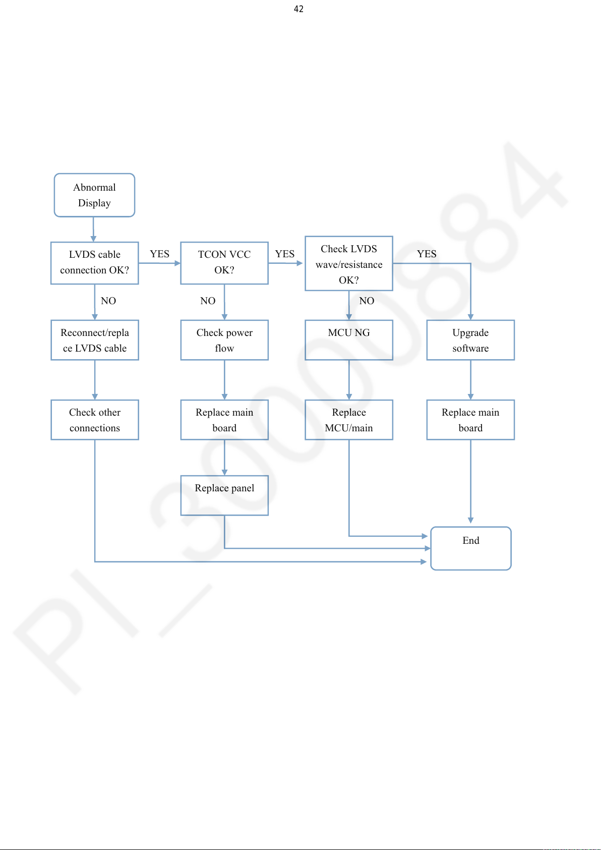
6.Abnormal Display
Abnormal
Display
LVDS cable
connection OK?
Reconnect/repla
ce LVDS cable
Check other
connections
TCON VCC
OK?
Check power
flow
Replace main
board
Check LVDS
wave/resistance
OK?
MCU NG
Replace
MCU/main
Upgrade
software
Replace main
board
Replace panel
End
42
OSD NG or picture NG.
YES YES YES
NO NO NO
Page 43

7.No tuning channels
No tuning
channels
Signal setting
OK?
Change setting/
tune again
Replace signal
source
Upgraded
software OK?
Check TV
settings
Tune again
Tuner power/
crystal/I2C bus
OK?
Check & replace
power flow/crystal units
Replace main
board
Replace tuner
IC/MCU
Replace main
board
End
43
DTV or ATV no Channels.
Page 44

Disassemble
44
The picture is from design model and may not 100 percent match the final end products,
but the operating process is the same. Make sure the wiring will remain the same
as you
open the TV set, wrong wiring may cause safety issue.
Disassemble process
Page 45

All electric parts need to handle with ESD measures, ESD glove/ wrist strip/ ESD
1. remove stand
2. remove back cover
45
workstation
is requested during repair process. And TV should place on an ESD cloth pad in case
of scratch
and crack during repair work. Use Rosh solder paste if you want to repair components.
The left and right side stand in the same, move 2 screws for each side stand.
Remove screws of back cover, remove the back cover,
Page 46

3. remove PCB
Pull out the socket connection in red block and remove screws in red circle. Take
4. remove IR/Key PCB
46
out the PCB.
You can find IR and key pad in the red box.
There is no screw on the IR board, untie the hook structure and take out the PCB.
Remove the key pad.
Specification
Brief look on the model
Page 47
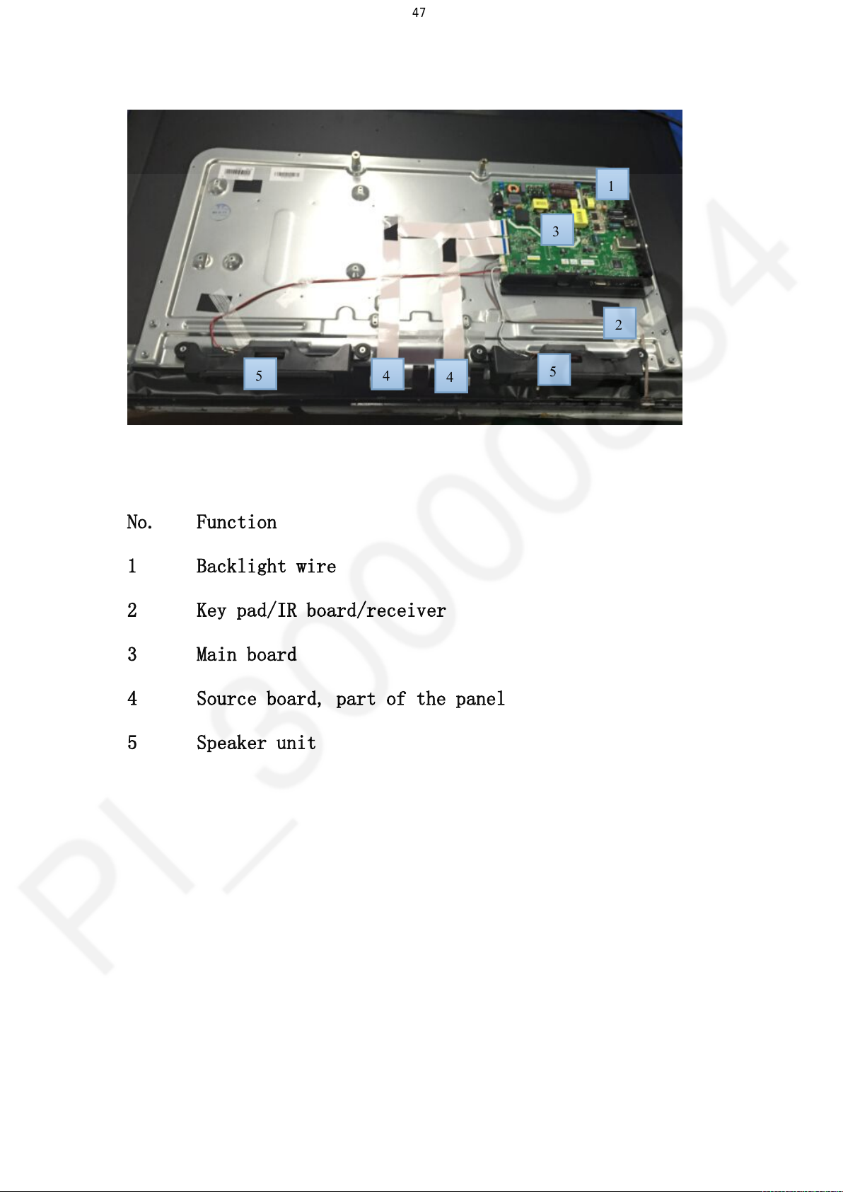
No. Function
1
234
4
5
5
47
No. Function
1 Backlight wire
2 Key pad/IR board/receiver
3 Main board
4 Source board, part of the panel
5 Speaker unit
Page 48

VESA assemble process
48
For smaller and medium flat panels, LCD monitors and screens from 12" to 22.9"
diagonal, and falling in a weight range up to 30.8 lbs. (14 kg): 75mm x 75 mm or
100 mm x 100 mm (2.95" x 2.95" or 3.94" x 3.94")
For larger monitors with viewing screen from 23" to 30.9" diagonally, weight range
up to 50 lbs.: VESA 200mm x 100mm and 200mm x 200mm
For large Plasma screens and LCD TV displays 31" to 90" diagonal, but weights
not greater than 250 lbs. there are various hole patterns in 200 mm increments:
400mm x 200mm, or 600mm x 400mm, or 800mm x 400mm
The above data is suggested specification; the standard accessory do not include a VESA, customer
need to purchase from out sources.
Step1, check and make sure the wall is strong enough to hold the TV.
Before assemble the VESA, make sure the wall is strong enough for TV. Some wall is
empty inner for cost down in house fitment, if in this condition you can only put TV on
table. The requested load force of wall must 4 times more than the TV weights.
After VESA assemble, the wall mast not tear down in 10 degrees’ slope from the TV.
Step2, check the environment of using condition
First comes the humidity, all TV cannot bear too much wetness. Especially the liquid
crystal screen and PCB inner TV model, water and dust/fiber may cause short circuit.
Second comes the sunlight, too much light/heat may speedup the liquid crystal and
plastic ageing. Third comes the distance, the best viewing distance for a TV set is 3-5
times from its size.
Step3, VESA selection
Though the LED TV is lighter from CRT, we still request to pick some strong structure.
Or we will pay a lot of lose in case of failure.
Page 49

49
Step4, VESA assemble
When the wall is different, the assemble process is different.
When it is bricks, insert expansion screws directly.
When it is gypsum board or wooden board, use a wooden stick between VESA and wall,
to spread the force to the wood stick touching surface to make safe.
Make marks with knife or mark pen on the wall, mount at least 6 expansion screws to
hold the VESA.
Step5, TV mount
Use the screws in accessory bag or from VESA supplier, mount the iron stick to TV set.
Put the TV on the wall with hook structure or combine TV to wall mount with screws.
Page 50

50
Page 51

IGP List
S/N Part Code Simplified Description Description Q'ty unit Model No Model Name
1 1002-QE200002-21 Back Cover B.CAB HIPS(94-V0) DG001 QE200000-PA2 43E 1 PC TH-43D310Q 43INCH TV
2
-01H43P210-S4
Main Board 5M53A-43P210(HI)MAIN BOARD ASEMBLE 1 PC TH-43D310Q 43INCH TV
3 7626-T4300L-Y48030 Panel 43" SKY-RGB LCD HNB003 RDL430FY(LD0-402) 1 PC TH-43D310Q 43INCH TV
4
-18H43P210-06 Reveiver Board 5M53A-43P210(HI)RECEIVER BOARD ASSEMBL 1 PC TH-43D310Q 43INCH TV
5 ST00-QP2100-W 0 Stand STAND PARTS P2100-A BASE HNB003 2 PC TH-43D310Q 43INCH TV
6 5631-106154-0070 Speaker SPEAKER 6 OHM 12W MAX 15W 236*37*47.5MM 2 PC TH-43D310Q 43INCH TV
A1 5942-A15205-1020 Power Cord AC LINE CORD 1500MM 0.75*2 BIG SOUTH AFR 1 PC TH-43D310Q 43INCH TV
A2 5900-F45131-5010 Left LVDS cable FFC 50 PINS P=0.5MM L=450MM(245+10*2+185 1 PC TH-43D310Q 43INCH TV
A3 5900-F35131-5020 Right LVDS cable FFC 50 PINS P=0.5MM L=350MM(220+15*2+100 1 PC TH-43D310Q 43INCH TV
A4 53HD-260401-W000 Remote Control Remote Control HS-0401P-00 "PANASONIC" FO 1 PC TH-43D310Q 43INCH TV
51
Page 52

S
5
W
L
u
52
52
BOM LIST
Part No. Description Q'ty Unit
4900-116052-R000 CRYSTAL 16.000000MHZ HC-49U/S CL:20PF +/ 1 PC
4900-124053-R000 CRYSTAL 24.000000MHZ HC-49U/S CL:20PF +/ 1 PC
5400-921120-0420 WAFER(M) P=2.0MM H-TYPE SINGLE ROW 4 PIN 1 PC
6100-020100-0450 EARPHONE JACK 3.5MM H-TYPE BLACK 1 PC
6100-049100-01C0 RF CONNECTOR (F) H-TYPE 14.2MM D=6.1MM 1 PC
6100-089110-0410 USB(AF) SOCKET H-TYPE 4 PINS (13.9*13*12 1 PC
6100-160110-0170 RCA JACK X 1 H-TYPE BLACK H=14.7MM 1 PC
6100-16F110-03D0 RCA JACK X 3 H-TYPE P=14MM (RED WHITE YE 1 PC
6100-260110-1510 VGA SOCKET H-TYPE 15 PINS W/SCREW 3
1505-P0140120-2102 HEAT SINK SPTE #P-01 W14*D12*H15.5mm 0.7 1 PC
4134-NJ0510-00 POWER THERMISTOR RESISTOR 5 OHM 4A +/-
4157-FK10B0-5T00 WIRE WOUND NON-INDUCTIVE RES. 0.1 OHM
4176-L68166-7Q10 VARISTOR 680V ±10% I(MAX)=6000A D=14MM ( 1 PC
4313-EN1050-7ZE0 M.P-P.F.CAP. 1UF 450V +/-10% (FORMED P=1 1 PC
432L-BG4773-ALA0 ELEC. CAP. 470UF 63V ±20% 12.5*20MM 105* 2 PC
432R-BD1083-AL00 ELEC. CAP. 1000UF 25V +/-20% 105*C HFLZ 2 PC
432R-BE4773-ARX0 ELECTROLYTIC CAPACITOR 470UF 35V +/-20% 1 PC
432R-BF1073-AZX0 ELEC. CAP. 100UF 50V +/-20% 105*C HFLZ 8 1 PC
4338-S21010-7Z20 SAFETY CERAMIC CAP. 100PF AC250V +/-10% 2 PC
4338-S51020-AZ20 SAFETY CERAMIC CAP. 1NF AC400V +/-20% (F 1 PC
4338-S54710-7Z20 SAFETY CERAMIC CAP. 470PF AC400V +/-10%( 2 PC
433X-DP2230-5Z40 POL
433X-F32240-7ZE0 AC CAPACITOR 220NF AC275V ±10%(P=15MMM,
433X-F34740-7R40 AC CAPACITOR 470NF AC275V +/-10% (R-FORM 1 PC
434E-BI6861-AR00 ELEC. CAP. 68UF 160V ±20% 10*20MM 105*C 2 PC
4380-BN6861-A040 ELEC. CAP. 68UF 450V ±20% 105*C 12.5*40M 2 PC
4522-154080-0Q50 NORMAL RECTIFIER DIODE 1N5408 3A/1000V D 4 PC
4522-2U4600-0Z50 HIGH SPEED RECTIFIER DIODE MUR460 600V/4 1 PC
47AH-P817C0-04 IC BPC-817C BRIGHT LED (PHOTOCOUPLER)) 1 PC
481Y-021010-7020 CHOKE COIL 100UH ±10% 8-4 PINS 2 PC
481Y-022510-70A0 PFC COIL 250UH ±10% 6-2 PINS 1 PC
4846-061830-Z010 AC LINE FILTER 18mH X 2(MIN) TOLERANCE≤0 1 PC
4852-061920-Z000 AC LINE FILTE
5157-06EQ26-0050 SWITCHING TRANSFORMER BCK-30-L02650
544N-921120-1010 WAFER(M) P=2.0MM H-TYPE SINGLE ROW 10 PI 1 PC
544N-921130-0220 WAFER(M) P=2.0MM V-TYPE SINGLE ROW 2 PIN 1 PC
544N-921130-0230 WAFER(M) P=2.5MM V-TYPE SINGLE ROW 2 PIN 1 PC
614C-120100-0220 AC POWER SOCKET(8) 2 TERMINAL H-TYPE 1 PC
5M53A-01AA00-K1 (AI) MAIN & POWER & DRIVER ASS'Y 5M53A-4 1 ST
168P-G4L015-AAK0 (AI) POWER ASS'Y 168P-G4L015-K0 1 ST
5M53A-01S43P210-
4300-BC1070-AT00 ELECTROLYTIC CAP 100UF 16V +/-20% 6.3*7M 2 PC
4300-BC2270-AT00 ELECTROLYTIC CAP 220UF 16V +/-20% 6.3*7M 5 PC
432R-BC2271-AT40 ELEC. CAP. 220UF 16V ±20% 105*C 6.3*7MM 1 PC
4338-AR1010-7T00 CER CAP 100PF 1KV +/-10% P=5MM TAPE 1 PC
4348-AR681D-T0 CERAMIC CAPACITOR 680PF 1KV +/-10%(TAPE 1 PC
4622-A10130-T0 TRANSISTOR 2SA1013 (TAPE TYPE) 6 PC
6014-D2021A-0T00 FUSE 2A/250V VDE/CQC/UL 8.4*7.2MM SQUARE 1 PC
6014-D3121A-0T00 FUSE 3.15A/250V VDE/CQC/UL 8.4*7.2MM SQU 1 PC
5M53A-01SA00-K1 (TI) MAIN & POWER & DRIVER ASS'Y 5M53A-4 1 ST
K15M53A-43P210(TI)MAIN BOARD ASEMBLE 1 ST
YPROPYLENE FILM CAP. 22NF 630V ±5% (F 1 PC
R 1.9mH X 2 (MIN) TOLERANCE 1 PC
ROW
1
5
500
1 PC
2 PC
1 PC
1 PC
1 PC
Page 53

168P-G4L015-SAK0 (TI) POWER ASS'Y 168P-G4L015-K0 1 ST
5M53A-01SB0X-K0 (TI) MAIN MATCH SCREEN ASS'Y 5M53A-43P21 1 ST
4100-CA0000-T0 SMD RESISTOR 0 OHM 1/10W +/-5% (1.6x0.8M 11 PC
4100-CA0000-T7 SMD RESISTOR 0 OHM 1/16W +/-5% ( 0402 1 13 PC
4100-CA0220-T0 SMD RESISTOR 2.2 OHM 1/10W +/-5% (1.6x0. 1 PC
4100-CA1010-T7 SMD RESISTOR 100 OHM 1/16W +/-5% ( 0402 13 PC
4100-CA1020-2200 SMD RESISTOR 1K OHM 1/16W +/-1% (1.0 X0. 2 PC
4100-CA1020-T7 SMD RESISTOR 1K OHM 1/16W +/-5% ( 0402 1 13 PC
4100-CA1030-2200 SMD RESISTOR 10K OHM 1/16W +/-1% TAPE TY 2 PC
4100-CA1030-T0 SMD RESISTOR 10K OHM 1/10W +/-5% (1.6x0. 1 PC
4100-CA1030-T7 SMD RESISTOR 10K OHM 1/16W +/-5% ( 0402 19 PC
4100-CA1040-T7 SMD RESISTOR 100K OHM 1/16W +/-5% (0402 7 PC
4100-CA1140-T1 SMD RESISTOR 110K OHM 1/10W +/-1% (1.6x0 1 PC
4100-CA1220-2200 SMD RESISTOR1.2K OHM 1/16W+/-1%(1.0X0.5X 1 PC
4100-CA1230-T7 SMD RESISTOR 12K OHM 1/16W +/-5% (0402 1 2 PC
4100-CA1240-T7 SMD RESISTOR 120K OHM 1/16W +/-5% (0402 1 PC
4100-CA1520-A1 SMD RESISTOR 1.5K OHM 1/10W +/-1% (1.6 X 1 PC
4100-CA1820-2200 SMD RESISTOR 1K8 OHM 1/16W +/-1% (1.0 X0 1 PC
4100-CA1832-2200 SMD RESISTOR 18K2 OHM 1/16W +/-1%(1.0*0. 1 PC
4100-CA2010-T7 SMD RESISTOR 200 OHM 1/16W +/-5% (0402 1 2 PC
4100-CA2020-T1 SMD RESISTOR 2K OHM 1/10W +/-1% (1.6 X 0 1 PC
4100-CA2030-T7 SMD RESISTOR 20K OHM 1/16W +/-5% (0402 1 1 PC
4100-CA2200-T0 SMD RESISTOR 22 OHM 1/10W +/-5% (1.6x0.8 4 PC
4100-CA2200-T7 SMD RESISTOR 22 OHM 1/16W +/-5% ( 0402 1 4 PC
4100-CA2210-T7 SMD RESISTOR 220 OHM 1/16W +/-5% (0402 1 4 PC
4100-CA2231-2200 SMD RESISTOR 22K1 OHM 1/16W +/-1% (1.0*0 1 PC
4100-CA2720-T7 SMD RESISTOR 2.7K OHM 1/16W +/-5% (0402 1 PC
4100-CA3300-T7 SMD RESISTOR 33 OHM 1/16W +/-5% (0402 1. 4 PC
4100-CA3340-T7 SMD RESISTOR 330K OHM 1/16W +/-5% (0402 3 PC
4100-CA4700-2200 SMD RESISTOR 47 OHM 1/16W +/-1% (1.0*0.5 4 PC
4100-CA4710-2200 SMD RESISTOR 470 OHM 1/16W +/-1% 1005 RO 1 PC
4100-CA4710-T0 SMD RESISTOR 470 OHM 1/10W +/-5% (1.6x0. 2 PC
4100-CA4720-T7 SMD RESISTOR 4.7K OHM 1/16W +/-5% ( 0402 15 PC
4100-CA4730-2200 SMD RESISTOR 47K OHM 1/16W +/-1% (1.0 X0 1 PC
4100-CA4730-T7 SMD RESISTOR 47K OHM 1/16W +/-5% (0402 1 1 PC
4100-CA4740-T7 SMD RESISTOR 470K OHM 1/16W +/-5% (0402 1 PC
4100-CA5120-T7 SMD RESISTOR 5.1K OHM 1/16W +/-5% (0402 1 PC
4100-CA5130-2200 SMD RESISTOR 51K OHM 1/16W +/-1% (1.0*0. 1 PC
4100-CA6800-T7 SMD RESISTOR 68 OHM 1/16W +/-5% (0402 1. 2 PC
4100-CA6820-T7 SMD RESISTOR 6.8K OHM 1/16W +/-5% ( 0402 1 PC
4100-CA7500-T7 SMD RESISTOR 75 OHM 1/16W +/-5% ( 0402 1 5 PC
4100-CA8220-2200 SMD RESISTOR 8K2 OHM 1/16W +/-1% (1.0 X 1 PC
4100-CA8220-T7 SMD RESISTOR 8.2K OHM 1/16W +/-5% (0402 1 PC
4100-CA9120-5200 SMD RESISTOR 9.1K OHM 1/16W +/-5%(1.0X0. 1 PC
4100-CA9120-T6 SMD RESISTOR 9.1K OHM 1/16W +/-1% (0402 1 PC
4100-CB0000-T0 SMD RESISTOR 0 OHM 1/8W +/-5% (0805 TYPE 2 PC
4100-CD27B0-2500 SMD RESISTOR 0R27 OHM 1/4W +/-1% (3.1*1. 1 PC
4100-JA0000-T2 SMD RESISTOR NETWORK (0 OHM X 4) 1/16W + 6 PC
4100-NJ4730-2200 SMD NTC THERMISTOR RESISTOR 47K OHM +/-
1
1 PC
4300-CA1060-A300 SMD CC CAP 10UF/6.3V +/-20% 1608 8 PC
4300-CA475D-T2 SMD CERAMIC CAPACITOR 4.7UF 6.3V+/-10 (T 1 PC
53
Page 54

4300-CB1050-A200 SMD X5R CERAMIC CHIP CAP. 1UF 10V +/-20% 5 PC
4300-CB2250-7300 SMD X5R CERAMIC CHIP CAP. 2U2F 10V +/-10 2 PC
4300-CB2250-A200 SMD X5R MLCC 2U2F 10V +/-20% (1.0*0.5MM) 2 PC
4300-CC104D-T5 SMD CERAMIC CHIP CAPACITOR 0.1UF 16V +/- 56 PC
4300-CC105D-T2 SMD CERAMIC CHIP CAPACITOR 1UF 16V +/-10 3 PC
4300-CC1060-7400 SMD X5R CERAMIC CHIP CAPACITOR 10UF
16V+
14 PC
4300-CC473D-T5 SMD CERAMIC CHIP CAPACITOR 0.047UF16V+/- 8 PC
4300-CD1050-7300 SMD X5R CERAMIC CHIP CAP. 1UF 25V +/-10% 6 PC
4300-CD223D-T5 SMD CERAMIC CHIP CAPACITOR 0.022UF 25V + 3 PC
4300-CD2250-A400 SMD X5R CERAMIC CHIP CAP.2U2F 25V +/-20% 1 PC
4300-CD2260-A500 SMD X5R CERAMIC CHIP CAP.22UF 25V +/-20% 11 PC
4300-CF102D-T5 SMD CERAMIC CHIP CAPACITOR 0.001UF 50V + 9 PC
4300-CF1030-7200 SMD X7R CERAMIC CHIP CAP. 10NF 50V +/-10 1 PC
4300-CF104D-T2 SMD CERAMIC CHIP CAPACITOR 0.1UF 50V +/- 7 PC
4300-CF1050-7400 SMD X7R CERAMIC CHIP CAP. 1UF 50V +/-10% 4 PC
4300-CF2220-7200 SMD X7R CERAMIC CHIP CAP. 2N2F 50V +/-10 1 PC
4300-CF224E-T2 SMD CERAMIC CHIP CAPACITOR 0.22UF 50V +/ 1 PC
4300-CF271C-T2 SMD CERAMIC CHIP CAPACITOR 270PF 50V +/- 1 PC
4300-CF331D-T5 SMD CERAMIC CHIP CAPACITOR 330PF 50V +/- 4 PC
4300-CF333D-T2 SMD CERAMIC CHIP CAPACITOR 0.033UF 50V + 4 PC
4300-CF472D-T5 SMD CERAMIC CHIP CAPACITOR 0.0047UF 50V 4 PC
4300-CF474D-T1 SMD C-CERAMIC,CHIP;470NF,+/-10%,50V,X7R, 4 PC
4300-NF150C-T5 SMD NPO CERAMIC CHIP CAPACITOR 15PF 50V 4 PC
4300-NF220C-T5 SMD NPO CERAMIC CHIP CAPACITOR 22PF 50V 3 PC
4300-NF330C-T5 SMD NPO CERAMIC CHIP CAPACITOR 33PF 50V 5 PC
4300-NF470C-T5 SMD NPO CERAMIC CHIP CAPACITOR 47PF 50V 4 PC
4300-NF4710-5200 SMD NPO CERAMIC CHIP CAP. 470PF 50V +/-5 8 PC
4303-CF10A0-K200 SMD MLCC 1PF 50V +/-0.1PF (1.0*0.5)TAPE 1 PC
4303-CF56A0-K200 SMD MLCC 5P6F 50V +/-0.1PF(1.0*0.5)TAPE 1 PC
4500-234031-T0 SMD SCHOTTKY BARRIER DIODE MBRA340T3
3A/
2 PC
4500-254001-T0 SMD SCHOTTKY BARRIER DIODE BAT54S
PACKAG
2 PC
4500-50V990-T0 SMD SWITCHING DIODE BAV99 (TAPE TYPE) 2 PC
4600-M23450-0S00 SMD TRANSISTOR ME2345A(-30V/-4.2A P-CHAN 1 PC
4600-T39040-T0 SMD BJTR NPN 40V SOT-23 8 PC
4600-T39060-T0 SMD BJTR PNP 40V SOT-23 ROHS 2 PC
4722-T57070-0480 SMD IC TAS5707PHPR TEXAS(20W STEREO
DIGI
1 PC
472L-R69191-0560 SMD IC RT6919CGQV RICHTEK (T-CON POWER) 1 PC
474R-G57280-0050 SMD IC G5728TO1U GMT(STEP-DOWN
REGULATOR
1 PC
4786-A30150-0080 SMD IC AOZ3015AI ALPHA (3A SYNCHRONOUS
B
1 PC
47B6-A11170-03 SMD IC AS1117L-3.3/TR-HF A1(3.3V/1A FIXE 2 PC
47B6-A11174-0300 SMD IC AS1117L/TR-HF A1(1A ADJUSTABLE LD 1 PC
47C4-M66100-0240 SMD IC MXL661 MAXLINEAR (SILICON TUNER) 1 PC
47D9-M94350-0080 SMD IC ME9435A MATSUKI (P-CHANNEL
MOSFET
1 PC
47F2-G25321-0080 SMD IC GD25Q32CSIG GD (32M BIT SERIAL FL 1 PC
4800-S033B0-7300 SMD CHIP COIL R33UH +/-10% (1.6 X 0.8MM) 1 PC
4800-S11000-AS80 SMD POWER INDUCTORS 10UH +/-20% 3.0A(6.0 1 PC
4800-S12200-7S00 SMD WIRE WOUND COIL 22UH +/-10% 2.2A (5. 4 PC
4800-S12200-AS80 SMD POWER INDUCTORS 22UH +/-20% 1.9A(6.0 2 PC
4800-S13320-AS00 SMD WIRE WOUND COIL 3U3H +/-20% 4.0A(5.2 1 PC
482J-S082D0-4200 SMD CHIP COIL 8.2NH +/-3% 380mA (1.0*0.5 1 PC
482J-S168A0-AS20 SMD POWER INDUCTORS 6R8 UH +/-20% 750MA 1 PC
54
Page 55

4876-2833C0-5200 SMD RF CERAMIC INDUCTOR 33NH +/-5%
200MA
2 PC
5400-99112S-0900 SMD WAFER(M) P=1.25MM H-TYPE SINGLE
ROW
1 PC
5800-A5M53A-0P00-C MAIN & POWER & DRIVER PCB 210*188*1.6MM 1 PC
6000-300001-00 SMD FUSE 3A/32V (VERY FAST-ACTING) 1 PC
6000-500429-T0 SMD FUSE 5A/32V FAST TIME-TO-TRIP UL/CSA 1 PC
6100-150110-1940 SMD HDMI SOCKET BLACK H-TYPE 19 PIN FOR8 2 PC
6400-011102-T0 SMD FERRITE BEAD (1.6 X 0.8 X 0.8MM) Z=1 1 PC
6400-011121-T0 SMD MC BEAD Z=120 OHM+/-25%@100MHZ 0.6A 5 PC
6400-011600-T0 SMD FERRITE BEAD (1.6 X 0.8MM) TAPE TYPE 3 PC
6400-011608-T0 SMD FERRITE BEAD (1.6 X 0.8MM) TAPE TYPE 1 PC
475C-T56RU1-1280 SMD IC TSUMV56RUET-0051 MSTAR (TV
CONTRO
1 PC
4500-50V700-T0 SMD SWITCHING DIODE BAV70 (TAPE TYPE) 1 PC
4600-N70020-T0 SMD TRANSISTOR 2N7002 N-CHANNEL MOSFET
S
2 PC
4876-S022B0-5220 SMD CHIP COIL 220NH +/-5% 100MA (1.0*0.5 2 PC
4144-CA0000-T0 SMD RESISTOR 0 OHM 1/10W +/-5% 1608 TAPE 10 PC
4144-CA0220-T0 SMD RESISTOR 2.2 OHM 1/10W +/-5% (1.6X0. 1 PC
4144-CA0470-T7 SMD RESISTOR 4.7 OHM 1/16W +/-5% ( 0402 6 PC
4144-CA0510-T0 SMD RESISTOR 5.1 OHM 1/10W +/-5% (1.6 X0 1 PC
4144-CA1000-T0 SMD RESISTOR 10 OHM 1/10W +/-5% 1608 TAP 17 PC
4144-CA1010-T0 SMD RESISTOR 100 OHM 1/10W +/-5% 1608 TA 1 PC
4144-CA1020-T0 SMD RESISTOR 1K OHM 1/10W +/-5% 1608 TAP 3 PC
4144-CA1030-T0 SMD RESISTOR 10K OHM 1/10W +/-5% 1608 TA 5 PC
4144-CA1030-T1 SMD RESISTOR 10K OHM 1/10W +/-1% 1608 TA 1 PC
4144-CA1040-T0 SMD RESISTOR 100K OHM 1/10W +/-5% 1608 T 2 PC
4144-CA1240-T0 SMD RESISTOR 120K OHM 1/10W +/-5% 1608 T 1 PC
4144-CA1632-T1 SMD RESISTOR 16.2K OHM 1/16W +/-1% 1608 1 PC
4144-CA1820-T0 SMD RESISTOR 1.8K OHM 1/10W +/-5% (1.6x0 1 PC
4144-CA1830-T0 SMD RESISTOR 18K OHM 1/10W +/-5% 1608 TA 1 PC
4144-CA2020-T0 SMD RESISTOR 2K OHM 1/10W +/-5% (1.6x0.8 3 PC
4144-CA2030-T0 SMD RESISTOR 20K OHM 1/10W +/-5% 1608 TA 3 PC
4144-CA2030-T1 SMD RESISTOR 20K OHM 1/10W +/-5% (1.6 X0 1 PC
4144-CA2200-T0 SMD RESISTOR 22 OHM 1/10W +/-5% 1608 TAP 3 PC
4144-CA2220-T0 SMD RESISTOR 2.2K OHM 1/10W +/-5% 1608 T 1 PC
4144-CA3330-T0 SMD RESISTOR 33K OHM 1/10W +/-5% (1.6x0. 2 PC
4144-CA4720-T1 SMD RESISTOR 4.7K OHM 1/10W +/-1% (0603 3 PC
4144-CA4730-T0 SMD RESISTOR 47K OHM 1/10W +/-5% 1608 TA 2 PC
4144-CA4740-T0 SMD RESISTOR 470K OHM 1/10W +/-5% (1.6X0 1 PC
4144-CA5120-T0 SMD RESISTOR 5.1K OHM 1/10W +/-5% (1.6x0 7 PC
4144-CA5130-T0 SMD RESISTOR 51K OHM 1/10W +/-5% 1608 TA 1 PC
4144-CA5620-T0 SMD RESISTOR 5.6K OHM 1/10W +/-5% (1.6x0 1 PC
4144-CA6800-T0 SMD RESISTOR 68 OHM 1/10W +/-5% (1.6x0.8 1 PC
4144-CA6820-T0 SMD RESISTOR 6.8K OHM 1/10W +/-5% 1608 T 1 PC
4144-CB1230-2400 SMD RESISTOR 12K OHM 1/8W +/-1% (2.0 X 1 1 PC
4144-CB2740-2400 SMD RESISTOR 270K OHM 1/8W +/-1% 2012 TA 2 PC
4144-CB43A0-2400 SMD RES.4R3 OHM 1/8W 6 PC
4144-CB6800-T0 SMD RESISTOR 68 OHM 1/8W +/-5% 2012 TAPE 3 PC
4144-CD1000-00 SMD RESISTOR 10 OHM 1/4W +/-5% 3216 TAPE 2 PC
4144-CD1020-T0 SMD RESISTOR 1K OHM 1/4W +/-5% 3216 TAPE 1 PC
4144-CD1050-T0 SMD RESISTOR 1M OHM 1/4 W +/-5% 3216 TAP 2 PC
4144-CD1550-2500 SMD RESISTOR 1M5 OHM 1/4W +/-1% (3.2*1.6 5 PC
4144-CD27B0-2500 SMD RESISTOR 0.27 OHM 1/4W +/-1% 3216 TA 3 PC
55
Page 56

4144-CD3930-2500 SMD RESISTOR 39K OHM 1/4W +/-1% (3.2 X 1 1 PC
4144-CD4740-T1 SMD RESISTOR 470K 1/4W +/-1% (1206 3.2X 4 PC
4144-CD5140-T1 SMD RESISTOR 510K OHM 1/4W +/-1 3216 TAP 2 PC
4144-CD8240-5500 SMD RESISTOR 820K OHM 1/4W +/-5% 3216 TA 1 PC
4144-CY2040-2300 SMD RESISTOR 200K OHM 1/10W +/-1% (1.6*0 1 PC
431R-CC473D-T5 SMD X7R CERAMIC CHIP CAPACITOR 0.047UF16 1 PC
431R-CF1030-7200 SMD X7R CERAMIC CHIP CAPACITOR 10NF 50V 1 PC
431R-CF472D-T5 SMD X7R CERAMIC CHIP CAPACITOR 0.0047UF 1 PC
431R-NF101C-T5 SMD C0G CERAMIC CHIP CAPACITOR 100PF
50V
1 PC
433G-NT1010-5500 SMD NPO CERAMIC CAPACITOR 100PF 2KV +/-5 2 PC
4391-CA475D-T2 SMD X7R CERAMIC CHIP CAPACITOR 4.7UF 6.3 1 PC
4391-CC225D-T1 SMD X7R CERAMIC CHIP CAPACITOR 2.2UF 16V 3 PC
4391-CC474D-T2 SMD X7R CERAMIC CHIP CAPACITOR 0.47UF 16 3 PC
4391-CF104D-T1 SMD X7R CERAMIC CHIP CAPACITOR 0.1UF 50V 5 PC
4391-CF104D-T2 SMD X7R CERAMIC CHIP CAPACITOR 0.1UF 50V 10 PC
4391-CF1050-7400 SMD X7R CERAMIC CHIP CAPACITOR 1UF 50V + 1 PC
4391-CF224E-T2 SMD CERAMIC CHIP CAPACITOR 0.22UF 50V +/ 2 PC
4391-CF331D-T5 SMD X7R CERAMIC CHIP CAPACITOR 330PF 50V 3 PC
4391-CF333D-T1 SMD X7R CERAMIC CHIP CAPACITOR 0.033UF 5 1 PC
451F-220200-0S10 SMD SCHOTTKY RECTIFIER DIODE HBR20200
20
2 PC
451F-220450-0S00 SMD SCHOTTKY DIODE MBR2045S 45V/20A TO-
2
1 PC
4522-2S3MB0-0S00 SMD DIODE 1000V/3A 4.3*2.3mm DO-214AA(SM 2 PC
4522-2US1J0-0S10 SMD DIODE 600V/1A 4.3*2.6mm SMA TAPE TYP 6 PC
4522-400220-S5 SMD ZENER DIODE 22V 1/2W +/-5% ZMM22 3.5 3 PC
4522-400270-T1 SMD ZENER DIODE 27V 1/2W TAPE TYPE 2 PC
4522-401530-3S00 SMD ZENER DIODE 15V +/-2% 500MW SOD-123 1 PC
4522-402730-3S00 SMD ZENER DIODE 27V +/-2% 500mW SOD-123 1 PC
4522-404730-3S00 SMD ZENER DIODE 47V +/-2% 500MW SOD-123 1 PC
4522-431051-T0 SMD ZENER DIODE 5V1 1/4W +/-5% 2 PINS (T 1 PC
4522-54148F-0S00 SMD SWITCHING DIODE 1N4148W 0.3A/100V SO 6 PC
4555-400470-S5 SMD ZENER DIODE 47V 1/2W +/-5% ZMM47 3.5 1 PC
4601-T14G65-0S00 SMD TRANSISTOR TK14G65W (650V/13.7A N-CH 1 PC
4655-A9N500-0S00 SMD TRANSISTOR AOD9N50 (500V/9A,N-
CHANNE
2 PC
4661-T39040-T0 SMD BJTR NPN 40V SOT-23 2 PC
4666-P20150-0S00 SMD TRANSISTOR ME20N15-G(150V/20.8A,N-CH 1 PC
4706-T17160-0240 SMD IC TEA1716T NXP(PFC CONTROLLER)SO24 1 PC
476A-M33731-0280 SMD IC MP3373GM-Z MPS (8-STRING STEP-UP 1 PC
47B6-A43101-0030 SMD IC AS431AHM/TR-LF A1(ADJUSTABLE
PREC
1 PC
4871-310100-T0 SMD CHIP COIL 1UH +/-5%(3.2*1.6MM)TAPE T 1 PC
6018-B5012B-0300 SMD FUSE 0.5A/32V FAST TIME-TO-TRIP UL 1 1 PC
4144-CA1230-T1 SMD RESISTOR 12K OHM 1/10W +/-1% (1.6x0. 1 PC
4144-CB56A0-2400 SMD RESISTOR 5.6 OHM 1/8W +/-1% 2012 TAP 6 PC
5400-9A412S-5020 SMD FPC CONNECTOR P=0.5MM H-TYPE
SINGLE
2 PC
56
 Loading...