

Panasonic TH-42PX20U-P Service manual
V
V
A
ORDER NO. ITD0309035C1
High Definition Plasma Television
TH-42PX20U-P
GPH6DU Chassis
Specifications
Power Source AC 120 V, 50/60 Hz
Power Consumption Maximum :595 W
Stand-by condition :0.9 W
Plasma Displ ay panel Drive method :AC type 42-inch, 16 :9 aspect ratio
Screen Size 36.22 “ (920 mm) (W) × 20.39 “ (518 mm) (H) × 41.57 “ (1056 mm) (diagonal)
Dimensions
(W × H × D )
Mass (Weight) 90.4 lb.(41 kg)Net
Channel Capability-181 VHF-12 :UHF-56 :Cable-125
Sound
Speaker Woofer 80mm × 2 , Tweeter 16mm × 73mm × 8
Audio Output 26W[5W+5W,8W+8W](10%THD)
Headphone M3 (3.5 mm) Jack × 1
FEATURES Two screen display fuctions 3D Y/C FILTER
Accessories Supplied Remote control Transmitter EUR7603ZB0
Operating Conditions Temperature : 34 °F - 104 °F (0° - 40°C)
Connection Terminals RGB input D-SUB 15pin R, G, B /0.7 Vp-p (759)
44.88 “ (1140mm) × 29.8 “ (757 mm) × 5.47 “ (139 mm)
BBE VIVA LINEAR PIP
CLOSED CAPTION
AA Battery × 2 Ferrite cores (large × 5, small × 5)
AC Cord F type Antenna Adaptor (3C-2V × 2, 5C-2V × 2)
Pedestal
Humidity : 20 % - 80 % (non-condensing)
AV INPUT 1-3
-Chip
IDEO
(Phono Jack Type)
S-VIDEO
(Mini DIN 4-pin)
UDIO L-R
(Phono Jack Type × 2)
HD, VD /1.0 -5.0 Vp-p (high impedance)
1.0 Vp-p (759 )
Y :1.0 Vp-p (759), C : 0.286 Vp-p
(759)
0.5 Vrms
B19 Canada: B07
© 2003 Matsushita Electric Industrial Co., Ltd. All
rights reserved. Unauthorized copying and
distribution is a violation of law.

V
A
A
A
A
TH-42PX20U-P
Note:
AV PROG.OUT
TO AUDIO AMP
COMPONENT VIDEO Y 1.0 Vp-p (including synchronization)
INPUT1-2 PB /PR ±0.35Vp-p
HDMI INPUT HDMI type A connector
Design and Specifications are subject to change without notice.Weight and Dimensions shown are approximate.
IDEO
(Phono Jack Type)
UDIO L-R
(Phono Jack Type × 2)
UDIO L-R
(Phono Jack Type × 2)
UDIO L-R
(Phono Jack Type × 2)
UDIO L-R
(Phono Jack Type × 2)
1.0 Vp-p (759 )
0.5 Vrms
0.5 Vrms
0.5 Vrms
0.5 Vrms
CONTENTS
1 Applicable signals 4
2 Safety Precautions
2.1. General Guidelines
3 Prevention of Electro Static Discharge (ESD) to
Electrostatically Sensitive (ES) Devices
4 About lead free solder (PbF)
5 Service Hint
6 Location of Lead Wiring
6.1. Lead of Wiring (1)
6.2. Lead of Wiring (2)
6.3. Lead of Wiring (3)
6.4. Lead of Wiring (4)
6.5. Lead of Wiring (5)
6.6. Lead of Wiring (6)
7 Self-c heck Function
7.1. Self-check of the microcomputer control system (bus line)
7.2. Power LED Blinking timing chart
7.3. No Power
7.4. No Picture
7.5. Local screen failure
8 Serviceman Mode (Electronic Controls)
9 CAT (computer Aided Test) mode
9.1. IIC mode
9.2. CD mode
9.3. SD mode
9.4. IIC mode structure (following items value is sample data.)
10 Adjustment Procedure
Page Page
5
5
6
7
11 Adjustment
8
9
9
10
11
12 Hotel mode
12
13 Conductor Views
13
14
15
15
16
17
18
18
19
21
21
22
22
23
24
13.10. C2-Board
13.11. C3-Board
13.12. C4-Board
13.13. SC-Board
13.14. SU-Board
13.15. SD-Board
13.16. SS, SS2 and SS3-Board
13.17. JG-Board
10.1. Driver Set-up
10.2. Initialization Pulse Adjust
10.3. P.C.B. (Printed Circuit Board) exchange
10.4. Adjustment Volume Location
10.5. Test Point Location
11.1. Pedestal setting
11.2. NTSC panel white balance
11.3. HD panel white balance
11.4. Sub brightness setting
13.1. PF-Board
13.2. P-Board
13.3. PA-Board
13.4. TA and TB-Board
13.5. H-Board
13.6. DV-Board
13.7. DG-Board
13.8. D-Board
13.9. C1-Board
24
25
26
26
26
27
27
28
29
30
31
33
33
34
36
38
39
40
42
44
47
48
49
50
51
54
55
56
58
2

13.18. G-Board 60
13.19. K and S-Board
14 Block and Schematic Diagrams
14.1. Schematic Diagram Notes
14.2. Main Block Diagram
14.3. PF-Board Block Diagram
14.4. PF-Board Schematic Diagram
14.5. P-Board Block Diagram
14.6. P-Board (1 of 6) Schematic Diagram
14.7. P-Board (2 of 6) Schematic Diagram
14.8. P-Board (3 of 6) Schematic Diagram
14.9. P-Board (4 of 6) Schematic Diagram
14.10. P-Board (5 of 6) Schematic Diagram
14.11. P-Board (6 of 6) Schematic Diagram
14.12. PA and G-Board Block Diagram
14.13. PA-Board (1 of 3) Schematic Diagram
14.14. PA-Board (2 of 3) Schematic Diagram
14.15. PA-Board (3 of 3) Schematic Diagram
14.16. G-Board Schematic Diagram
14.17. TA, TB and H-Board Block Diagram
14.18. TA and TB-Board Schematic Diagram
14.19. H-Board (1 of 2) Schematic Diagram
14.20. H-Board (2 of 2) Schematic Diagram
14.21. DV-Board Block Diagram
14.22. DV-Board (1 of 3) Schematic Diagram
14.23. DV-Board (2 of 3) Schematic Diagram
14.24. DV-Board (3 of 3) Schematic Diagram
14.25. JG-Board Block Diagram
14.26. JG-Board (1 of 5) Schematic Diagram
14.27. JG-Board (2 of 5) Schematic Diagram
14.28. JG-Board (3 of 5) Schematic Diagram
14.29. JG-Board (4 of 5) Schematic Diagram
14.30. JG-Board (5 of 5) Schematic Diagram
14.31. DG-Board Block Diagram
14.32. DG-Board (1 of 7) Schematic Diagram
14.33. DG-Board (2 of 7) Schematic Diagram
14.34. DG-Board (3of 7) Schematic Diagram
14.35. DG-Board (4 of 7) Schematic Diagram
14.36. DG-Board (5 of 7) Schematic Diagram
14.37. DG-Board (6 of 7) Schematic Diagram
14.38. DG-Board (7 of 7) Schematic Diagram
14.39. D-Board (1 of 2) Block Diagram
14.40. D-Board (2 of 2) Block Diagram
14.41. D-Board (1 of 15) Schematic Diagram
14.42. D-Board (2 of 15) Schematic Diagram
100
101
102
103
104
14.43. D-Board (3 of 15) Schematic Diagram
61
63
63
64
65
66
67
68
69
70
71
72
73
74
75
76
77
78
79
80
81
82
83
84
85
86
87
88
89
90
91
92
93
94
95
96
97
98
99
14.44. D-Board (4 of 15) Schematic Diagram
14.45. D-Board (5 of 15) Schematic Diagram
14.46. D-Board (6 of 15) Schematic Diagram
14.47. D-Board (7 of 15) Schematic Diagram
14.48. D-Board (8 of 15) Schematic Diagram
14.49. D-Board (9 of 15) Schematic Diagram
14.50. D-Board (10 of 15) Schematic Diagram
14.51. D-Board (11 of 15) Schematic Diagram
14.52. D-Board (12 of 15) Schematic Diagram
14.53. D-Board (13 of 15) Schematic Diagram
14.54. D-Board (14 of 15) Schematic Diagram
14.55. D-Board (15 of 15) Schematic Diagram
14.56. C1, C2, C3, C4 and K-Board Block Diagram
14.57. C1-Board (1 of 2) Schematic Diagram
14.58. C1-Board (2 of 2) Schematic Diagram
14.59. C2-Board (1 of 2) Schematic Diagram
14.60. C2-Board (2 of 2) Schematic Diagram
14.61. C3-Board (1 of 2) Schematic Diagram
14.62. C3-Board (2 of 2) Schematic Diagram
14.63. C4-Board (1 of 2) Schematic Diagram
14.64. C4-Board (2 of 2) Schematic Diagram
14.65. S and K-Board Schematic Diagram
14.66. SC-Board Block Diagram
14.67. SC-Board (1 of 2) Schematic Diagram
14.68. SC-Board (2 of 2) Schematic Diagram
14.69. SU-Board Block Diagram
14.70. SU-Board (1 of 2) Schematic Diagram
14.71. SU-Board (2 of 2) Schematic Diagram
14.72. SD-Board Block Diagram
14.73. SD-Board (1 of 2) Schematic Diagram
14.74. SD-Board (2 of 2) Schematic Diagram
14.75. SS, S, SS2 and SS3-Board Block Diagram
14.76. SS-Board (1 of 2) Schematic Diagram
14.77. SS, SS2 and SS3-Board Schematic Diagram
15 Parts Location
15.1. Parts Location (1)
15.2. Parts Location (2)
15.3. Parts Location (3)
15.4. Parts Location (4)
15.5. Parts Location (5)
16 Mechanical Replacement Parts List
17 Replacement Parts List
17.1. Replacement Parts List Notes
17.2. Electrical Replacement Parts List
TH-42PX20U-P
105
106
107
108
109
110
111
112
113
114
115
116
117
118
119
120
121
122
123
124
125
126
127
128
129
130
131
132
133
134
135
136
137
138
139
141
141
142
143
144
145
146
147
147
148
3
TH-42PX20U-P
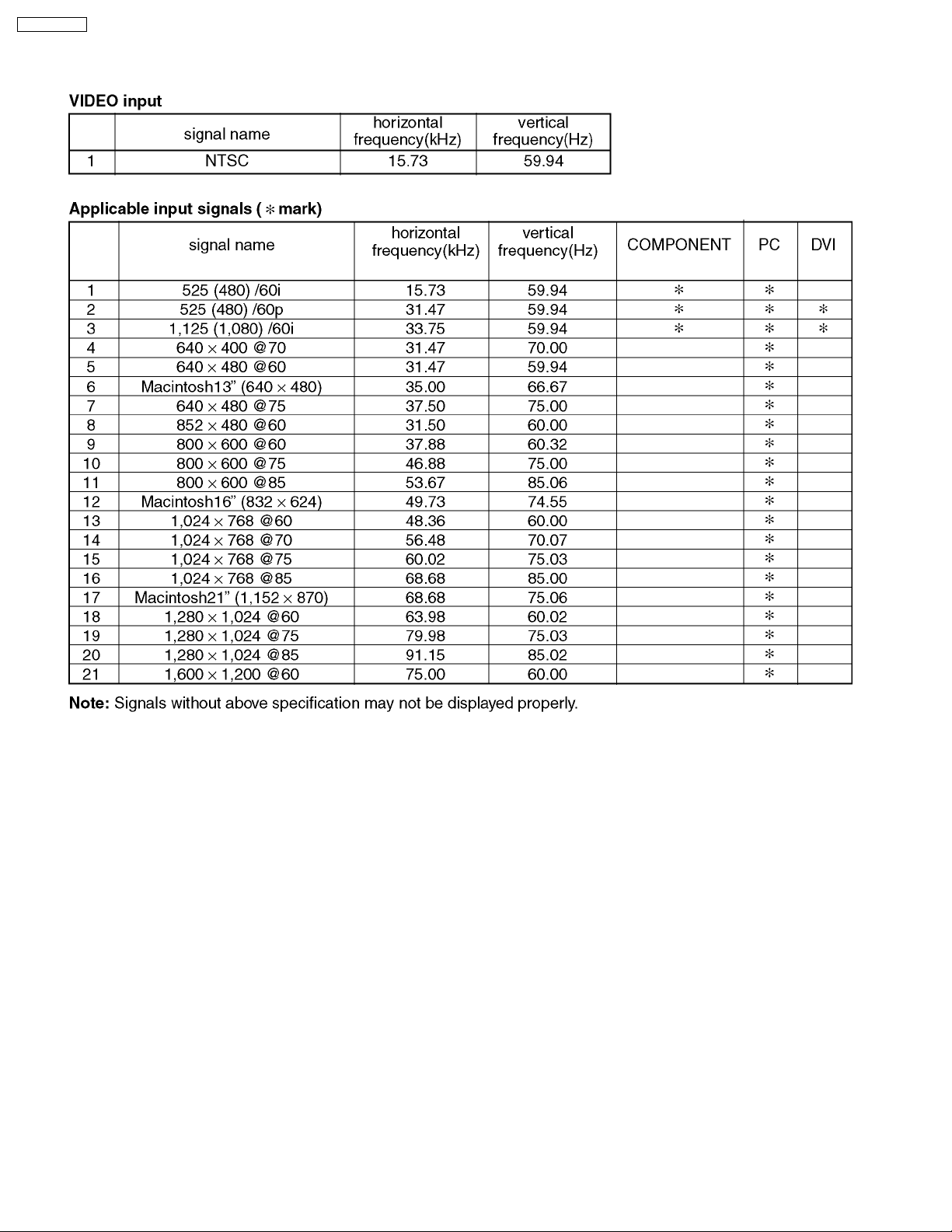
1 Applicable signals
4
2 Safety Precautions
2.1. General Guidelines
1.When servicing, observe the original lead dress. If a short circuit is found, replace all parts which have been overheated or
damaged by the short circuit.
2.After servicing, see to it that all the protective devices such as insulation barriers, insulation papers shields are properly
installed.
3.After servicing, make the following leakage current checks to prevent the customer from being exposed to shock hazards.
2.1.1. Leakage Current Cold Check
1.Unplug the AC cord and connect a jumper between the two
prongs on the plug.
2.Measure the resistance value, with an ohmmeter, between
the jumpered AC plug and each exposed metallic cabinet
part on the equipment such as screwheads, connectors,
control shafts, etc. When the exposed metallic part has a
return path to the chassis, the reading should be between
1M9 and 5.2M9.
When the exposed metal does not have a return path to
the chassis, the reading must be
.
TH-42PX20U-P
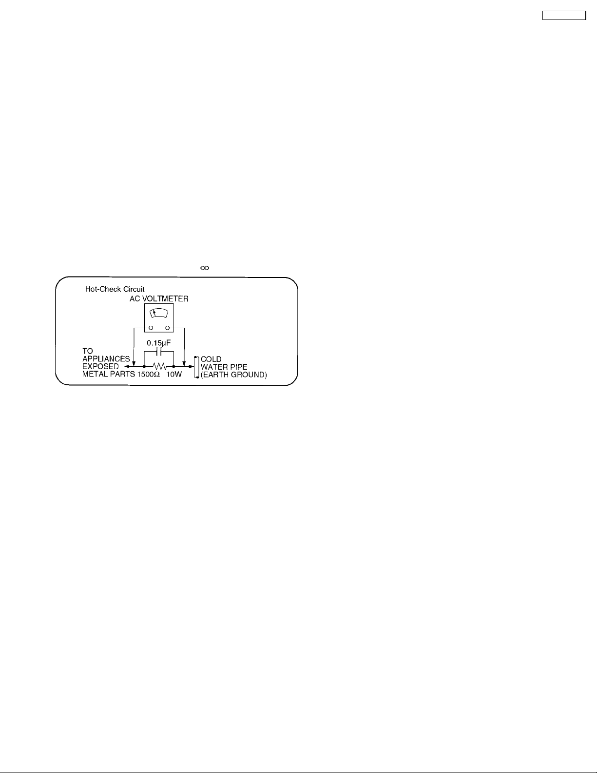
Figure 1
2.1.2. Leakage Current Hot Check (See
Figure 1.)
1.Plug the AC cord directly into the AC outlet. Do not use an
isolation transformer for this check.
2.Connect a 1.5k9, 10 watts resistor, in parallel with a 0.15µF
capacitors, between each exposed metallic part on the set
and a good earth ground such as a water pipe, as shown in
Figure 1.
3.Use an AC voltmeter, with 1000 ohms/volt or more
sensitivity, to measure the potential across the resistor.
4.Check each exposed metallic part, and measure the
voltage at each point.
5.Reverse the AC plug in the AC outlet and repeat each of the
above measurements.
6.The potential at any point should not exceed 0.75 volts
RMS. A leakage current tester (Simpson Model 229 or
equivalent) may be used to make the hot checks, leakage
current must not exceed 1/2 milliamp. In case a
measurement is outside of the limits specified, there is a
possibility of a shock hazard, and the equipment should be
repaired and rechecked before it is returned to the
customer.
5
TH-42PX20U-P
3 Prevention of Electro Static Discharge (ESD) to
Electrostatically Sensitive (ES) Devices
Some semiconductor (solid state) devices can be damaged easily by static electricity. Such components commonly are called
Electrostatically Sensitive (ES) Devices. Examples of typical ES devices are integrated circuits and some field-effect transistors and
semiconductor "chip" components. The following techniques should be used to help reduce the incidence of component damage
caused by electro static discharge (ESD).
1.Immediately before handling any semiconductor component or semiconductor-equipped assembly, drain off any ESD on your
body by touching a known earth ground. Alternatively, obtain and wear a commercially available discharging ESD wrist strap,
which should be removed for potential shock reasons prior to applying power to the unit under test.
2.After removing an electrical assembly equipped with ES devices, place the assembly on a conductive surface such as alminum
foil, to prevent electrostatic charge buildup or exposure of the assembly.
3.Use only a grounded-tip soldering iron to solder or unsolder ES devices.
4.Use only an anti-static solder removal device. Some solder removal devices not classified as "anti-static (ESD protected)" can
generate electrical charge sufficient to damage ES devices.
5.Do not use freon-propelled chemicals. These can generate electrical charges sufficient to damage ES devices.
6.Do not remove a replacement ES device from its protective package until immediately before you are ready to install it. (Most
replacement ES devices are packaged with leads electrically shorted together by conductive foam, alminum foil or comparable
conductive material).
7.Immediately before removing the protective material from the leads of a replacement ES device, touch the protective material
to the chassis or circuit assembly into which the device will be installed.
Caution
Be sure no power is applied to the chassis or circuit, and observe all other safety precautions.
8.Minimize bodily motions when handling unpackaged replacement ES devices. (Otherwise hamless motion such as the brushing
together of your clothes fabric or the lifting of your foot from a carpeted floor can generate static electricity (ESD) sufficient to
damage an ES device).
6
TH-42PX20U-P
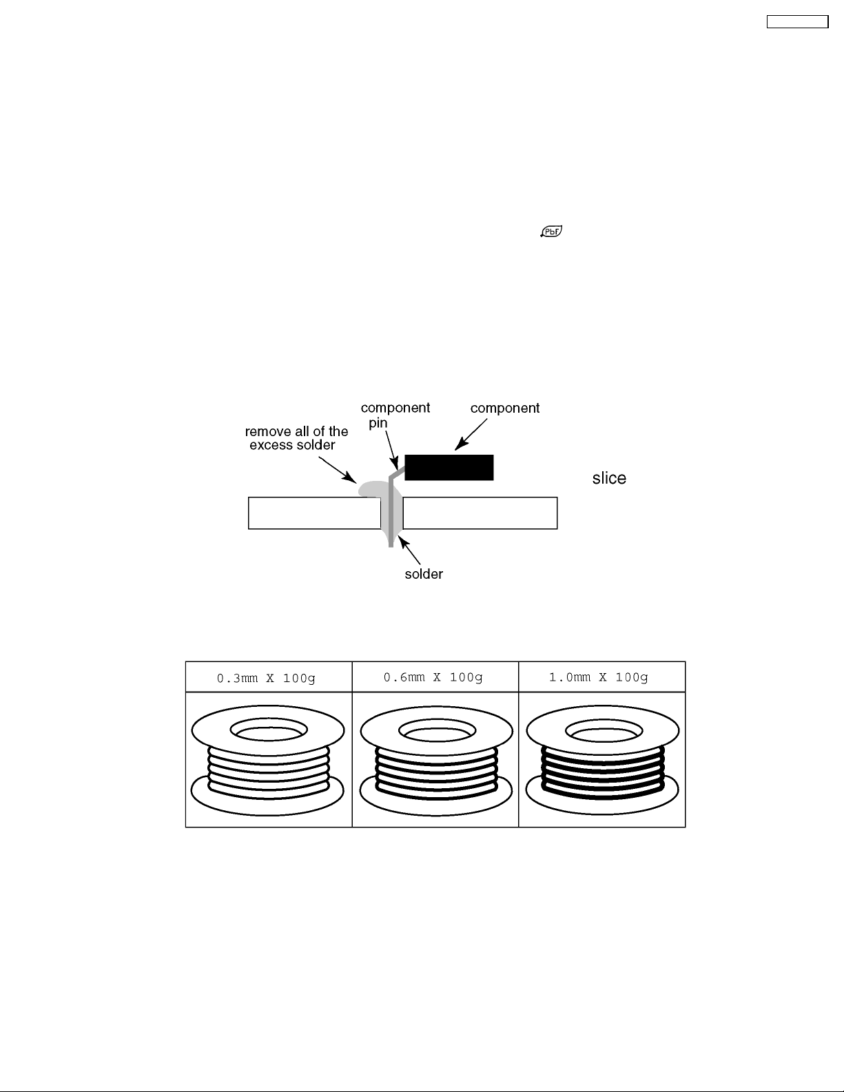
4 About lead free solder (PbF)
Note: Lead is listed as (Pb) in the periodic table of elements.
In the information below, Pb will refer to Lead solder, and PbF will refer to Lead Free Solder.
The Lead Free Solder used in our manufacturing process and discussed below is (Sn+Ag+Cu).
That is Tin (Sn), Silver (Ag) and Copper (Cu) although other types are available.
This model uses Pb Free solder in it’s manufacture due to environmental conservation issues. For service and repair work, we’d
suggest the use of Pb free solder as well, although Pb solder may be used.
PCBs manufactured using lead free solder will have the PbF within a leaf Symbol
Caution
·Pb free solder has a higher melting point than standard solder. Typically the melting point is 50 ~ 70 °F (30~40 °C) higher.
Please use a high temperature soldering iron and set it to 700 ± 20 °F (370 ± 10 °C).
·Pb free solder will tend to splash when heated too high (about 1100 °F or 600 °C).
If you must use Pb solder, please completely remove all of the Pb free solder on the pins or solder area before applying Pb
solder. If this is not practical, be sure to heat the Pb free solder until it melts, before applying Pb solder.
·After applying PbF solder to double layered boards, please check the component side for excess solder which may flow onto
the opposite side. (see figure below)
Suggested Pb free solder
There are several kinds of Pb free solder available for purchase. This product uses Sn+Ag+Cu (tin, silver, copper) solder.
However, Sn+Cu (tin, copper), Sn+Zn+Bi (tin, zinc, bismuth) solder can also be used.
stamped on the back of PCB.
7
TH-42PX20U-P
5 Service Hint
Board Name Function Board Name Function
C1 DATA DRIVER (UPPER RIGHT) PF LINE FILTER
C2 DATA DRIVER (UPPER LEFT) SC SCAN DRIVE
D DIGTAL SIGINAL PROCESS SD SCAN OUT (DOWN)
DG DIGTAL CORE MICOM SS SUSTAIN DRIVE
G FRONT TERMINAL, SWITCH SS2 SUSTAIN CONNECTION (UP)
H REAE TERMINAL SS3 SUSTAIN CONNECTION (DOWN)
K LED, REMOTE, SU SCAN OUT (UP)
P POWER SUPPLY TA MAIN TUNER
PA DC/DC, AUDIO TB SUB TUNER
C3 DATA DRIVER (LOWER RIGHT) JG PC/SD CARD
C4 DATA DRIVER (LOWER LEFT) DV HDMI
S POWER SW
8

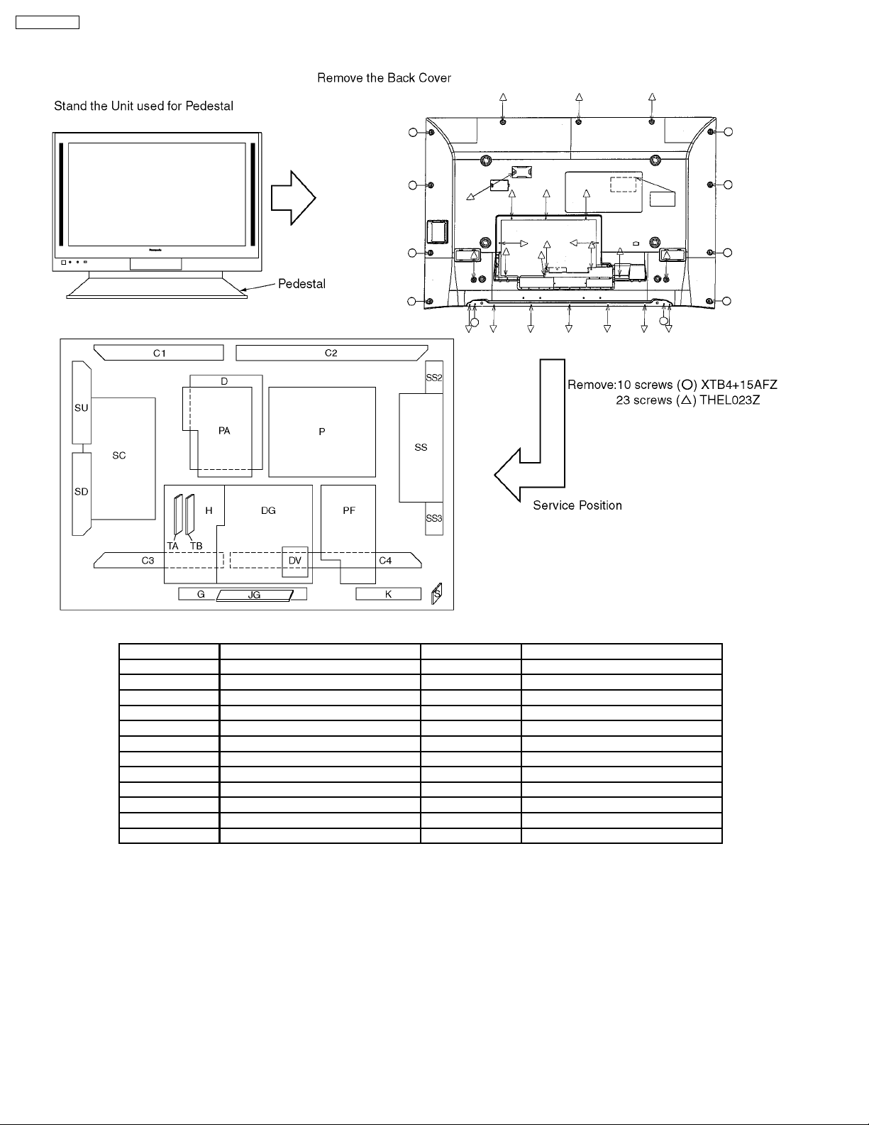
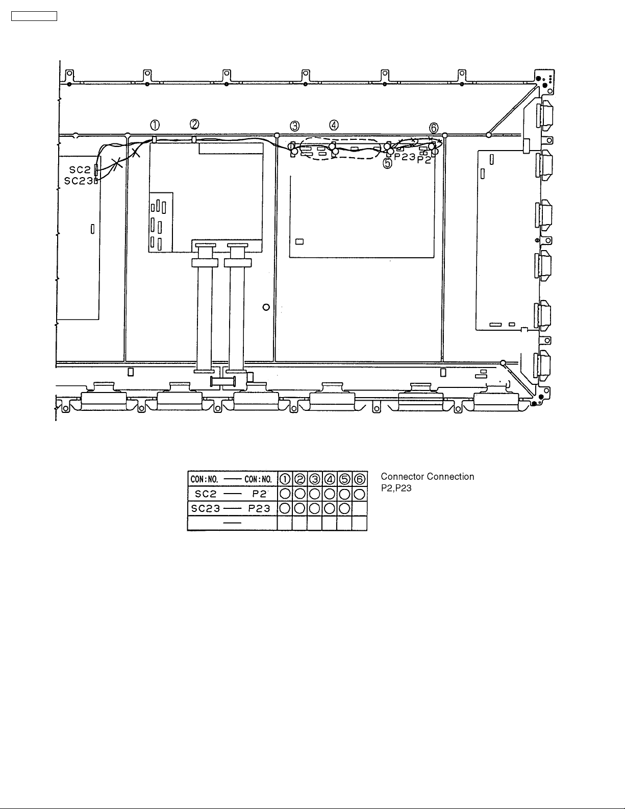
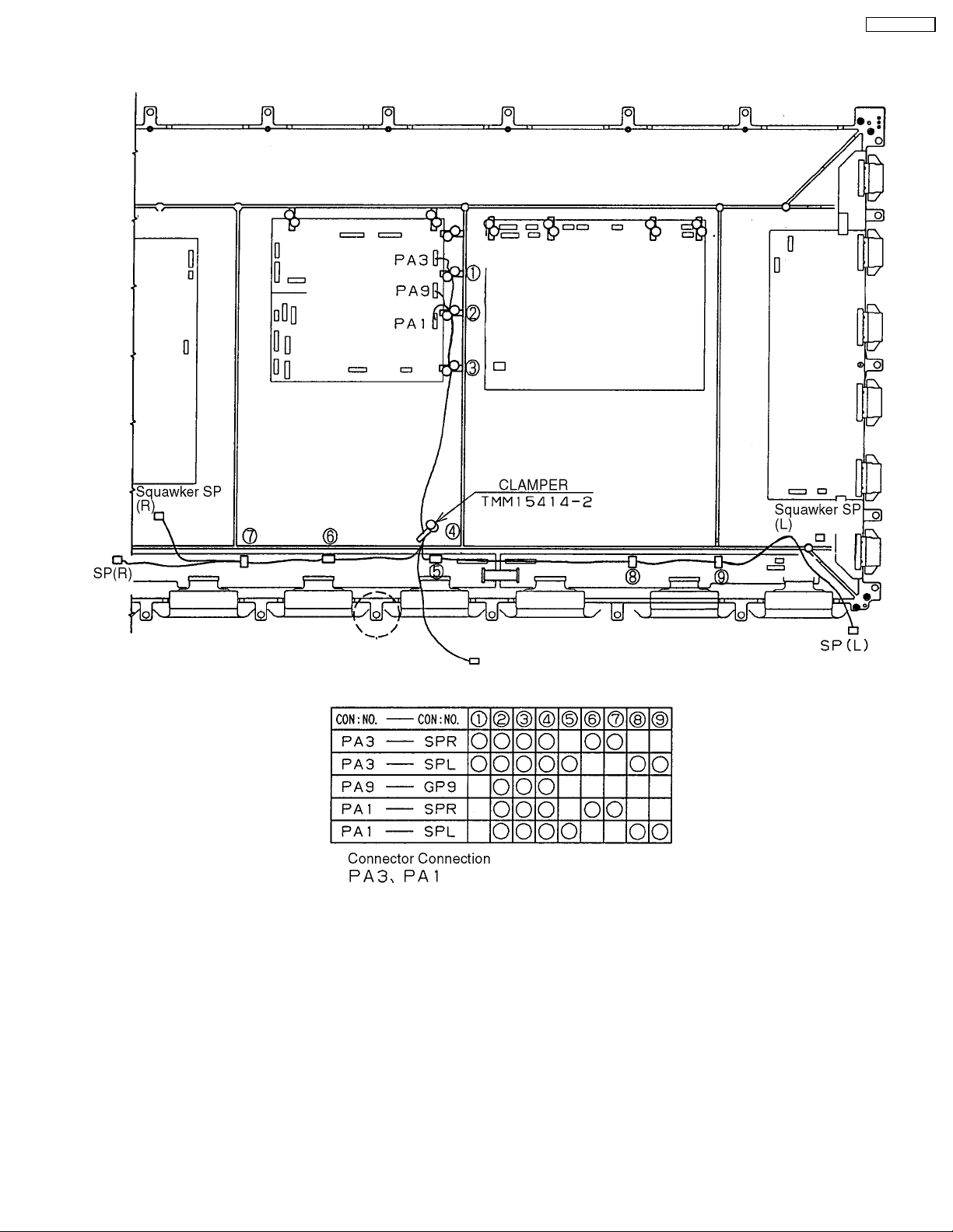
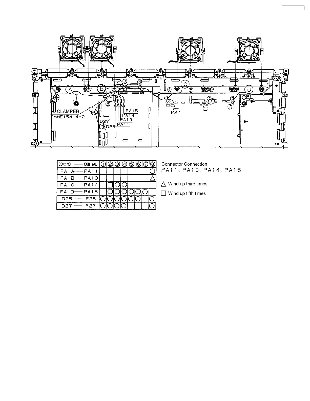
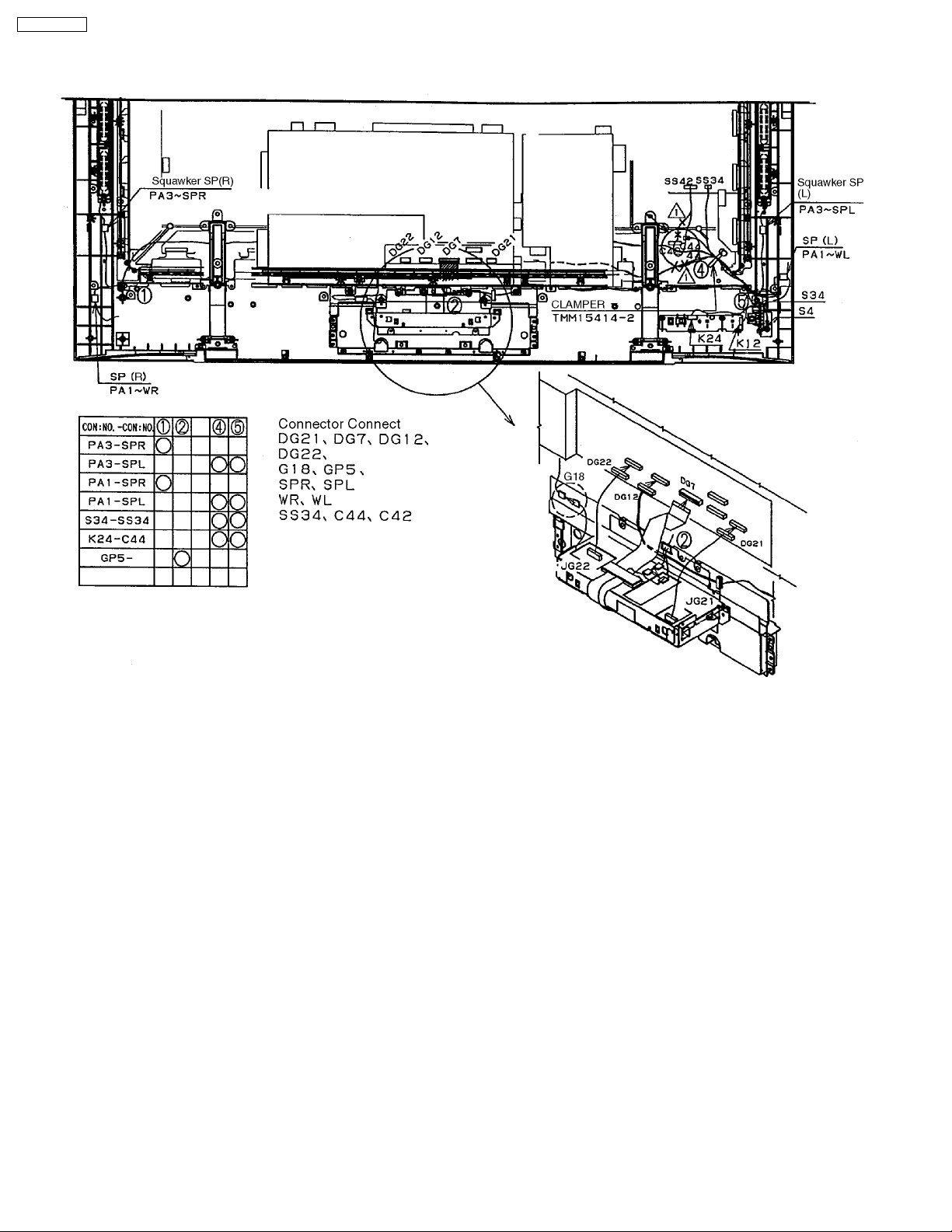
6 Location of Lead Wiring
6.1. Lead of Wiring (1)
TH-42PX20U-P
9
TH-42PX20U-P
6.2. Lead of Wiring (2)
10
6.3. Lead of Wiring (3)
TH-42PX20U-P
11

TH-42PX20U-P
6.4. Lead of Wiring (4)
12
6.5. Lead of Wiring (5)
TH-42PX20U-P
13
TH-42PX20U-P
6.6. Lead of Wiring (6)
14
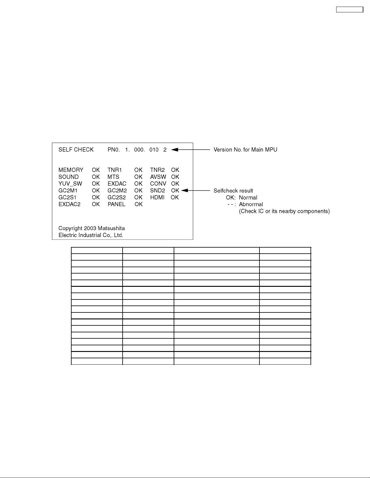
7 Self-check Function
When symptoms like “the power fails sometimes” or “sometimes there is no picture and/or sound” can not be confirmed at the
time of servicing, the self-check function can be used to confirm the occurrence and to find the defective circuit.
In case of “power failure”, flashing of the “POWER” indication (red) at the front of the unit can be used to narrow down the +B
line.
7.1. Self-check of the microcomputer control system (bus line)
Indicaton method
Press the “ACTION” button in the control panel of the unit simultaneously with the “POWER” button in the control panel of the
unit. Hold them few seconds.
Return to he normal screen
Press any button on the unit or in the remote control.
Screen Display
TH-42PX20U-P
Display Ref. No. Description Board
MEMORY IC002 EEPROM for Main MPU DG
SOUND IC2401 Sound Control H
YUV_SW IC4301 YUV switch H
GC2M1 IC4501 Global Core 2 for main DG
GC2S1 IC4502 Global Core 2 for sub DG
EXDAC2 IC5011 EXDAC DV
TNR1 TNR201 Tuner 1 TA
MTS IC4205 Multiplex sound H
EXDAC IC8031 External I/O DG
GC2M2 IC4501 Global Core 2 for main DG
GC2S2 IC4502 Global Core 2 for sub DG
PANEL ----- Panel ----TNR2 TNR251 Tuner 2 TB
AVSW IC4302 AV switch H
CONV IC3801 Convert Micom DG
SND2 IC4203 BBE H
HDMI IC5003 HDMI Recelver DV
15
TH-42PX20U-P
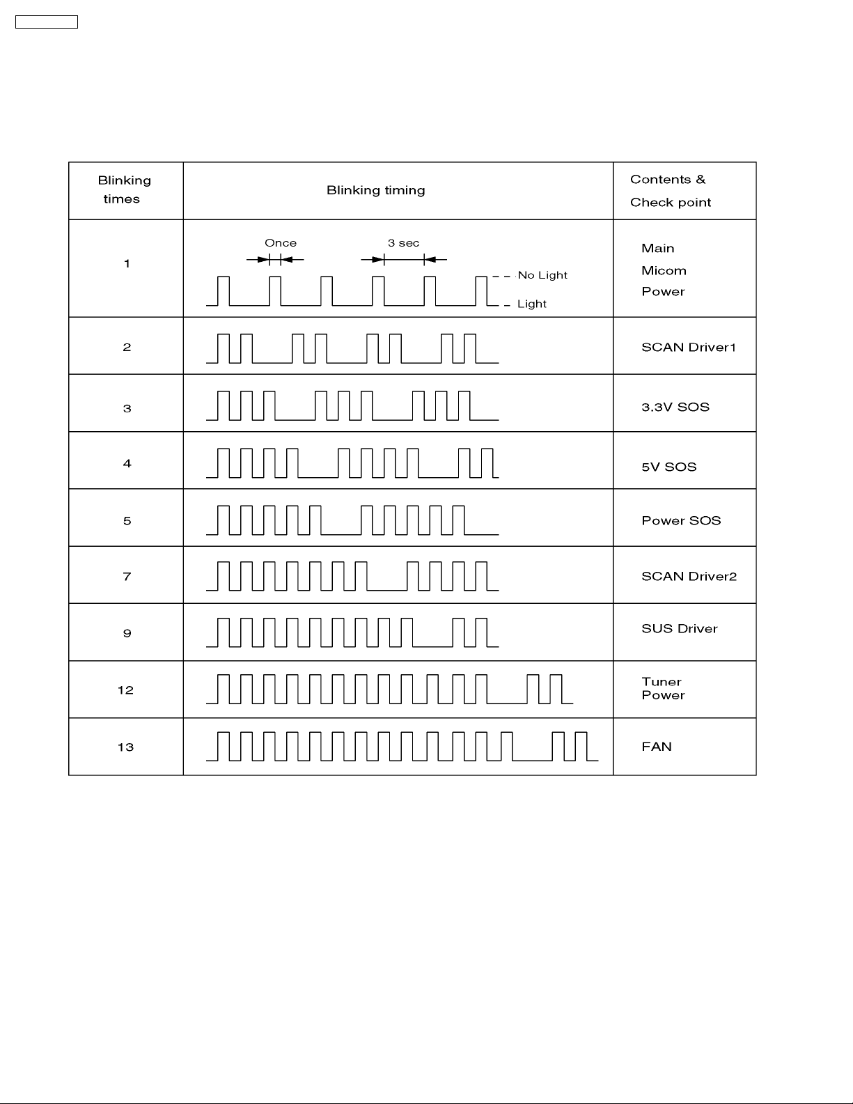
7.2. Power LED Blinking timing chart
1.Subject
Information of LED Flashing timing chart.
2.Contents
When an abnormality has occurred the unit, the protection circuit operates and reset to the stand by mode. At this time, the
defective block can be identified by the number of blinkes of the Power LED on the front panel of the unit.
3.Remarks
Above Fan function is operated during the fans are installed.
16
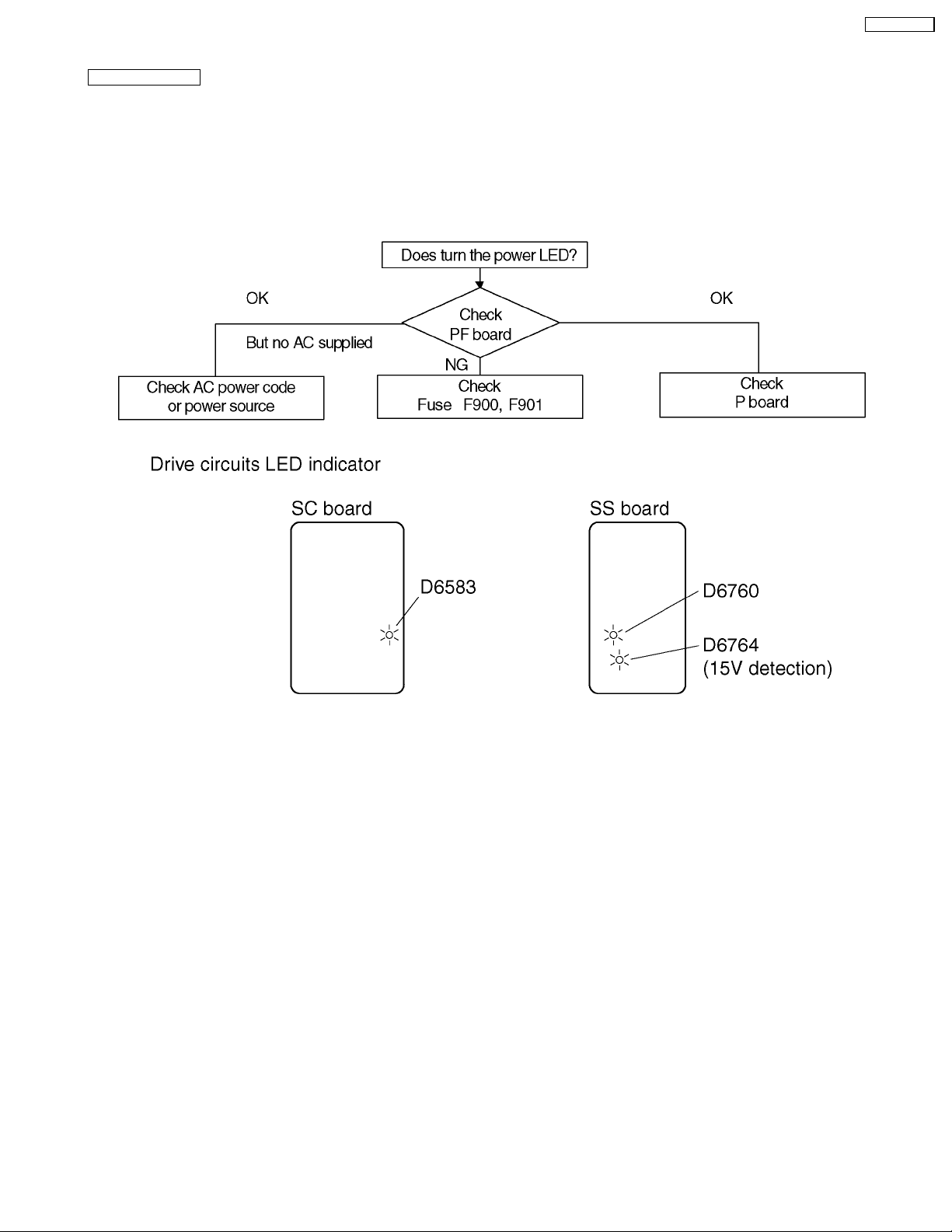
7.3. No Power
First check point
There are following 3 states of No Power indication by power LED.
1.No lit
2.Green is lit then turns red blinking a few seconds later.
3.Only red is lit.
1.No lit
TH-42PX20U-P
17
TH-42PX20U-P
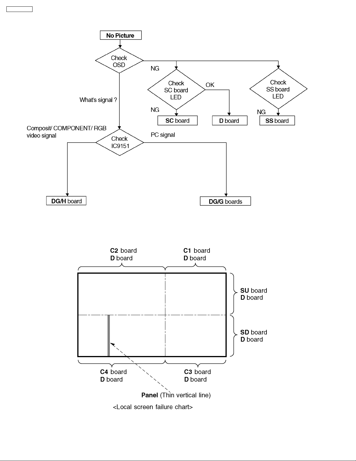
7.4. No Picture
7.5. Local screen failure
Plasma display may have local area failure on the screen. Fig - 1 is the possible defect P.C.B. for each local area.
Fig - 1
18
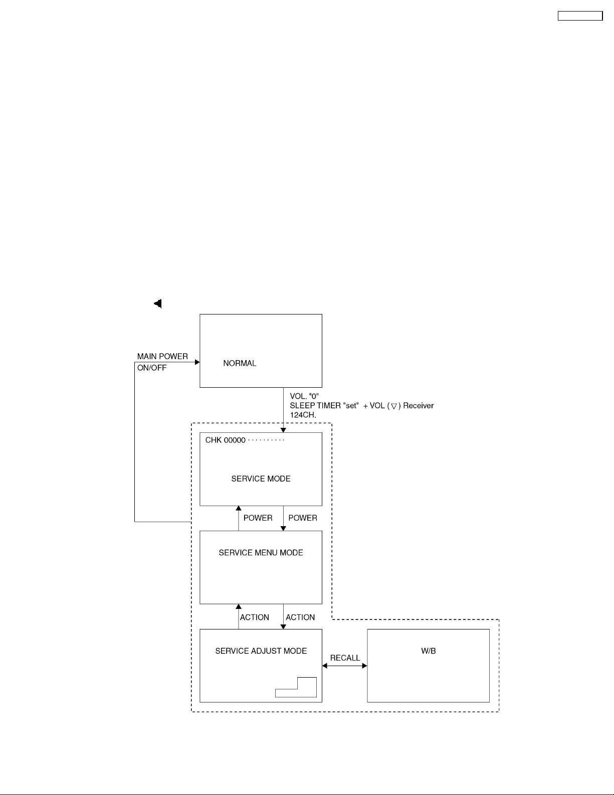
8 Serviceman Mode (Electronic Controls)
This Receiver has electronic technology using the I2C BUS Concept. It performs as a control function and it replaces many
mechanical controls. Instead of adjusting mechanical controls individually, many of the control function are now performed by
using “On Screen Display Menu”. (The Serviceman Adjustment Mode.)
Note
It is suggested that the technician reads all the way through and understand the following the procedure for Entering/Exiting the
Serviceman Mode; then proceed with the instructions working the Receiver. When becoming familiar with the procedure, the
Flow Chart for Serviceman Mode may be used as a quick guide.
Quick Entry to Serviceman Mode:
At times when minor adjustments need to be done to the electronic controls, the method of Entering the serviceman Mode
without removal of the cabinet back is as follows using the Remote Control:
1.Select SET-UP icon and select CABLE mode.
2.Select TIMER icon and set SLEEP time for 30 Min.
3.Press ACTION button twice to exit menus.
4.Tune to the Channel 124.
5.Adjust VOLUME to minimum (0).
6.Press the VOL
button (decrease) on Receiver. Red “CHK” appears in upper corner.
TH-42PX20U-P
7.Press the Power Button on the Remote Control to select one of six Serviceman Adjustment Modes.
a.Serviceman H ADJUSTMENT.
b.Serviceman V ADJUSTM ENT.
19
TH-42PX20U-P
c.Serviceman OTHER ADJUSTMENT.
Exiting the Serviceman Mode:
Press the Power buttons on the Receiver.
For Adjustments:
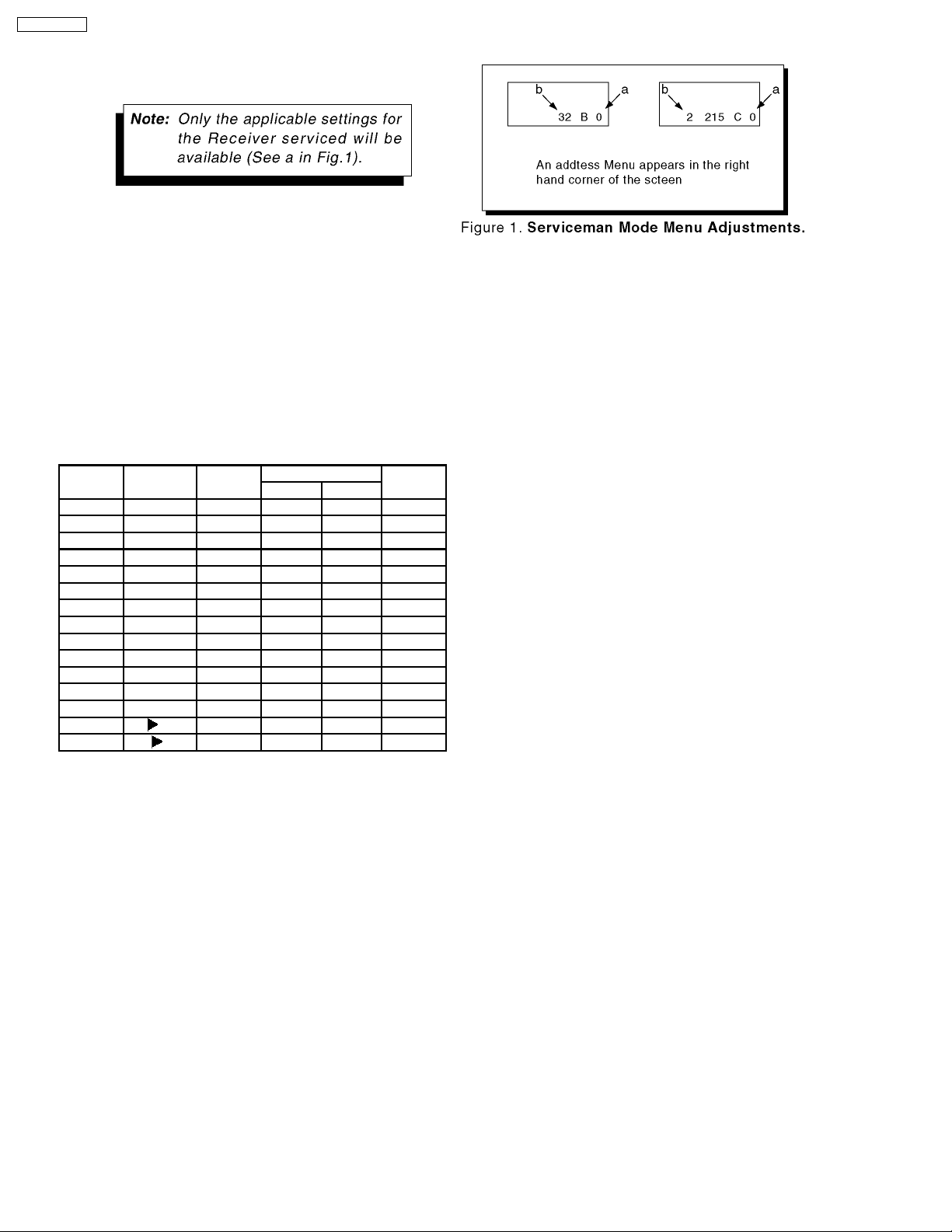
1.Press Channel Up/Down on the Remote Control to select one of the available Service Adjustments (a in Fig.1).
Note:
Write Down the original value set (b in Fig.1) for each address before modifying anything. It is easy to erroneously adjust
the wrong item.
2.Press Volume Up/Down on the Remote Control to adjust the level of the selected Service Adjustment (b in Fig.1).
MAIN
ITEM
H HPOS 15 1C CE
V VPOS 15 1E 0C
OTHER SOSSW 01 97 01
EEP AREA 15 9C ALL
SUB ITEM ORIGINAL
VALUE
HWID 15 1B 2B
HP OF 15 61 FC
HW OF 15 60 00
VWID 15 D1
VP OF 15 20
VW OF 15 29
POFWT 15 89 0A
PSRVS
SPDYN 15 86 -00
IN EX 15 9D
EX IN 15 9E
EEPROM ADRESS DEFAULT
SLEEVE SUB
LEVEL
20
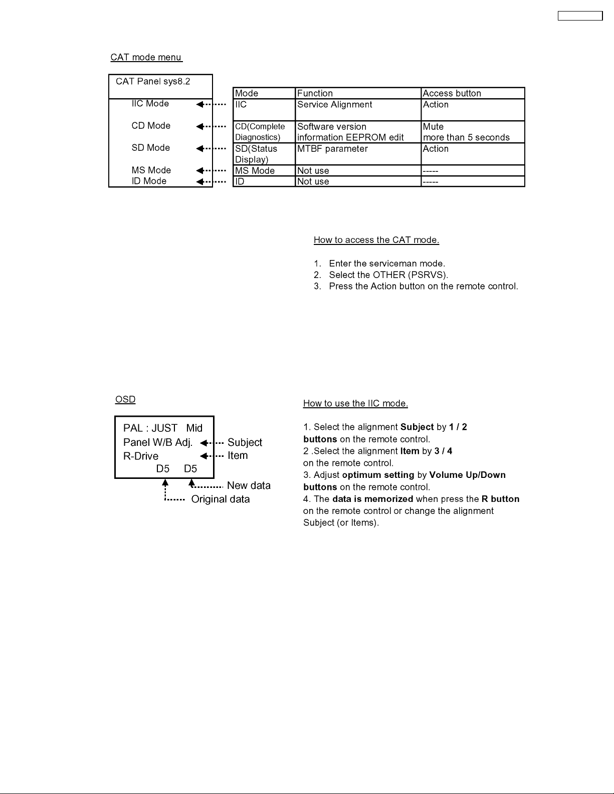
9 CAT (computer Aided Test) mode
TH-42PX20U-P
To exit the CAT mode, access the ID mode and switch off the main power.
9.1. IIC mode
Select the IIC mode by Up/Down button on the remote control at the front page of CAT mode then press the Action button on
the remote control.
“IIC mode structure”.
To exit the IIC mode, press the RECALL button on the remote control.
21
TH-42PX20U-P
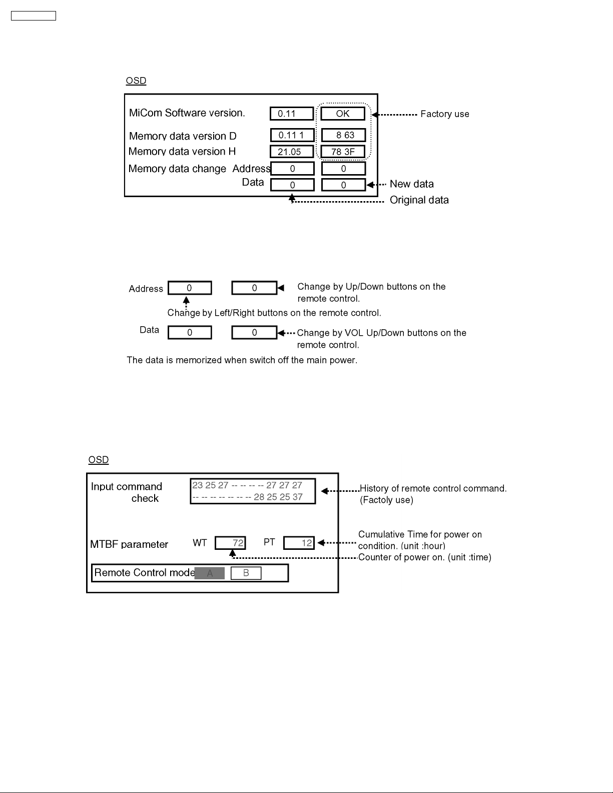
9.2. CD mode
Select the CD mode by Up/Down button on the remote control at the front page of CAT mode then press the Mute button on the
remote control more than 5 sec.
Micom software version (IC9705), this version can be upgrade by
1.replace of new version IC
2.Loading the new version software from loader tool, TZSC07036.
Memory data change
To exit the CD mode, press the RECALL button on the remote control.
9.3. SD mode
Select the SD mode by Up/Down button on the remote control at the front page of CAT mode then press the Action button on the
remote control.
To exit the SD mode, press the RECALL button on the remote control.
22
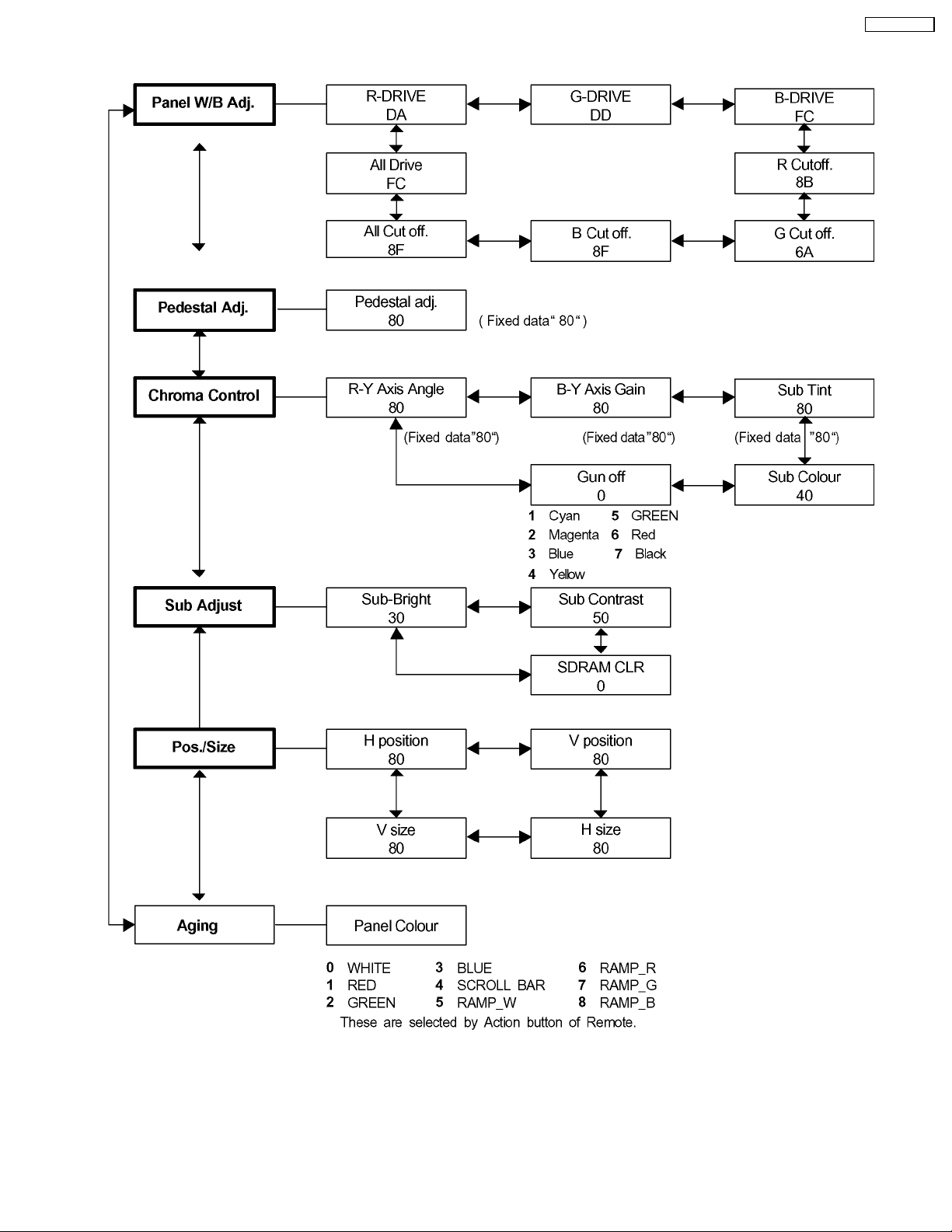
9.4. IIC mode structure (following items value is sample data.)
TH-42PX20U-P
23

TH-42PX20U-P
10 Adjustment Procedure
10.1. Driver Set-up
10.1.1. Item / Preparation
1.Input an APL 100 % white signal.
2.Set the picture controls: Picture mode: Normal
White balance: Cool
Aspect: 16:9
10.1.2. Adjustments
Adjust driver section voltages referring the panel data on the
panel data label.
Name Test Point Voltage Volume Remarks
Vsus TPVSUS
(SS)
Ve TPVE (SS) 150V ± 1V R6770 (SS)
Vset TPVSET
(SC)
Vad TPVAD (SC) -90V ± 1V R6477 (SC)
Vscn TPVSCN
(SC)
Vda TPVDA (SS) 67V ± 1V VR665 (P)
170V ± 2V VR641 (P)
220V ± 5V ---
Vad*+118V ±2V---
*See the Panel label.
24
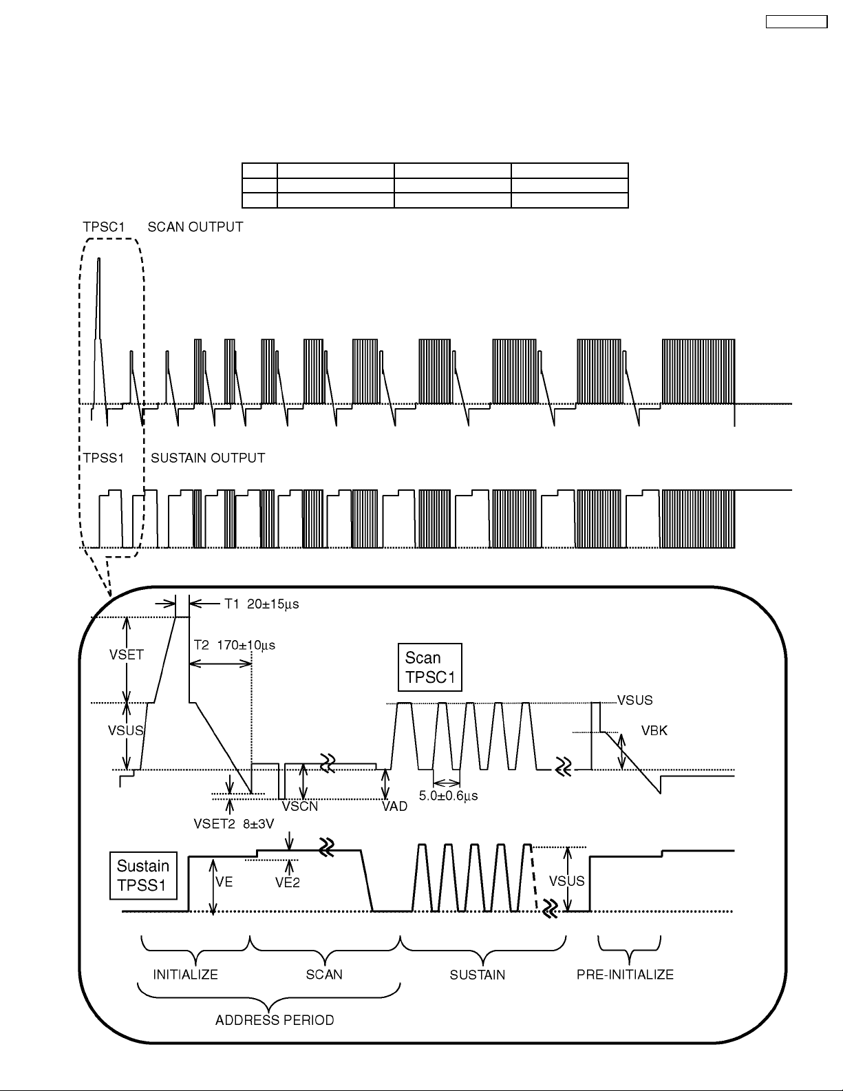
10.2. Initialization Pulse Adjust
1.Input a Cross hatch signal.
2.Set the picture controls: Picture mode: Normal
White balance: Cool
Adjust the indicated test point for the specified wave form.
Test point Volume Level
T1 TPSC1 (SC) --- 20 ± 15µ Sec
T2 TPSS1 (SS) R6557 (SC) 170 ± 10µ Sec
TH-42PX20U-P
25
TH-42PX20U-P
10.3. P.C.B. (Printed Circuit Board) exchange
10.3.1. Caution
1.To remove P.C.B. , wait 1 minute after power was off for discharge from electrolysis capacitors.
10.3.2. Quick adjustment after P.C.B. exchange
P.C.B. Name Test Point Voltage Volume Remarks
P Board Vsus TPVSUS (SS) 170V ± 1V VR641 (P)
Vda TPVDA (SS) 67V ± 1V VR665 (P)
SC Board Vad TPVAD (SC) -90V ± 1V R6477 (SC)
Vset TPVSET (SC) 220V ± 6V ---
Vscn TPVSCN (SC) Vad + 118 ± 2V --SS Board Ve TPVE (SS) 150V ± 1V R6770 (SS)
D, DG Board White blance, Pedestal and Sub brightness for NTSC, PAL, HD, PC and 625i signals
*See the Panel label.
10.4. Adjustment Volume Location
10.5. Test Point Location
26
11 Adjustment
11.1. Pedestal setting
INPUT Alignment menu ProcedureEquipment Setting
1 RF Picture: PANEL W/B
Gray Scale
Pattern
Black 2 %
Black 0 %
White balance: G cut off
Aspect:
Normal R cut off 1) Set R,G and B cut off to "
Cool B cut off
Chroma Control:
16:9
RGB Sub Adjust:
Chroma Control:
RGB Sub Adjust:
Chroma Control:
RGB Sub Adjust:
Gun off
G Sub Bright
Gun off
B Sub Bright
Gun off
R Sub Bright
** Adjust at the dark room.
80 ".
2) Set Gun off to "
3) Adjust G Sub bright 1 to start some of green pixels emission
at black 2% area and no emission at black 0% area.
4) Set Gun off to "
5) Adjust B Sub bright 1 to start some of blue pixels emission
at black 2% area and no emission at black 0% area.
6) Set Gun off to "
7) Adjust R Sub bright 1 to start some of red pixels emission
at black 2% area and no emission at black 0% area.
5". (Only green pixels can emit.)
3". (Only blue pixels can emit.)
6". (Only red pixels can emit.)
TH-42PX20U-P
2 HD Picture: 1) Change input to HD signal.
Gray Scale Normal PANEL W/B
Pattern White balance: R,G,B cut off 2) Repeat procedure 1) to 7) of Component input signal.
Cool PANEL W/B
Aspect: R,G,B Drive
16:9
Black 2 %
Black 0 %
27
TH-42PX20U-P
11.2. NTSC panel white balance
INPUT Alignment menu ProcedureEquipment Setting
1 NTSC Color Picture: 1) Find the nearest area to brightness of 10 cd/m2 as Low
Gray Scale Analyzer Normal Sub Adjust light by color sensor.
Pattern White balance: Sub Bright 2) Adjust Sub bright to set Low light level to 10 cd/m
Aspect: PANEL W/B
High light 75% Sub Adjust
Low light 15% Sub Bright 5) If Sub Bright is changed re-adjust it to set Low light
Cool exactly.
16:9 G cut off 3) Set G cut off to " 80 ".
PANEL W/B
B cut off 4) Adjust B and R cut off to set color temperature as
R cut off shown Fig.-01.
to 10 cd/m
2
.
6)Find 75% of white area by color sensor.
PANEL W/B
G Drive 7) Set G Drive to " E8 ".
PANEL W/B
B Drive 8) Adjust B and R Drive to set color temperature
R Drive as shown Fig.-01.
9) Repeat item 4) to 7) to set both Low light and
high light.
PANEL W/B
R,G,B Drive 10) Increase same steps of R, G and B Drive to set
R,G,B Drive largest level of 3 color drive to "FC".
PANEL W/B
R,G,B cut off 11) Re-adjust Low light level again.
2
Color Temp. x y
Cool 0.276 0.276
Normal 0.288 0.296
Warm 0.313 0.329
Fig. -01
2 Picture: 1) Change white balance to "Normal".
Normal PANEL W/B
White balance: R,G,B cut off 2) Repeat procedure 3) to 11) of Cool mode.
Normal PANEL W/B
Aspect: R,G,B Drive
16:9
3 Picture: 1) Change white balance to "Warm".
Normal PANEL W/B
White balance: R,G,B cut off 2) Repeat procedure 3) to 11) of Cool mode.
Warm PANEL W/B
Aspect: R,G,B Drive
16:9
4 Picture: Picture Menu 1) Change color templature to "Cool".
Normal Sub Adjust
White balance: Sub Bright 2)Re-set Sub bright to "30"
Cool
Aspect:
16:9
28

11.3. HD panel white balance
INPUT Alignment menu ProcedureEquipment Setting
HD
1
Gray Scale
Pattern
High light 75%
Low light 15%
Color Picture: 1) Find the nearest area to brightness of 10 cd/m2 as Low
Analyzer Normal Sub Adjust light by color sensor.
White balance: Sub Bright 2) Adjust Sub bright to set Low light level to 10 cd/m
Cool
Aspect: PANEL W/B
16:9 G cut off 3) Set G cut off to " 80 ".
PANEL W/B
Sub Adjust
Sub Bright 5) If Sub Bright is changed re-adjust it to set Low light
PANEL W/B
PANEL W/B
exactly.
B cut off 4) Adjust B and R cut off to set color temperature as
R cut off shown Fig.-04.
to 10 cd/m
2
.
6)Find 75% of white area by color sensor.
G Drive 7) Set G Drive to " E8 ".
B Drive 8) Adjust B and R Drive to set color temperature
R Drive as shown Fig.-04.
TH-42PX20U-P
2
9) Repeat item 4) to 7) to set both Low light and
high light.
PANEL W/B
R,G,B Drive 10) Increase same steps of R, G and B Drive to set
R,G,B Drive largest level of 3 color drive to "FC".
PANEL W/B
R,G,B cut off 11) Re-adjust Low light level again.
Color Temp. x y
Cool 0.276 0.276
Normal 0.288 0.296
Warm 0.313 0.329
Fig. -04
2 Picture: 1) Change white balance to "Normal".
Normal PANEL W/B
White balance: R,G,B cut off 2) Repeat procedure 3) to 11) of Cool mode.
Normal
PANEL W/B
Aspect: R,G,B Drive
16:9
3 Picture: 1) Change white balance to "Warm".
Normal PANEL W/B
White balance: R,G,B cut off 2) Repeat procedure 3) to 11) of Cool mode.
Warm
PANEL W/B
Aspect: R,G,B Drive
16:9
4 Picture: Picture Menu 1) Change color templature to "Cool".
Normal Sub Adjust
White balance: Sub Bright 2)Re-set Sub bright to "30"
Cool
Aspect:
16:9
29
TH-42PX20U-P
11.4. Sub brightness setting
INPUT Alignment menu ProcedureEquipment Setting
1 RF Picture: PANEL W/B
Gray Scale Normal All cut off 1) Set white balance to
Pattern Aspect:
** Adjust at the dark room.
Cool
.
16:9 2) Adjust All cut off to start some pixels emission
at black 2% area and no emission at black 0% area.
3) Write down all cut off data.
4) Set white balance to
Black 2 %
Black 0 % 5) Adjust All cut off to set same data of Cool mode.
6) Set white balance to
7) Adjust All cut off to set same data of Cool mode.
HD 8) Change to HD signal.
Gray Scale
Pattern 9) Copy PAL All cut off data to HD mode.
Nornal
warm
.
.
30
 Loading...