

Panasonic TH-37PV60E, TH-37PX60B, TH-42PV60E, TH-42PX60B Service manual
GP9DE Chassis
A
A
ORDER NO.PCZ0602005CE
Plasma Television
Specifications
Power Source
Power Consumption
Average use 241 W (TH-37PV60E), 250 W (TH-37PX60B)
Standby condition 0.3 W (PV60E)
Plasma Display panel
Drive method
Aspect Ratio 16:9
Contrast Ratio 3000:1
Visible screen size
(No. of pixels)
Sound
Speaker 12 cm × 6 cm × 2 pcs, 8 W
Audio Output 20 W (10 W + 10 W ), 10% THD
Headphones M3 (3.5 mm) Jack × 1
PC signals VGA, SVGA, XGA
Receiving Systems /
Band name (PV60E)
C 220-240 V, 50 / 60 Hz
261 W (TH-42PV60E), 270 W (TH-42PX60B)
0.3 W (PX60B Withou t DVB recording), 20 W (PX60B With DVB recording)
C type
94 cmV (37-inch), 106 cmV (42-inch)
818 mm (W) × 461 mm (H) × 939 mm (diagonal) (37-inch)
920 mm (W) × 518 mm (H) × 1,056 mm (diagonal) (42-inch)
737,280 (1,024 (W) × 720 (H)) [3,072 × 720 dots] (37-inch)
786,432 (1,024 (W) × 768 (H)) [3,072 × 768 dots] (42-inch)
SXGA (compressed)
Horizontal scanning frequency 31 - 69 kHz
Vertical scanning frequency 59 - 86 Hz
PAL B, G, H, I, SECAM B, G SECAM L / L’
VHF E2 - E12 VHF H1 - H2 (ITALY)
VHF A - H (ITALY) UHF E21 - E69
CATV (S01 - S05) CATV S1 - S10 (M1 - M10)
© 2006 Matsushita Electric Industrial Co., Ltd. All
rights reserved. Unauthorized copying and
distribution is a violation of law.

V
TH-37PV60E / TH-37PX60B / TH-42PV60E / TH-42PX60B
CATV S11 - S20 (U1 - U10) CATV S21 - S41 (Hyperband)
PAL D, K, SECAM D, K
VHF R1 - R2
VHF R6 - R12 UHF E21 - E69
PAL 525/60
Playback of NTSC tape from some PAL Video recorders (VCR)
M.NTSC
Playback from M. NTSC Video recorders (VCR)
NTSC (AV input only)
Playback from NTSC Video recorders (VCR)
Receiving Systems /
Band name (PX60B)
PAL I
UHF E21 - 68.
PAL 525/60
Playback of NTSC tape from some PAL Video recorders (VCR) or NTSC disc playback from DVD
player and recorder.
DVB
Digital terrestrial services via UHF aerial input.
M.NTSC
Playback from M.NTSC Video recorders (VCR).
NTSC (AV input only)
Playback from NTSC Video recorders (VCR).
Aerial - Rear VHF / UHF (PV60E)
UHF (PX60B)
Operating Conditions Temperature : 0°C-40°C
Humidity : 20 % - 80 % RH (non-condensing)
Connection Terminals
AV1 (Scart terminal) 21 Pin terminal (Audio / Video in, Audio / Video out, RGB in)
AV2 (Scart terminal) 21 Pin terminal (Audio / Video in, Audio / Video out, S-Video in, Q-Link)
AV3 (Scart terminal) 21 Pin terminal (Audio / Video in, Audio / Video out, RGB in, S-Video in, Q-Link)
AV4 VIDEO RCA PIN Type × 1 1.0 V[p-p] (75 W)
S-VIDEO Mini DIN 4-pin Y:1.0 V[p-p] (75 W) C:0.286 V[p-p] (75 W)
AUDIO L - R RCA PIN Type × 2 0.5 V[rms]
Others COMPONENT Y
P
B,PR
HDMI 1/2 TYPE A Connectors
PC HIGH-DENSITY D-SUB 15PIN R,G,B/0.7 V[p-p] (75 W)
AUDIO L - R RCA PIN Type × 2 0.5 V[rms]
Output AUDIO L - R RCA PIN Type × 2 0.5 V[rms] (high impedance)
Dimensions ( W × H × D )
917 mm × 645 mm × 95 mm (37-inch)
1,020 mm × 705 mm × 95 mm (42-inch)
Weight
26.0 kg Net (37-inch)
30.0 kg Net (42-inch)
HF R3 - R5
1.0 V[p-p] (including synchronization)
±0.35 V[p-p]
HD, VD/TTL Level 2.0 - 5.0 V[p-p] (high impedance)
Notes:
· Design and Specifications are subject to change without notice. Weight and Dimensions shown are approximate.
· This equipment complies with the EMC standards listed below.
EN55013, EN61000-3-2, EN61000-3-3, EN55020, EN55022, EN55024.
2
TH-37PV60E / TH-37PX60B / TH-42PV60E / TH-42PX60B
CONTENTS
Page Page
1 Applicable signals 5
2 Safety Precautions
2.1. General Guidelines
2.2. Touch-Current Check
3 Prevention of Electro Static Discharge (ESD) to
Electrostatically Sensitive (ES) Devices
4 About lead free solder (PbF)
5 Service Hint
6 Plasma panel replacement method
6.1. Remove the Back cover
6.2. Remove the fan
6.3. Remove the rear terminal cover
6.4. Remove the P-Board
6.5. Remove the PA-Board
6.6. Remove the tuner unit
6.7. Remove the XV-Board (PX60B)
6.8. Remove the DG-Board
6.9. Remove the TA-Board
6.10. Remove the H-Board
6.11. Remove the HC-Board
6.12. Remove the D-Board
6.13. Remove the SU-Board (37inch)
6.14. Remove the SU-Board (42inch)
6.15. Remove the SD-Board (37inch)
6.16. Remove the SD-Board (42inch)
6.17. Remove the SC-Board
6.18. Remove the SS-Board
6.19. Remove the C1-Board
6.20. Remove the C2-Board
6.21. Remove the front bracket
6.22. Remove the G-Board and GK-Board
6.23. Remove the speaker L, R
6.24. Remove the S-Board
6.25. Remove the K-Board
6.26. Remove the stand brackets
6.27. Remove the Plasma panel section from the Front frame
(glass)
6.28. Replace the plasma panel (finished)
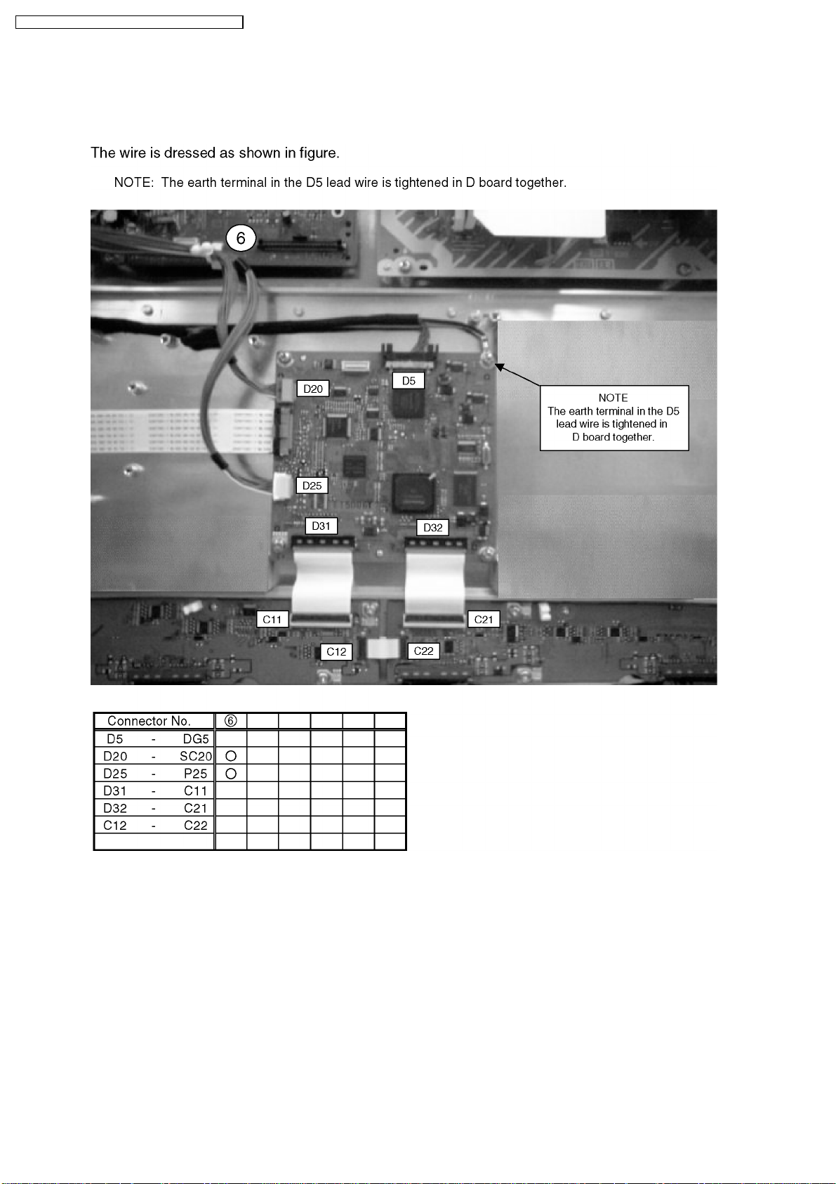
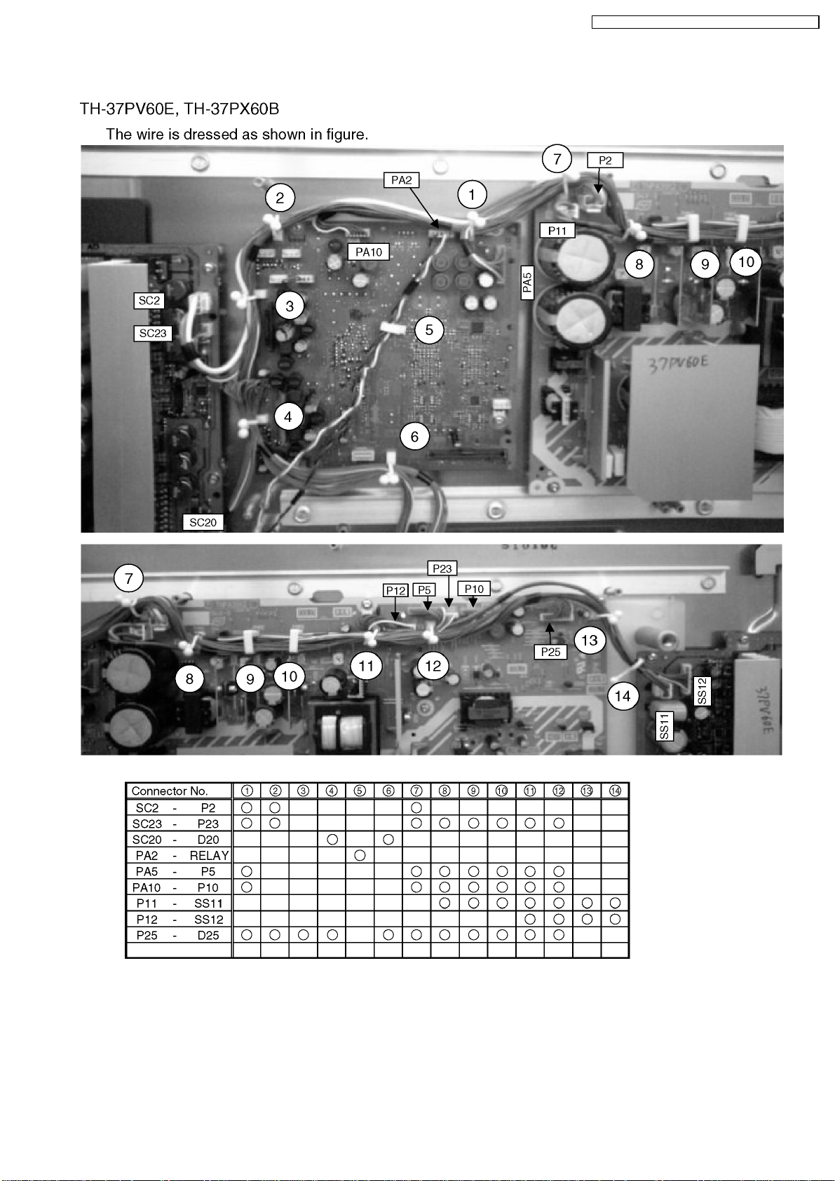
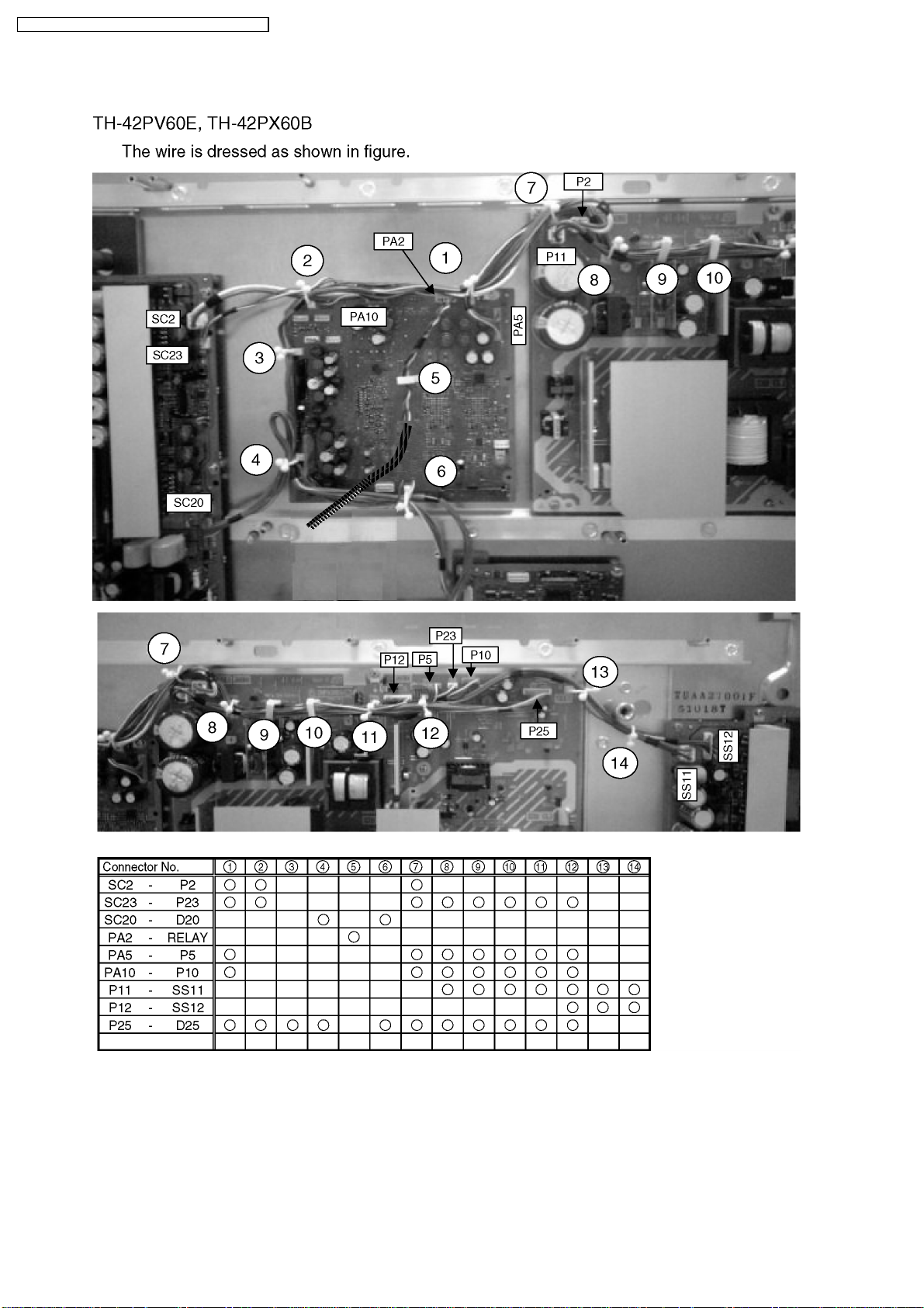
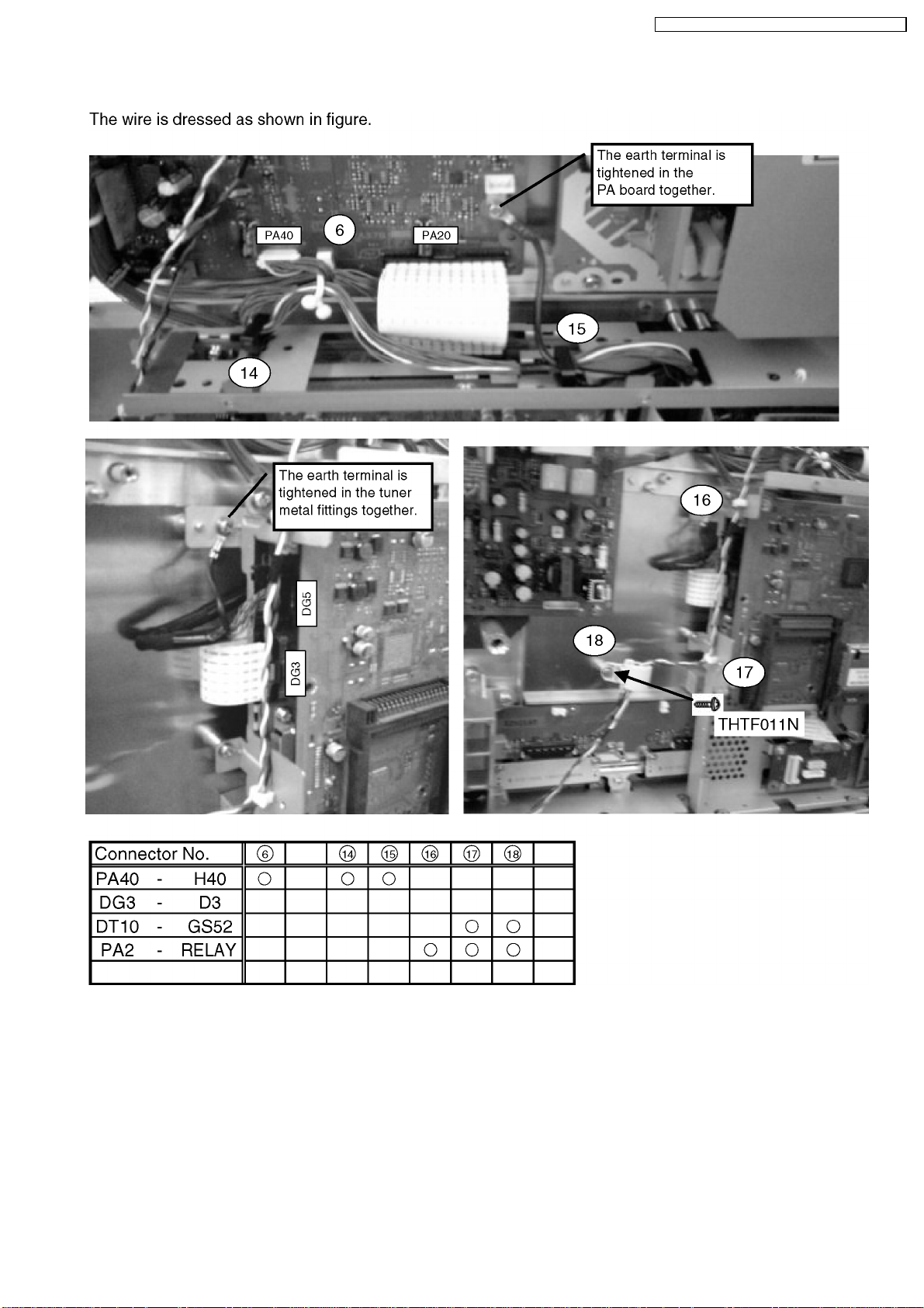
7 Location of Lead Wiring
7.1. Lead of Wiring (1)
7.2. Lead of Wiring (2)
7.3. Lead of Wiring (3)
7.4. Lead of Wiring (4)
7.5. Lead of Wiring (5)
7.6. Lead of Wiring (6)
7.7. Lead of Wiring (7)
10
10
10
10
10
11
11
11
12
12
12
13
13
13
13
14
14
14
14
15
15
15
16
16
16
17
17
17
17
18
18
19
20
21
22
23
24
6
6
6
7
8
9
7.8. Lead of Wiring (8)
8 Self Check
8.1. Power LED Blinking timing chart
8.2. No Power
8.3. No Picture
8.4. Local screen failure
9 Service Mode Function
9.1. How to enter SERVICE 1
9.2. How to enter SERVICE 2
9.3. Option Description
10 Adjustment Procedure
10.1. Driver Set-up
10.2. Initialization Pulse Adjust
10.3. P.C.B. (Printed Circuit Board) exchange
10.4. Adjustment Volume Location
10.5. Test Point Location
11 Adjustment
11.1. PAL panel white balance adjustment
11.2. HD white balance adjustment
11.3. Sub bright adjustment
11.4. ABL adjustment
12 Hotel mode
13 Concuct Views
13.1. P-Board (37inch)
13.2. P-Board (42inch)
13.3. PA-Board
13.4. H-Board
13.5. G and TA-Board
13.6. GK, HC, K and S-Board
13.7. DG-Board
13.8. XV-Board (PX60B)
13.9. D-Board
13.10. C1-Board (37inch)
13.11. C1-Board (42inch)
13.12. C2-Board (37inch)
13.13. C2-Board (42inch)
13.14. SC-Board
13.15. SU-Board (37inch)
13.16. SU-Board (42inch)
13.17. SD-Board (37inch)
13.18. SD-Board (42inch)
13.19. SS-Board
14 Sche maatic and Block Diagr am
14.1. Schematic Diagram Notes
14.2. Main Block Diagram (37inch)
14.3. Main Block Diagram (42inch)
25
26
27
28
29
30
31
31
31
33
35
35
36
36
37
37
38
38
39
40
41
42
43
43
46
49
51
53
54
55
57
59
61
62
63
64
65
68
69
70
71
72
75
75
76
77
3
TH-37PV60E / TH-37PX60B / TH-42PV60E / TH-42PX60B
14.4. P-Board Block Diagram (37inch) 78
14.5. P-Board (1 of 6) Schematic Diagram (37inch)
14.6. P-Board (2 of 6) Schematic Diagram (37inch)
14.7. P-Board (3 of 6) Schematic Diagram (37inch)
14.8. P-Board (4 of 6) Schematic Diagram (37inch)
14.9. P-Board (5 of 6) Schematic Diagram (37inch)
14.10. P-Board (6 of 6) Schematic Diagram (37inch)
14.11. P-Board Block Diagram (42inch)
14.12. P-Board (1 of 6) Schematic Diagram (42inch)
14.13. P-Board (2 of 6) Schematic Diagram (42inch)
14.14. P-Board (3 of 6) Schematic Diagram (42inch)
14.15. P-Board (4 of 6) Schematic Diagram (42inch)
14.16. P-Board (5 of 6) Schematic Diagram (42inch)
14.17. P-Board (6 of 6) Schematic Diagram (42inch)
14.18. PA-Board Block Diagram
14.19. PA-Board (1 of 3) Schematic Diagram
14.20. PA-Board (2 of 3) Schematic Diagram
14.21. PA-Board (3 of 3) Schematic Diagram
14.22. H and TA-Board Block Diagram
14.23. G, GK, HC and K-Board Block Diagram
14.24. H-Board (1 of 3)Schematic Diagram
14.25. H-Board (2 of 3)Schematic Diagram
14.26. H-Board (3 of 3)Schematic Diagram
14.27. G-Board Schematic Diagram
14.28. GK, K, HC and TA-Board Schematic Diagram
14.29. DG-Board (1 of 3) Block Diagram
14.30. DG-Board (2 of 3) Block Diagram
14.31. DG-Board (3 of 3) Block Diagram
14.32. DG-Board (1 of 8) Schematic Diagram
14.33. DG-Board (2 of 8) Schematic Diagram
14.34. DG-Board (3 of 8) Schematic Diagram
14.35. DG-Board (4 of 8) Schematic Diagram
14.36. DG-Board (5 of 8) Schematic Diagram
14.37. DG-Board (6 of 8) Schematic Diagram
14.38. DG-Board (7 of 8) Schematic Diagram
14.39. DG-Board (8 of 8) Schematic Diagram
14.40. XV-Board Block Diagram (PX60B)
14.41. XV-Board (1 of 5) Schematic Diagram (PX60B)
14.42. XV-Board (2 of 5) Schematic Diagram (PX60B)
14.43. XV-Board (3 of 5) Schematic Diagram (PX60B)
14.44. XV-Board (4 of 5) Schematic Diagram (PX60B)
79
80
81
82
83
84
85
86
87
88
89
90
91
92
93
94
95
96
97
98
99
100
101
102
103
104
105
106
107
108
109
110
111
112
113
114
115
116
117
118
14.45. XV-Board (5 of 5) Schematic Diagram (PX60B)
14.46. D-Board Block Diagram
14.47. D-Board (1 of 6) Schematic Diagram
14.48. D-Board (2 of 6) Schematic Diagram
14.49. D-Board (3 of 6) Schematic Diagram
14.50. D-Board (4 of 6) Schematic Diagram
14.51. D-Board (5 of 6) Schematic Diagram
14.52. D-Board (6 of 6) Schematic Diagram
14.53. C1 and C2-Board Block Diagram
14.54. C1-Board (1 of 2) Schematic Diagram (37inch)
14.55. C1-Board (2 of 2) Schematic Diagram (37inch)
14.56. C1-Board (1 of 2) Schematic Diagram (42inch)
14.57. C1-Board (2 of 2) Schematic Diagram (42inch)
14.58. C2-Board (1 of 2) Schematic Diagram (37inch)
14.59. C2-Board (2 of 2) Schematic Diagram (37inch)
14.60. C2-Board (1 of 2) Schematic Diagram (42inch)
14.61. C2-Board (2 of 2) Schematic Diagram (42inch)
14.62. SC, SU and SD-Board Block Diagram (37inch)
14.63. SC, SU and SD-Board Block Diagram (42inch)
14.64. SC-Board (1 of 2) Schematic Diagram
14.65. SC-Board (2 of 2) Schematic Diagram
14.66. SU-Board (1 of 2) Schematic Diagram (37inch)
14.67. SU-Board (2 of 2) Schematic Diagram (37inch)
14.68. SU-Board (1 of 2) Schematic Diagram (42inch)
14.69. SU-Board (2 of 2) Schematic Diagram (42inch)
14.70. SD-Board (1 of 2) Schematic Diagram (37inch)
14.71. SD-Board (2 of 2) Schematic Diagram (37inch)
14.72. SD-Board (1 of 2) Schematic Diagram (42inch)
14.73. SD-Board (2 of 2) Schematic Diagram (42inch)
14.74. SS and S-Board Block Diagram
14.75. SS and S-Board Schematic Diagram
15 Parts Locat ion & Mechanica l Replaceme n t Parts List
15.1. Parts Location
15.2. Packing Exploded Views (1)
15.3. Packing Exploded Views (2)
15.4. Packing Exploded Views (3)
15.5. Mechanical Replacement Parts List
16 Elect ri cal Repla cement Parts List
16.1. Replacement Parts List Notes
16.2. Electrical Replacement Parts List (37inch)
16.3. Electrical Replacement Parts List (42inch)
119
120
121
122
123
124
125
126
127
128
129
130
131
132
133
134
135
136
137
138
139
140
141
142
143
144
145
146
147
148
149
151
151
152
153
154
155
157
157
158
188
4
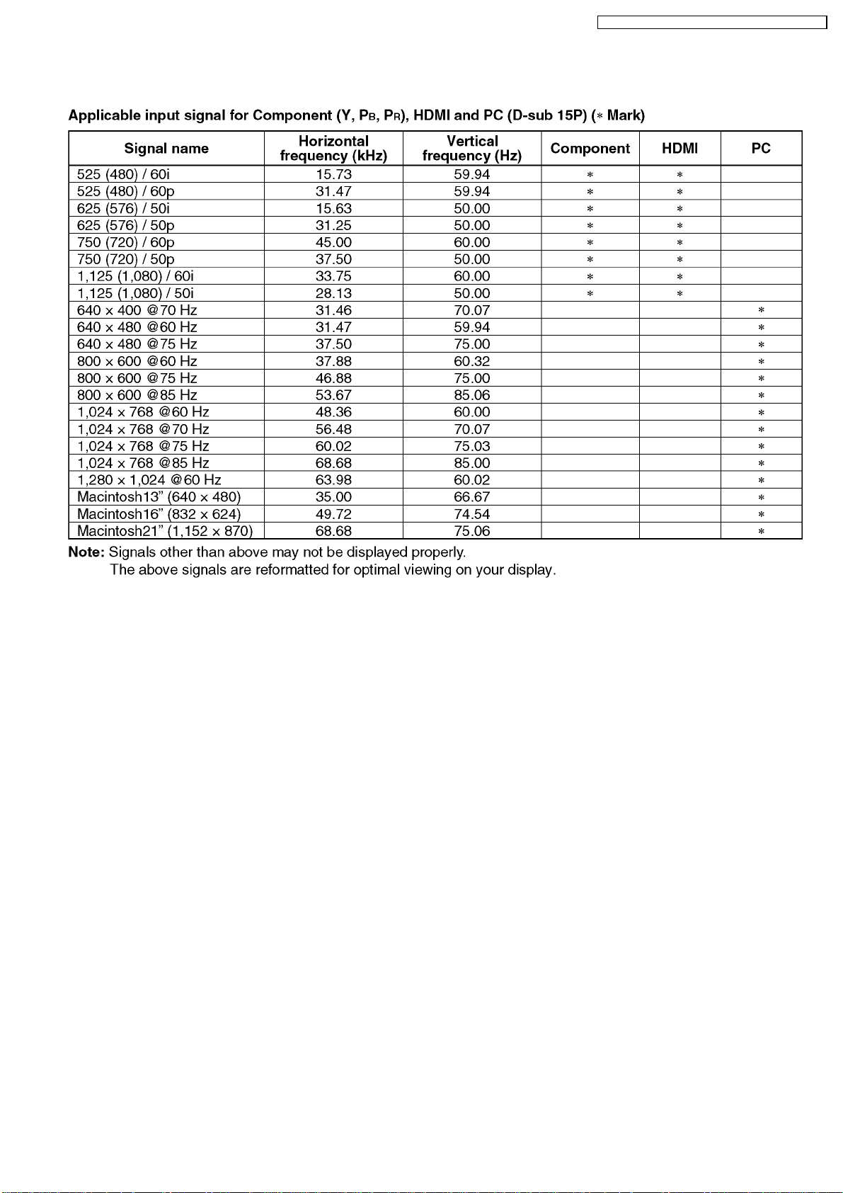
1 Applicable signals
TH-37PV60E / TH-37PX60B / TH-42PV60E / TH-42PX60B
5
TH-37PV60E / TH-37PX60B / TH-42PV60E / TH-42PX60B
2 Safety Precautions
2.1. General Guidelines
1. When servicing, observe the original lead dress. If a short circuit is found, replace all parts which have been overheated or
damaged by the short circuit.
2. After servicing, see to it that all the protective devices such as insulation barriers, insulation papers shields are properly
installed.
3. After servicing, make the following leakage current checks to prevent the customer from being exposed to shock hazards.
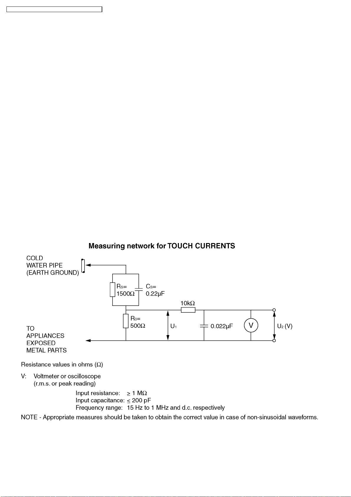
2.2. Touch-Current Check
1. Plug the AC cord directly into the AC outlet. Do not use an isolation transformer for this check.
2. Connect a measuring network for touch currents between each exposed metallic part on the set and a good earth ground such
as a water pipe, as shown in Figure 1.
3. Use Leakage Current Tester (Simpson 228 or equivalent) to measure the potential across the measuring network.
4. Check each exposed metallic part, and measure the voltage at each point.
5. Reserve the AC plug in the AC outlet and repeat each of the above measure.
6. The potential at any point (TOUGH CURRENT) expressed as voltage U
For a. c.: U
For d. c.: U
= 35 V (peak) and U2= 0.35 V (peak);
1
=1.0V,
1
Note:
The limit value of U
= 0.35 V (peak) for a. c. and U1= 1.0 V for d. c. correspond to the values 0.7 mA (peak) a. c. and 2.0
2
mA d. c.
The limit value U
= 35 V (peak) for a. c. correspond to the value 70 mA (peak) a. c. for frequencies greater than 100 kHz.
1
7. In case a measurement is out of the limits specified, there is a possibility of a shock hazard, and the equipment should be
repaired and rechecked before it is returned to the customer.
and U2, does not exceed the following values:
1
Figure 1
6
TH-37PV60E / TH-37PX60B / TH-42PV60E / TH-42PX60B
3 Prevention of Electro Static Discharge (ESD) to
Electrostatically Sensitive (ES) Devices
Some semiconductor (solid state) devices can be damaged easily by static electricity. Such components commonly are called
Electrostatically Sensitive (ES) Devices. Examples of typical ES devices are integrated circuits and some field-effect transistors and
semiconductor "chip" components. The following techniques should be used to help reduce the incidence of component damage
caused by electro static discharge (ESD).
1. Immediately before handling any semiconductor component or semiconductor-equipped assembly, drain off any ESD on your
body by touching a known earth ground. Alternatively, obtain and wear a commercially available discharging ESD wrist strap,
which should be removed for potential shock reasons prior to applying power to the unit under test.
2. After removing an electrical assembly equipped with ES devices, place the assembly on a conductive surface such as alminum
foil, to prevent electrostatic charge buildup or exposure of the assembly.
3. Use only a grounded-tip soldering iron to solder or unsolder ES devices.
4. Use only an anti-static solder removal device. Some solder removal devices not classified as "anti-static (ESD protected)" can
generate electrical charge sufficient to damage ES devices.
5. Do not use freon-propelled chemicals. These can generate electrical charges sufficient to damage ES devices.
6. Do not remove a replacement ES device from its protective package until immediately before you are ready to install it. (Most
replacement ES devices are packaged with leads electrically shorted together by conductive foam, alminum foil or comparable
conductive material).
7. Immediately before removing the protective material from the leads of a replacement ES device, touch the protective material
to the chassis or circuit assembly into which the device will be installed.
Caution
Be sure no power is applied to the chassis or circuit, and observe all other safety precautions.
8. Minimize bodily motions when handling unpackaged replacement ES devices. (Otherwise hamless motion such as the brushing
together of your clothes fabric or the lifting of your foot from a carpeted floor can generate static electricity (ESD) sufficient to
damage an ES device).
7
TH-37PV60E / TH-37PX60B / TH-42PV60E / TH-42PX60B
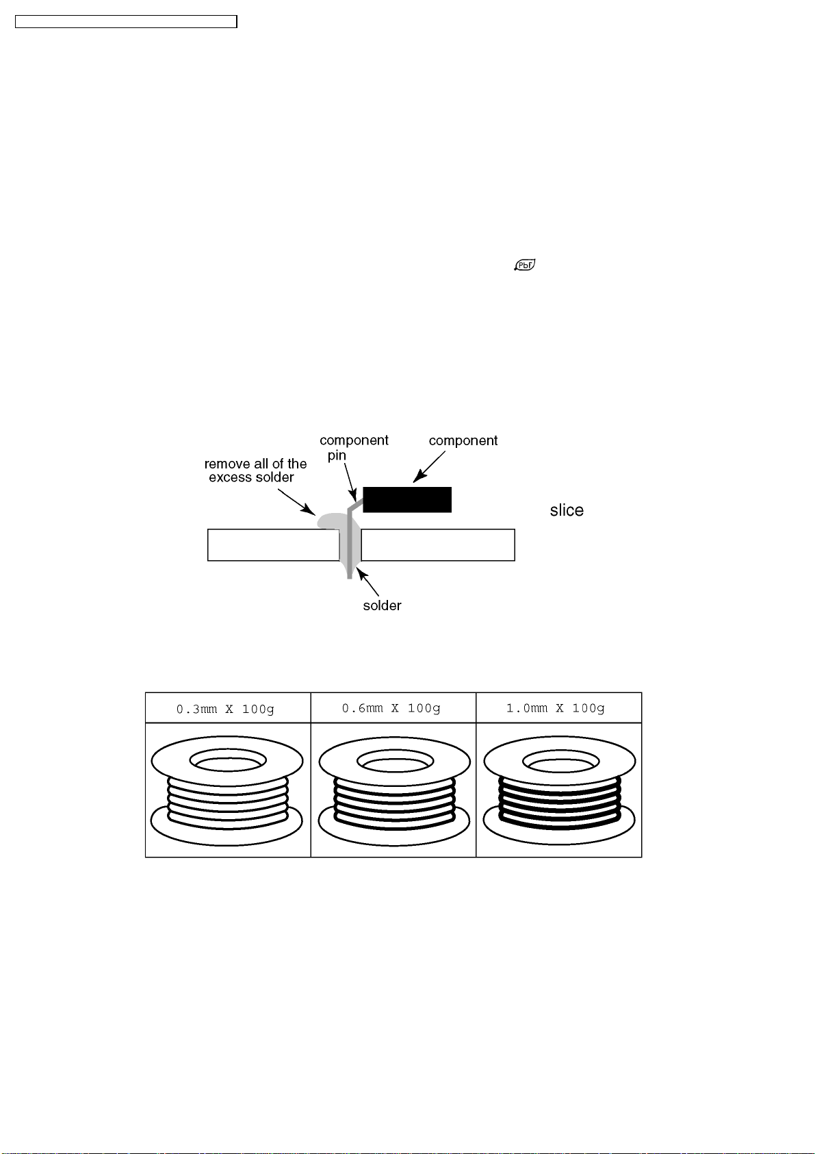
4 About lead free solder (PbF)
Note: Lead is listed as (Pb) in the periodic table of elements.
In the information below, Pb will refer to Lead solder, and PbF will refer to Lead Free Solder.
The Lead Free Solder used in our manufacturing process and discussed below is (Sn+Ag+Cu).
That is Tin (Sn), Silver (Ag) and Copper (Cu) although other types are available.
This model uses Pb Free solder in it’s manufacture due to environmental conservation issues. For service and repair work, we’d
suggest the use of Pb free solder as well, although Pb solder may be used.
PCBs manufactured using lead free solder will have the PbF within a leaf Symbol
Caution
· Pb free solder has a higher melting point than standard solder. Typically the melting point is 50 ~ 70 °F (30~40 °C) higher.
Please use a high temperature soldering iron and set it to 700 ± 20 °F (370 ± 10 °C).
· Pb free solder will tend to splash when heated too high (about 1100 °F or 600 °C).
If you must use Pb solder, please completely remove all of the Pb free solder on the pins or solder area before applying Pb
solder. If this is not practical, be sure to heat the Pb free solder until it melts, before applying Pb solder.
· After applying PbF solder to double layered boards, please check the component side for excess solder which may flow onto
the opposite side. (see figure below)
Suggested Pb free solder
There are several kinds of Pb free solder available for purchase. This product uses Sn+Ag+Cu (tin, silver, copper) solder.
However, Sn+Cu (tin, copper), Sn+Zn+Bi (tin, zinc, bismuth) solder can also be used.
stamped on the back of PCB.
8
5 Service Hint
TH-37PV60E / TH-37PX60B / TH-42PV60E / TH-42PX60B
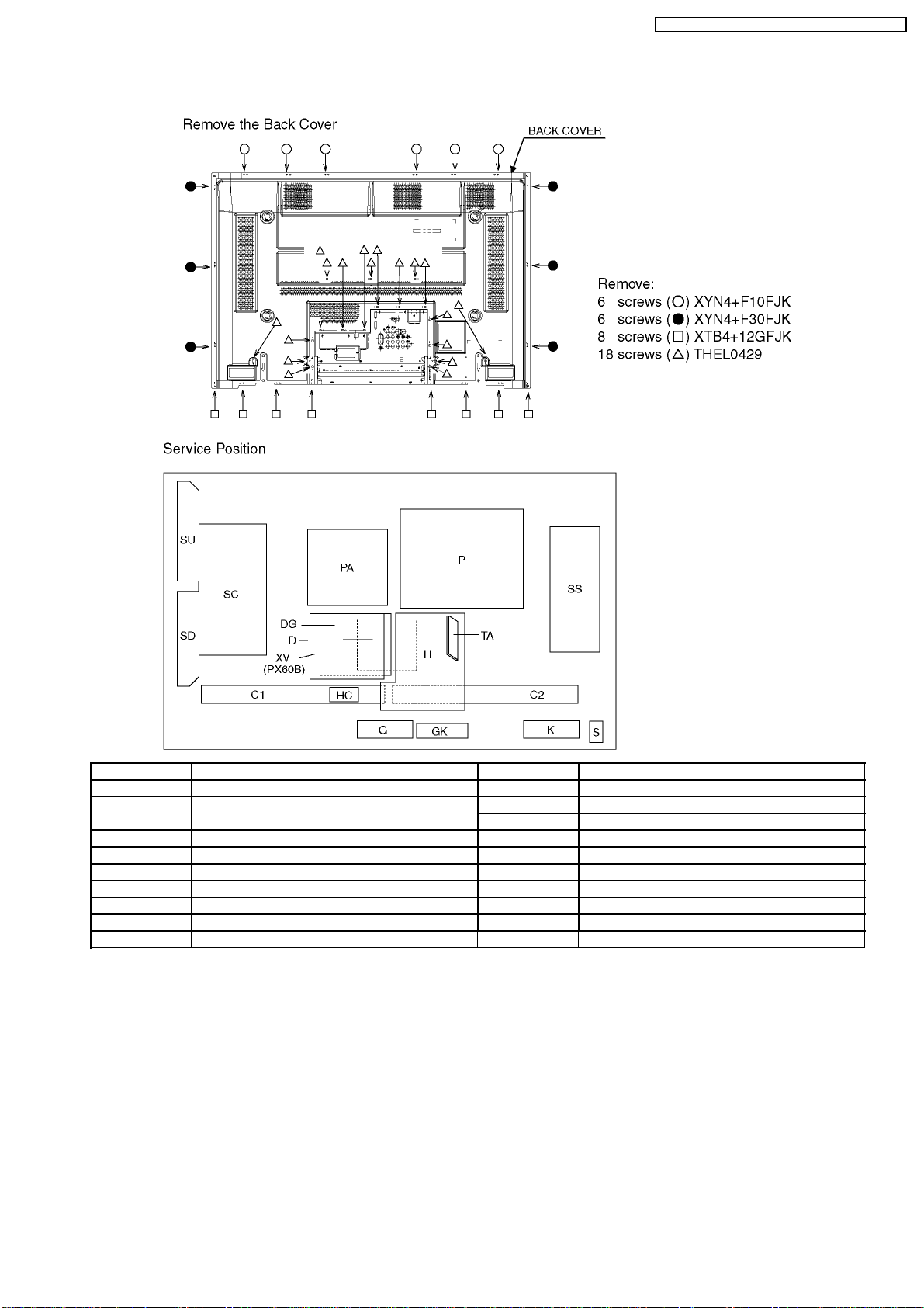
Board Name Function Board Name Function
P Power Supply C1 Data Driver (Lower Right)
PA DC-DC Converter, Speaker out, Audio AMP,
Fan Control
H AV Terminal, AV Switch, MSP SU Scan out (Upper)
TA Tuner SD Scan out (Lower)
DG Digital Signal Processor, Micom, HDMI Interface SS Sustain Drive
XV D-TV Interface (PX60B only) K Remote receiver, Power LED
D Format Converter, Plasma AI, Sub-Field Processor S Power Switch
HC Jig Connection G Front Terminal
C2 Data Driver (Lower Left)
SC Scan Drive
GK Key Switch
9
TH-37PV60E / TH-37PX60B / TH-42PV60E / TH-42PX60B
6 Plasma panel replacement method
6.1. Remove the Back cover
1. See Service Hint (Section 5)
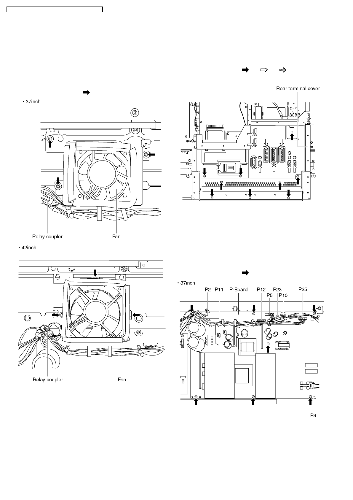
6.2. Remove the fan
1. Disconnect the relay couplers.
2. Remove the screws (×3
each) and remove the fans.
6.3. Remove the rear terminal
cover
1. Remove the screws (×9 ,×8 ,×2 ).
2. Remove the rear terminal cover.
6.4. Remove the P-Board
Caution:
To remove P.C.B. wait 1 minute after power was off for
discharge from electrolysis capacitors.
1. Unlock the cable clampers to free the cable.
2. Disconnect the couplers (P2, P5, P9, P10, P11, P12, P23,
and P25).
3. Remove the screws (×7
) and remove the P-Board.
10
TH-37PV60E / TH-37PX60B / TH-42PV60E / TH-42PX60B
6.6. Remove the tuner unit
1. Unlock the cable clampers to free the cable.
2. Disconnect the couplers (DG5, G51 and PA40).
3. Disconnect the flexible cables (DG3 and PA20).
4. Remove the screws (×4
) remove the tuner unit.
6.5. Remove the PA-Board
1. Unlock the cable clampers to free the cable.
2. Disconnect the couplers (PA2, PA5, PA10, PA31, PA32,
PA33, PA34 and PA40).
3. Disconnect the flexible cable (PA20).
4. Remove the screws (×4
5. Remove the PA-Board.
) and remove the earth cable.
6.7. Remove the XV-Board (PX60B)
1. Unlock the cable clampers to free the cable.
2. Disconnect the tuner cable.
3. Remove the screws (×5
(Be careful the couplers (XV01-DG22) when remove the
XV-Board.)
) remove the XV-Board.
11
TH-37PV60E / TH-37PX60B / TH-42PV60E / TH-42PX60B
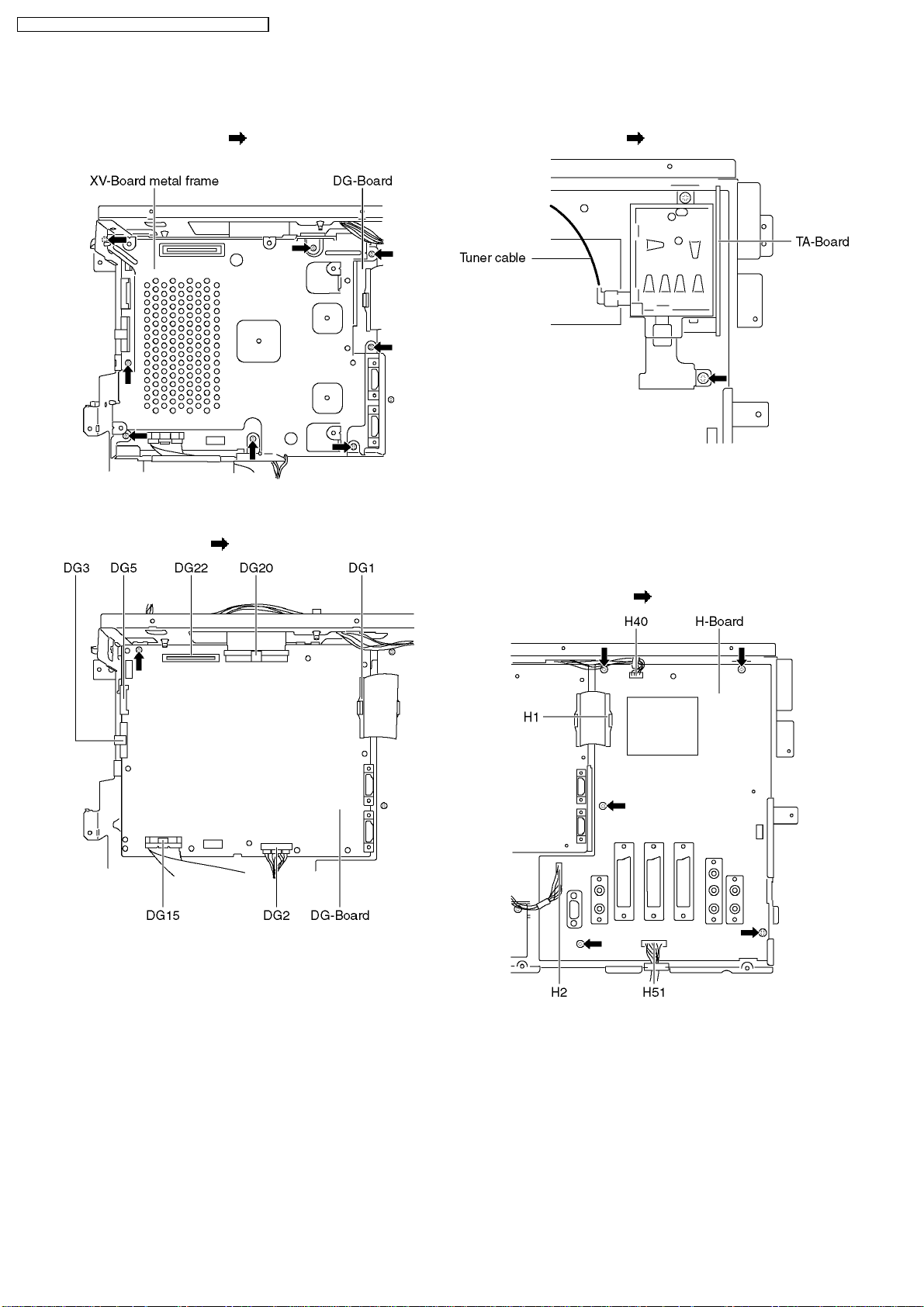
6.8. Remove the DG-Board
1. Remove the XV-Board (PX60B). (See section 6.7.)
2. Remove the screws (×8
metal frame (PX60B).
3. Disconnect the coupler (DG2).
4. Disconnect the flexible cables (DG1, DG15 and DG20).
5. Remove the screw (×1
) and remove the XV-Board
) remove the DG-Board.
6.9. Remove the TA-Board
1. Disconnect the tuner cable.
2. Remove the screw (×1
) and remove the TA-Board.
6.10. Remove the H-Board
1. Remove the TA-Board.
2. Unlock the cable clampers to free the cable.
3. Disconnect the couplers (H2, H40 and H51).
4. Disconnect the flexible cable (H1).
5. Remove the screws (×5
) and remove the H-Board.
12
TH-37PV60E / TH-37PX60B / TH-42PV60E / TH-42PX60B
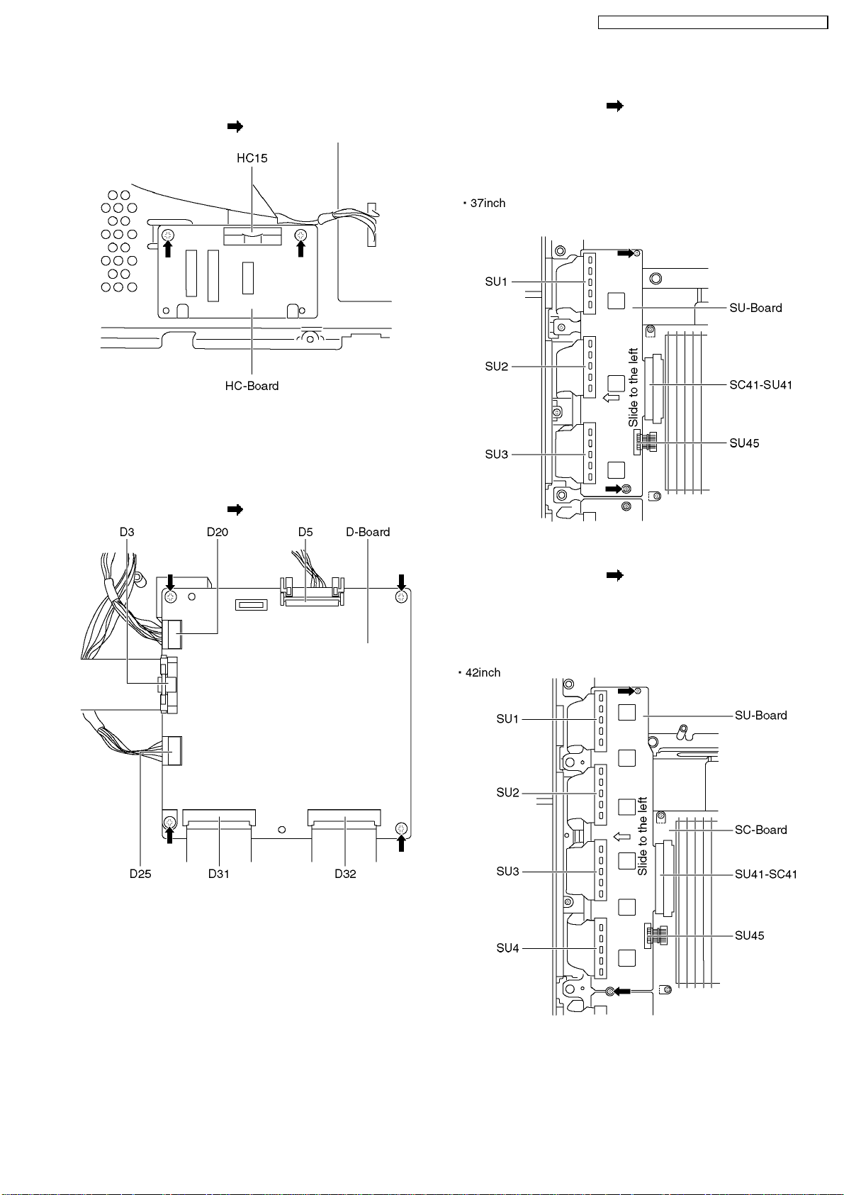
6.11. Remove the HC-Board
1. Disconnect the flexible cable (HC15).
2. Remove the screws (×2
) and remove the HC-Board.
6.12. Remove the D-Board
1. Remove the tuner unit. (See section 6.6.)
2. Disconnect the couplers (D5, D20 and D25).
3. Disconnect the flexible cables (D3, D31 and D32).
4. Remove the screws (×4
) and remove the D-Board.
6.13. Remove the SU-Board (37inch)
1. Remove the screws (×2 ).
2. Remove the flexible cables (SU1, SU2 and SU3) and
remove the bridge connector (SU45).
3. Slide the SU-Board to the left to disconnect from a coupler
(SC41-SU41) on the SC-Board and remove the SU-Board.
6.14. Remove the SU-Board (42inch)
1. Remove the screws (×2 ).
2. Remove the flexible cables (SU1, SU2, SU3 and SU4) and
remove the bridge connector (SU45).
3. Slide the SU-Board to the left to disconnect from a coupler
(SC41-SU41) on the SC-Board and remove the SU-Board.
13
TH-37PV60E / TH-37PX60B / TH-42PV60E / TH-42PX60B
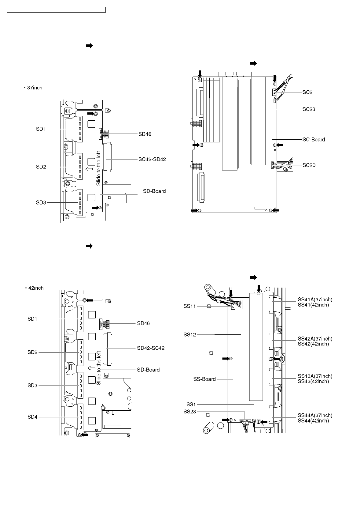
6.15. Remove the SD-Board (37inch)
1. Remove the screws (×2 ).
2. Remove the flexible cables (SD1, SD2 and SD3) and
remove the bridge connector (SD46).
3. Slide the SD-Board to the left to disconnect from a coupler
(SC42-SD42) on the SC-Board and remove the SD-Board.
6.17. Remove the SC-Board
1. Unlock the cable clampers to free the cable.
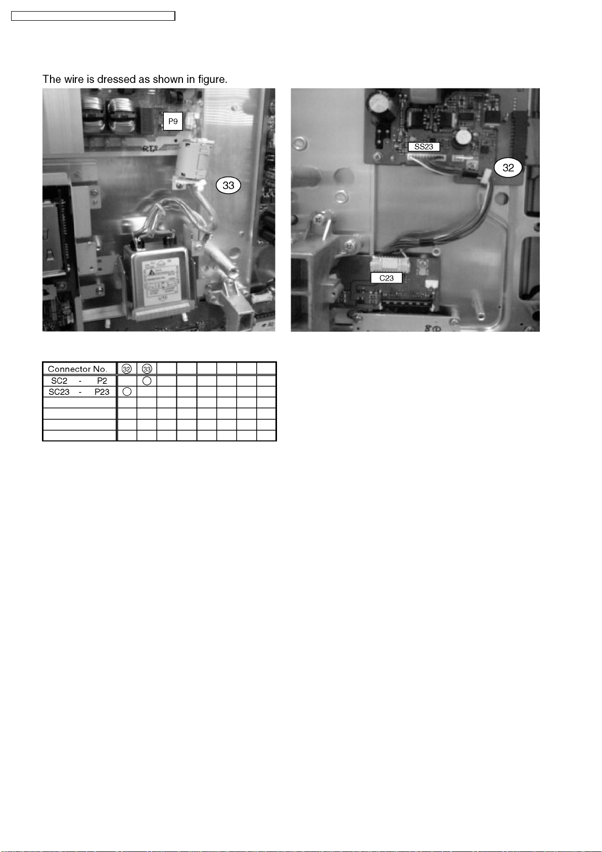
2. Disconnect the couplers (SC2, SC20 and SC23).
3. Remove the screws (×6
) and remove the SC-Board.
6.16. Remove the SD-Board (42inch)
1. Remove the screws (×2 ).
2. Remove the flexible cables (SD1, SD2, SD3 and SD4) and
remove the bridge connector (SD46).
3. Slide the SD-Board to the left to disconnect from a coupler
(SC42-SD42) on the SC-Board and remove the SD-Board.
6.18. Remove the SS-Board
1. Disconnect the couplers (SS1, SS11, SS12 and SS23).
2. Disconnect the flexible cables (SS41A, SS42A, SS43A and
SS44A) (37inch).
Disconnect the flexible cables (SS41, SS42, SS43 and
SS44) (42inch).
3. Remove the screws (×6
) and remove the SS-Board.
14
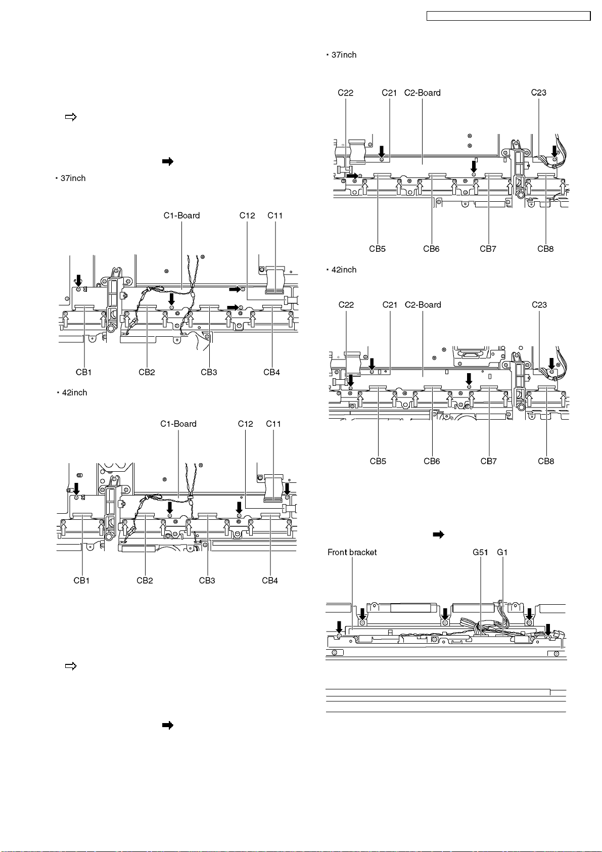
6.19. Remove the C1-Board
1. Remove the tuner unit. (See section 6.6.)
2. Unlock the cable clampers to free the cable.
3. Remove the flexible cables holder fastening screws (×8
).
4. Disconnect the flexible cables (CB1, CB2, CB3 and CB4).
5. Disconnect the flexible cables (C11 and C12).
6. Remove the screws (×4
) and remove the C1-Board.
TH-37PV60E / TH-37PX60B / TH-42PV60E / TH-42PX60B
6.20. Remove the C2-Board
1. Remove the tuner unit. (See section 6.6.)
2. Unlock the cable clampers to free the cable.
3. Remove the flexible cables holder fastening screws (×8
).
4. Disconnect the flexible cables (CB5, CB6, CB7 and CB8).
5. Disconnect the flexible cables (C21 and C22).
6. Disconnect the coupler (C23).
7. Remove the screws (×4
) and remove the C2-Board.
6.21. Remove the front bracket
1. Unlock the cable clampers to free the cable.
2. Disconnect the couplers (G1 and G51).
3. Remove the screws (×5
) and remove the front bracket.
15
TH-37PV60E / TH-37PX60B / TH-42PV60E / TH-42PX60B
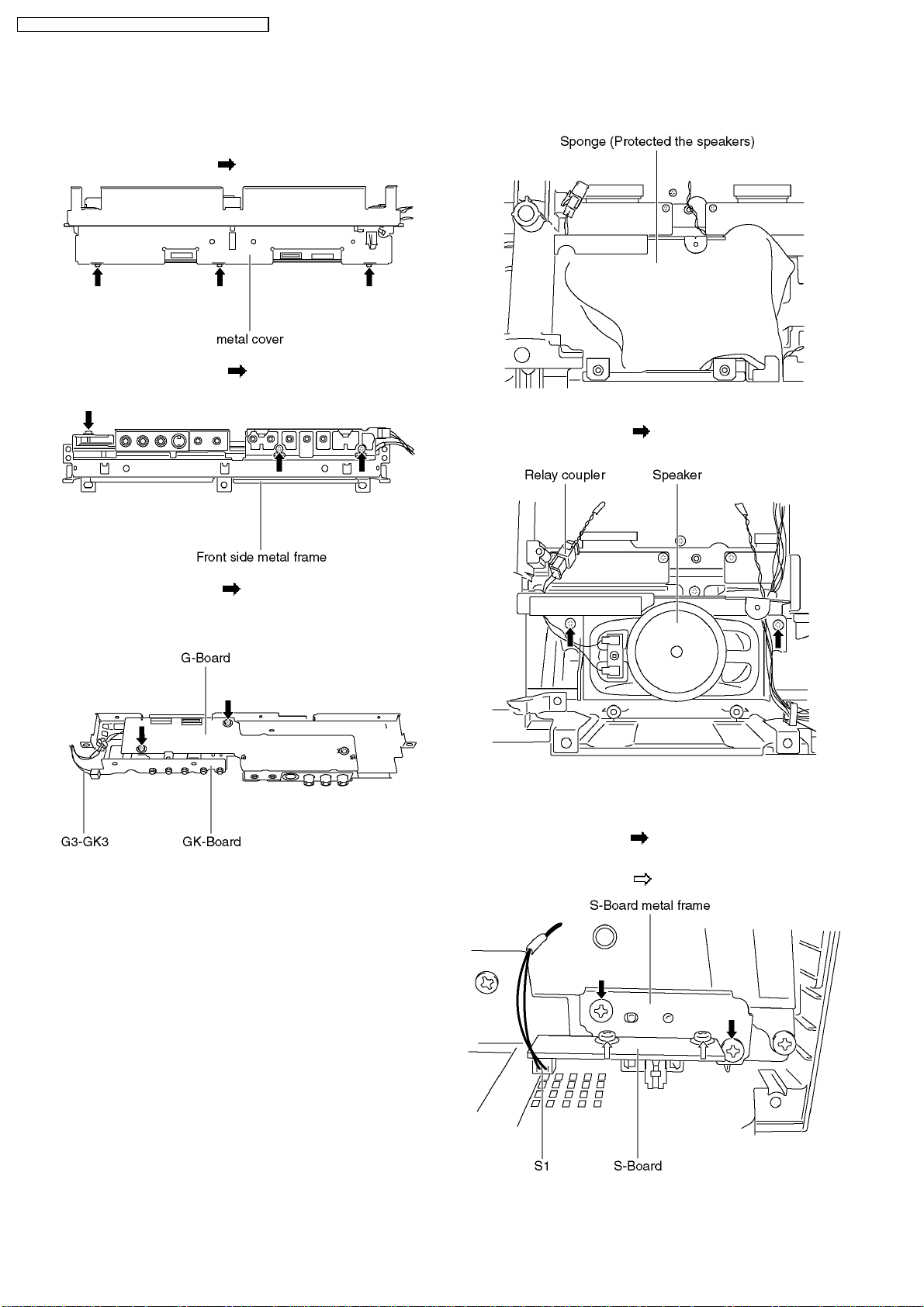
6.22. Remove the G-Board and GKBoard
1. Remove the front bracket. (See section 6.21.)
2. Remove the screws (×3
3. Remove the screws (×3 ) and remove the front side
metal frame.
) and remove the metal cover.
6.23. Remove the speaker L, R
1. Remove the sponge
2. Disconnect the relay couplers
3. Remove the screws (×2
L, R.
each) and remove the speaker
4. Remove the screws (×3 ) and disconnect the couplers
(G3-GK3).
5. Remove the G-Board and GK-Board.
6.24. Remove the S-Board
1. Disconnect the coupler (S1).
2. Remove the screws(×2
frame.
3. Remove the screws (×2
) and remove the S-Board metal
) and remove the S-Board.
16
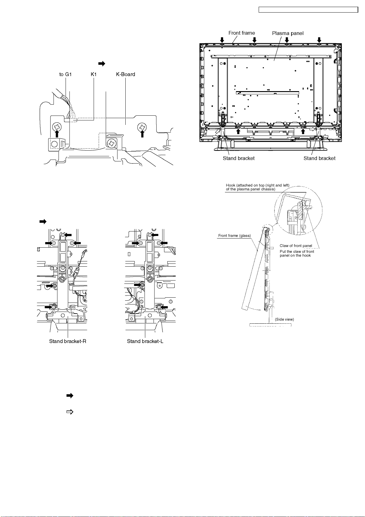
6.25. Remove the K-Board
1. Unlock the cable clampers to free the cable.
2. Disconnect the coupler (G1). (See section 6.21.)
3. Remove the screws (×2
) and remove the K-Board.
6.26. Remove the stand brackets
TH-37PV60E / TH-37PX60B / TH-42PV60E / TH-42PX60B
3. For leaving the plasma panel from the front frame, pull the
bottom of the front frame forward, lift, and remove.
1. Remove the plasma panel section from the servicing stand
and lay on a fiat surface such as a table (covered) with the
plasma panel surface facing downward.
2. Remove the stand brackets (left, right)fastening screws (×5
each) and remove the stand brackets (left, right).
6.27. Remove the Plasma panel
section from the Front frame
(glass)
1. Remove the front frame and the plasma panel fastening
screws (×6
2. Remove the front frame and the stand brackets fastening
screws (×4
).
).
6.28. Replace the plasma panel
(finished)
1. Place the new plasma panel (finished) on the flat surface of
the table (covered by a soft cloth), with the plasma panel
surface facing downward.
2. Attach the C1-Board and the C2-Board, connect the flexible
cables (×8) from the Plasma panel to the C1-Board and the
C2-Board, and fit the flexible cable holders.
3. Attach the Hooks (left, right) and fit the stand brackets (L,
R) to the new plasma panel.
4. Place the plasma panel section on the servicing stand.
5. Attach the front frame and each P.C.Board and so on, to
the new plasma panel.
* When fitting the front frame, be careful to allow any
debris, dust or handling residue to remain between the
front glass and plasma panel.
17
TH-37PV60E / TH-37PX60B / TH-42PV60E / TH-42PX60B
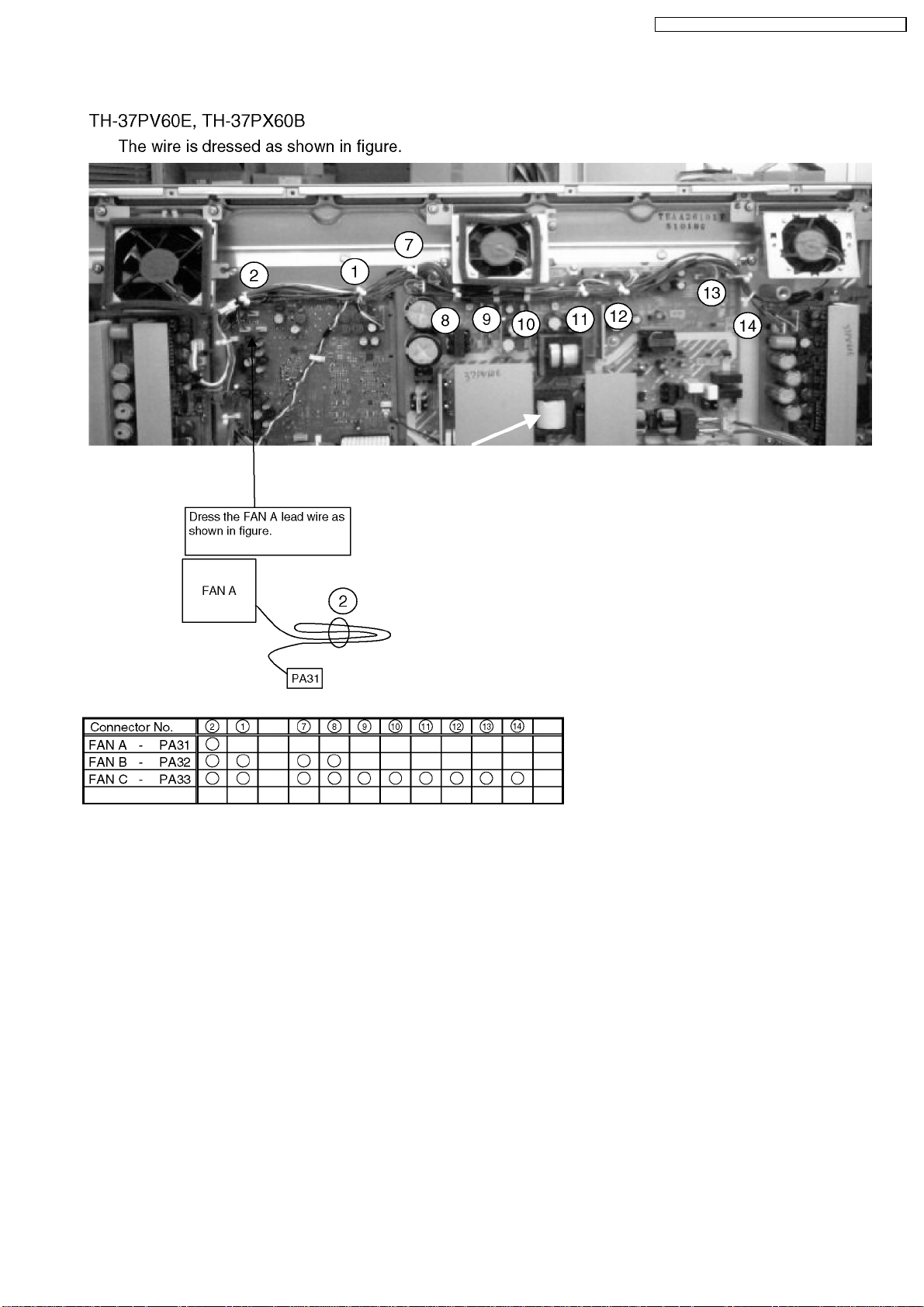
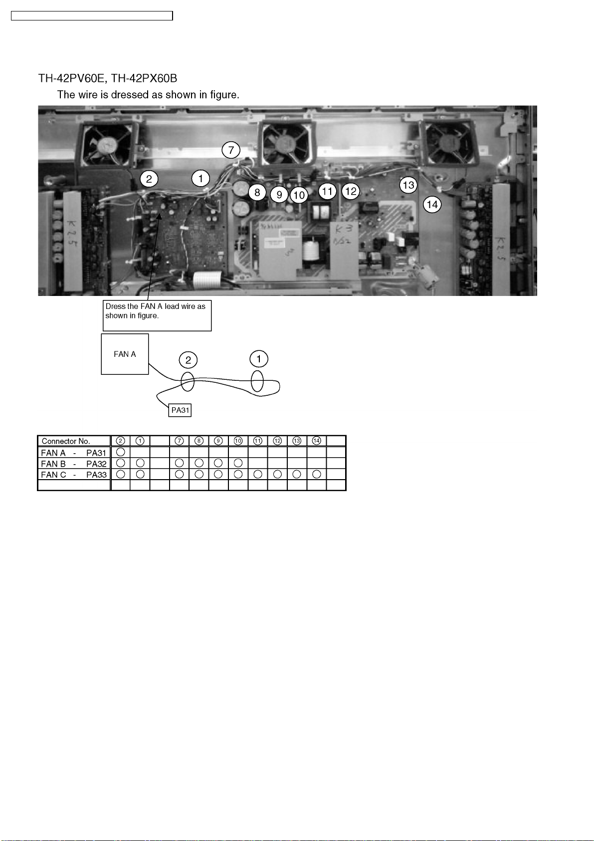
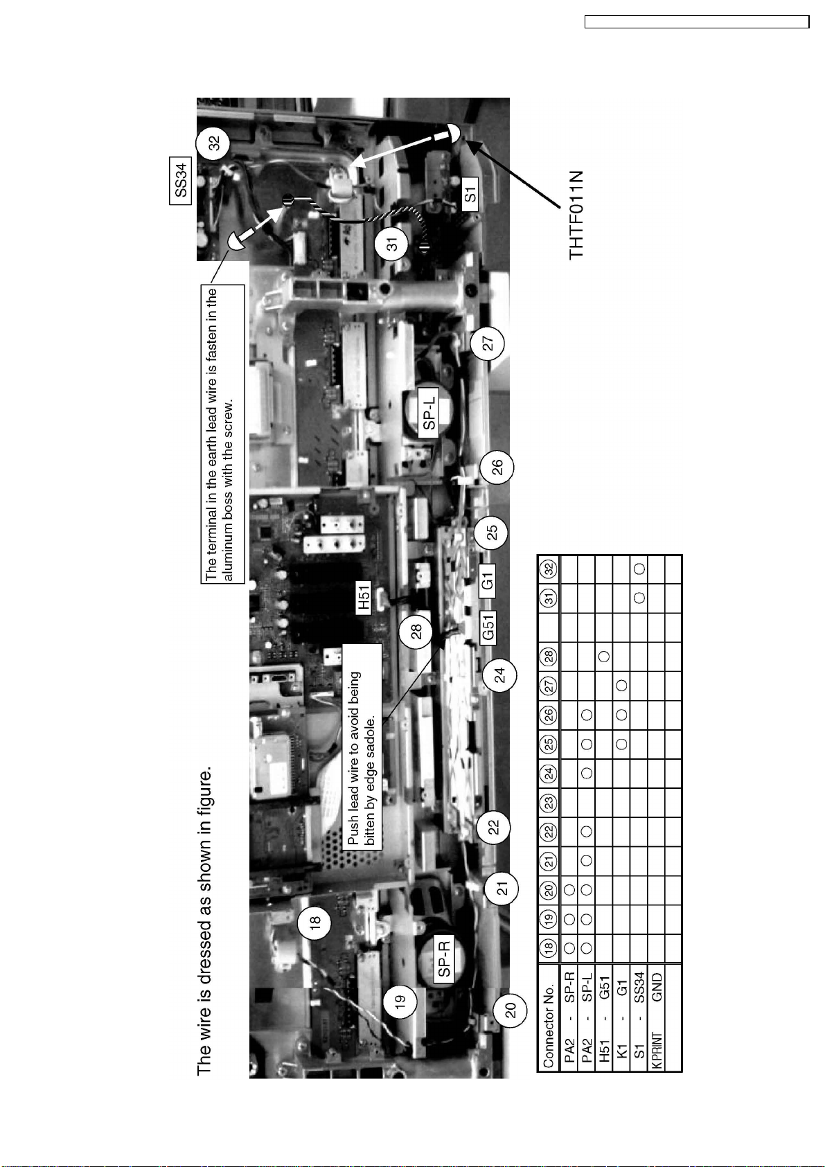
7 Location of Lead Wiring
7.1. Lead of Wiring (1)
18
7.2. Lead of Wiring (2)
TH-37PV60E / TH-37PX60B / TH-42PV60E / TH-42PX60B
19
TH-37PV60E / TH-37PX60B / TH-42PV60E / TH-42PX60B
7.3. Lead of Wiring (3)
20
7.4. Lead of Wiring (4)
TH-37PV60E / TH-37PX60B / TH-42PV60E / TH-42PX60B
21
TH-37PV60E / TH-37PX60B / TH-42PV60E / TH-42PX60B
7.5. Lead of Wiring (5)
22
7.6. Lead of Wiring (6)
TH-37PV60E / TH-37PX60B / TH-42PV60E / TH-42PX60B
23
TH-37PV60E / TH-37PX60B / TH-42PV60E / TH-42PX60B
7.7. Lead of Wiring (7)
24
7.8. Lead of Wiring (8)
TH-37PV60E / TH-37PX60B / TH-42PV60E / TH-42PX60B
25
TH-37PV60E / TH-37PX60B / TH-42PV60E / TH-42PX60B
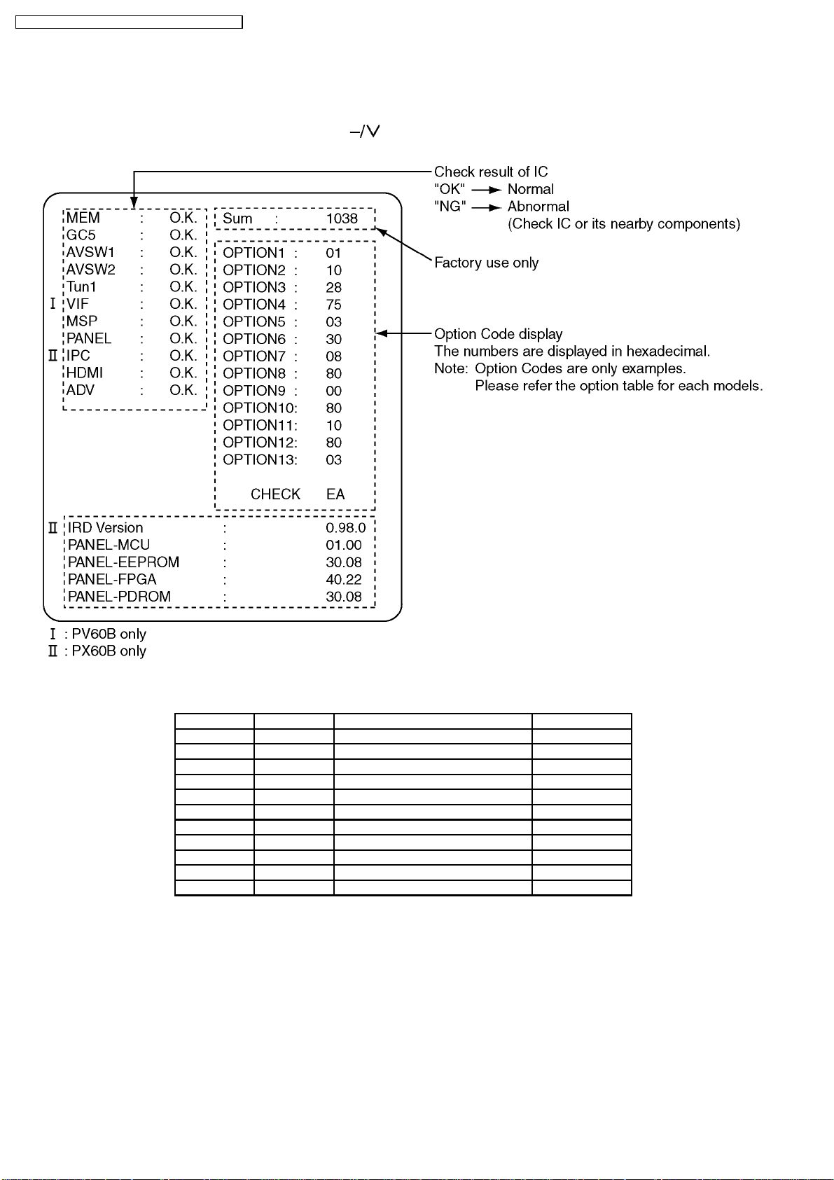
8 Self Check
1. Self-Check is used to automatically check the bus lines and hexadecimal code of the TV set.
2. To get into the Self -Check mode press the Down (
time pressing the Information button on the remote control, and the screen will show :
) button on the customer controls at the front of the set, at the same
If the CCU ports have been checked and found to be incorrect or not located then “--” will appear in place of “O.K.”.
Display Ref.No. Description Board
MEM IC1102 EEPROM DG-Board
GC5 IC4037 GC5 Processor DG-Board
AVSW1 IC3005 Video SW H-Board
AVSW2 IC2105 Audio SW H-Board
Tun1 TU001 Tuner TA-Board
VIF - - MSP IC2106 Multi Sound Processor H-Board
PANEL IC9003 Convert Micon D-Board
IPC IC8013 PEAKS Lite XV-Board
HDMI IC4026 HDMI I/F Receiver DG-Board
ADV IC4019 10bit A/D DG-Board
26
TH-37PV60E / TH-37PX60B / TH-42PV60E / TH-42PX60B
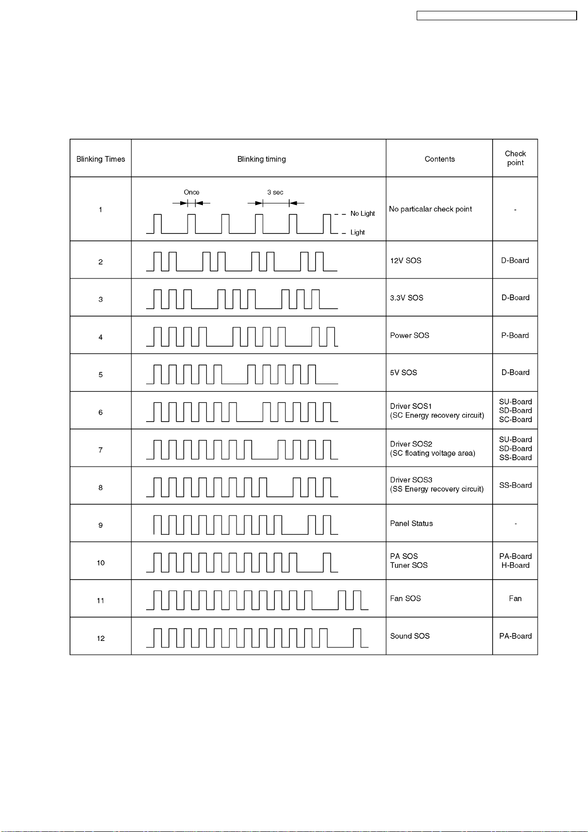
8.1. Power LED Blinking timing chart
1. Subject
Information of LED Flashing timing chart.
2. Contents
When an abnormality has occurred the unit, the protection circuit operates and reset to the stand by mode. At this time, the
defective block can be identified by the number of blinkes of the Power LED on the front panel of the unit.
27
TH-37PV60E / TH-37PX60B / TH-42PV60E / TH-42PX60B
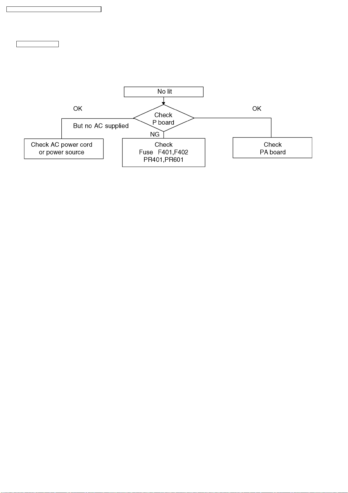
8.2. No Power
First check point
There are following 3 states of No Power indication by power LED.
1. No lit
2. Green is lit then turns red blinking a few seconds later.
3. Only red is lit.
28
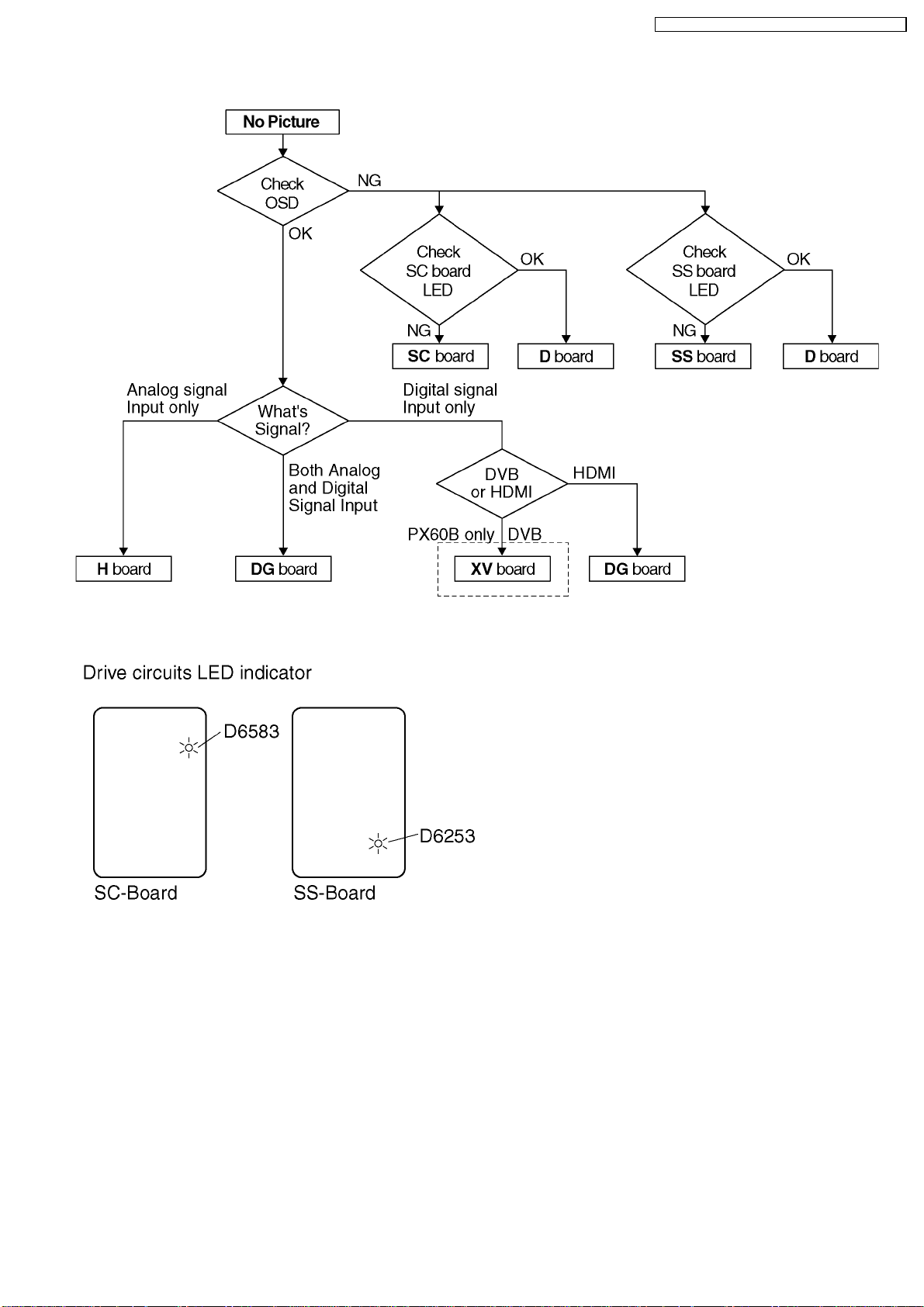
8.3. No Picture
TH-37PV60E / TH-37PX60B / TH-42PV60E / TH-42PX60B
29
TH-37PV60E / TH-37PX60B / TH-42PV60E / TH-42PX60B
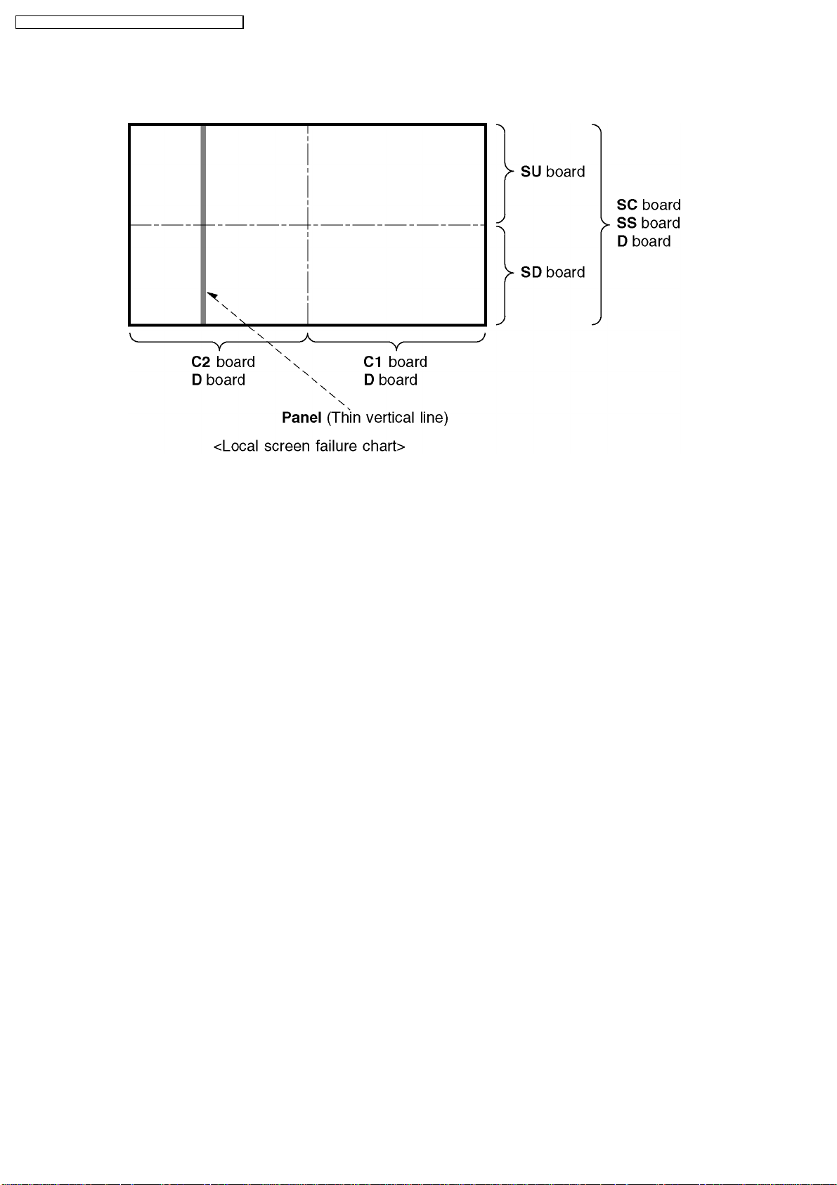
8.4. Local screen failure
Plasma display may have local area failure on the screen. Fig-1 is the possible defect P.C.B. for each local area.
Fig-1
30
 Loading...