

Page 1

ORDER NO.MTNC090103CE
B34 Canada: B07
42 inch Class 720p Plasma HDTV
Model No. TC-P42C1
GPH12DU Chassis
© Panasonic Corporation 2009.
Unauthorized copying and distribution is a violation
of law.
Page 2

1 Safety Precautions
1.1. General Guidelines
1. When conducting repairs and servicing, do not attempt to modify the equipment, its parts or its materials.
2. When wiring units (with cables, flexible cables or lead wires) are supplied as repair parts and only one wire or some of the
wires have been broken or disconnected, do not attempt to repair or re-wire the units. Replace the entire wiring unit instead.
3. When conducting repairs and servicing, do not twist the Faston connectors but plug them straight in or unplug them straight
out.
4. When servicing, observe the original lead dress. If a short circuit is found, replace all parts which have been overheated or
damaged by the short circuit.
5. After servicing, see to it that all the protective devices such as insulation barriers, insulation papers shields are properly
installed.
6. After servicing, make the following leakage current checks to prevent the customer from being exposed to shock hazards.
1.1.1. Leakage Current Cold Check
1. Unplug the AC cord and connect a jumper between the
two prongs on the plug.
2. Measure the resistance value, with an ohmmeter,
between the jumpered AC plug and each exposed metallic cabinet part on the equipment such as screwheads,
connectors, control shafts, etc. When the exposed metallic part has a return path to the chassis, the reading
should be between 1Mohm and 5.2Mohm.
When the exposed metal does not have a return path to
the chassis, the reading must be .
1.1.2. Leakage Current Hot Check (See
Figure 1.)
1. Plug the AC cord directly into the AC outlet. Do not use
an isolation transformer for this check.
2. Connect a 1.5kohm, 10 watts resistor, in parallel with a
0.15μF capacitors, between each exposed metallic part
on the set and a good earth ground such as a water pipe,
as shown in Figure 1.
3. Use an AC voltmeter, with 1000 ohms/volt or more sensitivity, to measure the potential across the resistor.
4. Check each exposed metallic part, and measure the voltage at each point.
5. Reverse the AC plug in the AC outlet and repeat each of
the above measurements.
6. The potential at any point should not exceed 0.75 volts
RMS. A leakage current tester (Simpson Model 229 or
equivalent) may be used to make the hot checks, leakage
current must not exceed 1/2 milliamp. In case a measurement is outside of the limits specified, there is a possibility
of a shock hazard, and the equipment should be repaired
and rechecked before it is returned to the customer.
Figure 1
2
Page 3

2Warning
2.1. Prevention of Electrostatic Discharge (ESD) to Electrostatically
Sensitive (ES) Devices
Some semiconductor (solid state) devices can be damaged easily by static electricity. Such components commonly are called Electrostatically Sensitive (ES) Devices. Examples of typical ES devices are integrated circuits and some field-effect transistors and
semiconductor [chip] components. The following techniques should be used to help reduce the incidence of component damage
caused by electrostatic discharge (ESD).
1. Immediately before handling any semiconductor component or semiconductor-equipped assembly, drain off any ESD on your
body by touching a known earth ground. Alternatively, obtain and wear a commercially available discharging ESD wrist strap,
which should be removed for potential shock reasons prior to applying power to the unit under test.
2. After removing an electrical assembly equipped with ES devices, place the assembly on a conductive surface such as aluminum foil, to prevent electrostatic charge buildup or exposure of the assembly.
3. Use only a grounded-tip soldering iron to solder or unsolder ES devices.
4. Use only an anti-static solder removal device. Some solder removal devices not classified as [anti-static (ESD protected)] can
generate electrical charge sufficient to damage ES devices.
5. Do not use freon-propelled chemicals. These can generate electrical charges sufficient to damage ES devices.
6. Do not remove a replacement ES device from its protective package until immediately before you are ready to install it. (Most
replacement ES devices are packaged with leads electrically shorted together by conductive foam, aluminum foil or comparable conductive material).
7. Immediately before removing the protective material from the leads of a replacement ES device, touch the protective material
to the chassis or circuit assembly into which the device will be installed.
Caution
Be sure no power is applied to the chassis or circuit, and observe all other safety precautions.
8. Minimize bodily motions when handling unpackaged replacement ES devices. (Otherwise ham less motion such as the brushing together of your clothes fabric or the lifting of your foot from a carpeted floor can generate static electricity (ESD) sufficient
to damage an ES device).
3
Page 4
2.2. About lead free solder (PbF)
Note: Lead is listed as (Pb) in the periodic table of elements.
In the information below, Pb will refer to Lead solder, and PbF will refer to Lead Free Solder.
The Lead Free Solder used in our manufacturing process and discussed below is (Sn+Ag+Cu).
That is Tin (Sn), Silver (Ag) and Copper (Cu) although other types are available.
This model uses Pb Free solder in it’s manufacture due to environmental conservation issues. For service and repair work, we’d
suggest the use of Pb free solder as well, although Pb solder may be used.
PCBs manufactured using lead free solder will have the PbF within a leaf Symbol PbF stamped on the back of PCB.
Caution
• Pb free solder has a higher melting point than standard solder. Typically the melting point is 50 ~ 70 °F (30~40 °C) higher. Please
use a high temperature soldering iron and set it to 700 ± 20 °F (370 ± 10 °C).
• Pb free solder will tend to splash when heated too high (about 1100 °F or 600 °C).
If you must use Pb solder, please completely remove all of the Pb free solder on the pins or solder area before applying Pb solder. If this is not practical, be sure to heat the Pb free solder until it melts, before applying Pb solder.
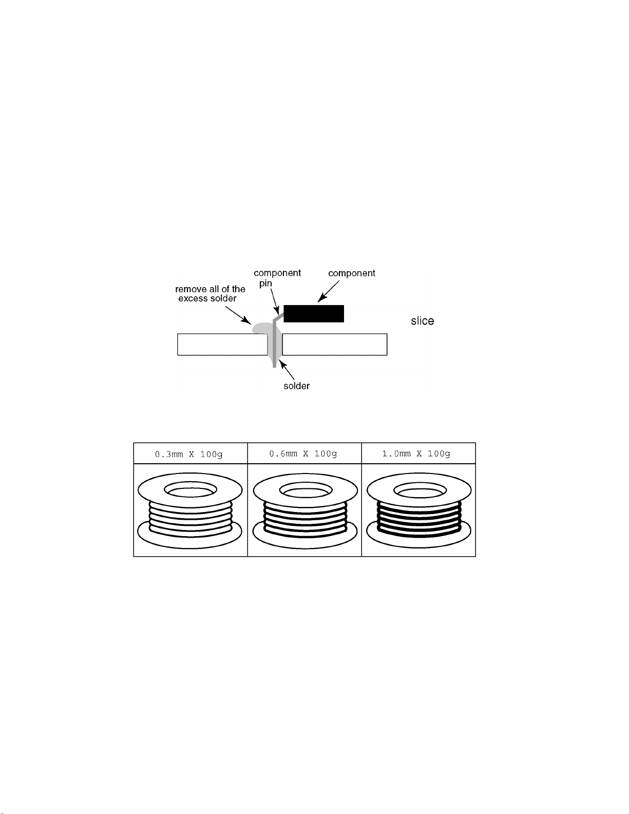
• After applying PbF solder to double layered boards, please check the component side for excess solder which may flow onto the
opposite side. (see figure below)
Suggested Pb free solder
There are several kinds of Pb free solder available for purchase. This product uses Sn+Ag+Cu (tin, silver, copper) solder. However, Sn+Cu (tin, copper), Sn+Zn+Bi (tin, zinc, bismuth) solder can also be used.
4
Page 5

3 Service Navigation
3.1. Service Hint
Board Name Function Board Name Function
P Power Supply C1 Data Driver (Lower Right)
A DC-DC Converter, Tuner
Speaker out, AV Terminal, AV Switch
Digital Signal Processor, SYSTEM MPU, HDMI Switch
Seine 3LV
Format Converter, Plasma AI, Sub-Field Processor
K Remote receiver, Power LED, C.A.T.S. sensor SD Scan out (Lower)
S Power Switch
GK Key Switch
C2 Data Driver (Lower Left)
SC Scan Drive
SS Sustain Drive
SS2 Sustain out (Lower)
SU Scan out (Upper)
None serviceable.
SU-Board should be exchanged for service.
None serviceable.
SD-Board should be exchanged for service.
5
Page 6

3.2. Applicable signals
* Mark: Applicable input signal for Component (Y, PB, PR) and HDMI
horizontal frequency (kHz) vertical frequency (Hz) COMPONENT HDMI
525 (480) / 60i 15.73 59.94 * *
525 (480) /60p 31.47 59.94 * *
750 (720) /60p 45.00 59.94 * *
1,125 (1,080) /60i 33.75 59.94 * *
1,125 (1,080)/60p 67.43 59.94 *
1,125 (1,080)/60p 67.50 60.00 *
1,125(1,080)/24p 26.97 23.98 *
1,125(1,080)/24p 27.00 24.00 *
Note
• Signals other than those shown above may not be displayed properly.
• The above signals are reformatted for optimal viewing on your display.
6
Page 7

4 Specifications
Power Source AC 120 V, 60 Hz
Power Consumption
Maximum 283 W
Standby condition 0.3 W
Plasma Display panel
Drive method AC type
Aspect Ratio 16:9
Visible screen size 42 inch class (41.6 inches measured diagonally)
(W × H × Diagonal) 36.2 inch × 20.4 inch × 41.6 inch (921 mm × 518 mm × 1,057 mm)
(No. of pixels) 786,432 (1,024 (W) × 768 (H))[3,072 × 768 dots]
Sound
Audio Output 20 W [ 10 W + 10 W ] ( 10 % THD )
Channel Capability (Digital/Analog) VHF/ UHF: 2 - 69, CATV: 1 - 135
Operating Conditions
Temperature: 32 °F - 104 °F (0 °C - 40 °C)
Humidity: 20 % - 80 % RH (non-condensing)
Connection Terminals
VIDEO IN 1 VIDEO: RCA PIN Type × 1 1.0 V [p-p] (75 Ω)
S-VIDEO: Mini DIN 4-pin Y: 1.0 V [p-p] (75 Ω) C: 0.286 V [p-p] (75 Ω)
AUDIO L-R: RCA PIN Type × 2 0.5 V [rms]
VIDEO IN 2 VIDEO: RCA PIN Type × 1 1.0 V [p-p] (75 Ω)
AUDIO L-R: RCA PIN Type × 2 0.5 V [rms]
COMPONENT IN 1-2 Y: 1.0 V [p-p] (including synchronization)
PB, PR: ±0.35 V [p-p]
AUDIO L-R: RCA PIN Type × 2 0.5 V [rms]
HDMI 1-2 TYPE A Connector × 2
This TV supports [HDAVI Control 4] function.
Card slot SD CARD slot × 1
DIGITAL AUDIO OUT PCM / Dolby Digital, Fiber Optic
FEATURES 3D Y/C FILTER
CLOSED CAPTION V-Chip
Photo Viewer HDAVI Control 4
Dimensions (W × H × D)
Including pedestal 40.6 inch ×
TV Set only 40.6 inch × 26.1 inch × 3.8 inch (4.2 inch) (1,029mm × 661 mm × 94 mm (106 mm))
Mass
Including pedestal 61.8 lb. (28.0 kg)
TV Set only 57.4 lb. (26.0 kg)
28.0 inch × 12
.9 inch (1,029 mm × 709 mm × 327 mm)
Note
• Design and Specifications are subject to change without notice. Mass and Dimensions shown are approximate.
7
Page 8
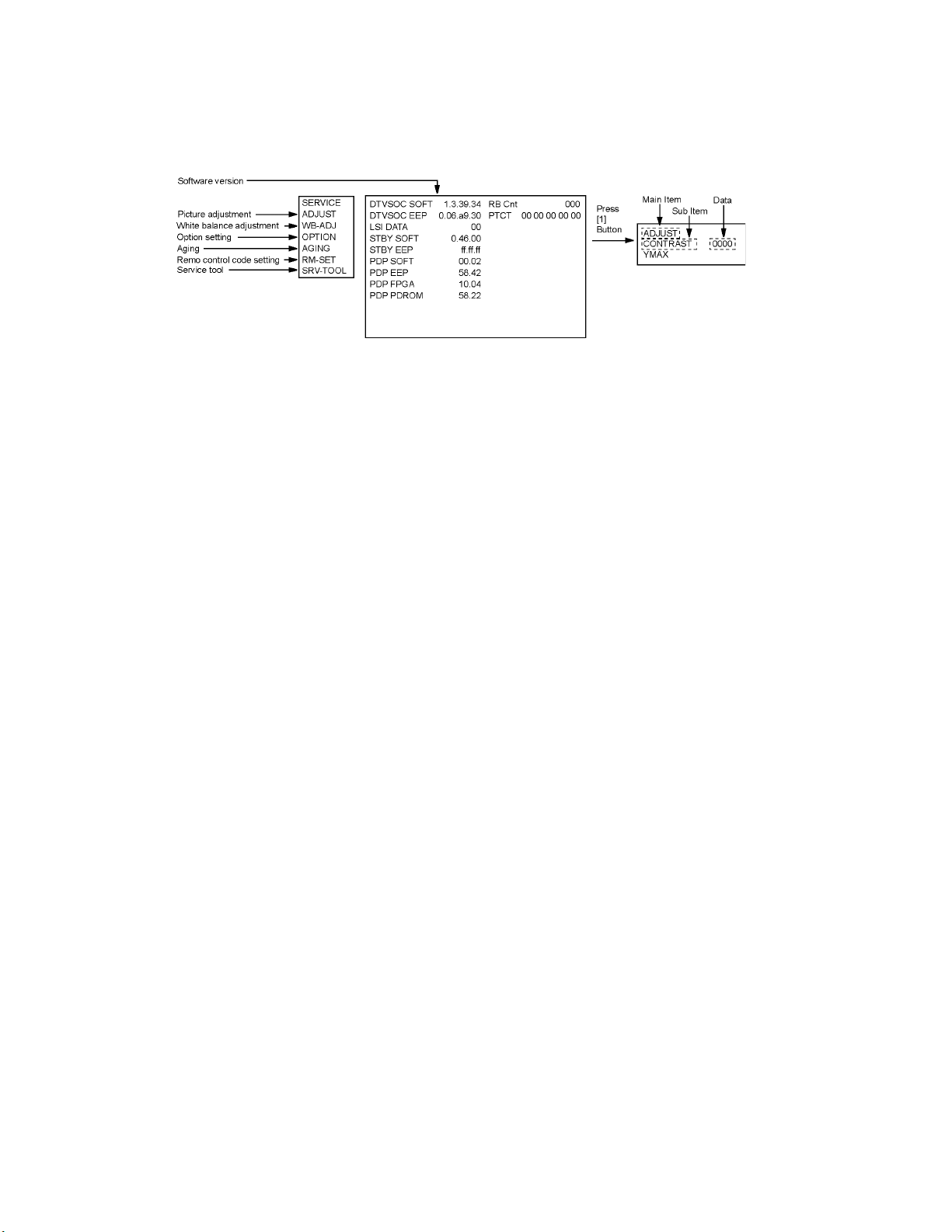
5 Service Mode
5.1. How to enter into Service Mode
While pressing [VOLUME ( - )] button of the main unit, press [INFO] button of the remote control three times within 2 seconds.
5.1.1. Key command
[1] button...Main items Selection in forward direction
[2] button...Main items Selection in reverse direction
[3] button...Sub items Selection in forward direction
[4] button...Sub items Selection in reverse direction
[VOL] button...Value of sub items change in forward direction ( + ), in reverse direction ( - )
8
Page 9
5.1.2. Contents of adjustment mode
• Value is shown as a hexadecimal number.
• Preset value differs depending on models.
• After entering the adjustment mode, take note of the value in each item before starting adjustment.
Main item Sub item Sample Data Remark
ADJUST CONTRAST 46
COLOR 00
TINT 00
SUB-BRT 000
WB-ADJ R-CUT 80
G-CUT 80
B-CUT 80
R-DRV FC
G-DRV FF
B-DRV E8
ALL-CUT 80
ALL-DRV FC
OPTION BOOT ROM Factory Preset
STBY-SET - EMERGENCY ON
CLK MODE 00
CLOCK 000
AGING RGBW
VERTICAL LINE
COUNT
ALL WHITE
ALL RED
ALL GREEN
ALL BLUE
ON/OFF
RAMP WHITE
RAMP RED
RAMP GREEN
RAMP BLUE
1% WINDOW
COLOR BAR
A-ZONE B-ZONE/4 TRIO
SCROLL
WHITE FLAME
LOW SETUP RED
LOW SETUP GREEN
LOW SETUP BLUE
RM-SET CODE A Fixed
SRV-TOOL - See next
5.1.3. How to exit
Switch off the power with the [POWER] button on the main unit or the [POWER] button on the remote control.
9
Page 10
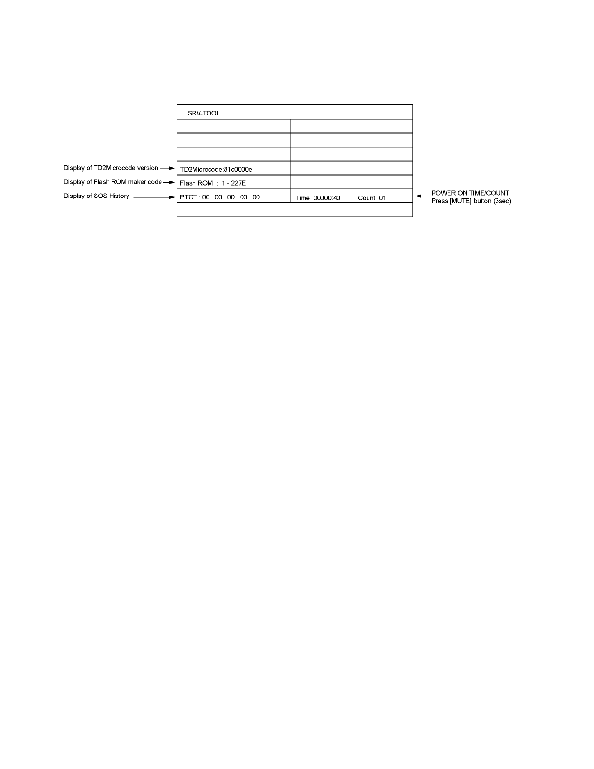
5.2. Service tool mode
5.2.1. How to access
1. Select [SRV-TOOL] in Service Mode.
2. Press [OK] button on the remote control.
5.2.2. Display of SOS History
SOS History (Number of LED blinking) indication.
From left side; Last SOS, before Last, three occurrence before, 2nd occurrence after shipment, 1st occurrence after shipment.
This indication except 2nd and 1st occurrence after shipment will be cleared by [Self-check indication and forced to factory shipment setting].
5.2.3. POWER ON TIME/COUNT
Note : To display TIME/COUNT menu, highlight position, then press MUTE for (3sec).
Time : Cumulative power on time, indicated hour : minute by decimal
Count : Number of ON times by decimal
Note : This indication will not be cleared by either of the self-checks or any other command.
5.2.4. Exit
1. Disconnect the AC cord from wall outlet.
10
Page 11

5.3. Hotel mode
1. Purpose
Restrict a function for hotels.
2. Access command to the Hotel mode setup menu
In order to display the Hotel mode setup menu, please
enter the following command (within 2 second).
[TV] : Vol. [Down] + [REMOTE] : INPUT (3 times)
Then, the Hotel mode setup menu is displayed.
3. To exit the Hotel mode setup menu
Disconnect AC power cord from wall outlet.
4. Explain the Hotel mode setup menu
item Function
Mode Select hotel mode ON/OFF
Input Select input signal modes.
Set the input, when each time power is
switched on.
Selection:
-/ANTENNA/COMP1/COMP2/HDMI1/
HDMI2/VIDEO1/VIDEO2
Off: give priority to a last memory.
Channel Select channel when input signal is RF.
Set the channel, each time power is switched
on.
Selection:
Any channel number or [-].
[-] means the channel when turns off.
Volume Adjust the volume when each time power is
switched on.
Range:
0 to 100
Vol. Max Adjust maximum volume.
Range:
0 to 100
OSD Ctrl Restrict the OSD.
Selection:
OFF/PATTERN1
• OFF: No restriction
• PATTERN1: restriction
FP Ctrl Select front key conditions.
Selection:
Off/All/Pattern1
• Off: altogether valid.
• All: altogether invalid.
• Pattern: only input key is valid.
Pow Ctrl Select POWER-ON/OFF condition when AC
power cord is disconnected and then connected.
OFF: The same condition when AC power
cord is disconnected.
ON: Forced power ON condition.
11
Page 12
6 Troubleshooting Guide
Use the self-check function to test the unit.
1. Checking the IIC bus lines
2. Power LED Blinking timing
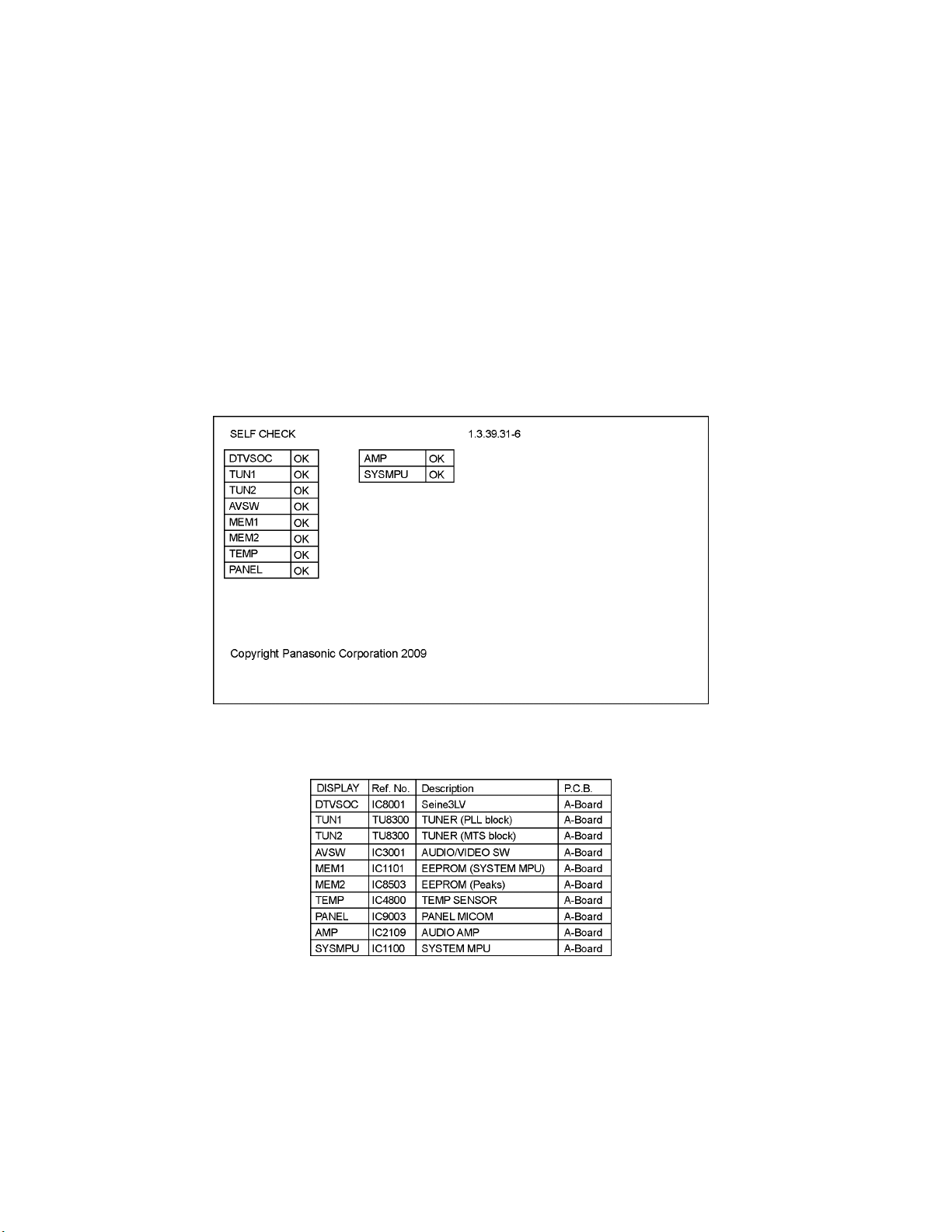
6.1. Check of the IIC bus lines
6.1.1. How to access
Self-check indication only:
Produce TV reception screen, and while pressing [VOLUME ( - )] button on the main unit, press [OK] button on the remote control
for more than 3 seconds.
Self-check indication and forced to factory shipment setting:
Produce TV reception screen, and while pressing [VOLUME ( - )] button on the main unit, press [MENU] button on the remote control for more than 3 seconds.
6.1.2. Exit
Disconnect the AC cord from wall outlet.
6.1.3. Screen display
6.1.4. Check Point
Confirm the following parts if NG was displayed.
12
Page 13

6.2. Power LED Blinking timing chart
1. Subject
Information of LED Flashing timing chart.
2. Contents
When an abnormality has occurred the unit, the protection circuit operates and reset to the stand by mode. At this time, the
defective block can be identified by the number of blinks of the Power LED on the front panel of the unit.
13
Page 14
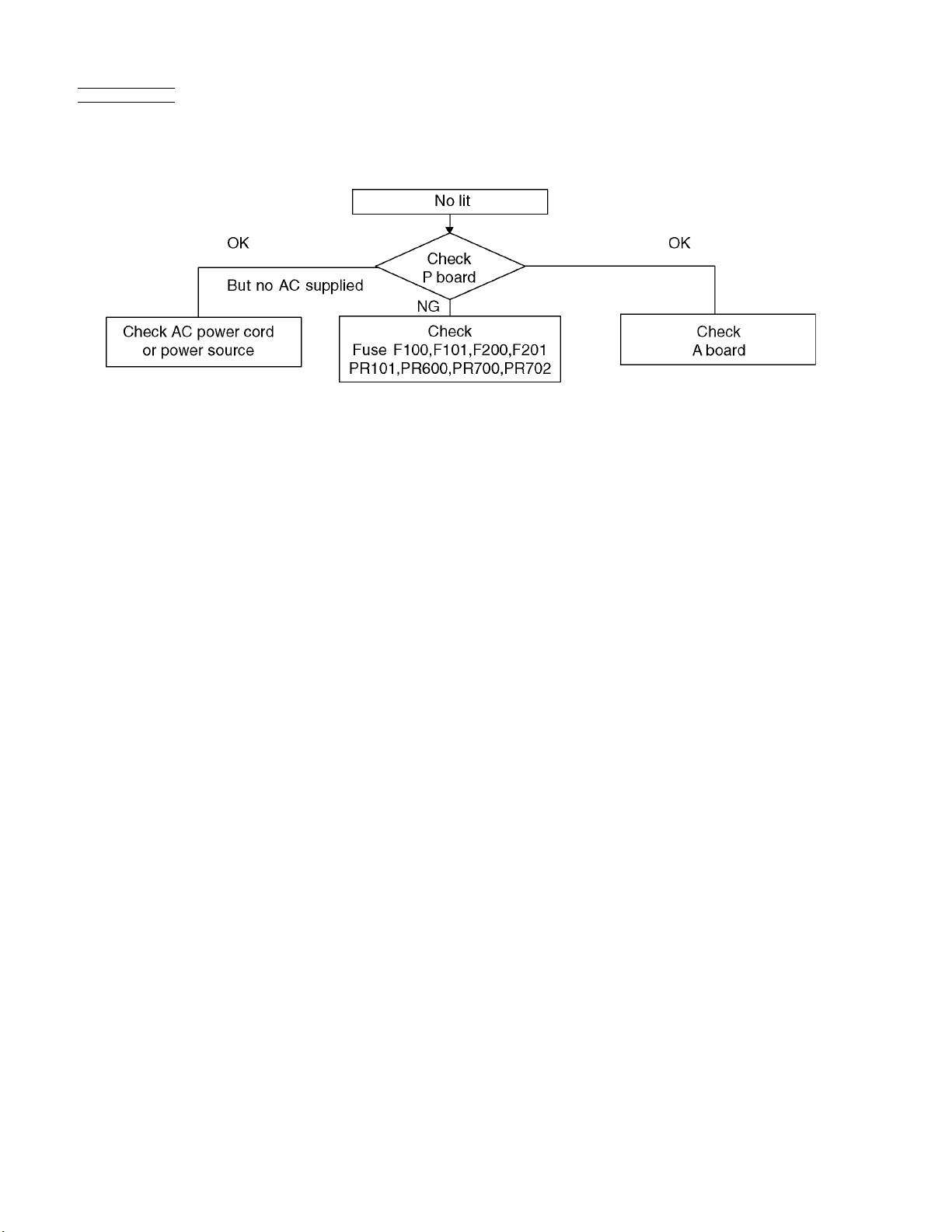
6.3. No Power
First check point
There are following 2 states of No Power indication by power LED.
1. No lit
2. Red is lit then turns red blinking a few seconds later. (See 6.2.)
14
Page 15

6.4. No Picture
15
Page 16
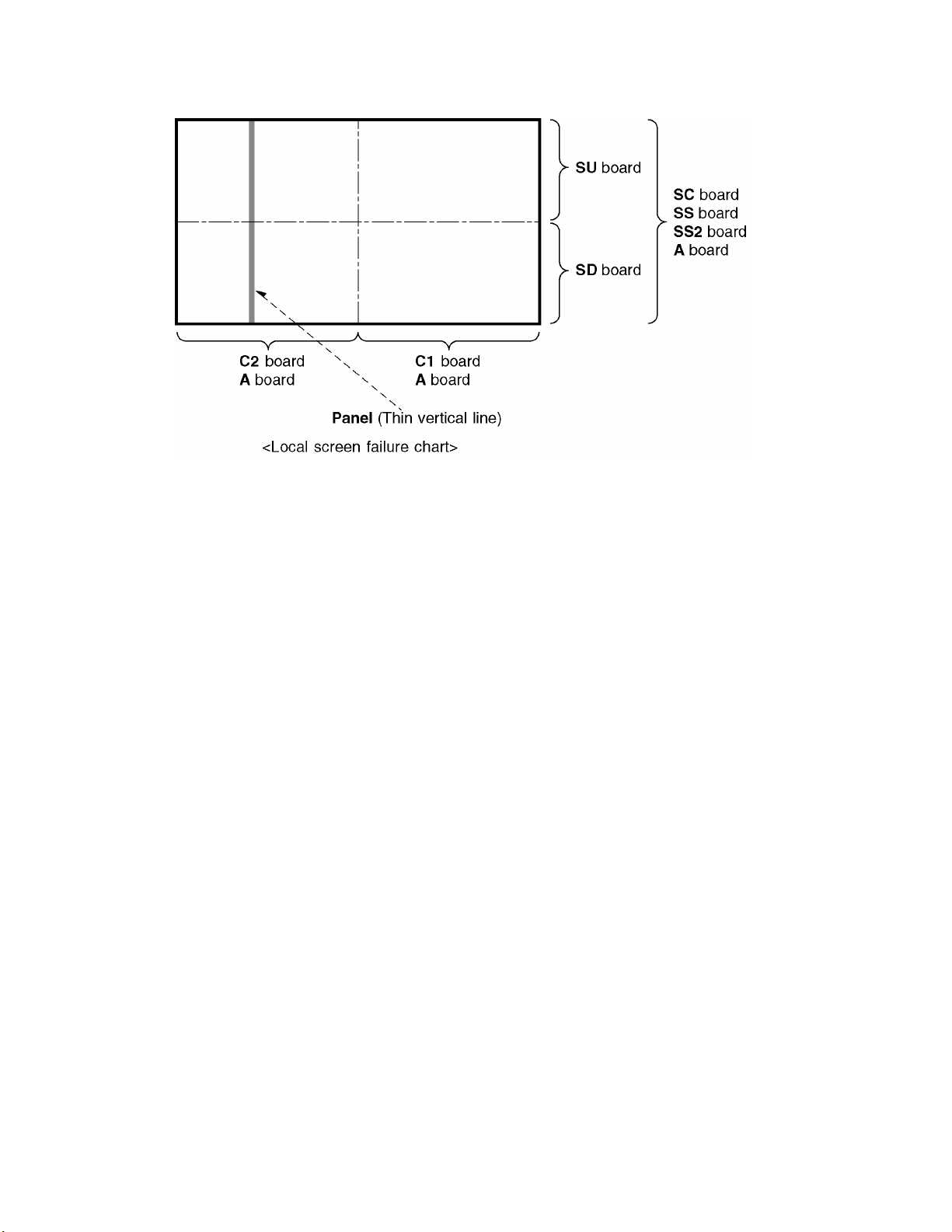
6.5. Local screen failure
Plasma display may have local area failure on the screen. Fig-1 is the possible defect P.C.B. for each local area.
Fig-1
16
Page 17

7 Disassembly and Assembly Instructions
7.1. Remove the Rear cover
1. See Service Hint (Section 3)
7.2. Remove the P-Board
Caution:
To remove P.C.B. wait 1 minute after power was off for discharge from electrolysis capacitors.
1. Unlock the cable clampers to free the cable
2. Disconnect the connectors (P2, P6, P7, P9, P11, P25 and
P35).
3. Remove the screws (×9 ) and remove the P-Board.
3. Remove the Adjustment cover.
4. Remove the screws (×4 , ×3 , ×1 ).
5. Remove the Rear terminal cover.
7.4. Remove the Tuner unit
1. Unlock the cable clampers to free the cable.
2. Disconnect the connectors (A1, A6 A11, A12 and A25).
3. Disconnect the flexible cables (A20, A31 and A32).
4. Remove the screws (×2 ) and remove the Tuner unit.
7.3. Remove the Side terminal
cover and Rear terminal cover
1. Remove the claw (×1 ).
2. Remove the Side terminal cover.
17
Page 18
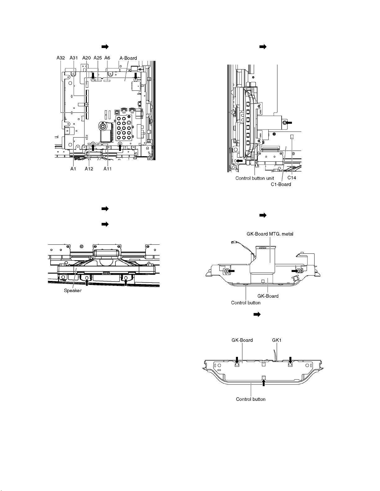
7.5. Remove the A-Board
1. Remove the Tuner unit. (See section 7.4.)
2. Remove the screws (×4 ) and remove the A-Board.
7.6. Remove the Speakers
1. Unlock the cable clampers to free the cable.
2. Disconnect the relay connector.
3. Remove the screws (×2 ) and remove the Speaker R.
4. Disconnect the connector (A12). (See section 7.4.)
5. Remove the screws (×2 ) and remove the Speaker L.
7.7. Remove the Control button unit
1. Disconnect the connector (C14).
2. Remove the screws (×2 ).
3. Remove the Control button unit.
7.8. Remove the GK-Board
1. Remove the Control button unit. (See Section 7.7.)
2. Remove the screws (×2 ).
3. Remove the GK-Board MTG. metal.
4. Remove the claw (×3 ).
5. Disconnect the connector (GK1).
6. Remove the GK-Board from Control button.
18
Page 19
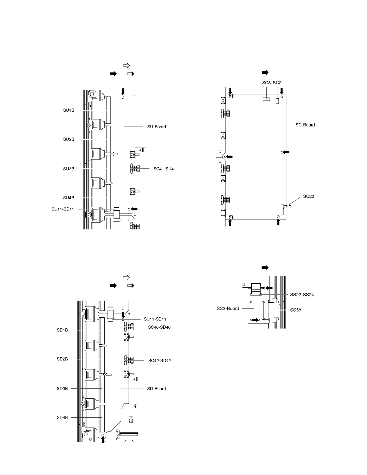
7.9. Remove the SU-Board
1. Remove the flexible cables (SU1B, SU2B, SU3B and
SU4B) connected to the SU-Board.
2. Remove the flexible cable (SU11-SD11) and the bridge
connector (SC41-SU41).
3. Remove the molding prop (×1 ).
4. Remove the screws (×2 , ×2 ) and remove the SU-
Board.
7.11. Remove the SC-Board
1. Remove the SU-Board and SD-Board. (See section 7.9.
and 7.10.)
2. Unlock the cable clampers to free the cable.
3. Disconnect the connectors (SC2 and SC3).
4. Disconnect the flexible cable (SC20).
5. Remove the screws (×6 ) and remove the SC-Board.
7.10. Remove the SD-Board
1. Remove the flexible cables (SD1B, SD2B, SD3B and
SD4B) connected to the SD-Board.
2. Remove the flexible cable (SU11-SD11) and the bridge
connectors (SC42-SD42 and SC46-SD46).
3. Remove the molding prop (×1 ).
4. Remove the screws (×2 , ×2 ) and remove the SD-
Board.
7.12. Remove the SS2-Board
1. Remove the Tuner unit. (See section 7.4.)
2. Disconnect the bridge connector (SS22-SS24) and disconnect the flexible cable (SS58).
3. Remove the screws (×2 ) and remove the SS2-Board.
19
Page 20
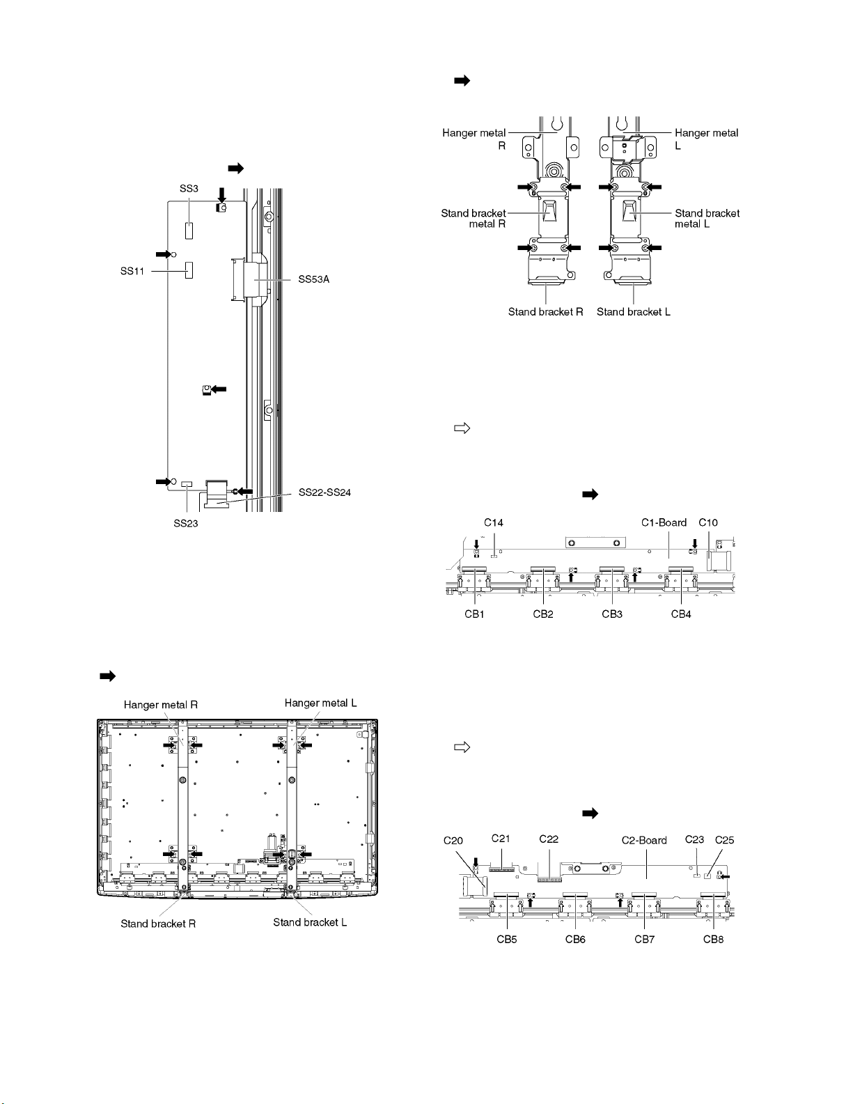
7.13. Remove the SS-Board
1. Remove the Tuner unit. (See section 7.4.)
2. Unlock the cable clampers to free the cable.
3. Disconnect the connectors (SS3, SS11 and SS23).
4. Disconnect the flexible cable (SS53A).
5. Disconnect the bridge connector (SS22-SS24).
6. Remove the screws (×5 ) and remove the SS-Board.
3. Remove the Stand brackets (L, R) fastening screws (×4
each) and remove the Stand bracket metals (L, R)
and the Stand brackets (L, R).
7.15. Remove the C1-Board
1. Remove the Control button unit. (See section 7.7.)
2. Remove the Hanger metal R and the Stand bracket R.
(See section 7.14.)
3. Remove the flexible cables holder fastening screws (×8
).
4. Disconnect the flexible cables (CB1, CB2, CB3 and CB4).
5. Disconnect the connector (C14).
6. Disconnect the flexible cable (C10).
7. Remove the screws (×4 ) and remove the C1-Board.
7.14. Remove the Hanger metals and
the Stand brackets
1. Remove the Plasma panel section from the servicing
stand and lay on a flat surface such as a table (covered
by a soft cloth) with the Plasma panel surface facing
downward.
2. Remove the Hanger metals (L, R) fastening screws (×4
each) and remove the Hanger metals (L, R).
7.16. Remove the C2-Board
1. Remove the Tuner unit. (See section 7.4.)
2. Remove the Hanger metal L and the Stand bracket L.
(See section 7.14.)
3. Remove the flexible cables holder fastening screws (×8
).
4. Disconnect the flexible cables (CB5, CB6, CB7 and CB8).
5. Disconnect the flexible cables (C20, C21 and C22).
6. Disconnect the connectors (C23 and C25).
7. Remove the screws (×4 ) and remove the C2-Board.
20
Page 21
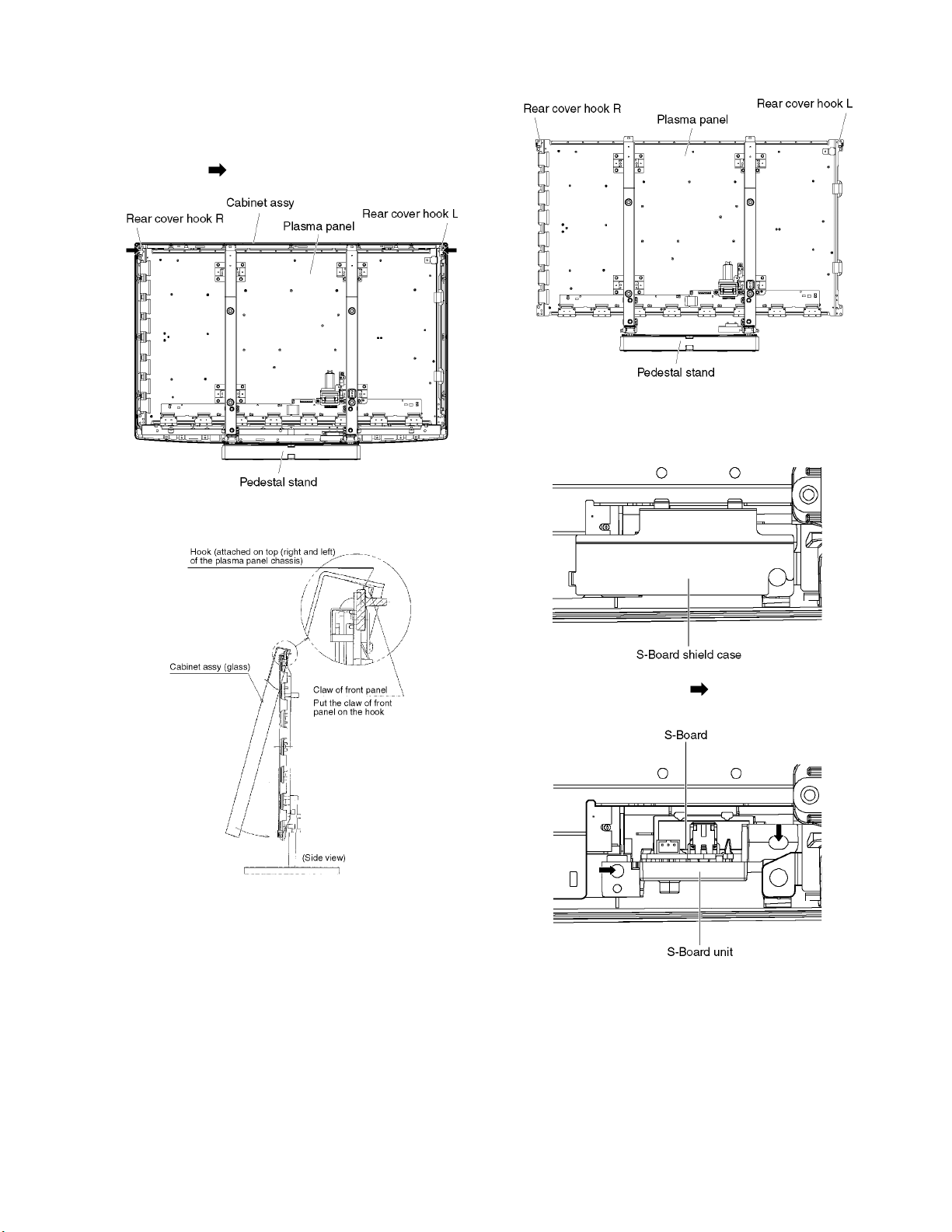
7.17. Remove the Plasma panel section from the Cabinet assy
(glass)
1. Remove the cabinet assy and the plasma panel fastening
screws (×2 ).
2. For leaving the plasma panel from the front frame, pull the
bottom of the cabinet assy forward, lift, and remove.
3. Remove the Rear cover hooks (L, R).
7.18. Remove the S-Board
1. Remove the Cabinet assy. (See section 7.17.)
2. Remove the S-Board shield case.
3. Remove the screws (×2 ) and remove the S-Board
unit.
21
Page 22
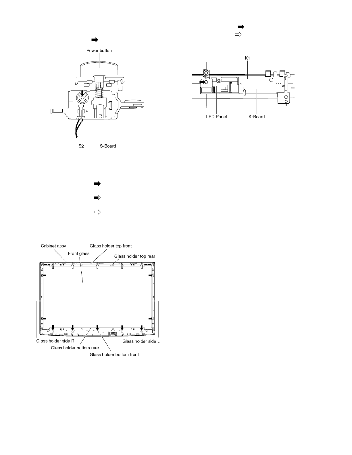
4. Disconnect the connector (S2).
5. Remove the Power Button.
6. Remove the screw (×1 ) and remove the S-Board.
7.19. Remove the K-Board
1. Remove the Cabinet assy. (See section 7.17.)
2. Remove the S-Board. (See section 7.18.)
3. Remove the screws (×5 ).
4. Remove the Glass holder bottom rear.
5. Remove the screws (×4 ).
6. Remove the Glass holder side (L, R).
7. Remove the screws (×7 ).
8. Remove the Glass holder top rear and the Glass holder
top front.
9. Remove the Glass holder bottom front.
10. Remove the screw (×1 ).
11. Remove the claw (×1 ).
12. Disconnect the connector (K1) and Remove the K-Board
from LED Panel.
7.20. Replace the plasma panel
1. Place the new plasma panel on the flat surface of the
table (covered by a soft cloth), with the plasma panel surface facing downward.
2. Attach the C1-Board and the C2-Board, connect the flexible cables (×8) from the plasma panel to the C1-Board
and the C2-Board, and fit the flexible cable holders.
3. Attach the Hooks (left, right) and fit the Stand brackets (L,
R) to the new plasma panel.
4. Place the plasma panel section on the servicing stand.
5. Attach the cabinet assy and each P.C.Board and so on, to
the new plasma panel.
*When fitting the cabinet assy, be careful not to allow
any debris, dust or handling residue to remain
between the front glass and plasma panel.
22
Page 23
8 Measurements and Adjustments
8.1. Adjustment Procedure
8.1.1. Driver Set-up
8.1.1.1. Item / Preparation
1. Input a white signal to plasma video input.
2. Set the picture controls as follows.
Picture menu: Vivid
Normal: Set
Aspect: Full
Caution
1. First perform Vsus adjustment.
2. The Vscn voltages are measured from the Vad (Vad_base), but may be measured from the GND (GND_base) in an
unavoidable case.
8.1.1.2. Adjustments
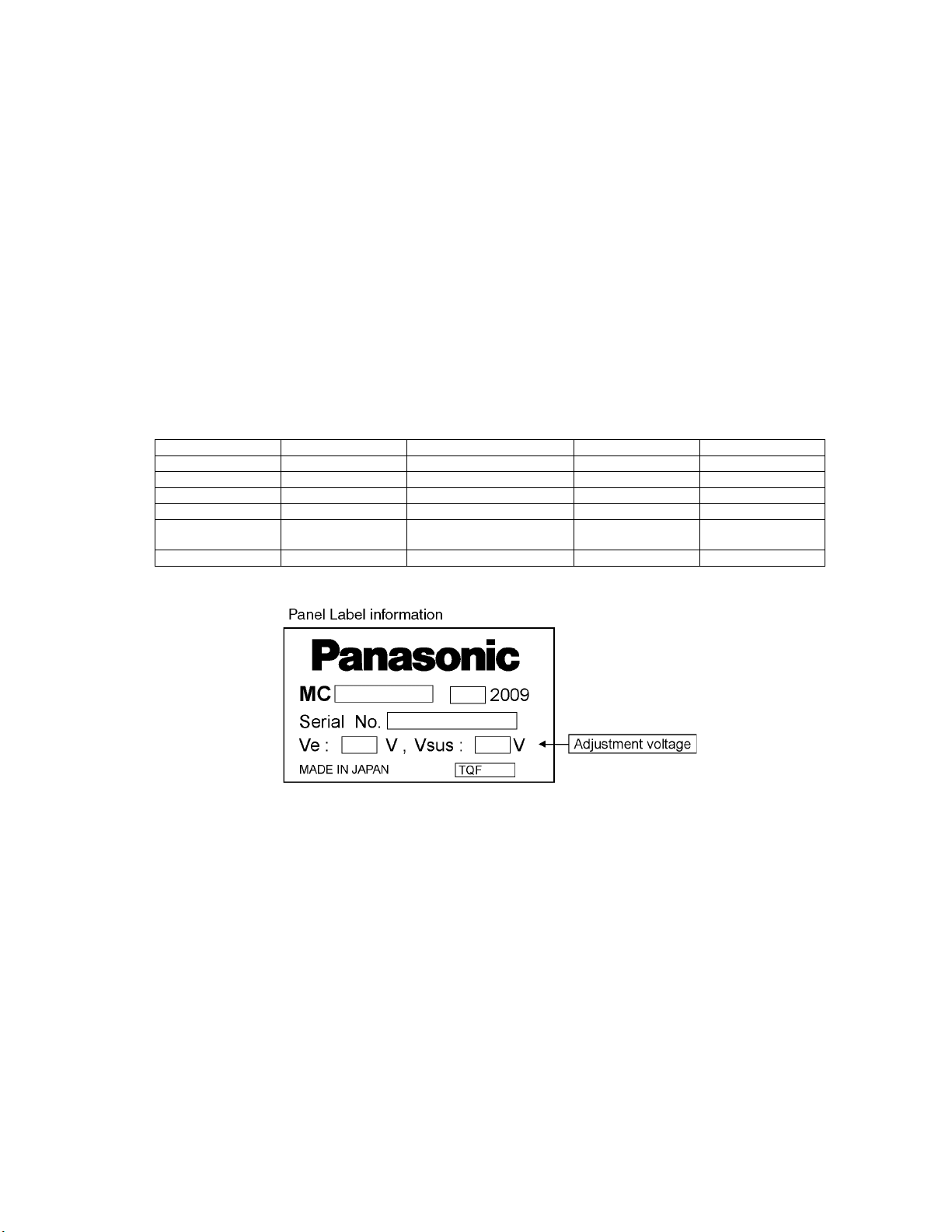
Adjust driver section voltages referring the panel data on the panel data label.
Check or adjust the following voltages with the multimeter.
Name Test Point Voltage Volume Remarks
Vsus TPVSUS (SS) Vsus ± 2V R737 (P) *
Ve TPVE (SS) Ve ± 2.5V Fixed *
Vset TPVSET (SC) 290V ± 9V Fixed
Vad TPVAD (SC) -180V ± 2V VR16600 (SC)
Vscn TPVSCN (SC) Vad_base : 145V ± 4V
GND_base : - 35V ± 6V
Vda TPVDA (P) 60V + 1V, - 2V Fixed
Fixed
*See the Panel label.
23
Page 24

8.1.2. Initialization Pulse Adjust
1. Input the White signal to plasma video input.
2. Set the picture controls as follows.
Picture menu : Vivid
Normal : Set
Aspect : Full
3. Connect Oscilloscope to TPSC1 (SC).
Check the voltage (T2) at 100μs period on the down slop.
Test point Volume Level
T2 TPSC1 (SC) VR16601 (SC) 210 V ± 10 V
8.1.3. P.C.B. (Printed Circuit Board) exchange
8.1.3.1. Caution
1. To remove P.C.B., wait 1 minute after power was off for discharge from electrolysis capacitors.
8.1.3.2. Quick adjustment after P.C.B. exchange
Adjust the following voltages with the multimeter.
P.C.B. Name Test Point Voltage Volume Remarks
P Board Vsus TPVSUS (SS) Vsus ± 2V R737 (P) *
SC Board Vad TPVAD (SC) -180V ± 2V VR16600 (SC)
A Board White balance and Sub brightness for NTSC, PAL, HD, PC and 625i signals
*See the Panel label.
Caution:
Absolutely do not reduce Vsus below Ve not to damage the P.C.B.
24
Page 25
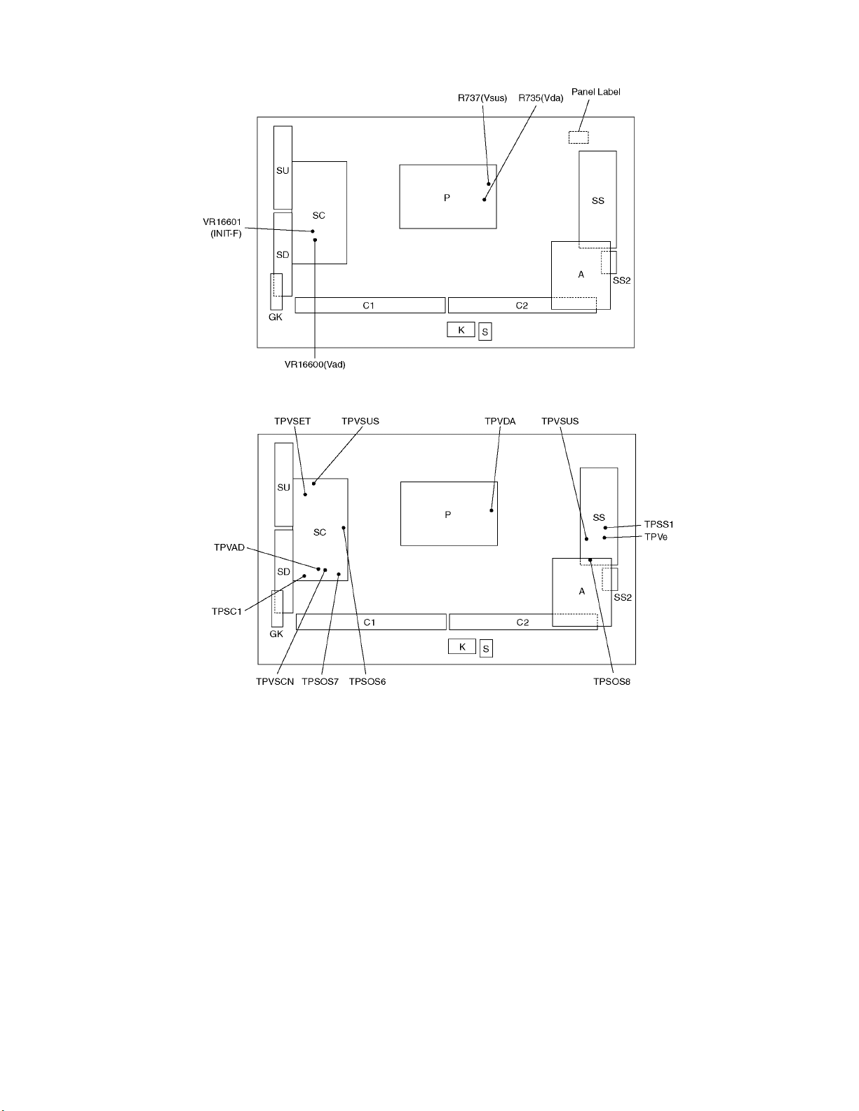
8.1.4. Adjustment Volume Location
8.1.5. Test Point Location
25
Page 26
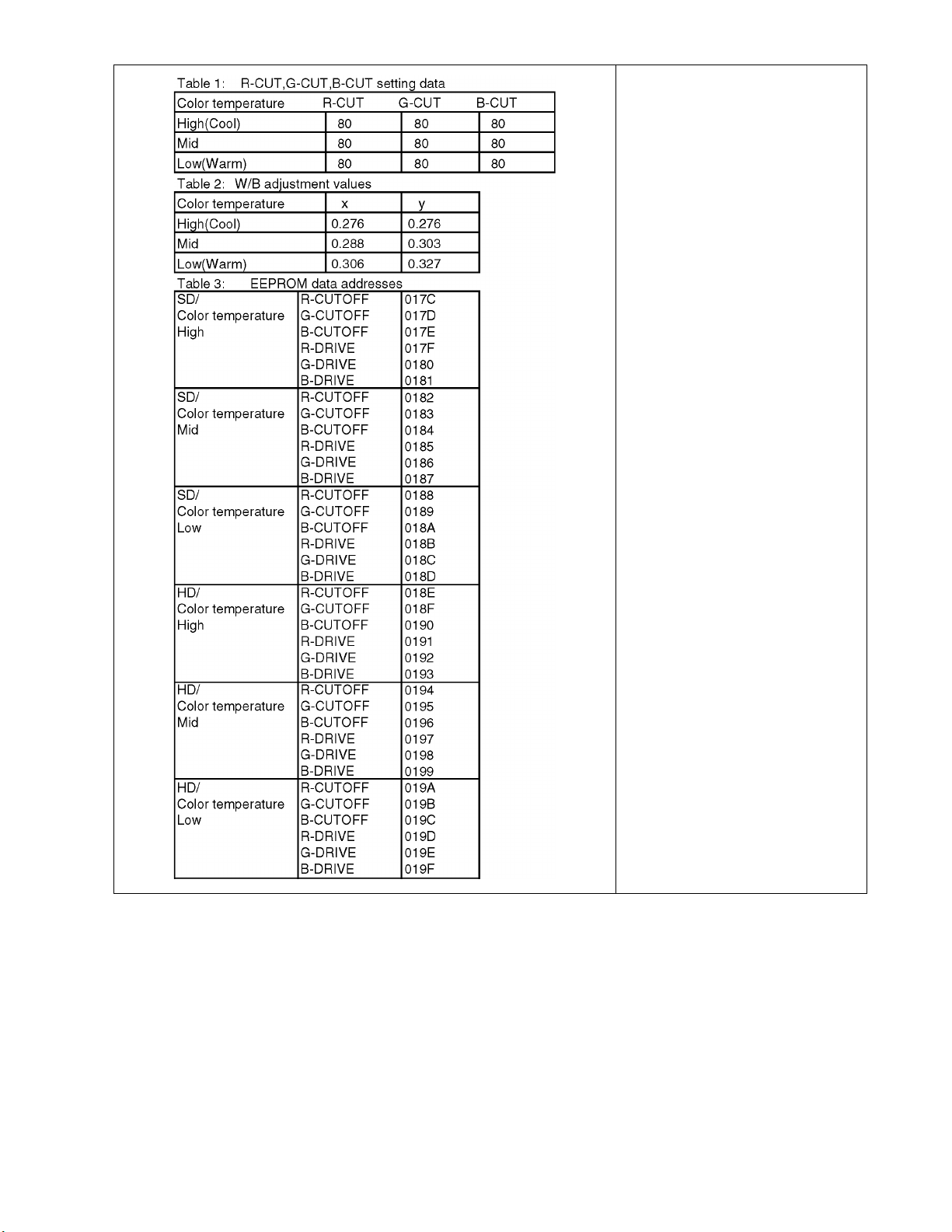
8.2. Adjustment
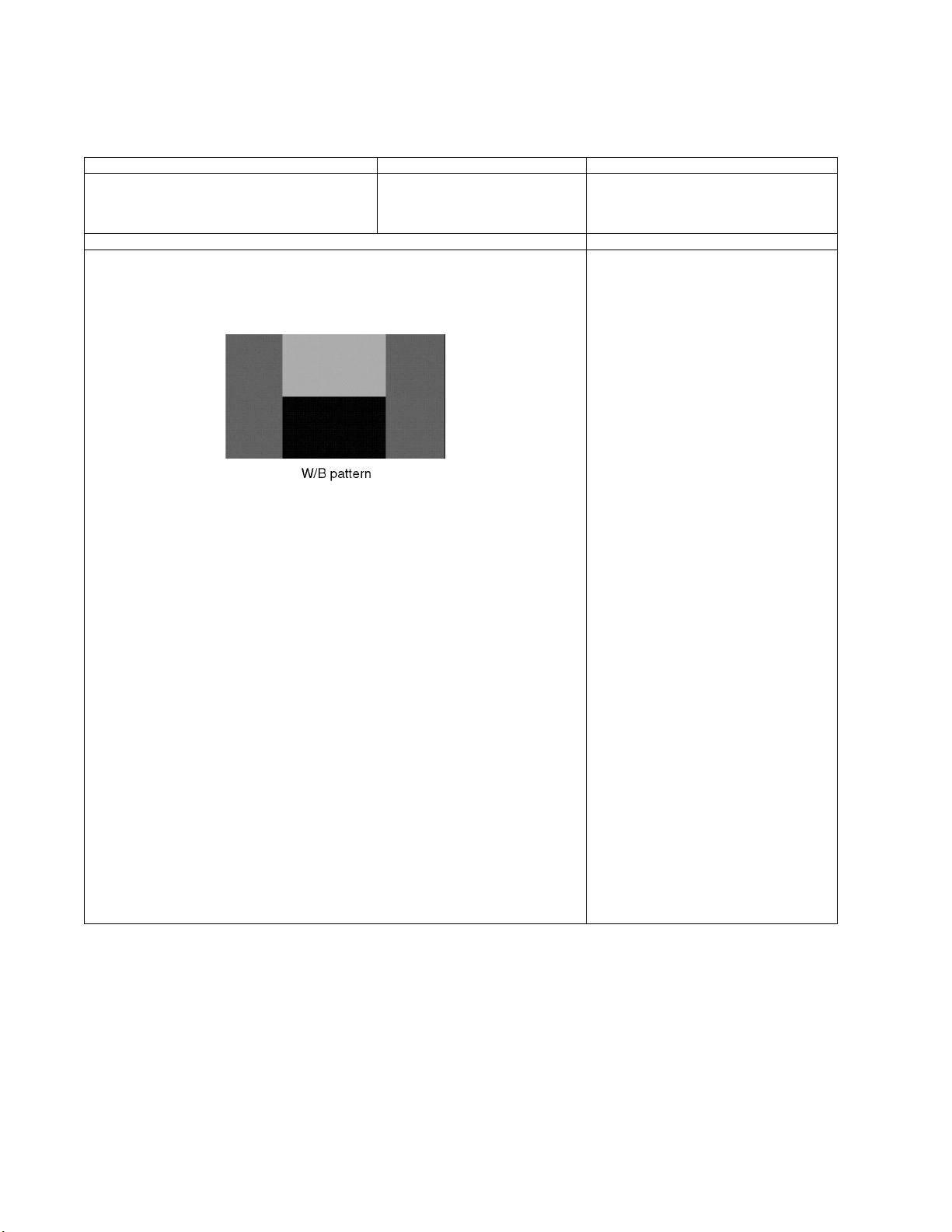
8.2.1. White balance adjustment
Name of measuring instrument Connection Remarks
• W/B pattern
• Color analyzer
(Minolta CA-100 or equivalent)
Procedure Remarks
• Make sure the front panel to be used on the final set is fitted.
• Make sure a color signal is not being shown before adjustment.
• Put the color analyzer where there is little color variation.
1. Set the Picture menu to [vivid] and output the W/B pattern.
2. Check that the color temperature is [Cool].
3. Set to serviceman mode, WB-ADJ.
4. Set [R-CUT] [G-CUT] [B-CUT] the values written in table 1.
5. Attach the sensor of color analyzer to the center of highlight window.
6. Fix G drive at C0h and adjust [B-DRV] and [R-DRV] so x, y value of color analyzer
become the [Color temperature High] in table 2.
7. Increase RGB together so the maximum drive value in RGB becomes FC. That is,
set [ALL DRIVE] to FC.
Execute adjustment again. When that, the maximum value of R/G/B DRV should be FC,
and either R/G/B DRV should be FC.
8. Set color temperature to [Normal].
9. Set [R-CUT] [G-CUT] [B-CUT] the values written in table 1.
10. Attach the sensor of color analyzer to the center of highlight window.
11. Fix G drive at C0h and adjust [B-DRV] and [R-DRV] so x, y value of color analyzer
become the [Color temperature Mid] in table 2.
12. Increase RGB together so the maximum drive value in RGB becomes FC. That is,
set [ALL DRIVE] to FC.
Execute adjustment again. When that, the maximum value of R/G/B DRV should be FC,
and either R/G/B DRV should be FC.
13. Set color temperature to [Warm].
14. Set [R-CUT] [G-CUT] [B-CUT] the values written in table 1.
15. Attach the sensor of color analyzer to the center of highlight window.
16. Fix G drive at C0h and adjust [B-DRV] and [R-DRV] so x, y value of color analyzer
become the [Color temperature Low] in table 2.
17. Increase RGB together so the maximum drive value in RGB becomes FC. That is,
set [ALL DRIVE] to FC.
Execute adjustment again. When that, the maximum value of R/G/B DRV should be FC,
and either R/G/B DRV should be FC.
18. Set color temperature to [Cool].
Component input
or HDMI input
or ATSC 1080i signal
Panel surface
26
Page 27
27
Page 28

28
Page 29

COLD
(LED:4TIME)
(LED:7TIMES)
(LED:6TIMES)
HOT
(LED:8TIME)
(LED:6TIMES)
(LED:8TIMES)
(LED:10TIMES)
(LED:5TIMES)
(LED:2TIMES)
(LED:3TIMES)
(LED:4TIMES)
(LED:10TIMES)
(LED:7TIMES)
F15V
AC CORD
SU11
SUSTAIN
VOLTAGE
RECTIFIER
+5V(P)
POWER MICOM
SCAN
DRIVER
VSUS GEN.
SS2
SUSTAIN CONTROL
+15V(P)
STB5V
+15V(P)
(LOWER)
SOS8_SS
VSUS
SS-BOARD
SOS DETECT
SC41
SCAN OUT (UPPER)
SD11
CONNECTOR
VSUS
Vda
SU41
P6
RECTIFIER
P2
+5V(P)
POWER
FACTOR
CONTROL
SUSTAIN
+5V(P)
MAIN SW2
SC46
P-BOARD
SOS DETECT
VSET GEN.
VSUS
POWER SUPPLY
RELAY
P7
SS
PS SOS4
MAIN SW1
SC-BOARD
FLOTING PART
SOS DETECT
Vda
SCAN OUT (LOWER)
VIDEO DATA
VSUS
VE GEN.
SD
KEYSCAN1
SC2
SD42
SS24
SCAN DRIVE
CONTROL
PULSE
P
ENERGY RECOVERY
SC
F15V
BUFFER
SC-BOARD
ENEGRY RECOVERY
SOS DETECT
SS22
RECTIFIER
+5V(P)
SC42
P25
STANBY
VOLTAGE
RECTIFIER
SOS7_SC2
STB5V
SUSTAIN DRIVE
SCAN CONTROL
SC20
VSUS
+15V(P)
SU
SOS6_SC1
SS23
+15V(P)
PROCESS
VOLTAGE
RECTIFIER
ON/OFF CONTROL
SS11
SOUND15V
P11
+5V(P)
P35
P9
VIDEO DATA
VSCAN GEN.
VAD GEN.
SOS8_SS
P34
SUSTAIN CONTROL
+15V(P)
SCAN
DRIVER
+5V(P)
SD46
GK
KEY SWITCH
C21
DATA
DRIVER
DATA DRIVER (RIGHT)
SOS8_SS
+5V(P)
C23
DATA
DRIVER
+5V(P)
VIDEO DATA
SUSTAIN CONTROL
KEYSCAN1
DATA
DRIVER
C2
SOS8_SS
DATA DRIVER (LEFT)
DATA
DRIVER
Vda
C10
DATA
DRIVER
+5V(P)
C22
C1
DATA
DRIVER
DATA
DRIVER
C14
Vda
GK1
Vda
C20
DATA
DRIVER
C25
SUSTAIN CONTROL
KEYSCAN1
KEY SWITCH
+5V(P)
VIDEO DATA
POWER
OPTICAL
K1
A11
SUB9V
HDMI DATA
+3.3V(STB)
AUDIO SW
KEYSCAN1
+5V(P)
R
+5V(P)
DCDC
(SIDE)
EEPROM
SUB5V
VIDEO SW
SOS6_SC1
DCDC
HDMI DATA
KEYSCAN3
PAMEL SOS
PANEL MICOM
TUNER SOS
+5V(P)
PANEL STB_ON
L,R
OPTICAL AUDIO OUT
SD CARD DATA
HDMI SW
AMP
LVDS DATA
LVDS DATA
VIDEO DATA
PD2-M
STB3.3V
SOS7_SC2
BT30V
BT30V
DDR2
SUB+9V DET
SUSTAIN
CONTROL
REMOTE IN
SOS8_SS
IIC1
VIDEO DATA
TUNER SOS DET
CIRCUIT
DCDC
RESET
DCDC
K
FLASH
PLASMA AI
CPG with SS
H/V Sync Control
Sub Filed Processor
Plasma AI
+15V(P)
+15V(P)
+1.8V(P)
SUB1.3V
SOS8_SS
F15V
A6
PANEL STATUS
BT30V
ON
+5V(S)
+3.3V(S)
PANEL STB_ON
+3.3V(P)
C.A.T.S. SENSOR
+15V(P) DET
PANEL STATUS
SUB5V
A20
SOS6_SC1
RESET
SUB9V
F15V
+2.5V(P)
A25
A31
+5V(P)
+15V(P)
L,R
+2.5V(P)
STB3.3V
REMOTE RECEIVER
SUB1.8V
V
SOS7_SC2
SUB+5V DET
A32
SD0
EEPROM
DDR
STB5V
COMP2
PANEL
MAIN ON
MEMORY
TMDS DATA
POWER SOS
POWER LED
TUNER
Y,PB,PR
STB5V
SUB9V
POWER SWITCH
LED(R)
L,R
DCDC
R,G,B
TUNER SOS
+3.3V(P)
A1
L,R
SUB1.3V
SUB+3.3V DET
F15V
OPTICAL OUT
STB_D3.3V
+3.3V(P) DET
+1.8V(P)
SYSTEM MPU
COMP1
+3.3V(P)
AUDIO
SUB9V
SUB3.3V
SOUND
+15V(P)
SUB3.3V
L,R
Y,PB,PR
L
A12
SD CARD DATA
SWITCH
A/D
+1.2V(P)
IFD_OUT
STB5V_M
PAMEL SOS
SUB5V
S2
DCDC
SCAN CONTROL
HDMI2
STB_D3.3V
L,R
SBO2
SBI2
SLOT
+5V(P)
DCDC
A
+5V(P)
OUT
KEYSCAN1
SD
Seine3LV
VIDEO2
+9V(S)
+3.3V(STB)
VSB_IN
SD
V,Y,C
HDMI1
SPEAKER(L)
SPEAKER(R)
SUB1.8V
POWER LED(R)
DISCHARGE
CONTROL
VIDEO1
+5V(P) DET
R,G,B
DCDC
SD CARD
C.A.T.S. SENSOR
SOUND15V
SDIN
AUDIO
S
+1.2V(P)
DIGITAL SIGNAL PROCESSOR
V
CONTROL
SIGNAL
SUB5V
TMDS DATA
REMOTE RECEIVER
C.A.T.S. SENSOR
COLD
(LED:4TIME)
(LED:7TIMES)
(LED:6TIMES)
HOT
(LED:8TIME)
(LED:6TIMES)
(LED:8TIMES)
(LED:10TIMES)
(LED:5TIMES)
(LED:2TIMES)
(LED:3TIMES)
(LED:4TIMES)
(LED:10TIMES)
(LED:7TIMES)
9 Block Diagram
9.1. Main Block Diagram
29
Page 30
9.2. Block (1/3) Diagram
(LED:10TIMES)
JK3000
JK3701
VIDEO2
(SIDE)
VIDEO1
COMP1
COMP2
ANT IN
D3005
OPTICAL
AUDIO
JK8302
SD CARD
P6
P7
STB5V
TV SUB ON
14 291
13
A6
PA5600
STB5V
SUB9V
SUB5V
IIC1
SOUND15V
A12
L(+)
1
L(-)
2
A11
R(+)
1
R(-)
3
F15V
F15V
F15V
SOUND15V
SOUND15V
SOUND15V
8
3
7
SUB5V
SUB9V
SUB3.3V
LVDS DATA
STB3.3V
SPEAKER_L
SPEAKER_R
1
2
3
4
5
6
RX1
RX2
SUB9V
SUB1.3V
JK4500 JK4501
HDMI IN 1
TMDS DATA
CLOCK
DDC IIC
Q4530
+5V
HDMI_CEC
DET_1
+5V(HDMI)
HDMI IN 2
TMDS DATA
IC5401
+9V
SUB5V
IC5607
SUB3.3V
+5V
+3.3V
SUB1.8V
IC5608
SUB1.3V
+1.8V
+1.3V
CLOCK
DDC IIC
Q4529
+5V
HDMI_CEC
DET_2
+5V(HDMI)
Q5603
ON/OFF
Q5604
F15V DET
D5692
HDMI_CEC
F15V
TV SUB ON
TUNER SOS
(LED:10TIMES)
STB_RESET
KEYSCAN3
DTV RESET
IC5606
STB
RESET
D5613
Q5522
VOLTAGE
DROP
ERROR DET
F15V
D5521
SUB9V
SUB5V
BT30V
BT30V
L5441
D5485
D5486
D5614D5615
D5484
SOUND15V
D5522
STB3.3V
IIC0
IIC1_
EEP
STB5V
SDIN
L5442
F15V
BT30V
SUB9V
SUB5V
STB3.3V
STB_RESET
ANALOG ASIC
IC2109
AUDIO AMP
+15V
SYS_IIC0
IC5480
DTV5V
DRV
STB
+3.3V
MUTE
SPEAKER
L_OUT
SPEAKER
R_OUT
DIGITAL SIGNAL PROCESSOR
A
V2_V
V2_L
V2_R
STB5V
IC4500
EEPROM
IC8003
0.9V
IC4503
HDMI SW
3.3V
EEPROM
DDC1_IIC
DDC2_IIC
DDC_IIC
SUB5V
SUB1.8V
IC4501
IC3001
V1_Y
V1_C
V1_V
V1_L
V1_R
D1_Y
D1_PB
D1_PR
D1_L
D1_R
D2_Y
D2_PB
D2_PR
D2_L
D2_R
TU8300
TUNER
SYS_IIC2_TU
V1
V2 V2
D1
D2
TV_V
VIDEO
TV_L
TV_R
AUDIO
AFT
BT30V
BT30V
SUB5V
5V
IFD_OUT1
IFD_OUT2
IF_AGC
OPTICAL AUDIO OUT
OUT
SD DATA:4bit
VIDEO SW
TV
TV
V
VIDEO1
Y/C/V
VIDEO2
V L/R
VIDEO3
VIDEO4
COMP1
Y/PB/PR
COMP2
Y/PB/PR
PC
R/G/B/H/V
DTV1
Y/C
DTV2
Y/C
TV_VIDEO
AFT
VINP_VSB
VINN_VSB
IIC0
DDC_
IIC
SBI2
SBO2
SUB3.3V
IC8001
+5V(HDMI)DET 1,2
+5V(HDMI)
DET 1,2
VSB_I/F
IF_AGC
SPDIF
SD CARD
I/F
TV
V1
D1
D2
SUB9V
Seine3LV
AUDIO SW
AUDIO
I/F
CLOCK
RESET
IIC_IF
MAIN
OUT
MAIN L/R
RGB_CVBS
Y/PB/PR
PC_HS/VS
OUT
SUB MONO
L+R
HDMI_3.3V
3.3V
SUB2.5V
2.5V
3.3V
1.8V
1.3V
HS/VS
SDO
SDIN
R/G/B
HDMI DATA
LVDS DATA
L/R
R/G/B
HS/VS
HS/VS
SUB
OUT
HDMI DATA
SUB3.3V
IC8008
3.3V
IC8007
2.5V
IC2107
SOUND A/D
L/R
IC8009
IC8002
CLK BUFFER
DDR2
IC8004
CLOCK GEN
IC8502
NOR FLASH
RESET
EEPROM
IC8503
IIC1_
EEP
TV
L/R
VIDEO1
L/R
VIDEO2
VIDEO3
L/R
VIDEO4
L/R
COMP1
L/R
COMP2
L/R
PC
L/R
DTV1
L/R
5V9V
SYS_IIC0
PC_HS/VS
R/G/B_IN
HDMI_IN
LVDS_OUT
DDR I/F
DDRVREF
CPU BUS
I/F
30
Page 31

9.3. Block (2/3) Diagram
(LED:10TIMES)
(LED:2TIMES)
(LED:4TIMES)
(LED:7TIMES)
(LED:6TIMES)
(LED:5TIMES)
(LED:3TIMES)
(LED:8TIMES)
1
2
3
4
5
6
SUB5V
SUB9V
SUB3.3V
LVDS DATA
STB3.3V
STB3.3V
HDMI_CEC
TV SUB ON
TUNER SOS
AFT
DTV RESET
STB RESET
TV_VIDEO
IC1101
EEPROM
IC4800
TEMP SENSOR
Q1105
IC1102
IIC1_
EEP
SYS_
IIC2_TU
AND
DIGITAL SIGNAL PROCESSOR
A
IC9900
*PLASMA AI
*CPG with SS
*H/V Sync Control
*Sub Filed Processor
*Plasma AI
FLASH I/F
DDR I/F
+3.3V
RESET
IC9807
+2.5V
PD2-M
3.3V
STB_D3.3V
A31
C21
SW2500
POWER SWITCH
14
VIDEO DATA
57
1
+5V(P)
2
+5V(P)
5
+3.3V(P)
CONTROL DATA
4
KEYSCAN1
A32
C22
6
VIDEO DATA
58
CONTROL DATA
2
+5V(P)
1
+5V(P)
SUSTAIN CONTROL
68
SOS8_SS
SC20
A20
SCAN CONTROL
17
UHZ
14
SOS6_SC1
15
SOS7_SC2
29
+15V(P)
30
+15V(P)
1
+5V(P)
P25
A25
11
PANEL_MAIN_ON
12
SOS4_PS
5
+5V(P)
6
+5V(P)
1
+15V(P)
2
+15V(P)
9
STB5V
VIDEO DATA
VIDEO DATA
Config(CCLK,DDTATA,PROGB),
FPCLK,FPDATA[1:0],FVSEL
2.5V
1.2V
OSD I/F
IC9003
PANEL MICOM
OSD I/F
IIC2
IIC2
IIC1
IIC1
STB_D3.3V
RESET
POWER ON/OFF
PANEL SOS
PANEL STATUS
+3.3V(P) DET
(LED:3TIMES)
P1.2V
EEPROM
P3.3V
IC9001
STB3.3V
SUB5V
DRVRST
FPGARST
XRST
XRST,
XRSTSYS
IC9500
DISCHARGE CONTROL
3.3V
1.2V
CONTROL DATA
SUSTAIN CONTROL
SCAN CONTROL
GenX7
PANEL MAIN ON
IC9805
+3.3V
IC9806
+1.2V
A1
R_LED_ON
C.A.T.S.
2
REMOTE IN
5
STB+3.3V
3
SUB+5V
1
KEYSCAN3
FOR
FACTORY
A17
USE
FOR
FACTORY
A18
USE
Config(DONE)
Config(DONE)
SOS8_SS
(LED:8TIMES)
(LED:6TIMES)
SOS6_SC1
SOS7_SC2
(LED:7TIMES)
AUX_ON/OFF
POWER SOS
(LED:4TIMES)
+5V(P) DET
(LED:5TIMES)
+15V(P) DET
(LED:2TIMES)
IIC2
2.5V
UHZ
K1
10
9
+2.5V
PC2501
C.A.T.S.
SENSOR
RM2501
REMOTE
RECEIVER
KEYSCAN3
IC9808
P5V
S2
2
1
S
IIC3
P15V
D2520
K1
POWER LED
66
2
5
3
1
88
K
POWER LED POWER SWITCH
REMOTE RECEIVER
C.A.T.S. SENSOR
ON
IIC2
LVDS DATA
IC9303
P3.3V
P2.5V
FLASH
MEMORY
IC9901
ADDR/DATA
DDR
P2.5V
IC9004
STB+3.3V/RESET
HDMI_CEC_
OUT
HDMI_CEC_
PU_ON
IC1100
SYSTEM MPU
TV SUB ON
TUNER SOS
(LED:10TIMES)
AFT
DTV RESET
STB RESET
TV_VIDEO
STB3.3V
SYS_
IIC0
IIC0
IIC1
IIC2
SUB5V DET
SUB9V DET
SUB3.3V DET
IIC0
PANEL STB_ON
PANEL SOS
PANEL STATUS
KEYSCAN1
POWER LED(R)
C.A.T.S. SENSOR
REMOTE IN
KEYSCAN3
SBI2
SBO2
PANEL STB_ON
PANEL SOS
PANEL STATUS
KEYSCAN3
STB5V_M
PANEL STB_ON
PANEL SOS
PANEL STATUS
31
Page 32

9.4. Block (3/3) Diagram
(LED:7TIMES)
(LED:6TIMES)
(LED:8TIMES)
COLD
(LED:4TIMES)
HOT
COLDHOT
SUSTAIN DRIVE
SS
SS
P11
11
1
Vsus
4
+15V(P)
SOS8_SS
SUSTAIN CONTROL
POWER SUPPLYP
T100
PFC
IC100
PFC
CONTROL
D100
RECTIFIER
LIVE
NEUTRAL
T630mAL 250V
F200
F201
L100,L101
FILTER
T8AH 250V
NEUTRAL
SC35SS3
MID
MID
C23
+5V(P)
Q104
PFC
R141
3
SS
23
1
5
COMPARATOR
D200
RECTIFIER
LIVE
1
2
AC CORD
SUSTAIN CONTROL
PR101
IC301
Q302,Q303
POWER
CONTROL
D302
IC300
IC200
AC DET
F100F101
T8AH 250V
P9
IC16131
VSUS Gen.
DRIVER
IC16241
BUFFER
Q304,Q305
RESONANCE
UMH
UML
MID
IC303
PHOTO COUPLER
IC304
PHOTO COUPLER
IC302
PHOTO COUPLER
IC601
PHOTO COUPLER
IC600
PHOTO COUPLER
IC201
STB
CONTROL
TPVSUS
UMH
UML
UEH
T301
T300
RL102
RL101
RL100
T200
D204
COLDHOT
PHOTO
COUPLER
HOT
Q16001,2
Q16021,2
D706
D700
D705
Q600
Q602
IC202
FPC DET
Q609
D502
COLD
D501
D506
VE GEN.
PHOTO
COUPLER
PC16191
VE Gen.
DRIVER
D16280
(LED:8TIMES)
Vsus
ERROR DET
IC500
STB
ERROR DET
IPD CIRCUIT
IC16304
PC16192
IC16312
SHUNT
REG.
UEH
ERROR DET
IC700
PFC_ON/OFF
MAIN SW_ON
MAIN RELAY_ON
RUSH RELAY_ON
AC DET
TPSS1
Q16280
+5V
TPVE
Q16101
Q16102
Vsus
R737
IC603
POWER MICOM
IC602
RESET
P34
IC502
D16282
+15V
Vda
ERROR DET
RESET
F_15_ON
13
SS
53A
1
2
13
SS
22
15
1
14
IC701
POWER SOS
(LED:4TIMES)
POWER SOS
PANEL_MAIN_ON
ALL_OFF
TV SUB ON
Q505
P6
A6
SS
24
15
14
SS2
STB5V_
ON/OFF
7
1
FSTB+15V
PLASMA PANEL
PANEL SUSTAIN
ELECTRODE
SS
1
58
SUSTAIN
CONNECTOR
(LOWER)
Vda
R735
FSTB+15V
+15V(SND)
3
1
9
FSTB+15V
+15V(SND)
+15V(SND)
KEYSCAN1
+5V(P)
67
68
BUFFER
CONTROL DATA
+5V(P)
46
VIDEO DATA
28
30
12
C22
CB6
A32
DATA DRIVER (RIGHT)
GK KEY SWITCH
GK1
KEY SWITCH
2
13
1
KEYSCAN1
C14
1
CB1
C1
BUFFER
IC17103,04
CB2
C10
KEYSCAN1
51 5
+5V(P)
55
IC17101,02
CB3 CB5
BUFFER
CB4
54
CONTROL DATA
VIDEO DATA
VIDEO DATA
4
1
+5V(P)
Vda
Vda
A31
65 6768
C21
C20
1
2
52
IC17211,12
55
VIDEO DATA
PANEL DRIVER PLASMA PANEL
SCAN DRIVE
SC
D711
D712
Q504
P7
A6
IC702
15V
Q704
OVER
VOLTAGE
DET
+5V(STB)
+5V(P)
1
Vsus
Vda
2
+15V(P)
+15V(P)
10
+15V(P)
5
+5V(P)
6
8
+5V(STB)
TV SUB ON
ALL_OFF
P2
1
P11
1
Vsus
4
+15V(P)
P35
1
Vda
2
Vda
P25
1
+15V(P)
2
+15V(P)
5
+5V(P)
6
+5V(P)
9
+5V(STB)
12
SOS4_PS
PANEL_
11
MAIN_ON
SCAN CONTROL
SS11
C25
A25
SOS6_SC1
SOS7_SC2
SC2
Vsus
1
IC16791
DC/DC
CONVERTER
IC16771
+5V
PC16461
PHOTO COUPLER
IC16464,65
INVERTER
IC16773
INVERTER
IC16501
CSH/CMH GATE
DRIVE CIRCUIT
IC16521
SCAN
CONTROL
VOLTAGE
DROP
ERROR DET
MAIN_STOP
VSCN
15V_F
CSL/CML GATE
DRIVE CIRCUIT
MID
IC16581
ERROR DET
TPSOS6
(LED:6TIMES)
TPSOS7
(LED:7TIMES)
SS3
A20
+15V(P)
+15V(P)
+5V(P)
SC3
3
MID
5
MID
SC
20
2
1
30
17
16
14
UHZ
16V-F
CMH
CSH
CSL
CML
NOR GATE
IC16563
D16480
D16820
TPVSUS
Q16401
Q16402
Q16441
D16583
LED(G)
PHOTO COUPLER
ERROR DET
PHOTO COUPLER
PHOTO COUPLER
PHOTO COUPLER
D16461
D16481
IC16561,62
BUFFER
D16493
UHZ
PC16480
Q16876
PC16601
PC16603
PC16684
Q16451
Q16421
Q16422
PC16685
PHOTO
COUPLER
D16920
Q16604
CPH2
Q16607
CERS
CPH1
Q16601
VOH
CIS
Q16621
Q16622
VOL
CPH1
CRC1
CML
CMH
CRC2
CPH2
CEL
CSH CIS OC2
CERS
CSL
IC16490,91
Q16490
SEPA PROTECT
CIRCUIT
D16473
D16791
D16821
D16871
TPVSET
SIU
OC1
CLK
CERS
15V_F
SCNR_PRO
Vscn
D16721
(15V_F)
IC16788,89
IC16661
COMPARATOR
IPD CIRCUIT
IC16786,87
IPD CIRCUIT
VSCN GEN.
SHUNT REG
IC16724
+5V
(SC1)
IC16725
+5V
(SC2)
VSET GEN.
SHUNT REG
CRC1
CRC2
IC16784
VAD
GEN.
D16725
IPD CIRCUIT
Q16672
D16901
IC16692
SHUNT
REG.
VR16601
(INIT-F)
TPVAD
VR16600
(VAD)
Q16818
TPVSCN
+5V(P)
+5V(P)
IC17205-08
PANEL DRIVER
Q16661
CEL
D16859
D16860
F_5V_A
F_5V_B
63
VF_GND
TPSC1
VIDEO DATA
25
CB7
C2
CONTROL DATA
SOS8_SS
SUSTAIN CONTROL
1
IC17201,02
BUFFER
SC50
VSCN-F
Vfo
Vfo
SIU
OC1
OC2
CLK
DATA DRIVER (LEFT)
BUFFER
CB8
FOR
FACTORY
USE
SU
SC
41
41
8
8
4
4
2
2
SD
SC
42
42
3
3
8
8
9
9
5
5
2
2
SD
SC
5V
46
46
1
1
C23
5
SOS8_SS
SUSTAIN CONTROL
1
5V(P)
C25
2
Vda
1
Vda
SCAN OUT (UPPER)SU
SU1B-SU4B
PLASMA PANEL
PANEL SCAN
ELECTRODES
SD1B-SD4B
SCNR_PRO
5V
SCAN OUT (LOWER)SD
SS23
P35
IC14901-03
SCAN
DRIVER
SCAN
DRIVER
IC14904-06
IC14951-53
SCAN
DRIVER
SCAN
DRIVER
IC14954-56
LOGIC IC
IC14961-65
SU
11
SD
11
SCAN DATA
32
Page 33

10 Wiring Connection Diagram
10.1. Caution statement.
Caution:
Please confirm that all flexible cables are assembled correctly.
Also make sure that they are locked in the connectors.
Verify by giving the flexible cables a very slight pull.
10.2. Wiring (1)
33
Page 34

10.3. Wiring (2)
34
Page 35

10.4. Wiring (3)
35
Page 36

10.5. Wiring (4)
36
Page 37

11 Schematic Diagram
11.1. Schematic Diagram Note
37
Page 38

11.2. P-Board (1/4) Schematic Diagram
!
P-BOARD LSEP1279ANHB (1/4)
A
B
C
1
2
COLD
HOT
3
TO
AC CORD
D
C0DAGKC00001
REGULATOR
C0DBZZZ00084
PFC
C0DAGKC00002
REGULATOR
CONTROL
4
5
6
E
COLD
HOT
F
TO
AA AB AC AD AE AF AG AHAHAIAJ AK AL AM AN
P-BOARD
(3/4)
HOT
COLD
3
4
582 71
96
38
Page 39

11.3. P-Board (2/4) Schematic Diagram
1
B3PBA0000508
PHOTO
COUPLER
2
*****
3
*****
COLD
HOT
C0DAAZH00027
+15(P)
C0DBZMC00006
Vda
ERROR DET
TO
A-BOARD
(A25)
TO
C2-BOARD
(C25)
TO
SC-BOARD
(SC2)
4
5
6
POWER
C0DABYY00019
CONTROL
C0ABBA000168
COMPARATOR
B3PBA0000508
PHOTO
COUPLER
B3PBA0000508
PHOTO
COUPLER
HOT
COLD
TO
P-BOARD
(4/4)
!
P-BOARD LSEP1279ANHB (2/4)
C0DBZMC00006
Vsus
ERROR DET
BA BB BC BD BE BF BG BH BI
TO
SS-BOARD
(SS11)
13 1812 1710 15 161411
39
Page 40

11.4. P-Board (3/4) Schematic Diagram
AA AB AC AD AE AF AG AHAHAIAJ AK AL AM AN
COLD
HOT
A
TO
P-BOARD
(1/4)
COLD
HOT
11
12
C0CAAJG00015
+15(P)
13
B
C0DBZMC00006
AC DET
MIP3E40MY
STB
CONTROL
B3PBA0000508
PHOTO
COUPLER
C
*********
PHOTO
COUPLER
COLD
HOT
CNC1S171R
D
HOT
COLD
PHOTO
COUPLER
********
PHOTO
COUPLER
CNC1S171R
PHOTO
COUPLER
C0DBZMC00006
STB
ERROR DET
14
15
16
17
18
19
20
21
22
E
23
24
25
F
!
P-BOARD LSEP1279ANHB (3/4)
3
4
582 71
96
40
Page 41

11.5. P-Board (4/4) Schematic Diagram
!
P-BOARD LSEP1279ANHB (4/4)
11
12
13
14
15
16
TO
P-BOARD
(2/4)
BA BB BC BD BE BF BG BH BI
NO
USE
17
18
19
20
21
22
C2ABDB000122
POWER
MICOM
23
24
C0EBH0000447
RESET
25
TO
A-BOARD
(A6)
TO
A-BOARD
(A6)
13 1812 1710 15 161411
41
Page 42

11.6. GK, K and S-Board Schematic Diagram
A
B
!
C2522
PC2501
B3JB00000046
C.A.T.S. SENSOR
C
D
16V
0.1u
R2513
5.6k
K-BOARD TNPA4871S
RM2501
B3RAD0000160
REMOTE RECEIVER
VCC
GND
OUT
D2512
MAZ80430LL
C2512
6.3V
10u
R2517
Q2510
47
2SD0601A0L
R2516
22k
TO
A-BOARD
(A1)
R2524
22k
R2542
R2557
5.6k
47k
R2520
220k
SUB5V
STBY3.3V
C.A.T.S.SENSOR
123456789
K1
SUB5V
STB3.3V
C.A.T.S._SENSOR
R2525
820
D2520
LN1271RALTR
POWER LED
Q2511
2SD0601A0L
FL2500
KEY3
REMOCON
R_LED_ON
GND
RM_IN
R_LED_ON
GND
S2
12
GND
KEYSCAN3(IN)
1
J0MAB0000201
10
KEYSCAN3(OUT)
2
!
GK-BOARD TNPA4874S
R3771
SW3759A
21k
EVQ23405R
MENU
SW3761A
EVQ23405R
VOL.DN CH.DN CH.UP INPUT/OK
C3752
50V
1000p
TO
C1-BOARD
(C14)
R3772
1.74k
SW3762A
EVQ23405R
R3765
0
GK1
1
KEYSCAN
R3775
3.16k
R3773
R3774
1.62k
2.32k
SW3763A
SW3764A
EVQ23405R
SW3765A
EVQ23405R
EVQ23405R
VOL.UP
2
GND
SW2500
PUSH
K0F122A00172
POWER SW
!
S-BOARD TNPA4873S
E
F
3681 7
42
5
9
42
Page 43

11.7. A-Board (1/14) Schematic Diagram
!
A-BOARD TXN/A1ETUUS (1/14)
Seine3LV
A
HDMI ADC
RESET
TO 3,7/14
OSC
RXNC_B
RXPC_B
RXN0_B
RXP0_B
RXN1_B
RXP1_B
RXN2_B
RXP2_B
AG_DTV_XRST
SUB3.3V
C8120
16V
0.1u
C8115
50V
3p
C8116
50V
3p
C8088
50V
10p
C8089
50V
12p
R8102
2.2k
H0J250500094
25MHz
H0J420500006
42MHz
TO 8/14
SUB3.3V
X8004
X8002
R4742
2k
R4743
2k
HPLUG_A
SDA_DDC_B
SCL_DDC_B
R8099
2.2k
IC8001T1DAOUT1
IC8001J1DAOUT2
R8171
C8124
50V
10p
R8138
0
R8120
1k
S
S
R8080
R8137
R8121
270k
IC8001 AC5 DDC5V_A
IC8001 V1 RXNC_A
IC8001 V2 RXPC_A
IC8001 W1 RXN0_A
IC8001 W2 RXP0_A
IC8001 Y1 RXN1_A
IC8001 Y2 RXP1_A
IC8001 AA1 RXN2_A
IC8001 AA2 RXP2_A
IC8001 AC6 DDC5V_B
IC8001 AB1 RXNC_B
IC8001 AB2 RXPC_B
IC8001 AC1 RXN0_B
IC8001 AC2 RXP0_B
IC8001 AD1 RXN1_B
IC8001 AD2 RXP1_B
IC8001 AE1 RXN2_B
IC8001 AE2
IC8001 U3 REXT_A
IC8001 AA4 REXT_B
IC8001 AD4 SDA_DDC_A
IC8001 AD5 SCL_DDC_A
IC8001 AF5 ACK_DDC_A
IC8001 AF4 HPLUG_A
IC8001 AF6 HPLUG_B
IC8001 AE4 SDA_DDC_B
IC8001 AE5 SCL_DDC_B
IC8001 AF7 ACK_DDC_B
IC8001 AD6 PIO27/SDA_K
IC8001 AE6 PIO28/SCL_K
2.5V_PLL12
Q8000
B1ABCF000231
R8117
0.01u
C8081
50V
150p
2.5V_PLL3
Q8001
B1ABCF000231
R8122
1.5k
C8094
50V
5p
IC8001 B20 COLDRST_N
33.3MHz
IC8001 C20 CLKX
IC8001 A2 XIN25
1M
IC8001 A3 XOUT25
IC8001 A24 XIN42
IC8001 A23 XOUT42
VSB
TO 9/14
VINP_VSB
IFAGC
VINN_VSB
C8096
16V
C8097
16V
C8098
6.3V 1u
TP8000
0.1u
0.1u
IC8001 E2 ANTCON
IC8001 E3 RFAGC
IC8001 F1 VINP_VSB
IC8001 F3 IFAGC
IC8001 G1 VINN_VSB
IC8001 G2 VREFP_VSB
IC8001 H3 VREFN_VSB
IC8001 H4 VCM_VSB
TO 8/14
TO 5/14
SYNCIN1
TO 8/14
RXP2_B
IC8001 P1 VRIN
VRIN
AHDIN
IC8001 J4 AHDIN
AVDIN
IC8001 J3 AVDIN
IC8001 P3 SYNCIN1
IC8001 L2
IC8001 N2 VREFBIN
IC8001 P2 VREFRIN
IC8001 N3 VCM
IC8001 M1 VREFP
C8118
16V
0.1u
IC8001 M2 VREFN
2.5V_ADCA
IC8001 L3 VREFPOS
IC8001 M3 VREFNEG
VREFGIN
C8100
16V
0.1u
C8101
16V
0.1u
C8102
16V
0.1u
C8103
16V
0.1u
C8117
16V
0.1u
C8119
16V
0.1u
IC8001 L1 VGIN
VGIN
IC8001 N1 VBIN
VBIN
VCXO
10k
10k
R8128
R8126
DAC1
C8083
16V
0.1u
IC8001 R3 BIASDA1
C8084
16V
0.1u
IC8001 T3 VREFDA1
C8085
50V
1500p
IC8001 T4 P1FIL
C8086
16V
0.1u
IC8001 U4 P2FIL
R8119
C8087
2.2k
50V
C8082
16V
0.01u
R8118
1.2k
150p
IC8001 T2 P12CKIN
STCPWM
R8125
100k
IC8001B21
C8104
IC8001C21PIO37/PWM74CLKI
6.3V
IC8001A20XIN27
1u
C8105
16V
0.01u
R8130
47
IC8004
C1ZBZ0003992
CLOCK GEN
H0J270500120
C8106
50V
10p
1
X1
2
S0
3
S1
4
VIN
5
VDD1
6
GND1
7
CLK1
8
CLK2
DDR2_REG
SUB1.8V
C8133
10V
10u
X8003
SUB3.3V_FIL
C8130
10V
C8131
10V
10u
C8107
50V
1p
REFOUT
IC8003
C0DBEFH00002
R8133
P
1u
+
C8150
C8134
16V
2.5V
0.1u
100u
16
X2
15
VDD3
14
S2
13
VDD2
12
GND2
11
CLK4
10
CLK3
9
DDR2_REG 0.9V
VDDQ
5
VCC
6
VTTIN
7
DDR_VTT
VTT
C8132
8
16V
0.1u
SUB3.3V
L8012
J0JHC0000045
C8109
16V
R8153
0.1u
10k
C8108
16V
0.1u
C8110
R8167
10V
22
10u
R8154
22
R8131
47
VREF
VTTS
EN
GND
TO 7,12/14
PANEL_STBY_ON
TO 11/14
GENX_CLK
DDRVREF
0.9V
4
3
C8136
C8135
10V
16V
10u
0.1u
2
1
TO
12/14
LVDS
RCLK+
RCLK-
TO 7/14
LVOPDN
RA+
RA-
RB+
RB-
RC+
RC-
RD+
RD-
RE+
RE-
R8135
47
IC8001 A12 TA1
IC8001 B12 TA1_N
IC8001 A13 TB1
IC8001 B13 TB1_N
IC8001 A14 TC1
IC8001 B14 TC1_N
IC8001 A17 TD1
IC8001 B17 TD1_N
IC8001 A18 TE1
IC8001 B18 TE1_N
IC8001 A16 TCLK1
IC8001 B16 TCLK1_N
IC8001 C12 TA2
IC8001 D12 TA2_N
IC8001 C13 TB2
IC8001 D13 TB2_N
IC8001 C14 TC2
IC8001 D14 TC2_N
IC8001 C17 TD2
IC8001 D17 TD2_N
IC8001 C18 TE2
IC8001 D18 TE2_N
IC8001 C16 TCLK2
IC8001 D16 TCLK2_N
IC8001 A10 LVOPDN
IC8001 B22 IRBRO
IC8001 B23 IRBCLK
SUB2.5V
C8180
6.3V
2.2u
C8129
50V
470p
D8000
MA2J11100L
IC8007
C0DBFFD00005
1
2
3
4
IC8001
C1AB00003078
Seine3LV
SUB 2.5V
7
VOUT
VIN
NC
6
Sub
GND
5
CnCont
SUB3.3V
C8126
C8127
C8128
10V
16V
16V
1u
0.1u
0.1u
R8147
10k
DAC2
C8091
16V
0.1u
IC8001 K3 BIASDA2
C8092
16V
0.1u
IC8001 L4
IC8001 K4 P3FIL
IC8001 J2 P3CKIN
R8148
10k
VREFDA2
SUB5V
D8002
B0HCMM000014
C8183
4.7u
R8149
100k
10V
C0DBGYY00578
C8093
50V
C8095
16V
0.01u
R8123
1.2k
1500p
IC8008
3.3V_HDMI
4
VIN
NC
3
1.3V
SUB1.3V
1.3V_DEMO
L8014
J0JHC0000045
R8103 R8109
R8106
L8015
J0JHC0000045
R8107
R8108
IC8001 F2 PVDDVSB
P P
C8139
16V
0.1u
1.3V_HDMID
IC8001 V4 AVDD12HDMI
P
IC8001 V5 AVDD12HDMI
C8140
16V
0.1u
1.3V_LVDSPLL
IC8001 E15 PVDDSYS
P
C8141
16V
0.1u
1.3V_DDRVDA
IC8001 Y23 DDRVDDA2
IC8001 Y22 DDRVDDA1
P
C8142
16V
0.1u
3.3V_HDMI
3.3V_HDMI
IC8001 Y4 AVDD33HDMI
L8017
J0JHC0000045
5
VOUT
C8182
10V
4.7u
VSS
ON/OFF
1
2
IC8001 Y5 AVDD33HDMI
C8147
16V
0.1u
SUB2.5V
2.5V
3.3V
SUB3.3V
L8016
J0JHC0000045
J0JHC0000045
2.5V_PLL12
IC8001 U5 AVDDP12
IC8001 R2 AVDDP12
C8143
16V
0.1u
2.5V_DEMO
IC8001 G4 AVDDVSB
IC8001 H2 AVDDVSB
P
R8110
R8111
L8018
C8144
16V
0.1u
2.5V_PLL3
IC8001 K2 AVDDP3
IC8001 K5 AVDDP3
P
C8145
16V
0.1u
2.5V_ADCA
IC8001 R5 AVDDR
IC8001 M5 AVDDG
IC8001 N5 AVDDB
IC8001 P5 AVDD1
P
R8112
C8146
16V
0.1u
3.3V_LVDSIO
IC8001 E18 AVDDTXBGR
IC8001 D11 IOVDDLVDS
IC8001 D15 IOVDDLVDS
R8114
IC8001 D19 IOVDDLVDS
P
C8148
16V
0.1u
SUB3.3V_FIL
C8025
16V
0.1u
C8031
6.3V
1u
C8032
10V
10u
C8011
16V
0.1u
C8012
16V
0.1u
C8013
0.1u
C8017
10V
C8015
6.3V
C8016
6.3V
SUB3.3V
L8001
J0JHC0000045
IC8001 E7 VDD33
IC8001 E11 VDD33
IC8001 E20 VDD33
IC8001 G22 VDD33
IC8001 J5 VDD33
IC8001 AB10 VDD33
IC8001 AB14 VDD33
IC8001 AB17 VDD33
SUB1.8V
L8003
J0JHC0000045
IC8001 F25 VDDDIO
IC8001 H22 VDDDIO
IC8001 J23 VDDDIO
IC8001 J25 VDDDIO
IC8001 L23 VDDDIO
IC8001 M24 VDDDIO
IC8001 N25 VDDDIO
16V
IC8001 P22 VDDDIO
IC8001 T23 VDDDIO
IC8001 U24 VDDDIO
10u
IC8001 V22 VDDDIO
IC8001 V25 VDDDIO
IC8001 W26 VDDDIO
1u
IC8001 AB23 VDDDIO
IC8001 AB25 VDDDIO
IC8001 AE26 VDDDIO
1u
SUB1.3V
L8020
J0JHC0000045
C8151
IC8001 D4 VDDC
16V
0.1u
IC8001 D21 VDDC
IC8001 E4 VDDC
C8152
IC8001 E6 VDDC
16V
0.1u
IC8001 E9 VDDC
IC8001 E10 VDDC
C8153
IC8001 E13 VDDC
16V
0.1u
IC8001 E14 VDDC
IC8001 E19 VDDC
C8156
IC8001 E21 VDDC
10V
10u
IC8001 F4 VDDC
IC8001 F5 VDDC
C8154
IC8001 F22 VDDC
6.3V
1u
IC8001 G5 VDDC
IC8001 L12 VDDC
C8155
IC8001 L15 VDDC
6.3V
1u
IC8001 M12 VDDC
IC8001 M15 VDDC
C8157
IC8001 R12 VDDC
16V
0.1u
IC8001 R15 VDDC
IC8001 T12 VDDC
C8158
IC8001 T15 VDDC
16V
0.1u
IC8001 AA5 VDDC
IC8001 AB4 VDDC
C8159
IC8001 AB6 VDDC
16V
0.1u
IC8001 AB7 VDDC
IC8001 AB8 VDDC
C8162
IC8001 AB11 VDDC
10V
10u
IC8001 AB12 VDDC
IC8001 AB15 VDDC
C8160
6.3V
IC8001 AB16 VDDC
1u
IC8001 AB19 VDDC
IC8001 AB20 VDDC
C8161
IC8001 AB21 VDDC
6.3V
1u
L8022
J0JHC0000045
C8163
16V
0.1u
IC8001 AB22 VDDDC
C8191
50V
IC8001 AC23 VDDDC
1000p
IC8001 AD24 VDDDC
C8192
IC8001 AE25 VDDDC
50V
1000p
IC8001 AF25 VDDDC
C8193
50V
1000p
DDR_VTT
C8173
C8166
C8164
16V
10V
10u
C8165
10V
10u
16V
0.01u
0.1u
C8174
C8167
16V
16V
0.01u
0.1u
C8175
C8168
16V
16V
0.01u
0.1u
C8176
C8169
16V
16V
0.01u
0.1u
C8177
C8170
16V
16V
0.01u
0.1u
C8178
C8171
16V
16V
0.01u
0.1u
C8179
C8172
16V
16V
0.01u
0.1u
TO 3/14
FLASH
EBADD23/NABSY_N
EBADD22/NAALE
EBADD21/NACLE
B
C
SUB3.3V
AUDIO I/F
D
AD_LRCLK
AD_BCLK
SD CARD I/F
SDDAT3
SDDAT2
SDDAT1
SDDAT0
SDCLK
SDCMD
SDCD
E
SDWP
IC8001 AE7 EBADD23/NABSY_N
IC8001 AD7 EBADD22/NAALE
IC8001 AC7 EBADD21/NACLE
IC8001 AC8 EBADD20
EBADD20
EBADD19
IC8001 AD8 EBADD19
IC8001 AE8 EBADD18
EBADD18
IC8001 AF8 EBADD17
EBADD17
IC8001 AF9 EBADD16
EBADD16
IC8001 AE9 EBADD15
EBADD15
IC8001 AD9 EBADD14
EBADD14
IC8001 AC9 EBADD13
EBADD13
EBADD12
IC8001 AC10 EBADD12
IC8001 AD10 EBADD11
EBADD11
IC8001 AE10 EBADD10
EBADD10
EBADD9
IC8001 AF10 EBADD9
IC8001 AF11 EBADD8
EBADD8
IC8001 AE11 EBADD7
EBADD7
IC8001 AD11 EBADD6
EBADD6
IC8001 AC11 EBADD5
EBADD5
IC8001 AC12 EBADD4
EBADD4
IC8001 AD12 EBADD3
EBADD3
EBADD2
IC8001 AE12 EBADD2
EBADD1
IC8001 AF12 EBADD1
EBDAT15
IC8001 AF13 EBDAT15
IC8001 AE13 EBDAT14
EBDAT14
IC8001 AD13 EBDAT13
EBDAT13
EBDAT12
IC8001 AC13 EBDAT12
EBDAT11
IC8001 AC14 EBDAT11
IC8001 AD14 EBDAT10
EBDAT10
EBDAT9
IC8001 AE14 EBDAT9
EBDAT8
IC8001 AF14 EBDAT8
IC8001 AF15 EBDAT7
EBDAT7
IC8001 AE15 EBDAT6
EBDAT6
IC8001 AD15 EBDAT5
EBDAT5
IC8001 AC15 EBDAT4
EBDAT4
IC8001 AC16 EBDAT3
EBDAT3 HPLUG_B
IC8001 AD16 EBDAT2
EBDAT2
IC8001 AE16 EBDAT1
EBDAT1
EBDAT0
IC8001 AF16 EBDAT0
TO 3/14
IC8001 C1 I2CCLK0/PIO17
SE_SCL0_PANEL
IC8001 D1 I2CDATA0/PIO16
SE_SDA0_PANEL
IC8001 C2 I2CCLK1/PIO19
SE_SCL1_EEP
IC8001 D2 I2CDATA1/PIO18
SE_SDA1_EEP
R8096
4.7k
IC8001 C3 I2CCLK2
R8097
4.7k
IC8001 D3 I2CDATA2
TO 5/14
R2125
R2126
R2127
R2128
R2139
22
IC8001 A5 AMCLKO
22
IC8001 A6 ALRCKO
100
IC8001 B6 ABCKO
33
IC8001 C6 ASDO
68
IC8001 D7 ATXO
IC8001 A7 AMCLKI
IC8001 B7 ALRCKI
IC8001 C7 ABCKI
IC8001 D8 ASDI
LRCLK
SPDIF
AD_SDO
MCLK
BCLK
SDIN
TO 3/14
IC8001 AC22 SDDAT3/PIO29/TS0DATA7
IC8001 AD22 SDDAT2/PIO30/TSVALID
IC8001 AE23 SDDAT1/PIO31/TSSYNC
IC8001 AF23 SDDAT0/PIO32/TSERROR
IC8001 AF22 SDCLK/PIO33
IC8001 AE22 SDCMD/PIO34/TSREQ
IC8001 AD21 SDCD/PIO35
IC8001 AC21 SDWP/PIO36
TO 5/14
HDMI_INT2
UART
TO 3/14
TO 7/14
TO 7/14
AG_UART_HEAD
AG_SRQ_SYSMPU
TO 7,10/14
TO
8/14
E-BASIIC I/F
IRQ
TO 7/14
TO 5/14
TO 8/14
SE_EEP_WP
TUNERBOX_SEL
HDMI2_DET
HDMI1_DET
AG_HOST_IRQ
JTAG I/F
XECS0
XEWE0
TDO
TCK
TDI
TMS
TRST
XERE
R8098
TMDS_SW_S1
TMDS_SW_S2
TMDS_SW_S3
IC8001 D6 PIO21/HDMI_MUTE
IC8001 Y3 TOUTP_B
IC8001 U1 TOUTP_A
IC8001 U2 TOUTN_A
IC8001 AA3 TOUTN_B
IC8001 A21 NC
IC8001 C22 BL0PWM
IC8001 D22 PIO38/BL1PWM
IC8001 B24 UATXD0
IC8001 C23 UACTS0_N/PIO8
IC8001 C24 UARTS0_N/PIO7
IC8001 A8 UARXD1
SBO2
SBI2
IC8001 B8 UATXD1
IC8001 B9 UA1EXCLK/PIO12
R8152
IC8001 B10 UARTS2_N/PIO13
S
IC8001 D23 UA0EXCLK/PIO9
IC8001 D9 UATXD2
IC8001 B25 UARXD0
IC8001 C8 UARTS1_N/PIO10
IC8001 C9 UARXD2
IC8001 A9 UACTS1_N/PIO11
IC8001 C10 UACTS2_N/PIO14
IC8001 D10 UA2EXCLK/PIO15
TO 3/14
IC8001 AF17 EBCLK
IC8001 AF18 EBCE3_N/PIO39
IC8001 AF19 EBBE1_N/PIO42
IC8001 AF20 EBBE0_N/PIO20
IC8001 AD17 EBOE_N
IC8001 AE17 EBACK_N
IC8001 AE18 EBCE4_N/NACE_N
IC8001 AE19 EBCE0_N
IC8001 AC17 EBWE_N
IC8001 AC18 EBCE6_N/NAWE_N
IC8001 AC19 EBCE2_N/PIO40
IC8001 AD19 EBCE1_N/PIO41
IC8001 AD18 EBCE5_N/NARE_N
IC8001 A22 TEST
4.7k
R8113
47
IC8001 B5 IRQ0
IC8001 C5 IRQ1
IC8001 D5 IRQ2
IC8001 C4 IRQ3/PIO0
AMUTE
IC8001 B4 IRQ4/PIO1
IC8001 A4 IRQ5/PIO2
IC8001 B3 IRQ6/PIO3
IC8001 AD23 IRQ7/PIO4
IC8001 AE24 IRQ8/PIO5
TSCLK
IC8001 AF24 IRQ9/PIO6/TSCLK
TO 3/14
IC8001 C25 DBGTDO
IC8001 C26 DBGTCK
IC8001 D24 DBGTDI
IC8001 E23 DBGTMS
IC8001 E24 DBGTRST_N
SUB3.3V
R8095
SUB3.3V
47k
P
L4525
DMA I/F
IC8001 AE20 DMAREQ1/PIO24
IC8001 AE21 DMAACK1/PIO25
IC8001 AC20 DMAREQ0/PIO22
IC8001 AD20 DMAACK0/PIO23
IC8001 AF21 DMADONE_N/PIO26
F
3
4
582 71
96
43
Page 44

11.8. A-Board (2/14) Schematic Diagram
!
A-BOARD TXN/A1ETUUS (2/14)
IC8001
C1AB00003078
Seine3LV
IC8001 A1 VSS
IC8001 A25 VSS
IC8001 A26 VSS
IC8001 B1 VSS
IC8001 B2 VSS
IC8001 B26 VSS
IC8001 D20 VSS
IC8001 E5 VSS
IC8001 E8 VSS
IC8001 E12 VSS
IC8001 E22 VSS
IC8001 H5 VSS
IC8001 L11 VSS
IC8001 L13 VSS
IC8001 L14 VSS
IC8001 L16 VSS
IC8001 M11 VSS
IC8001 M13 VSS
IC8001 M14 VSS
IC8001 M16 VSS
IC8001 N11 VSS
IC8001 N12 VSS
IC8001 N13 VSS
IC8001 N14 VSS
IC8001 N15 VSS
IC8001 N16
IC8001 P11 VSS
IC8001 P12 VSS
IC8001 P13 VSS
IC8001 P14 VSS
IC8001 P15 VSS
IC8001 P16 VSS
IC8001 R11 VSS
IC8001 R13 VSS
IC8001 R14 VSS
IC8001 R16 VSS
IC8001 T11 VSS
IC8001 T13 VSS
IC8001 T14 VSS
IC8001 T16 VSS
IC8001 AB5 VSS
IC8001 AB9 VSS
IC8001 AB13 VSS
IC8001 AB18 VSS
IC8001 AC4 VSS
IC8001 AF1 VSS
IC8001 AF2 VSS
IC8001 AF3 VSS
IC8001 AF26 VSS
IC8001 A11 IOVSSLVDS
IC8001 A15 IOVSSLVDS
IC8001 A19 IOVSSLVDS
IC8001 B11 IOVSSLVDS
IC8001 B15 IOVSSLVDS
IC8001 B19 IOVSSLVDS
IC8001 C11 IOVSSLVDS
IC8001 C15 IOVSSLVDS
IC8001 C19 IOVSSLVDS
IC8001 E16 PVSSSYS
IC8001 E17 PVSSSYS
IC8001 K1 AVSSP3
IC8001 L5 AVSSP3
IC8001 M4 AVSSG
IC8001 N4 AVSSB
IC8001 R4 AVSSR
IC8001 P4 AGND1
IC8001 R1 AVSSP12
IC8001 T5 AVSSP12
IC8001 D25 VSSDO
IC8001 E26 VSSDO
IC8001 F23 VSSDO
IC8001 G24 VSSDO
IC8001 H25 VSSDO
IC8001 M22 VSSDO
IC8001 M26 VSSDO
IC8001 K22 VSSDO
IC8001 K24 VSSDO
IC8001 L25 VSSDO
IC8001 N23 VSSDO
IC8001 P24 VSSDO
IC8001 R22 VSSDO
IC8001 R25 VSSDO
IC8001 T26 VSSDO
IC8001 U22 VSSDO
IC8001 V23 VSSDO
IC8001 W22 VSSDO
IC8001 W24 VSSDO
IC8001 AA22 VSSDO
IC8001 AB26 VSSDO
IC8001 AC24 VSSDO
IC8001 AD25 VSSDO
IC8001 AC3 AVSSHDMI
IC8001 AD3 AVSSHDMI
VSS
IC8001 AE3 AVSSHDMI
IC8001 V3 AVSSHDMI
IC8001 W3 AVSSHDMI
IC8001 W4 AVSSHDMI
IC8001 W5 AVSSHDMI
IC8001 AB3 AVSSHDMI
IC8001 G3 AVSSVSB
IC8001 H1 AVSSVSB
IC8001 E1 PVSSVSB
IC8001 AA25 DDRVSSCLK1
IC8001 Y25 DDRVSSCLK2
DDR2
SUB1.8V
L8019
CH0DM0
IC8001G26DDRDM0
IC8001J26DDRDM1
IC8001H26DDRDQS0
IC8001J24DDRDQS1
IC8001L22DDRDQ11
IC8001K25DDRDQ10
IC8001M23DDRDQ14
IC8001M25DDRDQ15
L26
IC8001
DDRDQ13
IC8001L24DDRDQ9
IC8001K26DDRDQ12
IC8001K23DDRDQ8
IC8001F24DDRDQ6
IC8001G25DDRDQ2
IC8001E25DDRDQ7
IC8001H24DDRDQ1
IC8001H23DDRDQ3
IC8001D26DDRDQ5
IC8001G23DDRDQ0
IC8001F26DDRDQ4
DDRAD0
IC8001T24
IC8001U26DDRAD1
IC8001T25DDRAD2
IC8001P26DDRAD3
IC8001R23DDRAD4
IC8001R26DDRAD5
IC8001R24DDRAD6
IC8001N24DDRAD7
IC8001N26DDRAD8
IC8001P25DDRAD9
IC8001T22DDRAD10
IC8001P23DDRAD11
IC8001N22DDRAD12
IC8001U25DDRBA0
IC8001U23DDRBA1
IC8001V26DDRBA2
IC8001AC26DDRWE_N
AA24DDRRAS_N
IC8001
IC8001AA23DDRCAS_N
IC8001V24DDRCS0_N
IC8001AB24
DDRCKE
IC8001AC25DDRODT0
IC8001AA26DDRCLK
IC8001Y26DDRBCLK
IC8001Y24DDRVCAL
IC8001J22DDRD0_VREF
IC8001 AD26
R8124
4.7k
RQDRVEN
R8115
301
IC8001W25DDRRODT
IC8001W23DDRRDRV
CH0DM0
CH0DM1
CH0DQS0
CH0DQS1
CH0DQ0
CH0DQ1
CH0DQ2
CH0DQ3
CH0DQ4
CH0DQ5
CH0DQ6
CH0DQ7
CH0DQ8
CH0DQ9
CH0DQ10
CH0DQ11
CH0DQ12
CH0DQ13
CH0DQ14
CH0DQ15
DDR_VTT
R8056
R8057
R8058
R8059
R8060
R8061
R8062
R8063
R8064
R8065
R8066
R8067
R8068
R8069
R8070
R8134
R8072
R8073
R8075
R8100
R8026
C8149
50V
5p
0.9V
R8116
73.2
R8027
R8139
634
R8141
140
R8031
10k
R8032
DDRVREF
10k
C8138
50V
1000p
CH0A0
91
CH0A1
91
CH0A2
91
CH0A3
91
CH0A4
91
CH0A5
91
CH0A6
91
CH0A7
91
CH0A8
91
CH0A9
91
CH0A10
91
CH0A11
91
CH0A12
91
CH0BA0
91
CH0BA1
91
CH0BA2
91
CH0XWE
91
CH0XRAS
91
CH0XCAS
91
CH0XCS0
91
CH0CKE
R8101
91
CH0ODT
91
91
1
2
3
4
VSS
INP
INN
VSS
IC8009
C1CB00002678
CLK BUFFER
CH0ODT
CH0CK
CH0XCK
CH0CKE
CH0BA0
CH0BA1
CH0XWE
CH0XRAS
CH0XCAS
CH0XCS0
CH0XCK
CH0CK
OUTP
OUTN
VDD
VDD
CH0DM1
CH0DQS0
CH0DQS1
CH0DQ0
CH0DQ1
CH0DQ2
CH0DQ3
CH0DQ4
CH0DQ5
CH0DQ6
CH0DQ7
CH0DQ8
CH0DQ9
CH0DQ10
CH0DQ11
CH0DQ12
CH0DQ13
CH0DQ14
CH0DQ15
SUB1.8V
L8021
J0JCC0000059
R8150
150
8
7
6
5
IC8002 B3 UDM
IC8002 F3 LDM
IC8002 A8 UDQS
IC8002 B7 UDQS
IC8002 E8 LDQS
IC8002 F7 LDQS
IC8002 G8 DQ0
IC8002 G2 DQ1
IC8002 H7 DQ2
IC8002 H3 DQ3
IC8002 H1 DQ4
IC8002 H9 DQ5
IC8002 F1 DQ6
IC8002 F9 DQ7
IC8002 C8 DQ8
IC8002 C2 DQ9
IC8002 D7 DQ10
IC8002 D3 DQ11
IC8002 D1 DQ12
IC8002 D9 DQ13
IC8002 B1 DQ14
IC8002 B9 DQ15
IC8002 K9 ODT
IC8002 J8 CK
IC8002 K8 CK
IC8002 K2 CKE
IC8002 L2 BA0
IC8002 L3 BA1
IC8002 L1 NC
IC8002 K3 WE
IC8002 K7 RAS
IC8002 L7 CAS
IC8002 L8
DDRVREF
IC8002 J2 VREF
C8040
50V
1000p
C8184
10V
4.7u
C8185
16V
0.1u
C8186
50V
2200p
C8189
16V
0.1u
J0JHC0000045
IC8002
C8046
IC8002 E1 VDD
16V
0.1u
IC8002 M9 VDD
IC8002 J9 VDD
+
IC8002 R1 VDD
C8042
4V
68u
IC8002 J1 VDDL
C8043
16V
0.1u
IC8002 A9 VDDQ
C8047
IC8002 C1 VDDQ
16V
0.1u
IC8002 C3 VDDQ
IC8002 C7 VDDQ
IC8002 C9 VDDQ
IC8002 E9 VDDQ
IC8002 G1 VDDQ
C8048
16V
IC8002 G3 VDDQ
0.1u
IC8002 G7 VDDQ
IC8002 G9 VDDQ
C8036
10V
10u
CS
A1 VDD
IC8002 A2 NC
IC8002 E2 NC
IC8002 R3 NC
IC8002 R7 NC
IC8002 R8 NC
CH0A0
CH0A1
CH0A2
CH0A3
CH0A4CH0BA2
CH0A5
CH0A6
CH0A7
CH0A8
CH0A9
CH0A10
CH0A11
CH0A12
IC8002
C3ABSY000036
DDR2
IC8002 A3 VSS
IC8002 E3 VSS
IC8002 J3 VSS
IC8002 N1 VSS
IC8002 P9 VSS
IC8002 A7 VSSQ
IC8002 B2 VSSQ
IC8002 B8 VSSQ
IC8002 D2 VSSQ
IC8002 D8 VSSQ
IC8002 E7 VSSQ
IC8002 F2 VSSQ
IC8002 F8 VSSQ
IC8002 H2 VSSQ
IC8002 H8 VSSQ
IC8002 J7 VSSDL
IC8002 M8 A0
IC8002 M3 A1
IC8002 M7 A2
IC8002 N2 A3
IC8002 N8 A4
IC8002 N3 A5
IC8002 N7 A6
IC8002 P2 A7
IC8002 P8 A8
IC8002 P3 A9
IC8002 M2 A10
IC8002 P7 A11
IC8002 R2 A12
13 1812 1710 15 161411
44
Page 45

11.9. A-Board (3/14) Schematic Diagram
!
A-BOARD TXN/A1ETUUS (3/14)
TP8568
1
E0
2
E1
3
E2
4
VSS
*IC8503
C8506
16V
0.1u
TVRQ593AAS
EEPROM
VCC
WC
SCL
SDA
SUB3.3V
8
R8556
4.7k
7
6
5
SSS
R8555
R8554
SCL1_EEP
SDA1_EEP
SD_CARD
TO 1/14
DIGITAL,SD-CARD
SUB3.3V
R4092
EXB2HV472JV
AA_ED0
AA_ED1
AA_ED2
AA_ED3
AA_XECS0
R8517
68
XECS0
AA_XERE
R8519
TO 1/14
TO 10/14
68
R8520
68
TP8569
R8557
TO 1/14
SE_EEP_WP
R8577
PORT9[4] EEPROM_WP
4.7k
4.7k
R8558
TP8570
TP8571
I2C
R8674
EXB2HV103JV
SDDAT1
SDDAT2
SDDAT3
SDDAT0
R8573
EXB2HV680JV
SDWP
SDCD
SDCMD
SDCLK
AE_SDWP
AE_SDCD
AE_SDCMD
AE_SDDAT1
AE_SDDAT2
AE_SDDAT3
AE_SDDAT0
AE_SDCLK
AE_SDDAT2
TP8555
AE_SDCMD
AE_SDDAT3
SUB3.3V
L8500
AE_SDCLK
J0JHC0000045
R8516
EXB28V330JX
TP8553
AA_ED4
AA_ED6
AA_ED7
AA_ED5
AA_ED13
AA_EA17
AA_ED14
AA_ED15
AA_ED12
C8501
16V
0.1u
52
53
54
55
A16
BYTE
N.C.56N.C.
(A23)
N.C.2A223A154A145A136A127A118A109A910A811A1912A2013WE14RESET15A2116WP/ACC17RY/BY18A1819A1720A721A622A523A424A325A226A127N.C.28N.C.
1
AA_EA23
AA_EA15
AA_EA16
R8512
4.7k
SD/IC_CARD
TP8550
TP8552
S
L8506
R8706
C8544
10V
10u
47k
C8513
16V
0.1u
51
Vss
AA_EA13
AA_EA14
EXB28V330JX
TP8548TP8554 TP8549TP8551
50
DQ15/A-1
AA_EA12
R8515
45
46
47
48
49
DQ5
DQ6
DQ7
DQ13
DQ14
IC8502
TVRQ590AGS
AA_EA10
AA_EA21
AA_EA20
AA_EA11
AA_EA9
AE_SDCD
AE_SDDAT0
AE_SDDAT1
C8536
R8707
16V
47k
0.01u
R8704
100
C8512
16V
0.1u
TP8556
DQ12
AA_XEWE0
AE_SDWP
AA_ED11
42
43
Vcc44DQ4
AA_EA22
AG_DTV_XRST
AA_ED3
41
DQ11
SUB3.3V
L8501
C8537
AA_ED10
40
DQ3
R8833
J0JHC0000045
10V
10u
AA_ED1
AA_ED2
AA_ED9
DQ10
NOR FLASH
AA_EA19
AA_EA8
AA_EA18
P
AA_EA1
AA_ED8
AA_ED0
AA_XERE
AA_XECS0
C8517
16V
0.1u
29
30
31A032CE33
34OE35
Vio
Vss
DQ036DQ837DQ138DQ939DQ2
N.C.
AA_EA6
AA_EA3
AA_EA4
AA_EA5
AA_EA7
AA_EA2
SE_SDA0_D
SE_SCL0_D
SDA1_EEP
SCL1_EEP
SE_SDA0_D
SE_SCL0_D
SDA1_EEP
SCL1_EEP
SUB3.3V
1.8k
1.8k
R8552
R8553
R8538
R8539
R8541
R8543
AA_XEWE0
AG_DTV_XRST
S
SE_SDA0_PANEL
S
SE_SCL0_PANEL
S
SE_SDA1_EEP
S
SE_SCL1_EEP
SE_SDA0_D
SE_SCL0_D
SDA1_EEP
SCL1_EEP
XERE
XEWE0
AG_DTV_XRST
TO 1/14
TO 1,7/14
AA_ED4
AA_ED5
AA_ED6
AA_ED7
AA_ED8
AA_ED9
AA_ED10
AA_ED11
AA_ED12
AA_ED13
AA_ED14
AA_ED15
AA_EA1
AA_EA2
AA_EA3
AA_EA4
AA_EA5
AA_EA6
AA_EA7
AA_EA8
AA_EA9
AA_EA10
AA_EA11
AA_EA12
AA_EA13
AA_EA14
AA_EA15
AA_EA16
AA_EA17
AA_EA18
AA_EA19
AA_EA20
AA_EA21
AA_EA22
AA_EA23
EXB2HV472JV
R8579
10k
R5137
10k
R4093
Boundary Scan
R8533
10k
R8534
EXB2HV680JV
EXB2HV680JV
EXB2HV680JV
SUB3.3V
10k
R4089
R4097
R4079
R4081
R8580
10k
R8529
33
Seine3LV
TO 1/14
EBDAT0
EBDAT1
EBDAT2
EBDAT3
EBDAT4
EBDAT5
EBDAT6
EBDAT7
R4090
EXB2HV680JV
EBDAT8
EBDAT9
EBDAT10
EBDAT11
EBDAT12
EBDAT13
EBDAT14
EBDAT15
R4091
EXB2HV680JV
EBADD1
EBADD2
EBADD3
EBADD4
EBADD5
EBADD6
EBADD7
4.7k
4.7k
4.7k
R4098
R4099
EBADD8
EBADD9
EBADD10
EBADD11
EBADD12
EBADD13
EBADD14
EBADD15
EBADD16
EBADD17
EBADD18
EBADD19
EBADD20
EBADD21/NACLE
EBADD22/NAALE
EBADD23/NABSY_N
TMS
TRST
TDI
TO 1/14
TDO
TCK
JK8302
K1NA09E00080
SD CARD SLOT
1234567
9
GND
SDCMD
SDDAT2
SDDAT3
C8533
16V
0.1u
C8532
16V
47u
101112
8
D.SW
W.P.
SDDAT0
SDDAT1
P
R8701
GND
3.3V
SDCLK
+
27242319 20 2221 2625
45
Page 46

11.10. A-Board (4/14) Schematic Diagram
!
A-BOARD TXN/A1ETUUS (4/14)
F15V
D5692
C5688
10V
2.2u
MAZ80560LL
R5638
10k
R5644
2.2k
Q5604
B1ABCF000231
R5641
47k
B1ABCF000231
R5646
10k
R5647
Q5603
47k
R5635
22k
R5636
68k
POWER SUPPLY
F15V
SUB3.3V
L5604
J0JHC0000075
+
C5714
C5713
25V
25V
47u
1u
R5540
470
R5188
470
R5542
470
R5544
470
D5614
MA2J11100L
SYSTEM MPU
TPS0S
C5522
16V
0.1u
AG_SOS
TO 7/14
F15V
F15V
BT30V
SUB9V
SUB5V
TO 7,10/14
STB5V
D5616
R5665
MA2J72800L
100
R5662
R5664
R5663
S
10k
R5666
470
D5613
MA2J11100L
D5615
MA2J11100L
IC5401
C0CBZZE00001
SUB9V
OUTPUT 3
1
INPUT
C5418
25V
1u
TP3507
TP3506
D5573
B0BC01100001
STB_RST
1M
C5664
10V
10u
C5663
10V
10u
COMMON
2
R5667
100
CD
VDD
2
3
OUT
VSS
4
1
IC5606
C0EBF0000354
STB RESET
C5420
16V
1u
SUB9V
C5667
50V
100p
STB5V
Q5522
R5537
B1ADCE000022
R5535
22k
SUB5V
C5737
10V
10u
TO 7/14
TO 5/14
AG_ODU_DET/KEY3
AG_KEY3
R5652
100k
C5721
16V
0.1u
1.5k
R5538
C5521
16V
0.1u
B1ADCE000022
Q5684
D5521
MA3X152D0L
D5522
MA3X152D0L
R5651
2.2k
STB3.3V
R5650
47k
68k
R5536
47k
R5648
10k
C5652
50V
1000p
L5603
G1C100MA0203
C5702
C5697
25V
25V
10u
10u
C5708
16V
0.1u
24
CB1
VJ5602
23
DRVH1
P
22
LX1
VJ5603
21
DRVL1
P
20
VCC
C5703
25V
19
VB
0.1u
18
PGND
VJ5604
17
DRVL2
P
16
LX2
VJ5605
15
DRVH2
P
14
CB2
13
TEST
C5705
10V
4.7u
C5709
16V
0.1u
C5729
16V
0.1u
24
CB1
VJ5700
23
DRVH1
P
22
LX1
VJ5701
21
DRVL1
P
20
VCC
C5725
19
25V
VB
0.1u
18
PGND
VJ5606
17
DRVL2
DRVH2
P
16
LX2
VJ5607
15
P
14
CB2
13
TEST
C5692
10V
4.7u
C5690
16V
0.1u
S1G1S2G2
L5601
D2 D2 D1 D1
Q5686
B1MBDDA00003
S1G1S2G2
D2 D2 D1 D1
Q5687
B1MBDDA00003
VJ5600
P
S1G1S2G2
D2 D2 D1 D1
Q5700
B1MBDDA00003
S1G1S2G2
D2 D2 D1 D1
Q5685
B1MBDDA00003
3.3u
C5711
2.5V
68u
C5710
2.5V
68u
L5600
2.2u
L5700
6.8u
++
C5730
6.3V
100u
C5689
4V
68u
L5602
4.7u
16V
1u
R5680
5.6
C5700
16V
5600p
R5672
5.6
C5691
16V
0.027u
R5070
10k
C5727
16V
0.01u
1
CTL1
2
CS1
3
FB1
4
VO1
5
ILIM1
6
GND
7
CVBLPF
8
CTL2
9
ILIM2
10
VO2
11
FB2
12
CS2
CH1=0.7V 310kHz
CH2=1.2V 410kHz
C5764
16V
1u
IC5608
C0DBAYY00480
DC-DC CONVERTER
15V->1.3V,15V->1.8V
1
CTL1
2
CS1
3
FB1
4
VO1
5
ILIM1
6
GND
7
CVBLPF
8
CTL2
9
ILIM2
10
VO2
11
FB2
12
CS2
CH1=0.7V 310kHz
CH2=1.2V 410kHz
IC5607
C0DBAYY00480
DC-DC CONVERTER
15V->5V,15V->3.3V
470p
R5675
43k
C5707
50V
C5704
10V
0.047u
R5677
27k
R5679
16k
C5726
16V
1u
R5678
16k
R5676
56k
R5674
6.98k
D5752
MA2J11100L
R5673
68
C5644
16V
0.01u
82k
50V
470p
R5700
C5728
R5701
13.3k
16k
R5702
C5693
16k
R5669
R5671
27k
50V
220p
47.5k
C5694
R5670
VJ5601
P
B0BC6R600005
+
B0BC6R600005
TP5700
B0BC6R600005
+
TP5602
D5697
TP5601
D5698
D5706
TP5600
D5693
B0BC6R600005
C5701
C5698
25V
25V
10u
10u
SUB1.8V
C5723
16V
0.1u
SUB1.3V
L5605
G1C100MA0203
C5734
C5733
25V
25V
10u
10u
C5724
C5699
25V
25V
10u
10u
L5606
G1C100MA0203
C5736
10V
10u
C5732
16V
0.1u
C5720
C5718
16V
16V
0.1u
0.1u
C5722
16V
0.1u
C5719
16V
0.1u
28
31 3330
363229 34 35
46
Page 47

11.11. A-Board (5/14) Schematic Diagram
!
A-BOARD TXN/A1ETUUS (5/14)
TP4004
C.A.T.S. SENSOR
SOUND15V
F15V
TO
K-BOARD
(K1)
A1
1
2
3
4
5
RM
6
R_LED
7
8
KEY3
TP3528
TP3519
TP3518
TP3503
TP3502
TP4006
TP4003
TP4001
TP4002
TP4005
R3571
0
R3570
0
TP3524
TP3529
PA5600
K5H5022A0031
TP3525
TO
P-BOARD
(P6,P7)
C4075
16V
0.1u
123
FL4000
J0HAAB000036
123
FL4008
J0HAAB000036
123
FL4003
J0HAAB000036
123
FL4007
J0HAAB000036
A6
1
2
3
4
5
6
7
8
9
10
11
12
13
14
15
JS4038
JS4010
4
4
4
4
CONNECTOR
+15V_S
+15V_S
+15V_S
S_GND
S_GND
S_GND
F+15V
F+15V
F+15V
GND
GND
GND
STB5V
SUB_ON
ECO_ON
STB3.3V
SUB5V
AG_KEY3
TP3501
TP3500
TP3515
TO 4/14
R4100
S
R4102
15k
STB5V
TP3514
AG_KEY3
SYSTEM MPU
CAT'S_EYE
AG_RMIN
AG_R_LED_ON
TO 7,10/14
AG_TV_SUB_ON
TO 7,11/14
TO 7/14
TO 7/14
IIC2
MUTE
SYSTEM MPU
Front End
Seine3LV
TO 1/14
TO 8/14
TO 1/14
TO 1/14
AMP_MUTE
TO 9/14
TO 7,10/14
SYS_SCL0
SYS_SDA0
TO 10/14
AG_SOUND_SOS
AG_AUDIO_MUTE
AG_AUDIO_XRST
V1_S_DET
V2_S_DET
LRCLK
SPDIF
AD_BCLK
AD_LRCLK
AD_SDO
MAIN_Y/CVBS
MAIN_PB/C
HDMI_INT2
AHDIN
AVDIN
BCLK
SDIN
MCLK
MAIN_PR
RGB_CVBS
AMUTE
TO 7/14
RF_V
RF_L
RF_R
1
V1_S_DET
SYS_SCL0
SYS_SDA0
MUTEOPERATE
AD_LRCLK
MAIN_Y/CVBS
MAIN_PB/C
RGB_CVBS
AD_BCLK
MAIN_PR
AD_SDO
RF_V
RF_L
RF_R
LRCLK
BCLK
SDIN
SPDIF
MCLK
AHDIN
AVDIN
AMP_MUTE
AG_SOUND_SOS
AG_AUDIO_MUTE
AG_AUDIO_XRST
V1_S_DET
HDMI_INT2
AMUTE
JK3000
K1U925A00002
AV TERMINAL
V1
COMPONENT2
COMPONENT1
D3079
MAZ81400ML
D3080
MAZ81400ML
D3067
MAZ81400ML
D3068
MAZ81400ML
D3072
MAZ81400ML
D3073
MAZ81400ML
SUB9V
V1_C
V1_Y
SUB9V
V1_V
V1_L
V1_R
D2_Y
D2_PB
D2_PR
D2_L
D2_R
D1_Y
D1_PB
D1_PR
D1_L
D1_R
L3200
J0JCC0000059
D3051
MAZ81400ML
D3048
MAZ81400ML
D3052
MAZ81400ML
D3063
MAZ81400ML
D3064
MAZ81400ML
D3065
MAZ81400ML
D3066
MAZ81400ML
D3069
MAZ81400ML
D3070
MAZ81400ML
D3071
MAZ81400ML
R3203
R3208
R3212 75
R3211
R3209
75
R3198
R3194 75
R3189
75
75
R3199
75
75
R3202
39k
R3204
39k
75
R3190
39k
R3191
39k
75
R3192
39k
R3193
39k
C
CY
Y
G
Y-G
C-G
G
V
V
L
L
R
R
G
Y
Y
PB
Pb
PR
Pr
G
L
L
R
R
G
Y
Y
PB
Pb
PR
Pr
G
L
L
R
R
G
2
3
4
41 454438 39 40 4337 42
47
5
Page 48

11.12. A-Board (6/14) Schematic Diagram
1
2
3
4
C3017
16V
0.1u
26
S
27
R3072
S
28
R3073
29
30
31
R3074
22
32
33
22
R3075
34
35
36
37
C3019
38
16V
0.1u
39
40
41
42
VJ3003
43
S
44
45
46
C3022
16V
47
0.1u
48
RENESAS
Video Input
V1/YC1:AV1 Back
V2:AV3 Back
V3/YC3:AV2 Front
V4:nonuse
V5:nonuse
V6:nonuse
V7:RF
RGB:(PC)
YPbPr1:Comp1
YPbPr2:Comp2
Other:-
Video Out
OUT1:Main(ADV)
OUT3:Monitor out
OUT7:ADV(SOY)
Audio Input
L1/R1 AV3 Back
L2/R2 RF
L3/R3 Comp1
L4/R4 Comp2
L5/R5 AV1 Back
L6/R6 AV2 Front
L7/R7 (PC)
L8/R8 (DVI)
L9/R9 DTV
Audio Out
OUT1:nonuse
OUT2:nonuse
OUT3:Monitor out
OUT4:Main(ADAV)
SYS_SDA0
SYS_SCL0
MAIN_Y/CVBS
AHDIN
MAIN_PB/C
AVDIN
MAIN_PR
RGB_CVBS
TP3000
TP3001
V1_Y
V1_C
V1_V
10u
10u
0.01u
C3013
C3007
C3010
10V
10V
16V
220
20
CVBSin2
VCC5V
R1
R3out
L3out
R2out
19
T DET2
G1/Yin1
220
R3067
15
16
17
18
T DET3
B2/Cin2
CVBSin1
IC3001
C1AB00002855
VIDEO SW
AUDIO SW
220
220
220
R3083
R3081
R3082
S2 DET2
75
R3066
13
14
GND
G2/Yin2
220
220
R3085
R3084
220
R3062
R3059
21
22
23
24
25
T DET1
B1/Cin1
S2 DET1
SCL
GND
G/CY/CVBSout1
HD out1
SDA
B/PB/Cout1
VD out1
State out
R/Prout1
VCC5V
FBout/T DET10
SAG CVBSout4
Y/Y+C/CVBSout4
S2out
SAG CVBSout5
C/Y+C/CVBSout5
GND
SAG CVBSout3
CVBS/Y+Cout3
AU_GND49R4out50L4out
VCC9V
G/CY/Y/CVBSout7
O3
L2out55R1out56L1out57AU1/2Vcc58L1in59R1in60L2in61R2in62L3in63R3in64L4in65R4in66L5in67R5in68L6in69R6in70L7in71R7in72L8in
51
52
53
54
C3023
10V
10u
R2109
0
PC_H_IN
PC_V_IN
C3001
10V
10u
R3058
220
10u
C3006
10V
1
2
3
4
5
6
7
8BG9
10
11
12
Yin3
R2/Cin3
S2 DET3
Rin
HDin
Gin
R9in
L9in
R8in
220
220
220
220
R3087
R3086
R3089
R3088
CVBSin3
220
R3090
T DET4
CVBSin4
HD VD/FBKMUTE
GND99Bin
VDin
FBin1/O177CVBSin778FBin2/O2
100
T DET5
98
PRin1
97
96
CYin1
95
L3 DET1
94
PBin1
93
T DET6
92
PRin2/R3
91
T DET7
90
CYin2/G3
89
L3 DET2
88
PBin2/B3
87
VCC5V
86
Cin4
85
T DET8
84
Yin4
83
T DET9
82
CVBSin5
81
VCC9V
80
CVBSin6
79
76
73
74
75
SUB3.3V
SUB5V
L3001
J0JYC0000068
C3050
16V
0.1u
V2_V
SYS_SDA0
P
R3100
R3107
68
R3099
68
R3098
68
R3097
68
R3096
68
R3095
68
R3068
220
C3047
D1_PR
10V
10u
C3046
D1_Y
10V
10u
C3045
D1_PB
10V
10u
C3044
D2_PR
10u
10V
C3043
D2_Y
10u
10V
C3042
D2_PB
10u
10V
SUB9V
L3000
J0JYC0000068
RF_V
C3015
10V
10u
SYS_SCL0
MCLK
LRCLK
BCLK
SDIN
SDA2
SCL2
AMP_MUTE
AG_AUDIO_XRST
OPERATE
MUTE
RESET
S
R2147
R2114
10k
S
R2058
R2140
R2060
100
S
48KHz
3.072MHz
I2S
R2056
S
R2057
S
OPERATE
R2136
R2137 330
R2138
SUB3.3V
L2103
R2113
18.2k
C2104
0.1u
S
C2155
4.7u
J0JYC0000068
16V
220
10V
C2153
16V
0.1u
P
R2375
L2104
C2114
TP2104
AG_SOUND_SOS
C2105
10V
10u
C2108
10V
0.047u
R2100
470
J0JYC0000068
13
14
15
16
17
18
19
20
21
22
23
24
C2110
10V
16V
10u
0.1u
IC2109
C1AB00003069
AUDIO AMP
C2103
16V
R2141
0.1u
C2107
C2106
25V
25V
4700p
4700p
C2109
10V
0.047u
R2101
470
R2102
22.1k
10
12
AVSS
FAULT
MCLK
PLL_FLTM11PLL_FLTP
VR_ANA
AVDD
OSC_RES
DVSS
VR_DIG
PDN
LRCLK
SCL25RESET
SCLK
SDIN
SDA
STEST27DVDD28DVSS29GND30AGND31VREG32GVDD_OUT33BSD_D34PVDD_D35PVDD_D
26
C2150
25V
0.1u
P
8NC9
OC_ADJ
PGND_CD
A-BOARD TXN/A1ETUUS (6/14)
!
AV SW,SPEAKER OUT
SOUND15V
+
C2151
C2152
25V
25V
470u
10u
C2118
C2124
25V
25V
0.1u
1u
C2126
25V
0.033u
1
2
4
5
6
7
48
BST_A
PGND_AB
47
PVDD_A3PVDD_A
SSTIMER
OUT_A
OUT_B
GVDD_OUT
46
PVDD_B
45
PVDD_B
Pad
BST_B
Thermal
BST_C
PGND_AB
PVDD_C
PVDD_C
OUT_D
OUT_C
PGND_CD
C2123
25V
1u
C2127
44
C2140
25V
25V
0.033u
43
42
41
40
39
38
37
36
C2116
25V
0.1u
0.1u
C2128
25V
0.033u
C2141
25V
0.1u
C2129
25V
0.033u
JS3051
V2_R
JS3052
V2_L
JS3054
V2_V
L2105
G1C330MA0291
C2132
50V
0.1u
C2130
50V
C2133
0.47u
50V
0.1u
L2106
G1C330MA0291
L2107
G1C330MA0291
C2136
50V
C2131
0.1u
50V
0.47u
C2137
50V
0.1u
L2108
G1C330MA0291
R3716
39k
R3717
39k
FRONT_AV_RIN
FRONT_AV_LIN
FRONT_AV_V
R2121
3.3
C2134
50V
0.022u
C2143
50V
0.022u
C2142
50V
0.022u
C2135
50V
0.022u
R2118
3.3
R2120
3.3
C2138
50V
0.022u
C2144
50V
0.022u
C2145
50V
0.022u
C2139
50V
0.022u
R2119
3.3
C2149
50V
1000p
C2148
50V
1000p
C2146
C2147
1000p
50V
1000p
50V
SHIELD
R-G
R
L-G
L
V-G
V
SHIELD
TP2100
TP2101
TP2102
TP2103
R
JK3701
L
K4AK08B00004
V
SIDE TERMINAL
A12
1
2
A11
1
2
3
TO SPEAKER_L
L+
L-
TO SPEAKER_R
R+
NC
R-
5
D3005
K7AAAY000003
OPTICAL
AUDIO
OUT
1u
1u
1u
1u
1u
1u
1u
1u
1u
1u
10V
10V
10V
10V
10V
10V
10V
10V
10V
10V
C3033
C3031
C3030
C3032
C3028
C3029
C3026
C3027
C3034
RF_L
RF_R
SUB5V
R2206
R2207
22k
22k
C2212
10V
4.7u
R2205
R2202
15k
SUB3.3V
C3157
16V
VCC
0.1u
Vin
GND
DRIVE IC
SPDIF
15k
R2204
15k
C2213
R2203
10V
15k
4.7u
Q2200
B1ADCE000022
R22081kR2209
C2207
16V
0.1u
J0JYC0000068
1k
Q2201
B1ADCE000022
L2100
C2210
10V
4.7u
C2211
10V
4.7u
C2204
10V
4.7u
C2205
10V
4.7u
C2206
10V
4.7u
C3035
D1_L
D1_R
D2_L
D2_R
V1_L
V1_R
V2_L
V2_R
SUB3.3V
L2109
J0JYC0000068
IC2107
C0FBAK000026
1
2
3
4
5
6
7
8
SOUND A/D
AINR
AINL
CKS1
VCOM
AGND
VA
VD
DGND
16
CKS0
15
CKS2
14
DIF
13
PDN
R2129
100
12
SCLK
R2130
11
MCLK
R2131
100
10
LRCK
R2132
100
9
SDTO
AD_BCLK
R2061
100
0
AD_LRCLK
MCLK
AD_SDO
3.072MHz
12.288MHz
48KHz
I2S
AG_AUDIO_XRST
5248 49 545047 5346 51
48
Page 49

11.13. A-Board (7/14) Schematic Diagram
!
A-BOARD TXN/A1ETUUS (7/14)
HDMI
LVDS Out
TO 5,10/14
TO 10/14
CN to H
TO 1,12/14
TO 5/14
AG_SOUND_SOS
Power Supply
TO 4/14
Seine
TO 1,3/14
PANEL
SERVICE
TO 1,10/14
TO 10/14
IIC_TUNER
TO 9,10/14
IIC_SUB_DEVICE
TO 5,10/14
AG_EDID_WP
TO 8/14
AG_HDMI_CEC
AG_TV_SUB_ON
GRAB_MODULE_IIC/PWM_POW_ON
PANEL_STBY_ON
TO 9/14
R1238
47k
AG_AUDIO_MUTE
TO 5/14
AG_AUDIO_XRST
AG_ODU_DET/KEY3
TO 12/14
TO 5/14
AG_R_LED_ON
TO 5/14
TO 5,11/14
TO 4,10/14
AG_DTV_XRST
AG_HOST_IRQ
TO 1/14
TO 1/14
AG_UART_HEAD
TO 1/14
TO 1/14
TO 12/14
AG_SRQ_SYSMPU
SYS_SCL1_EEP
SYS_SDA1_EEP
SYS_SDA2_TUNER
SYS_SCL2_TUNER
TO 5/14
AG_RF_AFT1
TO 4/14
AG_SOS
KEY_SCAN
CAT'S_EYE
AG_RMIN
STB_RST
DRVMUTE
SYS_SDA0
SYS_SCL0
V2_S_DET
V1_S_DET
SBI2
SBO2
LVOPDN
ALARM
READY
SYSTEM MPU,EEPROM
AG_EDID_WP
AG_HDMI_CEC
AG_TV_SUB_ON
GRAB_MODULE_IIC/PWM_POW_ON
PANEL_STBY_ON
R1210
AG_RF_AFT1
R1228
100k
AG_AUDIO_MUTE
AG_AUDIO_XRST
AG_ODU_DET/KEY3
R1239
100k
AG_SRQ_SYSMPU
SUB3.3V
2.2k
2.2k
R1203
R1202
SYS_SDA2_TUNER
SYS_SCL2_TUNER
SUB3.3V
4.7k
4.7k
R1183
R1182
AG_SOUND_SOS
KEY_SCAN
CAT'S_EYE
AG_R_LED_ON
AG_RMIN
STB_RST
AG_DTV_XRST
AG_HOST_IRQ
AG_UART_HEAD
DRVMUTE
UART_OUT
UART_IN
SYS_SCL1_EEP
SYS_SDA1_EEP
MPU_BOOT
SYS_SDA0
SYS_SCL0
V2_S_DET
V1_S_DET
AG_SOS
LVOPDN
100
SBI2
SBO2
ALARM
READY
C0JBAA000534
AG_HDMI_CEC
IC1102
AND GATE
SUB5V
R1212
47k
R1211
68k
SUB9V
R1213
68k
R1214
33k
AG_AUDIO_XRST
SYS_SDA2_TUNER
SYS_SCL2_TUNER
TUNER_SDA
AUDIOXRST
TUNER_SCL
P07/AD7
P06/AD6
P05/AD5
P94/RXD1
P93/TXD1
CEC_OUT1
SRQ_STBMPU
100
R1230
4.7k
R1184
AG_SRQ_SYSMPU
SUB5V_SENSE
AG_SOUND_SOS
SOUND_SOS
SUB5V_SENSE
38
P12/AD10/A1039P13/AD11/A1140P14/AD12/A1241P15/AD13/A1342P16/AD14/A1443P17/AD15/A15
AM018DVCC19X2
4.7k
R1233
SBO2
SBI2
AG_SOS
AG_FAN_SOS
SUB9V_SENSE
R1216
SOS
FAN_SOS
35
36
P10/AD8/A837P11/AD9/A9
P01/AD1
P00/AD0
P97/XT2
P02/AD231P03/AD332P04/AD4
P96/XT1
RESET
DVSS
14
100
R1236
4.7k
R1198
UART_OUT
UART_IN
AG_UART_HEAD
AG_ODU_DET/KEY3
47k
KEY3(TV_POWER)
34
33
30
29
28
27
ALE
26
NMI
25
24
23
22
AM1
21
X1
20
17
15
16
SUB3.3V_SENSE
R1195
0
R1237
4.7k
R1197
47k
DISPEN
PANEL_STBY
TV_SUB_ON
SCL0
SDA0
SUB3.3V
SUB3.3V
R1205
47k
R1193
4.7k
R1240
4.7k
R1220
10k
C1128
16V
0.1u
SUB3.3V
C2CBYY000765
IC1100
SYSTEM MPU
C1127
16V
0.1u
H0J250500079
S
VJ1100
X1100
25MHz
R1145
C1107
470
50V
12p
V1_S_DET
AG_EDID_WP
AG_FAN_MAX
AG_R_LED_ON
AG_DTV_XRST
47k
CEC_OUT2
RF_AF1
48
49
BOOT
50
51
52
P32/HWR
53
P40/CS0
54
P41/CS1
55
P42/CS2
56
P60/SCK
SDA1
57
P61/SO/SDA
SCL1
58
P62/SI/SCL
59
P63/INT0
KEY1
60
P50/AN0
AI
61
P51/AN1
62
FACT
1
SUB3.3V
R1232
4.7k
R1217
R_LED_ON
FAN_MAX
DTV_XRST
EDID_WP
44
46
47
P22/A2/A18
P20/A0/A1645P21/A1/A17
P23/A3/A19
P24/A4/A20
P31/WR
P25/A5/A21
P30/RD/BOOT
P52/AN263P53/AN3/ADTRG64AVCC
AVSS
P95/SCLK1/CTS1
P70/TA0IN
P71/TA1OUT
P72/TA3OUT5P73/TA4IN6P74/TA5OUT7P80/TB0IN0/INT58P81/TB0IN1/INT69P82/TB0OUT010P83/TB0OUT111P90/TXD012P91/RXD013P92/SCLK0/CTS0
2
3
4
RMIN
CEC_IN
HOST_IRQ
PANEL_ALARM
PANEL_READY
4.7k
R1231
S
VJ1102
READY
AG_RMIN
ALARM
AG_HOST_IRQ
C1126
C1125
STB3.3V
16V
10V
0.1u
10u
L1100
J0JYC0000068
R1227
LVOPDN DRVMUTE
MPU_BOOT
GRAB_MODULE_IIC/PWM_POW_ON
SYS_SDA1_EEP
SYS_SCL1_EEP
KEY_SCAN
CAT'S_EYE
R1192
100
5
Vcc4OUT_Y
IN_A
IN_B
1
2
7.15k
TP001
TP002
CEC_OUT1
R1186
100
C1124
R1188
16V
10k
0.1u
GND
3
SUB5V
R1180
4.7k
R1218
SYSMPU_EEP_WP
S
VJ1101
S
C1134
1k
R1225
0.01u
16V
R1224
1k
R1226
R1222
R1223
R1189
100
47k
47k
C1108
16V
1k
0.1u
R1185
100
R1190
27k
Q1105
2SK122800L
G
R1191
100
SD
PANEL_STBY_ON
C1106
50V
15p
V2_S_DET
AG_TV_SUB_ON
SYS_SCL0
SYS_SDA0
STB_RST
SYS_SCL1_EEP
SYS_SDA1_EEP
*IC1101
TVRQ599S
EEPROM
STB3.3V
C1117
TP1103
16V
0.1u
1
A0
2
A1
3
A2
4
GND
8
R1209
R1201
Vcc
4.7k
TP1102
7
WP
TP1100
6
SCL
TP1101
5
SDA
R1200
4.7k
4.7k
VIDEO_OUT
TO 9/14
56 59 6160 6255 58 6357
R1165
R1235
4.7k
R1164
100
C1118
50V
1000p
2.2k
Q1100
2SB0709ASL
C1120
50V
220p
C1119
6.3V
1u
R1166
75
R1167
470k
Q1101
2SB0709ASL
R1168
C1121
50V
1500p
R1169
4.7k
R1170
10k
10k
D1100
MA2J11100L
R1171
33k
C1122
B1ABCF000231
50V
2200p
Q1102
R1173
47k
R1172
22k
C1123
16V
0.1u
Q1103
B1ABCF000231
R1175
22k
R1177
100
R1176
R1174
39k
47k
49
Page 50

11.14. A-Board (8/14) Schematic Diagram
!
A-BOARD TXN/A1ETUUS (8/14)
HPD1
D4584
B0HCMM000014
JK4500
K1FY119D0006
HDMI1
HPDT
19
+5V
DDCG
17
SDA
SCL
15
N.C.
CEC
13
CLK-
CLKG
11
CLK+
D0-
D0G
D0+
D1-
D1G
D1+
D2-
D2G
D2+
JK4501
K1FY119D0006
HDMI2
HPDT
19
+5V
DDCG
17
SDA
SCL
15
N.C.
CEC
13
CLK-
CLKG
11
CLK+
D0-
D0G
D0+
D1-
D1G
D1+
D2-
D2G
D2+
L4506
J0JYC0000068
L4507
J0JYC0000068
D4517
EZAEG2A50AX
C4555
16V
0.1u
B0BC5R6A0275
D4518
EZAEG2A50AX
EZAEG2A50AX
D4520
EZAEG2A50AX
D4515
16V
C4557
C4556
16V
0.1u
D4585
B0HCMM000014
L4504
J0JYC0000068
L4505
J0JYC0000068
TP4527
16V
C4558
0.1u
TP4525
R4612
4.7k
0.1u
S
R4619
C4500
16V
0.1u
R4505
1k
18
L4501
J0JYC0000068
16
L4503
J0JYC0000068
14
12
10
9
8
7
6
5
4
3
2
1
R4620
S
C4501
16V
0.1u
R4504
1k
18
L4500
J0JYC0000068
16
L4502
J0JYC0000068
14
12
10
9
8
7
6
5
4
3
2
1
D4503
D4543
EZAEG2A50AX
TP4500
D4505
EZAEG2A50AX
EZAEG2A50AX
D4544
D4545
EZAEG2A50AX
D4507
TP4502TP4501
D4546
EZAEG2A50AX
D4509
EZAEG2A50AX
EZAEG2A50AX
D4547
EZAEG2A50AX
TP4503
D4511
EZAEG2A50AX
D4548
EZAEG2A50AX
EZAEG2A50AX
D4516
EZAEG2A50AX
D4549
EZAEG2A50AX
D4521
EZAEG2A50AX
B0BC5R6A0275
D4550
EZAEG2A50AX
D4523
EZAEG2A50AX
D4513
D4512
47k
R4540
R4606
4.7k
7WC8
VCC
IC4500
TVRQ603S
EEPROM
1E02E13E24
RX1_CN
RX1_CP
RX1_0N
RX1_0P
RX1_1N
RX1_1P
RX1_2N
RX1_2P
R4538
47k
7WC8
VCC
IC4501
TVRQ604S
EEPROM
1E02E13E24
B1ABCF000231
Q4504
TP4508
5
SDA6SCL
VSS
TP4526
5
SDA6SCL
VSS
TP4506
Q4505
B1ABCF000231
R4546
10k
R4547
10k
HDMI
DDC1_SCL
DDC1_SDA
DDC2_SDA
DDC2_SCL
RX2_CN
RX2_CP
RX2_0N
RX2_0P
RX2_1N
RX2_1P
RX2_2N
RX2_2P
TO 5/14
J0JYC0000068
C4551
16V
0.1u
C4625
16V
0.1u
25V
TP4512
16V
CN_to_H
MAIN_Y/CVBS
MAIN_PB/C
MAIN_PR
RGB_CVBS
SUB2.5V
L4512
Seine3LV
TO 1/14
SYNCIN1
YIN
PB/C
PR
VGIN
VBIN
VRIN
C4552
6.3V
1u
C4549
6.3V
1u
C4548
6.3V
1u
MAIN_Y/CVBS
Q4517
Q4516
2SB0709ASL
R4625
22k
R4628
Q4515
2SB0709ASL
22k
Q4514
2SB0709ASL
R4601
R4598
220
R4597
R4596
TO 1/14
TO 7/14
MAIN_PB/C
MAIN_PR
RGB_CVBS
1k
C4553
4700p
C4624
16V
0.1u
C4535
16V
0.1u
220
C4534
0.1u
220
HPD1
R4623
SUB3.3V
L4508
R4570
0
J0JYC0000068
C4520
C4521
10V
16V
10u
1k
1k
SUB3.3V
Seine3LV
TO 1/14
0.1u
SDA_DDC_B
SCL_DDC_B
RXNC_B
RXPC_B
RXN0_B
RXP0_B
RXN1_B
RXP1_B
RXN2_B
RXP2_B
RX1_2P
R4600
C4513
47k
16V
0.1u
R4615
10k
Q4530
B1ABCF000231
HPD2
R4604
10k
Q4529
B1ABCF000231
HDMI1_DET
TO 1/14
HDMI2_DET
TO 1/14
HPD2
DDC2_SDA
DDC2_SCL
RX2_CN
RX2_CP
RX2_0N
RX2_0P
RX2_1N
RX2_1P
RX2_2N
RX2_2P
61
62
64
65
66
67
68
C4514
69
16V
0.1u
70
71
72
73
74
75
76
77
78
R4607
47k
53
54
55
56
57
58
59
60
VCC
GND
ADT1P
ADT1N
ADT2N
SCL_B
ADT2P
GND
GND
CEC_LINE
GND
BCLKN
CVCC
BCLKP
HPD_B63SDA_B
VCC
BDT0N
BDT0P
GND
BDT1N
BDT1P
GND79VCC80HPD_C
VCC
RXTM
BDT2N
SDA_C
SCL_C
BDT2P
GND5CCLKN6CCLKP7VCC8CDT0N9CDT0P10GND11CDT1N12CDT1P13VCC14CDT2N15CDT2P16GND17VCC
1
2
3
4
DDC1_SDA
DDC1_SCL
C4517
16V
0.1u
R4611
47k
42
43
44
45
46
47
48
49
50
51
52
VCC
ADT0P
ADT0N
ACLKP
OUTDIS
CEC_RX
CEC_TX
OPACTRLN
41
GND
SCL_A
SDA_A
HPD_A
ACLKN
VCC
REXT
SELC22SELB23SELA
38
37
GND
36
GND
35
YCLKN
34
YCLKP
33
VCC
32
YDT0N
SCL_SINK39SDA_SINK40HPD_SINK
31
YDT0P
30
GND
29
YDT1N
28
YDT1P
27
VCC
26
YDT2N
25
YDT2P
24
GND
21
19
20
18
P
R4603
R4567
4.7k
IC4503
C1AB00003079
HDMI SW
R4613
R4616
R4610
47k
RX1_CN
RX1_CP
RX1_0N
RX1_0P
RX1_1N
RX1_1P
RX1_2N
RGB_CVBS
MAIN_Y/CVBS
MAIN_PB/C
MAIN_PR
56k
C4578
10V
R4587
10u
5.6k
R4593
27k
2SB0709ASL
C4582
10V
10u
R4624
22k
R4626
220
C4579
R4592
10V
10k
10u
R4627
220
C4580
10V
R4589
10u
10k
C4581
10V
R4634
10u
220
R4588
10k
Seine3LV
HPLUG_A
HPLUG_B
TMDS_SW_S1
TMDS_SW_S2
TMDS_SW_S3
TP4530
SYSTEM MPU
AG_EDID_WP
AG_HDMI_CEC
AG_EDID_WP
AG_HDMI_CEC
AG_EDID_WP
AG_HDMI_CEC
64 6766 69 71 7265 68 70
50
Page 51

11.15. A-Board (9/14) Schematic Diagram
!
A-BOARD TXN/A1ETUUS (9/14)
!
TU8300
ENGE6611KF
TUNER
RF-AGC_Monitor
BT_Monitor
IF_Monitor
Video-out
TUNER
NC
1
NC
2
NC
3
L-out
4
R-out
5
7
8
VB
9
11
BTL
12
SDA
14
SCL
15
AFT-out
16
+B
17
18
IF-AGC
19
IFD-out1
20
IFD-out2
21
ANALOG
SUB5V
R8341
ANALOG
0
R8300
S
R8301
S
R8332
S
L8301
5V_VB
C8301
C8302
50V
16V
1000p
0.1u
BT30V
C8311
C8309
35V
50V
22u
0.01u
C8304
220p
50V
C8305
220p
50V
C8306
220p
50V
C8307
C8313
50V
16V
1000p
0.1u
J0JHC0000045
C8310
6.3V
220u
BT30V
TP8303
L8302
J0JHC0000045
+
R8302
47
SYS_SDA2_TUNER
R8303
47
SYS_SCL2_TUNER
R8331
S
++
C8312
L8303
6.3V
J0JHC0000045
220u
R8304
S
AG_RF_AFT1
R8336
0
R8337
VIDEO_OUT
0
RF_L
RF_R
VIDEO_OUT
SYS_SDA2_TUNER
SYS_SCL2_TUNER
L8323
G1CR22JA0020
C8392
50V
33p
C8393
50V
33p
L8324
G1CR22JA0020
L8325
G1C82NJA0075
C8394
G1CR10JA0020
50V
150p
G1CR10JA0020
VIDEO_OUT
TO 7/14
TO 7,10/14
L8326
G1C56NJ00018
C8395
C8398
50V
220p
C8396
50V
220p
L8327
G1C56NJ00018
RF_V
R8312
220
Seine3LV
TO 1/14
C8346
R8315
L8328
C8401
50V
1000p
50V
120p
C8400
50V
68p
L8330
G1CR18JA0020
C8399
C8402
50V
50V
1000p
120p
L8329
16V
1k
0.1u
R8338
0
R8339
0
C8403
16V
0.1u
C8404
16V
0.1u
IFAGC
VINP_VSB
VINN_VSB
AG_RF_AFT1
RF_L
RF_R
RF_V
TP8300
TP8301
TP8302
TO 7/14
AG_RF_AFT1
RF_L
RF_R
RF_V
TO 5/14
51
79 817673 74 77 78 8075
Page 52

11.16. A-Board (10/14) Schematic Diagram
!
A-BOARD TXN/A1ETUUS (10/14)
SE_SCL0_D
SE_SDA0_D
SYS_SDA1_EEP
SYS_SCL1_EEP
CONNECTOR
SYSTEM MPU
TO 1,7/14
AG_SRQ_SYSMPU
SCL1_EEP
SDA1_EEP
SYS_SCL1_EEP
SYS_SDA1_EEP
AR_STB_SCL02
AR_STB_SDA02
P3V_SCL01
P3V_SDA01
Suffix:AC
0
*JS4018
TP102TP100
FOR
FACTORY
A17
STB5V
R4131
22
R4132
22
R4178
EXB38V220JV
STB3.3V
TP8505
TP8566
TP8524
TP8567
TP8526
TP8521
TP8522
TP8572
TP8503
R4233
22
FOR
STB5V
R4177
EXB38V220JV
TP8527
TP8528
R4236
TP8529
22
TP8530
R4237
22
IC4800
C1ZBZ0003775
TEMP SENSOR
R4821
10k
TP4800
TP4801
1
SDA
2
SCL
OS/ALART
3
ALERT
4
GND
FACTORY
A18
USE
1
STB5V
2
SRQ1
3
GND
4
Seine EEPROM
5
Seine EEPROM
6
SYSMPU_SCL1 MPU_EEP & FACT
7
SYSMPU_SDA1 MPU_EEP & FACT
8
PANEL_EEP SCL
9
PANEL_EEP SDA
GENX7 SRQ
10
11
8
V+
7
A0
6
A1
5
A2
SUB3.3V
C4830
16V
0.1u
SYS_SCL2_TUNER
SYS_SDA2_TUNER
SYS_SCL0
SYS_SDA0
P3V_SCL01
P3V_SDA01
1
2
3
4
5
6
7
8
9
10
11
12
13
14
15
16
17
18
19
20
21
22
USE
STB5V
STB3.3V
IIC_CONT
SYSMPU_SCL2
SYSMPU_SDA2
SYSMPU_SCL0
Panel_TXD
SYSMPU_SDA0
Panel_RXD
Seine_SCL0
RM
Seine_SDA0
LED_R
GND
D_mode
AR_IIC_CONT
(Tuner)
(Tuner)
(AVSW/A_Amp)
(AVSW/A_Amp)
(Panel_micro/Temp_sensor)
(Panel_micro/Temp_sensor)
TO 12/14
AR_TXD_PC
AR_RXD_PC
REMOCON
LED_R
D_PCB_MODE
TO 11/14
TO 11/14
TO 11/14
TO 12/14
TO 12/14
TO 7,9/14
TO 12/14
(Panel Dpr.E2PROM)
AR_STB_SDA02
AR_STB_SCL02
P3V_SDA01
P3V_SCL01
SYS_SCL2_TUNER
SYS_SDA2_TUNER
SYS_SCL2_TUNER
SYS_SDA2_TUNER
SYS_SCL0
SYS_SDA0
SE_SCL0_D
SE_SDA0_D
SCL1_EEP
SDA1_EEP
SYS_SCL1_EEP
SYS_SDA1_EEP
AR_STB_SDA02
AR_STB_SCL02
P3V_SDA01
P3V_SCL01
IIC
SYSMPU
SYS_SCL1_EEP
SYS_SDA1_EEP
SYS_SCL0
SYS_SDA0
SE_SCL0_D
SE_SDA0_D
SCL1_EEP
SDA1_EEP
TO 5,7/14
TO 3/14
TO 7/14
AMP_MUTE
TO 5/14
STB3.3V
IC5480
C1ZBZ0003972
ANALOG ASIC
STB3.3V
STB_RESET
1
EN_CLKBF
2
CLKOUT
3
STB5V
SUB5V
D2660
D2659
MA2J11100L
MA22D3900L
C5514
C5513
10V
10V
1u
1u
SUB9V
SDA1
4
SCL1
5
SDA0
6
SCL0
7
STB5V
8
STB3.3V
9
AMUTE
10
SP_MUTE
+
C5516
11
MUTE_VCC
16V
100u
12
AUDIO_MUTE_IN
13
DTB9V
14
MONITOR_MUTE
STB_RST
EN_DCDC
DTV5VIN
DTV5VOUT
28
CLKIN
27
SEL
26
SDA
25
SCL
24
C5515
23
16V
CD
0.1u
22
21
20
19
DRV
18
PGND
17
FC
16
GND
15
FB
L5442
G1C470MA0291
C5534
3900p
SUB5V
C5535
10V
10u
25V
SYSTEM MPU
TO 7/14
IIC_0 IIC_1
GRAB_MODULE_IIC/PWM_POW_ON
R5600
S
D5484
MA3X78900L
+
C5536
6.3V
47u
R5506
39k
STB_RST
AG_TV_SUB_ON
D5485
MAZ83600ML
TO 4,7/14
TO 5,7/14
BT30V
L5441
+
C5532
C5527
C5531
R5503
50V
100k
82p
R5504
3.4k
C5528
35V
50V
50V
22u
0.47u
0.47u
G1C100MA0072
C5533
R5505
50V
15k
1000p
D5486
B0BC03900015
SUB9V
C4701
C4703
C4702
50V
16V
1000p
0.1u
SUB5V
C4797
C4796
C4795
50V
50V
1000p
1000p
1000p
SUB9V
C4721
C4724
C4722
16V
50V
50V
0.1u
1000p
1000p
C4727
C4704
C4705
50V
1000p
50V
16V
16V
16V
0.1u
0.1u
0.1u
C4711
C4712
C4798
16V
16V
50V
0.1u
0.1u
1000p
SUB3.3V
C4743
C4742
C4741
16V
50V
1000p
1000p
0.1u
STB5V
C4754
C4752
C4751
C4753
C4728
16V
16V
0.1u
0.1u
C4715
C4716
C4714
C4713
16V
50V
50V
50V
0.1u
1000p
1000p
1000p
C4744
C4745
C4746
16V
50V
16V
50V
0.1u
0.1u
1000p
C4755
16V
16V
16V
16V
0.1u
0.1u
0.1u
0.1u
C4717
C4719
C4718
50V
50V
50V
1000p
1000p
1000p
C4774
C4773
C4771
C4772
50V
50V
16V
1000p
1000p
0.1u
BT30V
C4725
C4726
16V
0.1u
C4775
16V
16V
0.1u
0.1u
C4762
C4761
16V
0.1u
C4776
50V
1000p
C4763
50V
50V
50V
0.01u
0.01u
0.01u
C4779
C4777
C4778
16V
16V
16V
0.1u
0.1u
0.1u
84 8982 888783 85 9086
52
Page 53

11.17. A-Board (11/14) Schematic Diagram
SC_FPGANRST
SOS6_SC1
SOS7_SC2
CERS
CRC2
CRC1
SCSU
CPH2
CPH1
+15V
+15V
P5V
SIU
CLK
GND
GND
OC2
OC1
GND
GND
UHZ
GND
CEL
CSH
GND
CSL
GND
CMH
CML
NC
TO
P-BOARD
(P25)
STBY5V
PANEL_MAIN_ON
SOS4_PS
VDATA_DET
TO
SC-BOARD
(SC20)
A20
SIDE
1
2
3
4
5
6
7
8
9
10
11
12
13
14
15
16
17
18
19
20
21
22
23
24
25
26
27
28
29
30
TERM
!
P3.3V->P2.5V
+15V
+15V
GND
GND
+5V
+5V
GND
GND
GND
A-BOARD TXN/A1ETUUS (11/14)
3
P3.3V
A25
1
2
3
4
5
6
7
8
9
10
11
12
13
(FIN)
GND(FIN)
CTL2Vcc4OUT5ADJ
1
C9892
10V
10u
R9800
TP9196
P
TP9862
TP9006
TP9011
R9145 100
TP9012
R9120 100
TP9013
R9115
C9840
25V
0.01u
PANEL_MAIN_ON
C9859
25V
0.01u
100
P5V
VDATA_DET
P15V
C9832
10V
10u
SOS4_PS
EXB2HV470JV
R9110 100
R9142 100
R9202 100
EXB2HV470JV
C9858
25V
10u
PANEL_MAIN_ON
SOS4_PS
VDATA_DET
PANEL_MAIN_ON
R9848
R9849
IC9807
C0DBEHG00006
AVR 2.5V
C9897
10V
10u
110k
R9895
47k
R9896
FL9803
F1J1E104A148
G
G
FL9805
F1J1E104A148
G
G
FL9806
F1J1E104A148
G
G
SOS4_PS
VDATA_DET
SOS6_SC1
SOS7_SC2
SC_UHZ
P2.5V
FP_FPGANRST
FP_CERS
FP_CRC2
FP_CRC1
FP_SCSU
FP_CPH2
FP_CPH1
C9823
FP_SIU
FP_CLK
FP_OC2
FP_OC1
FP_CEL
FP_CSH
FP_CSL
FP_CMH
FP_CML
PANEL MICOM,EEPROM
3.3V
IC9805
C0DBAYY00477
DC-DC CONVERTER
15V->3.3V
1
PGND
2
PGND
3
L9001
L9802
G1C6R8Z00008
C9067
6.3V
22u
B0JCGD000002
Q9000
B1ABCF000231
C9076
16V
0.022u
B1ABCF000231
D9110
R9102
C9071
25V
0.1u
STB5V_M
Q9001
100
C9066
25V
0.1u
C9863
25V
4700p
PGND
4
SW
5
SW
6
SW
7
BOOT
8
NC
9
SS/DELAY
10
GND
IC9806
C0DBAYY00477
DC-DC CONVERTER
15V->1.2V
1
PGND
2
PGND
3
PGND
4
SW
5
SW
6
SW
7
BOOT
8
NC
9
SS/DELAY
10
GND
STB_D3.3V
C9033
16V
0.1u
R9129
68k
PSET
C9036
10V
10u
C9049
P3.3V
G1C3R3Z00004
C9073
C9072
6.3V
6.3V
22u
22u
P15V
C9844
25V
25V
0.01u
10u
P5V
C9837
C9845
10V
16V
10u
STB5V_M
0.1u
C9846
16V
0.1u
1.2V
P1.2V
R9873
R9900
12
12
C9068
6.3V
22u
R9101
33k
R9210
47k
R9100
47k
VIN
VIN
VIN
NC
NC
EN
RT
FC
FB
PSET
16V
0.1u
20
19
18
17
16
15
14
13
12
11
C9079
50V
R9081
20
VIN
19
VIN
18
VIN
17
NC
16
NC
15
EN
14
13
RT
12
FC
11
FB
17
18
19
20
21
22
23
24
25
26
27
28
29
30
31
32
P15V
C9078
C9077
25V
10u
C9080
50V
200p
R9079 27k
R9078 43k
C9074
50V
2200p
22p
R9080
47k
15k
P15V
C9869
25V
10u
C9882
50V
200p
R9893 27k
R9077 13k
C9069
50V
2200p
C9874
50V
100p
R9894
20k
R9872
10k
IIC_SW
S_SCL2
S_SDA2
S_SCL1
S_SDA1
STB33VIN
P33V
P_ON_OFF
STB5V_IN
GND
CE
A1
A2
A3
A4
A5
IC9004
C1ZBZ0003983
STB+3.3V/RESET
25V
10u
C9872
25V
10u
C9055
16V
0.1u
P33V_IN
16
P_SCL2
15
P_SDA2
14
P_SCL1
P_SDA1
VIN_OR
DCDC_OE
STB33V
CD_OUT
RESET
R9201
13
R9200
12
11
R9871
10
GND
9
8
C9037
25V
7
0.01u
6
Y1
5
Y2
4
Y3
3
Y4
2
Y5
1
FP_UHZ
P5V->FPGA2.5V
2
D_IIC_SW
PROG_M
RXD_PC
TXD_PC
AR_IIC_CONT
NRST
VDATA_DET
NC
3
IC9808
C0CBCAC00365
AVR 2.5V
P2.5V_FP
TO 1/14
GENX_CLK
Soft_PullUP
Soft_PullDown
TO 10/14
Internal PU
C9045
16V
0.1u
C9063
0.1u
16V
STB_D3.3V
P15V
TO 10/14
REMOCON
LED_R
100
4.7k
R9099
R9106
R9104
R9113
100k
R9013
R9154
R9155
S
R9076
C9044
10V
C9062
4.7u
4.7u10V
VJ9012
S
P3.3V
R9203
22k
C9052
16V
0.1u
R9215
100k
R9207
24k
C9926
10V
10u
R9070
10k
P5V
C9899
10V
10u
R9898
10k
R9899
10k
AUX_ON/OFF
P3.3V
2.7k
2.7k
R9223
R9225
S
S
P15V
R9868
10k
100k
C9035
C9034
STB_D3.3V
16V
10V
10u
0.1u
R9121
100k
5
R9897
10k
VIN4VOUT
VSS
ON/OFF
1
Q9807
2SD0601A0L
P3V_SCL02
P3V_SDA02
P3V_SCL01
P3V_SDA01
NRST
SOS6
SOS7
SOS8
TO 10/14
TO 5,7/14
AG_RMIN
D_PCB_MODE
100k
P
STB_D3.3V
Q9003
B1ABCF000231
B0JCCE000008
2.7k
2.7k
26
28
29
30
31
32
33
34
35
36
37
38
39
40
41
42
43
44
45
46
47
48
R9205
33k
R9206
56k
SSS
R9105
R9108
10k
10k
D9000
STB_SCL01
R9150
P31
P32
P33
P34
P35
P36
P37
VPPEX_(N.C.)
IVDD
VDD
RONA
VSS
OSCXO
OSCXI
IVDD
P64_SBI1
P63_SBT1
NBOOT_(N.C.)
NRST
P5V
R9109
10k
REM_IN
Q9004
B1ABCF000231
STB_SDA01
AR_IIC_CONT
R9151
23
24
25
51
52
53
R9073
4.7k
VSS16P1017P1118P1219P1320P1421P1522P16
EXCLKSEL
P72_SDA1
P73_SCL1
P30
P65_SBT227P66_SBI2
IC9003
MNZSFH8KPH2
PANEL MICOM
NTEST49SCLOCK_(UND)50SDATA_(UND)
ENTRG0_(UND)
ENTRG1_(UND)
TRCCLK_(UND)
TRCST_(UND)55TRCD0_(UND)56TRCD1_(UND)57TRCD2_(UND)58TRCD3_(UND)59P80_ADIN060P81_ADIN161P82_ADIN262P83_ADIN363IVDD64VSS65P84_ADIN466P85_ADIN567P86_ADIN668P87_ADIN769P90_ADIN870P91_ADIN971P92_ADIN1072P93_ADIN11
54
C9064
16V
0.1u
C9040
16V
0.1u
C9053
0.1u
Q9002
B1ABCF000231
C9048
16V
0.1u
14
15
IVDD
C9046
16V
0.1u
16V
SIN
FVSEL
STB_SCL02
2.7k
R9187
R9185
9
10
P50_RMIN_IRQ0
SOS4_PS
SOS7
XRST_SYS
STB_SDA02
2.7k
R9188
R9186
S
7
P70_SDA08P71_SCL0
PA1_VSYNC_IRQ1
VDD
IVDD
PA7_VCLKOUT
P41_TM1IO77P42_TM2IO78P43_TM3IO
P44_TM4IO_SYSCLK
R9149
4.7k
C9065
16V
0.1u
SFVRST
NCS_ASIC
R9075
S
4
P05_IRQ65P06_IRQ76P07_IRQ8
PA0_HSYNC
PA2_R00
PA3_G00
OSDXI
PA4_B00
PA5_YSOUT
PA6_HOUT
P54_IRQ5
P53_IRQ4
P52_IRQ3
P51_IRQ2
P04_SBO0B
P03_SBT0B
R9212
P3V_SDA03
MCCLK
SCLK
R9130 47
3
VSS
P02
P01
P00
73
S
R9213
P3V_SCL03
2
74
S
SFRST
SOUT
R9124 47
P3.3V
R9072
1k
C9061
1
100
99
98
97
96
95
94
93
92
91
90
89
88
87
86
85
84
83
82
81
80
79
76
75
PANEL_MAIN_ON
C9047
16V
0.1u
16V
0.1u
InternalP.D.
InternalP.D.
InternalP.D.
R9119
EXB38V470JV
R9071
22k
R9166
R9068
10k
10k
R9214
2.7k
R9211
2.7k
OSD_CLKIN
OSD_HIN
OSD_VIN
OSD_R
OSD_G
OSD_B
OSD_YS
XI_DONE
P_ON/OFF
AUX_ON/OFF
R9107
3.3k
P3.3V
DRVRST
D_XRST
11
R9189
10k
FPGANRST
*IC9001
TVRQ586AAS
EEPROM
1
E0
2
E1
3
E2
4
VSS
C9056
0.1u
8
VCC
7
WC
6
SCL
TP9002
5
SDA
P3.3V
16V
STB_SDA02
TP9001
STB_SCL02
TP9000
EEP_WR_CTL
STB_D3.3V
C9057
16V
0.1u
ALARM
READY
EEP_WR_CTL
10k
R9164
P2011P2112P2213P23
P62_SBI0A
P61_SBT0A
P60_SBO0A
P40_TM0IO
P75_SCL2
P74_SDA2
SOS6
SOS8
12
D_IIC_SW
STB_SCL02
STB_SDA02
STB_SCL01
STB_SDA01
P_ON/OFF
PANEL_STBY_ON
SOS6_SC1
SOS7_SC2
SOS8_SS
SC_UHZ
13
9796 9892 999493 9591
53
Page 54

11.18. A-Board (12/14) Schematic Diagram
!
A-BOARD TXN/A1ETUUS (12/14)
P3.3V
4.7k
R9114
10k
R9117
10k
R9118
10k
R9112
D_TDI
D_TCK
D_TMS
D_TRST
D_TDO
AR_RXD_PC
RXD_PC
AR_TXD_PC
AR_STB_SCL02
TXD_PC
STB_SCL02
AR_STB_SDA02
R9839
STB_SDA02
EXB38V101JV
AR_IIC_CONT
C9825
50V
100p
11
DISCHARGE CONTROL
TO 1/14
RCLK-
RCLK+
RD-
RD+
RE-
RE+
TP9017
TP9016
TP9015
TP9014
RE+(LSB)
RE-(LSB)
RD-
RD+
100
100
R9065
R9066
RE-
RE+
RD+
RD-
RC-
RC+
TP9019
TP9021
TP9020
TP9018
RC+
RC-
RCLK+
RCLK-
100
100
R9064
R9067
RCLK-
RCLK+
RC+
RC-
FPGA
TO 7/14
KEY_SCAN
IIC_DATA1
P3V_SDA01
P3V_SDA01
TO 10/14
P3V_SCL01
IIC_CLK1
P3V_SCL01
TO 10/14
AR_STB_SDA02
IIC_CLK2
IIC_DATA2
AR_STB_SDA02
AR_STB_SCL02
AR_STB_SCL02
AR_TXD_PC
TXD
AR_TXD_PC
TO 10/14
AR_RXD_PC
IIC_CONT
RXD
AR_RXD_PC
TO 10/14
AR_IIC_CONT
XI_DONE
FP_SIU
FP_CLK
FP_CERS
FP_CRC2
FP_OC2
FP_CRC1
FP_FPGANRST
FP_OC1
FP_SCSU
FP_CPH2
FP_CEL
FP_UHZ
FP_CSH
FP_CSL
C9543
16V 0.1u
C9544
16V 0.1u
C9546
16V 0.1u
C9545
16V 0.1u
to PD2/FPGA
L8R_FPCLK
DIN
43
IO_L07P_2/M0
FPGANRST
41
42
IO/M1
IO_L06N_2/D1/GCLK3
DRVRST
D_XRST
P3.3V
38
39
40
IO_L02N_2/MOSI/CSI_B
IO_L02P_2/DOUT/BUSY
IO_L06P_2/D2/GCLK2
IP_L05N_2/M2/GCLK1
IP_L05P_2/RDWR_B/GCLK0
IO_L07N_0/HSWAP
L8R_CLKMO
36
37
GND
IO_L04N_2/D3/GCLK15
IO_L07P_0
L8R_FPDAT1
FPDAT0
32
33
34
35
IO/D5
VCCINT
IO_L04P_2/D4/GCLK14
IO_L03N_2/D6/GCLK13
TDI
P3.3V
HFSEL
C9536
16V 0.1u
29
30
31
GND
VCCO_2
IP/VREF_2
IO_L07P_3
IO_L03P_2/D7/GCLK12
IO_L06N_3/LHCLK7
IO_L06P_3/LHCLK6
IO_L07N_3
IO_L05N_3/LHCLK5
IO_L05P_3/LHCLK4
IO_L01P_2/CSO_B
IO_L01N_2/INIT_B
IO_L04N_3/LHCLK3
IO_L04P_3/LHCLK2
IO_L03N_3/LHCLK1
IO_L03P_3/LHCLK0
PROG_B2IO_L01P_33IO_L01N_3
IO_L02N_3/VREF_3
IO_L02P_3
VCCAUX
VCCO_3
VCCO_3
SASEL
C9537
16V 0.1u
27
28
26
25
24
23
22
21
XI_DOUT
20
GND
19
18
17
16
15
GND
14
IP
13
12
11
10
9
8
GND
7
VCCINT
6
5
4
1
98
99
100
TDI
R9098
R9592
10k
P3.3V
P1.2V
P2.5V_FP
P
R9111
R9578
4.7k
R9611
68
4.7k
IC9500
C1ZBZ0003760
DISCHARGE CONTROL
C9889
10V
10u
FP_UEH
FP_UML
FP_UMH
P3V_SCL02
P3V_SDA02
SFLATCH
L8R_PROG
SFVRST
SFRST
FP_HD
FP_VD
FVSEL
16V 0.1u
16V 0.1u
C9540
16V 0.1u
C9535
16V 0.1u
R9586 47
R9587 47
R9616 47
C9541
C9542
DD_CLRD2
L8R_FCCLK
L8R_FPDAT0
DRVMUTE
47
R9402
10k
R9604
C9538
C9539
16V0.1u
16V0.1u
R9618
330
R9594
10k
51
52
53
54
55
56
57
58
59
60
61
62
63
64
TP9500
65
66
67
68
69
70
71
72
73
R9122
4.7k
R9123
4.7k
44
45
46
47
48
49
50
VCCO_2
VCCAUX
IO_L01N_1
IO_L08N_2/VS1
IO_L08P_2/VS2
VCCO_1
IO_L09P_2/VS0
IO_L09N_2/CCLK
IO_L07N_2/DIN/D0
VCCINT
IO_L02P_1
GND
DONE
IO_L02N_1
GND
IO_L01P_1
IO_L03P_1/RHCLK0
IO_L03N_1/RHCLK1
IO_L04P_1/RHCLK2
IO_L04N_1/RHCLK3
GND
IO_L05P_1/RHCLK4
IO_L05N_1/RHCLK5
IO_L06P_1/RHCLK6
IO_L06N_1/RHCLK7
IP/VREF_1
VCCO_174VCCAUX75TMS
IO_L07P_1
TDO
IO_L07N_1
TCK
IO_L01P_0
GND
IO_L01N_080VCCINT81GND82VCCO_083IO_L02P_0/GCLK484IO_L02N_0/GCLK585IO_L03P_0/GCLK686IO_L03N_0/GCLK787GND88IP_L04P_0/GCLK889IP_L04N_0/GCLK990IO_L05P_0/GCLK1091IO_L05N_0/GCLK1192IO93GND94IO_L06P_095IO_L06N_0/VREF_096VCCAUX97VCCO_0
77
78
79
76
TO 1,7/14
TO 7/14
RA+
RA-
DRVMUTE
ALARM
READY
DISPEN
DRVMUTE
PANEL_STBY_ON
PANEL_STBY_ON
ALARM
READY
KEY_SCAN
KEY_SCAN
ALARM
PANEL_STBY_ON
READY
RB-
RB+
TP9023
TP9022
TP9024
TP9025
RA-(MSB)
RB-
RA+(MSB)
RB+
100
100
R9063
R9062
RB+
RB-
RA-
RA+
21
C9548
DD_ODED1
DD_CLRD1
DD_LED2
DD_PCD3
DD_PCD4
C9547
16V0.1u
16V0.1u
DD_ODED2
to ucom/FPGA/PD2
22
23
C9550
C9549
16V0.1u
16V0.1u
FP_CPH1
FP_CML
SC_PULSE
FP_CMH
DD_LED1
DD_PCD1
DD_PCD2
12
2413
103 106101100 107102 105104 108
54
Page 55

11.19. A-Board (13/14) Schematic Diagram
!
A-BOARD TXN/A1ETUUS (13/14)
21
PD2M_ROM
P3.3V
D_XRST
L8R_DIO00
L8R_DIO02
L8R_DIO17
47
48
R9404
A16
EXB2HV103JV
A152A143A134A125A116A107A98A89A1910NC11WE#12RESET#13NC14WP#/ACC15RY/BY#16A1817A1718A719A620A521A422A323A224A1
1
R9403
EXB2HV103JV
L8R_DIO18
L8R_DIO20
FP_UEH
FP_UML
FP_UMH
DD_LED2
DD_PCD3
DD_PCD4
DD_ODED2
DD_CLRD2
DD_LED1
DD_PCD1
DD_PCD2
DD_ODED1
DD_CLRD1
L8R_DIO04
L8R_DIO03
L8R_DIO01
42Q643
44Q745
46
GND
BYTE#
L8R_DIO19
Q15/A-1
L8R_DIO21
EXB28V470JX
EXB2HV470JV
EXB2HV470JV
Q14
*IC9303
TVRQ588ABS
L8R_DIO22
L8R_DIO25
R9609
R9610
R9608
L8R_DIO24
Q13
L8R_DIO23
22
23
L8R_DIO10
40Q541
L8R_DIO26
D-ODED2
D-CLRD2
D-ODED1
D-CLRD1
UEH_C2
UML_C2
UMH_C2
D-LED2
D-PCD3
D-PCD4
D-LED1
D-PCD1
D-PCD2
L8R_DIO06
L8R_DIO29
L8R_DIO05
Q12
L8R_ROMWE
38Q439
C9469
16V0.1u
L8R_DIO08
L8R_DIO07
35Q336
Q1137VCC
FLASH MEMORY
L8R_ROMRST
L8R_DIO12
L8R_DIO09
Q10
4.7k
R9385
L8R_DIO28
DATA_DRIVER
SS_PULSE
L8R_DIO13
L8R_DIO27
L8R_DIO11
L8R_UA15
L8R_DIO15
L8R_UC15
L8R_DIO14
29Q030Q831Q132Q933Q234
L8R_UB15
L8R_ROMOE
L8R_DIO30
L8R_UA14
L8R_ROMCE
CE#27GND28OE#
L8R_UB14
L8R_DIO16
25A026
L8R_UC14
R9405
EXB2HV103JV
R9406
PD2-M
EXB2HV103JV
SIN
SFRST
SFVRST
FVSEL
OSD_HIN
OSD_VIN
OSD_CLKIN
OSD_YS
OSD_R
OSD_B
OSD_G
D_XRST
XRST_SYS
PROG_M
MCCLK
RA+
RA-
RB+
RB-
RC+
RC-
RCLK+
RCLK-
RD+
RD-
RE+
RE-
P3V_SDA02
P3V_SCL02
KEY_SCAN
L8R_CLKMO
L8R_PROG
SFLATCH
L8R_FPCLK
L8R_FPDAT1
L8R_FPDAT0
SFRST
SFVRST
FVSEL
FP_HD
FP_VD
R9983 47
R9970 47
R9988 47
R9598 47
R9977 47
R9975 47
R9967 47
R9987 47
R9968 47
R9989 47
R9969 47
IC9900 F1 CLKMO
IC9900 G3 FCCLK
IC9900 AA5 PROG
IC9900 H2 SFLATCH
IC9900 G1 FPCLK
IC9900 G2 FPDAT1
IC9900 H3 FPDAT0
IC9900 J3 SFRST
IC9900 H1 SFVRST
IC9900 AB3 FVSEL
IC9900 W5 OSDHO
IC9900 W2 OSDVO
IC9900 Y5 OSDCKO
IC9900 W1 OSDYSI
IC9900 V2 OSDRI
IC9900 V3 OSDBI
IC9900 V4 OSDGI
IC9900 AB4 XRST
IC9900 AD2 XRSTSYS
IC9900 AD1 PROG_M
IC9900 AC2 MCCLK
LVDS_INPUT
IC9900 L2 RXAP
IC9900 L1 RXAN
IC9900 M2 RXBP
IC9900 M1 RXBN
IC9900 N2 RXCP
IC9900 N1 RXCN
IC9900 P2 RXCLKP
IC9900 P1 RXCLKN
IC9900 R2 RXDP
IC9900 R1 RXDN
IC9900 T2 RXEP
IC9900 T1 RXEN
IIC
IC9900 Y3 SDA
IC9900 W3 SCL
P5V
R9407
0
RA+(MSB)
RA-(MSB)
RB+
RB-
RC+
RC-
RCLK+
RCLK-
RD+
RD-
RE+(LSB)
RE-(LSB)
20MHz(SS)
CCLK for FPGA
SIN for ucom
NCS for ucom
SOUT for ucom
CDAT for FPGA
R9972
10k
R9966
470
IC9900
MN84526
PD2-M
IC9900 A5 CKMI
IC9900 A6 CKMO
IC9900 A19 CKSI
IC9900 A20 CKSO
IC9900 C24 OCKOUT
IC9900 Y4 PRCKO
IC9900 J4 OCK
IC9900 AC1 XOUT
IC9900 D4 VIO
IC9900 B3 HIO
IC9900 C4 ACTV
IC9900 AA1 XI
C9972
50V
15p
X9900
H0J200500076
C9971
50V
18p
IC9900 AA2 XO
for LVDS_TX
D_TRST
D_TMS
D_TCKL8R_FCCLK
D_TDO
D_TDI
L8R_ROMRST
L8R_ROMOE
L8R_ROMWE
L8R_ROMCE
L8R_DIO00
L8R_DIO01
L8R_DIO02
L8R_DIO03
L8R_DIO04
L8R_DIO05
L8R_DIO06
L8R_DIO07
L8R_DIO08
L8R_DIO09
L8R_DIO10
L8R_DIO11
L8R_DIO12
L8R_DIO13
L8R_DIO14
L8R_DIO15
L8R_DIO16
L8R_DIO17
L8R_DIO18
L8R_DIO19
L8R_DIO20
L8R_DIO21
L8R_DIO22
L8R_DIO23
L8R_DIO24
L8R_DIO25
L8R_DIO26
L8R_DIO27
L8R_DIO28
L8R_DIO29
L8R_DIO30
P3.3V
R9317
R9401
Low Active
IC9900 W23 TRST
IC9900 AA25 TMS
IC9900 AB26 TCK
IC9900 AB25 TDO
IC9900 W24 TDI
to FLASH
IC9900 E1 ROMRESET
IC9900 C11 ROMOE
IC9900 C12 ROMWE
IC9900 B11 ROMCE
IC9900 A2 DIO0
IC9900 A3 DIO1
IC9900 B4 DIO2
IC9900 C5 DIO3
IC9900 E6 DIO4
IC9900 D6 DIO5
IC9900 A4 DIO6
IC9900 B5 DIO7
IC9900 B6 DIO9
IC9900 C6 DIO10
IC9900 D7 DIO11
IC9900 C7 DIO12
IC9900 B7 DIO13
IC9900 E8 DIO14
IC9900 A7 DIO15
IC9900 D8 DIO16
IC9900 C8 DIO17
IC9900 B8 DIO18
IC9900 A8 DIO19
IC9900 C9 DIO20
IC9900 D9 DIO21
IC9900 B9 DIO22
IC9900 D10 DIO23
IC9900 A9 DIO24
IC9900 C10 DIO25
IC9900 B10 DIO26
IC9900 E11 DIO27
IC9900 A10 DIO28
IC9900 D11 DIO29
IC9900 E12 DIO30
IC9900 D5 SLVDOUTUB14
IC9900 E5 IOSW
1k
IC9900 F2 FULL0
1k
IC9900 H4 FULL1
rromdata[15]
rromdata[14]
rromdata[13]
rromdata[07]
rromdata[06]
rromdata[04]
rromdata[12]
rromdata[11]
rromdata[03]
rromdata[10]
rromdata[05]
rromdata[01]
rromdata[02]
rromdata[09]
rromdata[00]
rromdata[08]
rromadrs[00]
rromadrs[16]
rromadrs[15]
rromadrs[13]
rromadrs[14]
rromadrs[12]
rromadrs[11]
rromadrs[08]
rromadrs[09]
rromadrs[10]
rromadrs[19]
rromadrs[17]
rromadrs[18]
rromadrs[20]
rromadrs[04]
L8R_UA00
L8R_UA01
L8R_UA02
L8R_UA03
L8R_UA04
L8R_UA05
L8R_UA14
L8R_UA15
L8R_DA00
L8R_DA01
L8R_DA02
L8R_DA03
L8R_DA04
L8R_DA05
L8R_DA06
L8R_DA07
L8R_DA08
L8R_DA09
L8R_DA10
L8R_DA11
L8R_DA12
L8R_DA13
L8R_DA14
IC9900 A24 DOUTUA00
IC9900 B23 DOUTUA01
IC9900 C22 DOUTUA02
IC9900 D21 DOUTUA03
IC9900 B21 DOUTUA04
IC9900 B20 DOUTUA05
IC9900 B19 DOUTUA06
IC9900 C18 DOUTUA07
IC9900 D17 DOUTUA08
IC9900 B17 DOUTUA09
IC9900 D16 DOUTUA10
IC9900 A16 DOUTUA11
IC9900 B15 DOUTUA12
IC9900 D14 DOUTUA13
IC9900 A12 DOUTUA14
rromadrs[03]
IC9900 A11 DOUTUA15
rromadrs[07]
IC9900 Y25 DOUTDA00
IC9900 V23 DOUTDA01
IC9900 V25 DOUTDA02
IC9900 T22 DOUTDA03
IC9900 T26 DOUTDA04
IC9900 R26 DOUTDA05
IC9900 P26 DOUTDA06 IC9900 P25 DOUTDB06
IC9900 N25 DOUTDA07 IC9900 N23 DOUTDB07
IC9900 H23 DOUTDA11
IC9900 E25 DOUTDA13
IC9900 F24 DOUTDA14
IC9900 A25 DOUTDA15
L8R_UB00
L8R_UB01
L8R_UB02
L8R_UB03
L8R_UB04
L8R_UB05
L8R_UB14
L8R_UB15
L8R_DB00
L8R_DB01
L8R_DB02
L8R_DB03
L8R_DB04
L8R_DB05
L8R_DB06
L8R_DB07
L8R_DB08
L8R_DB09
L8R_DB10
L8R_DB11
L8R_DB12
L8R_DB13
L8R_DB14
L8R_DB15L8R_DA15
IC9900 B24 DOUTUB00
IC9900 D22 DOUTUB01
IC9900 A23 DOUTUB02
IC9900 A22 DOUTUB03
IC9900 D20 DOUTUB04
IC9900 C20 DOUTUB05
IC9900 C19 DOUTUB06
IC9900 E19 DOUTUB07
IC9900 A18 DOUTUB08
IC9900 E16 DOUTUB09
IC9900 C16 DOUTUB10
IC9900 D15 DOUTUB11
IC9900 C15 DOUTUB12
IC9900 C14 DOUTUB13
IC9900 D13 DOUTUB14
rromadrs[02]
IC9900 B12 DOUTUB15
rromadrs[05]
IC9900 AA26 DOUTDB00
IC9900 W25 DOUTDB01IC9900 E7 DIO8
IC9900 U23 DOUTDB02
IC9900 U25 DOUTDB03
IC9900 T25 DOUTDB04
IC9900 R23 DOUTDB05
IC9900 M26 DOUTDB08IC9900 M25 DOUTDA08
IC9900 L25 DOUTDB09IC9900 L23 DOUTDA09
IC9900 H26 DOUTDB10IC9900 H25 DOUTDA10
IC9900 G26 DOUTDB11
IC9900 F26 DOUTDB12IC9900 F25 DOUTDA12
IC9900 H22 DOUTDB13
IC9900 D26 DOUTDB14
IC9900 D23 DOUTDB15
L8R_DRVCLKU0
L8R_DRVCLKU1
L8R_DRVCLKU2
L8R_DRVCLKU3
L8R_UC00
L8R_UC01
L8R_UC02
L8R_UC03
L8R_UC04
L8R_UC05
L8R_UC14
L8R_UC15
L8R_DC00
L8R_DC01
L8R_DC02
L8R_DC03
L8R_DC04
L8R_DC05
L8R_DC06
L8R_DC07
L8R_DC08
L8R_DC09
L8R_DC10
L8R_DC11
L8R_DC12
L8R_DC13
L8R_DC14
L8R_DC15
L8R_DRVCLKD0
L8R_DRVCLKD1
L8R_DRVCLKD2
L8R_DRVCLKD3
IC9900 B14 DRVCLKU0
IC9900 A14 DRVCLKU1
IC9900 B13 DRVCLKU2
IC9900 A13 DRVCLKU3
IC9900 E22 DOUTUC00
IC9900 C23 DOUTUC01
IC9900 E21 DOUTUC02
IC9900 B22 DOUTUC03
IC9900 C21 DOUTUC04
IC9900 A21 DOUTUC05
IC9900 D19 DOUTUC06
IC9900 D18 DOUTUC07
IC9900 B18 DOUTUC08
IC9900 C17 DOUTUC09
IC9900 A17 DOUTUC10
IC9900 B16 DOUTUC11
IC9900 E15
DOUTUC12
IC9900 A15 DOUTUC13
IC9900 C13 DOUTUC14
rromadrs[01]
IC9900 D12 DOUTUC15
rromadrs[06]
IC9900 V22 DOUTDC00
IC9900 Y26 DOUTDC01
IC9900 W26 DOUTDC02
IC9900 V26 DOUTDC03
IC9900 U26 DOUTDC04
IC9900 R25 DOUTDC05
IC9900 P22 DOUTDC06
IC9900 N26 DOUTDC07
IC9900 M22 DOUTDC08
IC9900 L26 DOUTDC09
IC9900 K22 DOUTDC10
IC9900 J23 DOUTDC11
IC9900 G25 DOUTDC12
IC9900 E26 DOUTDC13
IC9900 G23 DOUTDC14
IC9900 B25 DOUTDC15
IC9900 J25 DRVCLKD0
IC9900 J26 DRVCLKD1
IC9900 K25 DRVCLKD2
IC9900 K26 DRVCLKD3
31
32
33
DDB13
L8R_DC08
DDC12
L8R_DB08
DDB12
DDA13
L8R_DA08
DDA12
L8R_DC09
DDC13
L8R_DB09
DDB13
CLKD_2P
L8R_DA09
DDA13
L8R_DRVCLKD2
47
CLKD_2P
CLKD_3N
L8R_DRVCLKD3
R939647R9397
CLKD_3N
D-CLRD1
D-ODED1
D-LED1
D-PCD2
D-PCD1
D-LED1
D-PCD1
D-PCD2
D-ODED1
D-CLRD1
34
R9352
DDA15
L8R_DB05
EXB2HV330JV
DDB17
L8R_DA05
DDA17
L8R_DC06
DDC14
DDC12
L8R_DB06
DDB14
L8R_DA06
DDA14
DDB12
L8R_DC07
DDC15
L8R_DB07
DDB15
L8R_DA07
DDA15
DDA12
DDC13
R9353
EXB2HV330JV
L8R_DB00
L8R_DB01
L8R_DC00
L8R_DA01
L8R_DA00
L8R_DC02
L8R_DC01
L8R_DRVCLKD0
L8R_DRVCLKD1
R9350 47
R9351 47
R9347
EXB2HV330JV
CLKD_1N
CLKD_0P
DDC20
DDC21
DDA20
DDB20
CLKD_1N
P3.3V
CLKD_0P
DDC18
DDB18
DDA21
DDB21
DDB19
DDA19
DDC16
DDB16
DDA18
DDC19
DDA16
L8R_DB02
DDA20
DDC20
DDC21
DDB18
DDC18
DDB20
DDB21
DDA21
DDC17
DDB17
DDA17
DDC14
L8R_DA02
R9348
EXB2HV330JV
DDA18
DDB14
L8R_DB04
L8R_DC05
L8R_DA04
L8R_DB03
L8R_DC03DDC19
L8R_DC04
L8R_DA03
DDC17
DDA16
DDA19
DDB19
DDC16
DDB16
DDB15
DDA14
DDC15
24
SIDE
123456789
NC
P5V
P5V
P3.3V
KEY_SCAN
1011121314151617181920212223242526272829303132
SCL
SDA
GND
GND
GND
CLK0P_C1
CLK1N_C1
GND
GND
DOUTDB[20]
DOUTDA[20]
DOUTDC[20]
DOUTDC[21]
GND
GND
DOUTDB[21]
DOUTDA[21]
DOUTDC[18]
DOUTDB[18]
3334353637383940414243444546474849505152535455575859606162636465666768
GND
DOUTDA[18]
DOUTDC[19]
GND
DOUTDB[19]
DOUTDA[19]
GND
GND
DOUTDA[16]
DOUTDB[16]
DOUTDC[16]
DOUTDC[17]
GND
GND
DOUTDB[17]
DOUTDA[17]
DOUTDC[14]
DOUTDB[14]
GND
DOUTDC[15]
DOUTDB[15]
DOUTDA[15]
GND
DOUTDB[12]
DOUTDC[12]
GND
DOUTDA[14]
56
GND
GND
DOUTDA[12]
DOUTDC[13]
DOUTDB[13]
DOUTDA[13]
GND
GND
GND
CLK2P_C1
CLK3N_C1
GND
LE_C1
TERM
A31
TO
PC1_C1
C2-BOARD
PC2_C1
CLR_C1
ODE_C1
(C21)
DOWN_LEFT
115109 112 116111110 117113 114
55
Page 56

11.20. A-Board (14/14) Schematic Diagram
!
A-BOARD TXN/A1ETUUS (14/14)
P2.5V
C9900
0.1u
16V
IC9900 T12 VDD25
C9956
IC9900 T13 VDD25
0.1u
16V
IC9900 U11 VDD25
C9901
0.1u
16V
IC9900 U12 VDD25 IC9900 E2 VDD12
IC9900 U13 VDD25
C9902
0.1u
16V
IC9900 AB5 VDD25
C9903
IC9900 AB9 VDD25
0.1u
16V
IC9900 AB10 VDD25
C9905
16V
0.1u
IC9900 AB15 VDD25
IC9900 AB19 VDD25
C9904
0.1u
16V
IC9900 AB20 VDD25 IC9900 AD22 A8
C9973
IC9900 AC4 VDD25
0.1u
16V
IC9900 AD3 VDD25
C9974
0.1u
16V
IC9900 AD6 VDD25
IC9900 AE2 VDD25
C9975
0.1u
16V
IC9900 AF1 VDD25
P3.3V
L9903
J0JHC0000117
C9957
16V
0.1u
C9976
16V
0.1u
C9977
16V
0.1u
C9978
16V
0.1u
C9979
16V
0.1u
L8RAVDD3.3V
L8RAVDD3.3V
P1.2V
C9906
0.1u
16V
C9907
0.1u
16V
C9908
0.1u
16V
C9909
0.1u
16V
C9910
0.1u
16V
C9911
0.1u
16V
C9912
0.1u
16V
C9914
0.1u
16V
C9915
0.1u
16V
C9916
0.1u
16V
C9917
0.1u
16V
C9918
0.1u
16V
C9961
10u
10V
IC9900 K5 AVDD_PO33
IC9900 L4 AVDD_L33
IC9900 L5 AVDD_PM33
IC9900 M4 AVDD_L33
IC9900 M5 AVDD_L33
IC9900 N4 AVDD_L33
IC9900 N5 AVDD_L33
IC9900 P4 AVDD_L33
IC9900 P5 AVDD_L33
IC9900 R4 AVDD_L33
IC9900 R5 AVDD_L33
IC9900 T4 AVDD_L33
IC9900 T5 AVDD_L33
IC9900 U4 AVDD_L33
IC9900 U5 AVDD_L33
IC9900 V5 AVDD_PI33
IC9900 C1 VDD12
IC9900 E3 VDD12
IC9900 E9 VDD12
IC9900 E10 VDD12
IC9900 F3 VDD12
IC9900 F4 VDD12
IC9900 G4 VDD12
IC9900 G5 VDD12
IC9900 H5 VDD12
IC9900 K11 VDD12
IC9900 K12 VDD12
IC9900 K13 VDD12
IC9900 L10 VDD12
IC9900 L12 VDD12
IC9900 L13 VDD12
IC9900 M10 VDD12
IC9900 M11 VDD12
IC9900 M13 VDD12
IC9900 R10 VDD12
IC9900 R11 VDD12
IC9900 T10 VDD12
P3.3V
IC9900 A26 VDD33
C9921
16V
0.1u
C9923
16V
0.1u
C9922
16V
0.1u
C9958
0.1u
16V
C9967
0.1u
16V
C9913
16V
0.1u
C9924
16V
0.1u
C9970
16V
0.1u
C9949
16V
0.1u
C9950
16V
0.1u
C9925
0.1u
16V
C9954
0.1u
16V
C9965
0.1u
16V
C9962
10u
10V
C9966
10u
10V
IC9900
MN84526
PD2-M
IC9900 B26 VDD33IC9900 D1
IC9900 C25
IC9900 D24 VDD33
IC9900 E17 VDD33
IC9900 E18 VDD33
IC9900 E23 VDD33
IC9900 F22 VDD33
IC9900 H24 VDD33
IC9900 J22 VDD33
IC9900 K24 VDD33
IC9900 L17 VDD33
IC9900 M16 VDD33
IC9900 M17 VDD33
IC9900 M24 VDD33
IC9900 N22 VDD33
IC9900 P24 VDD33
IC9900 R16 VDD33
IC9900 R17 VDD33
IC9900 T17 VDD33
IC9900 T24 VDD33
IC9900 U22 VDD33
IC9900 V24 VDD33
IC9900 AA22 VDD33
IC9900 AA24 VDD33
IC9900 AB23 VDD33
IC9900 AC24 VDD33
IC9900 AD25 VDD33
IC9900 AE26 VDD33
VDD12
IC9900 A1 VSS
IC9900 B1 VSS
IC9900 B2 VSS
VDD33IC9900 D2 VDD12
IC9900 C2 VSS
IC9900 C3 VSS
IC9900 C26 VSS
IC9900 D3 VSS
IC9900 D25 VSS
IC9900 E4 VSS
IC9900 E13 VSS
IC9900 E14 VSS
IC9900 E20 VSS
IC9900 E24 VSS
IC9900 F5 VSS
IC9900 F6 VSS
IC9900 F23 VSS
IC9900 G22 VSS
IC9900 G24 VSS
IC9900 J24 VSS
IC9900 K10 VSS
IC9900 K14 VSS
IC9900 K15 VSS
IC9900 K16 VSS
IC9900 K17 VSS
IC9900 K23 VSS
IC9900 L11 VSS
IC9900 L14 VSS
IC9900 L15 VSS
IC9900 L16 VSS
IC9900 L22 VSS
IC9900 L24 VSS
IC9900 M12 VSS
IC9900 M14 VSS
IC9900 M15 VSS
IC9900 M23 VSS
IC9900 N11 VSS
IC9900 N12 VSS
IC9900 N13 VSS
31
32
33
TP9010
Q9301
2SD0601A0L
R9369
4.7k
C9468
R9371
25V
100k
0.01u
34
DRVRST
P3.3V
L8R_DA10
L8R_DC10
L8R_DB10
10k
Q9302
R9370
2SD0601A0L
100k
R9391
R9362
DDB10
P5V
R9408
0
DDC10
L8R_DRVCLKU0
L8R_DRVCLKU1
47
47
R9361
CLKU_1N
CLKU_0P
DDA10
L8R_DC11
DDC11
DDB10
DDA10
DDC10
DDA11
DDC11
DDB11
L8R_DB11
DDB11
L8R_DA11
DDA11
D-LED2
R9354
EXB2HV330JV
D-PCD3
PD2-M
L8R_DB12
L8R_DC12
DDB08
DDC08
D-PCD4
D-ODED2
IC9900 N14 VSS
IC9900 N15 VSS
IC9900 N16 VSS
IC9900 N17 VSS
IC9900 N24 VSS
IC9900 P10 VSS
IC9900 P11 VSS
IC9900 P12 VSS
IC9900 P13 VSS
IC9900 P14 VSS
IC9900 P15 VSS
IC9900 P16 VSS
IC9900 P17 VSS
IC9900 P23 VSS
IC9900 R12 VSS
IC9900 R13 VSS
IC9900 R14 VSS
IC9900 R15 VSS
IC9900 R22 VSS
IC9900 R24 VSS
IC9900 T11 VSS
IC9900 T14 VSS
IC9900 T15 VSS
IC9900 T16 VSS
IC9900 T23 VSS
IC9900 U10 VSS
IC9900 U14 VSS
IC9900 U15 VSS
IC9900 U16 VSS
IC9900 U17 VSS
IC9900 U24 VSS
IC9900 W4 VSS
IC9900 W22
IC9900 Y1 VSS
IC9900 Y2 VSS
IC9900 Y24 VSS
IC9900 AA3 VSS
IC9900 AA4 VSS
L8R_DB13
L8R_DC13
L8R_DA13
L8R_DA12
DDB09
DDA09
DDA08
DDC09
CLKU_0P
D-CLRD2
R9355
EXB2HV330JV
VSS
CLKU_1N
L8R_DC14
DDC06
L8R_DB14
DDB06
DDC08
IC9900 AB1 VSS
IC9900 AB2 VSS
IC9900 AB6 VSS
IC9900 AB11 VSS
IC9900 AB12 VSS
IC9900 AB18 VSS
IC9900 AB22 VSS
IC9900 AC3 VSS
IC9900 AC12 VSS
IC9900 AC13 VSS
IC9900 AC16 VSS
IC9900 AC17 VSS
IC9900 AC18 VSS
IC9900 AC23 VSS
IC9900 AD12 VSS
IC9900 AD14 VSS
IC9900 AD24 VSS
IC9900 AE1 VSS
IC9900 AE13 VSS
IC9900 AE25 VSS
IC9900 AF2 VSS
IC9900 AF5 VSS
IC9900 AF6 VSS
IC9900 AF7 VSS
IC9900 AF12 VSS
IC9900 AF13 VSS
IC9900 AF20 VSS
IC9900 AF26 VSS
C9968
16V
16V
L8R_DB15
L8R_DA14
L8R_DA15
L8R_DC15
DDA07
DDC07
DDB07
DDA06
DDA08
DDB08
C9955
0.1u
16V
C9959
0.1u
16V
C9919
0.1u
16V
0.1u
C9920
0.1u
C9980
16V
0.1u
R9356
IC9900 AB7 AVDD_D25
IC9900 AB8 AVDD_D25
IC9900 AB13 AVDD_D25
IC9900 AB14 AVDD_D25
IC9900 AB17 AVDD_D25
IC9900 AB16 AVDD_Q25
L9900
J0JHC0000117
IC9900 J5 AVDD_L12
IC9900 N10 AVDD_L12
L9901
J0JHC0000117
IC9900 AB21 AVDD_PD33
L8R_UC00
L8R_UB00
EXB2HV330JV
DDB04
DDC04
DDC09
DDA09
DDB09
IC9900 K1 AVSS_L
IC9900 K2 AVSS_L
IC9900 K3 AVSS_L
IC9900 L3 AVSS_L
IC9900 M3 AVSS_L
IC9900 N3 AVSS_L
IC9900 P3 AVSS_L
IC9900 R3 AVSS_L
IC9900 T3 AVSS_L
IC9900 U1 AVSS_L
IC9900 U2 AVSS_L
IC9900 U3 AVSS_L
IC9900 J2 AVSS_PO
IC9900 K4 AVSS_PM
IC9900 V1 AVSS_PI
IC9900 AC6 AVSS_D
IC9900 AD7 AVSS_D
IC9900 AD13 AVSS_D
IC9900 AE18 AVSS_D
IC9900 AF14 AVSS_D
IC9900 AC22 AVSS_PD
IC9900 AD17 AVSS_Q
P2.5V
P
R9902
P1.2V
L8RAVDD3.3V
L8R_UA01
L8R_UA00
L8R_UB01
L8R_UC01
DDB05
DDA05
DDC05
DDA04
DDC06
DDB06
R9357
EXB2HV330JV
DDA06
P2.5V
C9927
16V
0.1u
IC9901 E12 VDDQ
C9928
16V
0.1u
IC9901 F11 VDDQ
C9929
16V
0.1u
IC9901 G11 VDDQ
C9930
16V
0.1u
IC9901 J11 VDDQ
C9931
16V
0.1u
IC9901 K11 VDDQ
C9932
16V
0.1u
IC9901 C5 VDDQ
C9933
16V
0.1u
IC9901 C10 VDDQ
C9934
16V
0.1u
IC9901 C7 VDDQ
C9935
16V
0.1u
IC9901 C8 VDDQ
C9936
16V
0.1u
IC9901 C12 VDDQ
C9937
16V
0.1u
IC9901 J4 VDDQ
C9938
16V
0.1u
IC9901 G4 VDDQ
C9939
16V
0.1u
IC9901 E3 VDDQ
C9940
16V
0.1u
IC9901 C3 VDDQ
C9941
16V
0.1u
IC9901 F4 VDDQ
C9942
16V
0.1u
IC9901 K4 VDDQ
C9943
16V
0.1u
IC9901 L11 VDD
C9944
16V
0.1u
IC9901 L7 VDD
C9945
16V
0.1u
IC9901 L8 VDD
C9946
16V
0.1u
IC9901 E11 VDD
C9947
16V
0.1u
IC9901 D7 VDD
C9948
16V
0.1u
IC9901 D8 VDD
IC9901 E4 VDD
IC9901 L4 VDD
IC9901 L9 NC
P2.5V
IC9901 M10 RFU
IC9901 C4 NC
IC9901 C11 NC
IC9901 H4 NC
IC9901 H11 NC
IC9901 L12 NC
IC9901 L13 NC
IC9901 M3 NC
IC9901 M4 NC
IC9901 N3 NC
P2.5V
R9939
1k
C9951
16V
0.1u
IC9901 N13 VREF
R9938
1k
L8DR_A0
L8DR_A1
L8DR_A2
L8DR_A3
L8DR_A4
L8DR_A5
L8DR_A6
L8DR_A7
L8DR_A8
L8DR_A9
L8DR_A10
L8DR_A11
L8DR_NWE
L8DR_CKE
L8DR_NCS
L8DR_NCAS
L8DR_NRAS
L8DR_BA0
L8DR_BA1
L8DR_CLK
L8DR_NCLK
IC9901 B3 DM0
IC9901 H12 DM1
IC9901 H3 DM2
IC9901 B12 DM3
IC9901 F6 VSS_Thermal
IC9901 F7 VSS_Thermal
IC9901 F8 VSS_Thermal
IC9901 F9 VSS_Thermal
IC9901 G6 VSS_Thermal
IC9901 G7 VSS_Thermal
IC9901 G8 VSS_Thermal
IC9901 G9 VSS_Thermal
IC9901 H6 VSS_Thermal
IC9901 H7 VSS_Thermal
IC9901 H8 VSS_Thermal
IC9901 H9 VSS_Thermal
IC9901 J6 VSS_Thermal
IC9901 J7 VSS_Thermal
IC9901 J8 VSS_Thermal
IC9901 J9 VSS_Thermal
IC9901 M13 NC
IC9901 N5
A0
IC9901 N6 A1
IC9901 M6 A2
IC9901 N7 A3
IC9901 N8 A4
IC9901 M9 A5
IC9901 N9 A6
IC9901 N10 A7
IC9901 N11 A8/AP
IC9901 M8 A9
IC9901 L6 A10
IC9901 M7 A11
IC9901 L3 WE
IC9901 N12 CKE
IC9901 N2 CS
IC9901 L2 CAS
IC9901 M2 RAS
IC9901 N4 BA0
IC9901 M5 BA1
IC9901 M11 CK
IC9901 M12 CK
IC9901
C3ABQY000032
DDR-SDRAM
to DDR
L8R_DQ0
P2.5V
1k
R9398
DDA02
L8R_DQ1
L8R_DQ2
L8R_DQ3
L8R_DQ4
L8R_DQ5
L8R_DQ6
L8R_DQ7
L8R_DQ8
L8R_DQ9
L8R_DQ10
L8R_DQ11
L8R_DQ12
L8R_DQ13
L8R_DQ14
L8R_DQ15
L8R_DQ16
L8R_DQ17
L8R_DQ18
L8R_DQ19
L8R_DQ20
L8R_DQ21
L8R_DQ22
L8R_DQ23
L8R_DQ24
L8R_DQ25
L8R_DQ26
L8R_DQ27
L8R_DQ28
L8R_DQ30
L8R_DQ31
L8R_DQS0
L8R_DQS1
L8R_DQS2
L8R_DQS3
L8R_DRVCLKU3
47
D-LED2
CLKU_3N
DDB03
DDC03
C9952
16V
0.1u
C9953
16V
0.1u
D-ODED2
D-PCD4
D-PCD3
DDA03
IC9900 AF9 DQ0
IC9900 AE9 DQ1
IC9900 AF8 DQ2
IC9900 AE8 DQ3
IC9900 AD9 DQ4
IC9900 AC9 DQ5
IC9900 AD8 DQ6
IC9900 AC8 DQ7
IC9900 AF17 DQ8
IC9900 AE16 DQ9
IC9900 AF16 DQ10
IC9900 AF15 DQ11
IC9900 AD16 DQ12
IC9900 AC15 DQ13
IC9900 AD15 DQ14
IC9900 AE15 DQ15
IC9900 AD5 DQ16
IC9900 AC5 DQ17
IC9900 AD4 DQ18
IC9900 AE3 DQ19
IC9900 AE5 DQ20
IC9900 AF4 DQ21
IC9900 AF3 DQ22
IC9900 AE4 DQ23
IC9900 AD11 DQ24
IC9900 AC11 DQ25
IC9900 AD10 DQ26
IC9900 AC10 DQ27
IC9900 AF11 DQ28
IC9900 AF10 DQ29
IC9900 AE11 DQ30
IC9900 AE10 DQ31
IC9900 AE7 DQS0
IC9900 AE14 DQS1
IC9900 AE6 DQS2
IC9900 AE12 DQS3
IC9900 AC7 VREF1
IC9900 AC14 VREF0
D-CLRD2
DDB00
DDC00
DDA00
DDC01
L8R_A0
IC9900 AE21 A0
L8R_A1
IC9900 AE22 A1
L8R_A2
IC9900 AF22 A2
L8R_A3
IC9900 AE23 A3
L8R_A4
IC9900 AF25 A4
L8R_A5
IC9900 AD21 A5
L8R_A6
IC9900 AC20 A6
L8R_A7
IC9900 AC21 A7
L8R_A8
IC9900 AD20 A9
L8R_A10
IC9900 AF23 A10
L8R_A11
IC9900 AF24 A11
L8R_BA0
IC9900 AE20 BA0
L8R_BA1
IC9900 AF21 BA1
L8R_SDCLKO
IC9900 AF18 CK
L8R_NSDCLKO
IC9900 AE17 NCK
L8R_SDCKE
IC9900 AC19 CKE
L8R_CAS
IC9900 AD18 NCAS
L8R_CS
IC9900 AE19 NCS
L8R_WE
IC9900 AD19 NWE
L8R_RAS
IC9900 AF19 NRAS
L8R_MONOUT
IC9900 AC26 MONOUT
R9937
1k
R9936
L8R_UB03
L8R_UC02
L8R_UC03
L8R_UB02
L8R_UA02
DDA02
DDB02
DDB03
DDC03
DDC02
DDC07
DDB07
DDA07
L8R_UA03
DDA03
DDC04
R9358
EXB2HV330JV
DDB04
L8R_UA04
L8R_UC04
L8R_UC05
L8R_UB04
L8R_UA05
L8R_UB05
L8R_DRVCLKU2
R9359
EXB2HV330JV
47
R9399
DDA00
DDC00
DDB00
DDC01
DDA01
CLKU_2P
DDB01
DDA04
DDA05
DDB05
DDC02
DDC05
DDB02
DDR-Terminate
R9944
L8R_DQ20
L8R_DQ21
L8R_DQ23
L8R_DQ22
L8R_DQ19
L8R_DQ18
L8R_DQ17
L8R_DQ16
L8R_DQS2
L8R_DQ7
L8R_DQ6
L8R_DQ5
L8R_DQ4
L8R_DQ0
L8R_DQ1
L8R_DQ2
L8R_DQ3
L8R_DQS0
L8R_DQ31
L8R_DQ29
L8R_DQ30
L8R_DQ28
L8R_DQ27
L8R_DQ26
L8R_DQ25
L8R_DQ24
L8R_DQS3
L8R_DQ15
L8R_DQ14
L8R_DQ13
L8R_DQ12
L8R_DQ8
L8R_DQ9
L8R_DQ10
L8R_DQS1
DDA01
DDB01
CLKU_2P
CLKU_3N
47
R9945
47
R9952
47
R9946
47
R9947
47
R9953
47
R9948
47
R9949
47
R9954
47
R9950
47
R9951
47
R9955
47
IC9900 AD23 ID0
IC9900 AA23 ID1
IC9900 AB24 ID2
IC9900 AC25 V_TEST
IC9900 Y23 TEST
UMH_C2
UML_C2
UEH_C2
L8DR_DQ20
L8DR_DQ21
L8DR_DQ23
L8DR_DQ22
L8DR_DQ19
L8DR_DQ18
L8DR_DQ17
L8DR_DQ16
L8DR_DQS2
L8DR_DQ7
L8DR_DQ6
L8DR_DQ5
L8DR_DQ4
L8DR_DQ0
L8DR_DQ1
L8DR_DQ2
L8DR_DQ3
L8DR_DQS0
L8DR_DQ31
L8DR_DQ29
L8DR_DQ30
L8DR_DQ28
L8DR_DQ27
L8DR_DQ26
L8DR_DQ25
L8DR_DQ24
L8DR_DQS3
L8DR_DQ15
L8DR_DQ14
L8DR_DQ13
L8DR_DQ12
L8DR_DQ8
L8DR_DQ9L8R_DQ29
L8DR_DQ10
L8DR_DQ11
L8DR_DQS1
SOS8_SS
100
R9116
R9360
3.3k
L8R_MONOUT
L8R_CAS
L8R_WE
L8R_SDCKE
L8R_RAS
L8R_CS
L8R_BA0
L8R_BA1
L8R_A9
R9943
47
L8R_A4
L8R_A11
L8R_A3
L8R_A10
L8R_A1
L8R_A2
L8R_A0
R9903
47
L8R_A6
L8R_A5
L8R_A7
L8R_A8
R9906
47
R9905
33
L8R_SDCLKO
L8R_NSDCLKO
R9940
33
IC9900 J1 TCPOUT
IC9900 AE24 TCPOUT_D
IC9900 Y22 TEST0
IC9900 AD26 TEST1
R9363
10k
L8DR_NCAS
L8DR_NWE
L8DR_CKE
L8DR_NRAS
L8DR_NCS
L8DR_BA0
L8DR_BA1
L8DR_A9L8R_A9
L8DR_A4
L8DR_A11
L8DR_A3
L8DR_A10
L8DR_A1
L8DR_A2
L8DR_A0
L8DR_A6
L8DR_A5
L8DR_A7
L8DR_A8
R9907
150
L8DR_CLK
L8DR_NCLKL8R_DQ11
IC9901 B4 VSSQ
IC9901 B11 VSSQ
IC9901 D4 VSSQ
IC9901 D5 VSSQ
IC9901 D6 VSSQ
IC9901 D9 VSSQ
IC9901 D10 VSSQ
IC9901 D11 VSSQ
IC9901 F5 VSSQ
IC9901 E9 VSSQ
IC9901 E6 VSSQ
IC9901 F10 VSSQ
IC9901 G5 VSSQ
IC9901 G10 VSSQ
IC9901 H10 VSSQ
IC9901 H5 VSSQ
IC9901 K5 VSSQ
IC9901 J5 VSSQ
IC9901 J10 VSSQ
IC9901 K10 VSSQ
L8DR_DQ0
L8DR_DQ1
L8DR_DQ2
L8DR_DQ3
L8DR_DQ4
L8DR_DQ5
L8DR_DQ6
L8DR_DQ7
L8DR_DQ8
L8DR_DQ9
L8DR_DQ10
L8DR_DQ11
L8DR_DQ12
L8DR_DQ13
L8DR_DQ14
L8DR_DQ15
L8DR_DQ16
L8DR_DQ17
L8DR_DQ18
L8DR_DQ19
L8DR_DQ20
L8DR_DQ21
L8DR_DQ22
L8DR_DQ23
L8DR_DQ24
L8DR_DQ25
L8DR_DQ26
L8DR_DQ27
L8DR_DQ28
L8DR_DQ29
L8DR_DQ30
L8DR_DQ31
L8DR_DQS0
L8DR_DQS1
L8DR_DQS2
L8DR_DQS3
IC9901 B7 DQ0
IC9901 C6 DQ1
IC9901 B6 DQ2
IC9901 B5 DQ3
IC9901 C2 DQ4
IC9901 D3 DQ5
IC9901 D2 DQ6
IC9901 E2 DQ7
IC9901 K13 DQ8
IC9901 K12 DQ9
IC9901 J13 DQ10
IC9901 J12 DQ11
IC9901 G13 DQ12
IC9901 G12 DQ13
IC9901 F13 DQ14
IC9901 F12 DQ15
IC9901 F3 DQ16
IC9901 F2 DQ17
IC9901 G3 DQ18
IC9901 G2 DQ19
IC9901 J3 DQ20
IC9901 J2 DQ21
IC9901 K2 DQ22
IC9901 K3 DQ23
IC9901 E13 DQ24
IC9901 D13 DQ25
IC9901 D12 DQ26
IC9901 C13 DQ27
IC9901 B10 DQ28
IC9901 B9 DQ29
IC9901 C9 DQ30
IC9901 B8 DQ31
IC9901
B2 DQS0
IC9901 H13 DQS1
IC9901 H2 DQS2
IC9901 B13 DQS3
IC9901 E5 VSS
IC9901 E7 VSS
IC9901 E8 VSS
IC9901 E10 VSS
IC9901 K6 VSS
IC9901 K7 VSS
IC9901 K8 VSS
IC9901 K9 VSS
IC9901 L5 VSS
IC9901 L10 VSS
UML
UEH
GND
TERM
A32
TO
C2-BOARD
SOS8_SS
(C22)
DOWN_RIGHT
SIDE
123456789
NC
P5V
P5V
GND
C_5V_DET
1011121314151617181920212223242526272829303132
CLR
DOUTDC[10]
DOUTDB[10]
DOUTDA[10]
GND
DOUTDC[11]
DOUTDB[11]
DOUTDA[11]
LE_C2
PC4_C2
PC3_C2
ODE
GND
GND
GND
GND
CLK0P_C2
CLK1N_C2
DOUTDC[8]
DOUTDB[8]
DOUTDA[8]
3334353637383940414243444546474849505152535455575859606162636465666768
GND
GND
DOUTDC[9]
DOUTDB[9]
DOUTDA[9]
DOUTDC[6]
DOUTDB[6]
DOUTDA[6]
DOUTDC[7]
DOUTDB[7]
DOUTDA[7]
GND
DOUTDB[4]
DOUTDC[4]
DOUTDA[4]
DOUTDC[5]
DOUTDB[5]
DOUTDA[5]
GND
DOUTDA[2]
DOUTDB[3]
DOUTDB[2]
DOUTDA[3]
DOUTDC[3]
DOUTDC[2]
56
GND
GND
GND
DOUTDA[0]
DOUTDB[0]
DOUTDC[1]
DOUTDC[0]
DOUTDB[1]
DOUTDA[1]
CLK2P_C2
GND
UMH
CLK3N_C2
119118 122 126123121 125120 124
56
Page 57

11.21. C1-Board (1/2) Schematic Diagram
!
A
C1-BOARD TXNC11EQUU (1/2)
LE_C1LE_C1
PC1_C1PC1_C1
B
R17191
4.7k
SIDE
C1_5V
CB1
TO
PANEL DATA
DRIVER
1345789
NC
DM
NC
VDD2
VDD2
VDD2
C17123
250V
0.15u
1112131415161718192021222324252627282930313233343536373839404142434445474849515253
NC
GND
GND
GND
GND
VDD2
VDD2
VDD2
GND
C
R17115
0
LE
ODE
BLK
CLR
ODE_C1
VDD1
DSEL
VDD1
C17121
10V
1u
CLR_C1
GND1
AB_DDC18
AB_DDB18
AB_DDA18
AB_DDC19
A4
A5
A6
GND
GND
GND
GND
GND1
GND1
CLKD_0P1
CLKD_1N1
AB_DDB19
AB_DDA19
TERM
A3
A2
A1
GND1
R17126
6.8
VDA
GND
GND1
GND1
FX1(CLK1)
FX2(CLK2)
R17127
6.8
NC
GND
GND
GND
GND
VDD2
VDD2
VDD2
55
NC
NC
DM
VDD2
VDD2
VDD2
C17124
250V
0.15u
SIDE
C1_5V
CB3
TO
PANEL DATA
DRIVER
1345789
NC
NC
VDD2
VDD2
VDD2
C17143
250V
0.15u
NC
VDD2
VDD2DMVDD2
D
AB_DDA16
AB_DDB16
AB_DDC16
R17125
0
SIDE
1345789
NC
C1_5V
E
CB2
TO
PANEL DATA
DRIVER
NC
VDD2
VDD2
VDD2
C17133
250V
0.15u
1112131415161718192021222324252627282930313233343536373839404142434445474849515253
NC
GND
VDD2DMVDD2
VDD2
LE
BLK
GND
GND
GND
GND
CLR
ODE
GND1
ODE_C1
GND
DSEL
VDD1
VDD1
C17131
10V
1u
CLR_C1
A6
GND
GND
GND
GND1
AB_DDB17
AB_DDC17
AB_DDA17
CLKD_0P2
CLKD_1N2
TERM
55
NC
NC
A4
A5
A2
A1
A3
GND1
GND1
R17136
6.8
GND
GND1
GND1
FX2(CLK2)
FX1(CLK1)
R17137
6.8
NC
GND
GND
GND
GND
VDD2
VDD2DMVDD2
VDD2
VDD2
VDD2
C17134
250V
0.15u
SIDE
C1_5V
CB4
TO
PANEL DATA
DRIVER
1345789
NC
NC
VDD2
VDD2
VDD2
C17153
250V
0.15u
NC
VDD2DMVDD2
VDD2
LE_C1
PC2_C1
AB_DDA14
AB_DDB14
AB_DDC14
AB_DDC15
R17135
0
1112131415161718192021222324252627282930313233343536373839404142434445474849515253
GND
1112131415161718192021222324252627282930313233343536373839404142434445474849515253
GND
LE
GND
GND
GND
GND
GND
GND
GND
BLK
ODE
GND1
ODE_C1
LE_C1
PC2_C1
LE
GND
BLK
ODE
GND1
ODE_C1
GND
CLR
CLR_C1
CLR
CLR_C1
GND
VDD1
DSEL
VDD1
C17141
10V
1u
0
R17145
GND
GND
DSEL
VDD1
VDD1
C17151
10V
1u
A5
A6
GND1
GND1
AB_DDC12
A6
AB_DDB12
A4
GND1
AB_DDA12
AB_DDC13
A4
A5
GND1
GND
GND
GND
GND
CLKD_2P3
CLKD_3N3
AB_DDB15
AB_DDA15
NC
A1
A3
A2
GND1
GND1
FX2(CLK2)
R17147
R17146
6.8
6.8
VDA
AB_DDB13
AB_DDA13
CLKD_2P4
A2
A1
A3
GND1
GND1
FX2(CLK2)
R17157
R17156
6.8
6.8
VDAVDA
CLKD_3N4
FX1(CLK1)
FX1(CLK1)
GND
GND
GND
GND
GND
GND1
GND
GND
GND
GND
GND
GND1
VDD2
VDD2DMVDD2
NC
VDD2
VDD2DMVDD2
NC
VDD2
VDD2
NC
VDD2
VDD2
2
TERM
55
NC
VDD2
C17144
250V
0.15u
3
4
5
TERM
55
NC
VDD2
C17154
250V
0.15u
6
1
F
1
2
4
5
73 896
57
Page 58

11.22. C1-Board (2/2) Schematic Diagram
!
C1-BOARD TXNC11EQUU (2/2)
1
2
3
4
5
6
AB_DDC18
AB_DDB18
AB_DDA18
AB_DDC19
AB_DDB19
AB_DDA19
LE_C1
PC1_C1
PC2_C1
ODE_C1
CLR_C1
R17105 47
R17102 47
R17101
EXB38V470JV
C17161
16V
0.1u
EXB38V470JV
C17130
16V
0.1u
TO
C10
C2-BOARD
(C20)
TERM
55
P5V
54
P5V
53
NC
52
5V_DET
51
KEY_SCAN
50
GND
49
CLK0P_C1
48
GND
47
CLK1N_C1
46
GND
45
DOUTDC[18]
44
DOUTDB[18]
43
DOUTDA[18]
42
DOUTDC[19]
41
DOUTDB[19]
40
DOUTDA[19]
39
GND
38
DOUTDC[16]
37
DOUTDB[16]
36
DOUTDA[16]
35
DOUTDC[17]
34
DOUTDB[17]
33
DOUTDA[17]
32
GND
31
DOUTDC[14]
30
DOUTDB[14]
29
DOUTDA[14]
28
DOUTDC[15]
27
DOUTDB[15]
26
DOUTDA[15]
25
GND
24
DOUTDC[12]
23
DOUTDB[12]
22
DOUTDA[12]
21
DOUTDC[13]
20
DOUTDB[13]
19
DOUTDA[13]
18
GND
17
CLK2P_C1
16
GND
15
CLK3N_C1
14
GND
13
LE_C1
12
PC1_C1
11
PC2_C1
10
ODE_C1
9
CLR_C1
8
GND
7
NC
6
NC
5
NC
4
Vda
3
Vda
2
Vda
1
Vda
SIDE
C14
GND
10
A7
9
A6
8
A5
7
A4
6
A3
5
A2
4
A1
3
A0
2
OE0
1
1
2
BUFFER
C0JBAZ002914
IC17104
R17195
0
R17194
0
R17161
C1_5V
D0GDR00Z0002
CLKD_0P
CLKD_1N
AA_DDC18
AA_DDB18
AA_DDA18
AA_DDC19
AA_DDB19
AA_DDA19
AA_DDC16
AA_DDB16
AA_DDA16
AA_DDC17
AA_DDB17
AA_DDA17
AA_DDB16
AA_DDA16
AA_DDC17
AA_DDB17
AA_DDA17
R17155
EXB38V102JV
GND
10
A7
9
R17112 470
A6
8
A5
7
A4
6
A3
5
A2
4
A1
3
A0
2
OE0
1
CLKD_0P
CLKD_1N
CLKD_2P
CLKD_3N
CLKD_2P
CLKD_3N
LE_C1A
PC1_C1A
PC2_C1A
ODE_C1A
CLR_C1A
R17109
EXB38V471JV
R17110 470
AB_DDC14
AB_DDB14
AB_DDA14
AB_DDC15
AB_DDB15
AB_DDA15
AB_DDC12
AB_DDB12
AB_DDA12
AB_DDC13
AB_DDB13
AB_DDA13
R17196
1k
VDA
R17192
220k
Y7
GND
BUFFERBUFFER
C0JBAZ002914
IC17103
C0JBAZ002914
IC17102
10
A7
9
470
470
A6
R17104
8
A5
7
A4
6
A3
5
A2
4
A1
3
A0
2
OE0
1
GND
10
1k
R17185
A7
9
A6
8
A5
7
A4
6
A3
5
A2
4
A1
3
A0
2
OE0
1
R17103
R17106
R17177
LE_C1A
PC1_C1A
PC2_C1A
ODE_C1A
CLR_C1A
EXB38V102JV
EXB38V471JV
AA_DDC18
AA_DDB18
AA_DDA18
AA_DDC19
AA_DDB19
AA_DDA19
TO
GK-BOARD
(GK1)
R17119
EXB38V470JV
EXB38V470JV
C1_5V
Y7
11
Y6
12
Y5
13
Y4
R17184
14
Y3
15
Y2
16
17
18
19
20
R17111 47
R17108 47
R17107
EXB38V470JV
BUFFER
Y1
Y0
IC17101
C0JBAZ002914
OE1
VCC
Y7
11
Y6
12
Y5
13
Y4
14
Y3
15
Y2
16
Y1
17
Y0
18
C1_5V
OE1
19
VCC
20
C17162
16V
0.1u
CLKD_0P1
CLKD_0P2
CLKD_1N1
CLKD_1N2
CLKD_2P3
CLKD_2P4
CLKD_3N3
CLKD_3N4
C17148
16V
0.1u
AB_DDC16
AB_DDB16 AA_DDC16
AB_DDA16
AB_DDC17
AB_DDB17
AB_DDA17
11
Y6
12
Y5
13
Y4
14
Y3
15
Y2
16
Y1
17
Y0
18
C1_5V
R17159
OE1
19
VCC
20
Y7
11
Y6
12
Y5
R17180
13
47
Y4
14
Y3
15
Y2
16
Y1
17
Y0
18
C1_5V
OE1
19
VCC
20
58
ZA17101
K4CD01000013
1
2
C14
CB1 CB4CB3CB2
ZA17102
K4CD01000013
K4CD01000013
ZA17104
K4CD01000013
16 171410 12 15 181311
ZA17103
C10
155551551551551
Page 59

11.23. C2-Board (1/2) Schematic Diagram
A
TO
A-BOARD
(A31)
CLK0P_C1
KEY_SCAN
NC
P5V
P5V
SCL
P3.3V
GND
68
C21
TERM
CLK1N_C1
SDA
GND
GND
GND
5758596061626364656667
56
DOUTDC[20]
55
DOUTDB[20]
!
C2-BOARD TXNC21EQUU (1/2)
DOUTDA[20]
DOUTDA[21]
DOUTDB[21]
DOUTDC[21]
GND
GND
48495051525354
47
DOUTDC[19]
DOUTDB[18]
DOUTDA[18]
DOUTDC[18]
GND
DOUTDB[19]
GND
DOUTDA[19]
GND
DOUTDA[16]
DOUTDC[17]
DOUTDC[16]
DOUTDB[16]
GND
DOUTDB[17]
GND
DOUTDA[17]
GND
GND
DOUTDC[14]
DOUTDB[14]
DOUTDC[15]
DOUTDB[15]
DOUTDA[15]
DOUTDA[14]
GND
GND
GND
DOUTDC[12]
DOUTDB[12]
DOUTDC[13]
DOUTDA[12]
GND
CLK2P_C1
DOUTDA[13]
CLK3N_C1
GND
GND
10111213141516171819202122232425262728293031323334353637383940414243444546
DOUTDB[13]
GND
PC2_C1
CLR_C1
PC1_C1
LE_C1
GND
ODE_C1
GND
123456789
SIDE
C1_5V
R17253
0
AA_DDB16
AA_DDC19
AA_DDC18
CONP_KEY
CLKD_0P
B
TO
C1-BOARD
C20
(C10)
C
D
DOUTDC[18]
DOUTDB[18]
DOUTDA[18]
DOUTDC[19]
DOUTDB[19]
DOUTDA[19]
DOUTDC[16]
DOUTDB[16]
DOUTDA[16]
DOUTDC[17]
DOUTDB[17]
DOUTDA[17]
DOUTDC[14]
DOUTDB[14]
DOUTDA[14]
DOUTDC[15]
DOUTDB[15]
DOUTDA[15]
DOUTDC[12]
DOUTDB[12]
DOUTDA[12]
DOUTDC[13]
DOUTDB[13]
DOUTDA[13]
E
KEY_SCAN
CLK0P_C1
CLK1N_C1
CLK2P_C1
CLK3N_C1
ODE_C1
CLR_C1
SIDE
P5V
1
P5V
2
NC
3
5V_DET
4
5
GND
6
7
GND
8
9
GND
10
11
12
13
14
15
16
GND
17
18
19
20
21
22
23
GND
24
25
26
27
28
29
30
GND
31
32
33
34
35
36
37
GND
38
39
GND
40
41
GND
42
LE
43
PC1_C1
44
PC2_C1
45
46
47
GND
48
NC
49
NC
50
NC
51
Vda
52
Vda
53
Vda
54
Vda
55
TERM
CONP_KEY
CLKD_0PCLKD_0P
CLKD_1N
AA_DDC18
AA_DDB18
AA_DDA18
AA_DDC19
AA_DDB19
AA_DDA19
AA_DDC16
AA_DDB16
AA_DDA16
AA_DDC17
AA_DDB17
AA_DDA17
AB_DDC14
AB_DDB14
AB_DDA14
AB_DDC15
AB_DDB15
AB_DDA15
AB_DDC12
AB_DDB12
AB_DDA12
AB_DDC13
AB_DDB13
AB_DDA13
CLKD_2P
CLKD_3N
LE_C1A
PC1_C1A
PC2_C1A
ODE_C1A
CLR_C1A
VDA
CLKD_1N
AB_DDC14
AB_DDB14
AB_DDA14
AB_DDC15
AB_DDB15
AB_DDA15
AB_DDC12
AB_DDB12
AB_DDA12
AB_DDC13
AB_DDB13
AB_DDA13
R17303 47
R17295 47
R17293
EXB38V470JV
C17277
16V
0.1u
R17304 47
R17299 47
R17297
EXB38V470JV
C17278
16V
0.1u
AA_DDB18
Y7
11
Y6
12
Y5
13
Y4
14
Y3
15
Y2
16
Y1
17
Y0
18
C2_5V
OE1
19
VCC
20
Y7
11
Y6
12
Y5
13
Y4
14
Y3
15
Y2
16
Y1
17
Y0
18
C2_5V
OE1
19
VCC
20
AA_DDA18
BUFFERBUFFER
C0JBAZ002914
IC17211
C0JBAZ002914
IC17212
AA_DDB19
AA_DDA19
GND
10
A7
9
A6
8
A5
7
A4
6
A3
5
A2
4
A1
3
A0
2
OE0
1
GND
10
A7
9
A6
8
A5
7
A4
6
A3
5
A2
4
A1
3
A0
2
OE0
1
AA_DDC16
AA_DDC17
AA_DDB17
AA_DDA17
AA_DDA16
R17294
EXB38V471JV
R17296 470
R17301 470
R17298
EXB38V471JV
R17300 470
R17302 470
AA_DDC14
AA_DDB14
AA_DDA14
AA_DDC14AA_DDC14
AA_DDB14
AA_DDA14
AA_DDC15
AA_DDB15
AA_DDA15
AA_DDC12
AA_DDB12
AA_DDA12
AA_DDC13
AA_DDB13
AA_DDA13
AA_DDC15
AA_DDB15
AA_DDA15
AA_DDC12
AA_DDB12
AA_DDA12
AA_DDC13
AA_DDB13
AA_DDA13
CLKD_2P
CLKD_3N
ODE_C1A
PC2_C1A
LE_C1A
PC1_C1A
CLR_C1A
AA_DDA9
AA_DDB9
AA_DDC9
AA_DDA8
AA_DDB8
AA_DDC8
AA_DDA5
AA_DDB5
AA_DDC5
AA_DDA4
AA_DDB4
AA_DDC4
AA_DDA11
AA_DDB11
AA_DDC11
AA_DDA10
AA_DDB10
AA_DDC10
AA_DDA7
AA_DDB7
AA_DDC7
AA_DDA6
AA_DDB6
AA_DDC6
C2_5V
R17202 47
R17205 47
R17208 47
R17215 47
R17228 47
R17235 47
R17241 47
R17248 47
R17201
EXB38V470JV
C2_5V
R17207
EXB38V470JV
C2_5V
R17225
EXB38V470JV
C2_5V
R17240
EXB38V470JV
C17270
16V
0.1u
C17271
16V
0.1u
AB_DDC8
AB_DDB8
AB_DDA8
AB_DDB9
AB_DDC10
AB_DDB10
AB_DDA10
AB_DDC9
AB_DDC11
AB_DDB11
AB_DDA9
AB_DDA11
AB_DDC4
AB_DDB4
AB_DDA4
AB_DDB5
AB_DDA5
AB_DDC5
C17272
16V
0.1u
C17273
16V
0.1u
AB_DDC6
AB_DDB6
AB_DDA6
AB_DDB7
AB_DDA7
AB_DDC7
1
OE0
2
A0
3
A1
4
A2
5
A3
6
A4
7
A5
8
R17206
R17204
470
470
R17203
EXB38V471JV
R17210
R17220
470
470
R17209
EXB38V471JV
R17239
R17230
470
470
R17229
EXB38V471JV
R17251
R17246
470
470
R17242
EXB38V471JV
A6
9
A7
10
GND
1
OE0
2
A0
3
A1
4
A2
5
A3
6
A4
7
A5
8
A6
9
A7
10
GND
1
OE0
2
A0
3
A1
4
A2
5
A3
6
A4
7
A5
8
A6
9
A7
10
GND
1
OE0
2
A0
3
A1
4
A2
5
A3
6
A4
7
A5
8
A6
9
A7
10
GND
VCC
OE1
BUFFERBUFFERBUFFERBUFFER
IC17206
C0JBAZ002914
VCC
OE1
IC17208
C0JBAZ002914
VCC
OE1
IC17205
C0JBAZ002914
VCC
OE1
IC17207
C0JBAZ002914
20
19
18
Y0
17
Y1
16
Y2
15
Y3
14
Y4
13
Y5
12
Y6
11
Y7
20
19
18
Y0
17
Y1
16
Y2
15
Y3
14
Y4
13
Y5
12
Y6
11
Y7
20
19
18
Y0
17
Y1
16
Y2
15
Y3
14
Y4
13
Y5
12
Y6
11
Y7
20
19
18
Y0
17
Y1
16
Y2
15
Y3
14
Y4
13
Y5
12
Y6
11
Y7
1
2
3
4
ZA17201
F
1
K4CD01000013
C20
55 CB5 CB6 CB7 CB8
168
C21
1
ZA17204
K4CD01000013
168 C22
1
ZA17203
K4CD01000013
4
1
16
C234C25
55155 1 551551
ZA17202
K4CD01000013
873 9652
59
Page 60

11.24. C2-Board (2/2) Schematic Diagram
TO
A-BOARD
(A32)
1
P5V
P5V
68
C22
TERM
C2_5V
R17261
0
!
C2-BOARD TXNC11EQUU (2/2)
DOUTDB[11]
DOUTDB[10]
DOUTDC[10]
DOUTDA[10]
GND
NC
5V_DET
5V_DET
GND
DOUTDC[11]
DOUTDA[11]
GND
LE_C2
56
GND
CLR_C2
PC3_C2
PC4_C2
ODE_C2
CLK0P_C2
GND
CLK1N_C2
48495051525354555758596061626364656667
47
GND
DOUTDC[8]
DOUTDB[8]
DOUTDA[8]
DOUTDC[9]
DOUTDB[9]
DOUTDA[9]
GND
GND
DOUTDC[6]
DOUTDB[6]
DOUTDA[6]
DOUTDC[7]
DOUTDB[7]
DOUTDA[7]
DOUTDA[5]
DOUTDA[2]
DOUTDC[3]
DOUTDB[3]
DOUTDB[2]
GND
DOUTDC[2]
DOUTDA[3]
DOUTDA[0]
DOUTDB[1]
CLK2P_C2
GND
UEH
UMH
DOUTDA[1]
CLK3N_C2
GND
GND
10111213141516171819202122232425262728293031323334353637383940414243444546
GND
UML
SOS8_SS
123456789
SIDE
DOUTDB[0]
DOUTDC[0]
DOUTDC[1]
GND
DOUTDA[4]
GND
DOUTDC[5]
DOUTDB[4]
DOUTDC[4]
DOUTDB[5]
AA_DDB10
AA_DDC11
2
AA_DDC10
CLKU_3N
CLKU_2P
CLKU_1N
CLKU_0P
LE_C2
PC3_C2
AA_DDA10
R17245
EXB38V102JV
AA_DDB11
AA_DDA11
CLR_C2A
ODE_C2A
PC4_C2A
PC3_C2A
LE_C2A
1
OE0
2
A0
3
A1
4
A2
5
A3
6
A4
7
A5
8
A6
9
A7
10
GND
CLKU_0P
BUFFER
IC17201
C0JBAZ002914
VCC
OE1
CLKU_1N
Y0
Y1
Y2
Y3
Y4
Y5
Y6
Y7
20
19
18
17
16
15
14
13
12
11
AA_DDC8
CLKU_0P6
AA_DDB8
CLKU_1N6
AA_DDA8
AA_DDC9
C2_5V
AA_DDB9
C17229
16V
0.1u
R17249
EXB38V470JV
R17285
EXB38V470JV
AA_DDA9
CLKU_3N8
CLKU_3N7
CLKU_2P8
CLKU_2P7
CLKU_1N6
CLKU_1N5
CLKU_0P6
CLKU_0P5
AA_DDC6
AA_DDB6
AA_DDA6
AA_DDC7
AA_DDB7
CLR_C2A
ODE_C2A
PC4_C2A
PC3_C2A
LE_C2A
AA_DDA7
R17280
AA_DDC4
UMH
1k
UML
AA_DDB4
R17258
AA_DDA4
UEH
EXB38V102JV
AA_DDC5
AA_DDB5
AA_DDA5
R17288
EXB38V222JV
1
2
3
4
5
6
7
8
9
10
OE0
A0
A1
A2
A3
A4
A5
A6
A7
GND
BUFFER
IC17202
C0JBAZ002914
UMH
UML
UEH
CLKU_3N
CLKU_2P
C2_5V
C17244
16V
R17290
EXB38V470JV
R17250
EXB38V470JV
R17257
47
0.1u
BA_UEH
BA_UML
BA_UMH
CLR_C2
ODE_C2
PC4_C2
PC3_C2
LE_C2
LE_C2
PC4_C2
TO
SS-BOARD
(SS23)
CLKU_2P8
C23
CLKU_3N8
BA_UEH
C2_5V
12345
5V
UEH
BA_UML
BA_UMH
SOS8_SS
6
SOS8_SS
C25
GND
TO
P-BOARD
(P35)
UMH
UML
20
VCC
19
OE1
18
Y0
17
Y1
16
Y2
15
Y3
14
Y4
13
Y5
12
Y6
11
Y7
123
Vda
VDA
C17230
R17219
100V
220k
1u
4
NC
Vda
GND
3
AB_DDC8
AB_DDB8
AB_DDA8
CB6
TO
PANEL DATA
DRIVER
SIDE
1345789
NC
C2_5V
VDD2
VDD2
C17223
250V
0.15u
AB_DDB9
AB_DDC9
AB_DDA9
R17262
0
C2_5V
CB8
TO
PANEL DATA
DRIVER
SIDE
1345789
NC
NC
VDD2
VDD2
VDD2
C17212
250V
0.15u
1112131415161718192021222324252627282930313233343536373839404142434445474849515253
NC
GND
GND
GND
GND
GND
VDD2DMVDD2
VDD2
NC
VDD2
111213141516171819
NC
GND
GND
VDD2DMVDD2
VDD2
GND
GND
GND
202122232425262728293031323334353637383940414243444547484951525355
LE
CLR
BLK
ODE
VDD1
ODE_C2
VDD1
C17221
CLR_C2
GND1
GND
GND
GND
GND
DSEL
10V
1u
A4
A5
A6
GND1
A2
A1
A3
GND1
GND1
R17226
6.8
VDA
GND
GND1
GND1
FX2(CLK2)
FX1(CLK1)
R17227
6.8
NC
GND
GND
GND
GND
NC
VDD2
VDD2DMVDD2
VDD2
TERM
NC
VDD2
VDD2
C17224
250V
0.15u
R17282
0
LE
BLK
ODE
CLR
VDD1
DSEL
VDD1
GND1
C17214
10V
1u
CLR_C2
ODE_C2
AB_DDC4
AB_DDB4
AB_DDA4
AB_DDB5
AB_DDC5
AB_DDA5
R17269
4.7k
TERM
55
NC
A5
A6
GND
GND
GND
GND
GND1
A2
A1
A3
A4
GND1
GND1
R17236
6.8
VDA
GND
GND1
GND1
FX1(CLK1)
FX2(CLK2)
R17237
6.8
NC
GND
GND
GND
GND
VDD2
VDD2
VDD2DMVDD2
NC
VDD2
VDD2
C17215
250V
0.15u
LE_C2
4
SIDE
CB5
TO
PANEL DATA
DRIVER
1345789
NC
C2_5V
VDD2
C17213
250V
0.15u
NC
VDD2
VDD2
1112131415161718192021222324252627282930313233
NC
GND
GND
GND
VDD2DMVDD2
VDD2
PC3_C2
AB_DDC10
AB_DDB10
AB_DDA10
AB_DDC11
R17252
0
LE
GND
GND
BLK
ODE
CLR
VDD1
GND1
CLR_C2
ODE_C2
GND
GND
GND
GND
VDD1
DSEL
C17211
10V
1u
A4
A5
A6
GND1
GND1
CLKU_0P5
CLKU_1N5
AB_DDB11
AB_DDA11
34
3536373839404142434445474849515253
A2
A1
A3
GND1
R17216
6.8
VDA
GND
GND1
GND1
FX1(CLK1)
FX2(CLK2)
R17217
6.8
NC
GND
GND
GND
GND
VDD2DMVDD2
TERM
NC
VDD2
VDD2
55
NC
VDD2
VDD2
C17241
250V
0.15u
C2_5V
CB7
TO
PANEL DATA
DRIVER
SIDE
1345789
NC
NC
VDD2
VDD2
VDD2
C17233
250V
0.15u
NC
VDD2DMVDD2
VDD2
LE_C2
PC4_C2
AB_DDA6
AB_DDB6
AB_DDC6
AB_DDC7
R17272
0
1112131415161718192021222324252627282930313233343536373839404142434445474849515253
GND
LE
GND
GND
GND
GND
BLK
ODE
GND1
ODE_C2
GND
CLR
VDD1
DSEL
VDD1
C17231
10V
1u
CLR_C2
A5
A6
GND
GND
GND
A4
GND1
GND1
CLKU_2P7
CLKU_3N7
AB_DDB7
AB_DDA7
NC
A1
A3
A2
GND1
GND1
FX2(CLK2)
R17224
R17223
6.8
6.8
VDA
FX1(CLK1)
GND
GND
GND
GND
GND
GND1
NC
VDD2
VDD2
VDD2DMVDD2
VDD2
TERM
55
NC
VDD2
C17234
250V
0.15u
1610 12 1813 1511 1714
60
Page 61

11.25. SC-Board (1/3) Schematic Diagram
!
A
B
TO
A-BOARD
(A20)
SC20
TERM
P5V
SC_FPGANRST
SIU
CLK
GND
CERS
CRC2
GND
OC2
CRC1
OC1
CIS
GND
SOS6
SOS7
GND
UHZ
CPH2
GND
CEL
CSH
GND
CSL
CPH1
GND
CMH
CML
NC
P15V
P15V
C
D
E
SC-BOARD TXNSC1ETUU (1/3)
TO
P-BOARD
(P2)
SC2
Vsus
GND
TP9
TP8
TP6
TP16
30
29
28
27
26
25
24
23
22
21
20
19
18
17
16
15
14
13
12
11
10
SIDE
TP17
TP38
TP19
TP24
TP70
TP40
TP52
TP21
TP39
SC_FPGANRST
TP18
TP22
TP23
TP20
TP37
TP36
TP14
TP11
TP25
9
TP10
8
TP15
7
6
TP26
5
TP27
4
3
2
1
TP2
TP1
1
3
TP4
TP5
TP82
TP7
15V
P5V
SIU
R16561
CLK
EXB38V470JV
CERS
CRC2
R16565
EXB38V472JV
OC2
R16562
CRC1
EXB38V470JV
OC1
CIS
R16566
EXB38V472JV
R16563
CPH2
EXB38V470JV
CEL
CSH
R16568
EXB38V472JV
CSL
CPH1
R16564
CMH
EXB38V470JV
CML
R16567
EXB38V472JV
+
C16563
100u
VSUS:187V
TPVSUS
10V
IC16563
C0JBAC000363
*C16412
250V
2.2u
NOR GATE
VSUS
IC16561
C0JBAZ002692
1
G1
2
A1
3
A2
4
A3
5
A4
6
A5
7
A6
8
A7
9
A8
10
GND
1
G1
2
A1
3
A2
4
A3
5
A4
6
A5
7
A6
8
A7
9
A8
10
GND
IC16562
C0JBAZ002692
TP12
TP13
R16579
47
R16570
4.7k
B1CBGD000001
BUFFER
BUFFER
Q16673
5
VCC
4
OUT
Q16674
B1CBGD000001
Vcc
G2
Y1
Y2
Y3
Y4
Y5
Y6
Y7
Y8
Vcc
G2
Y1
Y2
Y3
Y4
Y5
Y6
Y7
Y8
IC16771
C0CBADC00072
+5V
VIN 3
1
R16501
R16502
25V
1u
C16501
25V
100
100
VAD
1u
C16771
16V
1u
9
10
11
12
13
14
15
16
CSL/CML GATE
DRIVE CIRCUIT
VOUT
COM
2
IC16501
C0ZBZ0001324
NC
9
NC
10
VCC
11
HIN
12
NC
13
LIN
14
GND
15
NC
16
FET DRIVER
CSH/CMH GATE
DRIVE CIRCUIT
IC16521
C0ZBZ0001324
NC
NC
VCC
HIN
NC
LIN
GND
NC
FET DRIVER
R16551
10
TO
SS-BOARD
(SS3)
1
3
15V
VSCN
D16871
MAZ82000ML
D16874
MAZ80510LL
5V
C16562
TP46
AA_SC_FPGANRST
MAIN_STOP0
TP3
C16564
16V
16V
1u
AA_SIU
AA_CLK
AA_CERS
AA_CIS
AA_OC2
AA_OC1
AA_CPH2
AA_CEL
AA_CSH
AA_CSL
AA_CPH1
AA_CMH
AA_CML
AA_CML2
1u
AA_UHZ
AA_CRC1
AA_CRC2
20
19
18
17
16
15
14
13
12
11
20
19
18
17
16
15
14
13
12
11
R16591
EXB38V472JV
1
IN_B
2
IN_A
3
GND
R16673
4.7k
R16675
4.7k
R16774
27k
*
D16821
MAZ83600ML
R16755
12k
R16783
150k
R16750
12k
R16756
12k
R16753
220k
VAD ERROR DET
OPERATES AT -160V OR MORE
AND -200V OR LESS
VSCN ERROR DET
OPERATES AT 165V OR MORE
AND 124V OR LESS
R16476
4.7k
R16590
220
C16593
50V
1000p
R16587
2.2k
Q16581
B1ABCF000231
R16580
2.2k
R16589
10k
5V
R16751
R16752
150k
4.7k
SOS7_SC2
D16820
MA3X152E0L
Q16876
B1ABCF000231
R16775
4.7k
D16875
MA2J11100L
SOS7_SC2
D16480
MA2J11100L
C16565
50V
0.01u
TPSOS6
TP73
TP71
TP72
TP74
C16566
50V
4.7k
IC16581
C0BBBA000024
ERROR DET
1
A_OUTPUT
2
A_-INPUT
3
A_+INPUT
4
GND
R16593
VOLTAGE ERROR DET(C16582)
1.33k
OPERATES AT 11.8V OR MORE
AND 5.2V OR LESS
TPSOS7
B_OUTPUT
B_-INPUT
B_+INPUT
TP100
C16727
630V
1200p
*D16724
B0FBCN000008
D16583
B3ABB0000210
(GREEN LED)
15V
C16581
25V
1u
8
VCC
7
R16585
1k
6
C16582
25V
4.7u
5
R16586
1.69k
0.01u
R16592
5V
R16588
10k
SC3
5
IC16464
C0JBAB000715
INVERTER
C16533
50V
R16533
47k
*Q16451
B1JADP000003
0.1u
8
R16414
330
7
6
VAD
IC16465
C0JBAB000715
INVERTER
R16531
R16532
47k
Q16531
B1HFPFA00001
VSUS
C16471
630V
*L16401
1000p
G0C2R5KA0147
*L16402
G0C2R5KA0147
TP91TP90
*L16403
G0C2R5KA0147
*L16404
G0C2R5KA0147
*L16411
G0C2R5KA0147
*L16412
G0C2R5KA0147
*L16413
G0C2R5KA0147
TP93
TP92
*L16414
G0C2R5KA0147
C16491
630V
1000p
R16451
5.6
R16553
47k
AA_CMH
AA_CML2
D16411
MA2J11100L
AA_CSH
MID
TP99
VSUS
R16582
39k
R16583
39k
R16584
6.81k
1
R16416
R16411
10k
2
270
R16410
390
3
45
PC16461
B3PBA0000457
*Q16441
B1JAEP000006
R16441
5.6
D16441
B0ECHR000001
*D16461
MA3DF46000LW
*D16481
B0FACQ000002
D16451
B0ECKP000047
1
R16415
2
330
3
1
2
3
10
C16524
25V
4.7u
R16552
47k
C16535
5
50V
NC
VCC
0.1u
IN_A
4
GND
OUT_Y
C16536
5
50V
NC
VCC
0.1u
IN_A
4
GND
OUT_Y
15V
AA_CSL
R16521
100
C16521
AA_CML
R16522
100
16V_F
+
C16772
C16796
25V
25V
470u
4.7u
D16534
B0ECKP000047
HO
8
VB
7
C16502
25V
4.7u
VS
6
NC
5
NC
4
C16522
25V
4.7u
VCC2
3
R16523
Vcom
75
2
D16522
B0ECKP000047
LO
1
D16524
B0ECKP000047
R16534
R16504
R16510
+
C16523
D16503
B0HCKS000002
R16536
1
1
D16536
B0HCKS000002
B1HFPFA00001
R16503
75
1
25V
470u
10
+
C16503
C16504
25V
25V
4.7u
470u
R16511
47k
Q16501
R16512
*D16401
B0FACQ000001
R16401
7.5
*Q16401
2PG0090000RP
R16402
47k
7.5
*Q16402
2PG0090000RP
VSUS
C16401
630V
5600p
1
2
3
4
5
15V
R16619
1
HO
8
VB
7
VS
6
NC
5
NC
4
VCC2
3
Vcom
2
LO
1
D16620
B0ECKP000047
C16527
R16524
25V
75
4.7u
C16525
25V
4.7u
*D16722
MA3DF30000LW
R16506
10
C16505
25V
1u
R16516
47k
Q16521
B1HFPFA00001
R16421
R16422
R16517
*Q16421
B1JAEP000004
7.5
7.5
47k
*Q16422
B1JAEP000004
*D16421
MA3DF40000LW
C16421
630V
5600p
F
TP29
TP30
TP28
TP34
TP32
TP33
TP31
TP35
Q16551
B1HFPFA00001
6
2 91 6845
3
7
61
Page 62

11.26. SC-Board (2/3) Schematic Diagram
R16602
OUTPUT
VCC
4
5
5V
TP67 TP68
R16496
47
Q16490
B1CBGD000001
IC16491
C0BBAA000008
SEPA PROTECT
1k
AA_CPH2
AA_CERS
AA_CPH1
AA_CERS
SEPA PROTECT
CIRCUIT
IC16490
C0DBZMC00006
SHUNT REG
3
ANODE
CATHODE
R16494
2k
4
1NC2
REFERENCE
D16491
MA2J11100L
D16492
MAZ80470ML
C16490
16V
1u
R16495
390
3
+INPUT
GND
2
1
-INPUT
R16493
4.22k
1
AA_CIS
2
VOH
TP66TP65
12
PC16601
B3PBA0000223
R16604
330
12
PC16603
B3PBA0000223
1
2
34
R16498
10k
R16684
220
1
2
R16685
220
34
4
3
4
C16602
3
PC16684
B3PBA0000496
PC16685
B3PBA0000496
D16608
MAZ81200ML
D16616
MA3X152E0L
Q16603
2SB0709ASL
*Q16621
B1JADN000004
D16615
MA2J11100L
D16679
B0ECKP000047
C16608
R16610
50V
100k
220p
R16622
220
R16682
10
*Q16622
B1JADN000004
D16625
MAZ82000ML
50V
22p
6
C16684
50V
0.1u
5
D16490
B0ECKP000047
R16490
100k
R16491
110k
R16492
120k
6
C16685
50V
0.1u
5
C16753
R16633
22k
16V_F
10k
1
R16631
R16765
R16766
D16765
B0HCKS000002
0
C16756
C16755
25V
25V
4.7u
4.7u
R16769
75
C16754
25V
25V
4.7u
4.7u
R16761
10
R16762
47k
C16641
630V
3300p
C16642
630V
3300p
D16624
B0ECKP000047
R16634
470
R16605
1.8k
D16602
MAZ81500ML
Q16762
B1HFPFA00001
B1CBGD000001
Q16602
2SD0601AQL
R16627
22
Q16607
D16407
MA22D3900L
R16763
47k
D16865
B0ECKP000047
R16615
MAZ80510LL
Q16624
2SB0709ASL
R16628
47k
1.13k
R16607
6.65k
D16605
D16604
MA3X152E0L
D16610
MA2J11100L
R16621
220
R16681
10
R16606
10k
R16869
47k
C16603
C16604
630V
630V
D16607
MA2J11100L
1000p
*D16621
MA3DF25000RP
D16606
B0ECKM000038
R16608
Q16606
2SD0601AQL
R16612
R16617
2.2k
1000p
VSET
S
G
Q16604
B1CHPM000001
D
R16613
47k
B0ECKP000047
R16609
1k
1k
D
*Q16601
B1CERR000025
S
G
47
*D16622
MA3DF25000RP
D16619
R16611
68k
D16618
B0ECKP000047
VSUS
R16614
68k
SC-BOARD TXNSC1ETUU (2/3)
!
VAD
11
12
13
3
*D16641
47k
Q16672
B1CBGD000001
R16658
8.66k
R16663
5.23k
B0FBCN000006
R16666
10k
4
5
6
VOL
R16891
47k
R16892
47k
R16893
47k
R16894
47k
R16895
47k
D16678
R16896
MAZ81500ML
33k
C16707
50V
R16717
22p
AA_CEL
1k
R16707
Q16701
3.9k
B1ADCN000007
D16702
MA2J11100L
1
5
R16712
1k
NC
2
IN_A
3
GND
IC16773
C0JBAB000715
INVERTER
C16708
VCC
50V
0.1u
4
R16776
OUT_Y
47
Q16702
B1ABCF000231
R16711
4.7k
IC16661
C0BBBA000024
COMPARATOR
1
A_OUTPUT
2
A_-INPUT
3
A_+INPUT
4
GND
Q16818
B1CBGD000001
R16777
10k
8
VCC
7
B_OUTPUT
6
B_-INPUT
5
B_+INPUT
16V_F
C16773
25V
4.7u
Q16670
B1ADCN000007
R16691
56k
R16692
1.5k
AA_CRC1
16V_F
R16686
10k
C16891
25V
1u
R16920
10k
Q16675
R16694
56k
R16695
1.5k
D16901
MA3X152E0L
R16926
2.2k
B1ABCN000007
R16927
R16904
22k
16V_F
R16699
10k
Q16676
B1ABCF000231
R16921
1.74k
R16897
2.74k
R16922
3k
R16899
1.47k
B1ADCN000007
Q16671
B1ABCF000231
AA_CRC2
Q16920
22k
R16661
MA3X152E0L
Q16662
2SD0601AQL
1.2k
5V
D16920
R16923
10k
D16493
MA3X152E0L
2
R16679
10k
C16675
50V
390p
3
VR16601
INIT-F
4
3
5k
REFERENCE
ANODE
CATHODE
1
NC
R16680
7.5k
1
2
Q16663
2SB0709ASL
R16497
IC16692
C0DBZMC00006
SHUNT REG
D16671
MA2J11100L
*D16642
B0FBCN000006
AA_UHZ
C16665
C16666
C16664
50V
50V
50V
68p
68p
68p
C16662
C16661
630V
630V
1000p
1000p
D16662
MAZ83300ML
MAZ83300ML
D16663
MAZ83300ML
R16674
R16664
1k
1k
D16664
R16665
*Q16661
B1JAER000003
33
D16672
B0ECHR000001
D16670
B0ECHR000001
14
15
16
62
17161513 141210 1811
Page 63

11.27. SC-Board (3/3) Schematic Diagram
11
L16699
12
*
R16713
100k
Q16874
B1CBGD000001
Q16882
B1ABCF000231
R16833
10k
+
*C16414
220V
300u
PC16896
B3PBA0000223
13
AA_SC_FPGANRST
MAIN_STOP0
14
R16825
150k
D16719
B0ECKP000047
12
34
Q16816
2SD0601AQL
C16843
R16789
50V
10k
0.1u
VAD
5V
R16475
4.7k
R16473
D16474
MA2J11100L
PC16480
B3PBA0000223
560
12
R16474
34
IC16471
C0DBEKA00003
SHUNT REG
IC16791
EHMDD9920
GND2GND3N.C.4Vin5Vin6N.C.
1
15V
G0C471KA0167
C16866
10V
1u
R16847
4.7k
8
10
VOUT
DRAIN
IC16784
MIP9L02MBS
VAD GEN.
SOURCE2BY3FB5VCC
1
C16856
C16857
10V
50V
1u
4700p
1k
DC/DC CONVERTER
+
C16791
25V
220u
C16868
10V
R16841
D16710
MAZ815000L
1u
56k
K
3
2
NC
1
IC16788
MIP3900MSSCF
VSET GEN.
LS
4
FB
3
CL
2
VDD
1
C16867
10V
1u
R16838
56k
6
GND7V01
C16858
16V
0.1u
R16471
3.9k
REF
4
R16472
A
2.2k
A
5
COM10COM11Vo-F16V12Vo-F32V
9
+
R16806
1k
B0ECHR000001
D16473
MA3X152D0L
16V_F
C16795
25V
470u
DRAIN
5
SOURCE
7
SOURCE
8
L16697
G0C102KA0187
D16711
TP94
R16480
4.7k
SCNR_PRO
Q16471
B1ABCF000231
B0ECHR000001
C16472
25V
1u
D16715
Q16884
R16811
1.5k
VSET:290V
Q16667
2SB0709A0L
2SD0601A0L
IC16789
C0DBZMC00006
SHUNT REG
D16791
MAZ82000ML
R16791
1k
D16475
MAZ80510LL
R16479
10k
D16816
MAZ81200ML
D16817
MAZ81200ML
TPVSET
TPVAD
VAD:-180V
D16476
MA2J11100L
TP53
TP64
R16731
100k
R16877
680
D16714
MAZ815000L
R16714
47k
R16848
4.7k
R16715
C16869
10k
50V
0.1u
4
3
ANODE
CATHODE
1NC2
REFERENCE
+
*C16413
220V
300u
R16845
71.5k
+
C16813
R16846
220V
82k
220u
1
2
VR16600
50k
3
VAD
R16844
1.24k
L16472
G0ZZ00002183
5V_F_A
C16725
25V
4.7u
D16725
MA2J11100L
5V_F_B
15V_F
CHA
R16478
5.6k
VSET2_O
D16478
B0HCKS000002
C16812
25V
4.7u
R16735
187k
C16821
R16736
50V
187k
0.1u
R16737
205k
R16733
470k
R16734
4.99k
R16785
100k
R16786
100k
D16824
MAZ83300ML
R16787
33k
IC16724
C0CBADC00072
5V_F_A
1
VOUT
COM
2
IC16725
C0CBADC00072
5V_F_B
VIN 3
1
VOUT
COM
2
C16724
25V
4.7u
C16823
R16822
R16823
MAZ83300ML
R16824
VIN 3
VSET
+
C16822
R16744
400V
630V
5600p
82k
82k
D16825
33k
C16723
4.7u
+
C16721
50V
100u
127k
47u
PC16722
B3PBA0000223
12
Q16815
B1ABCN000007
15V_F
25V
D16721
B0HCKS000002
R16794
R16795
MAZ83300ML
R16796
16V_F
200k
200k
D16717
56k
Q16817
B1CBGD000001
34
C16844
10k
R16826
Q16875
B1ABCF000231
50V
0.1u
R16749
10k
IC16786
MIP3900MSSCF
VSCN GEN.
LS
4
3
2
1
C16862
C16860
10V
10V
1u
1u
VAD
VFG
DRAIN
FB
SOURCE
CL
SOURCE
VDD
R16829
1k
C16861
16V
0.1u
D16713
B0ECHR000001
D16720
B0ECKP000047
5
7
8
PC16723
B3PBA0000223
L16698
R16772
4.7k
12
34
IC16787
C0DBZMC00006
SHUNT REG
680u
CATHODE
VSCN
*SC46
R16773
1k
3
ANODE
+
9
8
7
6
5
4
3
2
1
4
1NC2
REFERENCE
TPVSCN
R16860
8.2
D16859
B0HCKS000002
D16860
B0HCKS000002
C16691
160V
100u
*C16460
630V
1500p
TO
SD-BOARD
(SD46)
R16870
68k
R16851
*C16461
TP41
R16720
22
TP42
TP43
TP44
C16864
50V
0.1u
470k
C16863
50V
0.1u
AA_SIU
R16721
22
AA_OC2
R16722
22
AA_CLK
R16723
22
AA_OC1
5V
TP95
D16712
MAZ815000L
VSCN
R16831
71.5k
C16842
+
160V
R16832
100u
71.5k
R16873
2.49k
TP59
TP60
*SC41
TP61
TP96
R16696
2.2
TP62
TP63
VSET2_O
SCNR_PRO
L16851
G0ZZ00002183
TPSC1
R16886
220k
R16887
220k
R16888
220k
VSCN_F
*C16462
*C16464
630V
630V
1800p
630V
3300p
1000p
*SC42
SC-BOARD TXNSC1ETUU (3/3)
!
ZA16402
K4CD01000011
SC50
FOR
1
2
FACTORY
USE
9
8
7
6
5
4
3
2
1
9
8
7
6
5
4
3
2
1
5V_F_A
VSCN_F
TO
SU-BOARD
(SU41)
VSCN_F
5V_F_B
5V_F_A
TO
SD-BOARD
(SD42)
VFG
TP81
TP80
TP79
TP78
CHA
TP51
ZA16401
K4CD01000011
ZA16411
TUXJ490
ZA16412
TUXJ490
ZA16421
TUXJ490
ZA16422
TUXJ490
ZA16403
K4CD01000011
SC2
SC41SC46SC42
SC3
SC46
SC30
SC20
15
16
27222119 2624 252320
63
Page 64

11.28. SS-Board (1/2) Schematic Diagram
!
A
SS-BOARD TXNSS1EQUU (1/2)
TO
P-BOARD
(P11)
SS11
TP1
1
VSUS
3
GND
4
15V
B
C
VSUS:187V
TPVSUS
TP2
TP7
TP8
C16103
25V
47p
L16271
G0ZZ00002183
+
+
*C16012
*C16013
220V
250V
300u
2.2u
+
C16272
C16104
25V
25V
47p
470u
AA_UMH
AA_UML
TO
SC-BOARD
(SC3)
1
3
*SS3
NC
9
NC
10
NC
R16131
100
R16132
100
11
HIN
12
NC
13
LIN
14
GND
15
NC
16
IC16131
C0ZBZ0000895
FET DRIVER
VSUS Gen.
DRIVER
*L16011
G0C2R5KA0147
5
*L16012
HO
VB
VS
NC
NC
VCC
GND
LO
G0C2R5KA0147
*L16013
G0C2R5KA0147
*L16014
G0C2R5KA0147
8
7
6
5
4
3
2
1
R16141
10
D16131
R16137
B0ECKP000047
1
C16131
25V
4.7u
C16133
R16134
25V
75
4.7u
C16135
25V
1u
R16161
10
Q16141
B1HFPFA00001
Q16161
B1HFPFA00001
TP70TP69 TP71
TP68
R16142
47k
R16162
47k
R16001
7.5
*Q16001
B1JAEN000005
R16002
7.5
*Q16002
B1JAEN000005
R16143
47k
*Q16021
B1JAEN000004
R16021
7.5
*Q16022
B1JAEN000004
R16022
7.5
R16163
47k
*D16001
B0FBCN000005
TP61
TP60
TP62TP63
TP64
TP65
C16002
630V
5600p
TP66TP67
C16022
630V
5600p
1
2
3
*D16021
B0FBCN000008
D
IC16241
SS23
TO
C2-BOARD
(C23)
1
AAA_UEH
SOS8_SS
P5V
2
3
UML
4
UMH
5
6
GND
TP16
TP17
TP18
E
TP37
C16243
50V
0.01u
TP22
TPSOS8
R16241
EXB38V470JV
EXB38V472JV
TP13
TP14
R16242
5V
+
C16241
R16280
2.2k
MAZ80510LL
C0JBAZ002811
BUFFER
C16242
10V
1
100u
1G
2
1A1
3
2Y4
4
1A2
5
2Y3
6
1A3
7
2Y2
8
1A4
9
2Y1
10
GND
D16281
16V
20
1u
VCC
19
2G
18
1Y1
17
2A4
16
1Y2
15
2A3
14
1Y3
13
2A2
12
1Y4
11
2A1
AA_UMH
4
AAA_UEH
AA_UML
AA_SOS8
F
12
4
5
96873
64
Page 65

11.29. SS-Board (2/2) and SS2-Board Schematic Diagram
SS-BOARD TXNSS1EQUU (2/2)
!
1
C16280
25V
1u
D16280
MA2J11100L
AA_SOS8
FPC DET
2
3
C16195
25V
4.7u
AAA_UEH
R16192
10k
AA_UML
D16192
MA2J11100L
R16191
150
R16281
10k
TP36
PC16191
B3PBA0000496
1
2
34
Q16280
2SD0601A0L
R16195
1
B0ECKP000047
6
5
R16284
220k
D16282
MAZ80680ML
R16282
220
R16283
47k
D16195
B0ECKP000047
D16191
C16192
R16193
75
R16109
10
C16191
25V
25V
0.1u
4.7u
R16110
47k
R16194
7.5
+
C16193
R16196
25V
7.5
47u
D16193
B0ECKP000047
D16194
B0ECKP000047
C16198
630V
1000p
B1HFPFA00001
D16285
MA3X152D0L
Q16191
C16286
50V
0.1u
C16287
50V
0.1u
R16116
47k
MA22D3900L
R16289
330k
R16290
330k
R16285
62k
TP43
TPSS1
R16101
220
R16103
10
R16102
220
R16104
D16101
10
Q16102
2SK399500L
L16103
G0ZZ00002183
D
Q16101
2SK417300L
S
G
G
S
R16105
470k
D
R16309
R16310
33k
33k
R16311
R16302
33k
33k
TP51
*SS53A
TP56
1
2
3
4
5
6
7
8
9
10
11
12
13
SIDE
PANEL
SUSTAIN
ELECTRODE
TERM
ZA001
K4AZ01D00004
SS52
D6001
Q6001
Q6002
4
TP42
L16303
G0C471KA0167
D16317
B0ECKP000047
+
*C16310
220V
R16334
12
34
300u
4.7k
R16335
1k
R16332
470k
C16319
50V
0.1u
4
3
ANODE
CATHODE
1NC2
REFERENCE
IC16304
MIP3900MSSCF
VE GEN.
R16330
1k
LS
4
C16317
C16316
10V
1u
16V
0.1u
3
2
1
C16315
10V
1u
DRAIN
FB
CL
SOURCE
VDD
SOURCE
D16316
B0ECKP000047
5
PC16192
B3PBA0000223
7
8
IC16312
C0DBZMC00006
SHUNT REG.
L16222
G0ZZ00002183
+
C16328
200V
200u
R16320
68k
C16318
50V
MAZ81500ML
0.1u
TPVe
Ve:125V
R16307
51k
R16318
43k
R16317
D16315
24k
R16319
2.4k
SS22
SS24
1
1
2
2
3
3
4
4
5
5
6
6
7
7
8
8
9
9
10
10
11
11
12
12
13
13
14
14
15
15
!
SS2-BOARD
TNPA4807S
SS58
1
2
3
4
5
6
7
8
9
10
11
12
13
SIDE
PANEL
SUSTAIN
ELECTRODE
TERM
D6021
Q6021
Q6022
ZA002
K4CD01000011
SS22
SS53
SS54
SS55
14 181210 1611 1513 17
65
Page 66

12 Printed Circuit Board
12.1. P-Board
P-BOARD (FOIL SIDE)
LSEP1279ANHB
6
5
4
3
2
1
ABCDEFGH I
66
Page 67

Parts Location
P-BOARD (FOIL SIDE)
IC100 F-4
IC101 E-4
IC102 F-4
IC200 F-2
IC201 E-2
IC202 D-3
IC203 D-2
IC300 E-4
IC301 E-5
IC302 C-2
IC303 C-3
IC304 C-3
IC500 D-2
IC502 C-1
IC600 D-2
IC601 D-3
IC602 B-2
IC603 B-2
IC604 D-2
IC700 B-4
IC701 B-3
IC702 B-3
IC
Q100 E-3
Q101 F-3
Q103 G-5
Q104 G-4
Q106 E-4
Q201 D-3
Q202 D-3
Q300 D-3
Q301 D-3
Q302 D-5
Q303 D-4
Q304 D-5
Q305 D-4
Q306 D-5
Q307 D-4
Q500 D-1
Q502 C-2
Q503 D-1
Q504 C-2
Q505 C-2
Q506 D-1
Q507 C-1
Q600 H-5
Q602 H-5
Q609 I-5
Q610 C-2
Q611 D-3
Q700 A-3
Q701 C-3
Q702 B-3
Q703 C-5
Q704 B-4
Q705 C-3
TRANSISTOR
R141 F-4
R735 A-3
R737 A-5
VOLUME
Parts Location
IC101 D-4
IC102 D-4
IC201 D-2
IC301 E-4
IC502 F-1
IC502 F-1
IC702 H-3
IC
Q103 C-5
Q104 C-4
Q105 F-4
Q205 F-4
Q304 F-5
Q404 F-4
TRANSISTOR
R141 D-4
R735 H-3
R737 I-5
TPVDA I-3
TPVSUS H-5
VOLUME
TEST POINT
P-BOARD (COMPONENT SIDE)
P
67
Page 68

P-BOARD (COMPONENT SIDE)
LSEP1279ANHB
6
5
4
3
2
1
ABCDEFGH I
68
Page 69

12.2. GK, K, S and SS2-Board
ABCDEFGH I
1
2
3
4
5
6
C12
C15
C16
C20
C21
C22
D12
R13
R16
R17
D20
R20
D24
D25
D26
R24
R25
PC01
RM01
R42
R57
K1
CRNO.25
TNPA4871
ABACAD
K1
Q10
Q11
FL00
PbF
SUFFIX.
10
1
RM01
TNPA4871
K
1
CRNO.25
PbF
REVERSEFOR SUFFIX.SEE
S2
SW2500
PbF
ORDERNO.
1
2
1
S
TNPA4873
S2
SW2500
SEE REVERSE
FOR ORDERNO.
1
2
PbF
1
S
TNPA4873
GK1
VOL.D
INPUT/OK
MENU
VOL.U
CH.U
CH.D
SW3763
SW3761
SW3762
SW3764
SW3765
SW3759
ZA3701
ZA3702
GK1
TNPA4874
ORDER
NO.
12
C3752
C3753
R3760
R3761
R3764
R3772
R3773
R3774
R3775
GK1
R3765
SW3763
SW3761
SW3762
SW3764
SW3765
D3750
R3762
R3771
SW3759
ZA3701
ZA3702
PbF
TNPA4874
1
GK
SEE REVERSE FOR ORDER NO.
1
2
SS24
1
TNPA4807
SS2MM2
SS2MM1
SS2
DIP
SS58
PbF
15
1
2
14
ORDER
NO.
131113
SS24
TNPA4807
1
SS2
SS58
SS2MM4
SS2MM3
PbF
15
1
2
14
SEE REVERSE FOR ORDER NO.
1131
13
GK-BOARD (COMPONENT SIDE)
TNPA4874S
GK-BOARD (FOIL SIDE)
TNPA4874S
SS2-BOARD (COMPONENT SIDE)
TNPA4807S
SS2-BOARD (FOIL SIDE)
TNPA4807S
K-BOARD (COMPONENT SIDE)
TNPA4871S
K-BOARD (FOIL SIDE)
TNPA4871S
S-BOARD (COMPONENT SIDE)
TNPA4873S
S-BOARD (FOIL SIDE)
TNPA4873S
SS2
GK
SK
69
Page 70

12.3. A-Board
A-BOARD (FOIL SIDE) TXN/A1ETUUS
CL9219
R9968
TP8571
TP4503
IC4508
8
TP4529
C4577
TP4530
CL9218
CL9213
CL9215
R9610
C9954
C9973
C9980
C9904
C9919
C9963
C9905
C9959
C9903
C9952
C9902
L5441
R5505
C5513
TP4503
IC4508
TP4529
CL9229
C9925
L9901
C9901
C9960
C9955
R9902
TP4500
TP4502
TP4501
TP4530
11
CL9233
CL9227
R9362
R9361
C9950
C9956
C9900
L9903
TP4500
TP4526
4
TP4502
TP4501
1
6
CL9226
CL9224
CL9228
R9355
C9966
C9949
C9976
C9957
C9964
TP8503
TP4201
TP8528
1
CL9207
CL9212
C9970
C9913
C9920
C9977
C9978
TP4526
5
D4512
TP4527
CL9191
CL9194
CL9203
CL9192
CL9197
CL9204
R9356
R9357
C9967
C9958
C9924
C9962
C9909
C9912
C9914
C9915
C9961
C9916C9917C9918
C9910
C9911
C9968
L9900
C9979
R9977
R9598
R9983
TP8527
TP8527
TP8503
TP4201
TP8528
D4517
D4520
L4506
L4507
1
4
IC4501
8
R4538
L4505
L4504
TP4527
R4547
D4518
C4558
D4585
D4513
CL9242
CL9239
C5695
VJ5606
13
R5671
TP9025
R8152
TP8000
R2139
R8110
R8111
R8112
C8143
R8109
R8106
C8147
L8017
CL9244CL9245
CL9237
C5690
VJ5607
12
C5694
TP9024
C8144
C8098
C8145
C8085
C8146
C8140
R8095
R9907
R5670
D5693
TP8000
R8149
CL9240
C9896
C5691
C8183
CL9064
FL9301
R9408
CL9238
R9608
CL9235CL9236
R9396
R9397
R9114
C9946
C9928
C9929
C9930
C9931
C9936
C9927
C9933
C9948
C9932
C9935
C9934
C9943
C9897
C9947
C9944
C9945
C9939
C9940
C9937
C9938
C9941
C9942
C9898
TP5600
TP5600
C8346
R8113
R8315
Q8001
Q8001
C8096
C8099
C8097
C8091
C8093
C8092
C8103
Q8000
C8083
Q8000
R4611
R4742
R8119
C8087
R4743
L4525
C8086
R4616
R4613
R8102
R8099
R4610
28
C4521
L4508
C5715
R8512
C8502
1
D8002
R4570
FL4506
D5485
D5486
TP8569
1
C4514
R9950
R9946
R9945
TP8569
4
TP8568
Q4528
CL9223
CL9220
C9965
R9906
R9943
C9953
R9949
C9974
C9975
R9936
R9937
R9975
R9969
R9987
R9967
R9989
R5506
C5534
C5533
C5527
C5528
C5529
C5530
TP8570
IC8503
TP8570
8
TP8571
C8506
IC8503
5
TP8568
TP4528
R4617
TP4528
C4576
R4630
Q4528
5
R4600
C4512
D4574
L4523
R4640
C4519
C4517
D4586
C4513
C4518
R4607
R4608
C4520
TP4513
TP4514
TP4513
TP4514
D4564
CL9248
CL9251
CL9254
CL9257
CL9260
CL9263
CL9266
C9538
C9889
R5677
D5697
C8109
R8131
C8527
R8573
C9549
C9547
C5705
C5703
IC5608
C5726
R5680
R5679
R8136
R8132
16
C8108
C8113
9
R8143
TP8555
TP8554
TP8553
CL9063
FL9300
CL9268
R9407
CL9267
CL9259
CL9247
CL9250
CL9256
CL9265
CL9253
CL9262
CL9249
CL9252
CL9255
CL9258
R9347 R9348
R9895
R9896
R9873
R9900
TP5700
TP5700
Q5603
TP9015
TP9015
TP9014
TP9014
R4173
R8171
C8148
R5058
TP9016
C8157
L8003
C8017
C8013
C8016
C8012
C8011
C8015
R8031
R8032
C8191
R4097
R4094
R4099
56
C5735
IC5607
TP9016
TP9018
TP9018
R8108
C8190
C8142
C8160
R4180
R4182
C5729
24
1
C5727
TP9017
TP9017
R8107
C8141
L8022
C8159
R4101
VJ5700
R5700
C8025
CL9246
R9352
VJ5701
C5728
D5706
C5732
TP9022
TP9022
TP9021
TP9020
TP9019
R8103
L8015
C8154
C8153
C8032
C8031
CL9243
VJ5601
C5725
R5701
TP9021
TP9019
C8139
L8020
L8014
L8001
C8161
IC8502
IC8502
C5692
IC5607
C5693
R5672
R5702
C5731
TP9023
TP9025
TP9024
TP9020
C8162
C8155
C8151
C8152
C8158
CL9241
R9353
R5669
TP9023
R8135
L8016
C8156
CL9264
CL9261
R9350
R9351
TP9010
TP9010
C9080
R9079
C9074
R9078
C9075
C9076
R9080
C9079
R9081
C9890
C9882
R9893
C9069
C9070
R9077
C9863
R9894
C9874
R9872
C5696
C5709
VJ5604
VJ5605
13
IC5608
12
TP5601
C5700
C5706
R5674
R5676
R5678
TP5601
D5698
C5644
Q5603
R5636
R5635
R5638
R5646
R5647
D5692
Q5604
C8110
R5644
L8012
C5688
Q5604
R5641
R8098
C8124
R8529
R5137
C8138
R8116
R8115
R8101
C8192
C8193
R8124
C8163
R4098
R4095
C8517
R4096
R8142
R8517
R8519
29
Q8002
R4092
C8501
L8500
R9142
R9110
CL9839
C9891
TP3528
R3570
TP3529
D5573
C5420
R4174
R4175
C8137
5
4
C8150
R8141
R8139
R8134
R8165
R8166
R8069
C8126
TP8550
CL9840
L8019
C8135
C8164
TP3529
TP3507
+
R8100
R8064
R8067
R8060
R8062
R8058
CL9841
R9848
C8136
C8173
TP8549
CL9842
TP9011TP9012
C8513
C8172
CL9843
C8042
R8706
C8512
R9111
R8056
TP8549
TP9011
TP9013
L3511
TP3503
TP3507
C8036
C8046
R8075
C8171
C8529
CL9844
IC5401
CL9007
C8528
C8532
R8126
R8128
R8125
R8105
C8047
R8073
CL9858
C8533
R9202
CL9878
CL9011
R9846
C9543
TP9013
TP3503
C5418
R4179
C8104
C8125
R8072
R8077
C8169
C8170
TP8551
TP8550
CL9847
CL9845
CL9846
C9544
R9402
TP9500
C8106
R8127
R8129
R8104
C8105
C8114
C8112
C8111
C8040
R8057
R8070
TP8551
L8506
TP8552
TP8548
R8707
R8704
C8536
D8300
L8501
CL9849
CL9848
R9849
TP9500
R9594
TP5602
X8003
1
8
R8130
C8043
C8048
R8065
R8061
TP8552
C8168
TP8556
R8674
R8833
C8544
CL9851
CL9850
R9847
IC5401
D5752
TP5602
VJ8000
R8170
R8059
R8068
TP8556
C8166
C8167
C8531
TP8548
R8515
C8537
C9056
IC8004
C9545
C9546
C9548
C9550
VJ5600
C5712
VJ5603
VJ5602
24
C5708
1
C5764
R5070
C5704
R5673
C5707
R5675
C5723
C8107
IC8004
R8063
R8066
Q8003
Q8003
R8145
Q8002
R8140
C8530
TP8553
TP8554
TP8555
R8516
TP9196
TP9006
TP3501
TP3501
IC8003
TP9196
TP3528
TP3519
C8132
1
C8130
TP9862
TP9862
TP9006
C9028
C9029
C9846
L3512
TP3524
TP3525
Q4100
C8131
8
IC8003
+
C8133
C8134
C8165
C8179
C8178
C8176
C8177
C8127
D8000
CL9837CL9838
CL9012
C9845
C9837
C9854
C9853
C9855
TP9012
TP3519
R3571
TP3524
TP3525
TP3515
TP3515
Q4100
R8133
C8175
C8174
C8128
6
5
4
3
2
1
CL9190
CL9193
CL9199
CL9234
CL9206
CL9186
CL9187
CL9189
C9922 C9923
C9908
C9907
R9970
D3005
IC4501
TP4506
R4684
C4557
TP4506
R4612
Q4505
R4546
Q4504
TP4508
TP4508
JK3001
CL9183
CL9184
CL9185
R9358
C9921
R9972
C9906
R4662
Q4504
JK3001
TP4525
CL9181
CL9182
CL9180
TP4200
Q4505
CL9178
CL9179
CL9174
CL9177
CL9175
CL9172
CL9176
CL9173
R9359
TP9000
TP4200
D3005
COMPONENT1
COMPONENT2
V1
TP4525
CL9167
R9399
TP9001
TP9000
R9404
CL9171
CL9166
R9398
R9212
R9214
CL9057
R9609
TP9001
CL9056
CL9053
TP9002
R9213
R9211
R9405
TP8505
TP8524
TP8524
TP8505
TP8529
TP8530
TP8530
Q9004
TP8522
TP8526
TP8529
TP1102
Q9004
C9035
R9200
R9201
R9223
R9225
TP8522
TP8521
TP8572
TP8526
TP1100
S3029
S3028
S3030
S3024
S3023
S3025
R9116
CL9050
C9037
R9868
R9871
C9055
TP9002
R9166
TP8521
TP8572
TP1101
TP1101
TP1100
C1137
C1136
5
10
15
C9061
C9047
R9107
R9189
TP8567
TP1102
FL3049
FL3048
FL3050
FL3046
FL3045
FL3047
C9034
1
R9119
R9071
16
TP8566
R1209
R1181
IC9004
TP8567
C1117
R9068
8
R2060
C2100
IC9004
TP8566
TP1103
1
IC1101
R2061
JK3000
TP4001
TP4004
TP1110
R8341
FL8300
L8301
C8310
R8302
C8305
AFTOUT
L3000
L3002
S3032
S3031
TP8300
S3027
S3026
S3020
S3022
D3080
S3021
D3079
R8303
+B
FL3051
TP4003
Q1108
R1207
R1208
TP2104
TP4006
C2130
C2133
C2136
C2131 C2132
C2137
TP8303
R1204
Q1108
R1210
C8306
IFMONITOR
TP4003
FL4005
C4075
JS4010
TP2100
TP2100
TP2101
TP2101
R2121
C2149
TP4006
C2148
R2118
R2120
C2147
C8312
R8304
C8308
L8304
L8303
IFDOUT2
TP2102
TP2103
TP2102
TP2103
R2119
R8331
IFAGC
TP8303
L8302
C8309
C8307
C8313
C2146
C8311
IFDOUT1
PbF
A
REVERSE FOR SUFFIX.SEE
TP100
TP102
TP101
TP4801
TP4800
TP4800
1
TNPH0800
TP102
TP101
1
A12
2
1
A11
3
TP100
TP104
TP105
TP103
TP104
TP105
TP4801
A12
A11
TP103
48
C2141
C2140
37
IC2109
THERMAL PAD
R2144
VJ2102
R2146
4
IC1102
1
5
R1191
Q1105
R1164
C1118
Q1100
C8383
BTL
C3052
C3051
C3025
C3024
51
TP4512
L2109
C2209
Q2200
C2154
R2142
D2100
TP2104
3
R1188
Q8300
R8312
R8311
Q1100
IC3001
TP3001
Q2105
R8313
TP8302
Q1101
SDA
R2143
C2153
R2145
R8332
Q8300
TP8301
TP8300
Q2200
L2105
L2106
L2107
L2108
L8308
TP8302
SCL
C3000
R3204
R3202
TP4004
TP4005
TP4002
TP1110
C4716
C8302
C8301
C8304
TP8301
L3001
R1205
33
Q9002 Q9003
49
R1218
L3003
1
R2111
5
C2111
IC2108
IC2108
3
4
C4774
R2375
C2119
L2103
L2104
R9839
13
C2105
C2103
C2155
R2113
C2101
R2140
C2104
R2136
R2058
R2059
R2137
R2138
25
R2147
R2056
R2057
C2114
Q2101
Q2102
Q2104
Q2102
Q2104
R2103
R2106
R2107
R2133
R2134
Q5684
R5667
C5667
C5666
4
3
R5662
R5666
R5668
D5613
IC5606
R5663
IC5606
R5664
D5616
2
1
C5665
R5665
C5663
C5664
X1100
C1106
R1145
C1107
C1133
R1182
LOUT
R1240
IC1100
VJ1101
C1127
R1229
ROUT
1
JK3000
C1134
R1234
100
TP4519
R1220
R1221
C1128
C1129
R1232
R1236
17
R1198
R1233
R1184
R1230
R1186
R1199
R1185
VJ1102
R1231
64
TP001
1
R1222
R1223
R1224
R1225
R1226
C1108
RFAGCMONITOR
TP3000
26
C2204
R2132
R2131
R2130
R2129
16
R1193
R1183
D1101
C3050
C3086
IC2107
L4512
C4586
L4511
C4551
R2124
R2100 R2101
C2106
C2107
C2108
IC2109
C2150
C2123
C2110
Q2101
R2108
Q5684
R5650
C5652
R5651
D5614
D5615
R1195
Q1106
Q1106
R1176
R1177
Q1103
C1123
R1173
TP002
TP001
Q1103
VB
VIDEOOUT
TPS0S
TPS0S
IC3001
VJ3003
TP3000
TP4519
C2207
L2100
9
IC2107
C4554
R2141
C2109
R5652
R1196
R1175
R1174
R1172
C2208
C2117
C2118
1
C2116
C2115
C2152
Q1107
R5648
IC1102
R1228
R1239
Q1107
R1241
R1194
D4528
R1189
R1190
TU8300
Q1101
R1165
R1168
R1169
R1235
C1121
C1122
R1170
D1100
R1171
TP002
BTMONITOR
C2212
TP3001
R2205
TP4512
C2205
R2203
C2211
R2208
TP4001
R2109
Q1105
C1120
R1167
R1166
76
8
1
R2204
TP4005
TP4002
C2125
C2122
Q2105
R1192
C1124
C1119
Q1102
Q1102
C2213
R2202
C2206
C2210
R2206
32
C9033
C9036
D9110
R9128
17
R9106
R9013
R9074
R9104
R9012
R9158
Q9002
Q9003
D9000
R9105
R9108
R9109
C9062
R9207
C9040
R9205
R9206
R9215
C9053
CL9225
CL9222
L1100
C1125
C1130
VJ1100
C1126
R1215
R1214
R1213
C1132
R1216
R1238
R1211
C1131
R1212
R1203
R1202
R1197
R1217
IC1100
R1237
C1135
R1180
R1219
D1102
TU8300
R1200
R1201
5
IC1101
4
TP1103
C3049
FL3043
S3017
R3203
S3019
L3200
S3018
R3199
FL3044
JK3701
V
L
JK3701
R
ABCDEFGH I
70
Page 71

Parts Location
A-BOARD (FOIL SIDE)
Q1100 G-4
Q1101 G-4
Q1102 G-4
Q1103 G-4
Q1105 G-4
Q1106 G-4
Q1107 G-5
Q1108 H-4
Q2101 G-5
Q2102 G-5
Q2104 G-5
Q2105 G-5
Q2200 G-2
Q4100 B-3
Q4504 E-2
Q4505 E-2
Q4528 D-2
Q5603 C-3
Q5604 C-3
Q5684 G-5
Q8000 D-2
Q8001 D-3
Q8002 C-2
Q8003 C-2
Q8300 G-4
Q9002 F-5
Q9003 F-6
Q9004 F-6
TRANSISTOR
IC1100 F-4
IC1101 F-3
IC1102 G-5
IC2107 G-2
IC2108 G-6
IC2109 G-5
IC3001 G-3
IC4501 E-2
IC4508 E-2
IC5401 B-4
IC5606 G-5
IC5607 C-4
IC5608 C-4
IC8003 B-3
IC8004 C-3
IC8502 C-2
IC8503 D-3
IC9004 F-6
ICIC
TP001 G-4
TP002 G-4
TP100 H-2
TP101 H-2
TP102 H-2
TP103 H-2
TP104 H-2
TP105 H-2
TP1100 F-3
TP1101 F-3
TP1102 F-3
TP1103 F-3
TP1110 G-5
TP2100 H-6
TP2101 H-6
TP2102 H-5
TP2103 H-5
TP2104 G-5
TP3000 G-2
TP3001 G-2
TP3501 B-4
TP3503 B-4
TP3507 B-4
TP3515 B-4
TP3519 B-5
TP3524 B-4
TP3525 B-4
TP3528 B-5
TP3529 B-4
TP4001 G-6
TP4002 G-6
TP4003 H-6
TP4004 G-6
TP4005 G-6
TP4006 H-6
TP4200 E-4
TP4201 E-4
TEST POINT
Parts Location
A-BOARD (COMPONENT SIDE)
IC4500 E-2
IC4503 F-2
IC4800 B-2
IC5480 E-3
IC8001 G-2
IC8002 H-2
IC8005 H-3
IC8007 H-2
IC8008 F-1
IC8009 G-2
IC8010 G-3
IC9001 E-6
IC9003 D-5
IC9303 D-5
IC9500 G-5
IC9805 G-5
IC9806 G-5
IC9807 G-5
IC9808 H-6
IC9900 F-5
IC9901 F-5
IC
Q2201 C-2
Q4514 B-2
Q4515 C-2
Q4516 C-2
Q4517 C-3
Q4529 F-3
Q4530 F-3
Q4531 F-3
Q5522 D-3
Q5685 F-4
Q5686 H-4
Q5687 G-4
Q5700 G-4
Q9000 D-6
Q9001 D-6
Q9301 G-6
Q9302 G-6
Q9807 H-6
TP1104 C-5
TP3500 H-4
TP3502 H-4
TP3506 H-4
TP3514 H-4
TP3518 H-4
TRANSISTOR
TEST POINT
TP4500 E-2
TP4501 E-2
TP4502 E-2
TP4503 E-2
TP4506 E-2
TP4508 E-2
TP4512 G-2
TP4513 D-1
TP4514 D-1
TP4519 G-2
TP4525 E-2
TP4526 E-2
TP4527 E-2
TP4528 D-2
TP4529 E-2
TP4530 E-1
TP4800 H-2
TP4801 H-2
TP5600 D-4
TP5601 C-4
TP5602 B-3
TP5700 C-3
TP8000 D-3
TP8300 G-3
TP8301 G-3
TP8302 G-4
TP8303 H-4
TP8503 E-4
TP8505 F-4
TP8521 F-4
TP8522 F-4
TP8524 F-4
TP8526 F-4
TP8527 E-4
TP8528 E-4
TP8529 F-4
TP8530 F-4
TP8548 B-1
TP8549 B-1
TP8550 B-2
TP8551 B-2
TP8552 B-2
TP8553 C-1
TP8554 C-1
TP8555 C-1
TP8556 B-2
TP8566 F-4
TP8567 F-4
TP8568 D-2
TP8569 D-3
TP8570 D-3
TP8571 E-3
TP8572 F-4
TP9000 E-6
TP9001 E-6
TP9002 F-6
TP9006 B-5
TP9010 C-6
TP9011 B-5
TP9012 B-5
TP9013 B-5
TP9014 C-3
TP9015 C-3
TP9016 C-3
TP9017 C-3
TP9018 C-3
TP9019 C-3
TP9020 C-3
TP9021 C-3
TP9022 C-3
TP9023 D-3
TP9024 D-3
TP9025 D-3
TP9196 B-5
TP9500 B-5
TP9862 B-5
TPSOS G-3
A
71
Page 72

A-BOARD (COMPONENT SIDE) TXN/A1ETUUS
C4712
C4725
1
C5722
FL4009
6
C4713
JS4038
A12
A12
2
A1
C4078
1
A1
C2134
C2143
C2135
C2142
C2138
C2144
1
C2139
A11
A11
5
3
C4744
C4714
C2145
TP1104
C4762
C4772
4
IFMONITOR
IFDOUT1
IFDOUT2
IFAGC
C8384
C8385
3
JS4017
JS4018
JS4019
JS4021
JS4020
nil
AB
AC
AD
AE
AF
AG
AH
C4775
SUFFIX.
4
IC4800
5
R4821
1
IC4800
8
C4771
C4830
2
TNPH0800
PbF
+B
L8323
C8398
L8326
L8325
C8397
C8394
C8392
R8336
C8395
C8396
C8393
R8337
L8327
C8399
L8324
C4723
C3015
D3073
R3192R3193
D3072
C4705
C4581
R4588
R4634
Q4514
C4529
Q4514
R4628
R4596
C4534
R4695
A
1
1
JS4011
FL4000
JS4036
FL4007
JS4013
8
FL4003
C2127
C2128
C2151
C4717
TP1104
C5719
BTL
SCL
SDA
R1206
AFTOUT
C8401
R8338
L8330
C8400
R8340
L8328
C8403
C8404
L8329
C4585
BTMONITOR
C8402
R8339
C3036
C3037
R3068
D3068
D3067
D3063
R4642
R3208
C4530
R4625
C4548
C3056
C3035
R3090
R3089
C3034
C3033
R3191
R3088
C3032
R3087
C3031
R3086
R3190
C3030
R3085
R3084
C3029
R3083
C3028
R3082
R3081
C3027
R8301
C3023
R8300
C3026
C3013
Q2201
R4641
R2207R2209
Q2201
C4580
C4578
C4584
R4587
R4593
C4533
R4589
R4627
R4623
Q4515
Q4517
C4535
R4597
C4625
C4549
R4601
R4675
Q4515
D3714
D3715
JK3701
R
R4602
S3702
D1103
C4711
R3716
C3704
TU8300
C3039
Q4517
C4582
C4553
FL3035
JS3051
C4798
JS4037
R4100
FL4008
R4102
C4076
C4077
R2114
C2124
C2126
C2113
CL2100
R2102
CL2101
C2129
C2156
C4751
VB
VIDEOOUT
C5522
R5537
R5538
R5539
C5521
R1227
C4701
R5536
R5543
R5535
D5522
RFAGCMONITOR
D3090
C3048
R3100
R3073
R3101R3102
R3075
C3076
C3077
R3074
C4583
D3048
C4728
C4552
ROUT
Q5522
Q5522
R3127
C3006
C3004
C3003
C3008
C3002
C3011
C3075
C3016
C3018
C3017
D3051
R3057
C4702
JK3000
R3072
D3052
R5542
R5545
R5544
C4795
C3005
C3009
C3012
C3014
C3038
C3022
R3067
C3019
R3059
C3007
C4532
R4614
R4626
R4592
C4579
Q4516
R4598
R4624
R4633
C4624
R4599
Q4516
C4722
C3702
R3717
C4797
D3712
FL3036
JK3701
D3713
D3087D3088
L
D3707
JS3052
D3708
S3701
D3089
S3703
V
LOUT
R3128
R3129
R3062
C3010
FL3038
JS3054
C9049
C9050
C9051
Q9001
R9100
R9210
R9129
Q9001
CL9121
R9154
R9165
C9825
R9155
C9039
R9150 R9151
26
R9070
R9076
R9099
C9045
C9044
C9042
R9194
X9000
VJ9012
D5521
R3058
C3001
R3066
IC9003
C9041
C9063
51
R9203
C9052
C9064
R9073
C4763
R5188
R5540
R5541
R3114
R3117
R3113
D3093
FL3052
C3081
L3004
R9121
C9038
R9102
Q9000
R9101
R9113
C9093
Q9000
R9164
C9048
R9149
C9065
C9046
68
R9188
1
R9187
100
R9185
R9186
R9072
R9124
R9130
R9075
R9406
R9385
24
76
R9197
IC9001
4
IC9001
1
8
5
C9057
C9058
R9403
R9400
R9394
1
A32
IC9003
IC9303
IC9303
25
TU8300
A17
19
R4178
20
11
JK3000
R3115
FL3053
R3194
D3070
C3045
R3198
C3046
D3069
C3047
R3189
C3042
D3071
R3095
R3211
C3043
R3212
C3044
C4704
D3066
D3064D3065
R3209
C3079
D3095 D3097
R3126
C3082
FL3056
VJ3000
D3094
R3118
L3005
S3033
R3105
R3125
C3085
S3035
S3034
R3098
R3099
R3107
R3096
R3097
R3116
1
48
R3122
FL3055
C3084
1
A18
R3121
S3036
A
R9317
C4753
R4230
19
2
20
A18
R4177
R3174
COMPONENT1
C3157
C3158
COMPONENT2
JK4500
4
5
V1
D4584
D3099
C3080
R3120
FL3054
R3119
R3104
C3083
VJ3002
JK3001
R9988
R9401
R9063
R9062
R4228
1
A19
2
R4229
R4231
R4232
1
C4752
R4233
C4715
C5536
C5535
C5515
D3005
D3005
D4500
R4619
C4500
R4505
D4515
L4501
R4540
IC4500
JK4500
L4503
1
L4502
IC4500
8
C4555
R4620
R4606
C4556
C4501
D4501
R4504
L4500
JK4501
S3037
R3103
C9469
R4131
R4132
A17
R4237
R4236
C1138
C3078
VJ3001
5
10
15
JK3001
IC9900
A19
1
R9354
R9117
R9118
R9112
68
CL9060
CL9062
CL9058
CL9061
CL9059
R9903
R9951
R9955
R9905
R9940
IC9900
R9954
R9948
R9947
R9953
R9065
R9066
R9067
R9064
R9965
R9966
C9971
C9972
X9900
C4754
C5720
IC5480
IC5480
19
1
R4609
19
1
C4761
C4742
15
D5484
C5531
R5503
R5504
C5532
14
R5530
R5529
C4703
C5516
Q4529
Q4531
D8500
R8577
R4621
R8555
R8557
R8554
R8558
Q4531
D4503
D4505
D4507
D4509
D4511
D4516
D4521
D4523
L4522
D4573
61
IC4503
80
D4543
D4544
JK4501
D4545
1
D4546
D4547
D4548
D4549
D4550
R4637
C4574
D4575
IC4503
L4521
JK4502
R4734
L4524
D4576
D4578
D4580
D4577
D4579
19
JK4502
L5442
28
R5600
R5601
1
C5514
D2659
D2660
1
6
11
IC9901
1
A
R9952
R9944
IC9901
Q5685
C5718
+
C4745
Q4530
Q4530
R4615
R4622
R4618
R4604
Q4529
X8004
R4605
R8137 R8138
C8115
1
R8096
R8556
R8576
R8543
A
R8539
R8552
R8097
R8541
R8538
R8553
C8094
R8123
C8095
R8122
C8100
C8118
C8119
C8117
C8101
R8118
C8081
C8102
C8084
41
R8117
C8082
21
R4603
R4567
C5716
+
C4778
R8520
D4582
1
D4581
D4583
R8148
1
3
L5602
C8116
B30
C8182
IC8008
R9938 R9939
C9951
C5699
C5724
Q5685
C5689
R2210
R2125
R4081
45
A31A32
R9371
C9468
1
C9078
C9077
IC9807
C9872
C9869
L5600
IC9805
IC9806
C5701
Q5687
C5710
X8002
R8120 R8121
R9369
R9370
R9391
C9858
Q9301
Q9302
CL9460
R9898
Q9301
R9899
IC9805
20
R9122
R9123
76
11
100
20
R9098
C9535
R9611
1
11
C4724
R8153
R8167
R8154
C8088C8089
R8579
C4776
C4741
R8580
R8533
R8534
L8013
C4773
R5069
R8537
R9126
R9127
C9095
A31
R9363
IC9807
R9360
R9349
Q5700
C9094
Q9302
C9073
C9072
1
L9001
C9071
10
1
C9893
C9892
C9895
C9894
5
C9068
C9067
1
L9802
C9066
10
IC9806
L5605
C5733
C5734
Q5687
Q5700
L5700
+
C5730
C4719
C4726
C5737
L5606
C5736
C4718
C4796
X8005
L8018
C4743
C8187
C8188
IC8010
R8164
R8114
R8151
1
R2126
R2128
R2127
IC8010
3
C8120
C4746
4
R8079
5
R8080
IC8001
IC8001
C8149
1
IC8009
R8026
R8027
4
D8001
9
1
A30
IC8008
R4185
R4089
R4079
R4091
R4090
A1
R4183
R4181
A22
B1
A22
R4188
R4093
R4187
R4186
R4189
R4184
C5721
30
C9859
IC9500
C5697C5698
C5702
Q5686
C5711
R8084
R8083
R8085
R8086
CL9876
A
IC8009
C9540
Q9807
Q9807
IC9500
TP3518
L5601
X8006
C8121
1
5
1
JK8302
IC9808
R8082
IC8005
R8093
IC8005
JK8302
A20
A20
1
3
R9897
C9982
IC9808
4
C9981
5
C9969
C9926
R9618
51
C9541
R9578
C9542
R9586
R9587
R9616
R9145
R9120
R9115
TP3518
C3530
L5603
TP3502
TP3502
Q5686
C5714
L5604
C5713
C5717
+
C4721
C8122
10
R8092
R8091
R8090
R8089
R8088
R8087
6
C8123
C8181
IC8002
8
C8189
C8185
C8186
C8184
L8021
5
8
C9899
R9604
C9539
C9536
C9537
R9592
R9593
CL9863
CL9008
C9844
26
PA5600
1
39
C9823
R9800
CL9859
C3531
TP3500
TP3500
TP3514
TP3506
C4777
C9832
C9840
1
CL9877
C9856
FL9803
1
A25
FL9805
A25
FL9806
13
1
A6
A6
TP3514
C4755
15
TP3506
C4727
2
R4176
A21
A21
40
IC8002
R8150
C8129
R8144
R8146
C8180
1
4
IC8007
IC8007
10
5
R8147
7
C4779
R8702
R8701
ABCDEFGH I
72
Page 73

12.4. C1-Board
ABCDEFGH I
1
2
3
4
5
6
IC101
IC102
IC103
IC104
C121
C123
C124
C125
C127
FL101
FL102
C130
C131
C133
C134
C135
C137
C139
ZA101
ZA102
ZA103
ZA104
C141
C143
C144
C145
C147
C148
C151
C153
C154
C155
C157
C161
C162
D121 D131 D141
R101
R102
R103
R104
R105
R106
R107
R108
R109
R110
D151
R111
R112
R115
R119
R121 R122
R123
R124
R125
R126
R127
R131 R132
R133
R134
R135
R136
R137
R141
R142
R143
R144
R145
R146
R147
R151 R152
R153
R154
R155
R156
R157
R159
R161
R177
CB1
CB2
CB3
CB4
R180
R184
R185
R191
R192
R194
R195
R196
C10
C14
TNPA4892
1
C1
CRNO.17
PbF
1
10
11
20
1
10
11
20
1
10
11
20
1
10
11
20
1
55 1
55
ORDER
NO.
1
55
1
55
1
55
1
55 1
55
1
55
1
55
1
55
21
TNPA4892
1
C1
12 3
PbF
SEE REVERSE FOR ORDER NO.
C1-BOARD (COMPONENT SIDE)
TXNC11EQUU
C1-BOARD (FOIL SIDE)
TXNC11EQUU
Parts Location
C1-BOARD
IC17101 H-2
IC17102 G-2
IC17103 H-2
IC17104 H-2
ICIC
C1
73
Page 74

12.5. C2-Board
6
5
C2-BOARD (FOIL SIDE)
TXNC21EQUU
4
Parts Location
C2-BOARD
ICIC
IC17201 D-2
IC17202 D-2
IC17205 C-2
IC17206 C-1
IC17207 E-2
IC17208 E-2
IC17210 A-2
IC17211 A-2
IC17212 B-2
C2
1
TNPA4893
SEE REVERSE FOR ORDER NO.
3
3
2
1
C2
PbF
C2-BOARD (COMPONENT SIDE)
TXNC21EQUU
C276
R292
3
IC210
1
FL202
R291
6
4
C274
ZA201
2
68
68
C275
R253
11
R303
IC211
R295
1
1
R293
C277
R304
R299
R297
C20
C213
55
55
10
20
11
R294
1
10
1
20
IC212
C278
R238
C211
CB5
1
1
R252
C217
1
1
C21
R301
R296
R302
R300
R298
R212
R213
C241
R214
R216
55
55
D211
FL201
R261
IC205
68
11
R228
R235
20
R225
C242
ZA204
R217
68
10
R230
R239
C22
1
R229
C272
R206
R204
C270
R203
20
1
10
11
IC206
C244
1
1
1
R288
R258
10
R201
R280
IC202
CB6
1
1
R205
R202
C229
20
1
R249
R245
10
11
R290
20
11
R257
C223
R285
IC201
R221 R222
R250
C221
C227
R262
IC208
20
C271
R209
R220
R210
R211
R218
C224
R207
1
R208
10
R242
R251
R246
55 15 5
55
R215
11
C273
1
20
R240
10
11
R241
R248
IC207
R226
C225
R227
D221
TNPA4893
ORDER
NO.
ZA203
PbF
C2
1
R231R232
R233
R234
C234
R223
R272
C218
55
55
R224
D204
CR NO.17
CB7
C231
C267
C233
1
1
6
1
C23
C212
CB8
R236
C235
15 5
R237
D206
1
ABCDEFGH I
4
C25
ZA202
1
C230
R219
R278 R279
R243
R244
C214
C237
R282
C215
R269
74
Page 75

12.6. SC-Board
ABCDEFGH I
1
2
3
4
5
6
SC41
SC42
TP90
TP91
TP92 TP93
TP94
TP95
TP96
TP99
L697
L698
SC50
L699
C563
D722
D724
TP100
IC784
IC786
IC788
C791
C795
C796
R713
R731
ZA421
ZA422
ZA411
ZA412
VR600
VR601
C410
C411
C412
C413
C414
R774
C806
C813
C822
Q401
Q402
D401
Q601
C641
D402
C642
C842
C460
C461
Q421
C462
Q422
Q621
D421
Q622
D621
D622
Q441
Q442
Q451
D641
D642
C691
TP1
TP2
TP4
TP5
TP6
TP7
TP8
D461
TP9
Q661
L401 L402
L403 L404
L411
L412
SC2
SC3
L413
L414
D481
TP10 TP11
TP12
TP13
TP14
TP15
TP16
TP17
TP18
TP19
TP20
TP21
TP22
TP23
TP24
TP25
TP26
TP27
TP28
TP29
TP30
TP31
TP32
TP33
TP34
TP35
TP36 TP37
TP38
TP39
TP40
TP41
TP42
C503
TP43
R860
TP44
TP51
TP52
TP53
TP59TP60
TP61
L851
TP62
C523
TP63
TP64
IC791
TP65
TP67
L472
C721
R696
TP70
TP73
TP74
TP78
TP79
TP80
TP81
TNPA4773
CRNo.16
3
2
1
SC
1
SC46
C463
PbF
1
28
9
1
2
8
9
12
A
A
K
A
A
K
5
610
1
8
5
4
1
8
5
4
1
C
G
E
1
12
SEE REVERSE FOR ORDER NO.
G
E
C
G
C
E
A
A
K
G
D
S
A
A
K
G
C
E
G
C
E
G
C
E
A
A
K
G
C
E
A
A
K
A
A
K
G
C
EG
C
E
G
C
E
A
A
K
A
A
K
AA
K
G
C
E
1
3
1
5
A
A
K
1
12
1
28
9
SC-BOARD (FOIL SIDE)
TXNSC1ETUU
75
Page 76

SC
Parts Location
IC
IC16784 G-3
IC16786 H-3
IC16788 A-4
IC16791 H-2
TRANSISTOR
Q16401 C-4
Q16402 D-4
Q16421 F-4
Q16422 F-4
Q16441 D-2
Q16442 D-2
Q16451 F-2
Q16601 D-5
Q16621 E-5
Q16622 D-5
Q16661 G-5
VOLUME
VR16600 G-4
VR16601 F-4
SC-BOARD (FOIL SIDE)
TEST POINT
TP1 A-2
TP2 A-2
TP4 A-2
TP5 A-2
TP6 I-2
TP7 I-2
TP8 I-1
TP9 I-2
TP10 F-2
TP11 F-2
TP12 G-1
TP13 G-2
TP14 F-2
TP15 F-2
TP16 H-2
TP17 H-2
TP18 F-2
TP19 F-2
TP20 I-3
TP21 F-2
TP22 F-2
TP23 H-2
TP24 H-2
TP25 I-2
TP26 F-2
TP27 F-2
TP28 F-2
TP29 F-2
TP30 F-2
TP31 F-2
TP32 F-2
TP33 F-2
TP34 F-2
TP35 F-2
TP36 F-2
TP37 F-2
TP38 F-2
TP39 F-2
TP40 F-2
TP41 F-5
TP42 F-5
TP43 F-5
TP44 F-5
TP51 G-5
TP52 F-2
TP53 I-4
TP59 G-5
TP60 G-5
TP61 G-5
TP62 G-5
TP63 G-5
TP64 B-4
TP65 D-4
TP67 C-5
TP70 F-2
TP73 H-2
TP74 I-2
TP78 G-5
TP79 G-5
TP80 G-5
TP81 G-5
TP90 C-2
TP91 C-2
TP92 E-2
TP93 E-2
TP94 H-4
TP95 I-3
TP96 H-5
TP99 D-1
TP100 D-1
Parts Location
IC
IC16464 F-2
IC16465 F-2
IC16471 A-4
IC16490 G-5
IC16491 H-5
IC16501 G-3
IC16521 D-3
IC16561 B-2
IC16562 B-1
IC16563 A-4
IC16581 E-1
IC16661 B-4
IC16692 C-4
IC16724 B-4
IC16725 B-4
IC16771 F-3
IC16773 C-5
IC16784 C-3
IC16786 B-3
IC16787 A-2
IC16788 I-4
IC16789 H-5
IC16791 B-2
SC-BOARD (COMPONENT SIDE)
PHOTO COUPLER
PC16461 F-3
PC16480 A-4
PC16601 F-4
PC16603 G-5
PC16684 G-5
PC16685 E-4
PC16722 B-2
PC16723 B-2
PC16896 D-2
TRANSISTOR
Q16401 G-4
Q16402 F-4
Q16421 D-4
Q16422 D-4
Q16441 F-2
Q16442 F-2
Q16451 D-1
Q16471 A-4
Q16490 G-5
Q16501 G-3
Q16521 D-3
Q16531 G-3
Q16551 D-2
Q16581 E-2
Q16601 F-5
Q16602 G-5
Q16603 F-5
Q16604 F-4
Q16606 F-5
Q16607 G-5
Q16621 E-5
Q16622 F-5
Q16624 G-4
Q16661 C-5
Q16662 C-4
Q16663 C-4
Q16667 H-5
Q16670 B-3
Q16671 C-4
Q16672 C-4
Q16673 A-3
Q16674 A-3
Q16675 A-3
Q16676 A-3
Q16701 B-4
Q16702 C-5
Q16762 E-4
Q16815 B-2
Q16816 D-3
Q16817 B-2
Q16818 C-4
Q16874 I-5
Q16875 H-5
Q16876 C-1
Q16882 H-4
Q16884 I-5
Q16920 B-3
TEST POINT
TP3 C-2
TP46 C-2
TP66 F-4
TP68 G-5
TP82 A-2
TPSC1 A-5
TPSOS6 E-2
TPSOS7 A-2
TPVAD B-3
TPVSCN B-3
TPVSET H-5
TPVSUS I-4
VOLUME
VR16600 C-4
VR16601 D-4
76
Page 77

ABCDEFGH I
1
2
3
4
5
6
SC41
Q701
SC42
Q702
D503
D701
D702
L697
L698
SC50
L699
C753
C754
C755
Q521
C756
C562
C563
C564
C565
D901
C566
D710
D711
IC561
IC562
D712
IC563
D713
D714
D715
D522
D717
D523
D524
Q531
D719
D720
Q920
D721
D722
D723
D724
C771
D725
C772
C773
D534
C581
D536
C582
D920
IC771
D921
IC773
IC581
R501
R502
R503
R504
Q551
R506
C593
R509
IC784
IC786
IC787
R510
IC788
R511
IC789
C791
R512
R707
C795
C796
R516
R517
R904
R711
R712
R713
R714
R715
R521
Q762
R522
R523
R717
R524
R720
R721
R722
R723
R531
D765
R532
R533
R534
Q581
R536
R920
R921
R922
R923
R731
R926
R927
R733
R734
R735
ZA421
R736
ZA422
D583
R737
R744
ZA411
R551
ZA412
R552
R553
R749
R750
R751
D791
R752
R753
R754
R755
R561
R756
R562
R563
VR600
R564
VR601
R565
R566
R567
R568
C401
R761
R762
R763
R570
R765
R766
R769
C602
C603
C410
C604
C411
R579
C412
C413
C414
C608
R772
R773
IC490
R774
R580
IC491
R775
R582
R776
R583
R777
R584
R585
R586
C806
R587
R588
R589
C421
IC692
R783
R590
R591
R785
C812
R592
R786
C813
R593
R787
R789
R791
R794
R795
C821
ZA401
C822
R796
ZA402
C823
ZA403
PC601
PC603
C827
C441
Q401
C442
Q402
D401
Q601
C641
D402
Q602
C642
Q603
Q604
C451
Q606
Q607
D407
D602
C842
C843
C844
D604
D411
D605
D606
D607
D608
C460
C461
Q421
C462
Q422
D610
IC464
IC465
C855
D615
Q621
D421
C661
Q815
C856
Q816
Q622
C662
D616
C857
Q817
C858
D618
Q624
C664
Q818
C471
D619
C665
C666
C472
IC661
C860
D620
IC471
D621
C861
D816
C862
D622
D817
C863
D624
C864
D625
PC896
C866
C867
C868
C869
Q441
C675
Q442
D820
D821
D824
C871
D825
R401
D441
R402
C684
C490
PC461
C685
Q451
C491
D641
R602
D642
R410
R604
R411
R605
C691
D451
R606
R607
R414
R608
R415
R609
R416
TP3
R610
R611
C891
IC521
R806
R612
R613
R614
D461
R615
R421
Q661
Q662
R422
R617
Q663
PC480
R619
Q471
D466
Q667
R811
IC724
L401
IC725
R621
L402
D662
R622
L403
D663
L404
D664
Q670
Q671
D859
Q672
R627
D667
Q673
D473
R628
PC684
D474
Q674
PC685
D475
Q675
D476
Q676
D860
D478
R822
R823
D670
R824
R825
L411
D865
R631
D671
L412
SC2
D672
R826
SC3
R633
L413
Q874
R634
L414
D480
R441
Q875
R829
D481
R442
Q876
Q490
D678
D679
D871
R831
R832
R833
D874
D875
Q882
R837
R838
Q884
D490
R451
D491
D492
PC722
PC723
D493
R841
R844
R845R846
R847
R848
R658
R465
R466
R467
R468
R851
R661
R663
R664
R665
R471
R666
R472
R473
R474
C501
R475
C502
R476
C503
C504
R860
R478
C505
R479
TP46
IC501
R673
R480
R674
R869
R675
R679
C707
C708
R870
R873
R680
R681
R682
R877
R684
R490
R685
R491
R686
R492
R493
R494
R495
L851
C521
C522
R496
C523
R497
C524
R498
C525
IC791
TP66
C527
TP68
R691
R886
L472
R692
R887
R888
SC20
R694
R695
C721
R696
C723
C724
R699
C725
TPSOS6
TPSOS7
C727
C533
C535
R891
C536
R892
R893
R894
R895
R896
R897
R899
Q501
TP82
CRNo.16
H.V. DANGER
H.V. DANGER
TPVSUS
H.V. DANGER
H.V. DANGER
TPVSCN
Discharge
TPSC1
TPVAD
TPVSET
37’
42’
SC
1
TNPA4773
INIT-F
VAD
42’
37’
SC46
C463
C464
PbF
1
8
9
2
1
28
9
12
1
10
11
20
1
10
11
20 AA
K
A
A
K
1
3
4
5
1
4
5
8
15
610
1
4
5
8
1
4
5
8
EG
C
ORDER
NO.
12
1
13
4
5
1
2
3
4
1
2
3
4
C
GE
C
G
E
AA
K
D
G
S
AA
K
G
D
S
C
GECG
E
134513
4
5
C
GE
AA
K
C
GE
14
5
8
1
3
4
5
A
K
AA
A
K
1
2
3
4
C
GE
C
GE
C
G
E
AA
K
AA
K
1
8
9
16
AA
K
C
GE
1
2
34
1
3
1
5
A
A
K
1
8
9
16
1
2
3
4
12
34
1
89
16
1
89
16
1
12
1
30
1
28
9
SC-BOARD (COMPONENT SIDE)
TXNSC1ETUU
77
Page 78

12.7. SS-Board
6
5
4
Parts Location
IC
IC16304 H-3
TRANSISTOR
Q16001 E-2
Q16002 E-2
Q16021 C-2
Q16022 C-2
TEST POINT
TP2 C-3
TP7 B-3
TP8 B-3
TP13 H-3
TP14 I-3
TP16 I-3
TP17 I-3
TP18 I-3
TP24 I-3
TP25 E-3
TP26 A-2
TP27 I-3
TP28 G-2
TP29 A-3
TP30 C-3
TP31 C-2
SS-BOARD (FOIL SIDE)
TP36 I-3
TP51 B-2
TP54 I-2
TP56 I-2
TP60 E-2
TP61 E-2
TP62 E-2
TP63 E-2
TP64 E-2
TP65 E-2
TP66 E-2
TP67 E-2
TP68 D-2
TP69 D-2
TP70 D-2
TP71 D-2
TPSOS8 I-3
TPSS1 G-2
TPVe G-2
TPVSUS C-3
VOLUME
VR16001 G-3
SS
SS-BOARD (FOIL SIDE)
TXNSS1EQUU
TP7
TP29
1
TP26
1
SS3
L011
3
2
5
5
L012
SS52
SS3A
C272
TP8
L013
113 113
113
4
L014
TP51
1
TP30
SS11
SS53A
1
GCE
PbF
TPVSUS
C011
TP2
TP31
Q022
Q021
C012
TP68
TP69
TP70
A
D022
AK
GCE
TNPA4774 SS
SEE REVERSE FOR ORDER NO.
113
113 113 113
SS53
C013
TP71
K
D001
A
1
12 3
TP25
C018
TP60
C
Q001
TP62TP63
A
E
TP61
G
TP66TP67
TP64
TP65
C
Q002
G
E
D021
A
AK
L103
C310
CR No.16
TP28
L271
IC304
VR001
C328
TPVe
L222
TPSS1
8
54
1
L303
C193
TP13
SS55
TP24
C241
TP36
TP14
TPSOS8
TP17
TP27
15
SS22
1
214
113
TP16
TP18
TP54 TP56
ABCDEFGH I
78
Page 79

ABCDEFGH I
1
2
3
4
5
6
D315
D316
D317
D131
Q141
R101
R102
R103
R104
C191
R105
C192
C193
SS11
R109
C195
C198
R302
R110
R307
R309
Q161
R116
SS22
SS23
R310 R311
R317
R318
R319
R320
ZA001
ZA002
L103
R131
R132
R134
R135R136
R137
SS3A
L303
R330
IC241
R332
R334
R335
R141
R142
R143
Q191
SS52
SS53
SS55
D191
D192
D193D194
D195
SS3
VR001
R161
R162
R163
C001
C002
C011
C012
C013
C018
C021
C022
R191R192
R193
R194
R195
R196
Q001
Q002
D001
C241
C242
C243
Q021Q022
D021
D022
C272
C280
R001
C281
R002
C285
C286
C287
IC312
R021
R022
IC131
L011
L012
L013
L014
Q280
D280
R241
D281
R242
D282
D285
D286
L222
C101
C102
C103
C104
SS53A
TP37
IC304
R280
R281
R282
R283
C310
R284
R285
R288
R289
C315
C316
C317
C318
C319
R290
C131
C133
C328
C135
L271
Q101
Q102
D101
PC191
PC192
TPVe
TPSS1
TPSOS8
SSMM1
TPVSUS
VE
PbF
DIP
CR No.16
1TNPA4774
Discharge
SS
50’’
42’’
37’’
4
1
1
214
15
1
6
1
5
11
10
1
20
13113111 3
ORDER
NO.
1
5
G
C
E
C
G
E
K
A
A
11 31
13
11 3
E
G
C
E
G
C
A
A
K
A
A
K
16
9
8
1
13
1
1
4
58
S
G
D
S
G
D
11 3
1
2
3
4
3
1
5
1
4
6
12
2
52
1
4
45
4
SS3A
SS53A
SS-BOARD (COMPONENT SIDE)
TXNSS1EQUU
Parts Location
SS-BOARD (COMPONENT SIDE)
IC
IC16131 D-3
IC16241 B-3
IC16304 B-3
IC16312 C-3
PC16191 B-2
PC16192 C-3
Q16001 E-2
Q16002 E-2
Q16021 G-2
Q16022 G-2
Q16101 C-2
Q16102 C-3
Q16141 E-3
Q16161 E-3
Q16191 B-2
Q16280 A-2
TRANSISTOR
TP37 A-3
TPSOS8 A-3
TPSS1 D-2
TPVe C-2
TPVSUS C-3
TRANSISTORTEST POINT
VR16001 C-3
VOLUME
PHOTO COUPLER
SS
79
Page 80

80
Page 81

13 Exploded View and Replacement Parts List
13.1. Exploded View and Mechanical Replacement Parts List
13.1.1. Exploded View
81
Page 82

13.1.2. Accessories
82
Page 83

13.1.3. Mechanical Replacement Parts List
83
Page 84

84
Page 85

Safety
Ref.
No.
24 TXALK01EQUU AC INLET COMP 1 PAVCA
25 TXFBL01EQUU STAND ACCESSORIES(POLES) 1 PAVCA
26 TXFBX01WSER CONTROL BUTTON ASSY 1 PAVCA
27 TX FEA01WSER SPEAKER L ASSY 1 PAVCA
28 TX FEA02WSER SPEAKER R ASSY 1 PAVCA
29 TXFKP03WSER SIDE TERMINAL COVER ASSY 1 PAVCA
30 TX FKU01WSER REAR COVER 1 PAVCA
31 TX FKY01ETUU CABINET ASSY 1 PAVCA
32 TXFPE01RLTU CLEANING CLOTH ASSY 1
33 XY N5+F18FN SCREW (STAND POLE) 4
34 XZB17X19C03 BAG (STAND POLE) 1
35 XZ B7.5X9D05 BAG (SCREW) 1
Part No.
TSXL737 CABLE (C10-C20) 1
TSXL765 CABLE (A20-SC20) 1 PAVCA
TSXL766 CABLE ASSY(A31-C21) 1 PAVCA
TSXL767 CABLE ASSY(A32-C22) 1 PAVCA
TXJA11EFUU SPEAKER LEAD(A11-SPR) 1 PAVCA
TXJA12EQUU SPEAKER LEAD(A12-SPL) 1 PAVCA
TXJSWREQUU SPEAKER LEAD(SP-SPR RELAY) 1 PAVCA
XSB3+6FJ SCREW (LCD MTG) 2
XTB4+10JFJ SCREW (STAND BRACKET) 8
XTB4+12GFJ SCREW 19
XTB4+12GFJK SCREW 15
XTW3+10TFJ SCREW 1
XTWT4+Z15DFJ SCREW(SP BOX) 4
XYN3+F8FJ SCREW 1
XYN3+J12FJ SCREW 26
XYN4+E8FJ SCREW 1
XYN4+F10FJ SCREW 22
Part Name & Description Q'ty Remarks
85
Page 86

13.2. Electrical Replacement Parts List
13.2.1. Replacement Parts List Notes
86
Page 87

13.2.2. Electrical Replacement Parts List
Safety Ref. No. Part No. Part Name &
A1 K1KA08A00506 8P CONNECTOR 1
A6 K1KA15A00148 15P CONNECTOR 1
A11 K1KA03AA019 0 3P CONNECTOR 1
A12 K1KA02AA018 0 2P CONNECTOR 1
A17 K1KA20AA0009 20P CONNECTOR 1
A18 K1KA11AA0715 11P CONNECTOR 1
A20 K1MN30BA0255 30P CONNECTOR 1
A25 K1KA13A00152 13P CONNECTOR 1
A31 K1MY68BA0345 68P CONNECTOR 1
A32 K1MY68BA0345 68P CONNECTOR 1
C10 K1MY55BA0345 55P CONNECTOR 1 PAVCA
C14 K1KA02A0078 7 2P CONNECTOR 1
C20 K1MY55BA0345 55P CONNECTOR 1 PAVCA
C21 K1MY68BA0345 68P CONNECTOR 1
C22 K1MY68BA0345 68P CONNECTOR 1
C23 K1KA06B0022 0 6P CONNECTOR 1 PAVCA
C25 K1KA04BA010 7 4P CONNECTOR 1
C1106 F1G1H150A731 C 15UF, 50V 1
C1107 F1G1H120A731 C 12UF, 50V 1
C1108 F1G 1C1 04 A11 6 C 0.10UF, K, 16V 1
C1117 F1G 1C1 04 A11 6 C 0.10UF, K, 16V 1
C1118 F1G1H102A730 C 1000UF, 50V 1
C1119 F1H0J1050012 C 1UF, K, 16V 1
C1120 F1G1H221A731 C 220UF, 50V 1
C1121 F1G1H152A730 C 1500UF, 50V 1 PAVCA
C1122 F1G1H222A730 C 2200UF, 50V 1
C1123 F1G 1C1 04 A11 6 C 0.10UF, K, 16V 1
C1124 F1G 1C1 04 A11 6 C 0.10UF, K, 16V 1
C1125 F1J1A106A043 C 0.010UF, K,
C1126 F1G 1C1 04 A11 6 C 0.10UF, K, 16V 1
C1127 F1G 1C1 04 A11 6 C 0.10UF, K, 16V 1
C1128 F1G 1C1 04 A11 6 C 0.10UF, K, 16V 1
C1134 F1G1C103A116 C 0.010UF, K,
C2103 F1G 1C1 04 A11 6 C 0.10UF, K, 16V 1
C2104 F1G 1C1 04 A11 6 C 0.10UF, K, 16V 1
C2105 F1J1A106A043 C 0.010UF, K,
C2106 F1G 1E4 72 A12 3 C 4200UF, Z, 25V 1
C2107 F1G 1E4 72 A12 3 C 4200UF, Z, 25V 1
C2108 F1G1A473A053 C 0.47UF, 10V 1
C2109 F1G1A473A053 C 0.47UF, 10V 1
C2110 F1J1A106A043 C 0.010UF, K,
C2114 F1G 1C1 04 A11 6 C 0.10UF, K, 16V 1
C2116 F1H1E104A129 C 0.1UF, 25V 1
C2118 F1H1E104A129 C 0.1UF, 25V 1
C2123 F1J1E105A171 C 1 UF 25V 1
C2124 F1J1E105A171 C 1 UF 25V 1
C2126 F1H1E333A129 C 0.033UF, 25V 1
C2127 F1H1E333A129 C 0.033UF, 25V 1
C2128 F1H1E333A129 C 0.033UF, 25V 1
C2129 F1H1E333A129 C 0.033UF, 25V 1
C2130 F1J1H474A757 C 0.47UF, 50V 1
C2131 F1J1H474A757 C 0.47UF, 50V 1
C2132 F1J1H104A835 C 0.10UF, 50V 1
C2133 F1J1H104A835 C 0.10UF, 50V 1
C2134 F1H 1H2 23 A97 0 C 0.22UF, K, 50V 1
C2135 F1H 1H2 23 A97 0 C 0.22UF, K, 50V 1
C2136 F1J1H104A835 C 0.10UF, 50V 1
C2137 F1J1H104A835 C 0.10UF, 50V 1
Description
10V
16V
10V
10V
Pcs Remarks
1
1
1
1
Safety Ref. No. Part No. Part Name &
C2138 F1H1H223A970 C 0.22UF, K, 50V 1
C2139 F1H1H223A970 C 0.22UF, K, 50V 1
C2140 F1H1E104A129 C 0.1UF, 25V 1
C2141 F1H1E104A129 C 0.1UF, 25V 1
C2142 F1H1H223A970 C 0.22UF, K, 50V 1
C2143 F1H1H223A970 C 0.22UF, K, 50V 1
C2144 F1H1H223A970 C 0.22UF, K, 50V 1
C2145 F1H1H223A970 C 0.22UF, K, 50V 1
C2146 F1G1H102A730 C 1000UF, 50V 1
C2147 F1G1H102A730 C 1000UF, 50V 1
C2148 F1G1H102A730 C 1000UF, 50V 1
C2149 F1G1H102A730 C 1000UF, 50V 1
C2150 F1H1E104A129 C 0.1UF, 25V 1
C2151 EEEFG1E471P E 470UF, 25V 1
C2152 F1K1E106A136 C 10UF, Z, 25V 1
C2153 F1G1C104A116 C 0.10UF, K, 16V 1
C2155 F1J1A475A039 C 4.7UF, K, 10V 1
C2204 F1J1A475A039 C 4.7UF, K, 10V 1
C2205 F1J1A475A039 C 4.7UF, K, 10V 1
C2206 F1J1A475A039 C 4.7UF, K, 10V 1
C2207 F1G1C104A116 C 0.10UF, K, 16V 1
C2210 F1J1A475A039 C 4.7UF, K, 10V 1
C2211 F1J1A475A039 C 4.7UF, K, 10V 1
C2212 F1J1A475A039 C 4.7UF, K, 10V 1
C2213 F1J1A475A039 C 4.7UF, K, 10V 1
C2512 ECJ3XB0J106M C 10UF, M,6.3V 1
C2522 F1H1C104A143 C 0.1UF, K, 16V 1
C3001 F1J1A106A043 C 0.010UF, K,
C3006 F1J1A106A043 C 0.010UF, K,
C3007 F1J1A106A043 C 0.010UF, K,
C3010 F1G1C103A116 C 0.010UF, K,
C3013 F1J1A106A043 C 0.010UF, K,
C3015 F1J1A106A043 C 0.010UF, K,
C3017 F1G1C104A116 C 0.10UF, K, 16V 1
C3019 F1G1C104A116 C 0.10UF, K, 16V 1
C3022 F1G1C104A116 C 0.10UF, K, 16V 1
C3023 F1J1A106A043 C 0.010UF, K,
C3026 F1H1A1050032 C 10UF, 50V 1
C3027 F1H1A1050032 C 10UF, 50V 1
C3028 F1H1A1050032 C 10UF, 50V 1
C3029 F1H1A1050032 C 10UF, 50V 1
C3030 F1H1A1050032 C 10UF, 50V 1
C3031 F1H1A1050032 C 10UF, 50V 1
C3032 F1H1A1050032 C 10UF, 50V 1
C3033 F1H1A1050032 C 10UF, 50V 1
C3034 F1H1A1050032 C 10UF, 50V 1
C3035 F1H1A1050032 C 10UF, 50V 1
C3042 F1J1A106A043 C 0.010UF, K,
C3043 F1J1A106A043 C 0.010UF, K,
C3044 F1J1A106A043 C 0.010UF, K,
C3045 F1J1A106A043 C 0.010UF, K,
C3046 F1J1A106A043 C 0.010UF, K,
C3047 F1J1A106A043 C 0.010UF, K,
C3050 F1G1C104A116 C 0.10UF, K, 16V 1
Description
10V
10V
10V
16V
10V
10V
10V
10V
10V
10V
10V
10V
10V
Pcs Remarks
1
1
1
1
1
1
1
1
1
1
1
1
1
87
Page 88

Safety Ref. No. Part No. Part Name &
C3157 F1G1C104A116 C 0.10UF, K, 16V 1
C3752 F1J1H102A836 C 1000UF, 50V 1
C4075 F1G1C104A116 C 0.10UF, K, 16V 1
C4500 F1G1C104A116 C 0.10UF, K, 16V 1
C4501 F1G1C104A116 C 0.10UF, K, 16V 1
C4513 F1G1C104A116 C 0.10UF, K, 16V 1
C4514 F1G1C104A116 C 0.10UF, K, 16V 1
C4517 F1G1C104A116 C 0.10UF, K, 16V 1
C4520 F1J1A106A043 C 0.010UF, K,
C4521 F1G1C104A116 C 0.10UF, K, 16V 1
C4534 F1G1C104A116 C 0.10UF, K, 16V 1
C4535 F1G1C104A116 C 0.10UF, K, 16V 1
C4548 F1H0J1050012 C 1UF, K, 16V 1
C4549 F1H0J1050012 C 1UF, K, 16V 1
C4551 F1G1C104A116 C 0.10UF, K, 16V 1
C4552 F1H0J1050012 C 1UF, K, 16V 1
C4553 F1G1E472A123 C 4200UF, Z, 25V 1
C4555 F1G1C104A116 C 0.10UF, K, 16V 1
C4556 F1G1C104A116 C 0.10UF, K, 16V 1
C4557 F1G1C104A116 C 0.10UF, K, 16V 1
C4558 F1G1C104A116 C 0.10UF, K, 16V 1
C4578 F1J1A106A043 C 0.010UF, K,
C4579 F1J1A106A043 C 0.010UF, K,
C4580 F1J1A106A043 C 0.010UF, K,
C4581 F1J1A106A043 C 0.010UF, K,
C4582 F1J1A106A043 C 0.010UF, K,
C4624 F1G1C104A116 C 0.10UF, K, 16V 1
C4625 F1G1C104A116 C 0.10UF, K, 16V 1
C4701 F1G1H102A730 C 1000UF, 50V 1
C4702 F1G1C104A116 C 0.10UF, K, 16V 1
C4703 F1G1H102A730 C 1000UF, 50V 1
C4704 F1G1C104A116 C 0.10UF, K, 16V 1
C4705 F1G1C104A116 C 0.10UF, K, 16V 1
C4711 F1G1C104A116 C 0.10UF, K, 16V 1
C4712 F1G1C104A116 C 0.10UF, K, 16V 1
C4713 F1G1H102A730 C 1000UF, 50V 1
C4714 F1G1H102A730 C 1000UF, 50V 1
C4715 F1G1C104A116 C 0.10UF, K, 16V 1
C4716 F1G1H102A730 C 1000UF, 50V 1
C4717 F1G1H102A730 C 1000UF, 50V 1
C4718 F1G1H102A730 C 1000UF, 50V 1
C4719 F1G1H102A730 C 1000UF, 50V 1
C4721 F1G1C104A116 C 0.10UF, K, 16V 1
C4722 F1G1H102A730 C 1000UF, 50V 1
C4724 F1G1H102A730 C 1000UF, 50V 1
C4725 F1G1C104A116 C 0.10UF, K, 16V 1
C4726 F1G1C104A116 C 0.10UF, K, 16V 1
C4727 F1G1C104A116 C 0.10UF, K, 16V 1
C4728 F1G1C104A116 C 0.10UF, K, 16V 1
C4741 F1G1H102A730 C 1000UF, 50V 1
C4742 F1G1C104A116 C 0.10UF, K, 16V 1
C4743 F1G1H102A730 C 1000UF, 50V 1
C4744 F1G1C104A116 C 0.10UF, K, 16V 1
C4745 F1G1C104A116 C 0.10UF, K, 16V 1
C4746 F1G1H102A730 C 1000UF, 50V 1
C4751 F1G1C104A116 C 0.10UF, K, 16V 1
C4752 F1G1C104A116 C 0.10UF, K, 16V 1
C4753 F1G1C104A116 C 0.10UF, K, 16V 1
C4754 F1G1C104A116 C 0.10UF, K, 16V 1
C4755 F1G1C104A116 C 0.10UF, K, 16V 1
C4761 F1H1H103A970 C 0.001UF, K,
C4762 F1H1H103A970 C 0.001UF, K,
C4763 F1H1H103A970 C 0.001UF, K,
C4771 F1G1H102A730 C 1000UF, 50V 1
C4772 F1G1C104A116 C 0.10UF, K, 16V 1
C4773 F1G1H102A730 C 1000UF, 50V 1
Description
10V
10V
10V
10V
10V
10V
50V
50V
50V
Pcs Remarks
1
1
1
1
1
1
1
1
1
Safety Ref. No. Part No. Part Name &
C4774 F1 G1C 10 4A1 16 C 0.10UF, K, 16V 1
C4775 F1 G1C 10 4A1 16 C 0.10UF, K, 16V 1
C4776 F1 G1H 10 2A7 30 C 1000UF, 50V 1
C4777 F1 G1C 10 4A1 16 C 0.10UF, K, 16V 1
C4778 F1 G1C 10 4A1 16 C 0.10UF, K, 16V 1
C4779 F1 G1C 10 4A1 16 C 0.10UF, K, 16V 1
C4795 F1 G1H 10 2A7 30 C 1000UF, 50V 1
C4796 F1 G1H 10 2A7 30 C 1000UF, 50V 1
C4797 F1 G1H 10 2A7 30 C 1000UF, 50V 1
C4798 F1 G1H 10 2A7 30 C 1000UF, 50V 1
C4830 F1 G1C 10 4A1 16 C 0.10UF, K, 16V 1
C5418 F1 J1E 10 5A1 71 C 1 UF 25V 1
C5420 F1 H1C 10 5A1 45 C 0.01UF, K, 16V 1
C5513 F1 H1A 10 500 32 C 10UF, 50V 1
C5514 F1 H1A 10 500 32 C 10UF, 50V 1
C5515 F1 G1C 10 4A1 16 C 0.10UF, K, 16V 1
C5516 EE EHB 1C 101 UP C 100PF, J, 16V 1
C5521 F1 G1C 10 4A1 16 C 0.10UF, K, 16V 1
C5522 F1 G1C 10 4A1 16 C 0.10UF, K, 16V 1
C5527 F1 J1H 47 4A7 57 C 0.47UF, 50V 1
C5528 F1 J1H 47 4A7 57 C 0.47UF, 50V 1
C5531 F1 G1H 82 0A7 31 C 82UF, 50V 1
C5532 F2 G1V 22 0A0 20 E 22UF, 35V 1
C5533 F1 G1H 10 2A7 30 C 1000UF, 50V 1
C5534 F1 G1E 39 2A1 23 C 3900UF, Z, 25V 1 PAVCA
C5535 F1 J1A 10 6A0 43 C 0.010UF, K,
C5536 F2 G0J 47 0A0 19 E 47UF 6.3V 1
C5644 F1 G1C 10 3A1 16 C 0.010UF, K,
C5652 F1 G1H 10 2A7 30 C 1000UF, 50V 1
C5663 F1 J1A 10 6A0 43 C 0.010UF, K,
C5664 F1 J1A 10 6A0 43 C 0.010UF, K,
C5667 F1 G1H 10 1A7 31 C 100PF, K, 50V 1
C5688 F1 H1A 22 5A0 51 C 22UF, 50V 1
C5689 ECGRL0G680ER C 68UF, J, 4V 1
C5690 F1 G1C 10 4A1 16 C 0.10UF, K, 16V 1
C5691 F1 G1C 27 3A0 81 C 0.027UF, K,
C5692 F1 J1A 47 5A0 39 C 4.7UF, K, 10V 1
C5693 F1 H1C 10 5A1 45 C 0.01UF, K, 16V 1
C5694 F1 G1H 22 1A7 31 C 220UF, 50V 1
C5697 F1K1E106A136 C 10UF, Z, 25V 1
C5698 F1K1E106A136 C 10UF, Z, 25V 1
C5699 F1K1E106A136 C 10UF, Z, 25V 1
C5700 F1 G1C 56 2A1 16 C 5600UF, K, 16V 1 PAVCA
C5701 F1K1E106A136 C 10UF, Z, 25V 1
C5702 F1K1E106A136 C 10UF, Z, 25V 1
C5703 F1 H1E 10 4A1 29 C 0.1UF, 25V 1
C5704 F1 G1A 47 3A0 53 C 0.47UF, 10V 1
C5705 F1 J1A 47 5A0 39 C 4.7UF, K, 10V 1
C5707 F1 G1H 47 1A7 30 C 470UF, 50V 1
C5708 F1 G1C 10 4A1 16 C 0.10UF, K, 16V 1
C5709 F1 G1C 10 4A1 16 C 0.10UF, K, 16V 1
C5710 ECGRL0E680ER C 68UF, J, 2.5V 1
C5711 ECGRL0E680ER C 68UF, J, 2.5V 1
C5713 F2G1E470A021 C 47PF, J, 25V 1
C5714 F1 J1E 10 5A1 71 C 1 UF 25V 1
C5718 F1 G1C 10 4A1 16 C 0.10UF, K, 16V 1
C5719 F1 G1C 10 4A1 16 C 0.10UF, K, 16V 1
C5720 F1 G1C 10 4A1 16 C 0.10UF, K, 16V 1
C5721 F1 G1C 10 4A1 16 C 0.10UF, K, 16V 1
C5722 F1 G1C 10 4A1 16 C 0.10UF, K, 16V 1
C5723 F1 G1C 10 4A1 16 C 0.10UF, K, 16V 1
C5724 F1K1E106A136 C 10UF, Z, 25V 1
C5725 F1 H1E 10 4A1 29 C 0.1UF, 25V 1
C5726 F1 H1C 10 5A1 45 C 0.01UF, K, 16V 1
C5727 F1 G1C 10 3A1 16 C 0.010UF, K,
C5728 F1 G1H 47 1A7 30 C 470UF, 50V 1
C5729 F1 G1C 10 4A1 16 C 0.10UF, K, 16V 1
C5730 F2 H0J 10 100 09 C 100UF, 6.3V 1
Description
10V
16V
10V
10V
16V
16V
Pcs Remarks
1
1
1
1
1
1
88
Page 89

Safety Ref. No. Part No. Part Name &
C5732 F1G 1C1 04 A11 6 C 0.10UF, K, 16V 1
C5733 F1K1E106A136 C 10UF, Z, 25V 1
C5734 F1K1E106A136 C 10UF, Z, 25V 1
C5736 F1J1A106A043 C 0.010UF, K,
C5737 F1J1A106A043 C 0.010UF, K,
C5764 F1H 1C1 05 A14 5 C 0.01UF, K, 16V 1
C8011 F1G 1C1 04 A11 6 C 0.10UF, K, 16V 1
C8012 F1G 1C1 04 A11 6 C 0.10UF, K, 16V 1
C8013 F1G 1C1 04 A11 6 C 0.10UF, K, 16V 1
C8015 F1H0J1050012 C 1UF, K, 16V 1
C8016 F1H0J1050012 C 1UF, K, 16V 1
C8017 F1J1A106A043 C 0.010UF, K,
C8025 F1G 1C1 04 A11 6 C 0.10UF, K, 16V 1
C8031 F1H0J1050012 C 1UF, K, 16V 1
C8032 F1J1A106A043 C 0.010UF, K,
C8036 F1J1A106A043 C 0.010UF, K,
C8040 F1G1H102A730 C 1000UF, 50V 1
C8042 ECGRL0G680ER C 68UF, J, 4V 1
C8043 F1G 1C1 04 A11 6 C 0.10UF, K, 16V 1
C8046 F1G 1C1 04 A11 6 C 0.10UF, K, 16V 1
C8047 F1G 1C1 04 A11 6 C 0.10UF, K, 16V 1
C8048 F1G 1C1 04 A11 6 C 0.10UF, K, 16V 1
C8081 F1G1H151A731 C 150PF, K, 50V 1
C8082 F1G1C103A116 C 0.010UF, K,
C8083 F1G 1C1 04 A11 6 C 0.10UF, K, 16V 1
C8084 F1G 1C1 04 A11 6 C 0.10UF, K, 16V 1
C8085 F1G1H152A730 C 1500UF, 50V 1 PAVCA
C8086 F1G 1C1 04 A11 6 C 0.10UF, K, 16V 1
C8087 F1G1H151A731 C 150PF, K, 50V 1
C8088 F1G1H100A731 C 10PF, K, 50V 1
C8089 F1G1H120A731 C 12UF, 50V 1
C8091 F1G 1C1 04 A11 6 C 0.10UF, K, 16V 1
C8092 F1G 1C1 04 A11 6 C 0.10UF, K, 16V 1
C8093 F1G1H152A730 C 1500UF, 50V 1 PAVCA
C8094 F1G1H5R0A732 C 5.0PF, K, 50V 1
C8095 F1G1C103A116 C 0.010UF, K,
C8096 F1G 1C1 04 A11 6 C 0.10UF, K, 16V 1
C8097 F1G 1C1 04 A11 6 C 0.10UF, K, 16V 1
C8098 F1H0J1050012 C 1UF, K, 16V 1
C8100 F1G 1C1 04 A11 6 C 0.10UF, K, 16V 1
C8101 F1G 1C1 04 A11 6 C 0.10UF, K, 16V 1
C8102 F1G 1C1 04 A11 6 C 0.10UF, K, 16V 1
C8103 F1G 1C1 04 A11 6 C 0.10UF, K, 16V 1
C8104 F1H0J1050012 C 1UF, K, 16V 1
C8105 F1G1C103A116 C 0.010UF, K,
C8106 F1G1H100A731 C 10PF, K, 50V 1
C8107 F1G1H1R0A748 C 1UF, 50V 1
C8108 F1G 1C1 04 A11 6 C 0.10UF, K, 16V 1
C8109 F1G 1C1 04 A11 6 C 0.10UF, K, 16V 1
C8110 F1J1A106A043 C 0.010UF, K,
C8115 F1G1H3R0A609 C 3 UF, 50V 1
C8116 F1G1H3R0A609 C 3 UF, 50V 1
C8117 F1G 1C1 04 A11 6 C 0.10UF, K, 16V 1
C8118 F1G 1C1 04 A11 6 C 0.10UF, K, 16V 1
C8119 F1G 1C1 04 A11 6 C 0.10UF, K, 16V 1
C8120 F1G 1C1 04 A11 6 C 0.10UF, K, 16V 1
C8124 F1G1H100A731 C 10PF, K, 50V 1
C8126 F1H1A1050032 C 10UF, 50V 1
C8127 F1G 1C1 04 A11 6 C 0.10UF, K, 16V 1
C8128 F1G 1C1 04 A11 6 C 0.10UF, K, 16V 1
C8129 F1H1H471A971 C 470UF, 50V 1
C8130 F1H1A1050032 C 10UF, 50V 1
C8131 F1J1A106A043 C 0.010UF, K,
C8132 F1G 1C1 04 A11 6 C 0.10UF, K, 16V 1
Description
10V
10V
10V
10V
10V
16V
16V
16V
10V
10V
Pcs Remarks
1
1
1
1
1
1
1
1
1
1
Safety Ref. No. Part No. Part Name &
C8133 F1J1A106A043 C 0.010UF, K,
C8134 F1G1C104A116 C 0.10UF, K, 16V 1
C8135 F1J1A106A043 C 0.010UF, K,
C8136 F1G1C104A116 C 0.10UF, K, 16V 1
C8138 F1G1H102A730 C 1000UF, 50V 1
C8139 F1G1C104A116 C 0.10UF, K, 16V 1
C8140 F1G1C104A116 C 0.10UF, K, 16V 1
C8141 F1G1C104A116 C 0.10UF, K, 16V 1
C8142 F1G1C104A116 C 0.10UF, K, 16V 1
C8143 F1G1C104A116 C 0.10UF, K, 16V 1
C8144 F1G1C104A116 C 0.10UF, K, 16V 1
C8145 F1G1C104A116 C 0.10UF, K, 16V 1
C8146 F1G1C104A116 C 0.10UF, K, 16V 1
C8147 F1G1C104A116 C 0.10UF, K, 16V 1
C8148 F1G1C104A116 C 0.10UF, K, 16V 1
C8149 F1G1H5R0A732 C 5.0PF, K, 50V 1
C8150 ECGMX0E101R E 100UF, 10V 1
C8151 F1G1C104A116 C 0.10UF, K, 16V 1
C8152 F1G1C104A116 C 0.10UF, K, 16V 1
C8153 F1G1C104A116 C 0.10UF, K, 16V 1
C8154 F1H0J1050012 C 1UF, K, 16V 1
C8155 F1H0J1050012 C 1UF, K, 16V 1
C8156 F1J1A106A043 C 0.010UF, K,
C8157 F1G1C104A116 C 0.10UF, K, 16V 1
C8158 F1G1C104A116 C 0.10UF, K, 16V 1
C8159 F1G1C104A116 C 0.10UF, K, 16V 1
C8160 F1H0J1050012 C 1UF, K, 16V 1
C8161 F1H0J1050012 C 1UF, K, 16V 1
C8162 F1J1A106A043 C 0.010UF, K,
C8163 F1G1C104A116 C 0.10UF, K, 16V 1
C8164 F1J1A106A043 C 0.010UF, K,
C8165 F1J1A106A043 C 0.010UF, K,
C8166 F1G1C104A116 C 0.10UF, K, 16V 1
C8167 F1G1C104A116 C 0.10UF, K, 16V 1
C8168 F1G1C104A116 C 0.10UF, K, 16V 1
C8169 F1G1C104A116 C 0.10UF, K, 16V 1
C8170 F1G1C104A116 C 0.10UF, K, 16V 1
C8171 F1G1C104A116 C 0.10UF, K, 16V 1
C8172 F1G1C104A116 C 0.10UF, K, 16V 1
C8173 F1G1C103A116 C 0.010UF, K,
C8174 F1G1C103A116 C 0.010UF, K,
C8175 F1G1C103A116 C 0.010UF, K,
C8176 F1G1C103A116 C 0.010UF, K,
C8177 F1G1C103A116 C 0.010UF, K,
C8178 F1G1C103A116 C 0.010UF, K,
C8179 F1G1C103A116 C 0.010UF, K,
C8180 F1H0J2250008 C 2.2UF, K, 16V 1
C8182 F1J1A475A039 C 4.7UF, K, 10V 1
C8183 F1J1A475A039 C 4.7UF, K, 10V 1
C8184 F1J1A475A039 C 4.7UF, K, 10V 1
C8185 F1G1C104A116 C 0.10UF, K, 16V 1
C8186 F1G1H222A730 C 2200UF, 50V 1
C8189 F1G1C104A116 C 0.10UF, K, 16V 1
C8191 F1G1H102A730 C 1000UF, 50V 1
C8192 F1G1H102A730 C 1000UF, 50V 1
C8193 F1G1H102A730 C 1000UF, 50V 1
C8301 F1G1H102A730 C 1000UF, 50V 1
C8302 F1G1C104A116 C 0.10UF, K, 16V 1
C8304 F1G1H221A731 C 220UF, 50V 1
C8305 F1G1H221A731 C 220UF, 50V 1
C8306 F1G1H221A731 C 220UF, 50V 1
C8307 F1G1C104A116 C 0.10UF, K, 16V 1
Description
10V
10V
10V
10V
10V
10V
16V
16V
16V
16V
16V
16V
16V
Pcs Remarks
1
1
1
1
1
1
1
1
1
1
1
1
1
89
Page 90

Safety Ref. No. Part No. Part Name &
C8309 F1H1H103A970 C 0.001UF, K,
C8310 EEEHB0J221UP C 220PF, J, 6.3V 1
C8311 F2G1V220A020 E 22UF, 35V 1
C8312 EEEHB0J221UP C 220PF, J, 6.3V 1
C8313 F1G1H102A730 C 1000UF, 50V 1
C8346 F1G1C104A116 C 0.10UF, K, 16V 1
C8392 F1G1H330A731 C 33UF, 50V 1
C8393 F1G1H330A731 C 33UF, 50V 1
C8394 F1G1H151A731 C 150PF, K, 50V 1
C8395 F1G1H221A731 C 220UF, 50V 1
C8396 F1G1H221A731 C 220UF, 50V 1
C8398 F1G1H121A731 C 120PF, K, 50V 1 PAVCA
C8399 F1G1H121A731 C 120PF, K, 50V 1 PAVCA
C8400 F1G1H680A731 C 68UF, 50V 1
C8401 F1G1H102A730 C 1000UF, 50V 1
C8402 F1G1H102A730 C 1000UF, 50V 1
C8403 F1G1C104A116 C 0.10UF, K, 16V 1
C8404 F1G1C104A116 C 0.10UF, K, 16V 1
C8501 F1G1C104A116 C 0.10UF, K, 16V 1
C8506 F1G1C104A116 C 0.10UF, K, 16V 1
C8512 F1G1C104A116 C 0.10UF, K, 16V 1
C8513 F1G1C104A116 C 0.10UF, K, 16V 1
C8517 F1G1C104A116 C 0.10UF, K, 16V 1
C8532 F2G1C470A022 E 47UF, 16V 1
C8533 F1G1C104A116 C 0.10UF, K, 16V 1
C8536 F1G1C103A116 C 0.010UF, K,
C8537 F1J1A106A043 C 0.010UF, K,
C8544 F1J1A106A043 C 0.010UF, K,
C9033 F1G1C104A116 C 0.10UF, K, 16V 1
C9034 F1G1C104A116 C 0.10UF, K, 16V 1
C9035 F1J1A106A043 C 0.010UF, K,
C9036 F1J1A106A043 C 0.010UF, K,
C9037 F1G1E103A123 C 0.010UF, K,
C9040 F1G1C104A116 C 0.10UF, K, 16V 1
C9044 F1J1A475A039 C 4.7UF, K, 10V 1
C9045 F1G1C104A116 C 0.10UF, K, 16V 1
C9046 F1G1C104A116 C 0.10UF, K, 16V 1
C9047 F1G1C104A116 C 0.10UF, K, 16V 1
C9048 F1G1C104A116 C 0.10UF, K, 16V 1
C9049 F1G1C104A116 C 0.10UF, K, 16V 1
C9052 F1G1C104A116 C 0.10UF, K, 16V 1
C9053 F1G1C104A116 C 0.10UF, K, 16V 1
C9055 F1G1C104A116 C 0.10UF, K, 16V 1
C9056 F1G1C104A116 C 0.10UF, K, 16V 1
C9057 F1G1C104A116 C 0.10UF, K, 16V 1
C9061 F1G1C104A116 C 0.10UF, K, 16V 1
C9062 F1J1A475A039 C 4.7UF, K, 10V 1
C9063 F1G1C104A116 C 0.10UF, K, 16V 1
C9064 F1G1C104A116 C 0.10UF, K, 16V 1
C9065 F1G1C104A116 C 0.10UF, K, 16V 1
C9066 F1H1E104A129 C 0.1UF, 25V 1
C9067 F1K0J226A008 C 22UF, K,6.3V 1
C9068 F1K0J226A008 C 22UF, K,6.3V 1
C9069 F1G1H222A730 C 2200UF, 50V 1
C9071 F1H1E104A129 C 0.1UF, 25V 1
C9072 F1K0J226A008 C 22UF, K,6.3V 1
C9073 F1K0J226A008 C 22UF, K,6.3V 1
C9074 F1G1H222A730 C 2200UF, 50V 1
C9076 F1G1C223A116 C 0.022UF, K,
C9077 F1K1E106A136 C 10UF, Z, 25V 1
C9078 F1K1E106A136 C 10UF, Z, 25V 1
C9079 F1G1H220A731 C 22UF, 50V 1
C9080 F1G1H201A731 C 200 UF, K, 50V 1
C9468 F1G1E103A123 C 0.010UF, K,
C9469 F1G1C104A116 C 0.10UF, K, 16V 1
C9535 F1G1C104A116 C 0.10UF, K, 16V 1
Description
50V
16V
10V
10V
10V
10V
16V
16V
16V
Pcs Remarks
1
1
1
1
1
1
1
1
1
Safety Ref. No. Part No. Part Name &
C9536 F1 G1C 10 4A1 16 C 0.10UF, K, 16V 1
C9537 F1 G1C 10 4A1 16 C 0.10UF, K, 16V 1
C9538 F1 G1C 10 4A1 16 C 0.10UF, K, 16V 1
C9539 F1 G1C 10 4A1 16 C 0.10UF, K, 16V 1
C9540 F1 G1C 10 4A1 16 C 0.10UF, K, 16V 1
C9541 F1 G1C 10 4A1 16 C 0.10UF, K, 16V 1
C9542 F1 G1C 10 4A1 16 C 0.10UF, K, 16V 1
C9543 F1 G1C 10 4A1 16 C 0.10UF, K, 16V 1
C9544 F1 G1C 10 4A1 16 C 0.10UF, K, 16V 1
C9545 F1 G1C 10 4A1 16 C 0.10UF, K, 16V 1
C9546 F1 G1C 10 4A1 16 C 0.10UF, K, 16V 1
C9547 F1 G1C 10 4A1 16 C 0.10UF, K, 16V 1
C9548 F1 G1C 10 4A1 16 C 0.10UF, K, 16V 1
C9549 F1 G1C 10 4A1 16 C 0.10UF, K, 16V 1
C9550 F1 G1C 10 4A1 16 C 0.10UF, K, 16V 1
C9823 F1K1E106A136 C 10UF, Z, 25V 1
C9825 F1 G1H 10 1A7 31 C 100PF, K, 50V 1
C9832 F1 J1A 10 6A0 43 C 0.010UF, K,
C9837 F1 J1A 10 6A0 43 C 0.010UF, K,
C9840 F1 G1E 10 3A1 23 C 0.010UF, K,
C9844 F1 G1E 10 3A1 23 C 0.010UF, K,
C9845 F1 G1C 10 4A1 16 C 0.10UF, K, 16V 1
C9846 F1 G1C 10 4A1 16 C 0.10UF, K, 16V 1
C9858 F1K1E106A136 C 10UF, Z, 25V 1
C9859 F1 G1E 10 3A1 23 C 0.010UF, K,
C9863 F1 G1E 47 2A1 23 C 4200UF, Z, 25V 1
C9869 F1K1E106A136 C 10UF, Z, 25V 1
C9872 F1K1E106A136 C 10UF, Z, 25V 1
C9874 F1 G1H 10 1A7 31 C 100PF, K, 50V 1
C9882 F1 G1H 20 1A7 31 C 200 UF, K, 50V 1
C9889 F1 J1A 10 6A0 43 C 0.010UF, K,
C9892 F1 J1A 10 6A0 43 C 0.010UF, K,
C9897 F1 J1A 10 6A0 43 C 0.010UF, K,
C9899 F1 J1A 10 6A0 43 C 0.010UF, K,
C9900 F1 G1C 10 4A1 16 C 0.10UF, K, 16V 1
C9901 F1 G1C 10 4A1 16 C 0.10UF, K, 16V 1
C9902 F1 G1C 10 4A1 16 C 0.10UF, K, 16V 1
C9903 F1 G1C 10 4A1 16 C 0.10UF, K, 16V 1
C9904 F1 G1C 10 4A1 16 C 0.10UF, K, 16V 1
C9905 F1 G1C 10 4A1 16 C 0.10UF, K, 16V 1
C9906 F1 G1C 10 4A1 16 C 0.10UF, K, 16V 1
C9907 F1 G1C 10 4A1 16 C 0.10UF, K, 16V 1
C9908 F1 G1C 10 4A1 16 C 0.10UF, K, 16V 1
C9909 F1 G1C 10 4A1 16 C 0.10UF, K, 16V 1
C9910 F1 G1C 10 4A1 16 C 0.10UF, K, 16V 1
C9911 F1 G1C 10 4A1 16 C 0.10UF, K, 16V 1
C9912 F1 G1C 10 4A1 16 C 0.10UF, K, 16V 1
C9913 F1 G1C 10 4A1 16 C 0.10UF, K, 16V 1
C9914 F1 G1C 10 4A1 16 C 0.10UF, K, 16V 1
C9915 F1 G1C 10 4A1 16 C 0.10UF, K, 16V 1
C9916 F1 G1C 10 4A1 16 C 0.10UF, K, 16V 1
C9917 F1 G1C 10 4A1 16 C 0.10UF, K, 16V 1
C9918 F1 G1C 10 4A1 16 C 0.10UF, K, 16V 1
C9919 F1 G1C 10 4A1 16 C 0.10UF, K, 16V 1
C9920 F1 G1C 10 4A1 16 C 0.10UF, K, 16V 1
C9921 F1 G1C 10 4A1 16 C 0.10UF, K, 16V 1
C9922 F1 G1C 10 4A1 16 C 0.10UF, K, 16V 1
C9923 F1 G1C 10 4A1 16 C 0.10UF, K, 16V 1
C9924 F1 G1C 10 4A1 16 C 0.10UF, K, 16V 1
C9925 F1 G1C 10 4A1 16 C 0.10UF, K, 16V 1
C9926 F1 J1A 10 6A0 43 C 0.010UF, K,
C9927 F1 G1C 10 4A1 16 C 0.10UF, K, 16V 1
C9928 F1 G1C 10 4A1 16 C 0.10UF, K, 16V 1
C9929 F1 G1C 10 4A1 16 C 0.10UF, K, 16V 1
C9930 F1 G1C 10 4A1 16 C 0.10UF, K, 16V 1
Description
10V
10V
16V
16V
16V
10V
10V
10V
10V
10V
Pcs Remarks
1
1
1
1
1
1
1
1
1
1
90
Page 91

Safety Ref. No. Part No. Part Name &
C9931 F1G 1C1 04 A11 6 C 0.10UF, K, 16V 1
C9932 F1G 1C1 04 A11 6 C 0.10UF, K, 16V 1
C9933 F1G 1C1 04 A11 6 C 0.10UF, K, 16V 1
C9934 F1G 1C1 04 A11 6 C 0.10UF, K, 16V 1
C9935 F1G 1C1 04 A11 6 C 0.10UF, K, 16V 1
C9936 F1G 1C1 04 A11 6 C 0.10UF, K, 16V 1
C9937 F1G 1C1 04 A11 6 C 0.10UF, K, 16V 1
C9938 F1G 1C1 04 A11 6 C 0.10UF, K, 16V 1
C9939 F1G 1C1 04 A11 6 C 0.10UF, K, 16V 1
C9940 F1G 1C1 04 A11 6 C 0.10UF, K, 16V 1
C9941 F1G 1C1 04 A11 6 C 0.10UF, K, 16V 1
C9942 F1G 1C1 04 A11 6 C 0.10UF, K, 16V 1
C9943 F1G 1C1 04 A11 6 C 0.10UF, K, 16V 1
C9944 F1G 1C1 04 A11 6 C 0.10UF, K, 16V 1
C9945 F1G 1C1 04 A11 6 C 0.10UF, K, 16V 1
C9946 F1G 1C1 04 A11 6 C 0.10UF, K, 16V 1
C9947 F1G 1C1 04 A11 6 C 0.10UF, K, 16V 1
C9948 F1G 1C1 04 A11 6 C 0.10UF, K, 16V 1
C9949 F1G 1C1 04 A11 6 C 0.10UF, K, 16V 1
C9950 F1G 1C1 04 A11 6 C 0.10UF, K, 16V 1
C9951 F1G 1C1 04 A11 6 C 0.10UF, K, 16V 1
C9952 F1G 1C1 04 A11 6 C 0.10UF, K, 16V 1
C9953 F1G 1C1 04 A11 6 C 0.10UF, K, 16V 1
C9954 F1G 1C1 04 A11 6 C 0.10UF, K, 16V 1
C9955 F1G 1C1 04 A11 6 C 0.10UF, K, 16V 1
C9956 F1G 1C1 04 A11 6 C 0.10UF, K, 16V 1
C9957 F1G 1C1 04 A11 6 C 0.10UF, K, 16V 1
C9958 F1G 1C1 04 A11 6 C 0.10UF, K, 16V 1
C9959 F1G 1C1 04 A11 6 C 0.10UF, K, 16V 1
C9961 F1J1A106A043 C 0.010UF, K,
C9962 F1J1A106A043 C 0.010UF, K,
C9965 F1G 1C1 04 A11 6 C 0.10UF, K, 16V 1
C9966 F1J1A106A043 C 0.010UF, K,
C9967 F1G 1C1 04 A11 6 C 0.10UF, K, 16V 1
C9968 F1G 1C1 04 A11 6 C 0.10UF, K, 16V 1
C9970 F1G 1C1 04 A11 6 C 0.10UF, K, 16V 1
C9971 F1G1H180A731 C 18UF, 50V 1
C9972 F1G1H150A731 C 15UF, 50V 1
C9973 F1G 1C1 04 A11 6 C 0.10UF, K, 16V 1
C9974 F1G 1C1 04 A11 6 C 0.10UF, K, 16V 1
C9975 F1G 1C1 04 A11 6 C 0.10UF, K, 16V 1
C9976 F1G 1C1 04 A11 6 C 0.10UF, K, 16V 1
C9977 F1G 1C1 04 A11 6 C 0.10UF, K, 16V 1
C9978 F1G 1C1 04 A11 6 C 0.10UF, K, 16V 1
C9979 F1G 1C1 04 A11 6 C 0.10UF, K, 16V 1
C9980 F1G 1C1 04 A11 6 C 0.10UF, K, 16V 1
C16002 F1L2J562A022 C 5600UF, K,6.3V 1
C16012 F2A2T301A004 E 300UF, 220V 1
C16013 F0C2E225A230 E 0.022UF, 250V 1
C16022 F1L2J562A022 C 5600UF, K,6.3V 1
C16103 F1H1E470A130 C 47UF, K, 25V 1 PAVCA
C16104 F1H1E470A130 C 47UF, K, 25V 1 PAVCA
C16131 F1L1E4750004 C 4.7UF, 25V 1
C16133 F1L1E4750004 C 4.7UF, 25V 1
C16135 F1K1E105A029 C 1UF, Z, 25V 1
C16191 F1L1E4750004 C 4.7UF, 25V 1
C16192 F1H1E104A129 C 0.1UF, 25V 1
C16193 EEUFC1E470 E 47UF, 25V 1
C16195 F1L1E4750004 C 4.7UF, 25V 1
C16198 F1K2J102A014 C 1000UF, K,6.3V 1
C16241 F2A1A101A106 E 100UF, 10V 1
C16242 F1H1C105A008 C 1UF, K, 16V 1
C16243 F1H1H103A970 C 0.001UF, K,
C16272 F2A1E471A102 E 470UF, 25V 1
C16280 F1K1E105A029 C 1UF, Z, 25V 1
C16286 F1H1H104A970 C 0.1UF, K, 50V 1
C16287 F1H1H104A970 C 0.1UF, K, 50V 1
C16310 F2A2T301A004 E 300UF, 220V 1
C16315 F1H1A1050032 C 10UF, 50V 1
C16316 F1H1C104A143 C 0.1UF, K, 16V 1
Description
10V
10V
10V
50V
Pcs Remarks
1
1
1
1
Safety Ref. No. Part No. Part Name &
C16317 F1H1A1050032 C 10UF, 50V 1
C16318 F1J1H104A835 C 0.10UF, 50V 1
C16319 F1J1H104A835 C 0.10UF, 50V 1
C16328 F2A2D201A226 E 220UF, 200V 1
C16401 F1L2J562A022 C 5600UF, K,6.3V 1
C16412 F0C2E225A230 E 0.022UF, 250V 1
C16413 F2A2T301A004 E 300UF, 220V 1
C16414 F2A2T301A004 E 300UF, 220V 1
C16421 F1L2J562A022 C 5600UF, K,6.3V 1
C16460 F1E2J152A002 C 1500PF, 600V 1
C16462 F1E2J332A002 C 3300PF, 600V 1
C16464 F1L2J1020001 C 1000UF, K,6.3V 1
C16461 F1E2J182A002 C 1800PF, 600V 1
C16471 F1L2J1020001 C 1000UF, K,6.3V 1
C16472 F1K1E105A029 C 1UF, Z, 25V 1
C16490 F1H1C105A008 C 1UF, K, 16V 1
C16491 F1L2J1020001 C 1000UF, K,6.3V 1
C16501 F1K1E105A029 C 1UF, Z, 25V 1
C16502 F1L1E4750004 C 4.7UF, 25V 1
C16503 F2A1E471A102 E 470UF, 25V 1
C16504 F1L1E4750004 C 4.7UF, 25V 1
C16505 F1K1E105A029 C 1UF, Z, 25V 1
C16521 F1K1E105A029 C 1UF, Z, 25V 1
C16522 F1L1E4750004 C 4.7UF, 25V 1
C16523 F2A1E471A102 E 470UF, 25V 1
C16524 F1L1E4750004 C 4.7UF, 25V 1
C16525 F1L1E4750004 C 4.7UF, 25V 1
C16527 F1L1E4750004 C 4.7UF, 25V 1
C16533 F1H1H104A970 C 0.1UF, K, 50V 1
C16535 F1H1H104A970 C 0.1UF, K, 50V 1
C16536 F1H1H104A970 C 0.1UF, K, 50V 1
C16562 F1H1C105A008 C 1UF, K, 16V 1
C16563 F2A1A101A106 E 100UF, 10V 1
C16564 F1H1C105A008 C 1UF, K, 16V 1
C16565 F1H1H103A970 C 0.001UF, K,
C16566 F1H1H103A970 C 0.001UF, K,
C16581 F1K1E105A029 C 1UF, Z, 25V 1
C16582 F1L1E4750004 C 4.7UF, 25V 1
C16593 F1H1H102A971 C 1000PF, K, 50V 1
C16602 F1H1H220A971 C 22PF, K, 50V 1
C16603 F1K2J102A014 C 1000UF, K,6.3V 1
C16604 F1K2J102A014 C 1000UF, K,6.3V 1
C16608 F1H1H221A971 C 220UF, K, 50V 1
C16641 F1E2J332A002 C 3300PF, 600V 1
C16642 F1E2J332A002 C 3300PF, 600V 1
C16661 F1K2J102A014 C 1000UF, K,6.3V 1
C16662 F1K2J102A014 C 1000UF, K,6.3V 1
C16664 F1H1H680A971 C 68PF, K, 50V 1
C16665 F1H1H680A971 C 68PF, K, 50V 1
C16666 F1H1H680A971 C 68PF, K, 50V 1
C16675 F1H1H391A971 C 391UF, 50V 1
C16684 F1H1H104A970 C 0.1UF, K, 50V 1
C16685 F1H1H104A970 C 0.1UF, K, 50V 1
C16691 F2A2C101A169 E 1000UF, 160V 1
C16707 F1H1H220A971 C 22PF, K, 50V 1
C16708 F1H1H104A970 C 0.1UF, K, 50V 1
C16721 F2A1H101A128 E 100UF, 50V 1
C16723 F1L1E4750004 C 4.7UF, 25V 1
C16724 F1L1E4750004 C 4.7UF, 25V 1
C16725 F1L1E4750004 C 4.7UF, 25V 1
C16727 F1L2J1220001 C 1200UF, K,6.3V 1 PAVCA
C16753 F1L1E4750004 C 4.7UF, 25V 1
C16754 F1L1E4750004 C 4.7UF, 25V 1
C16755 F1L1E4750004 C 4.7UF, 25V 1
C16756 F1L1E4750004 C 4.7UF, 25V 1
C16771 F1H1C105A008 C 1UF, K, 16V 1
C16772 F1L1E4750004 C 4.7UF, 25V 1
C16773 F1L1E4750004 C 4.7UF, 25V 1
C16791 EEUFC1E221 E 220UF, 25V 1
C16795 F2A1E471A102 E 470UF, 25V 1
C16796 F2A1E471A102 E 470UF, 25V 1
C16812 F1L1E4750004 C 4.7UF, 25V 1
Description
50V
50V
Pcs Remarks
1
1
91
Page 92

Safety Ref. No. Part No. Part Name &
C16813 F2A2T221A009 E 220UF, 220V 1
C16821 F1J1H104A835 C 0.10UF, 50V 1
C16822 F2A2G470A187 E 470UF, 400V 1
C16823 F1L2J562A022 C 5600UF, K,6.3V 1
C16842 F2A2C101A169 E 1000UF, 160V 1
C16843 F1J1H104A835 C 0.10UF, 50V 1
C16844 F1J1H104A835 C 0.10UF, 50V 1
C16856 F1H1A1050032 C 10UF, 50V 1
C16857 F1H1H472A970 C 4700PF, K, 50V 1
C16858 F1H1C104A143 C 0.1UF, K, 16V 1
C16860 F1H1A1050032 C 10UF, 50V 1
C16861 F1H1C104A143 C 0.1UF, K, 16V 1
C16862 F1H1A1050032 C 10UF, 50V 1
C16863 F1J1H104A835 C 0.10UF, 50V 1
C16864 F1J1H104A835 C 0.10UF, 50V 1
C16866 F1H1A1050032 C 10UF, 50V 1
C16867 F1H1A1050032 C 10UF, 50V 1
C16868 F1H1A1050032 C 10UF, 50V 1
C16869 F1J1H104A835 C 0.10UF, 50V 1
C16891 F1K1E105A029 C 1UF, Z, 25V 1
C17121 F1H1A1050032 C 10UF, 50V 1
C17123 F1L2E154A028 E 1500UF, 25V 1
C17124 F1L2E154A028 E 1500UF, 25V 1
C17130 F1H1C104A143 C 0.1UF, K, 16V 1
C17131 F1H1A1050032 C 10UF, 50V 1
C17133 F1L2E154A028 E 1500UF, 25V 1
C17134 F1L2E154A028 E 1500UF, 25V 1
C17141 F1H1A1050032 C 10UF, 50V 1
C17143 F1L2E154A028 E 1500UF, 25V 1
C17144 F1L2E154A028 E 1500UF, 25V 1
C17148 F1H1C104A143 C 0.1UF, K, 16V 1
C17151 F1H1A1050032 C 10UF, 50V 1
C17153 F1L2E154A028 E 1500UF, 25V 1
C17154 F1L2E154A028 E 1500UF, 25V 1
C17161 F1H1C104A143 C 0.1UF, K, 16V 1
C17162 F1H1C104A143 C 0.1UF, K, 16V 1
C17211 F1H1A1050032 C 10UF, 50V 1
C17212 F1L2E154A028 E 1500UF, 25V 1
C17213 F1L2E154A028 E 1500UF, 25V 1
C17214 F1H1A1050032 C 10UF, 50V 1
C17215 F1L2E154A028 E 1500UF, 25V 1
C17221 F1H1A1050032 C 10UF, 50V 1
C17223 F1L2E154A028 E 1500UF, 25V 1
C17224 F1L2E154A028 E 1500UF, 25V 1
C17229 F1H1C104A143 C 0.1UF, K, 16V 1
C17230 F1K2A105A006 C 1UF, 100V 1
C17231 F1H1A1050032 C 10UF, 50V 1
C17233 F1L2E154A028 E 1500UF, 25V 1
C17234 F1L2E154A028 E 1500UF, 25V 1
C17241 F1L2E154A028 E 1500UF, 25V 1
C17244 F1H1C104A143 C 0.1UF, K, 16V 1
C17270 F1H1C104A143 C 0.1UF, K, 16V 1
C17271 F1H1C104A143 C 0.1UF, K, 16V 1
C17272 F1H1C104A143 C 0.1UF, K, 16V 1
C17273 F1H1C104A143 C 0.1UF, K, 16V 1
C17277 F1H1C104A143 C 0.1UF, K, 16V 1
C17278 F1H1C104A143 C 0.1UF, K, 16V 1
CB1 K1MY55B00001 55P CONNECTOR 1 PAVCA
CB2 K1MY55B00001 55P CONNECTOR 1 PAVCA
CB3 K1MY55B00001 55P CONNECTOR 1 PAVCA
CB4 K1MY55B00001 55P CONNECTOR 1 PAVCA
CB5 K1MY55B00001 55P CONNECTOR 1 PAVCA
CB6 K1MY55B00001 55P CONNECTOR 1 PAVCA
CB7 K1MY55B00001 55P CONNECTOR 1 PAVCA
CB8 K1MY55B00001 55P CONNECTOR 1 PAVCA
D1100 MA2J11100L DIODE 1
D2512 MA8043LTX ZENER DIODE 1
D2520 LN1271RAL-TR LED 1
D2659 MA2J11100L DIODE 1
D2660 MA22D3900L DIODE 1
D3005 K7AAAY000003 PHOTO LINK 1
Description
Pcs Remarks
Safety Ref. No. Part No. Part Name &
D3048 MAZ81400ML ZENER DIODE 1
D3051 MAZ81400ML ZENER DIODE 1
D3052 MAZ81400ML ZENER DIODE 1
D3063 MAZ81400ML ZENER DIODE 1
D3064 MAZ81400ML ZENER DIODE 1
D3065 MAZ81400ML ZENER DIODE 1
D3066 MAZ81400ML ZENER DIODE 1
D3067 MAZ81400ML ZENER DIODE 1
D3068 MAZ81400ML ZENER DIODE 1
D3069 MAZ81400ML ZENER DIODE 1
D3070 MAZ81400ML ZENER DIODE 1
D3071 MAZ81400ML ZENER DIODE 1
D3072 MAZ81400ML ZENER DIODE 1
D3073 MAZ81400ML ZENER DIODE 1
D3079 MAZ81400ML ZENER DIODE 1
D3080 MAZ81400ML ZENER DIODE 1
D4503 EZAEG2A50AX DIODE 1
D4505 EZAEG2A50AX DIODE 1
D4507 EZAEG2A50AX DIODE 1
D4509 EZAEG2A50AX DIODE 1
D4511 EZAEG2A50AX DIODE 1
D4512 EZAEG2A50AX DIODE 1
D4513 B0BC5R6A0275 DIODE 1
D4515 B0BC5R6A0275 DIODE 1
D4516 EZAEG2A50AX DIODE 1
D4517 EZAEG2A50AX DIODE 1
D4518 EZAEG2A50AX DIODE 1
D4520 EZAEG2A50AX DIODE 1
D4521 EZAEG2A50AX DIODE 1
D4523 EZAEG2A50AX DIODE 1
D4543 EZAEG2A50AX DIODE 1
D4544 EZAEG2A50AX DIODE 1
D4545 EZAEG2A50AX DIODE 1
D4546 EZAEG2A50AX DIODE 1
D4547 EZAEG2A50AX DIODE 1
D4548 EZAEG2A50AX DIODE 1
D4549 EZAEG2A50AX DIODE 1
D4550 EZAEG2A50AX DIODE 1
D4584 B0HCMM000014 DIODE 1
D4585 B0HCMM000014 DIODE 1
D5484 MA3X78900L ZENER DIODE 1
D5485 MAZ83600ML ZENER DIODE 1
D5486 B0BC03900015 ZENER DIODE 1
D5521 MA3X152D0L DIODE 1
D5522 MA3X152D0L DIODE 1
D5573 B0BC01100001 ZENER DIODE 1
D5613 MA2J11100L DIODE 1
D5614 MA2J11100L DIODE 1
D5615 MA2J11100L DIODE 1
D5616 MA2J72800L ZENER DIODE 1
D5692 MAZ80560LL ZENER DIODE 1
D5693 B0BC6R600005 ZENER DIODE 1
D5697 B0BC6R600005 ZENER DIODE 1
D5698 B0BC6R600005 ZENER DIODE 1
D5706 B0BC6R600005 ZENER DIODE 1
D5752 MA2J11100L DIODE 1
D8000 MA2J11100L DIODE 1
D8002 B0HCMM000014 DIODE 1
D9000 B0JCCE000008 DIODE 1
D9110 B0JCGD000002 DIODE 1
D16001 B0FBCN000005 DIODE 1
D16021 B0FBCN000008 DIODE 1
D16101 MA22D3900L DIODE 1
D16131 B0ECKP000047 DIODE 1
D16191 B0ECKP000047 DIODE 1
D16192 MA2J11100L DIODE 1
D16193 B0ECKP000047 DIODE 1
D16194 B0ECKP000047 DIODE 1
D16195 B0ECKP000047 DIODE 1
D16280 MA2J11100L DIODE 1
D16281 MAZ80510LL ZENER DIODE 1
D16282 MAZ80680ML ZENER DIODE 1
D16285 MA3X152D0L DIODE 1
Description
Pcs Remarks
92
Page 93

Safety Ref. No. Part No. Part Name &
D16315 MAZ81500ML ZENER DIODE 1
D16316 B0ECKP000047 DIODE 1
D16317 B0ECKP000047 DIODE 1
D16401 B0FACQ000001 DIODE 1
D16407 MA22D3900L DIODE 1
D16411 MA2J11100L DIODE 1
D16421 MA3DF40000LW ZENER DIODE 1
D16441 B0ECHR000001 DIODE 1
D16451 B0ECKP000047 DIODE 1
D16461 MA3DF46000LW ZENER DIODE 1
D16473 MA3X152D0L DIODE 1
D16474 MA2J11100L DIODE 1
D16475 MAZ80510LL ZENER DIODE 1
D16476 MA2J11100L DIODE 1
D16478 B0HCKS000002 DIODE 1
D16480 MA2J11100L DIODE 1
D16481 B0FACQ000002 DIODE 1
D16490 B0ECKP000047 DIODE 1
D16491 MA2J11100L DIODE 1
D16492 MAZ80470ML ZENER DIODE 1
D16493 MA3X152E0L ZENER DIODE 1
D16503 B0HCKS000002 DIODE 1
D16522 B0ECKP000047 DIODE 1
D16524 B0ECKP000047 DIODE 1
D16534 B0ECKP000047 DIODE 1
D16536 B0HCKS000002 DIODE 1
D16583 B3ABB0000210 LED 1
D16602 MAZ81500ML ZENER DIODE 1
D16604 MA3X152E0L ZENER DIODE 1
D16605 MAZ80510LL ZENER DIODE 1
D16606 B0ECKM000038 DIODE 1
D16607 MA2J11100L DIODE 1
D16608 MA8120M ZENER DIODE 1
D16610 MA2J11100L DIODE 1
D16615 MA2J11100L DIODE 1
D16616 MA3X152E0L ZENER DIODE 1
D16618 B0ECKP000047 DIODE 1
D16619 B0ECKP000047 DIODE 1
D16620 B0ECKP000047 DIODE 1
D16621 MA3DF25000RP ZENER DIODE 1
D16622 MA3DF25000RP ZENER DIODE 1
D16624 B0ECKP000047 DIODE 1
D16625 MAZ82000ML ZENER DIODE 1
D16641 B0FBCN000006 DIODE 1
D16642 B0FBCN000006 DIODE 1
D16662 MA8330M ZENER DIODE 1
D16663 MA8330M ZENER DIODE 1
D16664 MA8330M ZENER DIODE 1
D16670 B0ECHR000001 DIODE 1
D16671 MA2J11100L DIODE 1
D16672 B0ECHR000001 DIODE 1
D16678 MAZ81500ML ZENER DIODE 1
D16679 B0ECKP000047 DIODE 1
D16702 MA2J11100L DIODE 1
D16710 MAZ815000L ZENER DIODE 1
D16711 B0ECHR000001 DIODE 1
D16712 MAZ815000L ZENER DIODE 1
D16713 B0ECHR000001 DIODE 1
D16714 MAZ815000L ZENER DIODE 1
D16715 B0ECHR000001 DIODE 1
D16717 MA8330M ZENER DIODE 1
D16719 B0ECKP000047 DIODE 1
D16720 B0ECKP000047 DIODE 1
D16721 B0HCKS000002 DIODE 1
D16722 MA3DF30000LW ZENER DIODE 1
D16724 B0FBCN000008 DIODE 1
D16725 MA2J11100L DIODE 1
D16765 B0HCKS000002 DIODE 1
D16791 MAZ82000ML ZENER DIODE 1
D16816 MA8120M ZENER DIODE 1
D16817 MA8120M ZENER DIODE 1
D16820 MA3X152E0L ZENER DIODE 1
D16821 MAZ83600ML ZENER DIODE 1
Description
Pcs Remarks
Safety Ref. No. Part No. Part Name &
D16824 MA8330M ZENER DIODE 1
D16825 MA8330M ZENER DIODE 1
D16859 B0HCKS000002 DIODE 1
D16860 B0HCKS000002 DIODE 1
D16865 B0ECKP000047 DIODE 1
D16871 MAZ82000ML ZENER DIODE 1
D16874 MAZ80510LL ZENER DIODE 1
D16875 MA2J11100L DIODE 1
D16901 MA3X152E0L ZENER DIODE 1
D16920 MA3X152E0L ZENER DIODE 1
FL2500 J0MAB0000201 LC FILTER 1
FL4000 J0HAAB000036 LC FILTER 1
FL4003 J0HAAB000036 LC FILTER 1
FL4007 J0HAAB000036 LC FILTER 1
FL4008 J0HAAB000036 LC FILTER 1
FL9803 F1J1E104A148 C 0.10UF, Z, 25V 1
FL9805 F1J1E104A148 C 0.10UF, Z, 25V 1
FL9806 F1J1E104A148 C 0.10UF, Z, 25V 1
GK1 K1KA02BA0061 2P CONNECTOR 1
IC1100 C2CBYY000765 IC 1 PAVCA
IC1101 TVRQ599S IC 1 PAVCA
IC1102 C0JBAA000534 IC 1 PAVCA
IC2107 C0FBAK000026 IC 1
IC2109 C1AB00003069 IC 1 PAVCA
IC3001 C1AB00002855 IC 1
IC4500 TVRQ603S IC 1 PAVCA
IC4501 TVRQ604S IC 1 PAVCA
IC4503 C1AB00003079 IC 1 PAVCA
IC4800 C1ZBZ0003775 IC 1
IC5401 C0CBZZE00001 IC 1
IC5480 C1ZBZ0003972 IC 1
IC5606 C0EBF0000354 IC 1
IC5607 C0DBAYY00480 IC 1
IC5608 C0DBAYY00480 IC 1
IC8001 C1AB00003078 IC 1 PAVCA
IC8002 C3ABSY000036 IC 1
IC8003 C0DBEFH00002 IC 1
IC8004 C1ZBZ0003992 IC 1 PAVCA
IC8007 C0DBFFD00005 IC 1
IC8008 C0DBGYY00578 IC 1
IC8009 C1CB00002678 IC 1
IC8502 TVRQ590AGS IC 1 PAVCA
IC8503 TVRQ593AAS IC 1 PAVCA
IC9001 TVRQ586AAS IC 1 PAVCA
IC9003 MNZSFH8KPH2 IC 1 PAVCA
IC9004 C1ZBZ0003983 IC 1
IC9303 TVRQ588ABS IC 1 PAVCA
IC9500 C1ZBZ0003760 IC 1
IC9805 C0DBAYY00477 IC 1
IC9806 C0DBAYY00477 IC 1
IC9807 C0DBEHG00006 IC 1
IC9808 C0CBCAC00365 IC 1
IC9900 MN84526 IC 1
IC9901 C3ABQY000032 IC 1
IC16131 C0ZBZ0000895 IC 1
IC16241 C0JBAZ002811 IC 1
IC16304 MIP3900MSSCF IC 1
IC16312 C0DBZMC00006 IC 1
IC16464 C0JBAB000715 IC 1
IC16465 C0JBAB000715 IC 1
IC16471 C0DBEKA00003 IC 1
IC16490 C0DBZMC00006 IC 1
IC16491 NJM2406F LINEAR IC 1
IC16501 C0ZBZ0001324 IC 1
IC16521 C0ZBZ0001324 IC 1
IC16561 C0JBAZ001120 IC 1
IC16562 C0JBAZ001120 IC 1
IC16563 C0JBAC000363 IC 1
IC16581 C0BBBA000024 IC 1
IC16661 C0BBBA000024 IC 1
Description
Pcs Remarks
93
Page 94

Safety Ref. No. Part No. Part Name &
IC16692 C0DBZMC00006 IC 1
IC16724 C0CBADC00072 IC 1
IC16725 C0CBADC00072 IC 1
IC16771 C0CBADC00072 IC 1
IC16773 C0JBAB000715 IC 1
IC16784 MIP9L02MBS IC 1
IC16786 MIP3900MSSCF IC 1
IC16787 C0DBZMC00006 IC 1
IC16788 MIP3900MSSCF IC 1
IC16789 C0DBZMC00006 IC 1
IC16791 EHMDD9920 LINEAR IC 1
IC17101 C0JBAZ002914 IC 1
IC17102 C0JBAZ002914 IC 1
IC17103 C0JBAZ002914 IC 1
IC17104 C0JBAZ002914 IC 1
IC17201 C0JBAZ002914 IC 1
IC17202 C0JBAZ002914 IC 1
IC17205 C0JBAZ002914 IC 1
IC17206 C0JBAZ002914 IC 1
IC17207 C0JBAZ002914 IC 1
IC17208 C0JBAZ002914 IC 1
IC17211 C0JBAZ002914 IC 1
IC17212 C0JBAZ002914 IC 1
JK3000 K1U925A00002 TERMINAL BOARD 1 PAVCA
JK3701 K4AK08B00004 TERMINAL BOARD 1 PAVCA
JK4500 K1FY119D0006 CONNECTOR 1
JK4501 K1FY119D0006 CONNECTOR 1
JK8302 K1NA09E00080 9P CONNECTOR 1
JS3051 D0GDR00Z0002 M 0 OHM, 1/10W 1
JS3052 D0GDR00Z0002 M 0 OHM, 1/10W 1
JS3054 D0GDR00Z0002 M 0 OHM, 1/10W 1
JS4010 D0GDR00Z0002 M 0 OHM, 1/10W 1
JS4018 D0GBR00Z0002 M 0 OHM J 1/16W 1
JS4038 D0GDR00Z0002 M 0 OHM, 1/10W 1
K1 K1KA10B00218 10P CONNECTOR 1
L1100 J0JYC0000068 CHIP INDUCTOR 1
L2100 J0JYC0000068 CHIP INDUCTOR 1
L2103 J0JYC0000068 CHIP INDUCTOR 1
L2104 J0JYC0000068 CHIP INDUCTOR 1
L2105 G1C330MA0291 INDUCTION COIL 1
L2106 G1C330MA0291 INDUCTION COIL 1
L2107 G1C330MA0291 INDUCTION COIL 1
L2108 G1C330MA0291 INDUCTION COIL 1
L2109 J0JYC0000068 CHIP INDUCTOR 1
L3000 J0JYC0000068 CHIP INDUCTOR 1
L3001 J0JYC0000068 CHIP INDUCTOR 1
L3200 J0JCC0000059 CHIP INDUCTOR 1
L4500 J0JYC0000068 CHIP INDUCTOR 1
L4501 J0JYC0000068 CHIP INDUCTOR 1
L4502 J0JYC0000068 CHIP INDUCTOR 1
L4503 J0JYC0000068 CHIP INDUCTOR 1
L4504 J0JYC0000068 CHIP INDUCTOR 1
L4505 J0JYC0000068 CHIP INDUCTOR 1
L4506 J0JYC0000068 CHIP INDUCTOR 1
L4507 J0JYC0000068 CHIP INDUCTOR 1
L4508 J0JYC0000068 CHIP INDUCTOR 1
L4512 J0JYC0000068 CHIP INDUCTOR 1
L5441 G1C100MA0072 INDUCTION COIL 1
L5442 G1C470MA0291 INDUCTION COIL 1
L5600 G1C2R2Z00007 INDUCTION COIL 1
L5601 G1C3R3Z00004 INDUCTION COIL 1
L5602 G1C4R7Z00015 INDUCTION COIL 1 PAVCA
L5603 G1C100MA0203 INDUCTION COIL 1
L5604 J0JHC0000075 CHIP INDUCTOR 1
L5605 G1C100MA0203 INDUCTION COIL 1
L5606 G1C100MA0203 INDUCTION COIL 1
L5700 G1C6R8Z00008 INDUCTION COIL 1
L8001 J0JHC0000045 CHIP INDUCTOR 1
L8003 J0JHC0000045 CHIP INDUCTOR 1
Description
Pcs Remarks
Safety Ref. No. Part No. Part Name &
L8012 J0 JHC 00 000 45 CHIP INDUCTOR 1
L8014 J0 JHC 00 000 45 CHIP INDUCTOR 1
L8015 J0 JHC 00 000 45 CHIP INDUCTOR 1
L8016 J0 JHC 00 000 45 CHIP INDUCTOR 1
L8017 J0 JHC 00 000 45 CHIP INDUCTOR 1
L8018 J0 JHC 00 000 45 CHIP INDUCTOR 1
L8019 J0 JHC 00 000 45 CHIP INDUCTOR 1
L8020 J0 JHC 00 000 45 CHIP INDUCTOR 1
L8021 J0 JCC 00 000 59 CHIP INDUCTOR 1
L8022 J0 JHC 00 000 45 CHIP INDUCTOR 1
L8301 J0 JHC 00 000 45 CHIP INDUCTOR 1
L8302 J0 JHC 00 000 45 CHIP INDUCTOR 1
L8303 J0 JHC 00 000 45 CHIP INDUCTOR 1
L8323 G1 CR2 2J A00 20 INDUCTION COIL 1
L8324 G1 CR2 2J A00 20 INDUCTION COIL 1
L8325 G1 C82 NJ A00 75 INDUCTION COIL 1 PAVCA
L8326 G1 CR1 0J A00 20 INDUCTION COIL 1 PAVCA
L8327 G1 CR1 0J A00 20 INDUCTION COIL 1 PAVCA
L8328 G1 C56 NJ 000 18 INDUCTION COIL 1 PAVCA
L8329 G1 C56 NJ 000 18 INDUCTION COIL 1 PAVCA
L8330 G1 CR1 8J A00 20 INDUCTION COIL 1
L8500 J0 JHC 00 000 45 CHIP INDUCTOR 1
L8501 J0 JHC 00 000 45 CHIP INDUCTOR 1
L9001 G1 C3R 3Z 000 04 INDUCTION COIL 1
L9802 G1 C6R 8Z 000 08 INDUCTION COIL 1
L9900 J0 JHC 00 001 17 CHIP INDUCTOR 1
L9901 J0 JHC 00 001 17 CHIP INDUCTOR 1
L9903 J0 JHC 00 001 17 CHIP INDUCTOR 1
L16011 G0C2R5KA0147 PEAKING COIL 1
L16012 G0C2R5KA0147 PEAKING COIL 1
L16013 G0C2R5KA0147 PEAKING COIL 1
L16014 G0C2R5KA0147 PEAKING COIL 1
L16103 G0ZZ00002183 PEAKING COIL 1
L16222 G0ZZ00002183 PEAKING COIL 1
L16271 G0ZZ00002183 PEAKING COIL 1
L16303 G0C471KA0167 PEAKING COIL 1
L16401 G0C2R5KA0147 PEAKING COIL 1
L16402 G0C2R5KA0147 PEAKING COIL 1
L16403 G0C2R5KA0147 PEAKING COIL 1
L16404 G0C2R5KA0147 PEAKING COIL 1
L16411 G0C2R5KA0147 PEAKING COIL 1
L16412 G0C2R5KA0147 PEAKING COIL 1
L16413 G0C2R5KA0147 PEAKING COIL 1
L16414 G0C2R5KA0147 PEAKING COIL 1
L16472 G0ZZ00002183 PEAKING COIL 1
L16697 G0C102KA0187 PEAKING COIL 1
L16698 G0A681ZA0038 CHOKE COIL 1
L16699 G0C471KA0167 PEAKING COIL 1
L16851 G0ZZ00002183 PEAKING COIL 1
PA5600 K5H5022A0031 FUSE 1
PC2501 B3JB00000046 IC 1
PC16191 B3PBA0000496 IC 1
PC16192 B3PBA0000223 IC 1
PC16461 B3PBA0000457 IC 1
PC16480 B3PBA0000223 IC 1
PC16601 B3PBA0000223 IC 1
PC16603 B3PBA0000223 IC 1
PC16684 B3PBA0000496 IC 1
PC16685 B3PBA0000496 IC 1
PC16722 B3PBA0000223 IC 1
PC16723 B3PBA0000223 IC 1
PC16896 B3PBA0000223 IC 1
Q1100 2SB0709ASL TRANSISTOR 1
Q1101 2SB0709ASL TRANSISTOR 1
Q1102 B1ABCF000231 TRANSISTOR 1
Q1103 B1ABCF000231 TRANSISTOR 1
Q1105 2SK1228 FET 1
Q2200 B1ADCE000022 TRANSISTOR 1
Q2201 B1ADCE000022 TRANSISTOR 1
Q2510 2SD0601ARL TRANSISTOR 1
Description
Pcs Remarks
94
Page 95

Safety Ref. No. Part No. Part Name &
Q2511 2SD0601ARL TRANSISTOR 1
Q4504 B1ABCF000231 TRANSISTOR 1
Q4505 B1ABCF000231 TRANSISTOR 1
Q4514 2SB0709ASL TRANSISTOR 1
Q4515 2SB0709ASL TRANSISTOR 1
Q4516 2SB0709ASL TRANSISTOR 1
Q4517 2SB0709ASL TRANSISTOR 1
Q4529 B1ABCF000231 TRANSISTOR 1
Q4530 B1ABCF000231 TRANSISTOR 1
Q5522 B1ADCE000022 TRANSISTOR 1
Q5603 B1ABCF000231 TRANSISTOR 1
Q5604 B1ABCF000231 TRANSISTOR 1
Q5684 B1ADCE000022 TRANSISTOR 1
Q5685 B1MBDDA00003 FET 1
Q5686 B1MBDDA00003 FET 1
Q5687 B1MBDDA00003 FET 1
Q5700 B1MBDDA00003 FET 1
Q8000 B1ABCF000231 TRANSISTOR 1
Q8001 B1ABCF000231 TRANSISTOR 1
Q9000 B1ABCF000231 TRANSISTOR 1
Q9001 B1ABCF000231 TRANSISTOR 1
Q9002 B1ABCF000231 TRANSISTOR 1
Q9003 B1ABCF000231 TRANSISTOR 1
Q9004 B1ABCF000231 TRANSISTOR 1
Q9301 2SD0601ARL TRANSISTOR 1
Q9302 2SD0601ARL TRANSISTOR 1
Q9807 2SD0601ARL TRANSISTOR 1
Q16001 B1JAEN000005 TRANSISTOR 1 PAVCA
Q16002 B1JAEN000005 TRANSISTOR 1 PAVCA
Q16021 B1JAEN000004 TRANSISTOR 1
Q16022 B1JAEN000004 TRANSISTOR 1
Q16101 2SK417300L FET 1
Q16102 2SK399500L FET 1
Q16141 B1HFPFA00001 TRANSISTOR 1
Q16161 B1HFPFA00001 TRANSISTOR 1
Q16191 B1HFPFA00001 TRANSISTOR 1
Q16280 2SD0601ARL TRANSISTOR 1
Q16401 2PG0090000RP TRANSISTOR 1
Q16402 2PG0090000RP TRANSISTOR 1
Q16421 B1JAEP000004 TRANSISTOR 1
Q16422 B1JAEP000004 TRANSISTOR 1
Q16441 B1JAEP000006 TRANSISTOR 1
Q16451 B1JADP000003 TRANSISTOR 1
Q16471 B1ABCF000231 TRANSISTOR 1
Q16490 B1CBGD000001 FET 1
Q16501 B1HFPFA00001 TRANSISTOR 1
Q16521 B1HFPFA00001 TRANSISTOR 1
Q16531 B1HFPFA00001 TRANSISTOR 1
Q16551 B1HFPFA00001 TRANSISTOR 1
Q16581 B1ABCF000231 TRANSISTOR 1
Q16601 B1CERR000025 FET 1
Q16602 2SD0601AQL TRANSISTOR 1
Q16603 2SB0709ASL TRANSISTOR 1
Q16604 B1CHPM000001 FET 1
Q16606 2SD0601AQL TRANSISTOR 1
Q16607 B1CBGD000001 FET 1
Q16621 B1JADN000004 TRANSISTOR 1
Q16622 B1JADN000004 TRANSISTOR 1
Q16624 2SB0709ASL TRANSISTOR 1
Q16661 B1JAER000003 TRANSISTOR 1
Q16662 2SD0601AQL TRANSISTOR 1
Q16663 2SB0709ASL TRANSISTOR 1
Q16667 2SB0709ARL TRANSISTOR 1
Q16670 B1ADCN000007 TRANSISTOR 1
Q16671 B1ABCF000231 TRANSISTOR 1
Q16672 B1CBGD000001 FET 1
Q16673 B1CBGD000001 FET 1
Q16674 B1CBGD000001 FET 1
Q16675 B1ADCN000007 TRANSISTOR 1
Q16676 B1ABCF000231 TRANSISTOR 1
Q16701 B1ADCN000007 TRANSISTOR 1
Q16702 B1ABCF000231 TRANSISTOR 1
Q16762 B1HFPFA00001 TRANSISTOR 1
Description
Pcs Remarks
Safety Ref. No. Part No. Part Name &
Q16815 B1ABCN000007 TRANSISTOR 1
Q16816 2SD0601AQL TRANSISTOR 1
Q16817 B1CBGD000001 FET 1
Q16818 B1CBGD000001 FET 1
Q16874 B1CBGD000001 FET 1
Q16875 B1ABCF000231 TRANSISTOR 1
Q16876 B1ABCF000231 TRANSISTOR 1
Q16882 B1ABCF000231 TRANSISTOR 1
Q16884 2SD0601ARL TRANSISTOR 1
Q16920 B1ABCN000007 TRANSISTOR 1
R1145 ERJ2GEJ471 M 470 OHM,
R1164 ERJ2GEJ101 M 100 OHM,
R1165 ERJ2GEJ222 M 2.2KOHM,
R1166 ERJ2GEJ750 M 75 OHM,
R1167 ERJ2GEJ474 M 470KOHM,
R1168 ERJ2GEJ103 M 10KOHM,
R1169 ERJ2GEJ472 M 4.7KOHM,
R1170 ERJ2GEJ103 M 10KOHM,
R1171 ERJ2GEJ333 M 33KOHM,
R1172 ERJ2GEJ223 M 22KOHM,
R1173 ERJ2GEJ473 M 47KOHM,
R1174 ERJ2GEJ473 M 47KOHM,
R1175 ERJ2GEJ223 M 22KOHM,
R1176 ERJ2GEJ393 M
R1177 ERJ2GEJ101 M 100 OHM,
R1180 ERJ2GEJ472 M 4.7KOHM,
R1182 ERJ2GEJ472 M 4.7KOHM,
R1183 ERJ2GEJ472 M 4.7KOHM,
R1184 ERJ2GEJ472 M 4.7KOHM,
R1185 ERJ2GEJ101 M 100 OHM,
R1186 ERJ2GEJ101 M 100 OHM,
R1188 ERJ2GEJ103 M 10KOHM,
R1189 ERJ2GEJ101 M 100 OHM,
R1190 ERJ2GED273X M 27KOHM
R1191 ERJ2GEJ101 M 100 OHM,
R1192 ERJ2GEJ101 M 100 OHM,
R1193 ERJ2GEJ472 M 4.7KOHM,
R1195 D0YAR0000007 M 0 OHM 1/4W 1
R1197 ERJ2GEJ473 M 47KOHM,
R1198 ERJ2GEJ472 M 4.7KOHM,
R1200 ERJ2GEJ472 M 4.7KOHM,
R1201 ERJ2GEJ472 M 4.7KOHM,
R1202 ERJ2GEJ222 M 2.2KOHM,
R1203 ERJ2GEJ222 M 2.2KOHM,
Description
J,0.063W
J,0.063W
J,0.063W
J,0.063W
J,0.063W
J,0.063W
J,0.063W
J,0.063W
J,0.063W
J,0.063W
J,0.063W
J,0.063W
J,0.063W
39KOHM,J,0.063W
J,0.063W
J,0.063W
J,0.063W
J,0.063W
J,0.063W
J,0.063W
J,0.063W
J,0.063W
J,0.063W
,J,0.063W
J,0.063W
J,0.063W
J,0.063W
J,0.063W
J,0.063W
J,0.063W
J,0.063W
J,0.063W
J,0.063W
Pcs Remarks
1
1
1
1
1
1
1
1
1
1
1
1
1
1
1
1
1
1
1
1
1
1
1
1
1
1
1
1
1
1
1
1
1
95
Page 96

Safety Ref. No. Part No. Part Name &
R1205 ERJ2GEJ473 M 47KOHM,
R1209 ERJ2GEJ472 M 4.7KOHM,
R1210 ERJ2GEJ101 M 100 OHM,
R1211 ERJ2GEJ683 M 68KOHM,
R1212 ERJ2GEJ473 M 47KOHM,
R1213 ERJ2GEJ683 M 68KOHM,
R1214 ERJ2GEJ333 M 33KOHM,
R1216 ERJ2GEJ473 M 47KOHM,
R1217 ERJ2GEJ473 M 47KOHM,
R1220 ERJ2GEJ103 M 10KOHM,
R1222 ERJ2GEJ473 M 47KOHM,
R1223 ERJ2GEJ102X M 1K OHM J 1/4W 1
R1224 ERJ2GEJ473 M 47KOHM,
R1225 ERJ2GEJ102X M 1K OHM J 1/4W 1
R1226 ERJ2GEJ102X M 1K OHM J 1/4W 1
R1227 D1BB7151A055 M7.15KOHM, 1/10W 1
R1228 ERJ2GEJ104 M 100KOHM,
R1230 ERJ2GEJ101 M 100 OHM,
R1231 ERJ2GEJ472 M 4.7KOHM,
R1232 ERJ2GEJ472 M 4.7KOHM,
R1233 ERJ2GEJ472 M 4.7KOHM,
R1235 ERJ2GEJ472 M 4.7KOHM,
R1236 ERJ2GEJ101 M 100 OHM,
R1237 ERJ2GEJ472 M 4.7KOHM,
R1238 ERJ2GEJ473 M 47KOHM,
R1239 ERJ2GEJ104 M 100KOHM,
R1240 ERJ2GEJ472 M 4.7KOHM,
R2061 ERJ2GEJ101 M 100 OHM,
R2100 ERJ2GEJ471 M 470 OHM,
R2101 ERJ2GEJ471 M 470 OHM,
R2102 D1BB2212A055 M22.1KOHM, 1/10W 1 PAVCA
R2109 D0GBR00Z0002 M 0 OHM J 1/16W 1
R2113 D1BA1822A014 M18.2KOHM, 1/10W 1 PAVCA
R2114 ERJ2GEJ103 M 10KOHM,
R2118 ERJ8GEYJ3R3V M 3.3 OHM, J,1/8W1
R2119 ERJ8GEYJ3R3V M 3.3 OHM, J,1/8W1
R2120 ERJ8GEYJ3R3V M 3.3 OHM, J,1/8W1
R2121 ERJ8GEYJ3R3V M 3.3 OHM, J,1/8W1
R2125 ERJ2GEJ220 M 22 OHM,
R2126 ERJ2GEJ220 M 22 OHM,
R2127 ERJ2GEJ101 M 100 OHM,
R2128 ERJ2RKD330 M 33 OHM, J, 2W 1
R2129 ERJ2GEJ101 M 100 OHM,
R2130 D0YAR0000007 M 0 OHM 1/4W 1
Description
J,0.063W
J,0.063W
J,0.063W
J,0.063W
J,0.063W
J,0.063W
J,0.063W
J,0.063W
J,0.063W
J,0.063W
J,0.063W
J,0.063W
J,0.063W
J,0.063W
J,0.063W
J,0.063W
J,0.063W
J,0.063W
J,0.063W
J,0.063W
J,0.063W
J,0.063W
J,0.063W
J,0.063W
J,0.063W
J,0.063W
J,0.063W
J,0.063W
J,0.063W
J,0.063W
J,0.063W
Pcs Remarks
1
1
1
1
1
1
1
1
1
1
1
1
1
1
1
1
1
1
1
1
1
1
1
1
1
1
1
1
1
1
1
Safety Ref. No. Part No. Part Name &
R2131 ER J2G EJ 101 M 100 OHM,
R2132 ER J2G EJ 101 M 100 OHM,
R2136 ER J2G EJ 221 M 220 OHM,
R2137 ER J2G EJ 331 M 330 OHM,
R2139 ER J2G EJ 680 M 68 OHM,
R2140 ER J2G EJ 101 M 100 OHM,
R2202 ER J2G EJ 153 M 15KOHM
R2203 ER J2G EJ 153 M 15KOHM
R2204 ER J2G EJ 153 M 15KOHM
R2205 ER J2G EJ 153 M 15KOHM
R2206 ER J2G EJ 223 M 22KOHM,
R2207 ER J2G EJ 223 M 22KOHM,
R2208 ER J2G EJ 102 X M 1K OHM J 1/4W 1
R2209 ER J2G EJ 102 X M 1K OHM J 1/4W 1
R2513 D1 BB5 60 1A0 55 M 5.6KOHM, 1/10W 1
R2516 ER J3G EY J22 3 M 22KOHM,J,1/16W 1
R2517 ER J6G EY J47 0V M 47 OHM,J,1/10W 1
R2520 ER J3G EY J22 4 M 220KOHM,J,1/
R2524 ER J3G EY J22 3 M 22KOHM,J,1/16W 1
R2525 ER J3G EY J82 1 M820 OHM,J,1/16W 1
R2542 D0 GB4 73 JA0 57 M 47KOHM,J,1/16W 1
R2557 ER J3G EY J56 2 M 5.6KOHM,J,1/
R3058 ER J2G EJ 221 M 220 OHM,
R3059 ER J2G EJ 221 M 220 OHM,
R3062 ER J2G EJ 221 M 220 OHM,
R3066 D1 BB7 5R 0A0 55 M 75 OHM, 1/10W 1
R3067 ER J2G EJ 221 M 220 OHM,
R3068 ER J2G EJ 221 M 220 OHM,
R3074 ER J2G EJ 220 M 22 OHM,
R3075 ER J2G EJ 220 M 22 OHM,
R3081 ER J2G EJ 221 M 220 OHM,
R3082 ER J2G EJ 221 M 220 OHM,
R3083 ER J2G EJ 221 M 220 OHM,
R3084 ER J2G EJ 221 M 220 OHM,
R3085 ER J2G EJ 221 M 220 OHM,
R3086 ER J2G EJ 221 M 220 OHM,
R3087 ER J2G EJ 221 M 220 OHM,
R3088 ER J2G EJ 221 M 220 OHM,
R3089 ER J2G EJ 221 M 220 OHM,
R3090 ER J2G EJ 221 M 220 OHM,
R3095 ER J2G EJ 680 M 68 OHM,
R3096 ER J2G EJ 680 M 68 OHM,
R3097 ER J2G EJ 680 M 68 OHM,
R3098 ER J2G EJ 680 M 68 OHM,
Description
J,0.063W
J,0.063W
J,0.063W
J,0.063W
J,0.063W
J,0.063W
,J,0.063W
,J,0.063W
,J,0.063W
,J,0.063W
J,0.063W
J,0.063W
16W
16W
J,0.063W
J,0.063W
J,0.063W
J,0.063W
J,0.063W
J,0.063W
J,0.063W
J,0.063W
J,0.063W
J,0.063W
J,0.063W
J,0.063W
J,0.063W
J,0.063W
J,0.063W
J,0.063W
J,0.063W
J,0.063W
J,0.063W
J,0.063W
J,0.063W
Pcs Remarks
1
1
1
1
1
1
1
1
1
1
1
1
1
1
1
1
1
1
1
1
1
1
1
1
1
1
1
1
1
1
1
1
1
1
1
96
Page 97

Safety Ref. No. Part No. Part Name &
R3099 ERJ2GEJ680 M 68 OHM,
R3107 ERJ2GEJ680 M 68 OHM,
R3189 D1B B75 R0 A05 5 M 75 OHM, 1/10W 1
R3190 D0GB393JA041 M 39KOHM,J,1/16W 1
R3191 D0GB393JA041 M 39KOHM,J,1/16W 1
R3192 D0GB393JA041 M 39KOHM,J,1/16W 1
R3193 D0GB393JA041 M 39KOHM,J,1/16W 1
R3194 D1B B75 R0 A05 5 M 75 OHM, 1/10W 1
R3198 D1B B75 R0 A05 5 M 75 OHM, 1/10W 1
R3199 D1B B75 R0 A05 5 M 75 OHM, 1/10W 1
R3202 D0GB393JA041 M 39KOHM,J,1/16W 1
R3203 D1B B75 R0 A05 5 M 75 OHM, 1/10W 1
R3204 D0GB393JA041 M 39KOHM,J,1/16W 1
R3208 D1B B75 R0 A05 5 M 75 OHM, 1/10W 1
R3209 D1B B75 R0 A05 5 M 75 OHM, 1/10W 1
R3211 D1B B75 R0 A05 5 M 75 OHM, 1/10W 1
R3212 D1B B75 R0 A05 5 M 75 OHM, 1/10W 1
R3570 D0GDR00Z0002 M 0 OHM, 1/10W 1
R3571 D0GDR00Z0002 M 0 OHM, 1/10W 1
R3716 ERJ2GEJ393 M
R3717 ERJ2GEJ393 M
R3765 ERJ6GEY0R00V M 0 OHM J 1/10W 1
R3771 ERJ6ENF2102 M 21KOHM, 1/10W 1
R3772 D1BD1741A044 M1.74KOHM, 1/10W 1
R3773 D1BD1621A044 M1.62KOHM, 1/10W 1 PAVCA
R3774 D1BD2321A044 M2.32KOHM, 1/10W 1 PAVCA
R3775 D1BD3161A044 M3.16KOHM, 1/10W 1 PAVCA
R4079 EXB2HV680J RESISTOR ARRAY 1
R4081 EXB2HV680J RESISTOR ARRAY 1
R4089 EXB2HV680J RESISTOR ARRAY 1
R4090 EXB2HV680J RESISTOR ARRAY 1
R4091 EXB2HV680J RESISTOR ARRAY 1
R4092 EXB2HV472JV RESISTOR ARRAY 1 PAVCA
R4093 EXB2HV472JV RESISTOR ARRAY 1 PAVCA
R4097 ERJ2GEJ472 M 4.7KOHM,
R4098 ERJ2GEJ472 M 4.7KOHM,
R4099 ERJ2GEJ472 M 4.7KOHM,
R4102 ERJ2GEJ153 M 15KOHM
R4131 ERJ2GEJ220 M 22 OHM,
R4132 ERJ2GEJ220 M 22 OHM,
R4177 EXB38V220JV RESISTOR ARRAY 1
R4178 EXB38V220JV RESISTOR ARRAY 1
R4233 ERJ2GEJ220 M 22 OHM,
R4236 ERJ2GEJ220 M 22 OHM,
R4237 ERJ2GEJ220 M 22 OHM,
R4504 ERJ2GEJ102X M 1K OHM J 1/4W 1
R4505 ERJ2GEJ102X M 1K OHM J 1/4W 1
R4538 ERJ2GEJ473 M 47KOHM,
R4540 ERJ2GEJ473 M 47KOHM,
R4546 ERJ2GEJ103 M 10KOHM,
R4547 ERJ2GEJ103 M 10KOHM,
R4567 D1BB4701A055 M 4.7KOHM, 1/10W 1
R4570 D0YAR0000007 M 0 OHM 1/4W 1
R4587 ERJ3EKF5601 M 5.6KOHM, 1/16W 1
R4588 ERJ2GEJ103 M 10KOHM,
R4589 ERJ2GEJ103 M 10KOHM,
R4592 ERJ2GEJ103 M 10KOHM,
Description
J,0.063W
J,0.063W
39KOHM,J,0.063W
39KOHM,J,0.063W
J,0.063W
J,0.063W
J,0.063W
,J,0.063W
J,0.063W
J,0.063W
J,0.063W
J,0.063W
J,0.063W
J,0.063W
J,0.063W
J,0.063W
J,0.063W
J,0.063W
J,0.063W
J,0.063W
Pcs Remarks
1
1
1
1
1
1
1
1
1
1
1
1
1
1
1
1
1
1
1
1
Safety Ref. No. Part No. Part Name &
R4593 ERJ2GED273X M 27KOHM
R4596 ERJ2GEJ221 M 220 OHM,
R4597 ERJ2GEJ221 M 220 OHM,
R4598 ERJ2GEJ221 M 220 OHM,
R4600 ERJ2GEJ473 M 47KOHM,
R4601 ERJ2GEJ102X M 1K OHM J 1/4W 1
R4604 ERJ2GEJ103 M 10KOHM,
R4606 ERJ2GEJ472 M 4.7KOHM,
R4607 ERJ2GEJ473 M 47KOHM,
R4610 ERJ2GEJ473 M 47KOHM,
R4611 ERJ2GEJ473 M 47KOHM,
R4612 ERJ2GEJ472 M 4.7KOHM,
R4613 ERJ2RKF1001 M 1KOHM, 0.063W 1
R4615 ERJ2GEJ103 M 10KOHM,
R4616 ERJ2RKF1001 M 1KOHM, 0.063W 1
R4623 ERJ2GED563X M 56KOHM
R4624 ERJ2GEJ223 M 22KOHM,
R4625 ERJ2GEJ223 M 22KOHM,
R4626 ERJ2GEJ221 M 220 OHM,
R4627 ERJ2GEJ221 M 220 OHM,
R4628 ERJ2GEJ223 M 22KOHM,
R4634 ERJ2GEJ221 M 220 OHM,
R4742 D1BB2001A055 M 2KOHM, 1/10W 1
R4743 D1BB2001A055 M 2KOHM, 1/10W 1
R4821 ERJ2GEJ103 M 10KOHM,
R5070 ERJ2GEJ103 M 10KOHM,
R5137 ERJ2GEJ103 M 10KOHM,
R5188 ERJ2GEJ471 M 470 OHM,
R5503 D1BB1003A055 M 100KOHM, 1/10W 1
R5504 D1BB3401A055 M 3.4KOHM, 1/10W 1
R5505 ERJ6GEYJ153V M 15KOHM,J,1/10W 1
R5506 D1BB3902A055 M 39KOHM, 1/10W 1 PAV CA
R5535 ERJ2GEJ223 M 22KOHM,
R5536 ERJ2GEJ473 M 47KOHM,
R5537 ERJ2GEJ152 M 1.5KOHM,
R5538 ERJ2GEJ222 M 2.2KOHM,
R5540 ERJ2GEJ471 M 470 OHM,
R5542 ERJ2GEJ471 M 470 OHM,
R5544 ERJ2GEJ471 M 470 OHM,
R5635 ERJ2GEJ223 M 22KOHM,
R5636 ERJ2GEJ683 M 68KOHM,
R5638 ERJ2GEJ103 M 10KOHM,
R5641 ERJ2GEJ473 M 47KOHM,
R5644 ERJ2GEJ222 M 2.2KOHM,
Description
,J,0.063W
J,0.063W
J,0.063W
J,0.063W
J,0.063W
J,0.063W
J,0.063W
J,0.063W
J,0.063W
J,0.063W
J,0.063W
J,0.063W
,J,0.063W
J,0.063W
J,0.063W
J,0.063W
J,0.063W
J,0.063W
J,0.063W
J,0.063W
J,0.063W
J,0.063W
J,0.063W
J,0.063W
J,0.063W
J,0.063W
J,0.063W
J,0.063W
J,0.063W
J,0.063W
J,0.063W
J,0.063W
J,0.063W
J,0.063W
J,0.063W
Pcs Remarks
1
1
1
1
1
1
1
1
1
1
1
1
1
1
1
1
1
1
1
1
1
1
1
1
1
1
1
1
1
1
1
1
1
1
1
97
Page 98

Safety Ref. No. Part No. Part Name &
R5646 ERJ2GEJ103 M 10KOHM,
R5647 ERJ2GEJ473 M 47KOHM,
R5648 ERJ2GEJ103 M 10KOHM,
R5650 ERJ2GEJ473 M 47KOHM,
R5651 ERJ2GEJ683 M 68KOHM,
R5652 ERJ2GEJ104 M 100KOHM,
R5662 ERJ2GEJ103 M 10KOHM,
R5664 ERJ2GEJ105 M 1MOHM,
R5665 ERJ2GEJ101 M 100 OHM,
R5666 ERJ2GEJ471 M 470 OHM,
R5667 ERJ2GEJ101 M 100 OHM,
R5669 D1BB1602A055 M 16KOHM, 1/10W 1
R5670 D1BB4752A055 M47.5KOHM, 1/10W 1
R5671 D1BB2702A055 M 27KOHM, 1/10W 1
R5672 ERJ2GEJ5R6X M 5.6 OHM,
R5673 ERJ2GEJ680 M 68 OHM,
R5674 D1BB6981A055 M6.98KOHM, 1/10W 1 PAVCA
R5675 D1BB4302A055 M 43KOHM, 1/10W 1
R5676 D1BB5602A055 M 56KOHM, 1/10W 1
R5677 D1BB2702A055 M 27KOHM, 1/10W 1
R5678 D1BB1602A055 M 16KOHM, 1/10W 1
R5679 D1BB1602A055 M 16KOHM, 1/10W 1
R5680 ERJ2GEJ5R6X M 5.6 OHM,
R5700 D1BB8202A055 M 82KOHM, 1/10W 1 PAVCA
R5701 D1BB1332A055 M13.3KOHM, 1/10W 1 PAVCA
R5702 D1BB1602A055 M 16KOHM, 1/10W 1
R8026 ERJ2RKF91R0X M 249 OHM,
R8027 ERJ2RKF91R0X M 249 OHM,
R8031 D1BB1002A055 M 10KOHM, 1/10W 1
R8032 D1BB1002A055 M 10KOHM, 1/10W 1
R8056 ERJ2RKF91R0X M 249 OHM,
R8057 ERJ2RKF91R0X M 249 OHM,
R8058 ERJ2RKF91R0X M 249 OHM,
R8059 ERJ2RKF91R0X M 249 OHM,
R8060 ERJ2RKF91R0X M 249 OHM,
R8061 ERJ2RKF91R0X M 249 OHM,
R8062 ERJ2RKF91R0X M 249 OHM,
R8063 ERJ2RKF91R0X M 249 OHM,
R8064 ERJ2RKF91R0X M 249 OHM,
R8065 ERJ2RKF91R0X M 249 OHM,
R8066 ERJ2RKF91R0X M 249 OHM,
R8067 ERJ2RKF91R0X M 249 OHM,
R8068 ERJ2RKF91R0X M 249 OHM,
R8069 ERJ2RKF91R0X M 249 OHM,
R8070 ERJ2RKF91R0X M 249 OHM,
R8072 ERJ2RKF91R0X M 249 OHM,
Description
J,0.063W
J,0.063W
J,0.063W
J,0.063W
J,0.063W
J,0.063W
J,0.063W
J,0.063W
J,0.063W
J,0.063W
J,0.063W
J,0.063W
J,0.063W
J,0.063W
0.063W
0.063W
0.063W
0.063W
0.063W
0.063W
0.063W
0.063W
0.063W
0.063W
0.063W
0.063W
0.063W
0.063W
0.063W
0.063W
0.063W
0.063W
Pcs Remarks
1
1
1
1
1
1
1
1
1
1
1
1
1
1
1 PAVCA
1 PAVCA
1 PAVCA
1 PAVCA
1 PAVCA
1 PAVCA
1 PAVCA
1 PAVCA
1 PAVCA
1 PAVCA
1 PAVCA
1 PAVCA
1 PAVCA
1 PAVCA
1 PAVCA
1 PAVCA
1 PAVCA
1 PAVCA
Safety Ref. No. Part No. Part Name &
R8073 ER J2R KF 91R 0X M 249 OHM,
R8075 ER J2R KF 91R 0X M 249 OHM,
R8095 ER J2G EJ 473 M 47KOHM,
R8096 ER J2G EJ 472 M 4.7KOHM,
R8097 ER J2G EJ 472 M 4.7KOHM,
R8098 ER J2G EJ 472 M 4.7KOHM,
R8099 ER J2G EJ 222 M 2.2KOHM,
R8100 ER J2R KF 91R 0X M 249 OHM,
R8101 ER J2R KF 91R 0X M 249 OHM,
R8102 ER J2G EJ 222 M 2.2KOHM,
R8113 ER J2G EJ 470 M 47 OHM,
R8115 D1BB3010A055 M 301 OHM, 1/10W 1 PAVCA
R8116 ERJ3EKF73R2V M73.2 OHM, ,
R8117 EL JRF 10 NJF B INDUCTION COIL 1
R8118 ER J2G EJ 122 M 1.2KOHM,
R8119 ER J2G EJ 222 M 2.2KOHM,
R8120 ER J2G EJ 102 X M 1K OHM J 1/4W 1
R8121 ER J2G EJ 274 M 270KOHM,
R8122 ER J2G EJ 152 M 1.5KOHM,
R8123 ER J2G EJ 122 M 1.2KOHM,
R8124 ER J2G EJ 472 M 4.7KOHM,
R8125 ER J2G EJ 104 M 100KOHM,
R8126 ER J2G EJ 103 M 10KOHM,
R8128 ER J2G EJ 103 M 10KOHM,
R8130 ER J2G EJ 470 M 47 OHM,
R8131 ER J2G EJ 470 M 47 OHM,
R8134 ER J2R KF 91R 0X M 249 OHM,
R8135 ER J2G EJ 470 M 47 OHM,
R8137 ER J2G EJ 105 M 1MOHM,
R8138 D0YAR0000007 M 0 OHM 1/4W 1
R8139 ER J2R KF 634 0X M 634 OHM,
R8141 ER J2R KF 140 0X M 140 OHM,
R8147 ER J2G EJ 103 M 10KOHM,
R8148 ER J2G EJ 103 M 10KOHM,
R8149 ER J2G EJ 104 M 100KOHM,
R8150 ER J2R KF 150 0X M 150 OHM,
R8153 ER J2G EJ 103 M 10KOHM,
R8154 ER J2G EJ 220 M 22 OHM,
R8167 ER J2G EJ 220 M 22 OHM,
R8302 ER J2G EJ 470 M 47 OHM,
R8303 ER J2G EJ 470 M 47 OHM,
R8304 D0YAR0000007 M 0 OHM 1/4W 1
Description
0.063W
0.063W
J,0.063W
J,0.063W
J,0.063W
J,0.063W
J,0.063W
0.063W
0.063W
J,0.063W
J,0.063W
0.063W
J,0.063W
J,0.063W
J,0.063W
J,0.063W
J,0.063W
J,0.063W
J,0.063W
J,0.063W
J,0.063W
J,0.063W
J,0.063W
0.063W
J,0.063W
J,0.063W
0.063W
0.063W
J,0.063W
J,0.063W
J,0.063W
0.063W
J,0.063W
J,0.063W
J,0.063W
J,0.063W
J,0.063W
Pcs Remarks
1 PAVCA
1 PAVCA
1
1
1
1
1
1 PAVCA
1 PAVCA
1
1
1 PAVCA
1
1
1
1
1
1
1
1
1
1
1
1 PAVCA
1
1
1 PAVCA
1 PAVCA
1
1
1
1 PAVCA
1
1
1
1
1
98
Page 99

Safety Ref. No. Part No. Part Name &
R8312 ERJ2GEJ221 M 220 OHM,
R8315 ERJ2GEJ102X M 1K OHM J 1/4W 1
R8336 D0YAR0000007 M 0 OHM 1/4W 1
R8337 D0YAR0000007 M 0 OHM 1/4W 1
R8338 D0YAR0000007 M 0 OHM 1/4W 1
R8339 D0YAR0000007 M 0 OHM 1/4W 1
R8341 D0GDR00Z0002 M 0 OHM, 1/10W 1
R8512 ERJ2GEJ472 M 4.7KOHM,
R8515 EXB28V330J RESISTOR ARRAY 1
R8516 EXB28V330J RESISTOR ARRAY 1
R8517 ERJ2GEJ680 M 68 OHM,
R8519 ERJ2GEJ680 M 68 OHM,
R8520 ERJ2GEJ680 M 68 OHM,
R8529 ERJ 2RK D3 30 M 33 OHM, J, 2W 1
R8533 ERJ2GEJ103 M 10KOHM,
R8534 ERJ2GEJ103 M 10KOHM,
R8552 ERJ2GEJ182 M 1.8KOHM,
R8553 ERJ2GEJ182 M 1.8KOHM,
R8556 ERJ2GEJ472 M 4.7KOHM,
R8557 ERJ2GEJ472 M 4.7KOHM,
R8558 ERJ2GEJ472 M 4.7KOHM,
R8573 EXB2HV680J RESISTOR ARRAY 1
R8579 ERJ2GEJ103 M 10KOHM,
R8580 ERJ2GEJ103 M 10KOHM,
R8674 EXB2HV103JV RESISTOR ARRAY 1
R8704 ERJ2GEJ101 M 100 OHM,
R8706 ERJ2GEJ473 M 47KOHM,
R8707 ERJ2GEJ473 M 47KOHM,
R9062 ERJ2GEJ101 M 100 OHM,
R9063 ERJ2GEJ101 M 100 OHM,
R9064 ERJ2GEJ101 M 100 OHM,
R9065 ERJ2GEJ101 M 100 OHM,
R9066 ERJ2GEJ101 M 100 OHM,
R9067 ERJ2GEJ101 M 100 OHM,
R9068 ERJ2GEJ103 M 10KOHM,
R9070 ERJ2GEJ103 M 10KOHM,
R9071 ERJ2GEJ223 M 22KOHM,
R9072 ERJ2GEJ102X M 1K OHM J 1/4W 1
R9073 ERJ2GEJ472 M 4.7KOHM,
R9077 D1BB1302A055 M 13KOHM, 1/10W 1
R9078 D1BB4302A055 M 43KOHM, 1/10W 1
R9079 D1BB2702A055 M 27KOHM, 1/10W 1
R9080 D1BB1502A055 M 15KOHM, 1/10W 1
R9081 D1BB4702A055 M 47KOHM, 1/10W 1
R9098 ERJ2GEJ472 M 4.7KOHM,
R9099 ERJ2GEJ101 M 100 OHM,
R9100 ERJ2GEJ473 M 47KOHM,
R9101 ERJ2GEJ333 M 33KOHM,
Description
J,0.063W
J,0.063W
J,0.063W
J,0.063W
J,0.063W
J,0.063W
J,0.063W
J,0.063W
J,0.063W
J,0.063W
J,0.063W
J,0.063W
J,0.063W
J,0.063W
J,0.063W
J,0.063W
J,0.063W
J,0.063W
J,0.063W
J,0.063W
J,0.063W
J,0.063W
J,0.063W
J,0.063W
J,0.063W
J,0.063W
J,0.063W
J,0.063W
J,0.063W
J,0.063W
J,0.063W
Pcs Remarks
1
1
1
1
1
1
1
1
1
1
1
1
1
1
1
1
1
1
1
1
1
1
1
1
1
1
1
1
1
1
1
Safety Ref. No. Part No. Part Name &
R9102 ERJ2GEJ101 M 100 OHM,
R9104 ERJ2GEJ472 M 4.7KOHM,
R9105 ERJ2GEJ103 M 10KOHM,
R9106 ERJ2GEJ104 M 100KOHM,
R9107 ERJ2GEJ332 M 3.3KOHM,
R9108 ERJ2GEJ103 M 10KOHM,
R9109 ERJ2GEJ103 M 10KOHM,
R9110 ERJ2GEJ101 M 100 OHM,
R9112 ERJ2GEJ103 M 10KOHM,
R9113 ERJ2GEJ104 M 100KOHM,
R9114 ERJ2GEJ472 M 4.7KOHM,
R9115 ERJ2GEJ101 M 100 OHM,
R9116 ERJ2GEJ101 M 100 OHM,
R9117 ERJ2GEJ103 M 10KOHM,
R9118 ERJ2GEJ103 M 10KOHM,
R9119 EXB38V470J RESISTOR ARRAY 1
R9120 ERJ2GEJ101 M 100 OHM,
R9121 ERJ2GEJ104 M 100KOHM,
R9122 ERJ2GEJ472 M 4.7KOHM,
R9123 ERJ2GEJ472 M 4.7KOHM,
R9124 ERJ2GEJ470 M 47 OHM,
R9129 ERJ2GEJ683 M 68KOHM,
R9130 ERJ2GEJ470 M 47 OHM,
R9142 ERJ2GEJ101 M 100 OHM,
R9145 ERJ2GEJ101 M 100 OHM,
R9149 ERJ2GEJ472 M 4.7KOHM,
R9154 ERJ2RHD272 M 2.7KOHM, J, 2W 1
R9155 ERJ2RHD272 M 2.7KOHM, J, 2W 1
R9164 ERJ2GEJ103 M 10KOHM,
R9166 ERJ2GEJ103 M 10KOHM,
R9187 ERJ2RHD272 M 2.7KOHM, J, 2W 1
R9188 ERJ2RHD272 M 2.7KOHM, J, 2W 1
R9189 ERJ2GEJ103 M 10KOHM,
R9202 ERJ2GEJ101 M 100 OHM,
R9203 ERJ2GEJ223 M 22KOHM,
R9205 ERJ2GEJ333 M 33KOHM,
R9206 ERJ2GED563X M 56KOHM
R9207 ERJ2GEJ243 M 24KOHM,
R9210 ERJ2GEJ473 M 47KOHM,
R9211 ERJ2RHD272 M 2.7KOHM, J, 2W 1
R9214 ERJ2RHD272 M 2.7KOHM, J, 2W 1
R9215 ERJ2GEJ104 M 100KOHM,
R9223 ERJ2RHD272 M 2.7KOHM, J, 2W 1
R9225 ERJ2RHD272 M 2.7KOHM, J, 2W 1
R9317 ERJ2GEJ102X M 1K OHM J 1/4W 1
Description
J,0.063W
J,0.063W
J,0.063W
J,0.063W
J,0.063W
J,0.063W
J,0.063W
J,0.063W
J,0.063W
J,0.063W
J,0.063W
J,0.063W
J,0.063W
J,0.063W
J,0.063W
J,0.063W
J,0.063W
J,0.063W
J,0.063W
J,0.063W
J,0.063W
J,0.063W
J,0.063W
J,0.063W
J,0.063W
J,0.063W
J,0.063W
J,0.063W
J,0.063W
J,0.063W
J,0.063W
,J,0.063W
J,0.063W
J,0.063W
J,0.063W
Pcs Remarks
1
1
1
1
1
1
1
1
1
1
1
1
1
1
1
1
1
1
1
1
1
1
1
1
1
1
1
1
1
1
1
1
1
1
1
99
Page 100

Safety Ref. No. Part No. Part Name &
R9347 EXB2HV330JV RESISTOR ARRAY 1
R9348 EXB2HV330JV RESISTOR ARRAY 1
R9350 ERJ2GEJ470 M 47 OHM,
R9351 ERJ2GEJ470 M 47 OHM,
R9352 EXB2HV330JV RESISTOR ARRAY 1
R9353 EXB2HV330JV RESISTOR ARRAY 1
R9354 EXB2HV330JV RESISTOR ARRAY 1
R9355 EXB2HV330JV RESISTOR ARRAY 1
R9356 EXB2HV330JV RESISTOR ARRAY 1
R9357 EXB2HV330JV RESISTOR ARRAY 1
R9358 EXB2HV330JV RESISTOR ARRAY 1
R9359 EXB2HV330JV RESISTOR ARRAY 1
R9360 ERJ2GEJ332 M 3.3KOHM,
R9361 ERJ2GEJ470 M 47 OHM,
R9362 ERJ2GEJ470 M 47 OHM,
R9363 ERJ2GEJ103 M 10KOHM,
R9369 ERJ2GEJ472 M 4.7KOHM,
R9370 ERJ2GEJ103 M 10KOHM,
R9371 ERJ2GEJ104 M 100KOHM,
R9385 ERJ2GEJ472 M 4.7KOHM,
R9391 ERJ2GEJ104 M 100KOHM,
R9396 ERJ2GEJ470 M 47 OHM,
R9397 ERJ2GEJ470 M 47 OHM,
R9398 ERJ2GEJ470 M 47 OHM,
R9399 ERJ2GEJ470 M 47 OHM,
R9401 ERJ2GEJ102X M 1K OHM J 1/4W 1
R9402 ERJ2GEJ470 M 47 OHM,
R9403 EXB2HV103JV RESISTOR ARRAY 1
R9404 EXB2HV103JV RESISTOR ARRAY 1
R9405 EXB2HV103JV RESISTOR ARRAY 1
R9406 EXB2HV103JV RESISTOR ARRAY 1
R9407 D0GDR00Z0002 M 0 OHM, 1/10W 1
R9408 D0GDR00Z0002 M 0 OHM, 1/10W 1
R9578 ERJ2GEJ472 M 4.7KOHM,
R9586 ERJ2GEJ470 M 47 OHM,
R9587 ERJ2GEJ470 M 47 OHM,
R9592 D0GA103JA015 M 10KOHM,J,1/16W 1
R9594 ERJ2GEJ103 M 10KOHM,
R9598 ERJ2GEJ470 M 47 OHM,
R9604 ERJ2GEJ103 M 10KOHM,
R9608 EXB2HV470JV RESISTOR ARRAY 1
R9609 EXB28V470JX RESISTOR ARRAY 1
R9610 EXB2HV470JV RESISTOR ARRAY 1
R9611 ERJ2GEJ680 M 68 OHM,
R9616 ERJ2GEJ470 M 47 OHM,
R9618 ERJ2GEJ331 M 330 OHM,
R9839 EXB38V101JV RESISTOR ARRAY 1
R9848 EXB2HV470JV RESISTOR ARRAY 1
R9849 EXB2HV470JV RESISTOR ARRAY 1
R9868 ERJ2GEJ104 M 100KOHM,
R9871 ERJ2GEJ103 M 10KOHM,
Description
J,0.063W
J,0.063W
J,0.063W
J,0.063W
J,0.063W
J,0.063W
J,0.063W
J,0.063W
J,0.063W
J,0.063W
J,0.063W
J,0.063W
J,0.063W
J,0.063W
J,0.063W
J,0.063W
J,0.063W
J,0.063W
J,0.063W
J,0.063W
J,0.063W
J,0.063W
J,0.063W
J,0.063W
J,0.063W
J,0.063W
J,0.063W
Pcs Remarks
1
1
1
1
1
1
1
1
1
1
1
1
1
1
1
1
1
1
1
1
1
1
1
1
1
1
1
Safety Ref. No. Part No. Part Name &
R9872 D1 BB1 00 2A0 55 M 10KOHM, 1/10W 1
R9873 ER J14 YJ 120 M 12 OHM, J,1/4W 1
R9893 D1 BB2 70 2A0 55 M 27KOHM, 1/10W 1
R9894 D1 BB2 00 2A0 55 M 20KOHM, 1/10W 1
R9895 D1 BB1 10 300 02 M 110KOHM, 1/10W 1
R9896 D1 BB4 70 2A0 55 M 47KOHM, 1/10W 1
R9897 ER J2G EJ 103 M 10KOHM,
R9898 ER J2G EJ 103 M 10KOHM,
R9899 ER J2G EJ 103 M 10KOHM,
R9900 ER J14 YJ 120 M 12 OHM, J,1/4W 1
R9903 EXB2HV470JV RESISTOR ARRAY 1
R9905 ER J2R KD 330 M 33 OHM, J, 2W 1
R9906 EXB38V470J RESISTOR ARRAY 1
R9907 ER J2G EJ 151 M 150 OHM,
R9936 D1 BB1 00 1A0 55 M 1KOHM, 1/16W 1
R9937 D1 BB1 00 1A0 55 M 1KOHM, 1/16W 1
R9938 D1 BB1 00 1A0 55 M 1KOHM, 1/16W 1
R9939 D1 BB1 00 1A0 55 M 1KOHM, 1/16W 1
R9940 ER J2R KD 330 M 33 OHM, J, 2W 1
R9943 EXB2HV470JV RESISTOR ARRAY 1
R9944 EXB38V470J RESISTOR ARRAY 1
R9945 EXB38V470J RESISTOR ARRAY 1
R9946 EXB38V470J RESISTOR ARRAY 1
R9947 EXB38V470J RESISTOR ARRAY 1
R9948 EXB38V470J RESISTOR ARRAY 1
R9949 EXB38V470J RESISTOR ARRAY 1
R9950 EXB38V470J RESISTOR ARRAY 1
R9951 EXB38V470J RESISTOR ARRAY 1
R9952 ER J2G EJ 470 M 47 OHM,
R9953 ER J2G EJ 470 M 47 OHM,
R9954 ER J2G EJ 470 M 47 OHM,
R9955 ER J2G EJ 470 M 47 OHM,
R9966 ER J2G EJ 471 M 470 OHM,
R9967 ER J2G EJ 470 M 47 OHM,
R9968 ER J2G EJ 470 M 47 OHM,
R9969 ER J2G EJ 470 M 47 OHM,
R9970 ER J2G EJ 470 M 47 OHM,
R9972 ER J2G EJ 103 M 10KOHM,
R9975 ER J2G EJ 470 M 47 OHM,
R9977 ER J2G EJ 470 M 47 OHM,
R9983 ER J2G EJ 470 M 47 OHM,
R9987 ER J2G EJ 470 M 47 OHM,
R9988 ER J2G EJ 470 M 47 OHM,
R9989 ER J2G EJ 470 M 47 OHM,
R16001 D0GF7R5JA047 M 7.5 OHM,J,
R16002 D0GF7R5JA047 M 7.5 OHM,J,
R16021 D0GF7R5JA047 M 7.5 OHM,J,
R16022 D0GF7R5JA047 M 7.5 OHM,J,
R16101 D0GD221JA059 M 220 OHM,J,1/
R16102 D0GD221JA059 M 220 OHM,J,1/
R16103 D0GD100JA059 M 10 OHM,J,0.25W 1
R16104 D0GD100JA059 M 10 OHM,J,0.25W 1
Description
J,0.063W
J,0.063W
J,0.063W
J,0.063W
J,0.063W
J,0.063W
J,0.063W
J,0.063W
J,0.063W
J,0.063W
J,0.063W
J,0.063W
J,0.063W
J,0.063W
J,0.063W
J,0.063W
J,0.063W
J,0.063W
J,0.063W
J,0.063W
0.33W
0.33W
0.33W
0.33W
10W
10W
Pcs Remarks
1
1
1
1
1
1
1
1
1
1
1
1
1
1
1
1
1
1
1
1
1
1
1
1
1
1
100
 Loading...