

Page 1
ORDER NO.MTNC130369CE
B32 Canada: B61
55 inch Class 1080p LCD HDTV
Model No. TC-L55WT60
LA42 Chassis
© Panasonic Corporation 2013.
Unauthorized copying and distribution is a violation
of law.
Page 2

TABLE OF CONTENTS
PAG E PAG E
1 Safety Precautions -----------------------------------------------3
1.1. General Guidelines ----------------------------------------3
2Warning--------------------------------------------------------------4
2.1. Prevention of Electrostatic Discharge (ESD)
to Electrostatically Sensitive (ES) Devices ----------4
2.2. About lead free solder (PbF) ----------------------------5
3 Service Navigation------------------------------------------------6
3.1. PCB Layout --------------------------------------------------6
4 Specifications ------------------------------------------------------7
5 Technical Descriptions------------------------------------------8
5.1. Specification of KEY for DTCP-IP, WMDRM
and Widevine------------------------------------------------8
6 Service Mode -------------------------------------------------------9
6.1. How to enter into Service Mode ------------------------9
6.2. SRV-TOOL------------------------------------------------- 10
6.3. Hotel mode------------------------------------------------- 11
6.4. Data Copy by USB Memory --------------------------- 12
7 Troubleshooting Guide---------------------------------------- 15
7.1. Check of the IIC bus lines------------------------------ 15
7.2. Power LED Blinking timing chart --------------------- 16
7.3. LCD Panel test mode ----------------------------------- 16
8 Disassembly and Assembly Instructions --------------- 17
8.1. Disassembly Flow Chart for the Unit ---------------- 17
8.2. Disassembly Procedure for the Unit----------------- 18
9 Measurements and Adjustments -------------------------- 27
9.1. Voltage chart of P-board-------------------------------- 27
9.2. Voltage chart of A-board------------------------------- 27
9.3. Voltage chart of TC-board----------------------------- 27
10 Block Diagram --------------------------------------------------- 28
10.1. Main Block Diagram ------------------------------------- 28
10.2. Block (1/2) Diagram ------------------------------------- 29
10.3. Block (2/2) Diagram ------------------------------------- 30
11 Wiring Connection Diagram --------------------------------- 31
11.1. Caution statement.--------------------------------------- 31
11.2. Wiring 1 ----------------------------------------------------- 31
11.3. Wiring 2 ----------------------------------------------------- 32
11.4. Wiring 3 ----------------------------------------------------- 33
11.5. Wiring 3 ----------------------------------------------------- 34
2
Page 3
1 Safety Precautions
1.1. General Guidelines
1. When servicing, observe the original lead dress. If a short circuit is found, replace all parts which have been overheated or
damaged by the short circuit.
2. After servicing, see to it that all the protective devices such as insulation barriers, insulation papers shields are properly
installed.
3. After servicing, make the following leakage current checks to prevent the customer from being exposed to shock hazards.
4. When conducting repairs and servicing, do not attempt to modify the equipment, its parts or its materials.
5. When wiring units (with cables, flexible cables or lead wires) are supplied as repair parts and only one wire or some of the
wires have been broken or disconnected, do not attempt to repair or re-wire the units. Replace the entire wiring unit instead.
6. When conducting repairs and servicing, do not twist the Fasten connectors but plug them straight in or unplug them straight
out.
1.1.1. Leakage Current Cold Check
1. Unplug the AC cord and connect a jumper between the
two prongs on the plug.
2. Measure the resistance value, with an ohmmeter,
between the jumpered AC plug and each exposed
metallic cabinet part on the equipment such as
screwheads, connectors, control shafts, etc. When the
exposed metallic part has a return path to the chassis, the
reading should be 100 Mohm and over.
When the exposed metal does not have a return path to
the chassis, the reading must be .
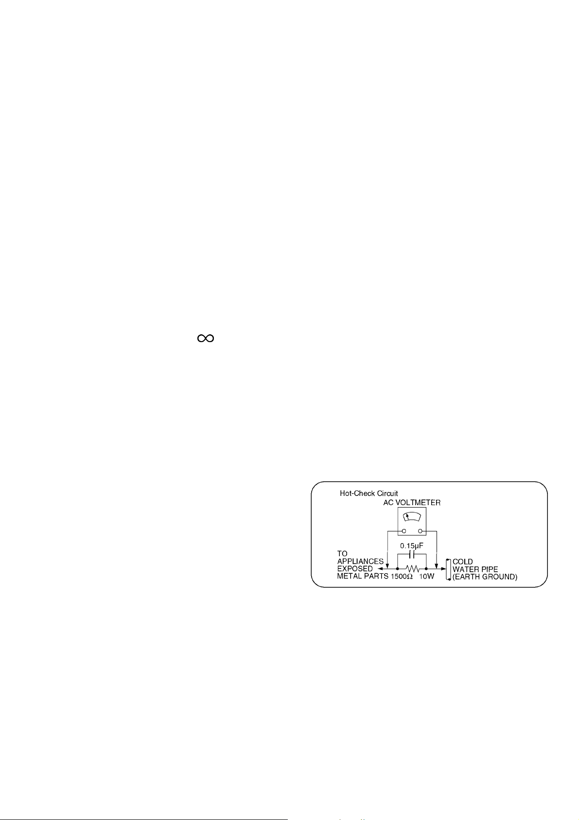
1.1.2. Leakage Current Hot Check (See Figure 1.)
1. Plug the AC cord directly into the AC outlet. Do not use
an isolation transformer for this check.
2. Connect a 1.5kohm, 10 watts resistor, in parallel with a
0.15F capacitors, between each exposed metallic part
on the set and a good earth ground such as a water pipe,
as shown in Figure 1.
3. Use an AC voltmeter, with 1000 ohms/volt or more
sensitivity, to measure the potential across the resistor.
4. Check each exposed metallic part, and measure the
voltage at each point.
5. Reverse the AC plug in the AC outlet and repeat each of
the above measurements.
6. The potential at any point should not exceed 0.75 volts
RMS. A leakage current tester (Simpson Model 229 or
equivalent) may be used to make the hot checks, leakage
current must not exceed 1/2 milliamp. In case a
measurement is outside of the limits specified, there is a
possibility of a shock hazard, and the equipment should
be repaired and rechecked before it is returned to the
customer.
Figure 1
3
Page 4

2Warning
2.1. Prevention of Electrostatic Discharge (ESD) to Electrostatically Sensitive (ES) Devices
Some semiconductor (solid state) devices can be damaged easily by static electricity. Such components commonly are called
Electrostatically Sensitive (ES) Devices. Examples of typical ES devices are integrated circuits and some field-effect transistors and
semiconductor [chip] components. The following techniques should be used to help reduce the incidence of component damage
caused by electrostatic discharge (ESD).
1. Immediately before handling any semiconductor component or semiconductor-equipped assembly, drain off any ESD on your
body by touching a known earth ground. Alternatively, obtain and wear a commercially available discharging ESD wrist strap,
which should be removed for potential shock reasons prior to applying power to the unit under test.
2. After removing an electrical assembly equipped with ES devices, place the assembly on a conductive surface such as
aluminum foil, to prevent electrostatic charge buildup or exposure of the assembly.
3. Use only a grounded-tip soldering iron to solder or unsolder ES devices.
4. Use only an anti-static solder removal device. Some solder removal devices not classified as [anti-static (ESD protected)] can
generate electrical charge sufficient to damage ES devices.
5. Do not use freon-propelled chemicals. These can generate electrical charges sufficient to damage ES devices.
6. Do not remove a replacement ES device from its protective package until immediately before you are ready to install it. (Most
replacement ES devices are packaged with leads electrically shorted together by conductive foam, aluminum foil or
comparable conductive material).
7. Immediately before removing the protective material from the leads of a replacement ES device, touch the protective material
to the chassis or circuit assembly into which the device will be installed.
Caution
Be sure no power is applied to the chassis or circuit, and observe all other safety precautions.
8. Minimize bodily motions when handling unpackaged replacement ES devices. (Otherwise ham less motion such as the
brushing together of your clothes fabric or the lifting of your foot from a carpeted floor can generate static electricity (ESD)
sufficient to damage an ES device).
4
Page 5
2.2. About lead free solder (PbF)
Note: Lead is listed as (Pb) in the periodic table of elements.
In the information below, Pb will refer to Lead solder, and PbF will refer to Lead Free Solder.
The Lead Free Solder used in our manufacturing process and discussed below is (Sn+Ag+Cu).
That is Tin (Sn), Silver (Ag) and Copper (Cu) although other types are available.
This model uses Pb Free solder in it
suggest the use of Pb free solder as well, although Pb solder may be used.
PCBs manufactured using lead free solder will have the PbF within a leaf Symbol PbF stamped on the back of PCB.
Caution
• Pb free solder has a higher melting point than standard solder. Typically the melting point is 50 ~ 70 F (30~40 C) higher. Please
use a high temperature soldering iron and set it to 700 ± 20 F (370 ± 10 C).
• Pb free solder will tend to splash when heated too high (about 1100 F or 600 C).
If you must use Pb solder, please completely remove all of the Pb free solder on the pins or solder area before applying Pb
solder. If this is not practical, be sure to heat the Pb free solder until it melts, before applying Pb solder.
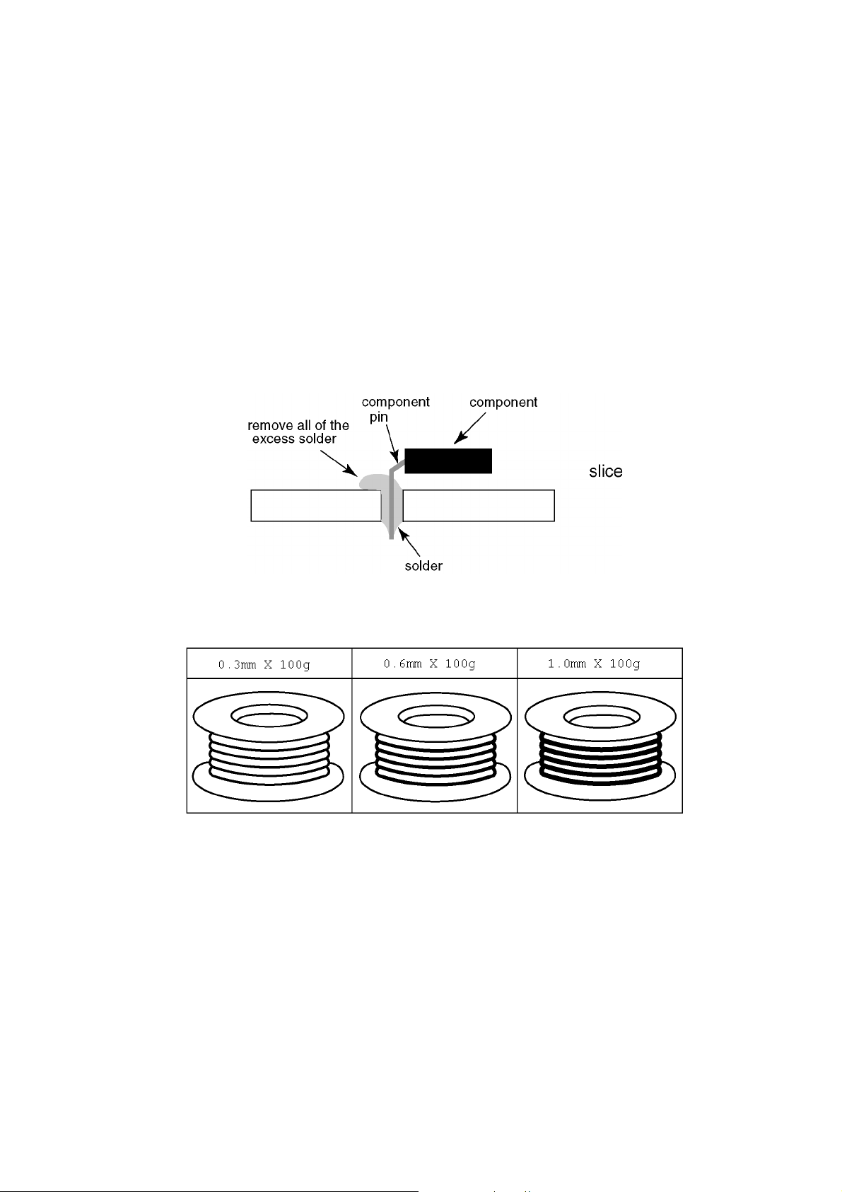
• After applying PbF solder to double layered boards, please check the component side for excess solder which may flow onto the
opposite side. (see figure below)
Suggested Pb free solder
There are several kinds of Pb free solder available for purchase. This product uses Sn+Ag+Cu (tin, silver, copper) solder.
However, Sn+Cu (tin, copper), Sn+Zn+Bi (tin, zinc, bismuth) solder can also be used.
's manufacture due to environmental conservation issues. For service and repair work, we'd
5
Page 6
3 Service Navigation
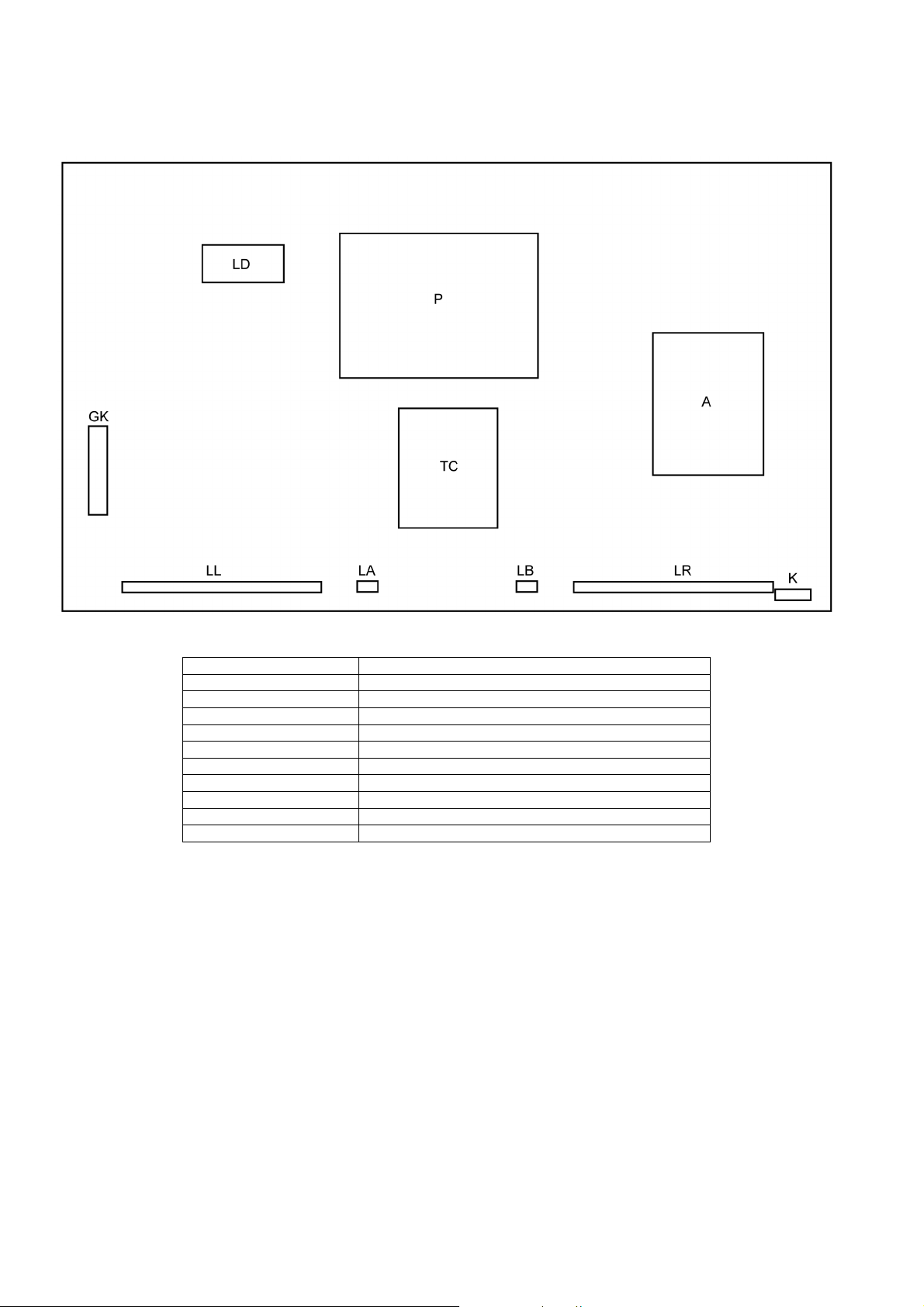
3.1. PCB Layout
Board Name Function
A-Board Main
K-Board IR/LED/AI
P-Board Power
GK-Board SW
LD-Board LED Driver
TC-Board TCON
LL-Board Logo LED
LR-Board Logo LED
LA-Board Logo LED
LB-Board Logo LED
6
Page 7

4 Specifications
Power Source AC 110-127 V, 60 Hz
Power Consumption
Rated Power 190 W
Standby Power 0.2 W
Display Panel
Panel System LCD panel (LED backlight)
Screen size 55 inch class (54.6 inches measured diagonally)
W H Diagonal 47.6 inch 26.7 inch 54.6 inch (1,210 mm 680 mm 1,388 mm)
Number of pixels 1,920 1,080
Speaker Output 18 W [4 W + 4 W + 10 W] ( 10 % THD )
Channel Capability (Digital/Analog) VHF/ UHF: 2 - 69, CATV: 1 - 135
Operating Conditions Temperature: 32 F - 95 F (0 C - 35C)
Humidity: 20 % - 80 % RH (non-condensing)
Connection Terminals
VIDEO IN RCA PIN (VIDEO, AUDIO-L, AUDIO-R)
COMPONENT IN RCA PIN (Y, PB, PR, AUDIO-L, AUDIO-R)
HDMI IN 1/2/3 TYPE A Connector (supports [HDAVI Control 5] function)
USB 1/2 USB 2.0 Type A connector DC 5V, Max. 500mA
DIGITAL AUDIO OUT PCM / Dolby Digital, Fiber Optic
OTHERS SD CARD slot, ETHERNET (10BASE-T/100BASE-TX)
Dimensions (W H D)
Including pedestal 48.3 inch 32.1 inch 14.1 inch (1,227 mm 814 mm 358 mm)
TV Set only 48.3 inch 28.2 inch 1.3 inch (1,227 mm 717 mm 32 mm)
Mass
Including pedestal 44.1 lb. (20.0 kg) NET
TV Set only 35.3 lb. (16.0 kg) NET
■ Built-in Camera
Lens F2.0 Lens; FOV (D) 50.9° (in HD mode)
Focus Fixed focus
Resolution 1280 x 720
■ Wireless LAN
Standard Compliance and
Frequency Range*
Security WPA2-PSK (TKIP/AES)
1
The frequency and channel differ depending on the country.
*
2
802.11b/g/n CH1 ~ CH11 only use for United States and Canada.
*
1,*2
IEEE 802.11a/n:
5.15 GHz - 5.35 GHz, 5.47 GHz - 5.85 GHz
IEEE 802.11b/g/n:
2.400 GHz - 2.4835 GHz
WAP-PSK (TKIP/AES)
WEP (64bit/128bit)
■ Bluetooth
Standard Compliance Bluetooth 3.0
Frequency Range 2.402GHz - 2.480 GHz
Note
Design and Specifications are subject to change without notice. Mass and Dimensions shown are approximate.
Use Panasonic 3D Eyewear supporting passive 3D system technology.
VIERA Touch Pad Controller uses Bluetooth wireless technology.
7
Page 8

5 Technical Descriptions
5.1. Specification of KEY for DTCP-IP, WMDRM and Widevine
5.1.1. General information:
1. NAND Flash (IC8900) for spare parts has the seed of KEY for each DTCP-IP for DLNA, WMDRM for Netflix and Widevine for
CinemaNow.
2. The final KEY data will be generated by Main IC (IC8000) when SELF CHECK was done and are stored in both Main IC
(IC8000) and NAND Flash (IC8900).
5.1.2. Replacement of ICs:
When Main IC is replaced, NAND Flash should be also replaced with new one the same time.
When NAND Flash is replaced, Main IC is not necessary to be replaced the same time.
After the replacement of IC, SELF CHECK should be done to generate the final KEY data.
How to SELF CHECK: While pressing [VOLUME ( - )] button on the main unit, press [MENU] button on the remote control for
more than 3 seconds.
TV will be forced to the factory shipment setting after this SELF CHECK.
8
Page 9
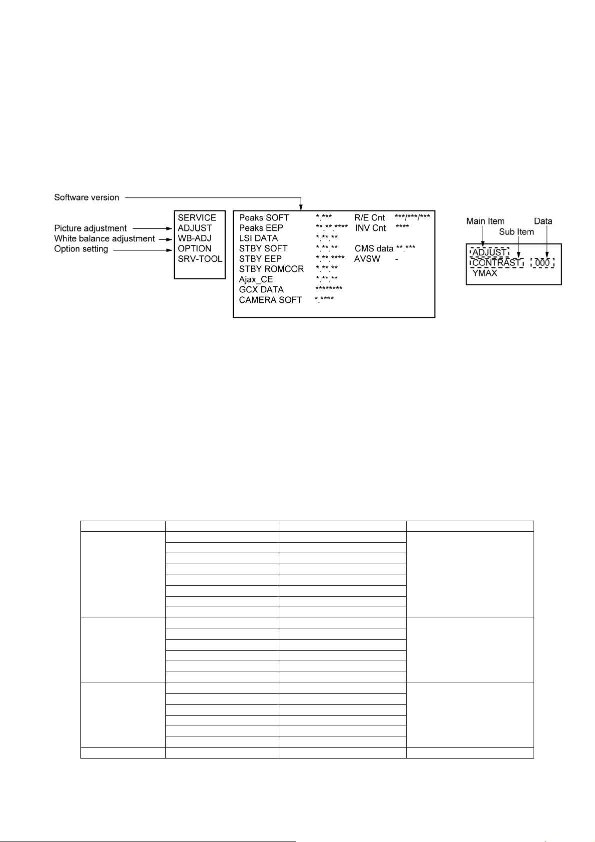
6 Service Mode
6.1. How to enter into Service Mode
6.1.1. Purpose/
After exchange parts, check and adjust the contents of adjustment mode.
While pressing [VOLUME ( - )] button of the main unit, press [INFO] button of the remote control three times within 2 seconds.
Note:
Service Mode can not be entered when 3D signal input.
Input 2D signal to enter Service Mode.
6.1.2. Key command
[1] button...Main items Selection in forward direction
[2] button...Main items Selection in reverse direction
[3] button...Sub items Selection in forward direction
[4] button...Sub items Selection in reverse direction
[VOL] button...Value of sub items change in forward direction ( + ), in reverse direction ( - )
6.1.3. How to exit
Switch off the power with the [POWER] button on the main unit or the [POWER] button on the remote control.
6.1.4. Contents of adjustment mode
• Value is shown as a hexadecimal number.
• Preset value differs depending on models.
• After entering the adjustment mode, take note of the value in each item before starting adjustment.
Main item Sub item Sample Data Remark
ADJUST CONTRAST 000
COLOR 3A
TINT 00
SUB-BRT 800
BACKLGT FFF
B-Y-G 40
R-Y-A 00
V COM 000
WB-ADJ R-GAIN 80
G-GAIN 76
B-GAIN 59
R-CENT 82
G-CENT 80
B-CENT 6D
OPTION Boot ROM Factory Preset.
STBY-SET 00
EMERGENCY ON
CLK MODE 01
CLOCK FFF
EDID-CLK HIGH
SRV-TOOL 00 See next.
9
Page 10
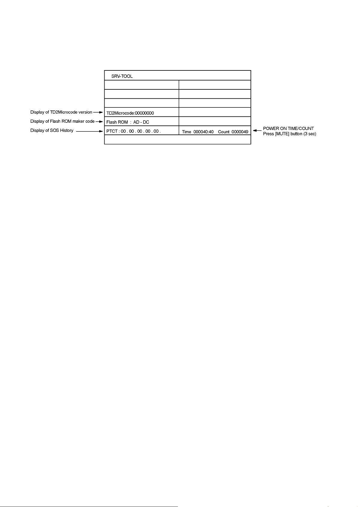
6.2. SRV-TOOL
6.2.1. How to access
1. Select [SRV-TOOL] in Service Mode.
2. Press [OK] button on the remote control.
6.2.2. Display of SOS History
SOS History (Number of LED blinking) indication.
From left side; Last SOS, before Last, three occurrence before, 2nd occurrence after shipment, 1st occurrence after shipment.
This indication except 2nd and 1st occurrence after shipment will be cleared by [Self-check indication and forced to factory
shipment setting].
6.2.3. POWER ON TIME/COUNT
Note : To display TIME/COUNT menu, highlight position, then press MUTE for 3 sec.
Time : Cumulative power on time, indicated hour : minute by decimal
Count : Number of ON times by decimal
Note : This indication will not be cleared by either of the self-checks or any other command.
6.2.4. Exit
Disconnect the AC cord from wall outlet or press the [POWER] button on the main unit for 3 seconds to turn off and then turn on
automatically.
10
Page 11
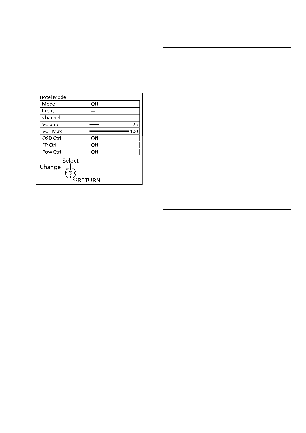
6.3. Hotel mode
1. Purpose
Restrict a function for hotels.
2. Access command to the Hotel mode setup menu
In order to display the Hotel mode setup menu:
While pressing [VOLUME (-)] button of the main unit,
press [INPUT] button of the remote control three times
within 2 seconds.
Then, the Hotel mode setup menu is displayed.
3. To exit the Hotel mode setup menu
Switch off the power with the [POWER] button on the
main unit or the [POWER] button on the remote control.
4. Explain the Hotel mode setup menu
Item Function
Mode Select hotel mode On/Off
Input Select input signal modes.
Set the input, when each time power is
switched on.
Selection:
-,RF,HDMI1,HDMI2,HDMI3,AV
• Off: give priority to a last memory.
Channel Select channel when input signal is RF.
Set the channel, each time power is switched
on.
Selection:
Any channel number or [-].
[-] means the channel when turns off.
Volume Adjust the volume when each time power is
switched on.
Range:
0 to 100
Vol. Max Adjust maximum volume.
Range:
0 to 100
OSD Ctrl Restrict the OSD.
Selection:
Off/Pattern1
• Off: No restriction
• Pattern1: restriction
FP Ctrl Select front key conditions.
Selection:
Off/Pattern1/All
• Off: altogether valid.
• Pattern1: only input key is valid.
• All: altogether invalid.
Pow Ctrl Select POWER-On/Off condition when AC
power cord is disconnected and then
connected.
Off: The same condition when AC power
cord is disconnected.
On: Forced power ON condition.
11
Page 12
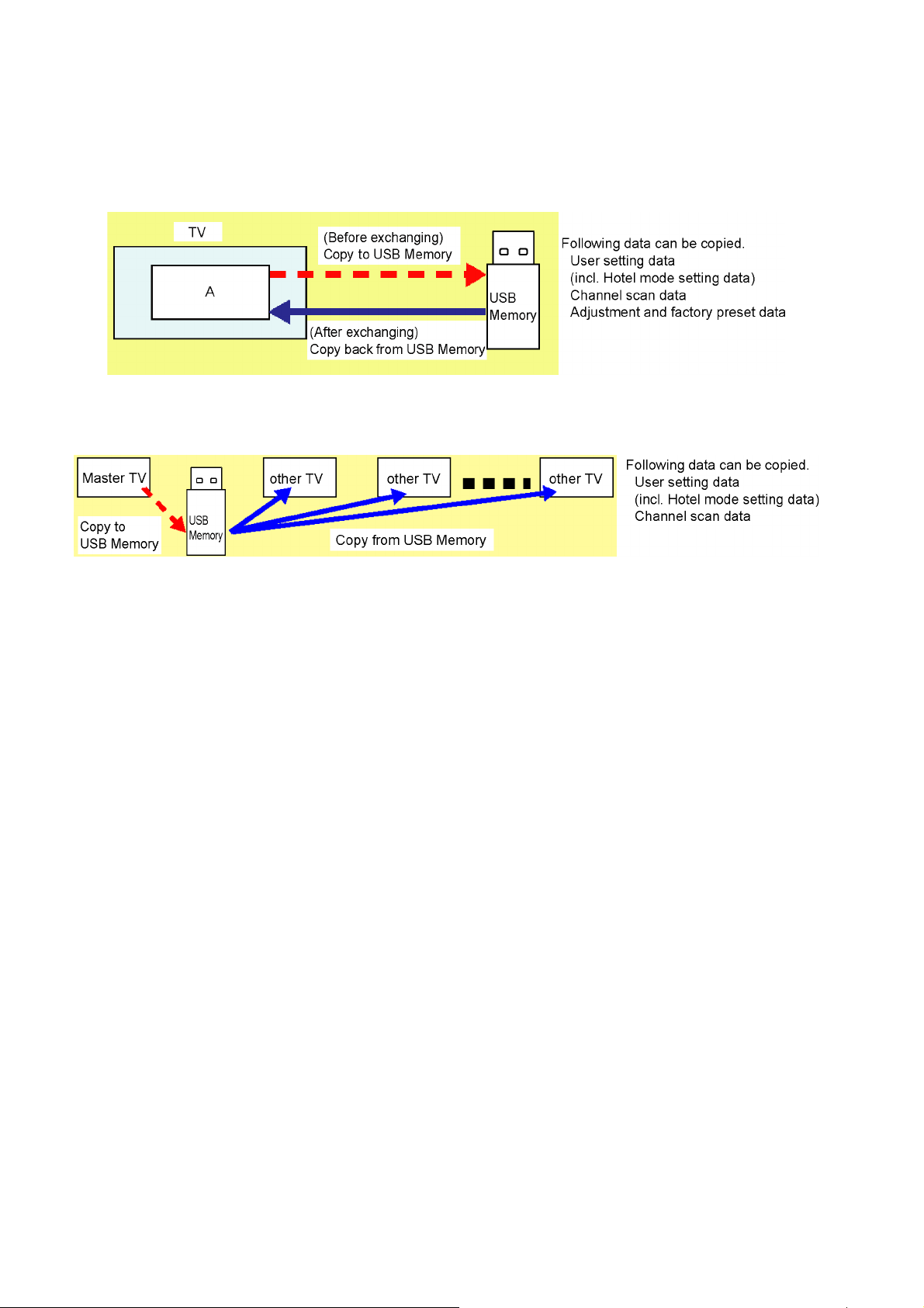
6.4. Data Copy by USB Memory
Note:
SD card can not be used for Data Copy.
6.4.1. Purpose
(a) Board replacement (Copy the data when exchanging A-board):
When exchanging A-board, the data in original A-board can be copied to USB Memory and then copy to new A-board.
(b) Hotel (Copy the data when installing a number of units in hotel or any facility):
When installing a number of units in hotel or any facility, the data in master TV can be copied to USB Memory and then copy to
other TVs.
6.4.2. Preparation
Make pwd file as startup file for (a) or (b) in a empty USB Memory.
1. Insert a empty USB Memory to your PC.
2. Right-click a blank area in a USB Memory window, point to New, and then click text document. A new file is created by default
(New Text Document.txt).
3. Right-click the new text document that you just created and select rename, and then change the name and extension of the
file to the following file name for (a) or (b) and press ENTER.
File name:
(a) For Board replacement : boardreplace.pwd
(b) For Hotel : hotel.pwd
Note:
Please make only one file to prevent the operation error.
No any other file should not be in USB Memory.
12
Page 13
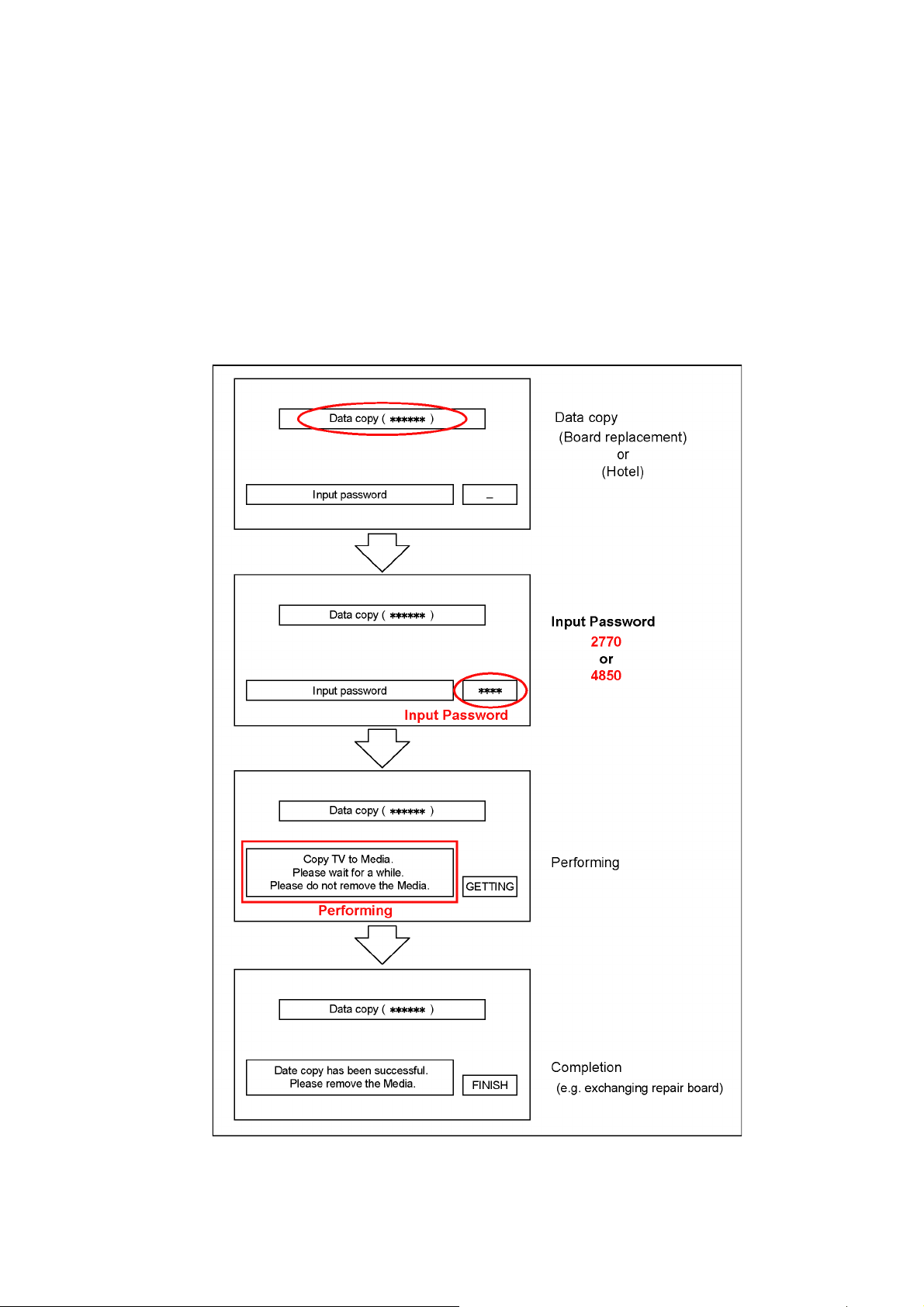
6.4.3. Data copy from TV set to USB Memory
1. Turn on the TV set.
2. Insert USB Memory with a startup file (pwd file) to USB terminal.
On-screen Display will be appeared according to the startup file automatically.
3. Input a following password for (a) or (b) by using remote control.
(a) For Board replacement : 2770
(b) For Hotel : 4850
Data will be copied from TV set to USB Memory.
It takes around 2 to 6 minutes maximum for copying.
4. After the completion of copying to USB Memory, remove USB Memory from TV set.
5. Turn off the TV set.
Note:
Following new folder will be created in USB Memory for data from TV set.
(a) For Board replacement : user_setup
(b) For Hotel : hotel
13
Page 14
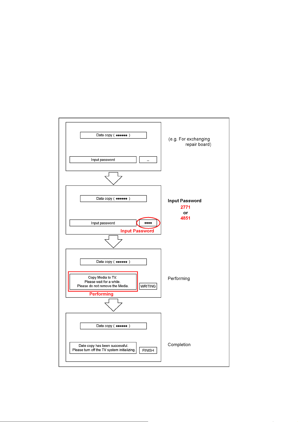
6.4.4. Data copy from USB Memory to TV set
1. Turn on the TV set.
2. Insert USB Memory with Data to USB terminal.
On-screen Display will be appeared according to the Data folder automatically.
3. Input a following password for (a) or (b) by using remote control.
(a) For Board replacement : 2771
(b) For Hotel : 4851
Data will be copied from USB Memory to TV set.
4. After the completion of copying to USB Memory, remove USB Memory from TV set.
(a) For Board replacement : Data will be deleted after copying (Limited one copy).
(b) For Hotel : Data will not be deleted and can be used for other TVs.
5. Turn off the TV set.
Note:
1. Depending on the failure of boards, function of Data copy for board replacement does not work.
2. This function can be effective among the same model numbers.
14
Page 15
7 Troubleshooting Guide
Use the self-check function to test the unit.
1. Checking the IIC bus lines
2. Power LED Blinking timing
7.1. Check of the IIC bus lines
7.1.1. How to access
7.1.1.1. Self-check indication only:
Produce TV reception screen, and while pressing [VOLUME ( - )] button on the main unit, press [OK] button on the remote control
for more than 3 seconds.
7.1.1.2. Self-check indication and forced to factory shipment setting:
Produce TV reception screen, and while pressing [VOLUME ( - )] button on the main unit, press [MENU] button on the remote
control for more than 3 seconds.
7.1.2. Exit
Disconnect the AC cord from wall outlet or press the [POWER] button on the main unit for 3 seconds to turn off and then turn on
automatically.
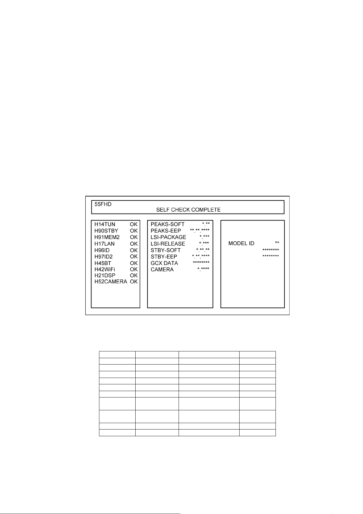
7.1.3. Screen display
7.1.4. Check Point
Confirm the following parts if NG was displayed.
DISPLAY Check Ref. No. Description Check Point
H14TUN TU6706 TUNER A-Board
H90STBY IC8000 STM A-Board
H91MEM2 IC8900 NAND FLASH A-Board
H17LAN IC8600, JK8650A LAN A-Board
H96ID ID
H97ID2 ID2
H45BT IC8458 Bluetooth A-Board
H42WiFi IC8458 WiFi A-Board
H21DSP IC4900 DIGITAL SOUND PRO A-Board
H52CAMERA CAMERA Camera
BT Dongle
WiFi Dongle
15
Page 16

7.2. Power LED Blinking timing chart
1. Subject
Information of LED Flashing timing chart.
2. Contents
When an abnormality has occurred the unit, the protection circuit operates and reset to the stand by mode. At this time, the
defective block can be identified by the number of blinks of the Power LED on the front panel of the unit.
Blinking Times Contents Check point
1 BACK LIGHT SOS LCD PANEL
P-Board
7 SUB 3.3V SENSE SOS A-Board
9 SOUND SOS A-Board
13 EMERGENCY SOS A-Board
Speaker
7.3. LCD Panel test mode
Purpose:
To find the possible failure point where in LCD Panel or Printed Circuit Board when the abnormal picture is displayed.
How to Enter:
While pressing [VOLUME ( - )] button of the main unit, press [OPTION] button of the remote control three times within 2
seconds.
How to Exit:
Switch off the power with the [POWER] button on the main unit or the [POWER] button on the remote control.
How to confirm:
If the abnormal picture is displayed, go into LCD Panel test mode to display the several test patterns.
And then, judge by the following method.
Still abnormal picture is displayed: The cause must be in LCD Panel.
Normal picture is displayed: The cause must be in A board.
Remarks:
The test pattern is created by the circuit in LCD Panel.
In LCD Panel test mode, this test pattern is displayed unaffected by signal processing for RF or input signal.
If the normal picture is displayed, LCD Panel must be okay and the cause of failure must be in A board.
16
Page 17
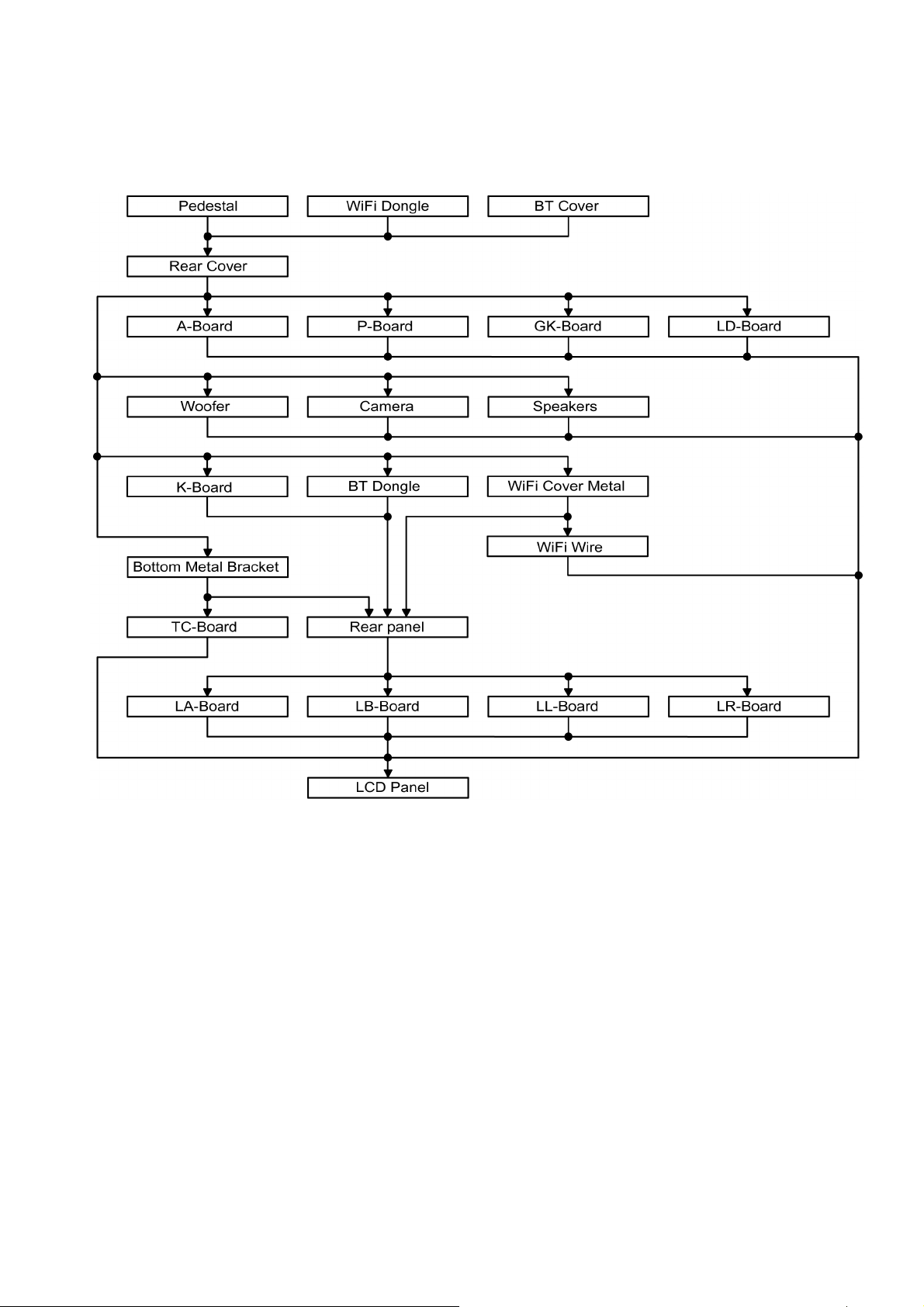
8 Disassembly and Assembly Instructions
8.1. Disassembly Flow Chart for the Unit
This is a disassembly chart.
When assembling, perform this chart conversely.
17
Page 18
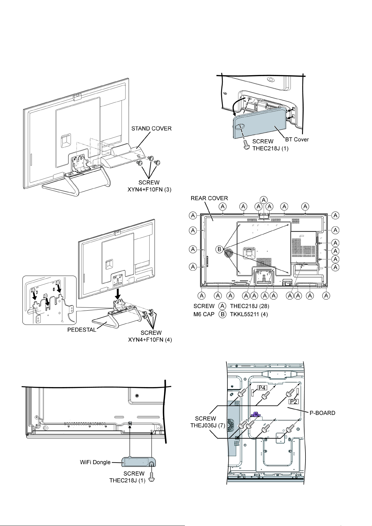
8.2. Disassembly Procedure for the Unit
8.2.1. Pedestal
1. Lay down the unit so that the rear cover faces upward.
2. Remove the 3 screws.
3. Remove the pedestal cover.
4. Remove the 4 screws.
5. Remove the pedestal.
8.2.3. Bluetooth Cover
1. Remove the 1 screw.
2. Remove the Bluetooth Cover.
8.2.4. Back Cover
1. Remove the 28 screws.
2. Remove the 4 M6 CAPs.
3. Remove the Back Cover.
8.2.2. WiFi Dongle
1. Remove the 1 screw.
2. Remove the WiFi Dongle.
8.2.5. P-Board
1. Remove the 7 screws.
2. Disconnect the connectors (P2 and P4).
3. Remove the P-Board.
18
Page 19
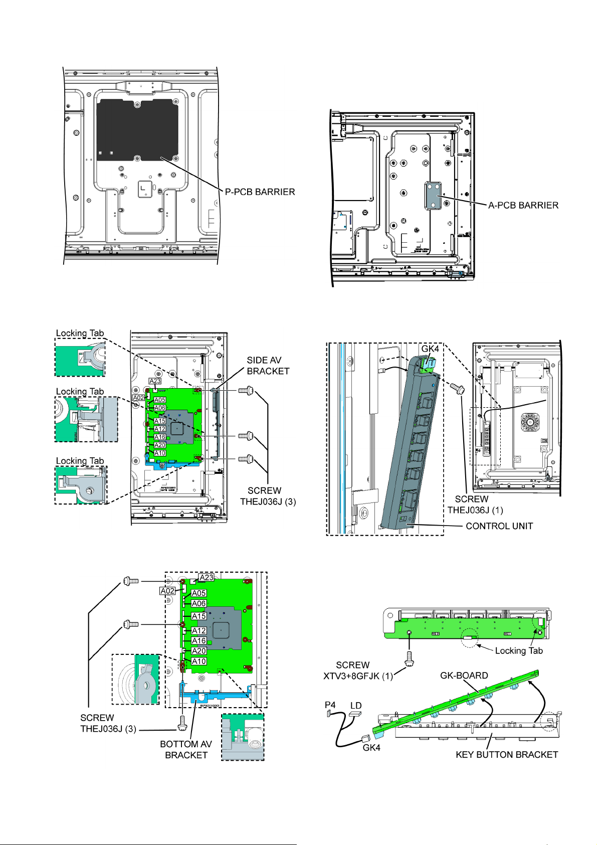
4. Remove the P-PCB Barrier.
8.2.6. A-Board
1. Remove the 3 screws.
2. Remove the Side AV Bracket.
5. Disconnect the connectors (A02, A05, A06, A10, A12,
A15, A16, A20 and A23).
6. Remove the A-Board.
7. Remove the A-PCB Barrier.
8.2.7. GK-Board
1. Remove the 1 screw.
3. Remove the 3 screws.
4. Remove the Bottom AV Bracket.
2. Remove the 1 screw.
3. Remove the 2 locking tabs.
4. Disconnect the connector (GK4).
5. Remove the GK-Board and the Key Button Bracket.
19
Page 20
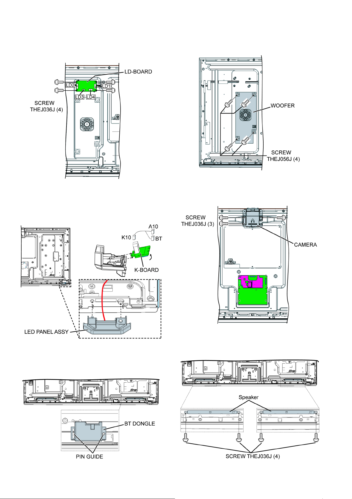
8.2.8. LD-Board
1. Remove the 4 screws.
2. Disconnect the connector (LD1, LD2, LD3 and LD4).
3. Remove the LD-Board.
8.2.9. K-Board
1. Remove the LED panel assy.
2. Disconnect the connector (K10).
3. Remove the K-Board.
8.2.11. Woofer
1. Remove the 4 screws.
2. Remove the Woofer.
8.2.12. Camera
1. Remove the 3 screws.
2. Remove the Camera.
8.2.10. Bluetooth Dongle
1. Disconnect the connector .
2. Remove the BT-Dongle.
8.2.13. Speakers
1. Remove the 4 screws.
2. Remove the 2 Speakers.
20
Page 21
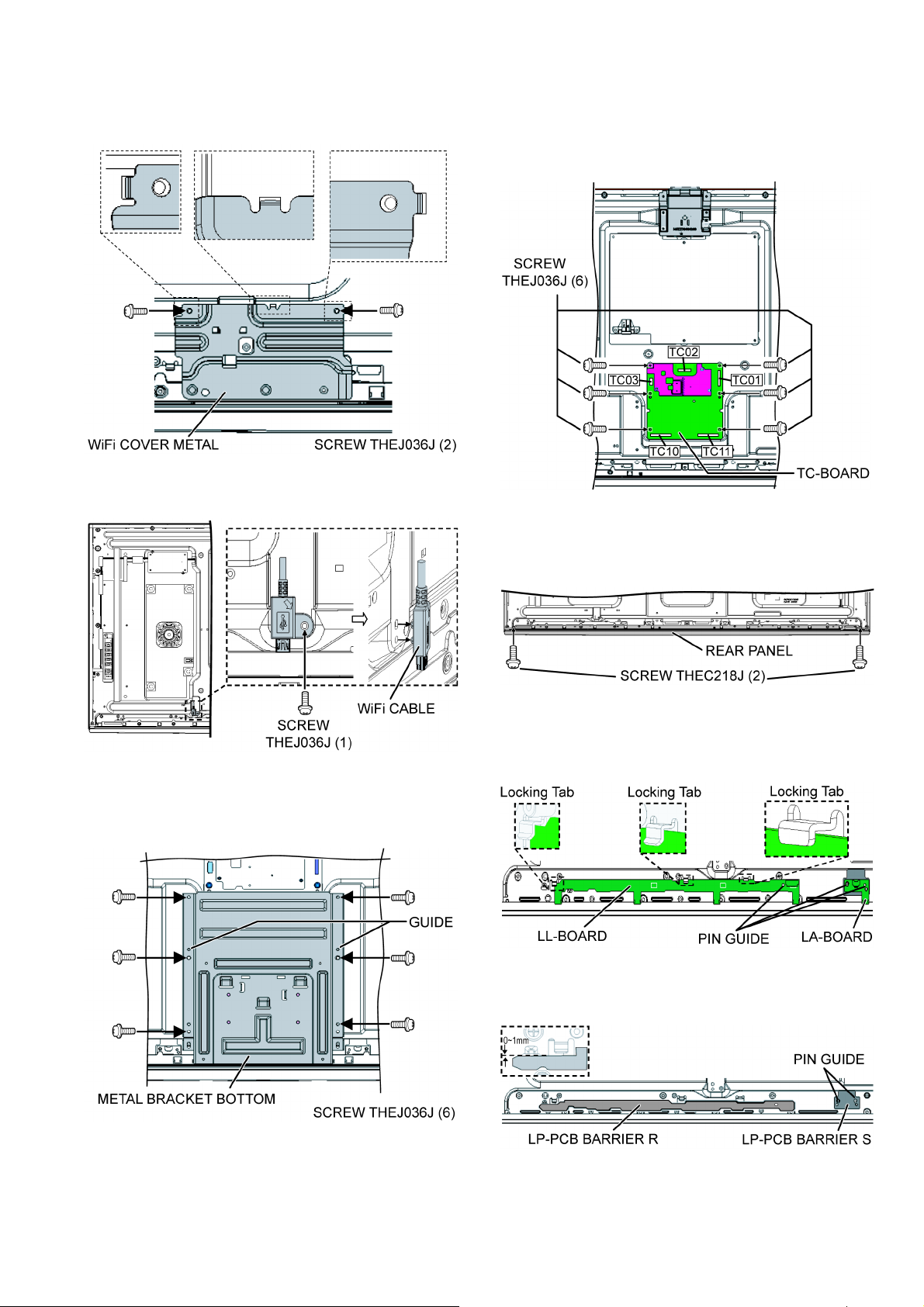
8.2.14. WiFi Cover Metal
1. Remove the 2 screw.
2. Remove the WiFi cover metal.
3. Remove the 1 screw.
4. Remove the WiFi cable.
8.2.16. TC-Board
1. Remove the 6 screws.
2. Disconnect the connectors (TC01, TC02, TC03, TC10
and TC11).
3. Remove the TC-Board.
8.2.17. Rear Panel
1. Remove the 2 screws.
2. Remove the Rear Panel.
8.2.15. Metal Bracket Bottom
1. Remove the 6 screws.
2. Remove the Metal Bracket Bottom.
8.2.18. LL-Board and LA-Board
1. Remove the 3 Locking Tabs.
2. Remove the LL-Board and LA-Board.
8.2.19. LP-PCB Barrier R and S
1. Remove the LP-PCB Barrier L and .
21
Page 22
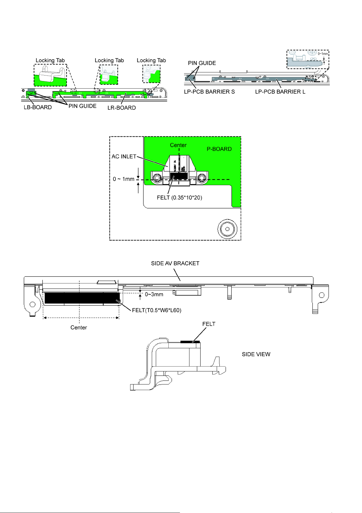
8.2.20. LR-Board and LB-Board
1. Remove the 3 Locking Tabs.
2. Remove the LR-Board and LB-Board.
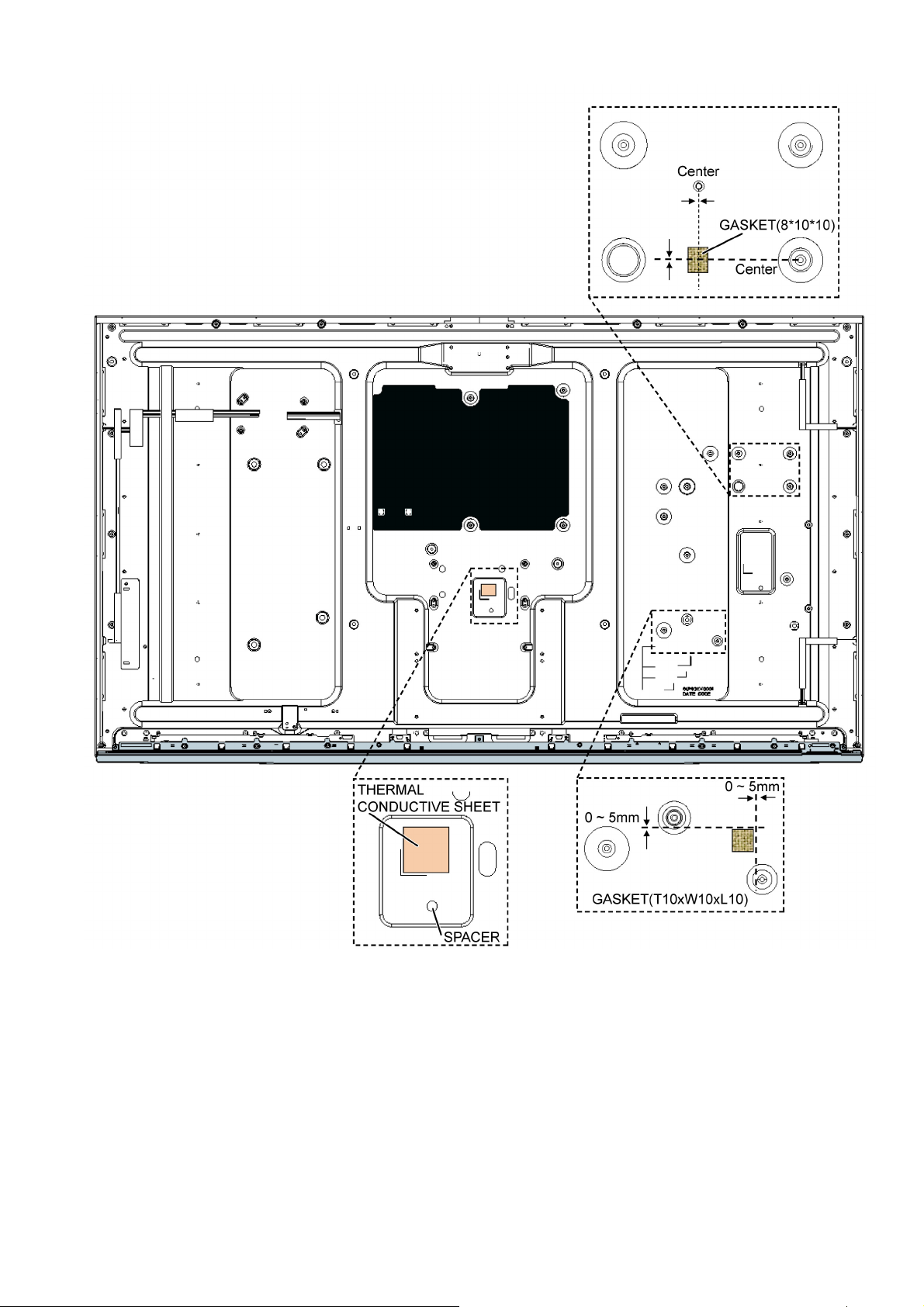
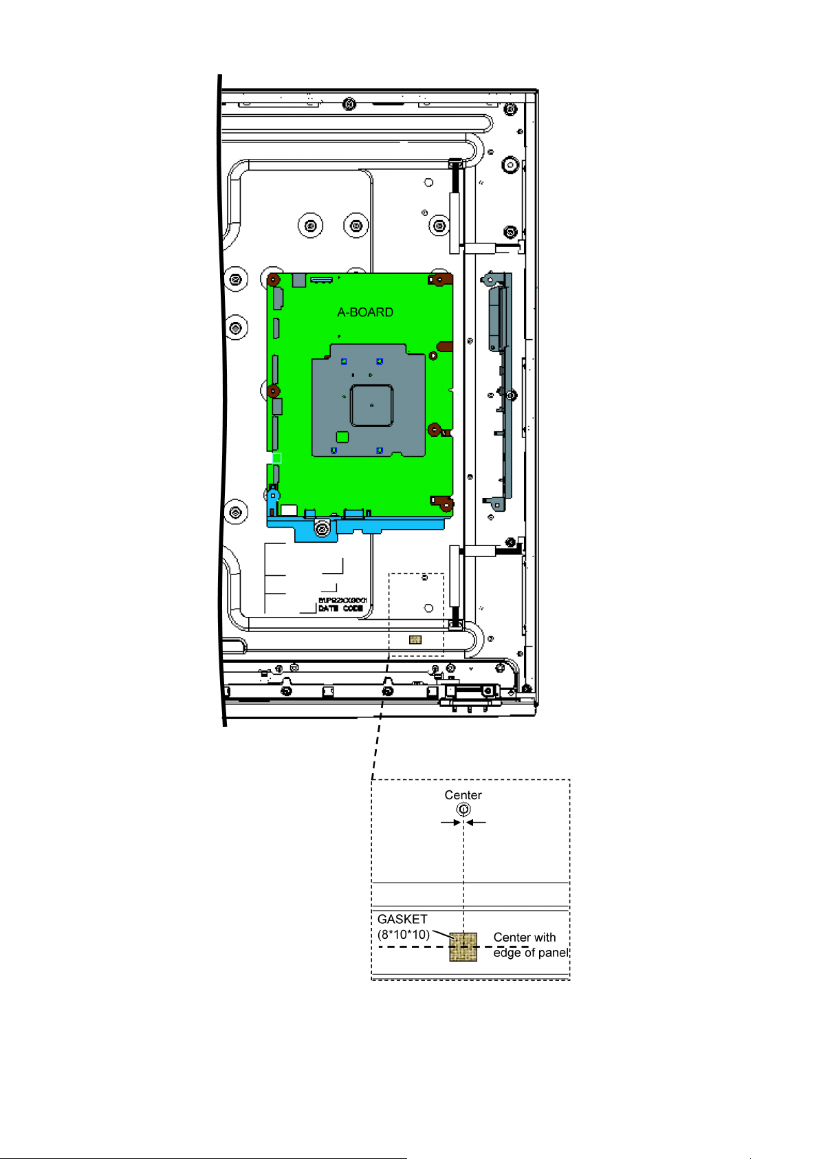
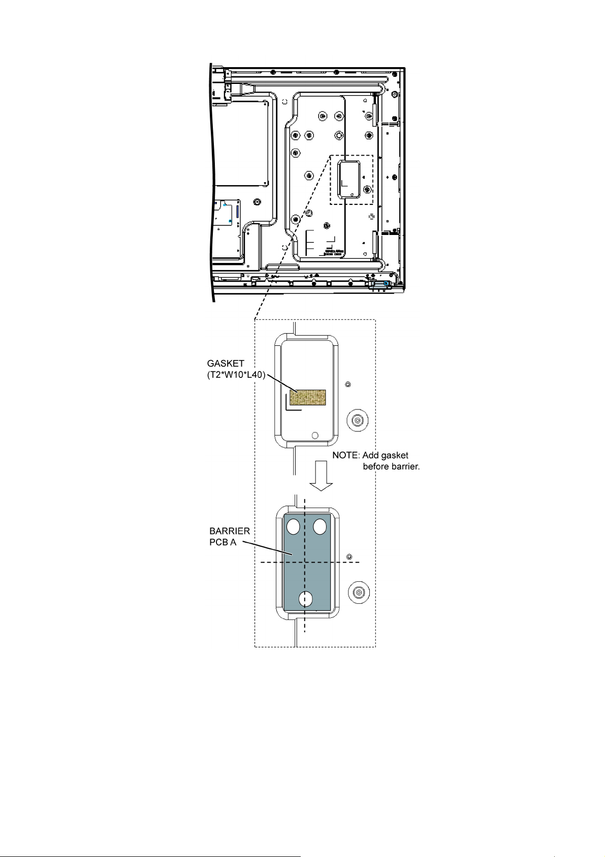
8.2.22. Felt, Sponge, and so on.
8.2.21. LP-PCB Barrier L and S
1. Remove the LP-PCB Barrier L and S.
22
Page 23
2324252627
Page 24
Page 25
Page 26
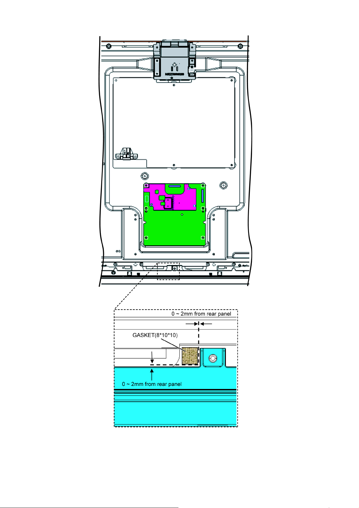
Page 27
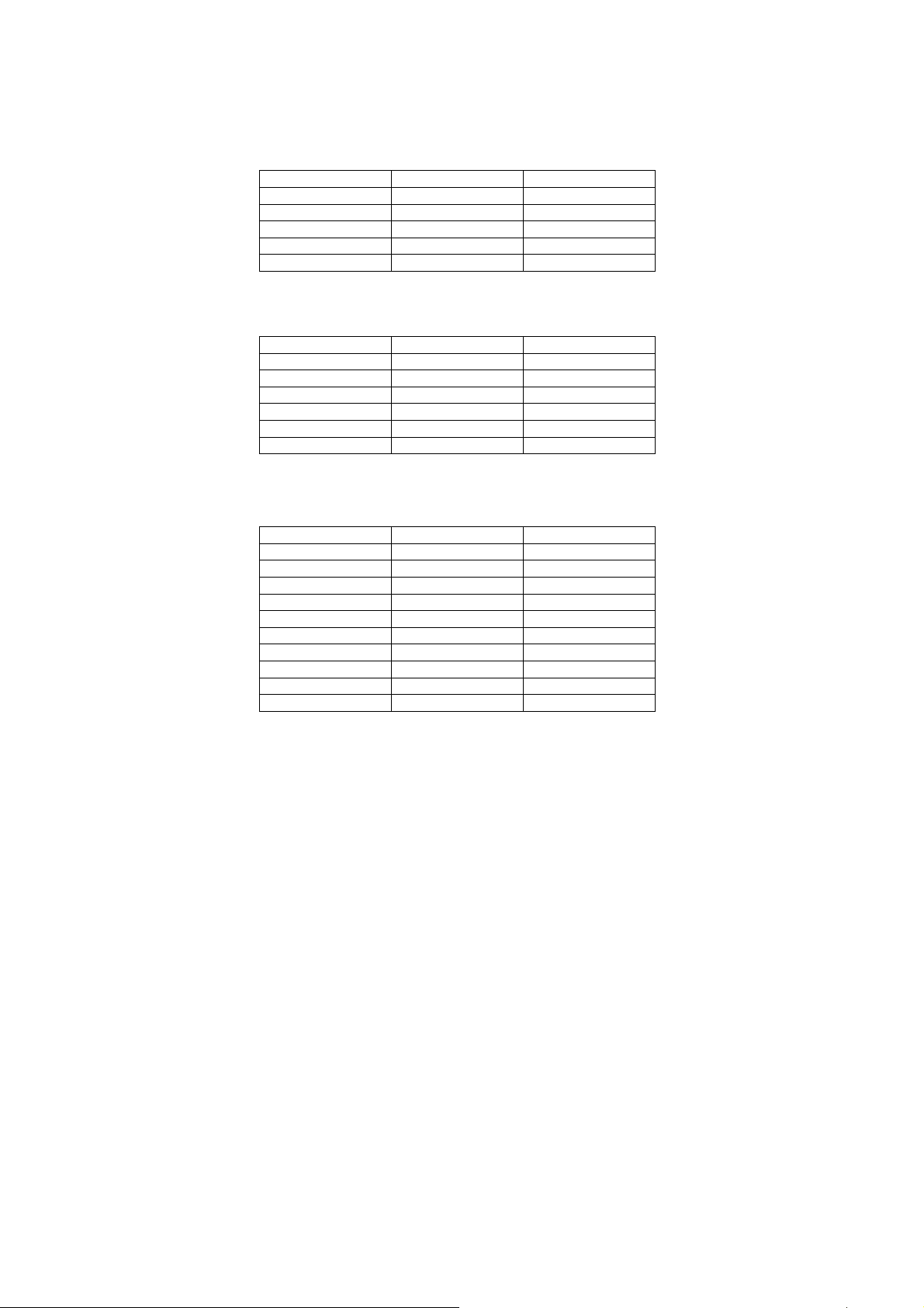
9 Measurements and Adjustments
9.1. Voltage chart of P-board
Power Supply Name Test point Spec
40V TP7401 40±3V
16V TP7410 15.7±0.6V
5VS TP7501 5.3±0.2V
VLED TP7409 84V±5V
PFC TP7201 or TP7202 390V ±15V *HOT
9.2. Voltage chart of A-board
Power Supply Name Test point Spec
USB5V TP5440 5.00V - 5.40V
SUB5V TP5420 4.92V - 5.25V
SUB3.3V TP5400 3.17V - 3.45V
SUB1.8V TP8714 1.70V - 1.90V
SUB1.5V TP8101 1.38V - 1.54V
SUB1.1V TP8100 1.00V - 1.24V
9.3. Voltage chart of TC-board
Power Supply Name Test point Spec
GCX3.3V TP9151 3.17V - 3.43V
GCX1.5V TP9501 1.38V - 1.54V
GCX1.1V TP9500 1.10V - 1.24V
PNL12V TP4314 11.50V - 12.50V
VCC3.3V TP4185 3.1V - 3.5V
VCORE1.2V TP4184 1.1V - 1.3V
VDD16.5V TP4181 16.30V - 16.70V
HVDD8V TP4186 7.65V - 7.85V
VGH26V TP4182 26.7 - 27.32
VGL-5V TP4183 -5.6V - -5.2V
Page 28
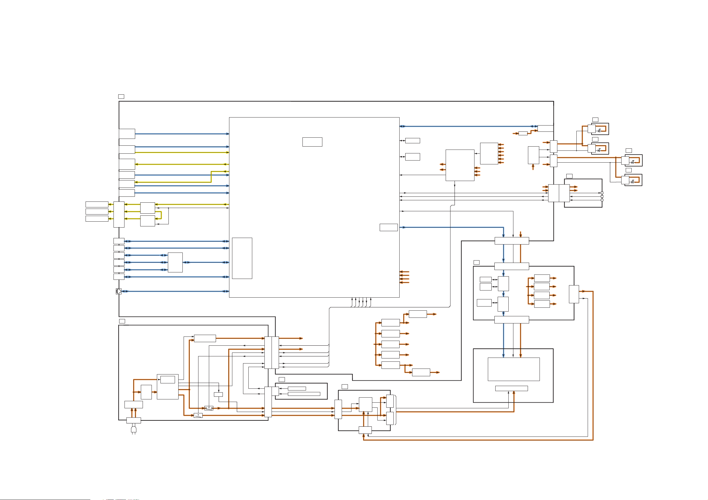
10 Block Diagram
10.1. Main Block Diagram
A
MAIN
IF
TUNER
Y/PB/PR
AV
L/R
DIGITAL
AUDIO
OUT
TMDS DATA
HDMI1
ARC
TMDS DATA
HDMI2
TMDS DATA
HDMI3
A12
USB1
USB3
USB2
A20
A10
A23
P
AC CORD
POWER
INPUT
FILTER
LIVE
JK7101
L
AUDIO
R
AMP
W
AUDIO
AMP
PFC
NEUTRAL
SPEAKER(L)
SPEAKER(R)
WOOFER
WiFi
BT
CAMERA
ETHERNET
AC
DETECT
LLC
CONVERTER
USB
HUB
REG
IF
COMPONENT IN
CVBS IN
L/R IN
SPDIF_OUT
ARC_OUT
HDMI
I/F
AUDIO_OUT
SOUND_SOS
USB I/F
ETHER I/F
5VS
SUB_ON
16V
BL_SOS
ECO_ON
KEY
POWER_ON
16V
FB
VLED
LL
LL5
LA5
LA
LOGO_LED
LOGO_LED
LED_R
REMOTE RECEIVER
C.A.T.S. SENSOR
LR6
LB6
LR
LB
LOGO_LED
LOGO_LED
Paragon
NAND_I/F
REMOTE IN
C.A.T.S. SENSOR
PANEL_VCC_ON
LVDS Tx
SD IF
DDR_I/F
TV_SOS
LED_R
DDR3
NAND
FLASH
STB3.3V
SUB_AI_3.3V
ANALOG-ASIC
SUB_ON
OVP DET
P15V
SUB5V
STB5V
SD CARD DATA
SUB5V
USB5V
SUB3.3V
SUB1.1V
SUB1.5
SUB5V
P15V
REG
SUB_AI_3.3V
P15V
PANEL_VCC_ON
LOGO
LED
SUB3.3V
STB3.3V
SD CARD
SLOT
P15V
P15V
A05
A06
LED/RM/CATS
K
SUB3.3V
STB3.3V
K10
A10
A15,A16
TC
TCON
STB3.3V
SUB3.3V
KEY
POWER_ON
BL_PWM
SUB_ON
BL_ON
BL_SOS
SUB1.5V
SUB1.2V
DDR3
SPI
8M
EEPROM
DCDC
DCDC
SUB3.3V
DCDC
STB5V
SUB_ON
P15V
BL_SOS
A02
P2
GK4
GK
ECO_ON
KEY
POWER ON
SWITCH
POWER SW
CONTROL PANEL KEY
LD
LED DRIVER
P4
LD4
LED
DRIVER
P15V
USB5V
DCDC
SUB1.5V
DCDC
SUB1.1V
DCDC
SUB5V
LD1
TU_1.8V
SUB3.3V
USB5V
SUB1.5V
SUB1.1V
SUB5V
AVDDH3.3V
DCDC
TU_1.8V
HDMI3.3V
LCD PANEL
TC01,TC02
GCX
TCON
TC10,TC11
PANEL
LED BACK LIGHT
P15V
DCDC
PNL12V
DCDC
GCX3.3V
DCDC
GCX1.5V
DCDC
GCX1.1V
PNL12V
GCX3.3V
GCX1.5V
GCX1.1V
TC03
LD2
LD3
2
Page 29
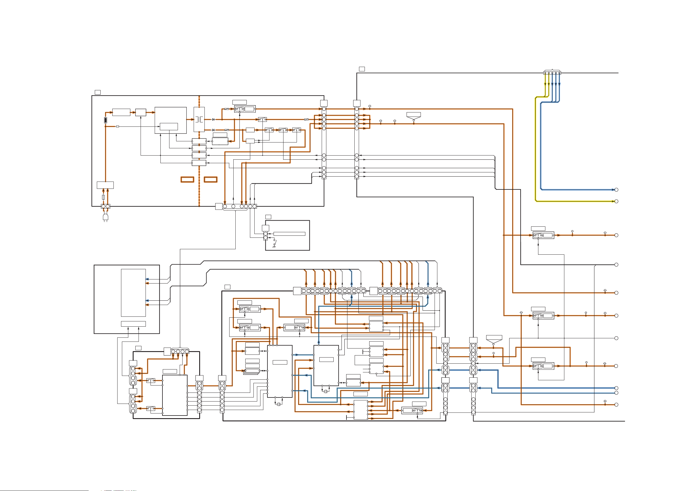
10.2. Block (1/2) Diagram
P
POWER
D7102
RECTIFIER
CF7103
LF7103
LF7104
LF7105
LINE
FILTER
NO
HOLDER
F7101
231
JK7101
AC CORD
IC7201,
T7201,
Q7201
PFC
IC7301,
Q7301,
Q7302
LLC
CONVERTER
AC
DETECT
PC7301
PC7303
PC7302
PC7304
JK3101A
A
MAIN
STB5V
T7302
D748,9
D7401,2
IC7401
PHOTO
COUPLER
PHOTO
COUPLER
PHOTO
COUPLER
PHOTO
COUPLER
HOT
COLD
ERROR
DETECT
P4
PA7406
PA7407
+16V
4
IC7503
FB
6
VLED
2
T7800
IC7800
VLED
1
+5V
12
Q7403,08
KEY
POWER_ON
11
Q7801
GK
Q7804,5
KEY,Power SW
PA7402
Q7422,23
P2
5VS
6
+16V
4
+16V
3
+16V
2
+16V
1
SUB_ON
8
ECO_ON
13
BL_SOS
11
KEY
10
POWER_ON
9
5.8VS
A02
11
7
5
3
1
2
12
8
6
4
P15V
DCDCIN
TP2028
SRV_15V
SUB_ON
ECO_ON
BL_SOS
POWER_ON
KEY
AV
Y
L
R
PB
PR
1
2
LCD PANEL
PANEL
BACK LIGHT
LD1
1
12
3
10
LD2
1
12
3
10
LD
LED DRIVER
Q9801-08
Q9809-16
LD4
IC9800
LED
(K1-K8)
LED
(K9-K16)
VLED
8
9
DVDD
HSYNC
VSYNC
BL_SOS
BL_ON
GK4
SW2851-2855
2
CONTROL PANEL KEY
SW2857
POWER SW
VGH_M30V
HVDD8V
VGL-5V
GMA
VDD16.5V
TC
TCON
IC9503
IC9504
GCX1.1V
+1.1V
GCX1.5V
+1.5V
GCX3.3V
TC11
IC9151
+3.3V
IC9100
4
6
FB
+16V
SPI
8M
IC9501
IC9502
DDR3
LD3
FB
+16V
18
19
14
12
16
CLK
4
8
DVDD3.3
HSYNC
VSYNC
BL_SOS
BL_ON
CLK
TC03
2
3
7
9
5
17
13
SPI
HSYNC
VSYNC
BL_SOS
BL_ON
CLK
IC9500
GCX
X9500
LVDS_RX
SYSTEM
BUS
1
1V2_TCON_M
VCC3.3V_T
2
VCC3.3V
4
5
miniLVDS_TX
LVDS_RXLVDS_TX
7
IC4100
TCON
X4100
11
8
DPM
GSC
16
38
23
VCC3.3V
VCORE1.2V
LLRV/LLV
47
IC4400
EEPROM
IIC
79
VGH_M30V
VCC3.3V
GMA(1-18)
VCOM_PG
VCOM_PG
VCOM_LFB
VCOM_RFB
IC4250
DCDC
IIC
TC10
IC4350
IC4300
IC4301
VCC3.3V
HVDD8V
80
VCOM_OUT
VGL-5V
PNL12V
VGH26V
VDD16.5V
VDD16.5V
79
VGH26V
GSC
DPM
VCC3.3V
VDD16.5V
VDD16.5V
PNL12V
VCC3.3V
76
VGL-5V
VGH_M30V
GMA
41
58
IC4200
LLRV/LLV
34
43
2
TC01
TC02
43
51
39
41
1
6
34
11
34
8
P15V
SUB3.3V
DCDCEN
LVDS_DATA
SYSTEM_BUS
PANEL_VCC_
ON_INPUT
A16
A15
SRV_16V
TP4003
1
9
TP4032
11
13
51
18
46
11
31
HVDD8V
71
77
74
73
PNL12V
+12V
P15V
IC5440
IC5420
IC5400
+5V
+5V
+3.3V
USB5V
SUB5V
SUB3.3V
TP5440
TP5420
TP5400
PANEL_VCC_
ON_INPUT
DCDCEN
SUB3.3V
LVDS_DATA
SYSTEM_BUS
USB5V
3
4
STB5V
5
SUB5V
6
7
8
9
10
P15V
11
2
Page 30
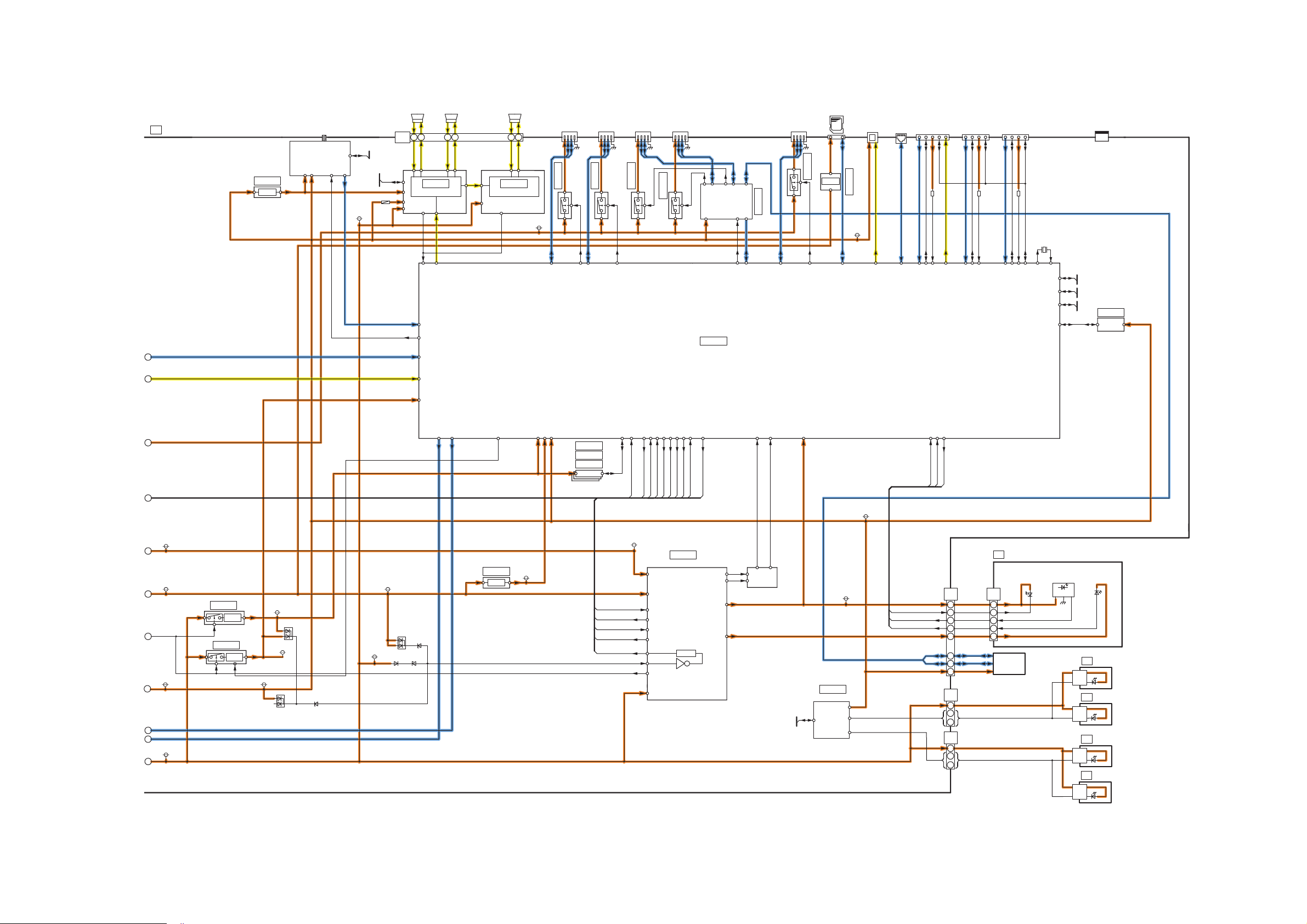
10.3. Block (2/2) Diagram
IC8456
VBUS3
JK8600
SD CARD
+3.3V
SD DATA
SUB3.3V
SD I/F
AUDIO OUT
IC8660
D3201
DIGITAL
IEC_OUT
JK8650A
ETHERNET
ETHER_I/F
JK4702
HDMI2
DDC IIC0
TMDS DATA/
CLOCK
Rx2
DDC2
+5V
HDMI_CEC
ARC_OUT
HDMI_5V_DET2
JK4701
HDMI1
DDC IIC3
TMDS DATA/
CLOCK
Rx3
DDC3
+5V
HDMI_CEC
HDMI_5V_DET3
JK4703
HDMI3
DDC IIC1
TMDS DATA/
CLOCK
Rx1
DDC1
+5V
HDMI_CEC
CEC
HDMI_5V_DET1
X8300
27MHz
IIC_0
IIC_2
IIC_3
NAND_IF
CN0100
IIC_0
IIC_2
IIC_3
FOR
FACTORY
USE
IIC_0
IIC_2
UART
IC8900
NAND
FLASH
SPEAKER_R
A
MAIN
MAIN
TU6706
TUNER
TU_1.8V
TU_3.3V
RF IN
FE_XRST
IIC_2
A12
IIC_0
IF
IC8714
+1.8V
1
2
PA4900
P15V
2
R(-)
15V
SPEAKER_L
1
R(+)
IC4900
AUDIO AMP
SOS
SDIN
AUDIO_OUT
SOUND_SOS_DET
IF
FE_RST
COMPONENT IN
CVBS IN
L/R IN
SUB1.2V
WOOFER
IC8457
WiFi
A20
PWR2
DD2
USB HUB
PWR1
A23
CAMERA
DD3
DD1
IC8458
VBUS0
USB_I/F
USB_I/F
JK8601
4
3
L(-)
L(+)
6
5
W(+)
W(-)
IC4903
AUDIO AMP
15V
SOS
USB1
IC8455
USB5V
USB_I/F
VBUS2
JK8603A
IC8454
USB_I/F
USB3
VBUS1
JK8602
USB2
IC8453
IC8000
Paragon
3
4
5
6
7
8
9
10
11
STB5V
SUB3.3V
LVDS_DATA
P15V
IC8101
IC8100
+1.5V
+1.1V
SUB3.3V
SUB1.5V
SUB1.1V
D5188
D5191
D5187
P15V
LVDS_Tx
P_AFB
SUB1.5V
HDMI3.3V
SUB3.3V
DDR_I/F
BL_SOS
SUB_ON
KEY
PANEL_VCC_ON
POWER_ON
BL_ON
PWM_EN
PANEL_PWM
TV_SOS
PANEL_VCC_
ON_INPUT
XRST
POWER_DET
STB3.3V
CATS_EYE
RM_IN
R_LED_ON
IC8200
IC8201
IC8202
DDR3
PANEL_VCC_
PWM_EN
TV_SOS
P_PWMA
PANEL_VCC_ON
IC5000
LATCH
ON_INPUT
STB3.3V
SUB_AI_3.3V
Paragon
Reset
Circuit
IIC
IC2002
LOGO_LED
STB3.3V
SUB3.3V
R_LED_ON
REMOTE
AI_SENSOR
BL_ON
KEY
BL_SOS
SUB_ON
POWER_ON
STB5V
ANALOG-ASIC
IC8706
AVDDH3.3V
SUB5VSUB5V
D5179
D5178
D5173
D5172
+3.3V
P_PWMA
BL_PWM
PWM_EN
TV_SOS
SUB_ON
OVP
DCDCEN
STB5V
SUB5V
PWM_A_IN
PWM_A_OUT
PWM_POWON
TV_SOS
SUB_ON
OVP_DET
DCDC_CTL
P15V
REMOTE
R_LED_ON
AI_SENSOR
A10
10
11
A05
A06
5
7
1
4
3
9
5
1
4
2
3
6
STB3.3V
R_LED_ON
REMOTE
AI_SENSOR
SUB3.3V
BT_USBDP
BT_USBDN
BT_3.3V
K
POWER LED/REMOTE RECEIVER/C.A.T.S. SENSOR
RM2800
VCC
3
C.A.T.S.
SENSOR
SN2800
OUT
1
2
LL
K10
5
7
1
4
3
DONGLE
BT
POWER LED
D2802A
REMOTE
RECEIVER
LL5
LA
LA5
LR
LR6
LB
LOGO_LED
LOGO_LED
LOGO_LED
LOGO_LED
LB6
30
Page 31
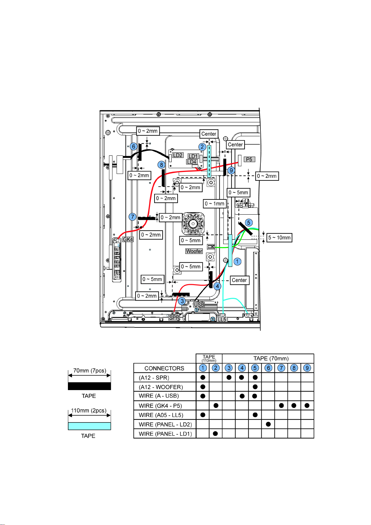
11 Wiring Connection Diagram
11.1. Caution statement.
Caution:
Please confirm that all flexible cables are assembled correctly.
Also make sure that they are locked in the connectors.
Verify by giving the flexible cables a very slight pull.
11.2. Wiring 1
31
Page 32
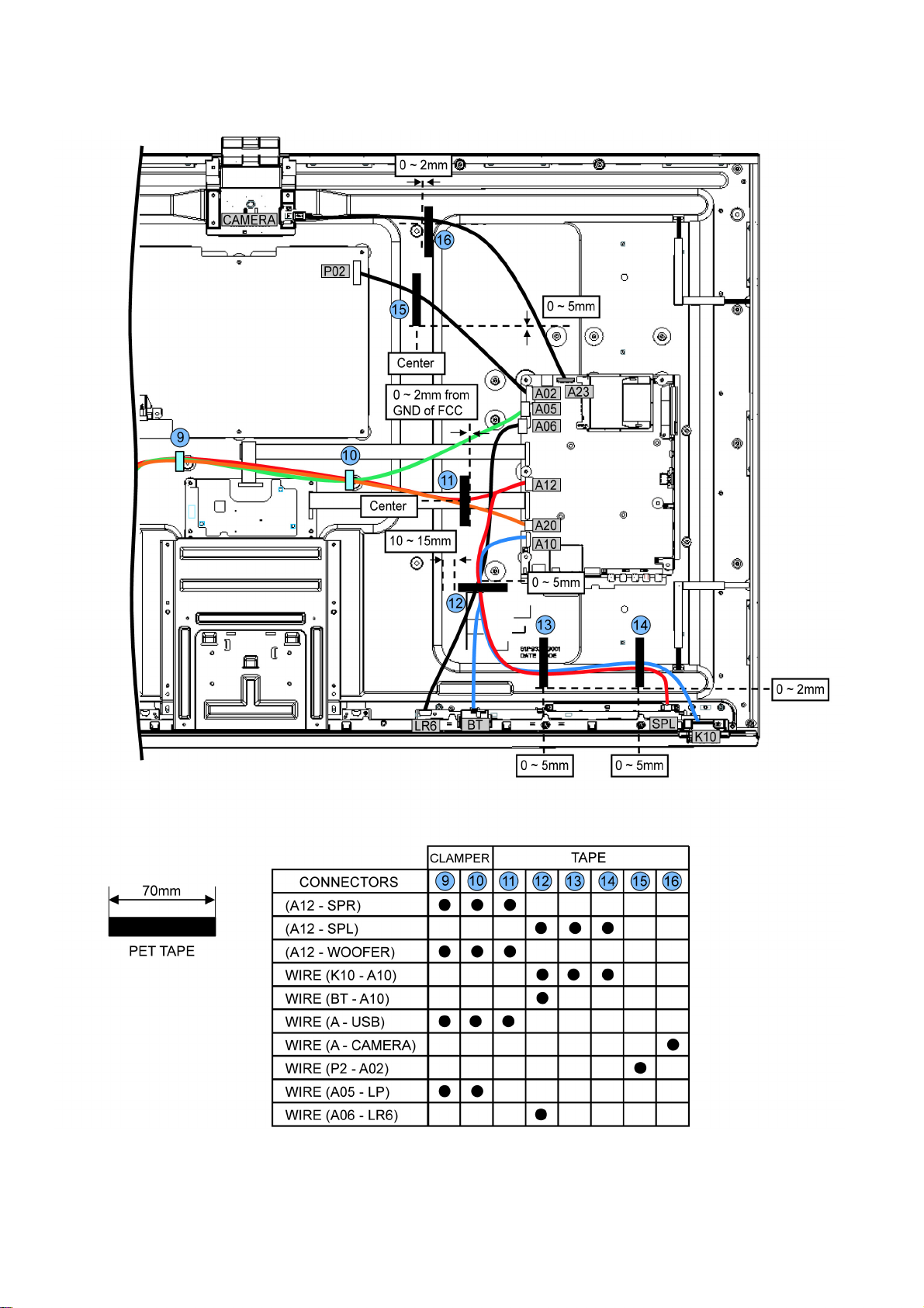
11.3. Wiring 2
32
Page 33
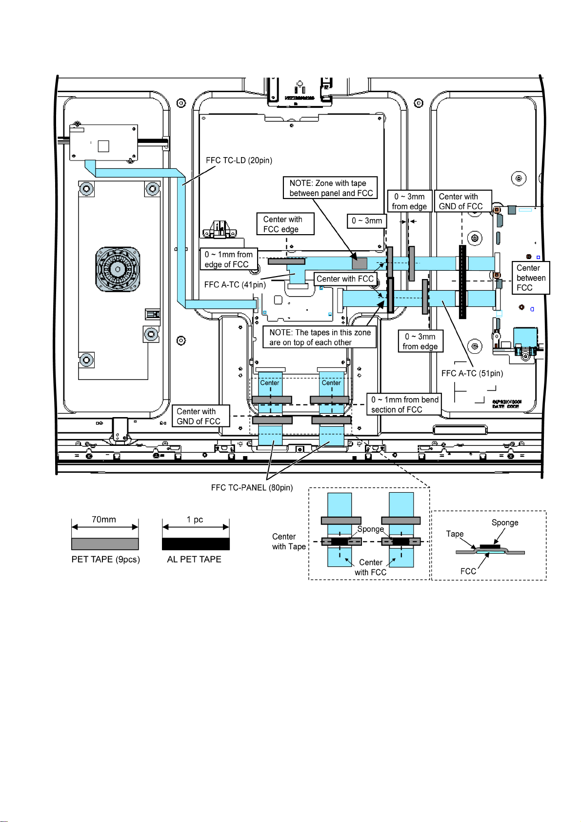
11.4. Wiring 3
33
Page 34
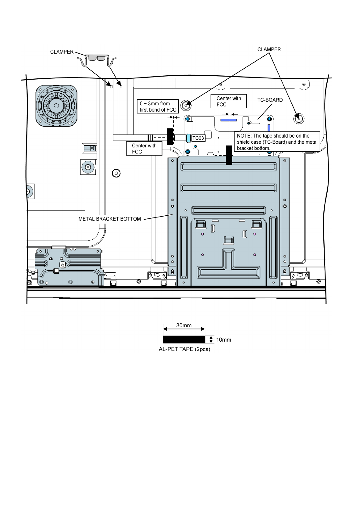
11.5. Wiring 3
34
 Loading...