

Page 1
ORDER NO.MTNC110102CE
B32 Canada: B61
42 inch Class 1080p LCD HDTV
Model No. TC-L42U30
LA14 Chassis
© Panasonic Corporation 2011.
Unauthorized copying and distribution is a violation
of law.
Page 2

TABLE OF CONTENTS
PAG E PAGE
1 Safety Precautions -----------------------------------------------3
1.1. General Guidelines ----------------------------------------3
2 Warning --------------------------------------------------------------4
2.1. Prevention of Electrostatic Discharge (ESD)
to Electrostatically Sensitive (ES) Devices ----------4
2.2. About lead free solder (PbF) ----------------------------5
3 Service Navigation------------------------------------------------6
3.1. PCB Layout --------------------------------------------------6
3.2. Applicable signals ------------------------------------------6
4 Specifications ------------------------------------------------------7
5 Service Mode -------------------------------------------------------8
5.1. How to enter into Service Mode ------------------------8
5.2. SRV-TOOL------------------------------------------------- 10
5.3. Hotel mode------------------------------------------------- 11
5.4. Data Copy by SD Card --------------------------------- 12
6 Troubleshooting Guide---------------------------------------- 15
6.1. Check of the IIC bus lines ------------------------------ 15
6.2. Power LED Blinking timing chart --------------------- 16
6.3. LCD Panel test mode ----------------------------------- 16
7 Disassembly and Assembly Instructions --------------- 17
7.1. Pedestal ---------------------------------------------------- 17
7.2. Rear cover ------------------------------------------------- 17
7.3. AC cord ----------------------------------------------------- 17
7.4. P-Board ----------------------------------------------------- 18
7.5. Side AV bracket------------------------------------------- 18
7.6. A-Board ----------------------------------------------------- 18
7.7. Control panel comp -------------------------------------- 19
7.8. Speaker unit ---------------------------------------------- 19
7.9. Metal bracket right --------------------------------------- 19
7.10. VESA metal and Metal vertical bracket ------------- 19
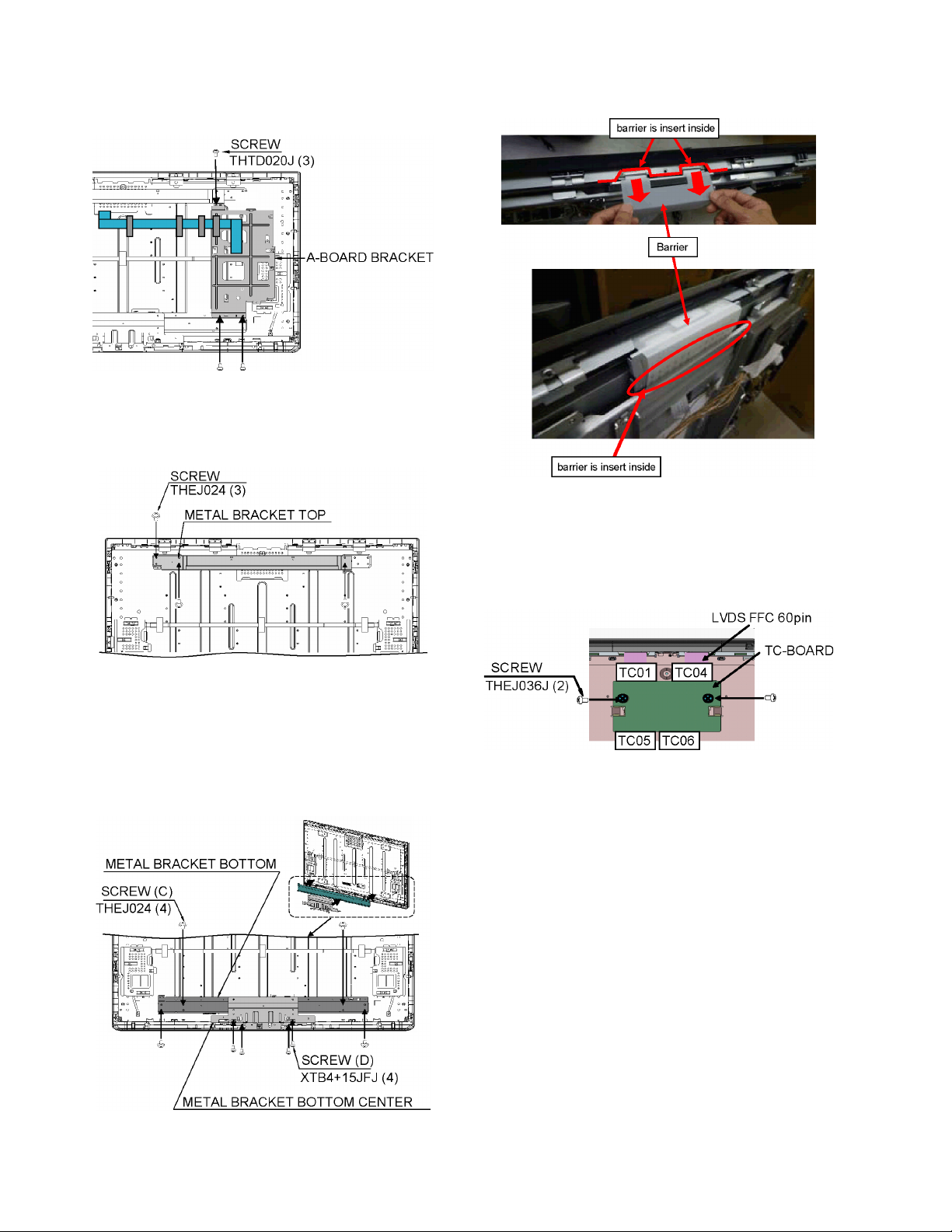
7.11. A-Board bracket ------------------------------------------ 20
7.12. Metal bracket top ----------------------------------------- 20
7.13. Metal bracket bottom and Metal bracket
bottom center---------------------------------------------- 20
7.14. Barrier ------------------------------------------------------- 20
7.15. TC-Board --------------------------------------------------- 20
7.16. LCD Top MTG and LCD side MTG ------------------ 21
7.17. LCD Panel ------------------------------------------------- 21
7.18. KA-Board --------------------------------------------------- 21
7.19. EMI processing ------------------------------------------- 22
8 Measurements and Adjustments -------------------------- 34
8.1. VCOM Adjustment (Flicker Adjustment) ----------- 34
8.2. Voltage chart of A-board-------------------------------- 35
8.3. Picture level adjustment (RF) ------------------------- 35
9 Block Diagram --------------------------------------------------- 37
9.1. Main Block Diagram ------------------------------------- 37
9.2. Block (1/3) Diagram ------------------------------------- 38
9.3. Block (2/3) Diagram ------------------------------------- 39
9.4. Block (3/3) Diagram ------------------------------------- 40
10 Wiring Connection Diagram --------------------------------- 41
10.1. Caution statement. --------------------------------------- 41
10.2. Wiring ------------------------------------------------------- 41
11 Schematic Diagram--------------------------------------------- 43
11.1. Schematic Diagram Note ------------------------------ 43
11.2. Replacement Parts List Note-------------------------- 43
11.3. A-Board (1/8) Schematic Diagram ------------------- 44
11.4. A-Board (2/8) Schematic Diagram ------------------- 45
11.5. A-Board (3/8) Schematic Diagram ------------------- 46
11.6. A-Board (4/8) Schematic Diagram ------------------ 47
11.7. A-Board (5/8) Schematic Diagram ------------------ 48
11.8. A-Board (6/8) Schematic Diagram ------------------ 49
11.9. A-Board (7/8) Schematic Diagram ------------------ 50
11.10. A-Board (8/8) and KA-Board Schematic
Diagram ---------------------------------------------------- 51
11.11. TC-Board (1/3) Schematic Diagram ---------------- 52
11.12. TC-Board (2/3) Schematic Diagram ---------------- 53
11.13. TC-Board (3/3) Schematic Diagram ---------------- 54
12 Printed Circuit Board------------------------------------------ 55
12.1. A-Board ---------------------------------------------------- 55
12.2. KA-Board -------------------------------------------------- 57
12.3. TC-Board -------------------------------------------------- 58
13 Exploded View--------------------------------------------------- 59
13.1. Exploded View-------------------------------------------- 59
13.2. Electrical Replacement Parts List ------------------- 61
2
Page 3
1 Safety Precautions
1.1. General Guidelines
1. When servicing, observe the original lead dress. If a short circuit is found, replace all parts which have been overheated or
damaged by the short circuit.
2. After servicing, see to it that all the protective devices such as insulation barriers, insulation papers shields are properly
installed.
3. After servicing, make the following leakage current checks to prevent the customer from being exposed to shock hazards.
4. When conducting repairs and servicing, do not attempt to modify the equipment, its parts or its materials.
5. When wiring units (with cables, flexible cables or lead wires) are supplied as repair parts and only one wire or some of the
wires have been broken or disconnected, do not attempt to repair or re-wire the units. Replace the entire wiring unit instead.
6. When conducting repairs and servicing, do not twist the Faston connectors but plug them straight in or unplug them straight
out.
1.1.1. Leakage Current Cold Check
1. Unplug the AC cord and connect a jumper between the
two prongs on the plug.
2. Measure the resistance value, with an ohmmeter,
between the jumpered AC plug and each exposed metallic cabinet part on the equipment such as screwheads,
connectors, control shafts, etc. When the exposed metallic part has a return path to the chassis, the reading
should be 100 Mohm and over.
When the exposed metal does not have a return path to
the chassis, the reading must be .
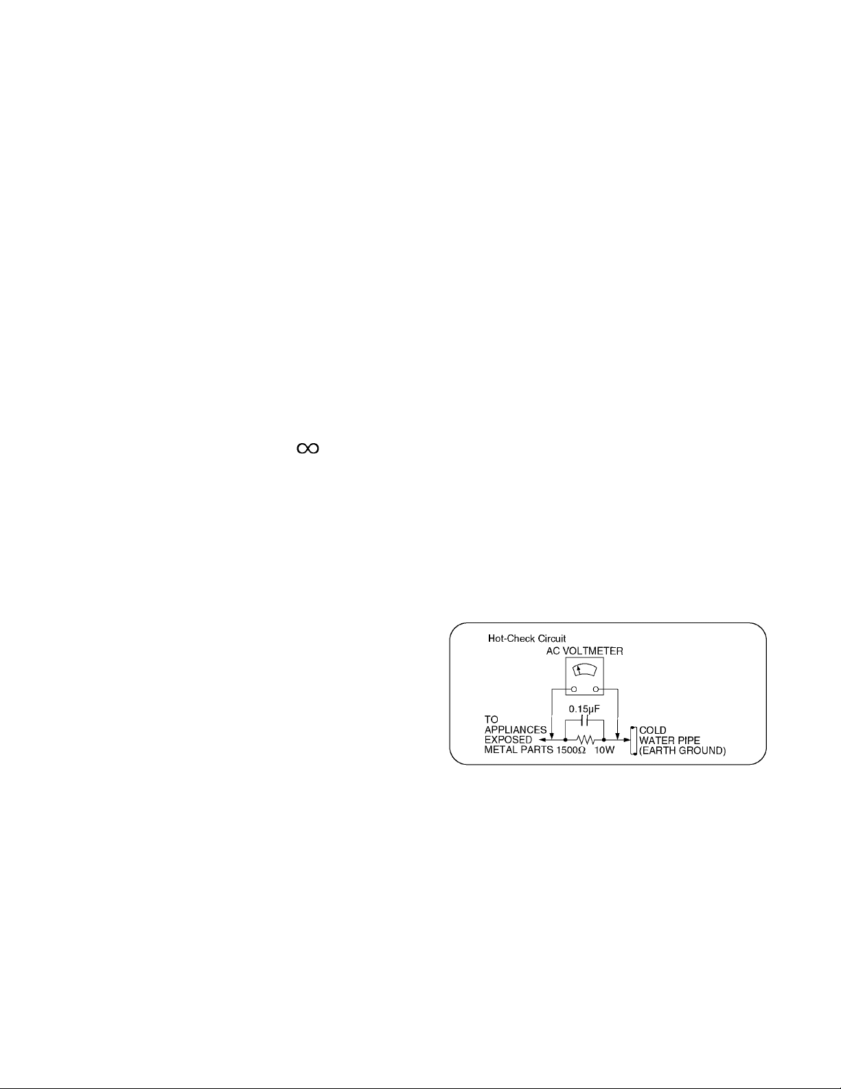
1.1.2. Leakage Current Hot Check (See Figure 1.)
1. Plug the AC cord directly into the AC outlet. Do not use
an isolation transformer for this check.
2. Connect a 1.5kohm, 10 watts resistor, in parallel with a
0.15μF capacitors, between each exposed metallic part
on the set and a good earth ground such as a water pipe,
as shown in Figure 1.
3. Use an AC voltmeter, with 1000 ohms/volt or more sensitivity, to measure the potential across the resistor.
4. Check each exposed metallic part, and measure the voltage at each point.
5. Reverse the AC plug in the AC outlet and repeat each of
the above measurements.
6. The potential at any point should not exceed 0.75 volts
RMS. A leakage current tester (Simpson Model 229 or
equivalent) may be used to make the hot checks, leakage
current must not exceed 1/2 milliamp. In case a measurement is outside of the limits specified, there is a possibility
of a shock hazard, and the equipment should be repaired
and rechecked before it is returned to the customer.
Figure 1
3
Page 4

2 Warning
2.1. Prevention of Electrostatic Discharge (ESD) to Electrostatically Sensitive (ES) Devices
Some semiconductor (solid state) devices can be damaged easily by static electricity. Such components commonly are called Electrostatically Sensitive (ES) Devices. Examples of typical ES devices are integrated circuits and some field-effect transistors and
semiconductor [chip] components. The following techniques should be used to help reduce the incidence of component damage
caused by electrostatic discharge (ESD).
1. Immediately before handling any semiconductor component or semiconductor-equipped assembly, drain off any ESD on your
body by touching a known earth ground. Alternatively, obtain and wear a commercially available discharging ESD wrist strap,
which should be removed for potential shock reasons prior to applying power to the unit under test.
2. After removing an electrical assembly equipped with ES devices, place the assembly on a conductive surface such as aluminum foil, to prevent electrostatic charge buildup or exposure of the assembly.
3. Use only a grounded-tip soldering iron to solder or unsolder ES devices.
4. Use only an anti-static solder removal device. Some solder removal devices not classified as [anti-static (ESD protected)] can
generate electrical charge sufficient to damage ES devices.
5. Do not use freon-propelled chemicals. These can generate electrical charges sufficient to damage ES devices.
6. Do not remove a replacement ES device from its protective package until immediately before you are ready to install it. (Most
replacement ES devices are packaged with leads electrically shorted together by conductive foam, aluminum foil or comparable conductive material).
7. Immediately before removing the protective material from the leads of a replacement ES device, touch the protective material
to the chassis or circuit assembly into which the device will be installed.
Caution
Be sure no power is applied to the chassis or circuit, and observe all other safety precautions.
8. Minimize bodily motions when handling unpackaged replacement ES devices. (Otherwise ham less motion such as the brushing together of your clothes fabric or the lifting of your foot from a carpeted floor can generate static electricity (ESD) sufficient
to damage an ES device).
4
Page 5
2.2. About lead free solder (PbF)
Note: Lead is listed as (Pb) in the periodic table of elements.
In the information below, Pb will refer to Lead solder, and PbF will refer to Lead Free Solder.
The Lead Free Solder used in our manufacturing process and discussed below is (Sn+Ag+Cu).
That is Tin (Sn), Silver (Ag) and Copper (Cu) although other types are available.
This model uses Pb Free solder in it’s manufacture due to environmental conservation issues. For service and repair work, we’d
suggest the use of Pb free solder as well, although Pb solder may be used.
PCBs manufactured using lead free solder will have the PbF within a leaf Symbol PbF stamped on the back of PCB.
Caution
• Pb free solder has a higher melting point than standard solder. Typically the melting point is 50 ~ 70 °F (30~40 °C) higher. Please
use a high temperature soldering iron and set it to 700 ± 20 °F (370 ± 10 °C).
• Pb free solder will tend to splash when heated too high (about 1100 °F or 600 °C).
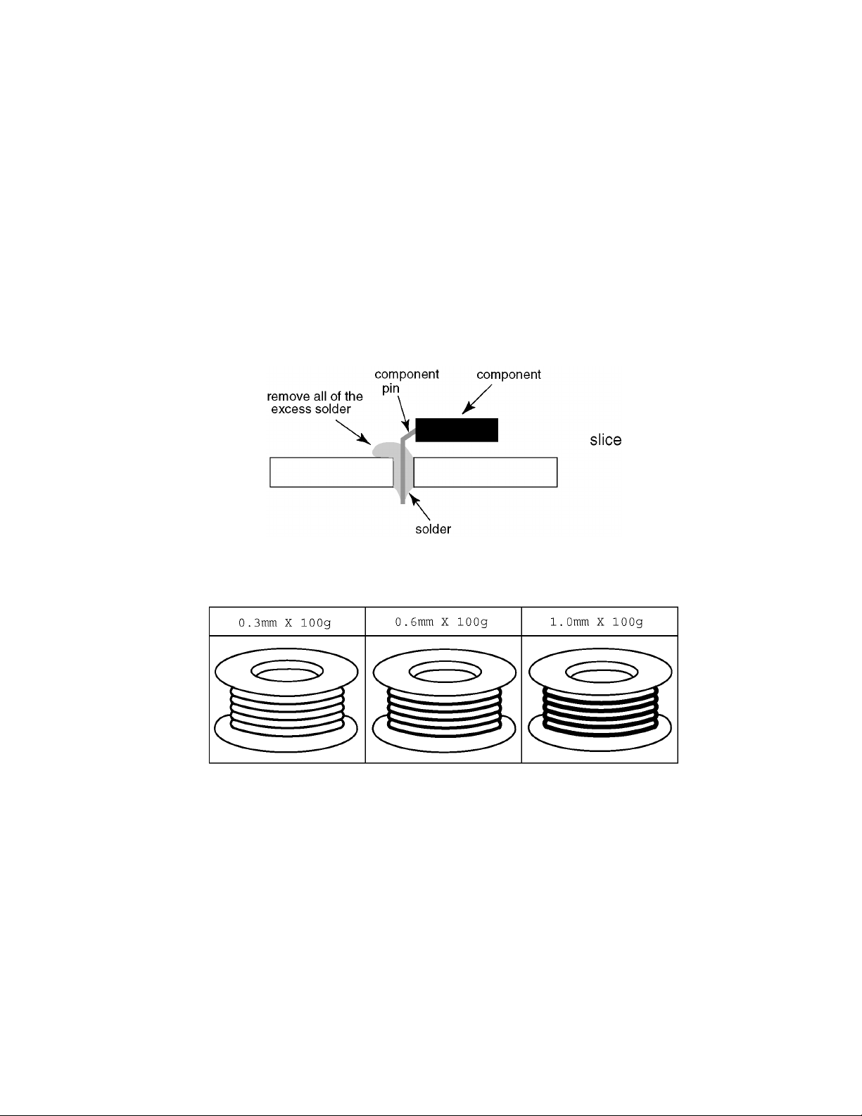
If you must use Pb solder, please completely remove all of the Pb free solder on the pins or solder area before applying Pb solder. If this is not practical, be sure to heat the Pb free solder until it melts, before applying Pb solder.
• After applying PbF solder to double layered boards, please check the component side for excess solder which may flow onto the
opposite side. (see figure below)
Suggested Pb free solder
There are several kinds of Pb free solder available for purchase. This product uses Sn+Ag+Cu (tin, silver, copper) solder. However, Sn+Cu (tin, copper), Sn+Zn+Bi (tin, zinc, bismuth) solder can also be used.
5
Page 6
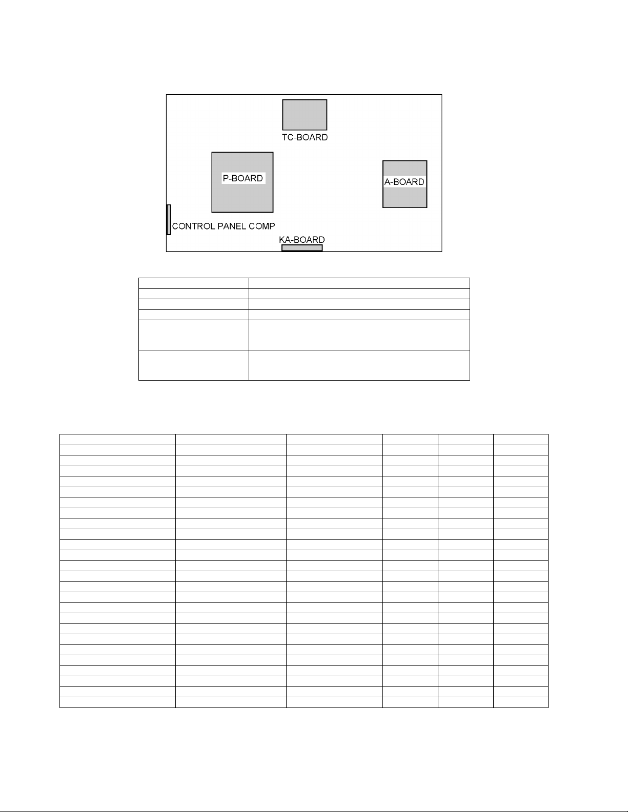
3 Service Navigation
3.1. PCB Layout
Board Name Function
A-Board Main
TC-Board Tcon, Double Speed
KA-Board Remote Receiver, LED, Cat’s eye
P-Board Power Supply
Control Panel Comp Control Panel
Non serviceable
P-Board should be exchanged for service.
Non serviceable
Control Panel Comp should be exchanged for service.
3.2. Applicable signals
* Mark: Applicable input signal for Component (Y, PB, PR), HDMI and PC
horizontal frequency (kHz) vertical frequency (Hz) COMPONENT HDMI PC
525 (480) / 60i 15.73 59.94 * *
525 (480) /60p 31.47 59.94 * *
750 (720) /60p 45.00 59.94 * *
1,125 (1,080) /60i 33.75 59.94 * *
1,125 (1,080) /60p 67.43 59.94 *
1,125 (1,080) /60p 67.50 60.00 *
1,125 (1,080) /24p 26.97 23.98 *
1,125 (1,080) /24p 27.00 24.00 *
640 × 400 @70 31.47 70.08 *
640 × 480 @60 31.47 59.94 *
Macintosh13 inch (640 × 480) 35.00 66.67 *
640 × 480 @75 37.50 75.00 *
852 × 480 @60 31.44 59.89 *
800 × 600 @60 37.88 60.32 *
800 × 600 @75 46.88 75.00 *
800 × 600 @85 53.67 85.08 *
Macintosh16 inch (832 × 624) 49.73 74.55 *
1,024 × 768 @60 48.36 60.00 *
1,024 × 768 @70 56.48 70.07 *
1,024 × 768 @75 60.02 75.03 *
1,024 × 768 @85 68.68 85.00 *
Macintosh 21 inch (1,152 ×870) 68.68 75.06 *
1,280 × 768 @60 47.78 59.87 *
1,280 × 1,024 @60 63.98 60.02 *
1,366 × 768 @60 48.39 60.04 *
Note
• Signals other than above may not be displayed properly.
• The above signals are reformatted for optimal viewing on your display.
6
Page 7

4 Specifications
Power Source AC 110-127 V, 60 Hz
Power Consumption
Rated Power Consumption 210 W
Standby Condition 0.3 W
Display panel
Aspect Ratio 16:9
Visible screen size 42 inch class (42.0 inches measured diagonally)
(W × H × Diagonal) 36.6 inch × 20.6 inch × 42.0 inch (930 mm × 523 mm × 1,067 mm)
(No. of pixels) 2,073,600 (1,920 (W) × 1,080 (H)) [5,760 × 1,080 dots]
Sound
Speaker 1-way 2 bottom SP System
Audio Output 20 W [10 W + 10 W] ( 10 % THD )
PC signals VGA, SVGA, XGA, WXGA, SXGA
Channel CapabilityATSC/NTSC (Digital/Analog)
Operating Conditions Temperature: 32 °F - 95 °F (0 °C - 35°C)
Connection Terminals
VIDEO IN 1-2 VIDEO: RCA PIN Type × 1 1.0 V [p-p] (75 Ω)
COMPONENT IN Y: 1.0 V [p-p] (including synchronization)
HDMI 1-3 TYPE A Connector × 3.
PC D-SUB 15PIN: R,G,B / 0.7 V [p-p] (75 Ω)
Card slot SD CARD slot × 1
DIGITAL AUDIO OUT PCM / Dolby Digital, Fiber Optic
FEATURES 3D Y/C FILTER, CLOSED CAPTION,
Dimensions (W × H × D)
Including TV stand 40.2 inch × 26.3 inch × 11.4 inch (1,021 mm
TV Set only 40.2 inch × 24.9 inch × 4.3 inch (1,021 mm × 632 mm × 107 mm)
Mass
Including TV stand 42.0 lb. (19.0 kg) NET
TV Set only 37.5 lb. (17.0 kg) NET
Horizontal scanning frequency 31 - 69 kHz
Vertical scanning frequency 59 - 86 Hz
VHF/ UHF: 2 - 69, CATV: 1 - 135
Humidity: 20 % - 80 % RH (non-condensing)
AUDIO L - R: RCA PIN Type × 2 0.5 V [rms]
PB, PR: ±0.35 V [p-p]
AUDIO L-R: RCA PIN Type × 2 0.5 V [rms]
O This TV supports [HDAVI Control 5] function.
HD, VD / 1.0 - 5.0 V [p-p] (high impedance)
V-Chip, HDAVI Control 5
Vesa compatible, VIERA IMAGE VIEWER
× 666 mm × 288 mm)
Note
• Design and Specifications are subject to change without notice. Mass and Dimensions shown are approximate.
7
Page 8
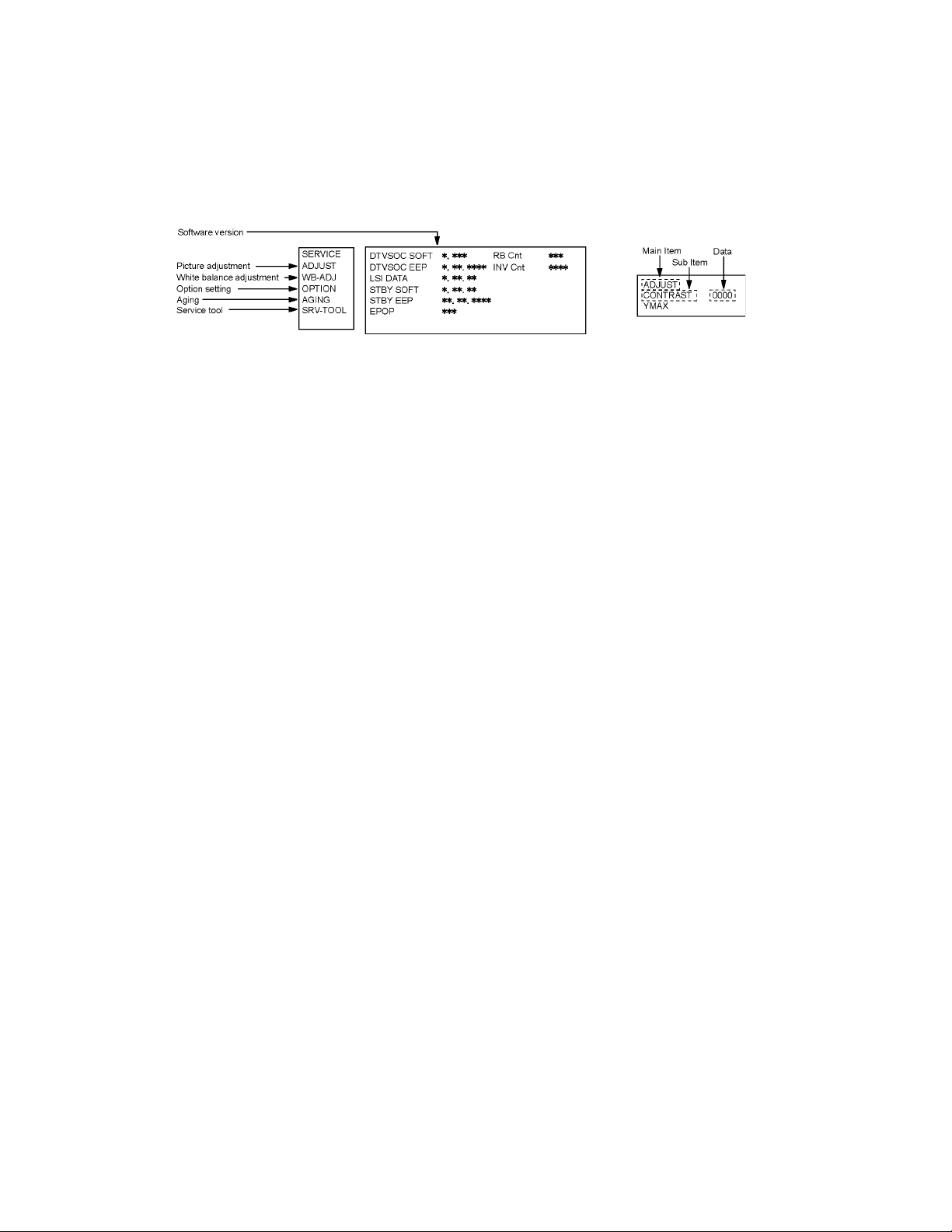
5 Service Mode
5.1. How to enter into Service Mode
5.1.1. Purpose
After exchange parts, check and adjust the contents of adjustment mode.
While pressing [VOLUME ( - )] button of the main unit, press [INFO] button of the remote control three times within 2 seconds.
5.1.2. Key command
[1] button...Main items Selection in forward direction
[2] button...Main items Selection in reverse direction
[3] button...Sub items Selection in forward direction
[4] button...Sub items Selection in reverse direction
[VOL] button...Value of sub items change in forward direction ( + ), in reverse direction ( - )
5.1.3. How to exit
Switch off the power with the [POWER] button on the main unit or the [POWER] button on the remote control.
8
Page 9
5.1.4. Contents of adjustment mode
• Value is shown as a hexadecimal number.
• Preset value differs depending on models.
• After entering the adjustment mode, take note of the value in each item before starting adjustment.
Main item Sub item Sample Data Remark
ADJUST CONTRAST 2E
COLOR 00
TINT 00
SUB-BRT 000
BACKLGT 91EB
V COM 171
WB-ADJ R-GAIN FF
G-GAIN FC
B-GAIN AE
R-CENT 4B
G-CENT 80
B-CENT DF
OPTION Boot ROM Factory Preset.
STBY-SET -EMERGENCY ON
CLK MODE OFF
CLOCK FC8
EDID-CLK HIGH
AGING COUNT Built-in test patterns can be
ALL WHITE
ALL BLACK
ALL RED
ALL GREEN
ALL_BLUE
RASTER1
RASTER2
RASTER3
RASTER4
4DIN1
4DIN2
GRAY WHITE
GRAY RED
GRAY GREEN
GRAY BLUE
FLICKER0
GS1
1 PIX STRIPE
2 PIX STRIPE
1 LINE_STRIPE
COLORBAR
WIDHT COLORBAR
OUTER
LIGHT CHECK
FLICKER1
FLICKER2
FLICKER3
SRV-TOOL 00 See next.
displayed.
9
Page 10
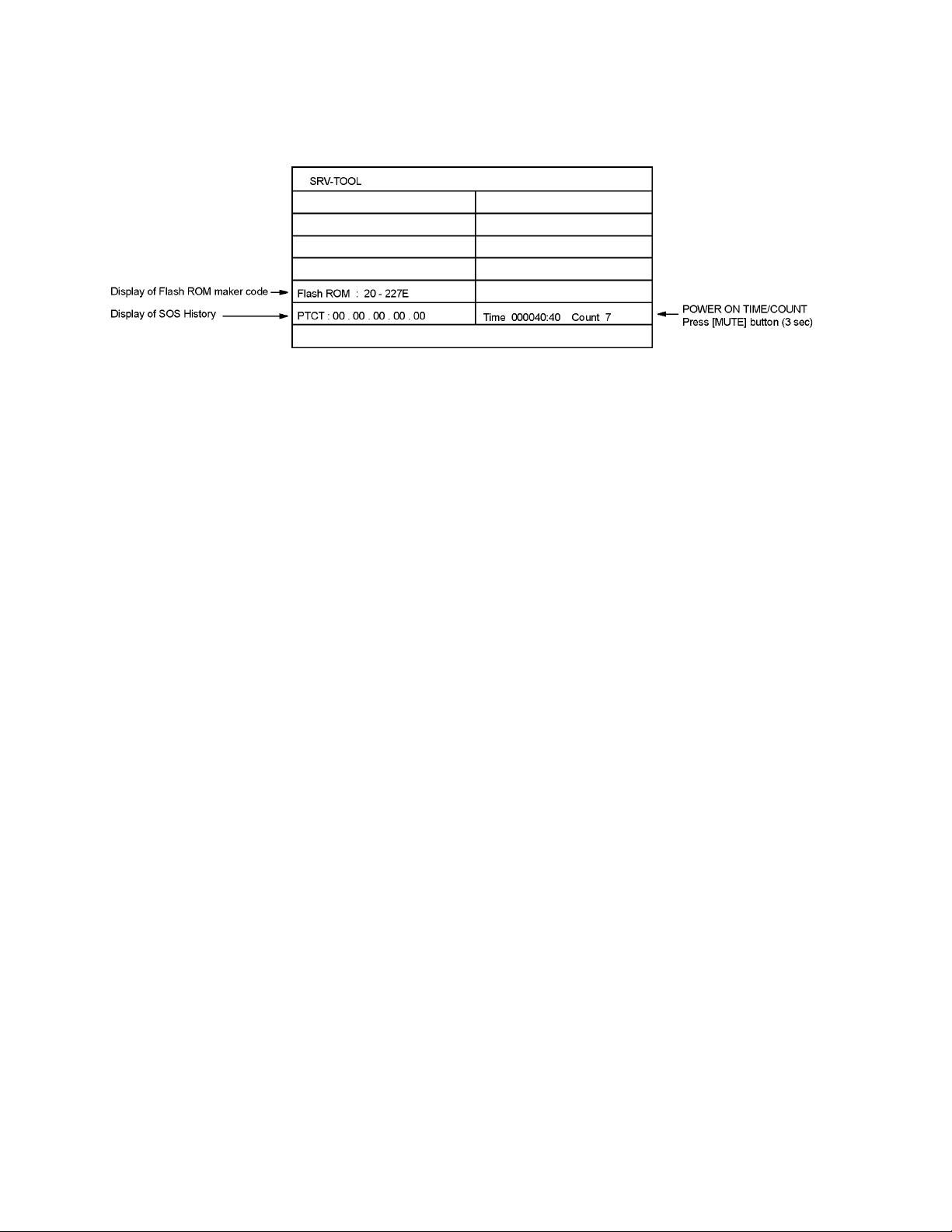
5.2. SRV-TOOL
5.2.1. How to access
1. Select [SRV-TOOL] in Service Mode.
2. Press [OK] button on the remote control.
5.2.2. Display of SOS History
SOS History (Number of LED blinking) indication.
From left side; Last SOS, before Last, three occurrence before, 2nd occurrence after shipment, 1st occurrence after shipment.
This indication except 2nd and 1st occurrence after shipment will be cleared by [Self-check indication and forced to factory shipment setting].
5.2.3. POWER ON TIME/COUNT
Note : To display TIME/COUNT menu, highlight position, then press MUTE for 3 sec.
Time : Cumulative power on time, indicated hour : minute by decimal
Count : Number of ON times by decimal
Note : This indication will not be cleared by either of the self-checks or any other command.
5.2.4. Exit
1. Disconnect the AC cord from wall outlet.
10
Page 11
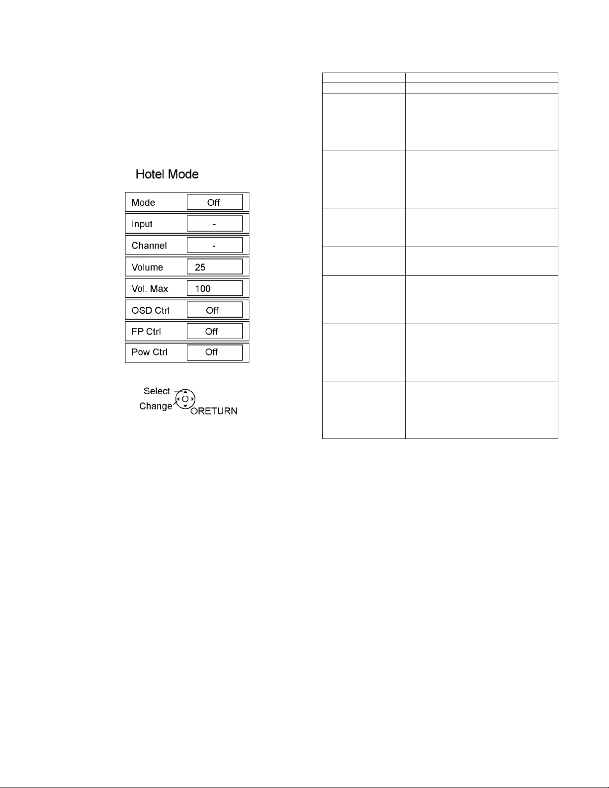
5.3. Hotel mode
1. Purpose
Restrict a function for hotels.
2. Access command to the Hotel mode setup menu
In order to display the Hotel mode setup menu:
While pressing [VOLUME (-)] button of the main unit,
press [INPUT] button of the remote control three times
within 2 seconds.
Then, the Hotel mode setup menu is displayed.
3. To exit the Hotel mode setup menu
Disconnect AC power cord from wall outlet.
4. Explain the Hotel mode setup menu
Item Function
Mode Select hotel mode off/on
Input Select input signal modes.
Set the input, when each time power is
switched on.
Selection:
-/RF/HDMI1/HDMI2/HDMI3/Comp./Video/PC
• OFF: give priority to a last memory.
Channel Select channel when input signal is RF.
Set the channel, each time power is switched
on.
Selection:
Any channel number or [-].
[-] means the channel when turns off.
Volume Adjust the volume when each time power is
switched on.
Range:
0 to 100
Vol. Max Adjust maximum volume.
Range:
0 to 100
OSD Ctrl Restrict the OSD.
Selection:
OFF/PATTERN1
• OFF: No restriction
• PATTERN1: restriction
FP Ctrl Select front key conditions.
Selection:
OFF/ALL/PATTERN1
• OFF: altogether valid.
• ALL: altogether invalid.
• PATTERN1: only input key is valid.
Pow Ctrl Select POWER-ON/OFF condition when AC
power cord is disconnected and then connected.
OFF: The same condition when AC power
cord is disconnected.
ON: Forced power ON condition.
11
Page 12
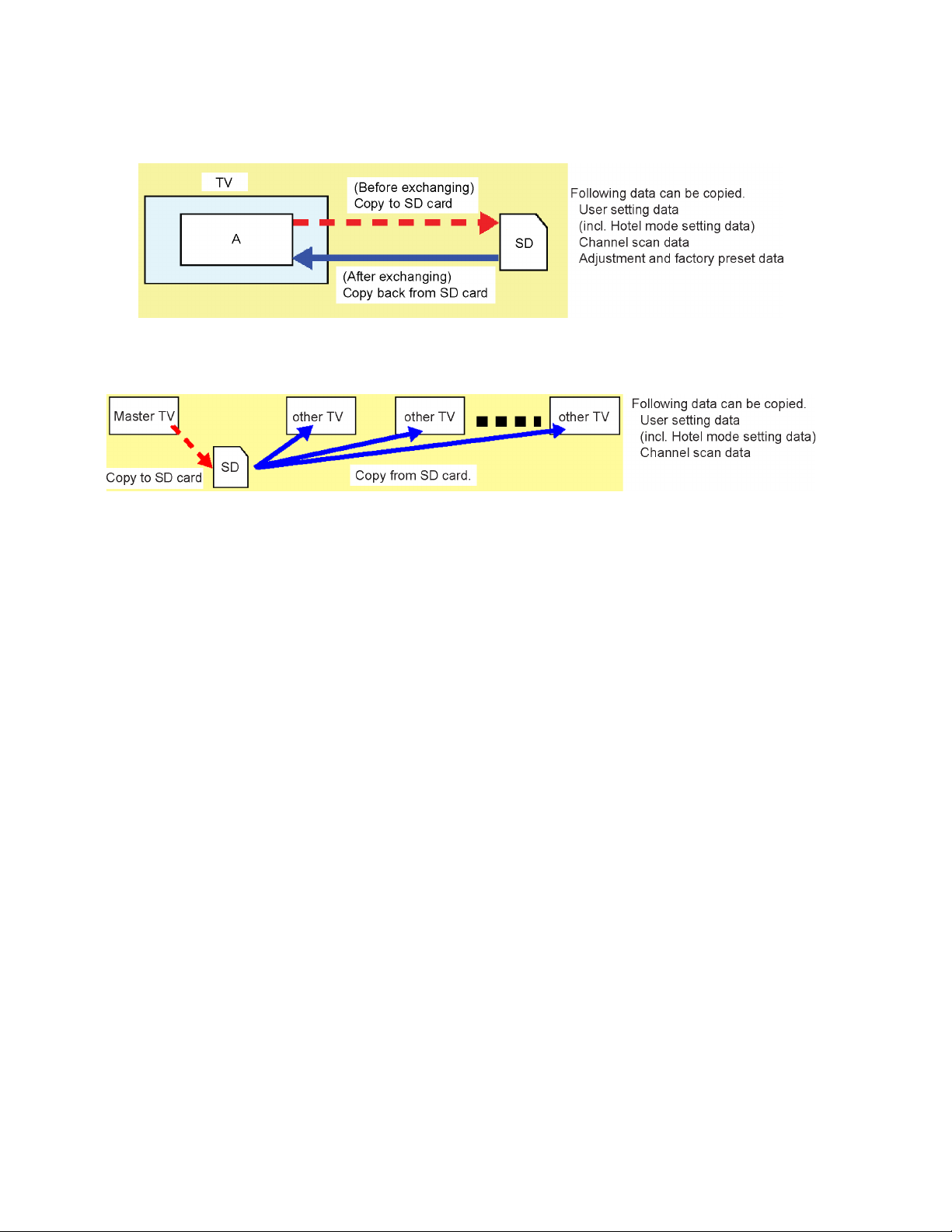
5.4. Data Copy by SD Card
5.4.1. Purpose
(a) Board replacement (Copy the data when exchanging A-board):
When exchanging A-board, the data in original A-board can be copied to SD card and then copy to new A-board.
(b) Hotel (Copy the data when installing a number of units in hotel or any facility):
When installing a number of units in hotel or any facility, the data in master TV can be copied to SD card and then copy to other
TVs.
5.4.2. Preparation
Make pwd file as startup file for (a) or (b) in a empty SD card.
1. Insert a empty SD card to your PC.
2. Right-click a blank area in a SD card window, point to New, and then click text document. A new file is created by default
(New Text Document.txt).
3. Right-click the new text document that you just created and select rename, and then change the name and extension of the
file to the following file name for (a) or (b) and press ENTER.
File name:
(a) For Board replacement : boardreplace.pwd
(b) For Hotel : hotel.pwd
Note:
Please make only one file to prevent the operation error.
No any other file should not be in SD card.
12
Page 13
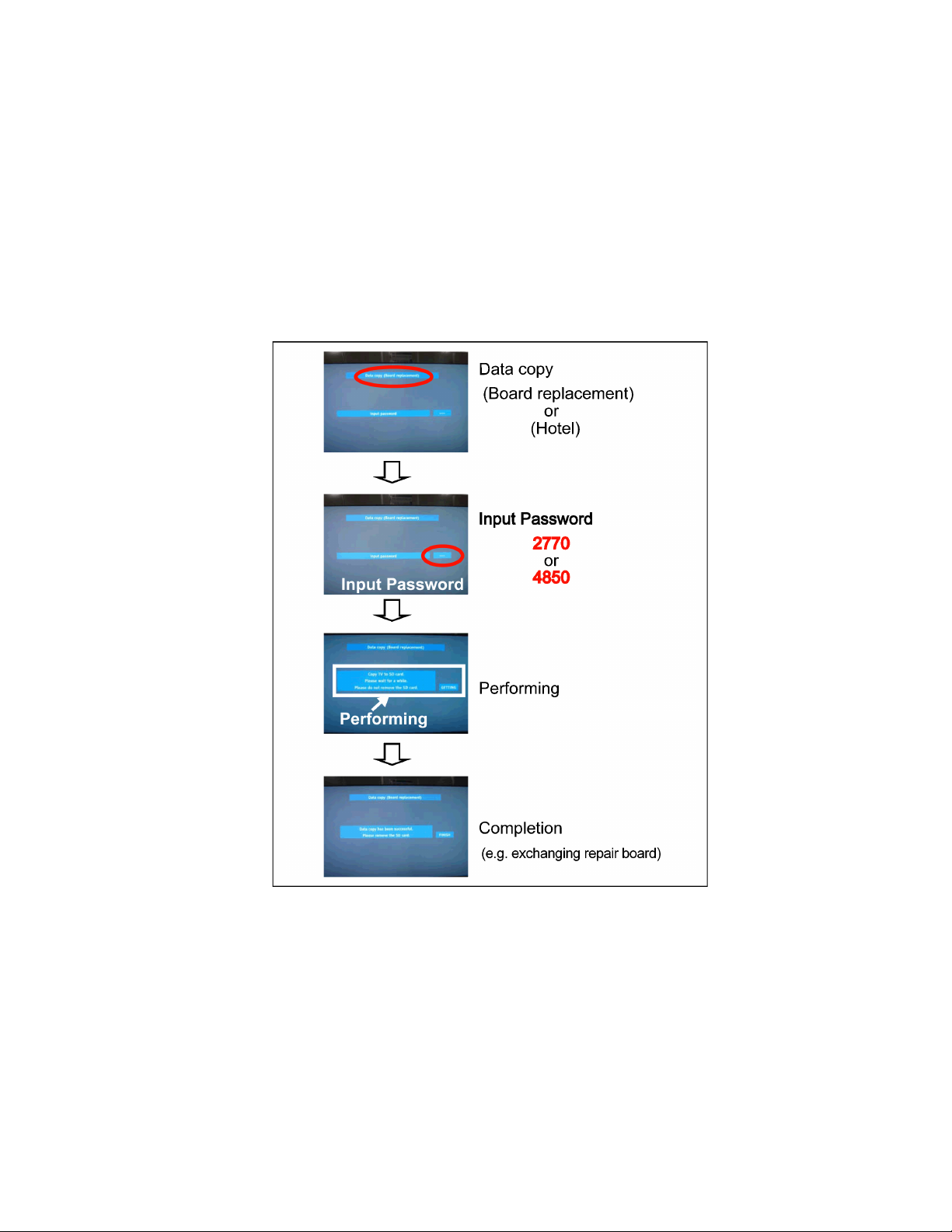
5.4.3. Data copy from TV set to SD Card
1. Turn on the TV set.
2. Insert SD card with a startup file (pwd file) to SD slot.
On-screen Display will be appeared according to the startup file automatically.
3. Input a following password for (a) or (b) by using remote control.
(a) For Board replacement : 2770
(b) For Hotel : 4850
Data will be copied from TV set to SD card.
It takes around 2 to 6 minutes maximum for copying.
4. After the completion of copying to SD card, remove SD card from TV set.
5. Turn off the TV set.
Note:
Following new folder will be created in SD card for data from TV set.
(a) For Board replacement : user_setup
(b) For Hotel : hotel
13
Page 14
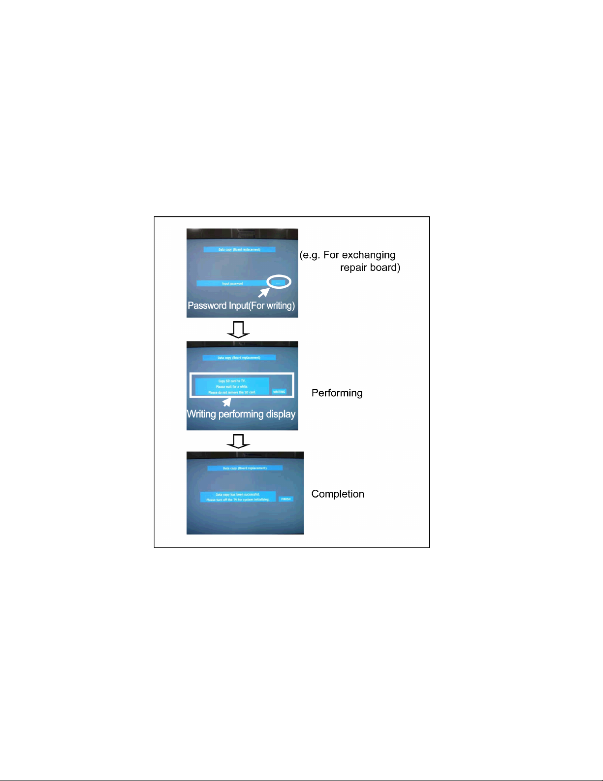
5.4.4. Data copy from SD Card to TV set
1. Turn on the TV set.
2. Insert SD card with Data to SD slot.
On-screen Display will be appeared according to the Data folder automatically.
3. Input a following password for (a) or (b) by using remote control.
(a) For Board replacement : 2771
(b) For Hotel : 4851
Data will be copied from SD card to TV set.
4. After the completion of copying to SD card, remove SD card from TV set.
(a) For Board replacement : Data will be deleted after copying (Limited one copy).
(b) For Hotel : Data will not be deleted and can be used for other TVs.
5. Turn off the TV set.
Note:
1. Depending on the failure of boards, function of Data copy for board replacement does not work.
2. This function can be effective among the same model numbers.
14
Page 15
6 Troubleshooting Guide
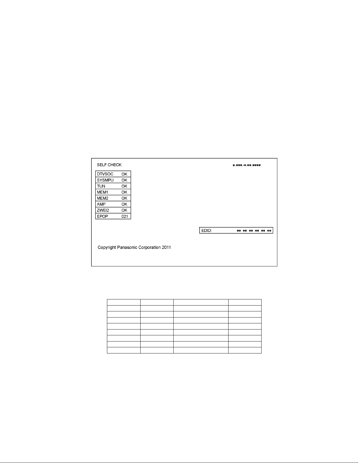
Use the self-check function to test the unit.
1. Checking the IIC bus lines
2. Power LED Blinking timing
6.1. Check of the IIC bus lines
6.1.1. How to access
Self-check indication only:
Produce TV reception screen, and while pressing [VOLUME ( - )] button on the main unit, press [OK] button on the remote control
for more than 3 seconds.
Self-check indication and forced to factory shipment setting:
Produce TV reception screen, and while pressing [VOLUME ( - )] button on the main unit, press [MENU] button on the remote con-
trol for more than 3 seconds.
6.1.2. Exit
Disconnect the AC cord from wall outlet.
6.1.3. Screen display
6.1.4. Check Point
Confirm the following parts if NG was displayed.
DISPLAY Check Ref. No. Description Check Point
DTVSOC IC8001 Nile-TCON A-Board
SYSMPU IC8001 MPU (Nile-TCON) A-Board
TUN TU8302 TUNER A-Board
MEM1 IC8503 EEPROM (Nile-TCON) A-Board
MEM2 IC8004 EEPROM (SYSMPU) A-Board
AMP IC2106 AUDIO AMP A-Board
ZWEI2 IC9006 ZWEI2 TC-Board
EPOP
15
Page 16
6.2. Power LED Blinking timing chart
1. Subject
Information of LED Flashing timing chart.
2. Contents
When an abnormality has occurred the unit, the protection circuit operates and reset to the stand by mode. At this time, the
defective block can be identified by the number of blinks of the Power LED on the front panel of the unit.
Blinking Times Contents Check point
1 BACK LIGHT SOS LCD PANEL
2 SUB 1.8V SOS A-Board
3 SUB 1.2V SOS A-Board
4 POWER SOS A-Board
9 ZWEI2 SOS TC-Board
10 SUB 3.3V SENSE A-Board
12 SOUND SOS A-Board
P-Board
P-Board
Speaker
6.3. LCD Panel test mode
Purpose:
To find the possible failure point where in LCD Panel or Printed Circuit Board when the abnormal picture is displayed.
How to Enter:
While pressing [VOLUME ( - )] button of the main unit, press [SUB MENU] button of the remote control three times within 2
seconds.
How to Exit:
Disconnect AC plug from wall outlet.
How to confirm:
If the abnormal picture is displayed, go into LCD Panel test mode to display the several test patterns.
And then, judge by the following method.
Still abnormal picture is displayed: The cause must be in LCD Panel or TC board.
Normal picture is displayed: The cause must be in A board.
Remarks:
The test pattern is created by the circuit in TC board.
In LCD Panel test mode, this test pattern is displayed unaffected by signal processing for RF or input signal.
If the normal picture is displayed, LCD Panel or TC board must be okay and the cause of failure must be in A board.
16
Page 17
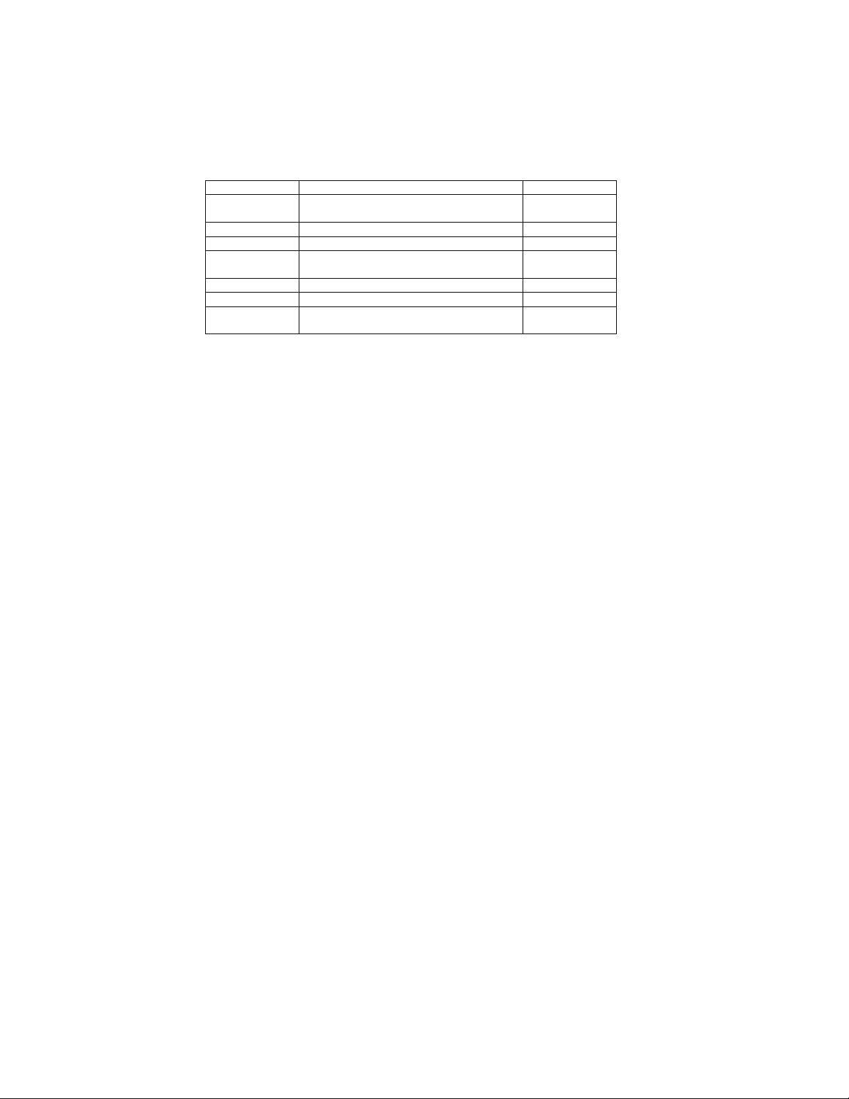
7 Disassembly and Assembly Instructions
7.1. Pedestal
1. Lay down the unit so that the rear cover faces upward.
2. Remove the 4 screws.
3. Remove the pedestal.
7.2. Rear cover
1. Remove the 16 screws (A).
2. Remove the 1 screw (B).
3. Remove the rear cover.
7.3. AC cord
1. Remove the screw and Remove the AC cord bracket.
2. Remove the bushing of the AC cord from the AC cord
bracket.
3. Disconnect the connector (P1) of AC cord.
17
Page 18
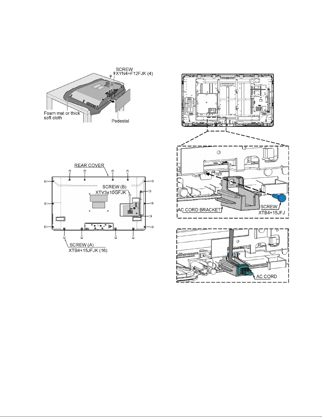
7.4. P-Board
1. Remove the 6 screws.
2. Disconnect the connectors (P1, P2, P3 and P4).
3. Remove the P-Board.
7.5. Side AV bracket
1. Remove the side AV bracket.
7.6. A-Board
1. Remove the 5 screws.
2. Disconnect the connector (A03, A04, A10, A11 and A21).
3. Remove the A-Board.
18
Page 19
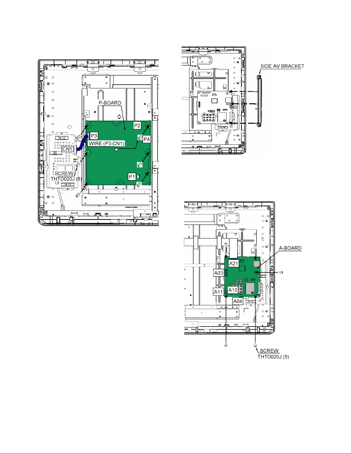
7.7. Control panel comp
1. Disconnect the connector (K1).
2. Remove the 2 screws.
3. Remove the control panel comp.
7.9. Metal bracket right
1. Remove the 2 screws.
2. Remove the Metal bracket right.
7.8. Speaker unit
1. Remove the 4 screws.
2. Remove the speaker unit.
7.10. VESA metal and Metal vertical bracket
1. Remove the 10 screws.
2. Remove the VESA metal and Metal vertical bracket.
19
Page 20
7.11. A-Board bracket
1. Remove the 3 screws.
2. Remove the A-Board bracket.
7.12. Metal bracket top
1. Remove the 3 screws.
2. Remove the Metal bracket top.
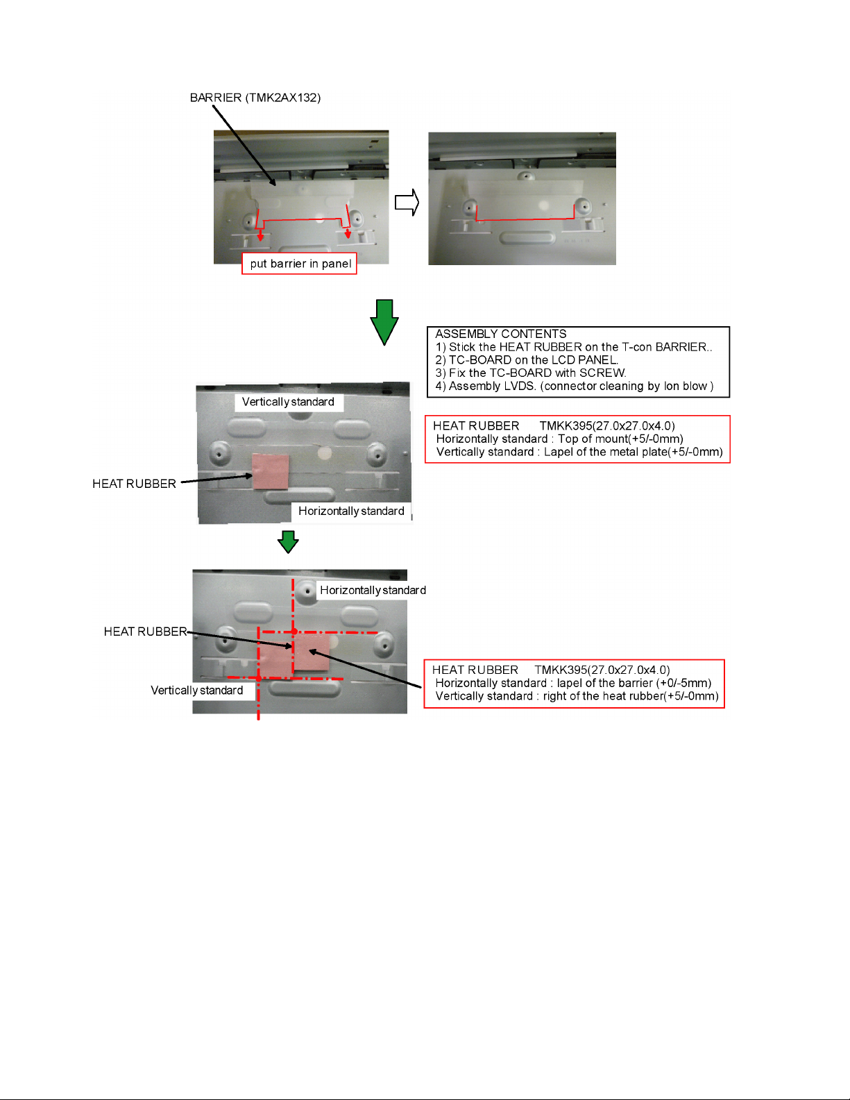
7.14. Barrier
1. Remove the barrier.
7.15. TC-Board
1. Disconnect the connector (TC01, TC04, TC05 and
TC06).
2. Remove the 2 screws.
3. Remove the TC-Board.
7.13. Metal bracket bottom and Metal bracket bottom center
1. Remove the 4 screws (C).
2. Remove the 4 screws (D).
3. Remove the Metal bracket bottom and Metal bracket bottom center.
20
Page 21
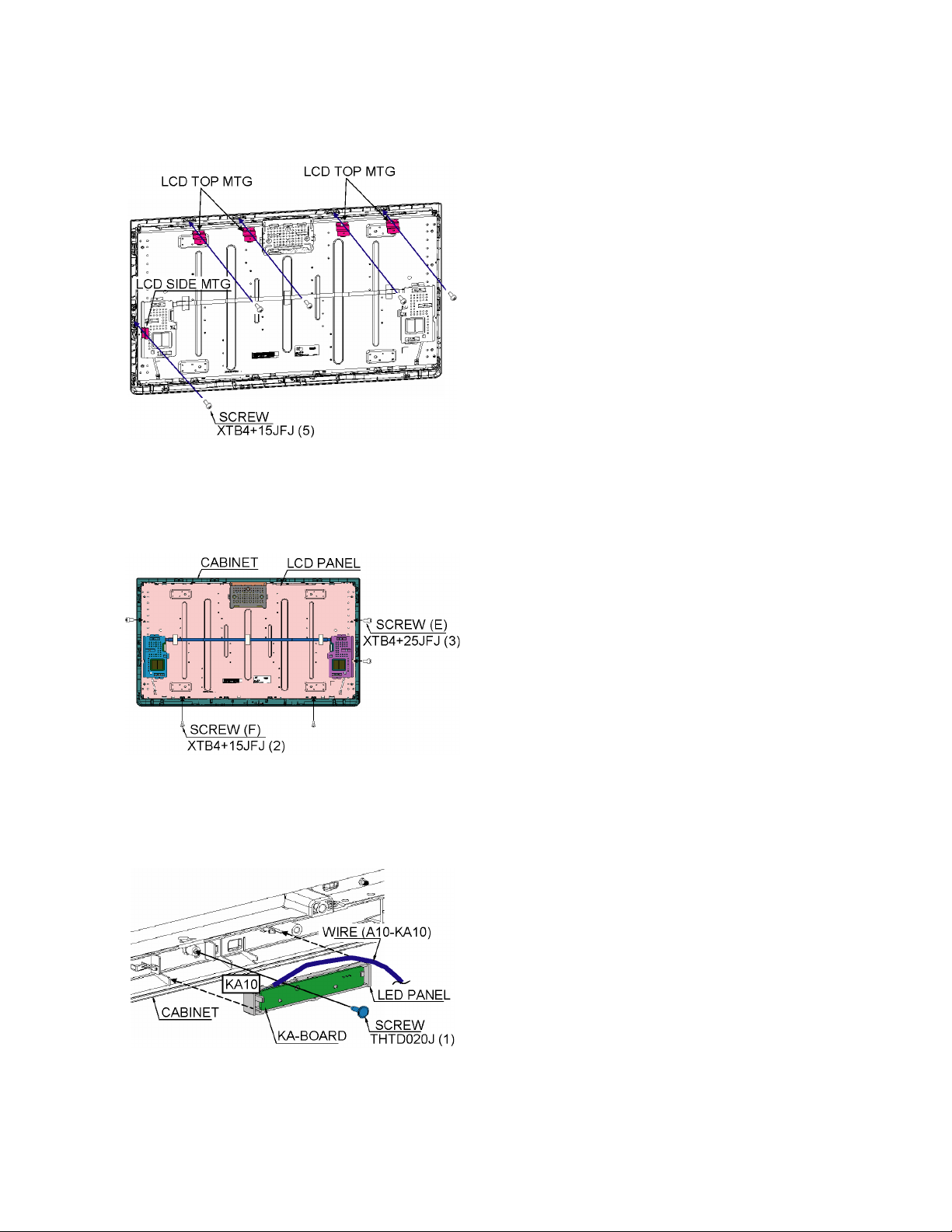
7.16. LCD Top MTG and LCD side MTG
1. Remove the 5 screws.
2. Remove the LCD Top MTG and LCD side MTG.
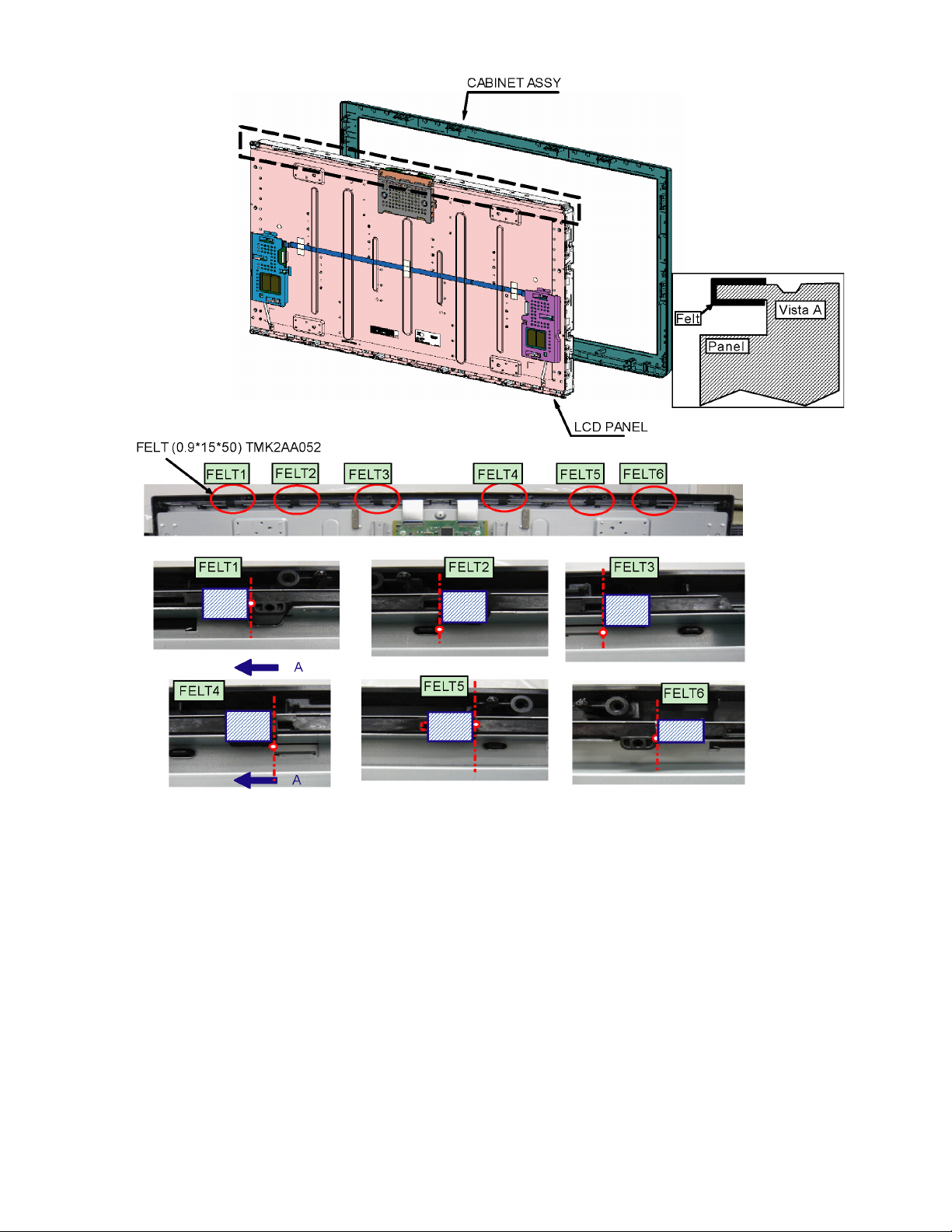
7.17. LCD Panel
1. Remove the 3 screws (E).
2. Remove the 2 screws (F).
3. Remove the LCD panel.
7.18. KA-Board
1. Remove the 1 screw.
2. Disconnect the connector (KA10).
3. Remove the KA-Board.
21
Page 22
7.19. EMI processing
22
Page 23
2324252627282930313233
Page 24
Page 25
Page 26

Page 27

Page 28

Page 29

Page 30

Page 31

Page 32

Page 33

Page 34

8 Measurements and Adjustments
8.1. VCOM Adjustment (Flicker Adjustment)
8.1.1. General information:
When replacing LCD panel, TC board (T-CON) or both, [VCOM] Adjustment have to be done.
Data for VCOM Adjustment is different depend on the LCD panel and the data is stored in TC board.
Adjustment procedures are as follows.
8.1.2. Adjustment procedures:
When replacing LCD panel, TC board or both, [VCOM] Adjustment have to be done.
1. Set to Service mode
While pressing [ VOLUME ( - ) ] button of the main unit, press [ INFO ] button of the remote control three times within 2 seconds.
2. Go into VCOM value indication
Go into main item ADJUST by pressing [1] button on remote control.
Go into sub item VCOM by pressing [3] button on remote control.
Adjustment value of VCOM is displayed.
3. Flicker Confirmation
Go to flicker adjustment screen by pressing [5] button on remote control.
Confirm if flicker can be seen.
No flicker --- Exit from Service mode.
Flicker --- Adjustment have to be done.
4. VCOM Adjustment (Flicker Adjustment)
This procedure writes into EEPROM correct data so the panel does not flicker.
Press remote control [+/ -] button to delete or minimize the flicker in flicker adjustment screen.
Press [ OK ] button. Correct data is automatically written into EEPROM (IC9206).
Caution:
The data can be written into EEPROM only 15 times. Don’t press [ OK ] button many time.
If the data can not be written, replace TC board or IC9206 to new one.
5. Exit from Service mode
Switch off the power with the [ POWER ] button on the main unit or the [ POWER ] button on the remote control.
34
Page 35

8.2. Voltage chart of A-board
VOLTAGE TEST POINT SPECIFICATION
STB3.3V TP4716 3.3 ± 0.16 V
SUB5V TP4723 5 ± 0.25 V
PANEL12V TP8307 12 ± 0.6 V
(Reception state)
8.3. Picture level adjustment (RF)
Instrument Name Remarks
1. REMOTE TRANSMITTER
2. Ex. Signal (Sprit color bar)
Adjustment or Inspection Procedure Remarks
procedure
1. Receive the Sprit color bar.
(Screen mode: ZOOM or FULL Picture mode: DYNAMIC AI: OFF AI Picture: OFF)
*BACK LIGHT +30
Inspection
1. Enter Service mode, and select MAIN_ADJ PICTURE.
Volume UP/DOWN key makes GAIN displayed under PICTURE to set.
Pushing the remote controller [OK] key for about 3 seconds, GAIN is suited
to the adjustment value automatically.
(The Sprit Color Bar Pattern)
35
Page 36

36
Page 37

(LED:1 TIME)
(LED:12 TIMES)
(LED:2 TIMES)
(LED:3 TIMES)
(LED:4 TIMES)
(LED:10 TIMES)
PFC
CIRCUIT
SUB3.3V
FILTER
(SIDE)
REMOTE RECEIVER
SUB1.2V DET
P1
SIF_OUT
LVDS DATA
STB5V
SLOT
AUDIO
SUB1.8V DET
AV SW
POWER LED(R)
R
V,Y/PB/PR
RECEIVER
RECTIFIER
A11
SUB1.2V
KA
INV_SOS
R/G/B/H/V
HDMI1
Nile-TCON
DIGITAL
CPU BUS
C.A.T.S. SENSOR
POWER LED
HDMI3
P4
SOUND SOS
REMOTE RECEIVER
P3
P
SUB3.3V
INV_SOS
DCDC
INV_ON
A03
SUB
CONVERTER
STB3.3V
INV_PWM
SUB5V
SUB3.3V
EEPROM
SUB3.3V
STB3.3V
C.A.T.S. SENSOR
SUB 3.3V SENSE
F16V
POWER SUPPLY
AC CORD
TMDS DATA
STB1.2V
SUB1.8V
K1
A10
STB3.3V
AUDIO
SD CARD DATA
SUB3.3V
KEYSCAN1
NOR
FLASH
SOS
STB5V
VIDEO_OUT
SUB_ON
RELAY
SUB_ON
PC
DDR2
SUB3.3V
POWER SW
OPERATION KEYS
LVDS-TX
F16V
STB1.2V
POWER(DVDD2.5V/AVDD12.6V/VON31V)
REMOTE IN
KA10
L
TMDS DATA
AUDIO OUT
DCDC
LIVE
P2
HDMI I/F
MAIN
DCDC
STBY5V
A
CONTROL PANEL COMP
SUB_ON
OUT
C.A.T.S. SENSOR
DCDC
SUB1.2V
F16V
ANALOG-ASIC
SD CARD
SPEAKER(L)
TUNER
SUB1.8V
INV_ON
TMDS DATA
STB5V
SUB5V
STB3.3V
INV_ON
RELAY
HDMI2
ARC
CPU BUS
I/F
ARC BUFFER SW
VIDEO/COMP. IN
IFD_OUT
ARC OFF
L/R
SPDIF
SPEAKER(R)
EEPROM
KEYSCAN3
A04
SD CARD DATA
NEUTRAL
POWER LED
INV_SOS
TU
AMP
DCDC
mini_LVDS_
RIGHT
TC06
GCLK
LVDD16V
BUCK_CONV
VGI_N/P
EEPROM
LVCC3.3V
VDD1_3.3V
LVCC3.3V
H_VDD8V
LCD PANEL
LVDD16V
TCON
PWM
LVCC3.3V
VDD1_3.3V
GMA
PNL12V
LEVEL SHIFTER
mini_
LVDS
LVDD16V
CLK
BACK LIGHT
FLASH
DCDC
ZW1.2V
LVCORE1.2V
A21
TC01
ZW1.2V
H_VDD8V
VDD
PANEL
DCDC
TC04
LVCORE1.2V
rDAC
LVDS
TC05
ZWEI2
PNL12V
mini_LVDS_
LEFT
H_VDD8V
DCDC
PNL12V
PANEL12V
TC
TCON/DOUBLE SPEED
LCD DRIVER
MAIN
CONVERTER
RELAY
(LED:1 TIME)
(LED:12 TIMES)
(LED:2 TIMES)
(LED:3 TIMES)
(LED:4 TIMES)
(LED:10 TIMES)
9 Block Diagram
9.1. Main Block Diagram
37
Page 38

9.2. Block (1/3) Diagram
HOT COLD
HOTCOLD
POWER SUPPLY
P
P1
AC CORD
1
2
Fuse
(Live)
Relay
for prevention
of inrush
ON/OFF
HOTCOLD
Start/
Stop
FILTER
+
*
*
Power
factory
correction
AC Vin
Detection
STR-6051M
(with current
limit)
->5.8V OCP
(auto restart)
PFC
over
voltage
detection
max on duty
limit
->16V/24V OCP
(auto restart)
OPERATION KEYS
POWER BUTTON
Sub converter
OVP(Latch)
Main converter T401
CONTROL PANEL COMP
/V
CH
V/
CH
+/
VOL
-/
VOL
MENU
INPUT/OK
POWER
HOT COLD
PHOTO
COUPLER
T201
*
*
PHOTO
COUPLER
PHOTO
COUPLER
*
*
*
*
PHOTO
COUPLER
PHOTO
COUPLER
P4
TO
LCD PANEL
(CN201)
FEED BACK
14
24V
+ +
+
TO
LCD PANEL
24V
(CN1)
16V/24V
over voltage
detection
P3
5.8V over
voltage
detection
1
24V
MAIN
A
FET SW
K01
1
3
P2
2
KEY1
KEY3
STB5.8V
A04
2
4
A03
15
TUNER6V
KEY1
KEY3
ON/OFF
F16V
1
F16V
+16V
+16V
+16V
RELAY
TC06
13
12
11
Q4770
8
9
4
5
3
SUB_ON
INV_ON
INV_SOS
2
4
5
6
9
SUB_ON
8
INV_ON
13
INV_SOS
12
14
INV_PWM
5
14
1213
24V
INV_ON
INV_SOS
INV_PWM
TC05
A21
1
5
46
47
49
13
24
29
40
PNL12V
24KEC_IIC1
PWM_POWER_ON
38
LVDS DATA
IC8301
PANEL12V
+12V
[R(A-D)_0+/-)]
[R(A-D)_E+/-)]LVDS DATA
3
PANEL_VCC_ON
PWM_POWER_ON
4
Page 39

9.3. Block (2/3) Diagram
(LED:2 TIMES)
(LED:3 TIMES)
(LED:1 TIME)
(LED:10 TIMES)
(LED:12 TIMES)
IC5613
3.3V
JK8502
SD CARD
IC8001
Nile TCON
(LED:10 TIMES)
SD DATA
SD CARD I/F
D2142
DIGITAL
AUDIO OUT
IEC_OUT
Q4515
ARC_OFF
JK4502
HDMI1
+5V
DDC IIC
SPDIF-OUT
TMDS DATA/CLOCK
Rx0
DDC0
HDMI_CEC
HDMI_5V_DET0
JK4501
HDMI2
DDC IIC
TMDS DATA/
CLOCK
Rx1
+5V
HDMI_CEC
DDC1
HDMI_5V_DET1
(LED:1 TIME)
JK4500
HDMI3(SIDE)
DDC IIC
TMDS DATA/
CLOCK
Rx2
DDC2
+5V
HDMI_CEC
CEC IN
HDMI_5V_DET2
CEC OUT
VIDEO/COMP. IN
PR
PB
V/Y
PB
PR
V/Y
FOR
JK2108A
PC IN
L
R
PC-B
PC-V
PC-G
PC-H
PC-R
L
R
PC-B
PC-V
PC-H
PC-R
PC-G
24KEC_IIC2
A18
FACTORY
USE
24KEC_IIC1
24KEC_IIC2
MCU_IIC
YAMON_TX/RX
SUB3.3V
IC8503
24KEC_IIC2
24KEC_IIC1
24KEC_IIC0
MCU_IIC
NAND I/F
CPU BUS
MCU_IIC
24KEC_IIC1
24KEC_IIC0
EEPROM
IC8004
MCU
EEPROM
IC8502
NOR
FLASH
STB3.3V
SPEAKER_L
SPEAKER_R
TU8302 JK2101
MAIN
A
24KEC_IIC1
F16V
1
34
A11
R(+)
R(-)
IC2106
AUDIO AMP
15V
PWM
SOS
AUDIO PWM
SOUND SOS
(LED:12 TIMES)
TUNER
SUB5V
TV_V
TV_V
ANT
24KEC_IIC0
IFD
IF_AGC
SIF
SUB5V
SUB3.3V
SIF
IFD
IF_AGC
2
1
L(-)
L(+)
IC8850
3.3V
IC5607
3.3V
LVDS3.3V
SUB3.3V_HDMI
IC5609
3.3V
SUB3.3V_A
LVDS I/F
SUB3.3V_SENSE
+3.3V
+1.8V
+1.2V
DDR I/F
MCU_XRST
KEY1
KEY3
INV ON
DAC_ENB
PANEL_VCC_ON
INVERTER_SOS
SOS[Power, Sub5, TCON, Sound]
PWM_POWER_ON
PANEL_VCC_ON
BL0PWM
AVDD_ENB
TV_SUB_ON
STB1.2V
STB3.3V
CATS_EYE
RM_IN
POWER_LED_ON
IC2110
IC5610
+1.8V
SUB1.8V
IC8002
DDR2
MCU_XRST
KEY1
KEY3
INV_ON
SOS
DAC_ENB
SUB_ON
PANEL_VCC_ON
INV_SOS
AVDD_ENB
PWM_POWER_ON
PANEL_VCC_ON
INV_PWM
AI_SENSOR
REMOTE
R_LED_ON
BUFFER
2
SUB5V
IC5608
+5V
IC5605
SUB3.3V
3.3V
SUB3.3V
F16V
IC4700
D5629
Q5612
Q5613
ON/OFF
F16V DET
3
IC5606
SUB1.2V
+1.2V
STB5V
MCU_RST
SOS
ANALOG-ASIC
SUB1.8V DET
(LED:2 TIMES)
SUB1.2V DET
(LED:3 TIMES)
STB5V
STB_RESET
PANEL SOS
STB1.2V
STB3.3V
R_LED_LED
AI_SENSOR
REMOTE
POWER LED/REMOTE RECEIVER/C.A.T.S. SENSOR
KA
POWER LED
D2800B
SUB3.3V
STB3.3V
R_LED_ON
REMOTE
KA
10
7
3
1
4
5
A10
1
5
7
AI_SENSOR
4
3
C.A.T.S.
SENSOR
SN2800
REMOTE
RECEIVER
RM2800
OUT
123
VCC
GND
IC5601
KEY3
MCU_XRST
4
POWER
KEY
RESET
39
Page 40

9.4. Block (3/3) Diagram
P2
14pin
A21
PWM_POW_ON
LVDS DATA
LVDS DATA
IIC1
PNL12V
PNL12V
FOR
FACTORY
USE
FOR
FACTORY
USE
TC07
TC08
PMW
TC06
TC05
TC
3
3
41
28
25
12
6
5
51
47
TCON/DOUBLE SPEED
Q9001
Q9003
LVDS_ODD
Z_RXAN1/P1-Z_RXDN1/P1
LVDS_EVEN
Z_RXAN0/P0-Z_RXDN0/P0
Z_IIC
PNL12V
PA9001
IC9004
ZW1.2V
VDD1_3.3V
SI/SO
L_IIC
+1.2V
+3.3V
P4
1
24V
4
P3
1
24V
5
24V
14
INV_SOS
12
INV_ON
13
INV_PWM
IC9006
ZWEI2
PWMA
OENB
RXDN1/P1
RXAN1/P1
RXDN0/P0
RXAN0/P0
IC9005
RESET
ZW1.2V
VDD1_3.3V
ZW3.3V
IC9205
BUCK_CONVERTER
VIN
IC9003
FLASH
SW
FB
NRST
SPI
+1.2V
X9001
+3.3V
XI
R1AM/P
R1DM/P
R4AM/P
R4DM/P
+3.3V
H_VDD8V
XO
SI/SO
PNL12V
mini_LVDS
L_IIC
IC9202
32Kbit
EEPROM
D9205
BACK LIGHT
LVDD16V
IC9207
DCDC
VIN
INVERTER
CIRCUIT
Q9202
SW
FB
CTRLP
FBP
SWB
FBB
FBN
CTRLN
IC9201
TCON
R1AM/P
R1DM/P
R4AM/P
R4DM/P
IIC
3.3V
1.2V
IC9203
LVCORE1.2V
+1.2V
LVDD16V
Q9201
VGL_
CONTROL
PANEL
LCD PANEL
X9201
XI
RLV0+/-
RLV6+/-
LLV0+/-
LLV6+/-
GCLK1-6
VDD_ODD
VDD_EVEN
Q9203
VDD_
CONTROL
VGH
(25-30V)
XO
D9202
CONTROL
LVCC3.3V
PANEL
Z_IIC
mini_LVDS_RIGHT
mini_LVDS_LEFT
LEVEL SHIFTER
IN1-6
IN9
IN8
VGH2
VGH1
VGL(-10V)
IC9204
OUT1-6
IC9206
IIC
OUT9
OUT8
VGL
VCOM
rDAC
VSD
OUT
VS
CLK1-6
VDD_ODD
VDD_EVEN
LVCC3.3V
H_VDD8V
LVDD16V
GMA3,4,6,7,
12,13,15,16
RMLV0N/P-RMLV5N/P
LVCC3.3V
H_VDD8V
LVDD16V
VCOMR
VDD_EVEN
VDD_ODD
VDD_ODD
VDD_EVEN
VCOML
LVDD16V
H_VDD8V
LVCC3.3V
LMLV0N/P-LMLV5N/P
GMA3,4,6,7,
12,13,15,16
VGI_P
VGI_N
CLK1-6
CLK1-6
VGI_N
VGI_P
TC01
TC04
59
48
40
27
25
24
22
21
20
19
16
12
11
10
9
8
3
58
53
52
51
50
49
44
42
41
40
39
37
36
34
21
13
2
TO
LCD PANEL
FOR RIGHT
TO
LCD PANEL
FOR LEFT
40
Page 41

10 Wiring Connection Diagram
10.1. Caution statement.
Caution:
Please confirm that all flexible cables are assembled correctly.
Also make sure that they are locked in the connectors.
Verify by giving the flexible cables a very slight pull.
10.2. Wiring
41
Page 42

42
Page 43

Model No. : TC-L42U30 Schematic Diagram Note
S-1
Page 44

Model No. : TC-L42U30 Replacement Parts List Note
S-2
Page 45

Model No. : TC-L42U30 A-Board (1/8)
S-3
Page 46

Model No. : TC-L42U30 A-Board (2/8)
S-4
Page 47

Model No. : TC-L42U30 A-Board (3/8)
S-5
Page 48

Model No. : TC-L42U30 A-Board (4/8)
S-6
Page 49

Model No. : TC-L42U30 A-Board (5/8)
S-7
Page 50

Model No. : TC-L42U30 A-Board (6/8)
S-8
Page 51

Model No. : TC-L42U30 A-Board (7/8)
S-9
Page 52

Model No. : TC-L42U30 A-Board (8/8) and KA-Board
S-10
Page 53

Model No. : TC-L42U30 TC-Board (1/3)
S-11
Page 54

Model No. : TC-L42U30 TC-Board (2/3)
S-12
Page 55

Model No. : TC-L42U30 TC-Board (3/3)
S-13
Page 56

Model No. : TC-L42U30 A-Board (Foil Side)
S-14
Page 57

Model No. : TC-L42U30 A-Board (Component Side)
S-15
Page 58

Model No. : TC-L42U30 KA-Board
S-16
Page 59

Model No. : TC-L42U30 TC-Board
S-17
Page 60

Model No. : TC-L42U30 Parts List
Safety
Ref.
No.
PCB N0AE3GK00002 CIRCUIT BOARD P 1 PAVCA
PCB TXN/A1MYUUS CIRCUIT BOARD A 1 (RTL)PAVCA
PCB TXNKA1MYUU CIRCUIT BOARD KA 1 (RTL)PAVCA
PCB TXNTC1MYUU CIRCUIT BOARD TC 1 (RTL)PAVCA
A03 K1KY15BA0324 15P CONNECTOR 1 PA VC A
A04 K1KA04B00273 4P CONNECTOR 1
A10 K1KA08B00270 8P CONNECTOR 1
A11 K1KA04BA0055 4P CONNECTOR 1
A18 K1KA14A00248 14P CONNECTOR 1
A21 K1KB51BA0074 CONNECTOR 1
C1100 F1G1E1030005 C 0.01UF 25V 1
C2103 ECJ1VB0J105K C 1UF, 6.3V 1
C2107 ECJ1VB0J105K C 1UF, 6.3V 1
C2108 ECJ1VB0J105K C 1UF, 6.3V 1
C2109 ECJ1VB0J105K C 1UF, 6.3V 1
C2111 F1G1E1030005 C 0.01UF 25V 1
C2197 F1G1E1030005 C 0.01UF 25V 1
C2198 ECJ1VB0J105K C 1UF, 6.3V 1
C2199 ECJ1VB0J105K C 1UF, 6.3V 1
C2200 ECJ1VB0J105K C 1UF, 6.3V 1
C2201 ECJ1VB0J105K C 1UF, 6.3V 1
C2202 ECJ1VB0J105K C 1UF, 6.3V 1
C2204 ECJ1VB0J105K C 1UF, 6.3V 1
C2207 F1H1A225A051 C 2.2UF, 10V 1
C2208 F1H1A225A051 C 2.2UF, 10V 1
C2209 F1H1A225A051 C 2.2UF, 10V 1
C2210 F1H1A225A051 C 2.2UF, 10V 1
C2211 F1H1A225A051 C 2.2UF, 10V 1
C2212 F1H1A225A051 C 2.2UF, 10V 1
C2213 ECJ1VB0J105K C 1UF, 6.3V 1
C2214 ECJ1VB0J105K C 1UF, 6.3V 1
C2224 F1G1H272A730 C 2700PF, 50V 1
C2226 F1G1A273A053 C0.027UF, 10V 1
C2232 ECJ1VB1E104K C 0.1 UF, 25V 1
C2234 ECJ1VB1E104K C 0.1 UF, 25V 1
C2236 F1G1H122A730 C 1200PF, 50V 1 PA VC A
C2240 ECJ2YB1A105K C 1UF, 6.3 V 1
C2241 ECJ2YB1A105K C 1UF, 6.3 V 1
C2242 ECJ2YB1A105K C 1UF, 6.3 V 1
C2243 ECJ2YB1A105K C 1UF, 6.3 V 1
C2244 F1J1E104A137 C 0.1UF, 25V 1
C2248 F1H1H223A219 C 0.022PF, 50V 1
C2249 F1H1H223A219 C 0.022PF, 50V 1
C2252 F1H1H223A219 C 0.022PF, 50V 1
C2253 F1H1H223A219 C 0.022PF, 50V 1
C2254 F1J1E104A137 C 0.1UF, 25V 1
C2256 F1H1H223A219 C 0.022PF, 50V 1
C2257 F1H1H223A219 C 0.022PF, 50V 1
C2258 F1H1H223A219 C 0.022PF, 50V 1
C2259 F1H1H223A219 C 0.022PF, 50V 1
C2260 F1G1H1020008 C 1000PF 50V 1
C2261 F1G1H1020008 C 1000PF 50V 1
C2262 F1G1H1020008 C 1000PF 50V 1
C2263 F1G1H1020008 C 1000PF 50V 1
C2266 F1K1E106A136 C 10UF, 25V 1
C2267 F1K1E106A136 C 10UF, 25V 1
C2268 F1K1E106A136 C 10UF, 25V 1
C2272 F1G1E1030005 C 0.01UF 25V 1
C2279 F1G1C104A077 C 0.1UF 16V 1
Part No. Part Name & Description Q'ty Remarks
S-18
Page 61

Model No. : TC-L42U30 Parts List
Safety
Ref.
No.
C2283 F1G1C104A077 C 0.1UF 16V 1
C2296 F1H1A225A051 C 2.2UF, 10V 1
C2297 F1H1A225A051 C 2.2UF, 10V 1
C2303 F1G1C104A077 C 0.1UF 16V 1
C2304 ECJ1VB0J105K C 1UF, 6.3V 1
C2307 ECJ1VB0J105K C 1UF, 6.3V 1
C2309 F1H1A225A051 C 2.2UF, 10V 1
C2310 F1H1A225A051 C 2.2UF, 10V 1
C2320 F1G1H122A730 C 1200PF, 50V 1 PA VC A
C2321 F1J1H474A757 C 0.47UF, 50V 1
C2322 F1G1H122A730 C 1200PF, 50V 1 PA VC A
C2323 F1J1E104A137 C 0.1UF, 25V 1
C2324 F1G1H122A730 C 1200PF, 50V 1 PA VC A
C2325 F1J1H474A757 C 0.47UF, 50V 1
C2326 F1J1E104A137 C 0.1UF, 25V 1
C2327 F1K1C3350002 C 33UF, Z, 50V 1
C2328 F1G1A105A047 C 1UF 10V 1
C2329 ECJ1VB0J105K C 1UF, 6.3V 1
C2332 F1K1E106A136 C 10UF, 25V 1
C2333 F1K1E106A136 C 10UF, 25V 1
C2334 F1G1H122A730 C 1200PF, 50V 1 PA VC A
C2335 F1G1H122A730 C 1200PF, 50V 1 PA VC A
C2336 F1G1H122A730 C 1200PF, 50V 1 PA VC A
C2337 F1G1H122A730 C 1200PF, 50V 1 PA VC A
C2340 F1K1E106A136 C 10UF, 25V 1
C2341 F1K1E106A136 C 10UF, 25V 1
C2700 F1G1E1030005 C 0.01UF 25V 1
C2701 F1G1E1030005 C 0.01UF 25V 1
C2702 F1G1E1030005 C 0.01UF 25V 1
C2703 F1G1E1030005 C 0.01UF 25V 1
C2801 F2G0J470A019 E 47UF 6.3V 1
C2802 F1G1C1030008 C 0.01UF 16V 1
C2805 ECJ1XB1C104K C 0.1UF, Z, 16V 1
C4250 ECJ1VB1H103K C 0.01UF, 50V 1
C4251 ECJ1VB1H103K C 0.01UF, 50V 1
C4252 F1K1E106A136 C 10UF, 25V 1
C4539 ECJ1VB0J105K C 1UF, 6.3V 1
C4540 ECJ1VB0J105K C 1UF, 6.3V 1
C4541 ECJ1VB0J105K C 1UF, 6.3V 1
C4546 ECJ1VB0J105K C 1UF, 6.3V 1
C4549 ECJ1VB0J105K C 1UF, 6.3V 1
C4704 F2H1A101A040 E 100 UF, 10V 1 PAVC A
C4705 F1G1C104A077 C 0.1UF 16V 1
C4706 ECJ1VB1A105K C 1UF, 10V 1
C4707 ECJ1VB1A105K C 1UF, 10V 1
C4718 F1G1C104A077 C 0.1UF 16V 1
C4721 F1G1C104A077 C 0.1UF 16V 1
C4772 F1G1C104A077 C 0.1UF 16V 1
C4779 F1J0J106A004 C 10 UF 6.3 V 1
C4780 ECJ1XC1H102J C 1000PF, J, 50V 1
C4781 ECJ1XC1H102J C 1000PF, J, 50V 1
C4792 ECJ1XC1H102J C 1000PF, J, 50V 1
C4793 ECJ1XC1H102J C 1000PF, J, 50V 1
C4797 F1K1E106A136 C 10UF, 25V 1
C4798 F1G1C104A077 C 0.1UF 16V 1
C5652 F1G1H1020008 C 1000PF 50V 1
C5663 F1J1A106A087 C 10UF, 10V 1
C5664 F1J1A106A087 C 10UF, 10V 1
C5667 F1G1H101A565 C 100PF 50V 1
C5689 F1K0J226A049 C 22UF, 6.3V 1 PAVCA
C5690 F1K0J226A049 C 22UF, 6.3V 1 PAVCA
C5692 F1K1E106A136 C 10UF, 25V 1
Part No. Part Name & Description Q'ty Remarks
S-19
Page 62

Model No. : TC-L42U30 Parts List
Safety
Ref.
No.
C5694 F1G1E1030005 C 0.01UF 25V 1
C5695 F1G1E1030005 C 0.01UF 25V 1
C5696 F1G1E472A059 C 4700pF 25V 1
C5700 F1H0J475A041 C 4.7UF, 16V 1
C5701 F1H0J475A041 C 4.7UF, 16V 1
C5702 ECJ1VB1A105K C 1UF, 10V 1
C5703 ECJ1VB1A105K C 1UF, 10V 1
C5704 F1K1E106A136 C 10UF, 25V 1
C5705 F1K1E106A136 C 10UF, 25V 1
C5706 F1G1E1030005 C 0.01UF 25V 1
C5707 F1G1C104A077 C 0.1UF 16V 1
C5708 F1K0J226A049 C 22UF, 6.3V 1 PAVCA
C5709 F1K0J226A049 C 22UF, 6.3V 1 PAVCA
C5711 F1K1E106A136 C 10UF, 25V 1
C5713 F1G1E1030005 C 0.01UF 25V 1
C5714 F1G1C153A081 C 0.015UF 16V 1
C5715 F1G1E472A059 C 4700pF 25V 1
C5719 F1K0J226A049 C 22UF, 6.3V 1 PAVCA
C5720 F1K0J226A049 C 22UF, 6.3V 1 PAVCA
C5722 F1K1E106A136 C 10UF, 25V 1
C5724 F1G1E1030005 C 0.01UF 25V 1
C5725 F1G1C153A081 C 0.015UF 16V 1
C5726 F1G1C153A081 C 0.015UF 16V 1
C5730 F1K1E106A136 C 10UF, 25V 1
C5731 F1K1E106A136 C 10UF, 25V 1
C5733 F2H1E470A007 E 47UF, 25V 1
C5734 F1J1E105A231 C 1 UF 25V 1
C5736 ECJ1VB0J105K C 1UF, 6.3V 1
C5737 ECJ1VB0J105K C 1UF, 6.3V 1
C5738 ECJ1VB0J105K C 1UF, 6.3V 1
C5739 ECJ1VB0J105K C 1UF, 6.3V 1
C5764 ECJ1VB1A105K C 1UF, 10V 1
C5765 ECJ1VB1A105K C 1UF, 10V 1
C5771 F1H1E333A029 C 0.033PF, 25V 1
C5776 F1J1A106A087 C 10UF, 10V 1
C5777 F1J1A106A087 C 10UF, 10V 1
C5778 F1G1H1020008 C 1000PF 50V 1
C5779 F1G1H1020008 C 1000PF 50V 1
C5780 F1G1H1020008 C 1000PF 50V 1
C8001 ECJ1VB0J105K C 1UF, 6.3V 1
C8002 ECJ1VB0J105K C 1UF, 6.3V 1
C8003 F1G1C104A077 C 0.1UF 16V 1
C8004 F1G1C104A077 C 0.1UF 16V 1
C8005 F1G1C104A077 C 0.1UF 16V 1
C8006 F1G1C104A077 C 0.1UF 16V 1
C8007 F1G1H6R0A732 C 6.0PF, 50V 1
C8008 F1G1H7R0A732 C 7PF, 50V 1
C8009 F1J1A475A087 C 4.7UF, 10V 1
C8011 F1G1C104A077 C 0.1UF 16V 1
C8012 F1G1C104A077 C 0.1UF 16V 1
C8013 F1G1C104A077 C 0.1UF 16V 1
C8014 F1G1C104A077 C 0.1UF 16V 1
C8015 F1G1C151A117 C 150UF 16V 1 PAVCA
C8016 F1G1C104A077 C 0.1UF 16V 1
C8017 F1G1C104A077 C 0.1UF 16V 1
C8018 F1G1C104A077 C 0.1UF 16V 1
C8019 F1G1C104A077 C 0.1UF 16V 1
C8020 F1G1C104A077 C 0.1UF 16V 1
C8021 F1G1C104A077 C 0.1UF 16V 1
C8022 F1G1C1030008 C 0.01UF 16V 1
C8023 F1G1H5R0A564 C 5 PF, 50V 1
C8024 F1G1E1030005 C 0.01UF 25V 1
Part No. Part Name & Description Q'ty Remarks
S-20
Page 63

Model No. : TC-L42U30 Parts List
Safety
Ref.
No.
C8025 F1G1C5R0A118 C 5.0PF 16V 1 PAVCA
C8026 F1G1E1030005 C 0.01UF 25V 1
C8027 F1G1C104A077 C 0.1UF 16V 1
C8028 F1G1C104A077 C 0.1UF 16V 1
C8029 F1G1E153A103 C 0.015UF 25V 1 PA VC A
C8030 F1J1A106A087 C 10UF, 10V 1
C8033 F1J1A106A087 C 10UF, 10V 1
C8034 F1G1C104A077 C 0.1UF 16V 1
C8035 F1J1A106A087 C 10UF, 10V 1
C8036 F1G1C104A077 C 0.1UF 16V 1
C8037 F1G1C104A077 C 0.1UF 16V 1
C8038 F1G1C104A077 C 0.1UF 16V 1
C8039 F1J1A106A087 C 10UF, 10V 1
C8040 F1G1C104A077 C 0.1UF 16V 1
C8041 F1J1A106A087 C 10UF, 10V 1
C8042 F1G1C104A077 C 0.1UF 16V 1
C8043 F1G1A105A047 C 1UF 10V 1
C8044 F1G1A105A047 C 1UF 10V 1
C8045 F1G1A105A047 C 1UF 10V 1
C8046 F1J0G2260001 C 22 UF 4 V 1
C8047 F1G1C104A077 C 0.1UF 16V 1
C8048 F1G1H1020008 C 1000PF 50V 1
C8049 ECJ1VB0J105K C 1UF, 6.3V 1
C8050 F1G1C104A077 C 0.1UF 16V 1
C8051 F1J1A106A087 C 10UF, 10V 1
C8053 F1G1C104A077 C 0.1UF 16V 1
C8054 F1G1C104A077 C 0.1UF 16V 1
C8056 F1G1C104A077 C 0.1UF 16V 1
C8058 F1J1A106A087 C 10UF, 10V 1
C8059 ECJ1VB0J105K C 1UF, 6.3V 1
C8060 F1G1C104A077 C 0.1UF 16V 1
C8061 F1G1H1020008 C 1000PF 50V 1
C8062 F1G1C104A077 C 0.1UF 16V 1
C8063 F1G1H1020008 C 1000PF 50V 1
C8064 ECJ1VB0J105K C 1UF, 6.3V 1
C8065 F1G1C104A077 C 0.1UF 16V 1
C8067 ECJ1VB0J105K C 1UF, 6.3V 1
C8068 ECJ1VB0J105K C 1UF, 6.3V 1
C8069 F1G1C104A077 C 0.1UF 16V 1
C8070 F1G1H1020008 C 1000PF 50V 1
C8071 F1G1C104A077 C 0.1UF 16V 1
C8073 F1G1C104A077 C 0.1UF 16V 1
C8074 F1G1H1020008 C 1000PF 50V 1
C8075 F1G1C104A077 C 0.1UF 16V 1
C8078 ECJ1VB0J105K C 1UF, 6.3V 1
C8079 ECJ1VB0J105K C 1UF, 6.3V 1
C8080 ECJ1VB0J105K C 1UF, 6.3V 1
C8081 ECJ1VB0J105K C 1UF, 6.3V 1
C8082 F1J1A106A087 C 10UF, 10V 1
C8097 F1J1A106A087 C 10UF, 10V 1
C8101 F1G1C104A077 C 0.1UF 16V 1
C8102 F1G1H5R0A564 C 5 PF, 50V 1
C8104 F1G1H1020008 C 1000PF 50V 1
C8105 F1G1H1020008 C 1000PF 50V 1
C8110 F1G1C104A077 C 0.1UF 16V 1
C8111 F1J1A106A087 C 10UF, 10V 1
C8112 F1G1H1020008 C 1000PF 50V 1
C8113 ECJ1VB0J105K C 1UF, 6.3V 1
C8116 F1G1C104A077 C 0.1UF 16V 1
C8120 F1G1C104A077 C 0.1UF 16V 1
C8121 F1G1H1020008 C 1000PF 50V 1
C8127 F1G1C104A077 C 0.1UF 16V 1
Part No. Part Name & Description Q'ty Remarks
S-21
Page 64

Model No. : TC-L42U30 Parts List
Safety
Ref.
No.
C8130 F1G1C104A077 C 0.1UF 16V 1
C8131 F1G1H1020008 C 1000PF 50V 1
C8132 ECJ1VB0J105K C 1UF, 6.3V 1
C8133 F1G1H1020008 C 1000PF 50V 1
C8136 F1G1C104A077 C 0.1UF 16V 1
C8139 F1G1C104A077 C 0.1UF 16V 1
C8140 F1G1H1020008 C 1000PF 50V 1
C8141 F1G1C104A077 C 0.1UF 16V 1
C8143 F1G1A105A047 C 1UF 10V 1
C8144 F1G1A105A047 C 1UF 10V 1
C8145 F1G1C104A077 C 0.1UF 16V 1
C8146 F1G1H1020008 C 1000PF 50V 1
C8147 F1G1C104A077 C 0.1UF 16V 1
C8148 F1G1H1020008 C 1000PF 50V 1
C8302 F1G1C104A077 C 0.1UF 16V 1
C8303 F1G1H1020008 C 1000PF 50V 1
C8304 ECJ1VB0J105K C 1UF, 6.3V 1
C8305 F1G1H221A541 C 220PF, 50V 1
C8306 F1G1H152A571 C 1500PF, 50V 1
C8307 F1G1H222A571 C 2200PF, 50V 1
C8308 F1G1C104A077 C 0.1UF 16V 1
C8312 F1G1H181A541 C 180PF, 50V 1
C8313 F1G1C104A077 C 0.1UF 16V 1
C8314 F1G1C104A077 C 0.1UF 16V 1
C8315 F1G1H1020008 C 1000PF 50V 1
C8318 F1G1H220A565 C 22PF, 50V 1
C8319 F1G1H220A565 C 22PF, 50V 1
C8324 EEEHB0J221UP E 220UF, 6.3V 1
C8328 F1G1C104A077 C 0.1UF 16V 1
C8331 F1G1H330A565 C 33PF, 50V 1
C8332 F1G1H330A565 C 33PF, 50V 1
C8333 F1G1H151A551 C 150PF, 50V 1
C8334 F1G1H221A541 C 220PF, 50V 1
C8335 F1G1H221A541 C 220PF, 50V 1
C8336 F1G1H390A565 C 39PF, 50V 1
C8337 F1G1H121A541 C 120PF, 50V 1
C8338 F1G1H121A541 C 120PF, 50V 1
C8339 F1G1H680A565 C 68PF, 50V 1
C8340 F1G1H1020008 C 1000PF 50V 1
C8341 F1G1H1020008 C 1000PF 50V 1
C8342 F1G1C104A077 C 0.1UF 16V 1
C8343 F1G1C104A077 C 0.1UF 16V 1
C8349 F1G1H1020008 C 1000PF 50V 1
C8350 F1G1C104A077 C 0.1UF 16V 1
C8351 F1G1H1020008 C 1000PF 50V 1
C8352 F1G1C104A077 C 0.1UF 16V 1
C8353 ECJ1VB0J105K C 1UF, 6.3V 1
C8354 ECJ1VB0J105K C 1UF, 6.3V 1
C8355 ECJ1VB0J105K C 1UF, 6.3V 1
C8356 F1K1E106A136 C 10UF, 25V 1
C8357 F1K1E106A136 C 10UF, 25V 1
C8358 F1G1H821A459 C 820 pF 50 V 1 PAVCA
C8359 ECJ1VB1E104K C 0.1 UF, 25V 1
C8360 F1K1E106A136 C 10UF, 25V 1
C8363 F1G1E103A059 C 0.01UF 25V 1
C8370 F1G1C104A077 C 0.1UF 16V 1
C8371 F1K1E106A136 C 10UF, 25V 1
C8372 F1K1E106A136 C 10UF, 25V 1
C8501 F1G1C104A077 C 0.1UF 16V 1
C8503 F1G1C104A077 C 0.1UF 16V 1
C8504 F1G1C104A077 C 0.1UF 16V 1
C8505 F1G1C104A077 C 0.1UF 16V 1
Part No. Part Name & Description Q'ty Remarks
S-22
Page 65

Model No. : TC-L42U30 Parts List
Safety
Ref.
No.
C8506 F1G1C104A077 C 0.1UF 16V 1
C8512 F1J1A106A087 C 10UF, 10V 1
C8513 F1G1C104A077 C 0.1UF 16V 1
C8514 F1G1E1030005 C 0.01UF 25V 1
C8515 F1J1A106A087 C 10UF, 10V 1
C8517 F1J1A106A087 C 10UF, 10V 1
C8520 F1G1C104A077 C 0.1UF 16V 1
C8851 ECJ1VB1A105K C 1UF, 10V 1
C8852 ECJ1VB1A105K C 1UF, 10V 1
C9001 F1H1H103A970 C 0.01 uF 50 V 1
C9002 F1K1E4750002 C 4.7UF, 25V 1
C9003 F1K1E4750002 C 4.7UF, 25V 1
C9028 F1G1H150A731 C 15PF, 50V 1
C9029 F1G1H180A731 C 18PF, 50V 1
C9033 ECJ1VB0J105K C 1UF, 6.3V 1
C9036 F1J1A106A087 C 10UF, 10V 1
C9037 F1G1C104A116 C 0.1UF 16V 1
C9038 F1G1C104A116 C 0.1UF 16V 1
C9039 F1G1C104A116 C 0.1UF 16V 1
C9040 F1G1C104A116 C 0.1UF 16V 1
C9041 F1G1C104A116 C 0.1UF 16V 1
C9042 F1J1A106A087 C 10UF, 10V 1
C9043 F1J1A106A087 C 10UF, 10V 1
C9044 ECJ1VB0J105K C 1UF, 6.3V 1
C9045 ECJ1VB0J105K C 1UF, 6.3V 1
C9046 F1G1C104A116 C 0.1UF 16V 1
C9047 F1G1C104A116 C 0.1UF 16V 1
C9048 F1G1C104A116 C 0.1UF 16V 1
C9049 F1G1C104A116 C 0.1UF 16V 1
C9050 F1G1C104A116 C 0.1UF 16V 1
C9051 F1G1C104A116 C 0.1UF 16V 1
C9052 F1J1A106A087 C 10UF, 10V 1
C9053 F1G1C104A116 C 0.1UF 16V 1
C9054 F1G1C104A116 C 0.1UF 16V 1
C9055 F1G1C104A116 C 0.1UF 16V 1
C9056 F1G1C104A116 C 0.1UF 16V 1
C9057 F1G1C104A116 C 0.1UF 16V 1
C9058 F1G1C104A116 C 0.1UF 16V 1
C9059 F1J1A106A087 C 10UF, 10V 1
C9060 ECJ1VB0J105K C 1UF, 6.3V 1
C9061 ECJ1VB0J105K C 1UF, 6.3V 1
C9062 F1G1C104A116 C 0.1UF 16V 1
C9063 F1G1C104A116 C 0.1UF 16V 1
C9064 F1G1C104A116 C 0.1UF 16V 1
C9065 F1G1C104A116 C 0.1UF 16V 1
C9066 F1G1C104A116 C 0.1UF 16V 1
C9067 F1G1C104A116 C 0.1UF 16V 1
C9068 F1J0J106A004 C 10 UF 6.3 V 1
C9069 F1G1C104A116 C 0.1UF 16V 1
C9070 F1G1C104A116 C 0.1UF 16V 1
C9071 F1G1C104A116 C 0.1UF 16V 1
C9072 F1G1C104A116 C 0.1UF 16V 1
C9073 ECJ1VB0J105K C 1UF, 6.3V 1
C9074 F1G1C104A116 C 0.1UF 16V 1
C9075 F1G1C104A116 C 0.1UF 16V 1
C9076 F1G1C104A116 C 0.1UF 16V 1
C9077 F1G1C104A116 C 0.1UF 16V 1
C9078 F1J0J106A004 C 10 UF 6.3 V 1
C9079 F1G1C104A116 C 0.1UF 16V 1
C9080 F1G1C104A116 C 0.1UF 16V 1
C9081 F1G1C104A116 C 0.1UF 16V 1
C9082 F1G1C104A116 C 0.1UF 16V 1
Part No. Part Name & Description Q'ty Remarks
S-23
Page 66

Model No. : TC-L42U30 Parts List
Safety
Ref.
No.
C9083 ECJ1VB0J105K C 1UF, 6.3V 1
C9084 F1G1C104A116 C 0.1UF 16V 1
C9085 F1G1C104A116 C 0.1UF 16V 1
C9086 F1G1C104A116 C 0.1UF 16V 1
C9087 F1G1C104A116 C 0.1UF 16V 1
C9088 F1G1C104A116 C 0.1UF 16V 1
C9089 F1G1C104A116 C 0.1UF 16V 1
C9090 F1G1C104A116 C 0.1UF 16V 1
C9091 F1G1C104A116 C 0.1UF 16V 1
C9092 F1G1C104A116 C 0.1UF 16V 1
C9093 F1G1C104A116 C 0.1UF 16V 1
C9094 F1G1C104A116 C 0.1UF 16V 1
C9095 F1G1C104A116 C 0.1UF 16V 1
C9097 F1G1C104A116 C 0.1UF 16V 1
C9098 F1G1C104A116 C 0.1UF 16V 1
C9099 F1G1C103A116 C 0.01UF 16V 1
C9100 F1G1H102A730 C 1000PF 50V 1
C9101 F1J1A475A087 C 4.7UF, 10V 1
C9102 F1H1C105A145 C 1 uF 16 V 1
C9103 F1G1H102A730 C 1000PF 50V 1
C9104 F1H1C104A143 C 0.1UF, 16V 1
C9105 F1H1C104A143 C 0.1UF, 16V 1
C9106 F1K1E106A136 C 10UF, 25V 1
C9107 F1K1E106A136 C 10UF, 25V 1
C9108 F1K1E106A136 C 10UF, 25V 1
C9109 F1K1E106A136 C 10UF, 25V 1
C9112 F1K0J226A008 C 22UF, 6.3V 1
C9113 F1K0J226A008 C 22UF, 6.3V 1
C9114 F1K0J226A008 C 22UF, 6.3V 1
C9115 F1K0J226A008 C 22UF, 6.3V 1
C9116 F1K0J226A008 C 22UF, 6.3V 1
C9117 F1K0J226A008 C 22UF, 6.3V 1
C9119 F1J1E105A231 C 1 UF 25V 1
C9125 F1G1C103A116 C 0.01UF 16V 1
C9126 F1G1C104A116 C 0.1UF 16V 1
C9127 F1G1C104A116 C 0.1UF 16V 1
C9128 F1G1C104A116 C 0.1UF 16V 1
C9129 F1G1C104A116 C 0.1UF 16V 1
C9130 F1G1C104A116 C 0.1UF 16V 1
C9131 F1G1C104A116 C 0.1UF 16V 1
C9132 F1G1C104A116 C 0.1UF 16V 1
C9133 F1G1C104A116 C 0.1UF 16V 1
C9134 F1G1C104A116 C 0.1UF 16V 1
C9135 F1G1C104A116 C 0.1UF 16V 1
C9136 F1G1C104A116 C 0.1UF 16V 1
C9137 F1G1C104A116 C 0.1UF 16V 1
C9138 F1G1C104A116 C 0.1UF 16V 1
C9139 F1G1C104A116 C 0.1UF 16V 1
C9140 F1G1C104A116 C 0.1UF 16V 1
C9141 F1G1C104A116 C 0.1UF 16V 1
C9142 F1G1C104A116 C 0.1UF 16V 1
C9143 F1G1C104A116 C 0.1UF 16V 1
C9144 F1G1C104A116 C 0.1UF 16V 1
C9145 F1G1C104A116 C 0.1UF 16V 1
C9146 F1G1C104A116 C 0.1UF 16V 1
C9147 F1G1C104A116 C 0.1UF 16V 1
C9152 F1G1C104A116 C 0.1UF 16V 1
C9153 F1G1C104A116 C 0.1UF 16V 1
C9154 F1G1C104A116 C 0.1UF 16V 1
C9201 F1G1C104A116 C 0.1UF 16V 1
C9202 F1G1C104A116 C 0.1UF 16V 1
C9203 F1G1C104A116 C 0.1UF 16V 1
Part No. Part Name & Description Q'ty Remarks
S-24
Page 67

Model No. : TC-L42U30 Parts List
Safety
Ref.
No.
C9204 F1G1C104A116 C 0.1UF 16V 1
C9205 F1G1C104A116 C 0.1UF 16V 1
C9206 F1G1C104A116 C 0.1UF 16V 1
C9207 F1G1C104A116 C 0.1UF 16V 1
C9208 F1G1C104A116 C 0.1UF 16V 1
C9209 F1G1C104A116 C 0.1UF 16V 1
C9210 F1G1C104A116 C 0.1UF 16V 1
C9211 F1G1C104A116 C 0.1UF 16V 1
C9212 F1G1C104A116 C 0.1UF 16V 1
C9213 F1G1C104A116 C 0.1UF 16V 1
C9214 F1G1C104A116 C 0.1UF 16V 1
C9215 F1G1C104A116 C 0.1UF 16V 1
C9216 F1G1C104A116 C 0.1UF 16V 1
C9217 F1G1C104A116 C 0.1UF 16V 1
C9218 F1G1C104A116 C 0.1UF 16V 1
C9219 F1G1C104A116 C 0.1UF 16V 1
C9220 F1G1C104A116 C 0.1UF 16V 1
C9221 F1G1C104A116 C 0.1UF 16V 1
C9222 F1G1C104A116 C 0.1UF 16V 1
C9223 F1G1C104A116 C 0.1UF 16V 1
C9224 F1G1C104A116 C 0.1UF 16V 1
C9225 F1G1C104A116 C 0.1UF 16V 1
C9226 F1G1C104A116 C 0.1UF 16V 1
C9227 F1G1C104A116 C 0.1UF 16V 1
C9228 F1G1C104A116 C 0.1UF 16V 1
C9229 F1G1C104A116 C 0.1UF 16V 1
C9230 F1G1C104A116 C 0.1UF 16V 1
C9231 F1G1C104A116 C 0.1UF 16V 1
C9232 F1G1C104A116 C 0.1UF 16V 1
C9233 F1G1C104A116 C 0.1UF 16V 1
C9234 F1G1H150A731 C 15PF, 50V 1
C9235 F1G1H150A731 C 15PF, 50V 1
C9236 F1G1C104A116 C 0.1UF 16V 1
C9237 F1J1A106A087 C 10UF, 10V 1
C9238 F1J1A106A087 C 10UF, 10V 1
C9239 F1G1C104A116 C 0.1UF 16V 1
C9240 F1G1C104A116 C 0.1UF 16V 1
C9241 F1K1E106A136 C 10UF, 25V 1
C9242 F1L1H105A059 C 1UF, Z, 50V 1 PAVC A
C9243 F1K1E106A136 C 10UF, 25V 1
C9247 F1H1C105A145 C 1 uF 16 V 1
C9248 F1J1E105A231 C 1 UF 25V 1
C9249 F1L1H105A059 C 1UF, Z, 50V 1 PAVC A
C9250 F1G1H220A731 C 22PF, 50V 1
C9251 F1K1E106A136 C 10UF, 25V 1
C9252 F1K1E106A136 C 10UF, 25V 1
C9254 F1K1E106A136 C 10UF, 25V 1
C9255 F1J1A106A087 C 10UF, 10V 1
C9256 F1H1H104A970 C 0.1UF, , 50V 1
C9257 F1J1A106A087 C 10UF, 10V 1
C9258 F1J1A106A087 C 10UF, 10V 1
C9259 F1J1A106A087 C 10UF, 10V 1
C9260 F1H1E104A129 C 0.1 uF 25V 1
C9261 F1J1C474A104 C 0.47UF, Z, 16V 1
C9262 F1H1H104A970 C 0.1UF, , 50V 1
C9263 F1K1E106A136 C 10UF, 25V 1
C9264 F1K1E106A136 C 10UF, 25V 1
C9265 F1K1E106A136 C 10UF, 25V 1
C9266 F1K1E106A136 C 10UF, 25V 1
C9267 F1K1E106A136 C 10UF, 25V 1
C9268 F1H1E104A129 C 0.1 uF 25V 1
C9269 F1H1H223A970 C 0.022UF, 50V 1
Part No. Part Name & Description Q'ty Remarks
S-25
Page 68

Model No. : TC-L42U30 Parts List
Safety
Ref.
No.
C9270 F1H1E104A129 C 0.1 uF 25V 1
C9271 F1G1H102A730 C 1000PF 50V 1
C9272 F1K1E106A136 C 10UF, 25V 1
C9273 F1G1H102A730 C 1000PF 50V 1
C9274 F1H1H104A970 C 0.1UF, , 50V 1
C9275 F1K1E106A136 C 10UF, 25V 1
C9276 F1H1H104A970 C 0.1UF, , 50V 1
C9277 F1H1H104A970 C 0.1UF, , 50V 1
C9278 F1H1H223A970 C 0.022UF, 50V 1
C9279 F1G1H221A731 C 220PF, 50V 1
C9280 F1G1H152A730 C 1500PF, 50V 1
C9283 F1H1H104A970 C 0.1UF, , 50V 1
C9284 F1J1E105A231 C 1 UF 25V 1
C9285 F1K1E106A136 C 10UF, 25V 1
C9286 F1K1E106A136 C 10UF, 25V 1
C9287 F1H1H104A970 C 0.1UF, , 50V 1
C9288 F1K1E106A136 C 10UF, 25V 1
C9289 F1H1H104A970 C 0.1UF, , 50V 1
C9290 F1K1E106A136 C 10UF, 25V 1
C9291 F1G1H121A731 C 120PF, 50V 1
C9292 F1K1H475A210 C 4.7UF, Z, 50V 1 PAVCA
C9293 F1K1H475A210 C 4.7UF, Z, 50V 1 PAVCA
C9297 F1G1C104A116 C 0.1UF 16V 1
C9298 F1K1E106A136 C 10UF, 25V 1
C9299 F1J1A106A043 C 10UF, 10V 1
C9300 F1H1H104A970 C 0.1UF, , 50V 1
C9301 F1H1H103A970 C 0.01 uF 50 V 1
C9302 F1H1E104A129 C 0.1 uF 25V 1
C9303 F1J1A106A043 C 10UF, 10V 1
C9304 F1K1E106A136 C 10UF, 25V 1
C9305 F1H1H104A970 C 0.1UF, , 50V 1
C9306 F1H1H103A970 C 0.01 uF 50 V 1
C9307 F1H1E104A129 C 0.1 uF 25V 1
C9308 F1G1C104A116 C 0.1UF 16V 1
C9309 F1G1C104A116 C 0.1UF 16V 1
C9310 F1G1C104A116 C 0.1UF 16V 1
C9311 F1G1C104A116 C 0.1UF 16V 1
C9312 F1G1C104A116 C 0.1UF 16V 1
C9313 F1G1C104A116 C 0.1UF 16V 1
C9314 F1G1C104A116 C 0.1UF 16V 1
C9315 F1H1H104A970 C 0.1UF, , 50V 1
C9316 F1H1H104A970 C 0.1UF, , 50V 1
C9317 F1H1H104A970 C 0.1UF, , 50V 1
C9318 F1K1E106A136 C 10UF, 25V 1
C9319 F1K1E106A136 C 10UF, 25V 1
C9325 F1H1H104A970 C 0.1UF, , 50V 1
C9900 F1J1E105A231 C 1 UF 25V 1
C9903 F1G1E1030005 C 0.01UF 25V 1
D1002 EZJZ0V120JA VARISTOR 1
D1003 EZJZ0V120JA VARISTOR 1
D1004 EZAEG2A50AX ESD SUPPRESSOR 1
D1005 EZAEG2A50AX ESD SUPPRESSOR 1
D1006 EZAEG2A50AX ESD SUPPRESSOR 1
D1007 EZAEG2A50AX ESD SUPPRESSOR 1
D1008 EZAEG2A50AX ESD SUPPRESSOR 1
D1009 EZAEG2A50AX ESD SUPPRESSOR 1
D1010 EZAEG2A50AX ESD SUPPRESSOR 1
D1011 EZAEG2A50AX ESD SUPPRESSOR 1
D1012 EZAEG2A50AX ESD SUPPRESSOR 1
D1013 EZAEG2A50AX ESD SUPPRESSOR 1
D1014 EZAEG2A50AX ESD SUPPRESSOR 1
Part No. Part Name & Description Q'ty Remarks
S-26
Page 69

Model No. : TC-L42U30 Parts List
Safety
Ref.
No.
D2142 K7AAAY000006 PHOTO LINK 1
D2800 B3AAB0000343 LED 1
D4101 EZJZ0V120JA VARISTOR 1
D4102 EZJZ0V120JA VARISTOR 1
D4504 DZ2J056M0L ZENER DIODE 1
D4505 DZ2J056M0L ZENER DIODE 1
D4509 DZ2J056M0L ZENER DIODE 1
D4703 B0JCME000076 DIODE 1
D4704 DA2J10100L DIODE 1
D5603 DA2J10100L DIODE 1
D5604 DA2J10100L DIODE 1
D5605 DA2J10100L DIODE 1
D5606 B0JCCE000008 DIODE 1
D5629 B0BC8R100004 ZENER DIODE 1
D5633 DA2J10100L DIODE 1
D5670 DA2J10100L DIODE 1
D5671 DA2J10100L DIODE 1
D5765 B0HCMM000014 DIODE 1
D8300 DA2J10100L DIODE 1
D8301 B0JCPG000030 DIODE 1
D8303 B0BC17000001 ZENER DIODE 1
D8304 B0BC17000001 ZENER DIODE 1
D9202 1SS355 DIODE 1
D9203 B0ECKM000048 DIODE 1
D9204 B0JCPE000004 DIODE 1
D9205 B0JCPE000004 DIODE 1
D9206 B0ECKM000048 DIODE 1
D9211 B0HCMM000014 DIODE 1
D9212 B0ECKM000048 DIODE 1
D9213 B0ECKM000048 DIODE 1
FL2100 J0HABB000003 LC FILTER 1
FL2101 J0HABB000003 LC FILTER 1
FL2102 J0HABB000004 LC FILTER 1
FL2103 J0HABB000004 LC FILTER 1
FL2104 J0HABB000004 LC FILTER 1
FL4201 EXC28CE201U FILTER 1
FL4202 EXC28CE201U FILTER 1
FL4203 EXC28CE201U FILTER 1
FL4804 EXC28CE201U FILTER 1
FL4805 EXC28CE201U FILTER 1
FL9001 EXC28CE900U NW_R(X4) 1
FL9002 EXC28CE900U NW_R(X4) 1
FL9003 EXC28CE900U NW_R(X4) 1
FL9004 EXC28CE900U NW_R(X4) 1
FL9005 EXC28CE900U NW_R(X4) 1
FL9006 EXC28CE900U NW_R(X4) 1
FL9007 EXC28CE900U NW_R(X4) 1
FL9008 EXC28CE900U NW_R(X4) 1
IC2106 C1AB00003525 IC 1 PAVCA
IC2110 C0JBAB000854 IC 1 PAVCA
IC4700 C1ZBZ0004246 IC 1
IC5601 C0EBF0000354 IC 1
IC5605 C0DBAGF00030 IC 1
IC5606 C0DBAYY00915 IC 1 PAVCA
IC5607 C0DBGYY00887 IC 1
IC5608 C0DBAYY00915 IC 1 PAVCA
IC5609 C0DBGYY00887 IC 1
IC5610 C0DBAYY00915 IC 1 PAVCA
IC5613 C0DBEYG00002 IC 1
IC8001 C1AB00003370 IC 1 PAVCA
Part No. Part Name & Description Q'ty Remarks
S-27
Page 70

Model No. : TC-L42U30 Parts List
Safety
Ref.
No.
IC8002 C3ABSY000068 IC 1 PAVCA
IC8004 TVRR986S IC 1 PAVCA
IC8301 C0DBAYY01058 IC 1 PAVCA
IC8502 TVRR984ACS IC 1 PAVCA
IC8503 TVRR987ABS IC 1 PAVCA
IC8850 C0DBGYY00930 IC 1 PAVCA
IC9003 TVRR999S IC 1 PAVCA
IC9004 C0DBAYY00715 IC 1
IC9005 C0EBM0000026 IC 1
IC9006 MN85061 IC 1 PAVCA
IC9201 C1AB00003252 IC 1 PAVCA
IC9202 TVRR448S IC 1 PAVCA
IC9203 C0CBCAG00031 IC 1
IC9204 C1AB00003246 IC 1 PAVCA
IC9205 C0DBAYY00730 IC 1 PAVCA
IC9206 TVRR457S IC 1 PAVCA
IC9207 C0DBAYY00731 IC 1 PAVCA
JK2101 K1U508A00001 CONNECTOR 1 PAVCA
JK2108A K1FY315A0011 CONNECTOR 1 PAVCA
JK4500 K1FY119E0025 CONNECTOR 1 PAVCA
JK4501 K1FY119D0015 CONNECTOR 1 PAVCA
JK4502 K1FY119D0015 CONNECTOR 1 PAVCA
JK8502 K1NA12E00017 SD CARD CONNECTOR 1
JS1003 D0GAR00J0005 M 0 OH M, 1/16W 1
KA10 K1KA07B00135 7P CONNECTOR 1
L2123 J0JCC0000287 CHIP INDUCTOR 1
L2126 J0JYC0000068 CHIP INDUCTOR 1
L2128 G1C330MA0416 INDUCTION COIL 1
L2129 G1C330MA0416 INDUCTION COIL 1
L2130 G1C330MA0416 INDUCTION COIL 1
L2131 G1C330MA0416 INDUCTION COIL 1
L2200 J0JBC0000116 COIL 1
L2201 J0JBC0000116 COIL 1
L2202 J0JBC0000116 COIL 1
L2300 J0JBC0000116 COIL 1
L2301 J0JBC0000116 COIL 1
L2302 J0JBC0000116 COIL 1
L2303 J0JBC0000116 COIL 1
L3101 J0ZZB0000142 FILTER 1 PAVCA
L3102 J0ZZB0000142 FILTER 1
L3103 J0ZZB0000142 FILTER 1
L4210 J0JHC0000045 CHIP INDUCTOR 1
L4500 J0JYC0000068 CHIP INDUCTOR 1
L4501 J0JYC0000068 CHIP INDUCTOR 1
L4502 J0JYC0000068 CHIP INDUCTOR 1
L4503 J0JYC0000068 CHIP INDUCTOR 1
L4504 J0JYC0000068 CHIP INDUCTOR 1
L4505 J0JYC0000068 CHIP INDUCTOR 1
L4506 J0JYC0000068 CHIP INDUCTOR 1
L4507 J0JYC0000068 CHIP INDUCTOR 1
L4508 J0JYC0000068 CHIP INDUCTOR 1
L4511 J0JYC0000068 CHIP INDUCTOR 1
L4512 J0JYC0000068 CHIP INDUCTOR 1
L4513 J0JYC0000068 CHIP INDUCTOR 1
L5609 G1C6R8MA0416 INDUCTION COIL 1
L5610 G1C100MA0416 INDUCTION COIL 1
L5611 G1C220MA0416 INDUCTION COIL 1
L5613 J0JHC0000075 CHIP INDUCTOR 1
Part No. Part Name & Description Q'ty Remarks
S-28
Page 71

Model No. : TC-L42U30 Parts List
Safety
Ref.
No.
L8000 J0JHC0000045 CHIP INDUCTOR 1
L8002 J0JHC0000045 CHIP INDUCTOR 1
L8003 J0JHC0000045 CHIP INDUCTOR 1
L8004 J0JHC0000045 CHIP INDUCTOR 1
L8005 J0JHC0000045 CHIP INDUCTOR 1
L8006 J0JHC0000045 CHIP INDUCTOR 1
L8008 J0JHC0000045 CHIP INDUCTOR 1
L8009 J0JHC0000045 CHIP INDUCTOR 1
L8010 J0JHC0000045 CHIP INDUCTOR 1
L8011 J0JHC0000045 CHIP INDUCTOR 1
L8012 J0JHC0000045 CHIP INDUCTOR 1
L8013 J0JHC0000045 CHIP INDUCTOR 1
L8014 J0JHC0000045 CHIP INDUCTOR 1
L8016 J0JHC0000045 CHIP INDUCTOR 1
L8017 J0JHC0000045 CHIP INDUCTOR 1
L8302 J0JGC0000070 FILTER 1
L8306 J0JHC0000045 CHIP INDUCTOR 1
L8307 G1CR22JA0020 INDUCTION COIL 1
L8308 G1CR22JA0020 INDUCTION COIL 1
L8309 G1C82NJA0075 INDUCTION COIL 1 PAVCA
L8310 G1CR10JA0020 INDUCTION COIL 1
L8311 G1CR10JA0020 INDUCTION COIL 1
L8312 G1C56NJ00018 INDUCTION COIL 1 PAVCA
L8313 G1C56NJ00018 INDUCTION COIL 1
L8314 G1CR18JA0020 INDUCTION COIL 1
L8315 J0JCC0000269 CHIP INDUCTOR 1
L8317 G1C3R3MA0425 INDUCTION COIL 1
L8500 J0JHC0000045 CHIP INDUCTOR 1
L8501 J0JHC0000045 CHIP INDUCTOR 1
L9001 G1C100MA0072 INDUCTION COIL 1
L9003 J0JHC0000045 CHIP INDUCTOR 1
L9004 J0JHC0000046 CHIP INDUCTOR 1
L9005 J0JHC0000045 CHIP INDUCTOR 1
L9006 J0JHC0000046 CHIP INDUCTOR 1
L9007 J0JYC0000068 CHIP INDUCTOR 1
L9008 J0JHC0000045 CHIP INDUCTOR 1
L9009 J0JHC0000045 CHIP INDUCTOR 1
L9010 J0JHC0000045 CHIP INDUCTOR 1
L9011 J0JHC0000045 CHIP INDUCTOR 1
L9012 J0JHC0000045 CHIP INDUCTOR 1
L9013 G1C3R3Z00004 INDUCTION COIL 1
L9014 G1C2R2Z00006 INDUCTION COIL 1
L9015 G1C100MA0077 INDUCTION COIL 1
L9016 J0JHC0000075 CHIP INDUCTOR 1
L9201 J0JHC0000046 CHIP INDUCTOR 1
L9202 G1C6R8MA0416 INDUCTION COIL 1
L9203 G1C220MA0234 INDUCTION COIL 1
L9204 G1C220MA0234 INDUCTION COIL 1
PA4803 D0GBR00J0004 M 0 OH M J 1/10W 1
PA9001 ERBSE5R00U FUSE 1
Q2760 B1ABCF000231 TRANSISTOR 1
Q2761 B1ABCF000231 TRANSISTOR 1
Q2800 DSC200100L TRANSISTOR 1
Q2802 DSC200100L TRANSISTOR 1
Q4500 DSC2001S0L TRANSISTOR 1
Q4501 DSC2001S0L TRANSISTOR 1
Q4502 DSC2001S0L TRANSISTOR 1
Q4513 B1ADCE000022 TRANSISTOR 1
Q4515 B1HFCEA00001 TRANSISTOR 1 PAVCA
Q4703 DSC2001S0L TRANSISTOR 1
Part No. Part Name & Description Q'ty Remarks
S-29
Page 72

Model No. : TC-L42U30 Parts List
Safety
Ref.
No.
Q4704 DSC2001S0L TRANSISTOR 1
Q4770 B1ADGJ000008 TRANSISTOR 1 PAVCA
Q4771 DSC2001S0L TRANSISTOR 1
Q5605 B1ADCE000022 TRANSISTOR 1
Q5612 B1ABCF000231 TRANSISTOR 1
Q5613 B1ABCF000231 TRANSISTOR 1
Q8002 B1ABCF000231 TRANSISTOR 1
Q8003 B1ABCF000231 TRANSISTOR 1
Q8005 B1CBGD000001 FET 1
Q8301 DSA2001S0L TRANSISTOR 1
Q8302 DSA2001S0L TRANSISTOR 1
Q8303 B1ABCF000231 TRANSISTOR 1
Q8304 B1ABCF000231 TRANSISTOR 1
Q8305 B1ADCE000022 TRANSISTOR 1
Q8306 B1ADCE000022 TRANSISTOR 1
Q8307 B1ABCF000231 TRANSISTOR 1
Q8308 DSA2001S0L TRANSISTOR 1
Q9001 B1ABCF000231 TRANSISTOR 1
Q9003 B1ABCF000231 TRANSISTOR 1
Q9007 B1ADCE000022 TRANSISTOR 1
Q9008 B1MBDDA00003 FET 1
Q9009 B1MBEDA00015 FET 1
Q9201 B1ABMD000006 TRANSISTOR 1 PAVCA
Q9202 B1DHCD000023 FET 1
Q9203 B1BDCF000021 TRANSISTOR 1 PAVCA
Q9900 DSC200100L TRANSISTOR 1
Q9901 DSA200100L TRANSISTOR 1
Q9902 DSC200100L TRANSISTOR 1
Q9904 DSC200100L TRANSISTOR 1
R1179 D1BB7151A055 M7.15KOHM,J.1/10W 1
R1180 D0GA102JA023 M1KOHM, J.1/16 W 1
R2114 D1BB75R0A055 M 75 OHM,J.1/10W 1
R2115 D1BB75R0A055 M 75 OHM,J.1/10W 1
R2116 D1BB75R0A055 M 75 OHM,J.1/10W 1
R2117 D0GA470JA023 M 47 OHM, J,1/16W 1
R2118 D0GA470JA023 M 47 OHM, J,1/16W 1
R2119 D0GA470JA023 M 47 OHM, J,1/16W 1
R2122 D0GA221JA023 M220 OHM, J.1/16 W 1
R2130 D0GA102JA023 M1KOHM, J.1/16 W 1
R2198 D0GA472JA023 M 4.7KOHM, J,1/16W 1
R2199 D0GA472JA023 M 4.7KOHM, J,1/16W 1
R2200 D1BB75R0A055 M 75 OHM,J.1/10W 1
R2218 D0GA680JA023 M 68 OHM, J,1/16W 1
R2223 D0GA680JA023 M 68 OHM, J,1/16W 1
R2258 D1BB75R0A055 M 75 OHM,J.1/10W 1
R2265 D1BB75R0A055 M 75 OHM,J.1/10W 1
R2283 D0GA223JA023 M 22K OHM J 1/16W 1
R2284 D0GA223JA023 M 22K OHM J 1/16W 1
R2285 D0GAR00J0005 M 0 OHM, 1/16W 1
R2287 D0GAR00J0005 M 0 OHM, 1/16W 1
R2288 D0GA223JA023 M 22K OHM J 1/16W 1
R2289 D0GAR00J0005 M 0 OHM, 1/16W 1
R2290 D0GA223JA023 M 22K OHM J 1/16W 1
R2298 D0GAR00J0005 M 0 OHM, 1/16W 1
R2299 D0GBR00J0004 M 0 OHM J 1/10W 1
R2300 D0GA151JA023 M 150 OHM, J,1/16W 1
R2302 D0GAR00J0005 M 0 OHM, 1/16W 1
R2303 D0GA151JA023 M 150 OHM, J,1/16W 1
R2304 J0JCC0000287 CHIP INDUCTOR 1
R2305 D0GA103JA015 M 10KOHM,J,1/16W 1
R2309 D0GA151JA023 M 150 OHM, J,1/16W 1
Part No. Part Name & Description Q'ty Remarks
S-30
Page 73

Model No. : TC-L42U30 Parts List
Safety
Ref.
No.
R2311 D0GA151JA023 M 150 OHM, J,1/16W 1
R2314 D0GA303JA023 M 30K OHM J 0.063W 1 PAVCA
R2324 D1BA1501A014 M 1.5KOHM,J.1/16 W 1
R2325 D1BA6801A014 M6.8 KOHM,J.1/16 W 1
R2330 D0GA103JA015 M 10KOHM,J,1/16W 1
R2331 D0GF3R3JA048 M 3.3 OHM, J,1/4W 1 PAVCA
R2332 D0GF3R3JA048 M 3.3 OHM, J,1/4W 1 PAVCA
R2333 D0GF3R3JA048 M 3.3 OHM, J,1/4W 1 PAVCA
R2334 D0GF3R3JA048 M 3.3 OHM, J,1/4W 1 PAVCA
R2348 D0GA303JA023 M 30K OHM J 0.063W 1 PAVCA
R2349 D1BA6801A014 M6.8 KOHM,J.1/16 W 1
R2350 D1BA6801A014 M6.8 KOHM,J.1/16 W 1
R2351 D0GA103JA015 M 10KOHM,J,1/16W 1
R2378 D0GA103JA015 M 10KOHM,J,1/16W 1
R2388 D0GA220JA023 M22 OHM, J.1/16 W 1
R2392 D1BA6801A014 M6.8 KOHM,J.1/16 W 1
R2700 D0GAR00J0005 M 0 OHM, 1/16W 1
R2704 D0GAR00J0005 M 0 OHM, 1/16W 1
R2757 D0GA182JA023 M 1.8KOHM, J,0.063W 1
R2760 D0GA101JA015 M 100 OHM, J,1/16W 1
R2761 D0GA101JA015 M 100 OHM, J,1/16W 1
R2762 D0GA101JA015 M 100 OHM, J,1/16W 1
R2763 D0GA473JA015 M 47KOHM, J,1/16W 1
R2764 D0GA473JA015 M 47KOHM, J,1/16W 1
R2765 D0GA103JA015 M 10KOHM,J,1/16W 1
R2766 D0GA473JA015 M 47KOHM, J,1/16W 1
R2767 D0GA102JA023 M1KOHM, J.1/16 W 1
R2769 D0GA103JA015 M 10KOHM,J,1/16W 1
R2770 D0GA473JA015 M 47KOHM, J,1/16W 1
R2801 D0GA473JA015 M 47KOHM, J,1/16W 1
R2802 D0GA223JA023 M 22K OHM J 1/16W 1
R2805 D1BA6040A014 M 604 OHM,J.1/16 W 1 PAVCA
R2806 D0GA470JA023 M 47 OHM, J,1/16W 1
R2807 D0GA562JA023 M 5.6KOHM, J,1/16W 1
R2808 D0GA184JA023 M 180KOHM J.1/16W 1
R2809 D0GA103JA015 M 10KOHM,J,1/16W 1
R2810 D0GA104JA023 M100KOHM, J.1/16 W 1
R2811 D0GA103JA015 M 10KOHM,J,1/16W 1
R2829 D0GAR00J0005 M 0 OHM, 1/16W 1
R4214 D0GBR00J0004 M 0 OHM J 1/10W 1
R4216 D0GA101JA015 M 100 OHM, J,1/16W 1
R4217 D0GA101JA015 M 100 OHM, J,1/16W 1
R4218 D0GA101JA015 M 100 OHM, J,1/16W 1
R4219 D0GA101JA015 M 100 OHM, J,1/16W 1
R4220 EXB28VR000X M 0 OHM 1/32 W 1
R4224 EXB28VR000X M 0 OHM 1/32 W 1
R4226 EXB28VR000X M 0 OHM 1/32 W 1
R4232 EXB28VR000X M 0 OHM 1/32 W 1
R4238 EXB28VR000X M 0 OHM 1/32 W 1
R4502 D0GA473JA015 M 47KOHM, J,1/16W 1
R4503 D0GA473JA015 M 47KOHM, J,1/16W 1
R4504 D0GA103JA015 M 10KOHM,J,1/16W 1
R4505 D0GA473JA015 M 47KOHM, J,1/16W 1
R4506 D0GA103JA015 M 10KOHM,J,1/16W 1
R4507 D0GA103JA015 M 10KOHM,J,1/16W 1
R4509 D0GA473JA015 M 47KOHM, J,1/16W 1
R4512 D0GA473JA015 M 47KOHM, J,1/16W 1
R4515 D0GA102JA023 M1KOHM, J.1/16 W 1
R4516 D0GA473JA015 M 47KOHM, J,1/16W 1
R4519 D0GA102JA023 M1KOHM, J.1/16 W 1
R4520 D0GA102JA023 M1KOHM, J.1/16 W 1
R4525 D0GA472JA023 M 4.7KOHM, J,1/16W 1
Part No. Part Name & Description Q'ty Remarks
S-31
Page 74

Model No. : TC-L42U30 Parts List
Safety
Ref.
No.
R4526 D0GA472JA023 M 4.7KOHM, J,1/16W 1
R4527 D0GA472JA023 M 4.7KOHM, J,1/16W 1
R4548 D0GA220JA023 M22 OHM, J.1/16 W 1
R4549 D0GA151JA023 M 150 OHM, J,1/16W 1
R4550 D0GA151JA023 M 150 OHM, J,1/16W 1
R4556 D0GA102JA023 M1KOHM, J.1/16 W 1
R4560 D0GA151JA023 M 150 OHM, J,1/16W 1
R4561 D0GA560JA023 M 56 OHM, J,1/16W 1
R4564 D0GA103JA015 M 10KOHM,J,1/16W 1
R4565 D0GA103JA015 M 10KOHM,J,1/16W 1
R4566 D0GA103JA015 M 10KOHM,J,1/16W 1
R4567 D0GA103JA015 M 10KOHM,J,1/16W 1
R4570 D0GA102JA023 M1KOHM, J.1/16 W 1
R4703 D0GDR00Z0002 M 0 OHM, 1/4W 1
R4711 D0GA472JA023 M 4.7KOHM, J,1/16W 1
R4715 D0GA222JA023 M 2.2KOHM, J,1/16W 1
R4716 D0GA222JA023 M 2.2KOHM, J,1/16W 1
R4717 D0GA222JA023 M 2.2KOHM, J,1/16W 1
R4729 D0GA222JA023 M 2.2KOHM, J,1/16W 1
R4730 D0GA222JA023 M 2.2KOHM, J,1/16W 1
R4731 D0GA222JA023 M 2.2KOHM, J,1/16W 1
R4742 D0GD150JA052 M 15 OHM,J,1/8W 1 PAVCA
R4743 D0GAR00J0005 M 0 OHM, 1/16W 1
R4762 EXB2HV220JV M 22 OHM 1/16 W 1
R4775 D0GBR00J0004 M 0 OHM J 1/10W 1
R4777 D0GA473JA015 M 47KOHM, J,1/16W 1
R4778 D0GA152JA023 M 1.5KOHM, J,0.063W 1
R4779 D0GA473JA015 M 47KOHM, J,1/16W 1
R4782 D0GA182JA023 M 1.8KOHM, J,0.063W 1
R4788 D0GA472JA023 M 4.7KOHM, J,1/16W 1
R4791 D0GDR00J0004 M 0 OHM, 1/4W 1
R4793 J0JYC0000048 CHIP INDUCTOR 1 PAVCA
R4794 D0GA102JA023 M1KOHM, J.1/16 W 1
R4795 D0GA102JA023 M1KOHM, J.1/16 W 1
R4796 D0GDR00J0004 M 0 OHM, 1/4W 1
R4803 D0GA472JA023 M 4.7KOHM, J,1/16W 1
R4809 D0GA103JA015 M 10KOHM,J,1/16W 1
R4817 D0GA103JA015 M 10KOHM,J,1/16W 1
R4820 D0GA473JA015 M 47KOHM, J,1/16W 1
R4821 D0GA103JA015 M 10KOHM,J,1/16W 1
R4822 D0GA472JA023 M 4.7KOHM, J,1/16W 1
R4823 D0GA220JA023 M22 OHM, J.1/16 W 1
R4824 D0GA220JA023 M22 OHM, J.1/16 W 1
R4830 D0GA104JA023 M100KOHM, J.1/16 W 1
R4831 D0GA104JA023 M100KOHM, J.1/16 W 1
R4861 D0GA103JA015 M 10KOHM,J,1/16W 1
R4868 D0GAR00J0005 M 0 OHM, 1/16W 1
R4872 D0GA102JA023 M1KOHM, J.1/16 W 1
R4974 D1BA1601A014 M1.60KOHM,J.1/16 W 1 PAVCA
R4975 D0GA472JA023 M 4.7KOHM, J,1/16W 1
R5609 D0GAR00J0005 M 0 OHM, 1/16W 1
R5623 D0GA103JA015 M 10KOHM,J,1/16W 1
R5624 D0GA473JA015 M 47KOHM, J,1/16W 1
R5625 D0GA683JA023 M 68KOHM, J,1/16W 1
R5626 D0GA104JA023 M100KOHM, J.1/16 W 1
R5627 D0GA103JA015 M 10KOHM,J,1/16W 1
R5629 D0GA105JA023 M 1M OHM, J,1/16W 1
R5630 D0GA101JA015 M 100 OHM, J,1/16W 1
R5631 D0GA471JA023 M 470OHM, J,1/16W 1
R5632 D0GA101JA015 M 100 OHM, J,1/16W 1
R5667 D1BB6201A087 M 6.2KOHM, J.1/10W 1
R5668 D1BB8201A087 M 8.2KOHM,J.1/10W 1
Part No. Part Name & Description Q'ty Remarks
S-32
Page 75

Model No. : TC-L42U30 Parts List
Safety
Ref.
No.
R5669 D1BA3901A014 M 3.9KOHM,J.1/16 W 1 PAVCA
R5670 D0GA223JA023 M 22K OHM J 1/16W 1
R5671 D0GA683JA023 M 68KOHM, J,1/16W 1
R5672 D0GA103JA015 M 10KOHM,J,1/16W 1
R5673 D0GA473JA015 M 47KOHM, J,1/16W 1
R5674 D0GA222JA023 M 2.2KOHM, J,1/16W 1
R5675 D0GA103JA015 M 10KOHM,J,1/16W 1
R5676 D0GA473JA015 M 47KOHM, J,1/16W 1
R5678 D1BB1202A087 M 12KOHM,J.1/10W 1
R5679 D1BB8201A087 M 8.2KOHM,J.1/10W 1
R5680 D1BA3901A014 M 3.9KOHM,J.1/16 W 1 PAVCA
R5681 D1BB4702A087 M 47KOHM,J.1/10W 1
R5682 D1BB8201A087 M 8.2KOHM,J.1/10W 1
R5683 D1BA6801A014 M6.8 KOHM,J.1/16 W 1
R5701 D1BA20010002 M 2KOHM,J.1/16 W 1
R5702 D1BA1001A014 M 1KOHM,J. 1/16 W 1
R5705 D0GDR00J0004 M 0 OHM, 1/4W 1
R5706 D0GDR00J0004 M 0 OHM, 1/4W 1
R5707 D0GB390JA041 M 39 OHM,J,1/10W 1
R5708 D0GB390JA041 M 39 OHM,J,1/10W 1
R5709 D0GB390JA041 M 39 OHM,J,1/10W 1
R5710 D0GB2R2JA065 M 2.2OHM J 1/10W 1 PAVCA
R5711 D0GB2R2JA065 M 2.2OHM J 1/10W 1 PAVCA
R5712 D0GB2R2JA065 M 2.2OHM J 1/10W 1 PAVCA
R5713 D1BB6801A087 M 6.8KOHM,J.1/10W 1
R5714 D1BB5100A087 M 510 OHM,J.1/10W 1 PAVCA
R5715 D1BB2201A087 M 2.2KOHM,J.1/10W 1
R7110 D0GA680JA023 M 68 OHM, J,1/16W 1
R7111 D0GA680JA023 M 68 OHM, J,1/16W 1
R8000 D0GA102JA023 M1KOHM, J.1/16 W 1
R8001 D0GA102JA023 M1KOHM, J.1/16 W 1
R8002 D0GA1R0JA023 M 1HM, J.1/16 W 1 PAVCA
R8003 D1BA3010A014 M 301 OHM,J.1/16 W 1 PAVCA
R8004 D1BA4020A014 M 402 OHM,J.1/16 W 1 PAVCA
R8005 D1BA1020A014 M 102 OHM,J. 1/16 W 1 PAVCA
R8006 D1BA4020A014 M 402 OHM,J.1/16 W 1 PAVCA
R8007 D1BA1020A014 M 102 OHM,J. 1/16 W 1 PAVCA
R8008 D0GA102JA023 M1KOHM, J.1/16 W 1
R8009 D0GA102JA023 M1KOHM, J.1/16 W 1
R8010 EXB28V101JX M 100 OHM 1/32 W 1
R8011 EXB28V101JX M 100 OHM 1/32 W 1
R8012 EXB28V101JX M 100 OHM 1/32 W 1
R8013 EXB28V101JX M 100 OHM 1/32 W 1
R8014 EXB28V101JX M 100 OHM 1/32 W 1
R8015 EXB28V101JX M 100 OHM 1/32 W 1
R8016 EXB28V101JX M 100 OHM 1/32 W 1
R8017 EXB28V101JX M 100 OHM 1/32 W 1
R8018 EXB28V101JX M 100 OHM 1/32 W 1
R8019 EXB28V101JX M 100 OHM 1/32 W 1
R8021 EXB28V472JX M 4.7 OHM 1/32 W 1
R8023 D0GA105JA023 M 1M OHM, J,1/16W 1
R8024 D0GA152JA023 M 1.5KOHM, J,0.063W 1
R8025 D1BB2001A055 M 2KOHM,J.1/10W 1
R8026 D1BB2001A055 M 2KOHM,J.1/10W 1
R8027 D1BB2001A055 M 2KOHM,J.1/10W 1
R8037 D0GA103JA015 M 10KOHM,J,1/16W 1
R8039 EXB28V472JX M 4.7 OHM 1/32 W 1
R8043 D0GA473JA015 M 47KOHM, J,1/16W 1
R8044 D0GA102JA023 M1KOHM, J.1/16 W 1
R8045 D0GA473JA015 M 47KOHM, J,1/16W 1
R8048 D0GA273JA023 M 27K OHM J ,1/16W 1
R8049 D0GA101JA015 M 100 OHM, J,1/16W 1
Part No. Part Name & Description Q'ty Remarks
S-33
Page 76

Model No. : TC-L42U30 Parts List
Safety
Ref.
No.
R8050 D0GA101JA015 M 100 OHM, J,1/16W 1
R8051 D0GA101JA015 M 100 OHM, J,1/16W 1
R8053 D0GA102JA023 M1KOHM, J.1/16 W 1
R8054 D0GA122JA023 M 1.2KOHM, J,1/16W 1
R8055 D0GA222JA023 M 2.2KOHM, J,1/16W 1
R8056 D0GA152JA023 M 1.5KOHM, J,0.063W 1
R8057 D0GA152JA023 M 1.5KOHM, J,0.063W 1
R8058 D0GA221JA023 M220 OHM, J.1/16 W 1
R8062 D0GA472JA023 M 4.7KOHM, J,1/16W 1
R8068 D0GA151JA023 M 150 OHM, J,1/16W 1
R8079 ERJ2RKF73R2X M73.2 OHM, F 1/16 W 1 PAVCA
R8091 D1BA80R6A014 M 80.6 OHM,J.1/16 W 1 PAVCA
R8094 D0GA472JA023 M 4.7KOHM, J,1/16W 1
R8096 D0GA472JA023 M 4.7KOHM, J,1/16W 1
R8098 D0GA472JA023 M 4.7KOHM, J,1/16W 1
R8100 D0GA223JA023 M 22K OHM J 1/16W 1
R8101 D0GA472JA023 M 4.7KOHM, J,1/16W 1
R8102 D0GA472JA023 M 4.7KOHM, J,1/16W 1
R8103 D0GA472JA023 M 4.7KOHM, J,1/16W 1
R8104 D0GA472JA023 M 4.7KOHM, J,1/16W 1
R8106 D0GAR00J0005 M 0 OHM, 1/16W 1
R8107 D0GA221JA023 M220 OHM, J.1/16 W 1
R8302 D0GA561JA023 M 560OHM, J,0.063W 1 PAVCA
R8303 D0GA102JA023 M1KOHM, J.1/16 W 1
R8305 D0GA101JA015 M 100 OHM, J,1/16W 1
R8306 D0GA222JA023 M 2.2KOHM, J,1/16W 1
R8307 D0GA101JA015 M 100 OHM, J,1/16W 1
R8308 D0GA101JA015 M 100 OHM, J,1/16W 1
R8309 D0GA750JA023 M 75 OHM, J,0.063W 1 PAVCA
R8310 D0GA474JA023 M470KOHM, J,0.063W 1 PAVCA
R8311 D0GA103JA015 M 10KOHM,J,1/16W 1
R8312 D0GA472JA023 M 4.7KOHM, J,1/16W 1
R8313 D0GA103JA015 M 10KOHM,J,1/16W 1
R8314 D0GA333JA023 M 33KOHM,J,1/16W 1
R8315 D0GA223JA023 M 22K OHM J 1/16W 1
R8317 D0GA473JA015 M 47KOHM, J,1/16W 1
R8316 D0GA473JA015 M 47KOHM, J,1/16W 1
R8318 D0GA223JA023 M 22K OHM J 1/16W 1
R8319 D0GA393JA023 M 39KOHM,J,1/16W 1 PAVCA
R8320 D0GA101JA015 M 100 OHM, J,1/16W 1
R8321 D0GA472JA023 M 4.7KOHM, J,1/16W 1
R8322 D0GA472JA023 M 4.7KOHM, J,1/16W 1
R8323 D0GA333JA023 M 33KOHM,J,1/16W 1
R8324 D0GA101JA015 M 100 OHM, J,1/16W 1
R8330 D0GA222JA023 M 2.2KOHM, J,1/16W 1
R8331 D0GA472JA023 M 4.7KOHM, J,1/16W 1
R8332 D0GA220JA023 M22 OHM, J.1/16 W 1
R8333 D0GA122JA023 M 1.2KOHM, J,1/16W 1
R8334 D0GA471JA023 M 470OHM, J,1/16W 1
R8335 D0GDR00J0004 M 0 OHM, 1/4W 1
R8336 D0GA220JA023 M22 OHM, J.1/16 W 1
R8337 D0GA102JA023 M1KOHM, J.1/16 W 1
R8339 D0GA221JA023 M220 OHM, J.1/16 W 1
R8341 D0GD821JA052 M 820 OHM,J,1/8W 1 PAVCA
R8342 D0GA102JA023 M1KOHM, J.1/16 W 1
R8389 D0GD4R7JA059 M 4.7 OHM,J,1/4W 1
R8390 D0GA101JA015 M 100 OHM, J,1/16W 1
R8391 D1BB1102A055 M 11KOHM,J.1/10W 1
R8393 D1BB8200A055 M 820 OHM,J.1/10W 1
R8394 D0GB222JA065 M 2.2KOHM,J,1/10W 1
R8395 D0GDR00J0004 M 0 OHM, 1/4W 1
R8501 D0GA680JA023 M 68 OHM, J,1/16W 1
Part No. Part Name & Description Q'ty Remarks
S-34
Page 77

Model No. : TC-L42U30 Parts List
Safety
Ref.
No.
R8512 EXB2HV680J M 68 OHM 1/16 W 1
R8513 EXB2HV680J M 68 OHM 1/16 W 1
R8514 EXB2HV680J M 68 OHM 1/16 W 1
R8515 EXB2HV680J M 68 OHM 1/16 W 1
R8516 EXB2HV680J M 68 OHM 1/16 W 1
R8528 D0GA472JA023 M 4.7KOHM, J,1/16W 1
R8530 EXB2HV330JV M 33 OHM 1/16 W 1
R8531 D0GA680JA023 M 68 OHM, J,1/16W 1
R8532 D0GA680JA023 M 68 OHM, J,1/16W 1
R8533 D0GA680JA023 M 68 OHM, J,1/16W 1
R8538 D0GA472JA023 M 4.7KOHM, J,1/16W 1
R8539 EXB2HV680J M 68 OHM 1/16 W 1
R8543 EXB2HV103JV M 10 kOHM 1/16 W 1
R8547 D0GA473JA015 M 47KOHM, J,1/16W 1
R8548 D0GA473JA015 M 47KOHM, J,1/16W 1
R8557 D0GA472JA023 M 4.7KOHM, J,1/16W 1
R8560 D0GA472JA023 M 4.7KOHM, J,1/16W 1
R8569 D0GAR00J0005 M 0 OHM, 1/16W 1
R8570 D0GAR00J0005 M 0 OHM, 1/16W 1
R8573 D0GA221JA023 M220 OHM, J.1/16 W 1
R9005 D0GA101JA015 M 100 OHM, J,1/16W 1
R9006 D0GA101JA015 M 100 OHM, J,1/16W 1
R9007 D0GA101JA015 M 100 OHM, J,1/16W 1
R9008 D0GA101JA015 M 100 OHM, J,1/16W 1
R9009 D0GA101JA015 M 100 OHM, J,1/16W 1
R9010 D0GA101JA015 M 100 OHM, J,1/16W 1
R9011 D0GA101JA015 M 100 OHM, J,1/16W 1
R9012 D0GA101JA015 M 100 OHM, J,1/16W 1
R9013 D0GA101JA015 M 100 OHM, J,1/16W 1
R9014 D0GA101JA015 M 100 OHM, J,1/16W 1
R9015 D0GA101JA015 M 100 OHM, J,1/16W 1
R9016 D0GA101JA015 M 100 OHM, J,1/16W 1
R9020 D0GBR00Z0002 M 0 OHM J 1/10W 1
R9021 ERJ2GEJ220 M 22 OHM, J,1/16 W 1
R9022 ERJ2GEJ220 M 22 OHM, J,1/16 W 1
R9023 D0GD103JA036 M 10KOHM,J,1/4W 1
R9025 D0GA392JA015 M 3.9KOHM, J,1/16W 1
R9031 D0GA473JA015 M 47KOHM, J,1/16W 1
R9036 ERJ2GEJ103 M 10KOHM, J,1/16 W 1
R9042 ERJ2GEJ103 M 10KOHM, J,1/16 W 1
R9052 ERJ2GEJ102X M 1KOHM, J.1/16 W 1
R9056 ERJ2GEJ102X M 1KOHM, J.1/16 W 1
R9066 EXB2HV103JV M 10 kOHM 1/16 W 1
R9068 D0GA334JA015 M 330KOHM, J1/16W 1
R9069 ERJ2GEJ103 M 10KOHM, J,1/16 W 1
R9070 ERJ2GEJ103 M 10KOHM, J,1/16 W 1
R9071 ERJ2GEJ103 M 10KOHM, J,1/16 W 1
R9072 ERJ2GEJ103 M 10KOHM, J,1/16 W 1
R9073 ERJ2GEJ102X M 1KOHM, J.1/16 W 1
R9074 D0GA101JA015 M 100 OHM, J,1/16W 1
R9075 ERJ2GEJ103 M 10KOHM, J,1/16 W 1
R9076 ERJ2GEJ103 M 10KOHM, J,1/16 W 1
R9078 ERJ2GEJ103 M 10KOHM, J,1/16 W 1
R9079 ERJ2GEJ103 M 10KOHM, J,1/16 W 1
R9081 ERJ2GEJ103 M 10KOHM, J,1/16 W 1
R9082 D0GA680JA015 M 68 OHM, J,1/16W 1
R9088 D0GA223JA015 M 22K OHM J 1/16W 1
R9089 EXB28V680JX M 68 OHM 1/32 W 1
R9090 ERJ2GEJ103 M 10KOHM, J,1/16 W 1
R9093 ERJ2GEJ103 M 10KOHM, J,1/16 W 1
R9094 D0GA680JA015 M 68 OHM, J,1/16W 1
R9095 ERJ2GEJ103 M 10KOHM, J,1/16 W 1
Part No. Part Name & Description Q'ty Remarks
S-35
Page 78

Model No. : TC-L42U30 Parts List
Safety
Ref.
No.
R9096 ERJ2GEJ103 M 10KOHM, J,1/16 W 1
R9097 D0GA680JA015 M 68 OHM, J,1/16W 1
R9098 D0GA680JA015 M 68 OHM, J,1/16W 1
R9099 D0GA680JA015 M 68 OHM, J,1/16W 1
R9100 ERJ2GEJ103 M 10KOHM, J,1/16 W 1
R9101 D0GA153JA015 M 15K OHM J 1/16W 1
R9102 ERJ2GEJ103 M 10KOHM, J,1/16 W 1
R9103 D1BB2492A055 M24.9KOHM,J.1/10W 1 PAVCA
R9104 D1BB2700A087 M 270 OHM,J.1/10W 1 PAVCA
R9106 D1BB4702A055 M 47KOHM,J.1/10W 1
R9107 D1BB1001A087 M 1KOHM,J.1/10W 1 PAVCA
R9108 D1BB1101A055 M 1.1 KOHM,J.1/10W 1
R9109 D1BB8200A087 M 820 OHM,J.1/10W 1
R9110 D1BB3601A055 M 3.6KOHM,J.1/10W 1
R9113 D0GA473JA015 M 47KOHM, J,1/16W 1
R9114 D0GB100JA041 M 10 OHM J 1/10W 1
R9115 D0GB100JA041 M 10 OHM J 1/10W 1
R9116 D0GAR00Z0001 M 0 OHM, 1/16W 1
R9117 D0GAR00Z0001 M 0 OHM, 1/16W 1
R9118 D1BB2702A055 M 27KOHM,J.1/10W 1
R9119 D1BB2402A055 M 24KOHM,J.1/10W 1
R9125 D0GA101JA015 M 100 OHM, J,1/16W 1
R9126 D0GA101JA015 M 100 OHM, J,1/16W 1
R9131 D0GAR00Z0001 M 0 OHM, 1/16W 1
R9152 D0GAR00Z0001 M 0 OHM, 1/16W 1
R9153 D0GAR00Z0001 M 0 OHM, 1/16W 1
R9158 ERJ2GEJ102X M 1KOHM, J.1/16 W 1
R9159 ERJ2GEJ102X M 1KOHM, J.1/16 W 1
R9160 ERJ2GEJ102X M 1KOHM, J.1/16 W 1
R9161 ERJ2GEJ102X M 1KOHM, J.1/16 W 1
R9164 D0GAR00Z0001 M 0 OHM, 1/16W 1
R9201 D0GA101JA015 M 100 OHM, J,1/16W 1
R9202 D0GA101JA015 M 100 OHM, J,1/16W 1
R9203 D0GA101JA015 M 100 OHM, J,1/16W 1
R9204 D0GA101JA015 M 100 OHM, J,1/16W 1
R9205 D0GA101JA015 M 100 OHM, J,1/16W 1
R9206 D0GA101JA015 M 100 OHM, J,1/16W 1
R9207 D0GA101JA015 M 100 OHM, J,1/16W 1
R9208 D0GA101JA015 M 100 OHM, J,1/16W 1
R9209 D0GA101JA015 M 100 OHM, J,1/16W 1
R9210 D0GA101JA015 M 100 OHM, J,1/16W 1
R9211 D0GA101JA015 M 100 OHM, J,1/16W 1
R9212 D0GA101JA015 M 100 OHM, J,1/16W 1
R9213 D0GA101JA015 M 100 OHM, J,1/16W 1
R9214 D0GA101JA015 M 100 OHM, J,1/16W 1
R9215 D0GA101JA015 M 100 OHM, J,1/16W 1
R9216 D0GA101JA015 M 100 OHM, J,1/16W 1
R9217 D0GA101JA015 M 100 OHM, J,1/16W 1
R9218 D0GA101JA015 M 100 OHM, J,1/16W 1
R9219 D0GBR00Z0002 M 0 OHM J 1/10W 1
R9221 ERJ2GEJ220 M 22 OHM, J,1/16 W 1
R9222 D0GA472JA015 M 4.7KOHM, J,1/16W 1
R9223 D0GA101JA015 M 100 OHM, J,1/16W 1
R9224 ERJ2GEJ220 M 22 OHM, J,1/16 W 1
R9225 D0GA472JA015 M 4.7KOHM, J,1/16W 1
R9226 D0GA101JA015 M 100 OHM, J,1/16W 1
R9228 D0GA101JA015 M 100 OHM, J,1/16W 1
R9229 D0GA101JA015 M 100 OHM, J,1/16W 1
R9230 D0GA101JA015 M 100 OHM, J,1/16W 1
R9232 D0GA101JA015 M 100 OHM, J,1/16W 1
R9234 D0GA680JA015 M 68 OHM, J,1/16W 1
R9235 D0GAR00Z0001 M 0 OHM, 1/16W 1
Part No. Part Name & Description Q'ty Remarks
S-36
Page 79

Model No. : TC-L42U30 Parts List
Safety
Ref.
No.
R9237 D1BA1001A014 M 1KOHM,J. 1/16 W 1
R9238 D0GAR00Z0001 M 0 OHM, 1/16W 1
R9239 D0GAR00Z0001 M 0 OHM, 1/16W 1
R9240 D1BA10R0A014 M 10 OHM,J. 1/16 W 1 PAVCA
R9242 ERJ2GEJ103 M 10KOHM, J,1/16 W 1
R9243 D1BA1004A014 M1000KOHM,J. 1/16 W 1 PAVCA
R9245 D1BA6201A014 M 6.2KOHM,J.1/16 W 1
R9246 D0GA472JA015 M 4.7KOHM, J,1/16W 1
R9247 ERJ2GEJ220 M 22 OHM, J,1/16 W 1
R9248 ERJ2GEJ220 M 22 OHM, J,1/16 W 1
R9250 D1BA1000A014 M 100 OHM,J. 1/16 W 1
R9260 D1BA20R0A014 M 20 OHM,J.1/16 W 1
R9261 D1BA20020005 M 20KOHM,J.1/16 W 1
R9262 D1BA7501A014 M 7.5 KOHM,J.1/16 W 1
R9263 D0GAR00Z0001 M 0 OHM, 1/16W 1
R9264 D1BA20R0A014 M 20 OHM,J.1/16 W 1
R9265 D1BA1000A014 M 100 OHM,J. 1/16 W 1
R9266 D1BA3001A014 M 3KOHM,J.1/16 W 1
R9267 D1BA10R0A014 M 10 OHM,J. 1/16 W 1 PAVCA
R9268 D1BA10R0A014 M 10 OHM,J. 1/16 W 1 PAVCA
R9270 D0GAR00Z0001 M 0 OHM, 1/16W 1
R9271 D1BA1003A014 M 100KOHM,J. 1/16 W 1
R9272 D1BA3602A014 M 36 KOHM,J.1/16 W 1 PAVCA
R9273 D0GAR00Z0001 M 0 OHM, 1/16W 1
R9275 D1BA3001A014 M 3KOHM,J.1/16 W 1
R9276 D0GAR00Z0001 M 0 OHM, 1/16W 1
R9278 D1BA8202A014 M 82 KOHM,J.1/16 W 1 PAVCA
R9280 D0GAR00Z0001 M 0 OHM, 1/16W 1
R9281 D0GAR00Z0001 M 0 OHM, 1/16W 1
R9283 D1BA5101A014 M 5.1KOHM,J.1/16 W 1 PAVCA
R9285 D1BA3601A014 M 3.6 KOHM,J.1/16 W 1
R9286 D1BA1302A014 M 13KOHM,J.1/16 W 1
R9287 D1BA8201A014 M 8.2 KOHM,J.1/16 W 1
R9288 D1BA1000A014 M 100 OHM,J. 1/16 W 1
R9289 D1BA2R20A014 M 2.2 OHM,J.1/16 W 1 PAVCA
R9290 D1BA2R20A014 M 2.2 OHM,J.1/16 W 1 PAVCA
R9291 D0GAR00Z0001 M 0 OHM, 1/16W 1
R9294 D1BA1003A014 M 100KOHM,J. 1/16 W 1
R9295 D0GAR00Z0001 M 0 OHM, 1/16W 1
R9296 D0GAR00Z0001 M 0 OHM, 1/16W 1
R9297 D0GAR00Z0001 M 0 OHM, 1/16W 1
R9298 D1BA20R0A014 M 20 OHM,J.1/16 W 1
R9299 D1BA20R0A014 M 20 OHM,J.1/16 W 1
R9300 D1BA1002A014 M 10KOHM,J. 1/16 W 1
R9301 D0GAR00Z0001 M 0 OHM, 1/16W 1
R9302 D0GAR00Z0001 M 0 OHM, 1/16W 1
R9303 D1BA2R20A014 M 2.2 OHM,J.1/16 W 1 PAVCA
R9306 D1BA2R20A014 M 2.2 OHM,J.1/16 W 1 PAVCA
R9307 D1BA1004A014 M1000KOHM,J. 1/16 W 1 PAVCA
R9308 D1BA1004A014 M1000KOHM,J. 1/16 W 1 PAVCA
R9309 D1BA5102A014 M 51KOHM,J.1/16 W 1
R9310 D1BA7502A014 M 75 KOHM,J.1/16 W 1 PAVCA
R9311 D1BA6802A014 M 68 KOHM,J.1/16 W 1 PAVCA
R9312 D1BA1502A014 M 15KOHM,J.1/16 W 1
R9313 D1BA5602A014 M 56KOHM,J.1/16 W 1
R9314 D1BA1003A014 M 100KOHM,J. 1/16 W 1
R9315 D1BA2R20A014 M 2.2 OHM,J.1/16 W 1 PAVCA
R9316 D1BA2R20A014 M 2.2 OHM,J.1/16 W 1 PAVCA
R9317 D1BA2R20A014 M 2.2 OHM,J.1/16 W 1 PAVCA
R9318 D1BA2R20A014 M 2.2 OHM,J.1/16 W 1 PAVCA
R9319 D1BA1602A014 M 16 OHM, J.1/16 W 1
R9320 D1BA8202A014 M 82 KOHM,J.1/16 W 1 PAVCA
Part No. Part Name & Description Q'ty Remarks
S-37
Page 80

Model No. : TC-L42U30 Parts List
Safety
Ref.
No.
R9322 ERJ8ENF9101V M 9100 OHM, 0.25W 1 PAVCA
R9324 D1BA1001A014 M 1KOHM,J. 1/16 W 1
R9327 D0GAR00Z0001 M 0 OHM, 1/16W 1
R9328 D0GAR00Z0001 M 0 OHM, 1/16W 1
R9331 D1BA2701A014 M 2.7 KOHM,J.1/16 W 1
R9332 D1BA5102A014 M 51KOHM,J.1/16 W 1
R9333 D1BA20020005 M 20KOHM,J.1/16 W 1
R9334 D1BA7501A014 M 7.5 KOHM,J.1/16 W 1
R9335 D1BA3303A014 M 330KOHM,J.1/16 W 1 PAVCA
R9336 D4CC14730006 THERMISTOR 1 PAVCA
R9337 D1BA9101A014 M 9.1 KOHM,J.1/16 W 1 PAVCA
R9338 D1BA1001A014 M 1KOHM,J. 1/16 W 1
R9339 D0GA472JA015 M 4.7KOHM, J,1/16W 1
R9349 D0GAR00Z0001 M 0 OHM, 1/16W 1
R9351 D0GAR00Z0001 M 0 OHM, 1/16W 1
R9901 D0GA103JA015 M 10KOHM,J,1/16W 1
R9902 D0GA102JA023 M1KOHM, J.1/16 W 1
R9903 D0GA473JA015 M 47KOHM, J,1/16W 1
R9904 D0GA472JA023 M 4.7KOHM, J,1/16W 1
R9907 D0GA102JA023 M1KOHM, J.1/16 W 1
R9908 D0GA102JA023 M1KOHM, J.1/16 W 1
R9909 D0GA103JA015 M 10KOHM,J,1/16W 1
R9912 D0GA103JA015 M 10KOHM,J,1/16W 1
R9915 D0GA473JA015 M 47KOHM, J,1/16W 1
R9917 D0GA682JA023 M 6.8KOHM, J,1/16W 1 PAVCA
R9919 D0GA182JA023 M 1.8KOHM, J,0.063W 1
R9922 D0GA100JA023 M 10 OHM, J,1/16W 1 PAVCA
R9923 D0GA680JA023 M 68 OHM, J,1/16W 1
RM2800 B3RAD0000168 REMOTE SENSOR 1
SN2800 B3JB00000078 IC 1
TC01 K1MN60BA0126 CONNECTOR 1 PAVCA
TC04 K1MN60BA0126 CONNECTOR 1 PAVCA
TC05 K1KB51BA0074 CONNECTOR 1
TC06 K1KA03B00242 3P CONNECTOR 1
TC07 K1KA07BA0014 7P CONNECTOR 1
TC08 K1KA09B00112 9P CONNECTOR 1
TU8302 ENG36F12KF TUNER 1 PAVCA
X8000 H0J250500094 CRYSTAL 1 PAVCA
X9001 H0J270500113 CRYSTAL 1
X9201 H2D100500004 CRYSTAL 1
ZA5400 K4ZZ01000289 TERMINAL 1 PAVCA
ZA5401 K4ZZ01000289 TERMINAL 1 PAVCA
ZA5402 K4ZZ01000289 TERMINAL 1 PAVCA
ZA5403 K4ZZ01000289 TERMINAL 1 PAVCA
ZA5406 K4ZZ01000289 TERMINAL 1 PAVCA
ZA5408 K4ZZ01000289 TERMINAL 1 PAVCA
ZA5409 K4ZZ01000289 TERMINAL 1 PAVCA
ZA5410 K4ZZ01000289 TERMINAL 1 PAVCA
ZA5412 K4ZZ01000289 TERMINAL 1 PAVCA
ZA5413 K4ZZ01000289 TERMINAL 1 PAVCA
ZA5414 K4ZZ01000289 TERMINAL 1 PAVCA
ZA5415 K4ZZ01000289 TERMINAL 1 PAVCA
ZA5417 K4ZZ01000289 TERMINAL 1 PAVCA
ZA5421 K4ZZ01000289 TERMINAL 1 PAVCA
ZA5422 K4ZZ01000289 TERMINAL 1 PAVCA
ZA5423 K4ZZ01000289 TERMINAL 1 PAVCA
Part No. Part Name & Description Q'ty Remarks
S-38
Page 81

Model No. : TC-L42U30 Exploded View
S-39
Page 82

Model No. : TC-L42U30 Parts List
Safety
Ref.
No.
1 10030-0061100 BATTERY COVER 1 PAVCA
2 K0RB00700018 CONTROL PANEL COMP 1 CIRCUIT BOARD&PANEL PAVCA
3 L0AA14B00009 SPEAKER UNIT 2 PAVCA
4 L5EDDAT00006 LCD PANEL 1 PAVCA
5 N2QAYB000 570 REMOTE CONTROL 1 PAVCA
6 TBL5ZA004 4 PEDESTAL STAND ASSY 1 PAVCA
7 TBL5ZA0046 STAND ACCESSORY ASSY 1 PAVCA
8 TKK0E9339 LED PANEL 1 PAVCA
9 TKK2AA7901 COVER (ADJ. WI ND OW) 1 PAVCA
10 TMW0E504 SP BRACKET 4 PAVCA
11 TMW2AA005 AC CODE BRACKET 1 PAVCA
12 TQB2AA0600 INSTRUCTION BOOK 1 PAVCA
13 TXFKP03ZSER SIDE AV BRACKET 1 PAVCA
14 TXFKU09ZSER REAR COVER 1 PAVCA
15 TXFKY5Z0046 CABINET ASSY 1 PAVCA
16 XYN4+F12FJK SCREW 4
Part No. Part Name & Description Q'ty Remarks
K1PY51Y00054 LVDS FFC (A21-TC05) 1 PAVCA
K2CB2YY00031 AC CORD (42) 1 PAVCA
TEWB359 GASKET(T5*W10*L60) 1
TEWB606 GASKET T25*W20*L20 5 PAVCA
TEWB755 GASKET(T5xW10xL30) 2 PAVCA
TEWF091 AL/PET TAPE 15x80 4
TEWF097 AL-Tape(W15xL40) 3
THEJ024 SCREW(TOP3/BTM4) 7
THEJ036J SCREW(T-CON2) 2
THTD020J SCREW(A5/P6/V1/CH_ F3 /SUPP_P2) 17
TKZ4GX5081 VESA METAL 4 PAVCA
TMK2AA01206 FELT(65*15*0.5) 2 PAVCA
TMK2AA052 FELT(0.9*15*50) 6 PAVCA
TMK2AG07701 SPONGE (T14XW15XL15) 1 PAVCA
TMK2AG08601 SP SPONGE(T15X30X50) 2 PAVCA
TMK2AX132 T-CON BARRIER 1 PAVCA
TMME047 CLAMPER 2
TMME268 CLAMPER 10
TMME286 SPACER 1
TSXM098 LVDS CABLE (mini 60pin) (TC01/04-LCD) 2 PAVCA
TXFMK010QJM PANEL LVDS BARRIER ASSY 1 PAVCA
TXJA11MYUU SPEAKER LEAD (A11-SP) 1 PAVCA
XSN3+6FJ SCREW 3
XTB4+15JFJ SCREW 26
XTB4+15JFJK SCREW 16
XTB4+25JFJ SCREW(PANEL3) 3
XTV3+10GFJK SCREW(REAR BRKT2) 1
XTW3+12TFJ SCREW 2
S-40
 Loading...