

Page 1
ORDER NO. PBRAS1103078CE
Service Manual
LCD TV
TC-L42S20BL
Chassis: KM09W
• Design and specications are subject to change without notice. Mass and dimensions shown are approximate.
© 2010 Panasonic do Brasil Limitada
CS Division
Technical Support
Page 2

TC-L42S20BL
CONTENTS
1 Safety Precautions ...............................................................................3
1.1. General Guidelines ...........................................................................3
1.1.1. Leakage Current Cold Check ........................................................ 3
1.1.2. Leakage Current Hot Check (See Figure1.) .................................. 3
2 Warning ................................................................................................4
2.1. Prevention of Electrostatic Discharge (ESD)
to Electrostatically Sensitive (ES) Devices .............................................. 4
2.2. About lead free solder (PbF).............................................................5
3 Service Navigation................................................................................6
3.1. Service Hint .....................................................................................6
4 Specications .......................................................................................7
5 Service Mode........................................................................................8
5.1. How to enter into Service Mode .......................................................8
5.1.1. Contents of adjustment mode........................................................8
5.1.2. How to exit .....................................................................................8
5.2. SRV-TOOL ........................................................................................9
5.2.1. How to access ...............................................................................9
5.2.2. Display of SOS History .................................................................. 9
5.2.3. POWER ON TIME/COUNT ........................................................... 9
5.2.4. Exit.................................................................................................9
5.3. Service Mode Adjustment .................................................................10
5.3.1. Self Check Mode ........................................................................... 10
5.3.2. Hotel Mode Adjustment ................................................................. 10
5.3.3. Hotel Mode ....................................................................................10
6 Troubleshooting Guide .........................................................................11
6.1. Check of the IIC bus lines.................................................................11
6.1.1. How to access ...............................................................................11
6.1.2. Exit.................................................................................................11
6.1.3. Screen display ............................................................................... 11
6.1.4. Check Point ...................................................................................11
6.2. Power LED Blinking timing chart ...................................................... 12
6.3. No Power ..........................................................................................12
7 Disassembly and Assembly Instructions .............................................. 13
7.1. AC Cord Dressing .............................................................................13
7.2. AC Cord Installation ..........................................................................14
7.3. Control Panel Assembly & Clamper Installation ............................... 15
7.4. Side AV Preparation & Installation .................................................... 16
7.5. Speaker Preparation & Installation ................................................... 17
7.6. LCD Panel Assembly Installation......................................................18
7.7. LED Panel Installation ...................................................................... 19
7.8. Felt Sticking at LVDS Wire ............................................................... 20
7.9. LCD Bracket and MTG Installation .................................................. 21
7.10. Pedestal Assembly ......................................................................... 22
8 Measurements and Adjustments .......................................................... 24
8.1. Voltage chart of A-board ................................................................... 24
8.2. Voltage chart of P-board ...................................................................24
9 Block Diagram ...................................................................................... 25
9.1. Main Block Diagram .........................................................................25
10 Wiring Connection Diagram................................................................26
11 Schematic Diagram ............................................................................ 27
11.1. Schematic Diagram Notes ..............................................................27
11.2. A Board ........................................................................................... 28
11.2.1. A Board - Sheet : 002 (1 / 3) ........................................................ 28
11.2.4. A Board - Sheet : 010 (1 / 3) ........................................................ 31
11.2.7. A Board - Sheet : 011 (1 / 3) ........................................................34
11.2.10. A Board - Sheet : 012 (1 / 3) ...................................................... 37
11.2.13. A Board - Sheet : 020 (1 / 3) ...................................................... 40
11.2.16. A Board - Sheet : 031 (1 / 3) ...................................................... 43
11.2.19. A Board - Sheet : 033 (1 / 2) ...................................................... 46
11.2.21. A Board - Sheet : 040 (1 / 5) ...................................................... 48
11.2.26. A Board - Sheet : 050 (1 / 2) ...................................................... 53
11.2.28. A Board - Sheet : 060 (1 / 2) ...................................................... 55
11.2.30. A Board - Sheet : 061 (1 / 1) ...................................................... 57
11.2.31. A Board - Sheet : 090 (1 / 3) ...................................................... 58
11.2.34. A Board - Sheet : 201 (1 / 3) ...................................................... 61
11.2.37. A Board - Sheet : 300 (1 / 4) ...................................................... 64
11.2.41. A Board - Sheet : 700 (1 / 2) ...................................................... 68
11.2.43. A Board - Sheet : 701 (1 / 2) ...................................................... 70
11.3. K Board ...........................................................................................72
11.4. P Board ........................................................................................... 74
11.5. V Board ...........................................................................................77
12 Printed Circuit Board ..........................................................................80
12.1. A-Board...........................................................................................80
12.2. A-Board...........................................................................................81
12.3. P-Board ..........................................................................................82
12.4. P-Board ..........................................................................................83
13 Exploded View and Replacement Parts List .......................................84
13.1. Exploded View and Mechanical Replacement Parts List ...............84
13.2. Electrical Replacement Parts List ...................................................84
13.2.1. Replacement Parts List Notes ..................................................... 84
13.2.2. Mechanical Parts Location ..........................................................85
13.2.3. Mechanical Replacement Parts List ............................................ 85
13.2.4. Assembled Boards.......................................................................85
13.2.5 Packing Exploded View 1 ............................................................. 86
13.2.6. Packing Exploded View 2 ............................................................ 87
13.2.7. Electrical Replacement Parts List ................................................88
2
Page 3
TC-L42S20BL
1 Safety Precautions
1.1. General Guidelines
1. When servicing, observe the original lead dress. If a short circuit is found, replace all parts which have been overheated or
damaged by the short circuit.
2. After servicing, see to it that all the protective devices such as insulation barriers, insulation papers shields are properly
installed.
3. After servicing, make the following leakage current checks to prevent the customer from being exposed to shock hazards.
4. When conducting repairs and servicing, do not attempt to modify the equipment, its parts or its materials.
5. When wiring units (with cables, flexible cables or lead wires) are supplied as repair parts and only one wire or some of the
wires have been broken or disconnected, do not attempt to repair or re-wire the units. Replace the entire wiring unit instead.
6. When conducting repairs and servicing, do not twist the Faston connectors but plug them straight in or unplug them straight
out.
1.1.1. Leakage Current Cold Check
1. Unplug the AC cord and connect a jumper between the
two prongs on the plug.
2. Measure the resistance value, with an ohmmeter,
between the jumpered AC plug and each exposed
metallic cabinet part on the equipment such as
screwheads, connectors, control shafts, etc. When the
exposed metallic part has a return path to the chassis, the
reading should be 100 Mohm and over.
When the exposed metal does not have a return path to
the chassis, the reading must be .
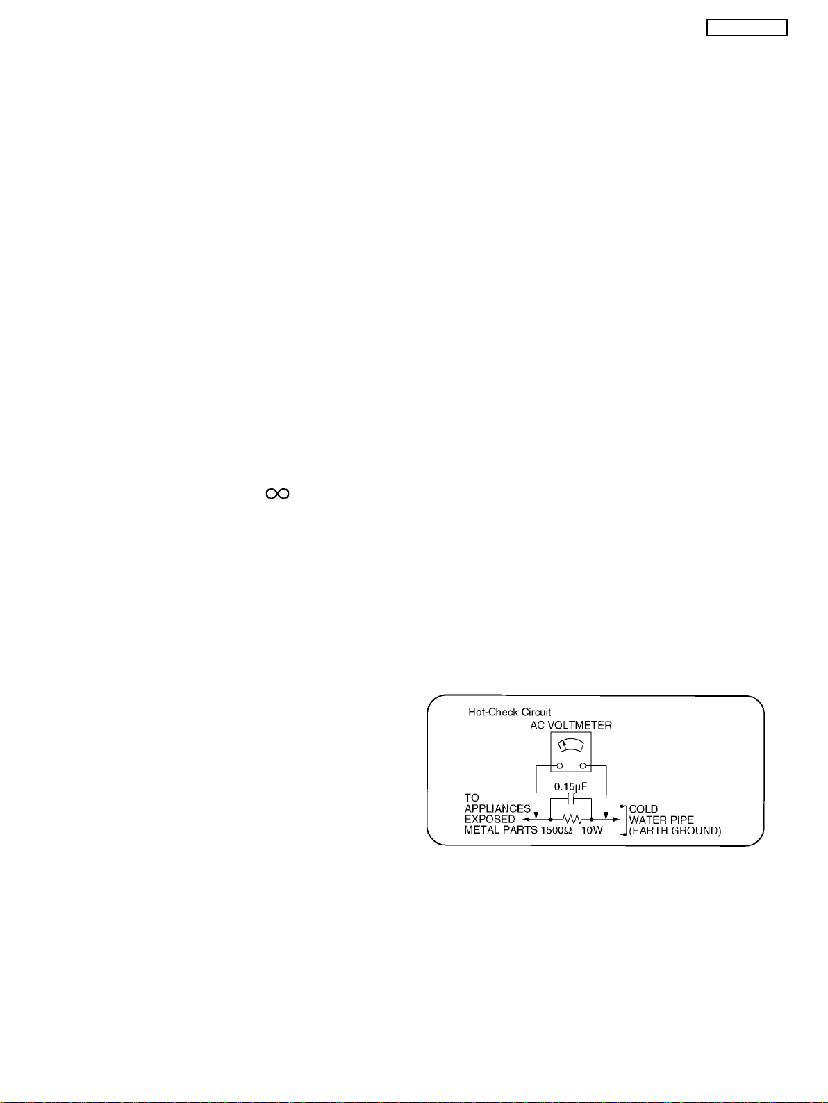
1.1.2. Leakage Current Hot Check (See
Figure 1.)
1. Plug the AC cord directly into the AC outlet. Do not use
an isolation transformer for this check.
2. Connect a 1.5kohm, 10 watts resistor, in parallel with a
0.15μF capacitors, between each exposed metallic part
on the set and a good earth ground such as a water pipe,
as shown in Figure 1.
3. Use an AC voltmeter, with 1000 ohms/volt or more
sensitivity, to measure the potential across the resistor.
4. Check each exposed metallic part, and measure the
voltage at each point.
5. Reverse the AC plug in the AC outlet and repeat each of
the above measurements.
6. The potential at any point should not exceed 0.75 volts
RMS. A leakage current tester (Simpson Model 229 or
equivalent) may be used to make the hot checks, leakage
current must not exceed 1/2 milliamp. In case a
measurement is outside of the limits specified, there is a
possibility of a shock hazard, and the equipment should
be repaired and rechecked before it is returned to the
customer.
Figure 1
3
Page 4

TC-L42S20BL
2 Warning
2.1. Prevention of Electrostatic Discharge (ESD) to Electrostatically
Sensitive (ES) Devices
Some semiconductor (solid state) devices can be damaged easily by static electricity. Such components commonly are called
Electrostatically Sensitive (ES) Devices. Examples of typical ES devices are integrated circuits and some field-effect transistors and
semiconductor [chip] components. The following techniques should be used to help reduce the incidence of component damage
caused by electrostatic discharge (ESD).
1. Immediately before handling any semiconductor component or semiconductor-equipped assembly, drain off any ESD on your
body by touching a known earth ground. Alternatively, obtain and wear a commercially available discharging ESD wrist strap,
which should be removed for potential shock reasons prior to applying power to the unit under test.
2. After removing an electrical assembly equipped with ES devices, place the assembly on a conductive surface such as
aluminum foil, to prevent electrostatic charge buildup or exposure of the assembly.
3. Use only a grounded-tip soldering iron to solder or unsolder ES devices.
4. Use only an anti-static solder removal device. Some solder removal devices not classified as [anti-static (ESD protected)] can
generate electrical charge sufficient to damage ES devices.
5. Do not use freon-propelled chemicals. These can generate electrical charges sufficient to damage ES devices.
6. Do not remove a replacement ES device from its protective package until immediately before you are ready to install it. (Most
replacement ES devices are packaged with leads electrically shorted together by conductive foam, aluminum foil or
comparable conductive material).
7. Immediately before removing the protective material from the leads of a replacement ES device, touch the protective material
to the chassis or circuit assembly into which the device will be installed.
Caution
Be sure no power is applied to the chassis or circuit, and observe all other safety precautions.
8. Minimize bodily motions when handling unpackaged replacement ES devices. (Otherwise ham less motion such as the
brushing together of your clothes fabric or the lifting of your foot from a carpeted floor can generate static electricity (ESD)
sufficient to damage an ES device).
4
Page 5
TC-L42S20BL
2.2. About lead free solder (PbF)
Note: Lead is listed as (Pb) in the periodic table of elements.
In the information below, Pb will refer to Lead solder, and PbF will refer to Lead Free Solder.
The Lead Free Solder used in our manufacturing process and discussed below is (Sn+Ag+Cu).
That is Tin (Sn), Silver (Ag) and Copper (Cu) although other types are available.
This model uses Pb Free solder in it’s manufacture due to environmental conservation issues. For service and repair work, we’d
suggest the use of Pb free solder as well, although Pb solder may be used.
PCBs manufactured using lead free solder will have the PbF within a leaf Symbol PbF stamped on the back of PCB.
Caution
• Pb free solder has a higher melting point than standard solder. Typically the melting point is 50 ~ 70 °F (30~40 °C) higher. Please
use a high temperature soldering iron and set it to 700 ± 20 °F (370 ± 10 °C).
• Pb free solder will tend to splash when heated too high (about 1100 °F or 600 °C).
If you must use Pb solder, please completely remove all of the Pb free solder on the pins or solder area before applying Pb
solder. If this is not practical, be sure to heat the Pb free solder until it melts, before applying Pb solder.
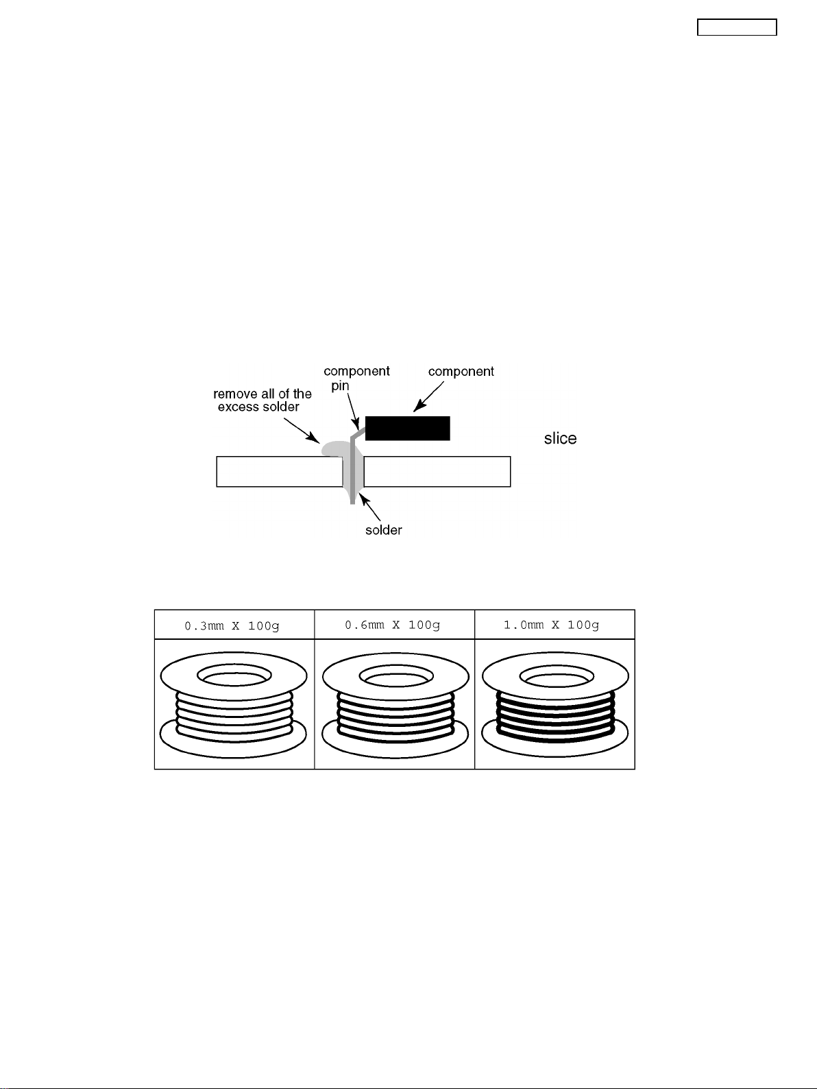
• After applying PbF solder to double layered boards, please check the component side for excess solder which may flow onto the
opposite side. (see figure below)
Suggested Pb free solder
There are several kinds of Pb free solder available for purchase. This product uses Sn+Ag+Cu (tin, silver, copper) solder.
However, Sn+Cu (tin, copper), Sn+Zn+Bi (tin, zinc, bismuth) solder can also be used.
5
Page 6
TC-L42S20BL
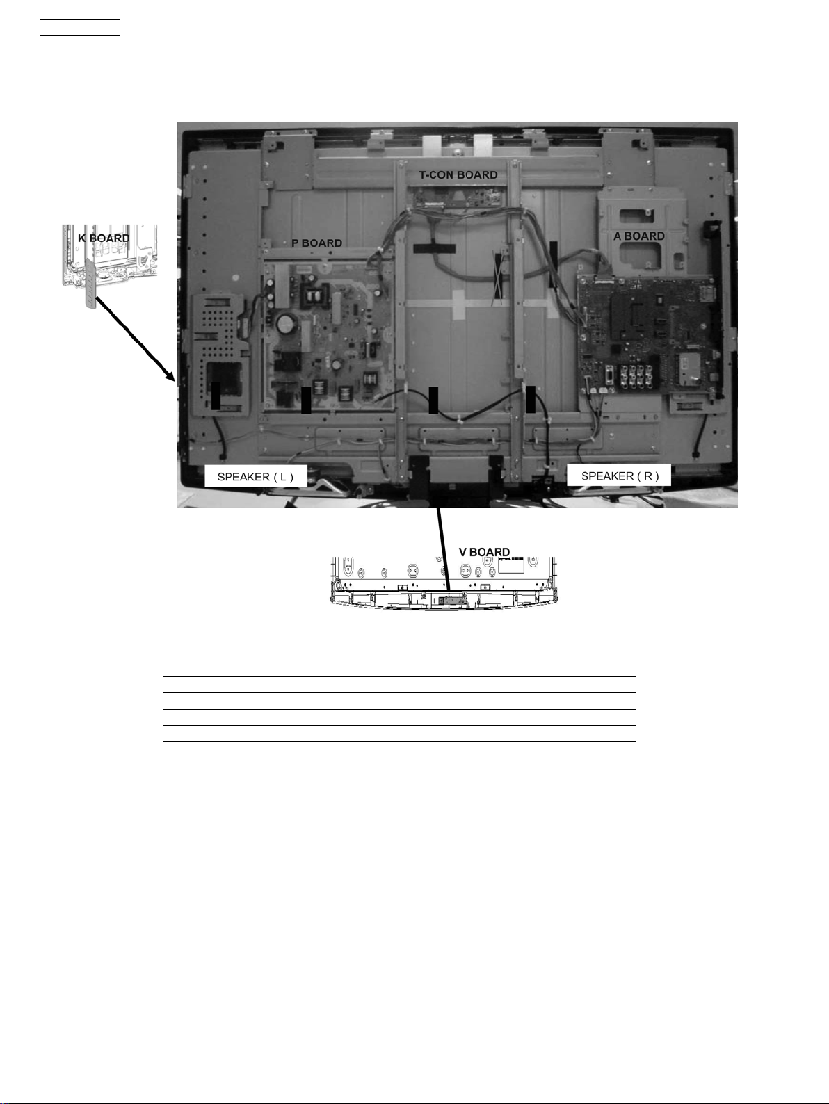
3 Service Navigation
3.1. Service Hint
Board Main Device
A BOARD AVSW, TUN, OFDM, ADV, P-AVC, GENX, EEP, TEMP
P BOARD Power Supply
V BOARD Remote, LED, Luminunce Sensor
K BOARD KEY, Power SW
TC BOARD T-CON Board
6
Page 7
4 Specications
TC-L42S20BL
TC-L42S20A / TC-L42S20P / TC-L42S20BL
Alimentación
Promedio
Condición en espera
Consumo
Aspecto
Tamaño visible de la pantalla
pantallasonido
Número de pixels
Altavoz
Salida de audio
Auriculares
Señales de computadora
Sistema de recepción/Nombre
de la banda
Canales de recepción
(TV Nor mal)
Antena - Trasera
Condiciones de operación
Entrada AUDIO L - R
AV1
Entrada AUDIO L - R
AV2
Entrada AUDIO L - R
AV3
Salida AUDIO L - R
Monitor
Terminales de conexión
Otros Entrada HDMI1/2/3
Dimensiones (L × A × P)
Peso
VIDEO
COMPONENT
VIDEO
VIDEO
VIDEO
Entrada PC
Entrada de tarjeta
Entrada USB
110-220 V ~ 50/60 Hz
193 W
0,4 W
16:9
106 cm (diagonal)
930 mm (L) × 523 mm (A)
2.073.600 (1.980 (L) × 1.080 (A)
160 mm × 42 mm × 2 pçs, 8 Ω
20 W (10 W + 10 W), 10% THD
M3 (3,5 mm) mini jack estéreo ×1
VGA, SVGA, XGA
SXGA ..... (comprimido)
Frecuencia de lectura horizontal 31 - 69 kHz
Frecuencia de lectura vertical 59 - 86 Hz
1. PAL-M
2. PAL-N
3. NTSC
BANDA VHF BANDA UHF CATV
2-13 (NTSC M EUA) 14-69 (NTSC M EUA) 1-125 (EUA CATV)
VHF / UHF
Temperatura: 0°C - 40°C
Humedad: 20% - 80% HR (sin condensación)
Tipo RCA PIN ×2 0,5 V[rms]
Tipo RCA PIN ×1 1,0 V[p-p] (75 Ω)
Y 1,0 V[p-p] (incluyendo sincronía)
PB/CB, PR/CR ±0,35 V[p-p]
Tipo RCA PIN ×2 0,5 V[rms]
Tipo RCA PIN ×1 1,0 V[p-p] (75 Ω)
Tipo RCA PIN ×2 0,5 V[rms]
Tipo RCA PIN ×1 1,0 V[p-p] (75 Ω)
Tipo RCA PIN ×2 0,5 V[rms] (alta impedáncia)
Tipo RCA PIN ×1 1,0 V[p-p] (75 Ω)
Conectores Tipo A • Este TV soporta la función “HDAVI Control 5”
HIGH-DENSITY D-SUB 15 PINES
Entrada SD CARD ×1
USB 2.0 conector Tipo A ×1, 5V DC, 500 mA máx.
1021 mm × 680 mm × 310 mm (con pedestal)
1021 mm × 637 mm × 115 mm (solamente TV)
21,0 kg (con pedestal)
18,0 kg (solamente TV)
Recepción de transmisión y reproducción en videocasete o DVD
R, G, B/0,7 V [p-p] (75 Ω)
HD, VD/TTL Nível 2,0 - 5,0 V[p-p] (alta impedáncia)
7
Page 8
TC-L42S20BL
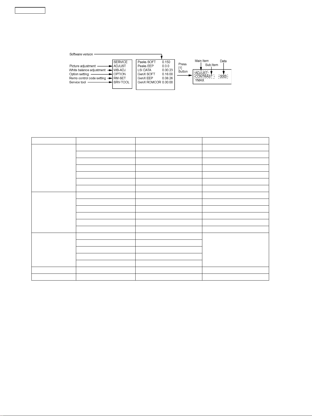
5 Service Mode
5.1. How to enter into Service Mode
While pressing [VOLUME ( - )] button of the main unit, press [INFO] button of the remote control three times within 2 seconds.
5.1.1. Contents of adjustment mode
• Value is shown as a hexadecimal number.
• Preset value differs depending on models.
• After entering the adjustment mode, take note of the value in each item before starting adjustment.
Main item Sub item Sample Data Remark
ADJUST CONTRAST 000
COLOR 4C
TINT 00
SUB-BRT 808
BACKLGT 22E
B-Y-G 34
R-Y-A 00
WB-ADJ R-GAIN F7
G-GAIN FB
B-GAIN DB
R-CENT 82
G-CENT 80
B-CENT 86
OPTION Boot ROM Factory Preset.
STBY-SET 00
EMERGENCY ON
CLK MODE 00
CLOCK 0E4
RM-SET 00 Fixed.
SRV-TOOL 00 See next.
5.1.2. How to exit
Switch off the power with the [POWER] button on the main unit or the [POWER] button on the remote control.
8
Page 9
TC-L42S20BL
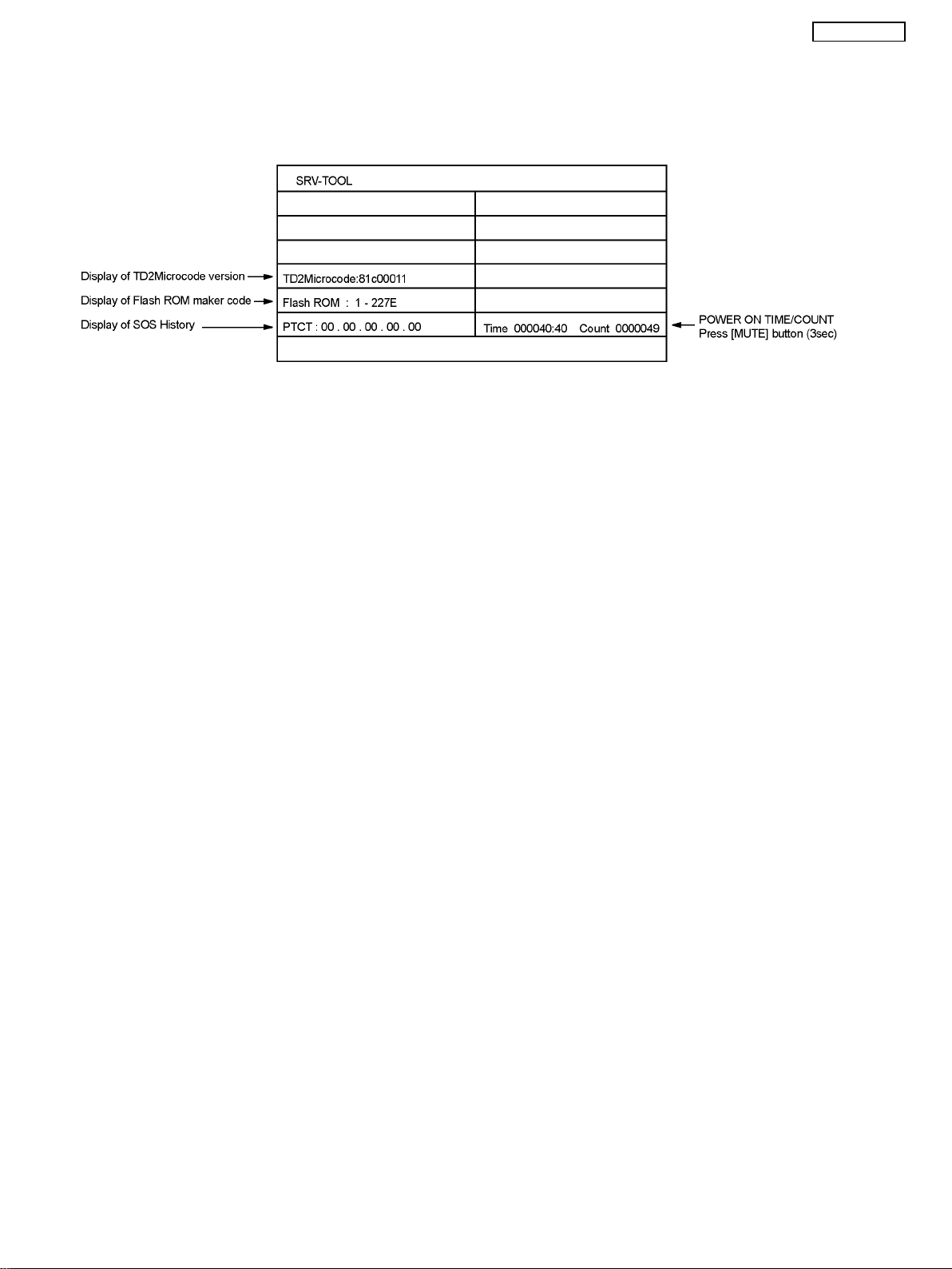
5.2. SRV-TOOL
5.2.1. How to access
1. Select [SRV-TOOL] in Service Mode.
2. Press [OK] button on the remote control.
5.2.2. Display of SOS History
SOS History (Number of LED blinking ) indication.
From left side; Last SOS, before Last, three occurrence before, 2nd occurrence after shipment, 1st occurrence after shipment.
This indication except 2nd and 1st occurrence after shipment will be cleared by [Self-check indication and forced to factory
shipment setting].
5.2.3. POWER ON TIME/COUNT
Note : To display TIME/COUNT menu, highlight position, then press MUTE for 3sec.
Time : Cumulative power on time, indicated hour : minute by decimal
Count : Number of ON times by decimal
Note : This indication will not be cleared by either of the self-checks or any other command.
5.2.4. Exit
1. Disconnect the AC cord from wall outlet.
9
Page 10
TC-L42S20BL
5.3. Service Mode Adjustment
Set timer to 30min, press the ‘RECALL’ button on the remote control and press ‘-’ vol button on the LCD panel.
• Press button R and G for adjustment.
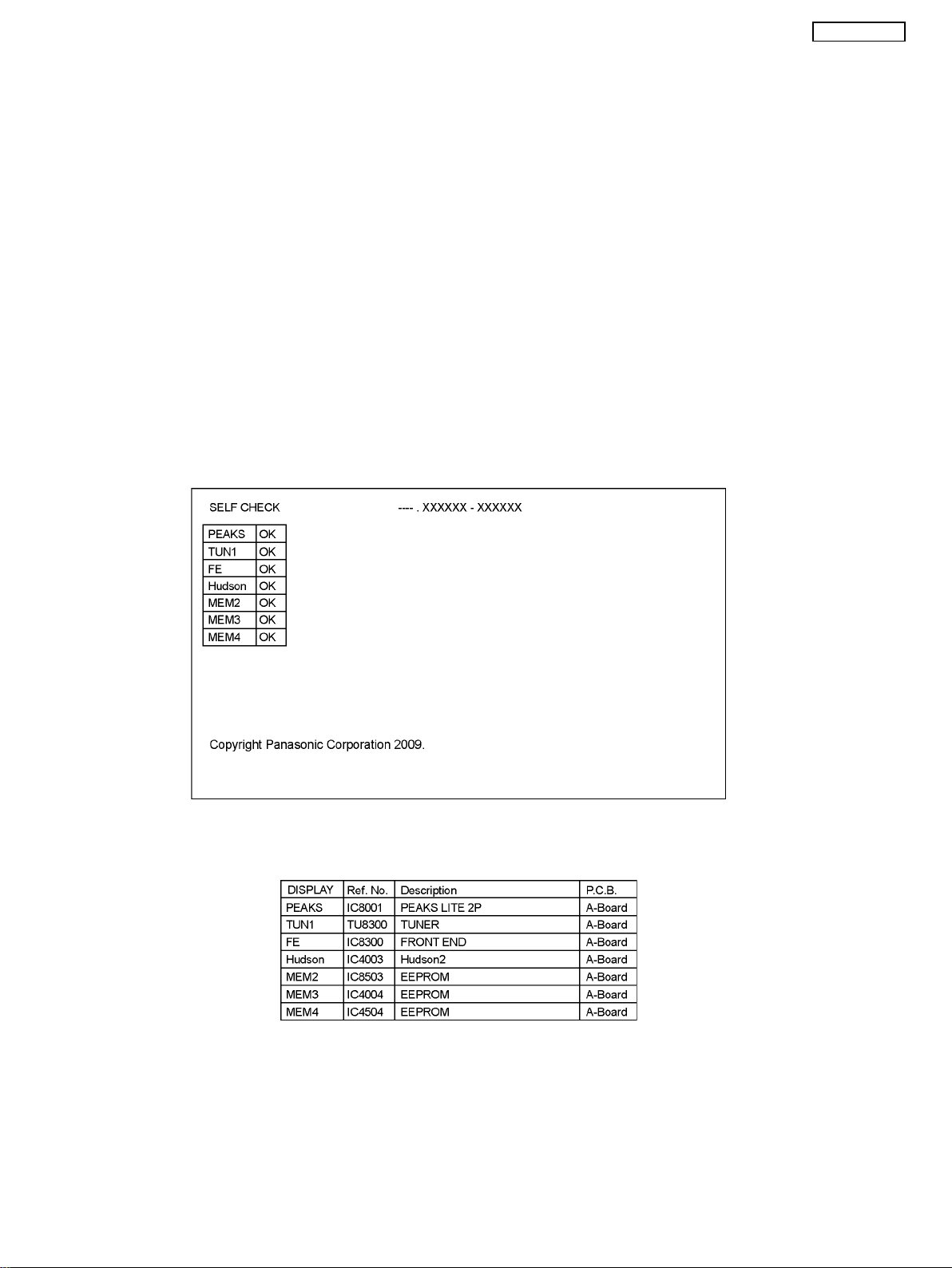
5.3.1. Self Check Mode
1. Press the ‘MENU’ button (on the remote control) and the ‘DOWN’ button on the LCD panel.
2. Press ON/OFF button on the panel to Exit.
5.3.2. Hotel Mode Adjustment
1. Press the ‘VOLUME DOWN’ button on the TV panel and simultaneously press the AV button on the remote control 3 times to
enter Hotel Mode.
2. Set Hotel mode ‘on/off’, then press ‘EXIT’ to come out.
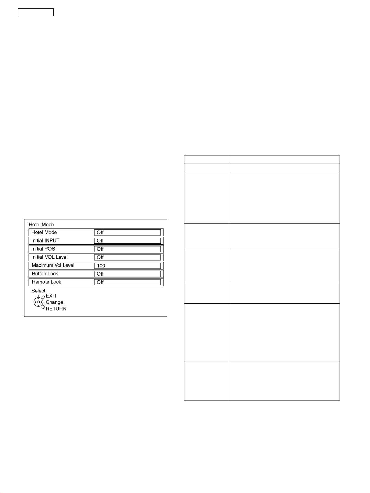
5.3.3. Hotel Mode
1. Purpose
Restrict a function for hotels.
2. Access command to the Hotel mode setup menu.
In order to display the Hotel mode setup menu, please
enter the following command (within 2 second).
[TV] : Hold Vol [Down] + [Remote] : Press AV button 3
times.
Then, the Hotel mode setup menu is displayed.
Item Function
Hotel Mode Select hotel mode ON/OFF
Initial INPUT Select input signal modes.
Set the input, when each time power is switched
on.
Selection :
OFF/Analogue TV/Digital TV/AV1/AV2/AV3/PC/
HDMI1/HDMI2/HDMI3
• Off: give priority to a last memory.
• Selectable input is depend on the model.
Initial POS Select programme number.
Initial VOL level Adjust the volume when each time power is
Maximum VOL
level
Button lock Select local key conditions.
Remote lock Select remote control key conditions.
Selection :
Off/0 to 100
• Off: give priority to a last memory.
switched on.
Selection/Range :
Off/0 to 100
• Off: give priority to a last memory.
Adjust maximum volume.
Range :
0 to 100
Selection :
Off/SETUP/MENU/All
• Off: altogether valid.
• SETUP: only F-key is invalid.
(Tuning guide (menu) can not be selected.)
• MENU: only F-key is invalid.
(only Volume/Mute can be selected.)
• ALL: altogether invalid.
Selection :
Off/SETUP/MENU
• Off: altogether valid.
• SETUP: only Setup menu is invalid.
• MENU: Picture/Sound/Setup menu are invalid.
10
Page 11
TC-L42S20BL
6 Troubleshooting Guide
Use the self-check function to test the unit.
1. Checking the IIC bus lines
2. Power LED Blinking timing
6.1. Check of the IIC bus lines
6.1.1. How to access
Self-check indication only:
Produce TV reception screen, and while pressing [VOLUME ( - )] button on the main unit, press [OK] button on the remote control
for more than 3 seconds.
Self-check indication and forced to factory shipment setting:
Produce TV reception screen, and while pressing [VOLUME ( - )] button on the main unit, press [MENU] button on the remote
control for more than 3 seconds.
6.1.2. Exit
Disconnect the AC cord from wall outlet.
6.1.3. Screen display
6.1.4. Check Point
Confirm the following parts if NG was displayed.
11
Page 12
TC-L42S20BL
6.2. Power LED Blinking timing chart
1. Subject
Information of LED Flashing timing chart.
2. Contents
When an abnormality occurs, the protection circuit will operate and reset the unit to stand by mode. During this time, the
defective block can be identified by the number of blinking times of the Power LED on the front panel of the unit as follow:
Blinking times Contents BOARD
1 Inverter_SOS P BOARD
2 FAN_SOS A BOARD
3 SOS A BOARD
4 DTV_9V P/A BOARD
5 MAIN_9V A BOARD
6 SUB_5V A BOARD
7 SUB_3.3V A BOARD
8 MAIN_3.3V A BOARD
9 SOUND_SOS A BOARD
10 HQ1L_SOS / ZWEI_SOS A BOARD
13 EMERGENCY SOS A BOARD
14 Audio PWM SOS A BOARD
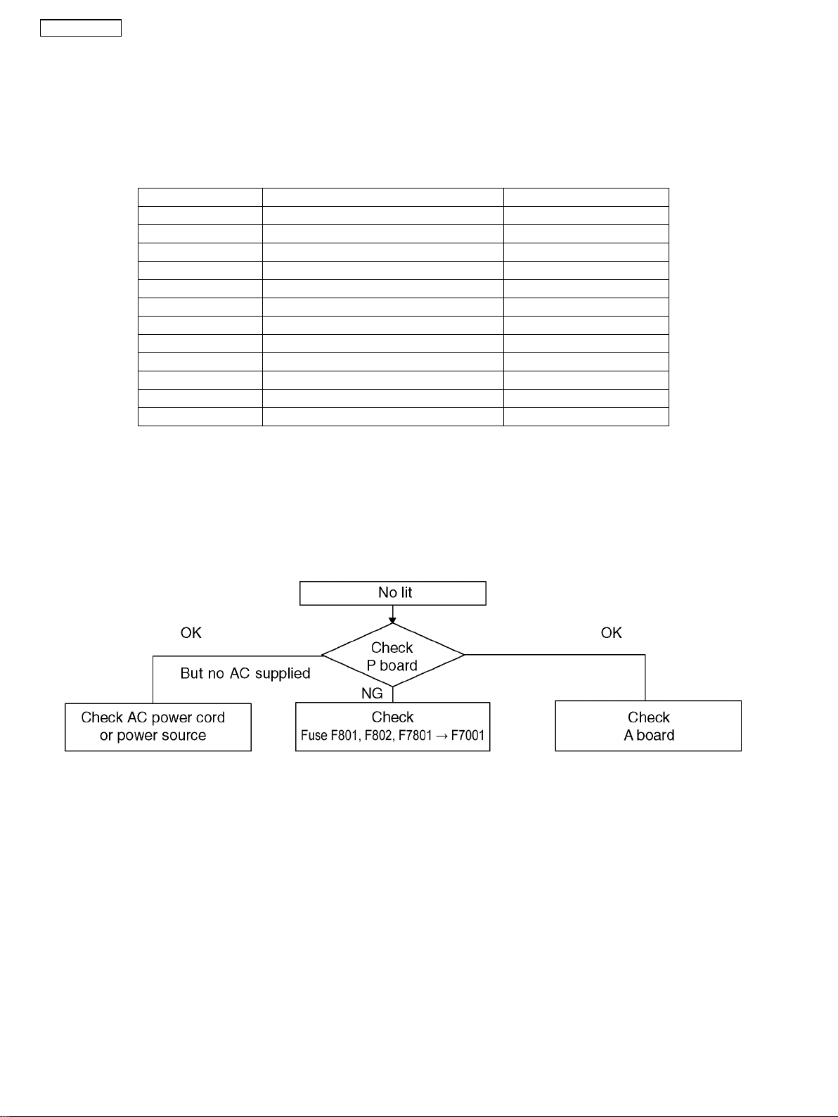
6.3. No Power
First check point
There are following 2 states of No Power indication by power LED.
1. No lit
2. Red is lit then turns red blinking a few seconds later. (See 6.2.)
12
Page 13
7 Disassembly and Assembly Instructions
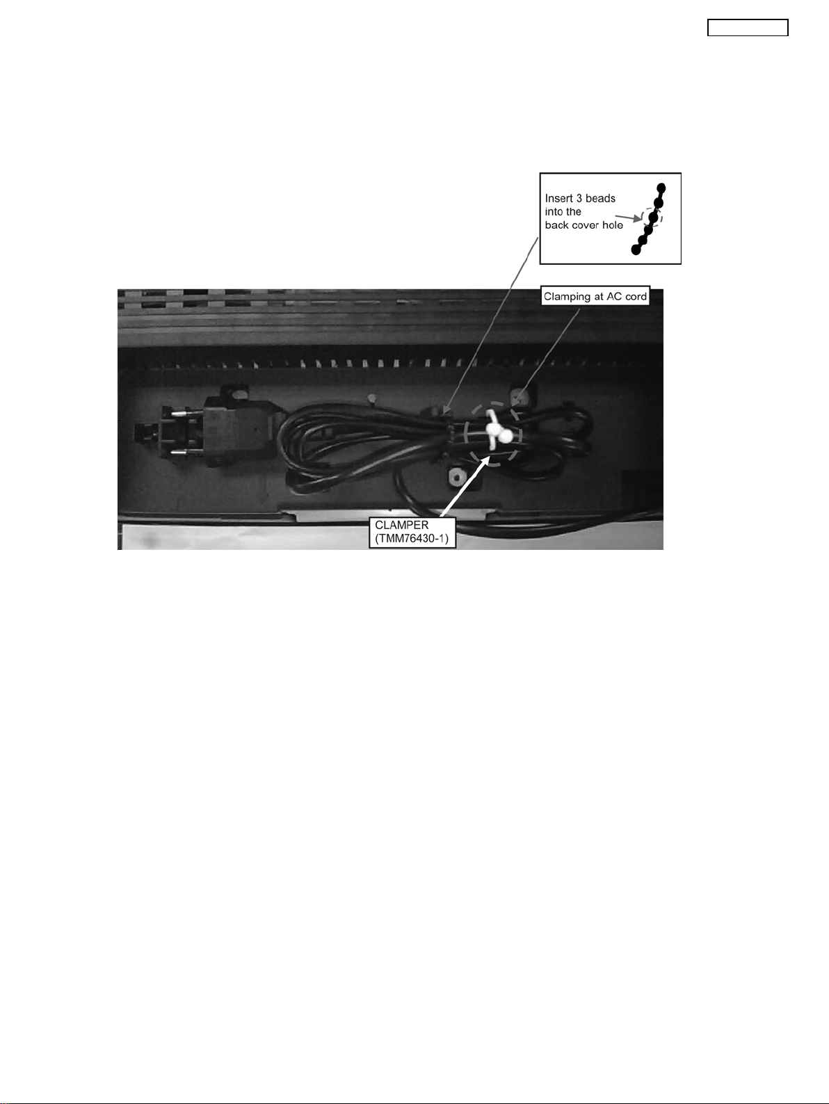
7.1. AC Cord Dressing
1. Clamp plug with clamper.
2. Insert beads 3 pcs. And slide down to lower hole.
TC-L42S20BL
13
Page 14
TC-L42S20BL
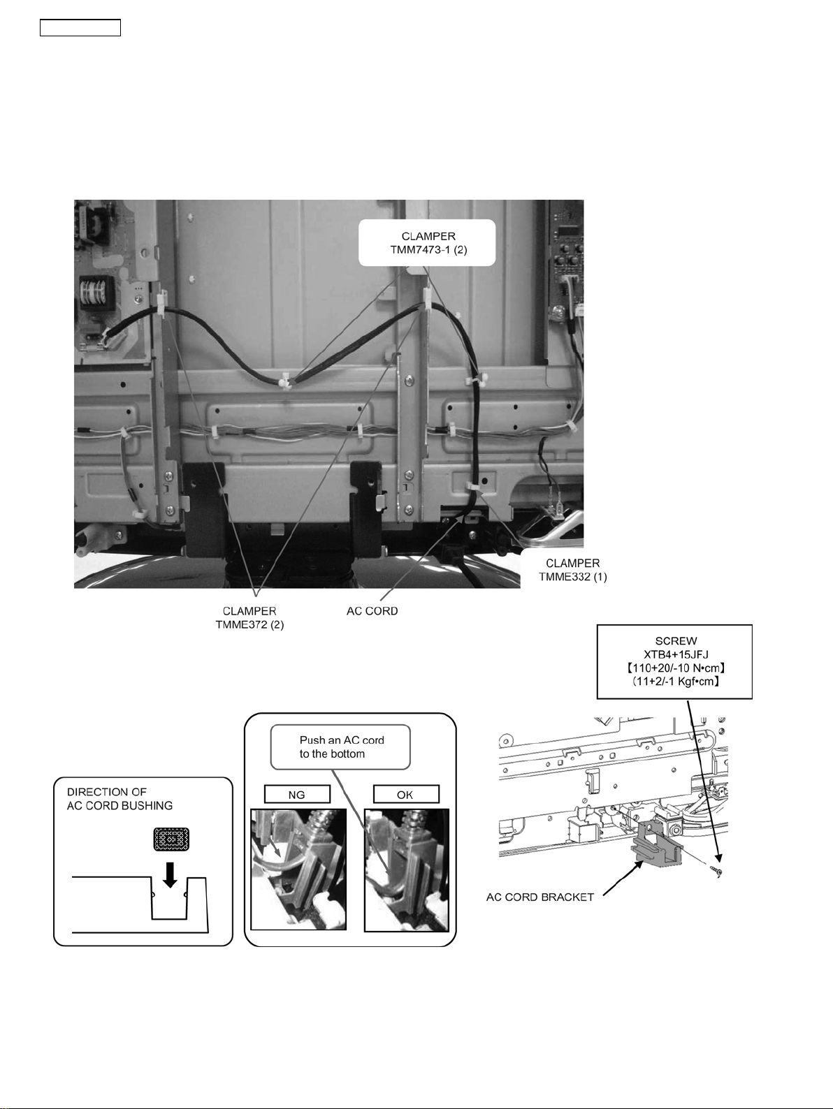
7.2. AC Cord Installation
1. Put on the AC CORD BRACKET on the CABINET.
2. Fix the AC CORD BRACKET with SCREW.
3. Insert AC CORD connector into P-PCB connector.
4. Clamp the AC CORD.
5. Insert AC CORD bushing into the AC CORD BRACKET.
6. AC CORD is pushed into the bottom of the bracket.
14
Page 15
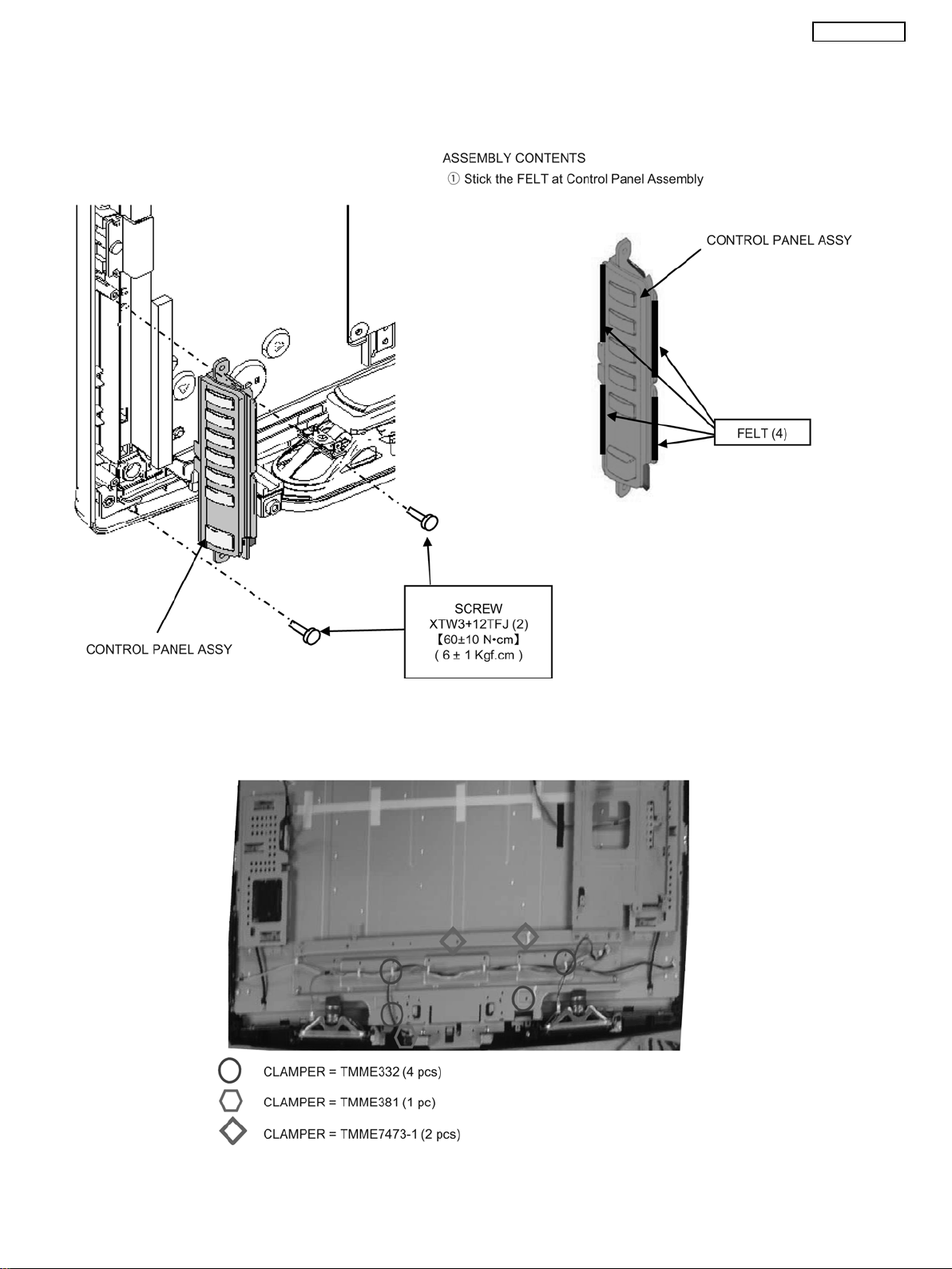
7.3. Control Panel Assembly & Clamper Installation
1. Put control panel Assy on the cabinet.
2. Fix the control panel with screws.
TC-L42S20BL
Fix clamper at bottom mtg.
15
Page 16
TC-L42S20BL
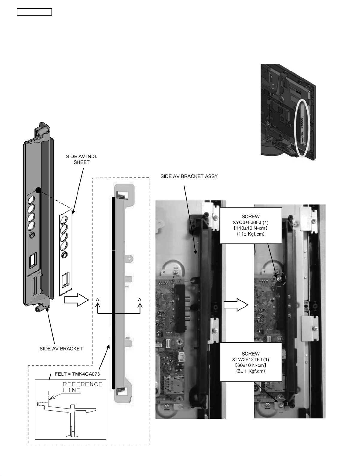
7.4. Side AV Preparation & Installation
1. Stick the side av indi. Sheet and felt on the side av bracket.
2. Insert the SIDE AV BRACKET from the side position of the A-PCB.
3. Fix the SCREW with A-PB-MTG METAL.
16
Page 17
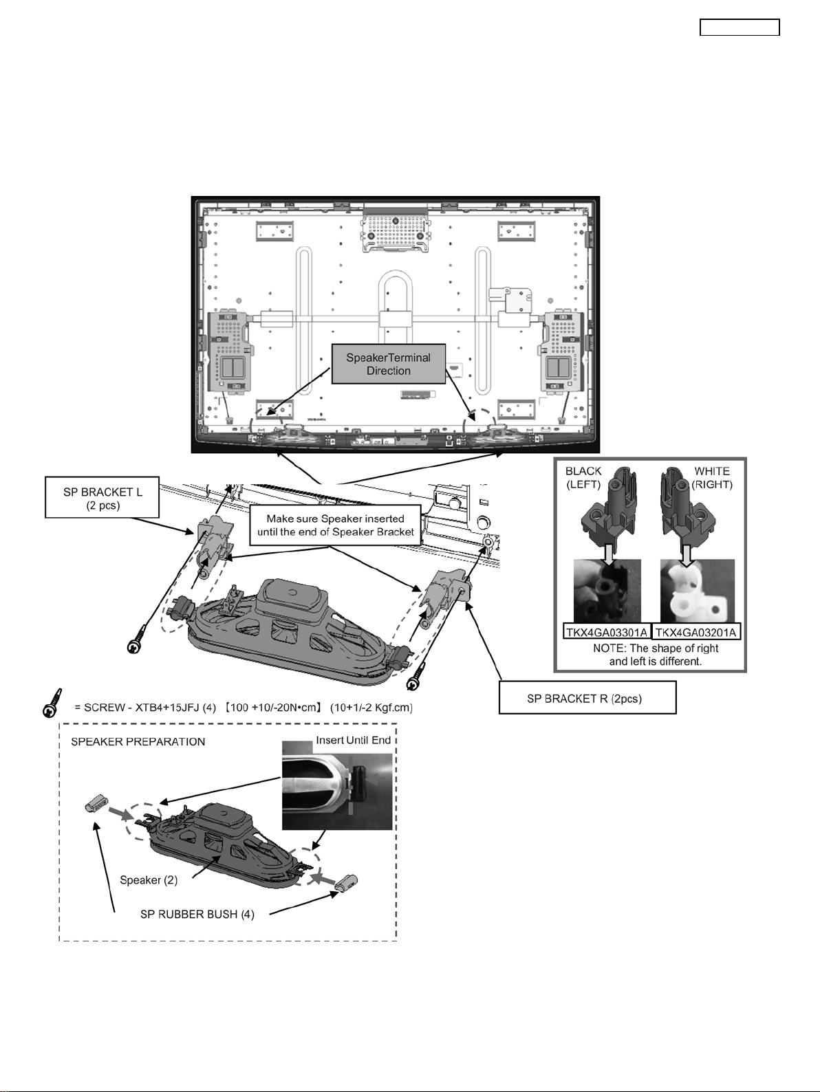
7.5. Speaker Preparation & Installation
1. Stick the SP sponge.
2. SP bracket put on cabinet.
3. Fix them with screws.
4. Insert the SP rubber bush into the SP unit.
5. Stick sponge at speaker.
6. Insert the SP unit to SP bracket.
TC-L42S20BL
17
Page 18
TC-L42S20BL
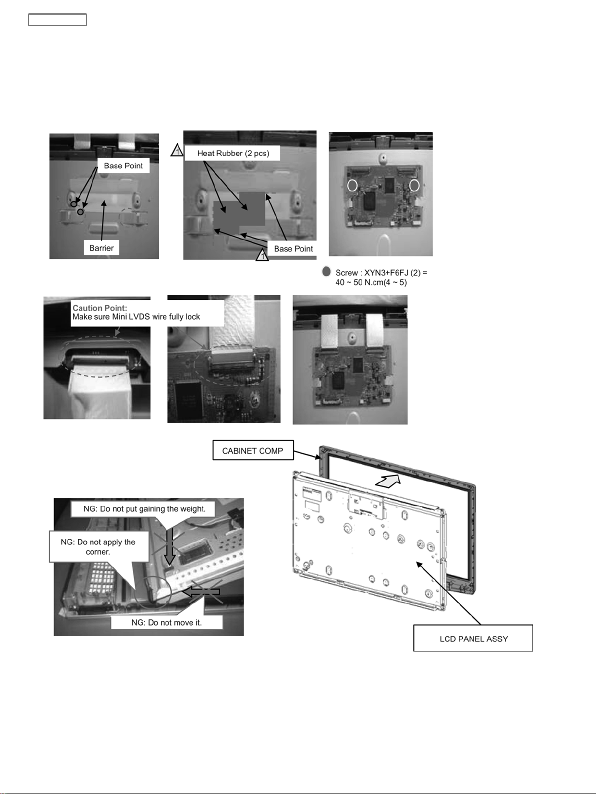
7.6. LCD Panel Assembly Installation
1. Stick barrier at LCD Panel.
2. Stick Heat Rubber at Barrier.
3. Screw inverter board at LCD panel.
4. Slot mini LVDS wire at LCD panel board and inverter board.
5. Put LCD panel on the cabinet.
18
Page 19
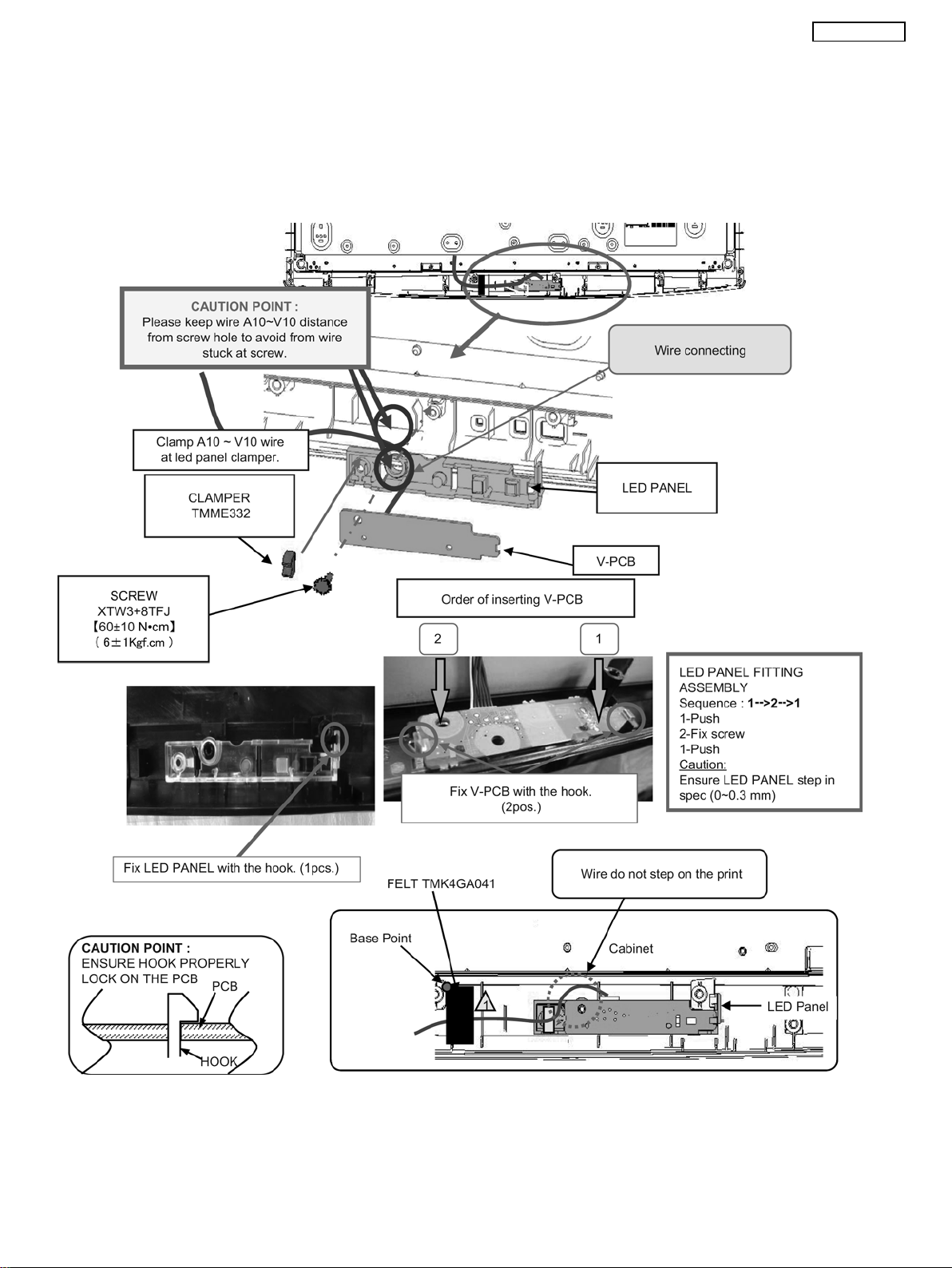
7.7. LED Panel Installation
1. Fix LED PANEL on CABINET.
2. Wire connecting. (V10).
3. Put V-PCB on CABINET.
4. Fix them with SCREW.
5. Insert the CLAMPER.
6. Stick felt at A10-V10 wire.
TC-L42S20BL
19
Page 20
TC-L42S20BL
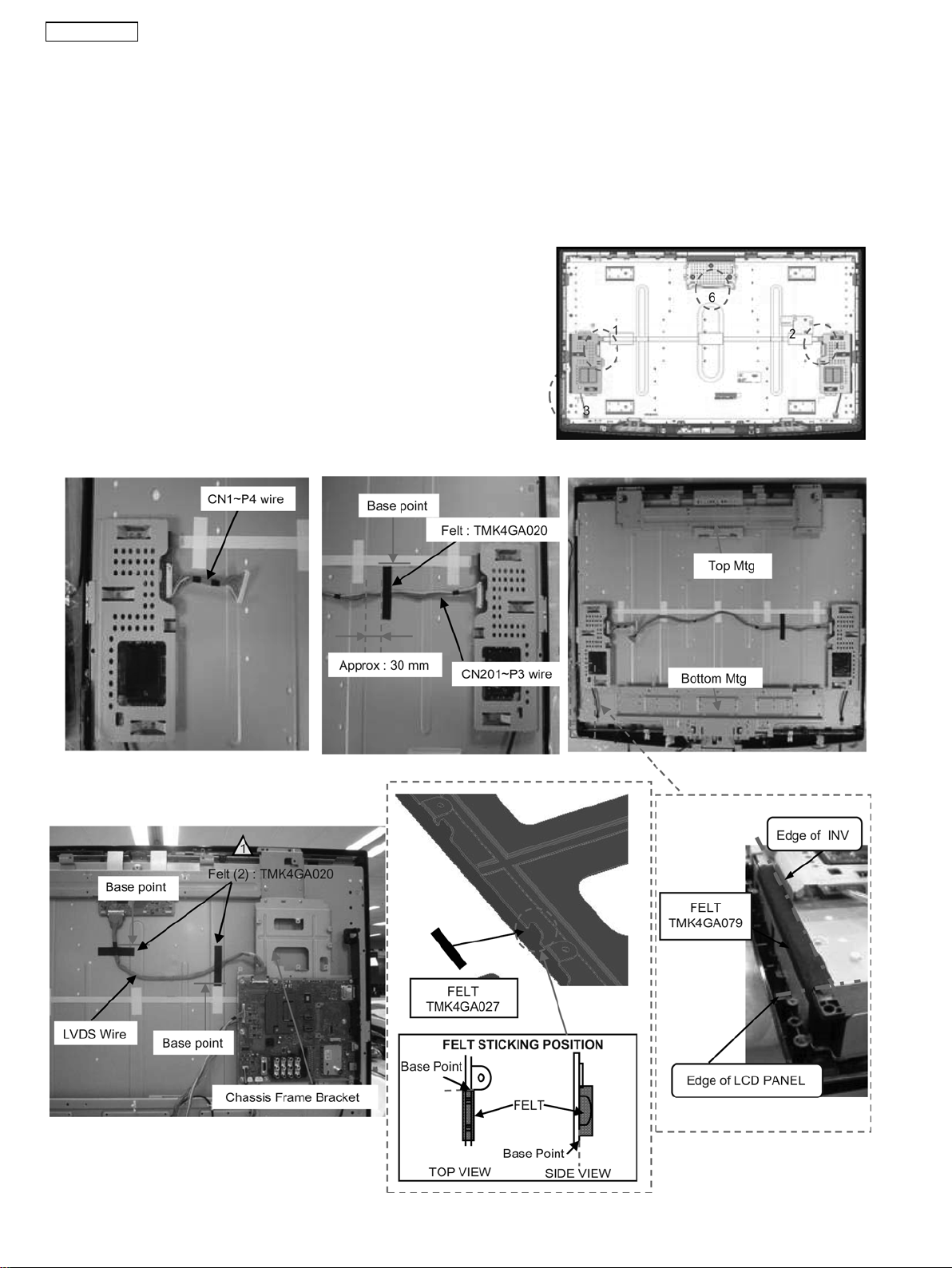
7.8. Felt Sticking at LVDS Wire
1. Insert CN1~P4 wire to inverter.
2. Insert CN201~P3 wire to inverter and stick felt.
3. Stick felt at LCD panel (Bottom left side).
4. Fix Top mtg and Bottom Mtg.
5. Fix Chassis frame bracket at Top Mtg and Bottom Mtg.
6. Insert LVDS wire to inverter and stick 3 felt.
7. Stick left at chassis frame to avoid sharp edge.
20
Page 21
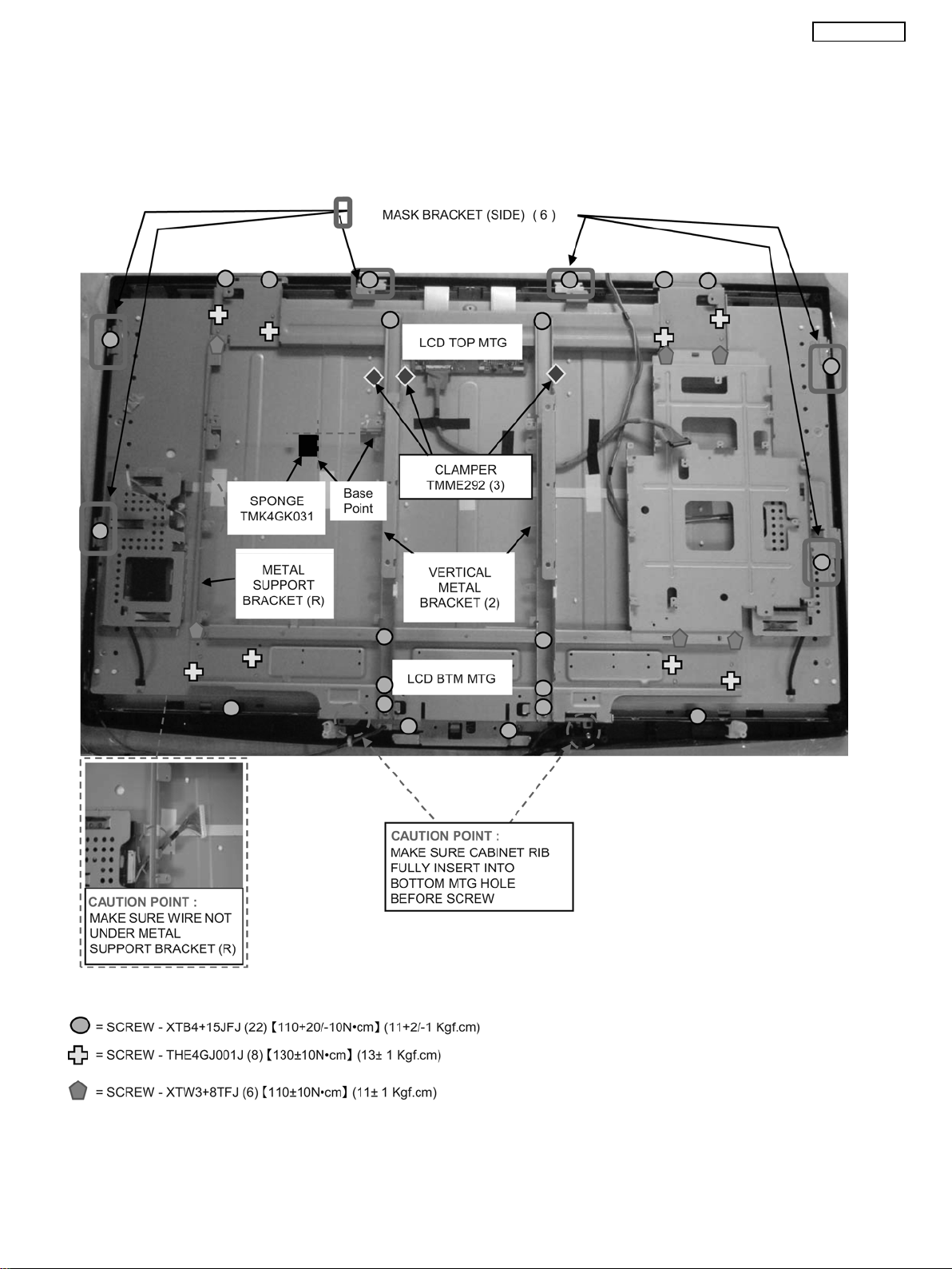
7.9. LCD Bracket and MTG Installation
1. Fix MASK BRACKET (SIDE/TOP/BTM) on the cabinet.
2. Fix Vertical Metal Bracket, Metal Support Bracket (R).
3. Fix them with SCREW.
4. Fix Clamper at Vertical Metal Bracket.
TC-L42S20BL
21
Page 22
TC-L42S20BL
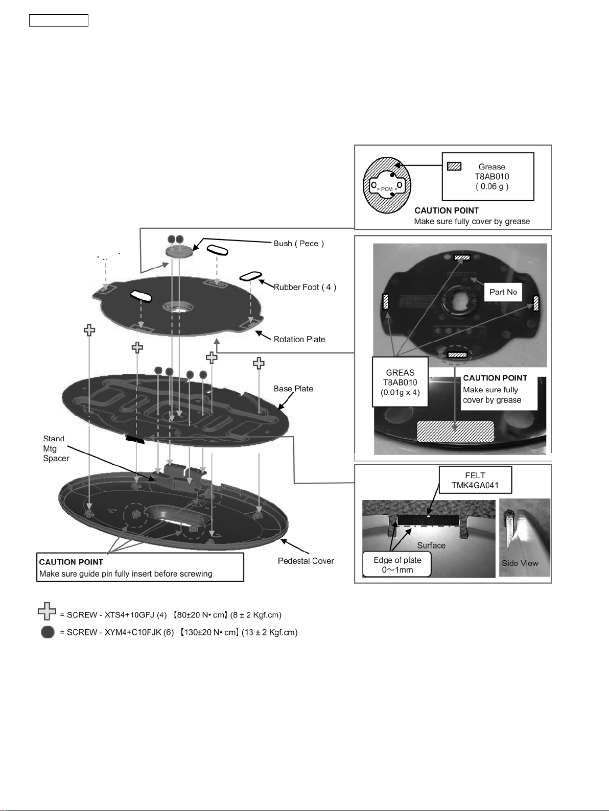
7.10. Pedestal Assembly
1. Fix stand mtg spacer at pedestal cover.
2. Stick felt at front base plate.
3. Fix base plate at stand mtg and pedestal cover and screw.
4. Stick rubber foot at rotation plate.
5. Apply grease at rotation plate and bush (pede).
6. Fix rotation plate and bush (pede) at base plate and screw.
22
Page 23
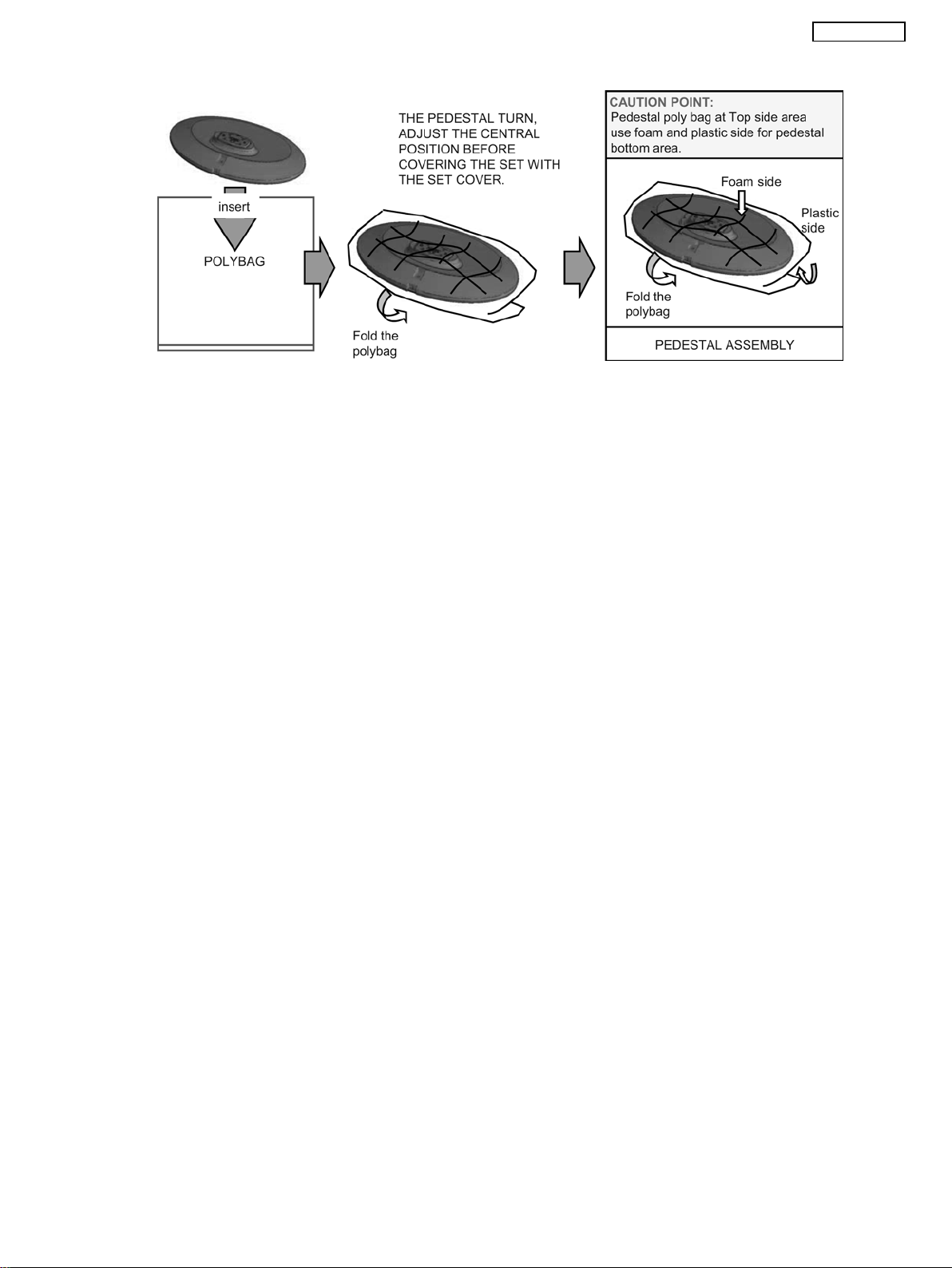
Put Pedestal Assembly into polybag and fold properly.
TC-L42S20BL
23
Page 24
TC-L42S20BL
8 Measurements and Adjustments
8.1. Voltage chart of A-board
Set IP-Board to a dummy set and check the satisfaction with the specified voltage as following table.
Power Supply Name Measurement Point Specification (V)
SUB1.8V TP5601 1.74 - 1.90
SUB1.2V TP5600 1.18 - 1.32
SUB3.3V TP5602 3.19 - 3.46
SUB5V TP5200 4.9 - 5.1
SUB9V TP5220 8.82 - 9.18
STB5V TP5400 4.9 - 5.1
8.2. Voltage chart of P-board
Set IP-Board to a dummy set or dummy load and check the satisfaction with the specified voltage as following table.
Power Supply
Name
P24V TP7503 24 ± 1.2 V NO CARE
17V TP7502 18 ± 2 V NO CARE
DTV12V TP7501 12 ± 0.6 V NO CARE
TUNER6V TP7601 6.1 ± 0.3 V NO CARE
DC390V TP7201 390 ± 10 V NO CARE * HOT
Measurement
Point
Normal Condition
(V)
Stby Condition
(V)
24
Page 25

9 Block Diagram
A-BOARD
9.1. Main Block Diagram
V-BOARD
POWER LED
USB
SLOT
SD CARD
USB DATA
SD CARD DATA
DTV12V
SUB5V
STB5V
ANALOG-ASIC
OVP_DET
POWER LED
STB+3.3V
REMOTE RECEIVER
C.A.T.S. SENSOR
V10
A10
STB+3.3V
SOS DET
C.A.T.S. SENSOR
REMOTE RECEIVER
SOUND17V
DROP
VOLTAGE
D/A
ERROR DET
OVER
VOLTAGE
VREF_1-12
LVDS DATA
VCON31V
VOFF2-6V
DVDD2.5V
AVDD13.7V
TC-L42S20BL
LCD PANEL
A14
PANEL
CONTROL
PANEL
BACK LIGHT
(D Chip)
(A Chip)
TS Parallel
OFDM
IFD_OUT
V
SIF_OUT
DIGITAL SIGNAL PROCESSOR
TUNER
EEPROM
SIF
SD CARD DATA
TS Parallel
SOUND SOS
SOUND SOS
(LED:9TIMES)
(LED:9TIMES)
HDMI I/F
TMDS DATA
TMDS DATA
HDMI1
Peaks sLD
RECEIVER
TMDS DATA
HDMI3
HDMI2
(SIDE)
STB+5.8V
POWER SW
OVP_DET
SUB9V
DCDC
DTV12V
DTV12V
12V
SUB9V
STB5.8V
RELAY
DCDC
SUB3.3V
SUB3.3V
SUB_ON
DCDC
SUB1.8V
SUB1.8V
+5.8VS
A09
P2
SUB1.2V
DCDC
TUNER6V
SUB1.2V
SUB
DVDD2.5V
AVDD13.7V
(LED:3TIMES)
(LED:3TIMES)
DCDC
PANEL POWER SOS
AVDD13.7V
DVDD2.5V
SOUND17V
A02
K01
+5.8VS
ON
32V
17V
STB5V
DCDC
ON/OFF
STB5V
INV_PWM
INVERTER
TUNER5V
DCDC
INV_ON
POWER
+5.8VS
TUNER5V
INV_SOS
CONTROL
CURCUIT
DCDC
SUB5V
SUB5V
P5,P6.P7,P8
STB3.3V
STB3.3V
(STM)
STB_RESET
STB_RESET
A/D
L/R
EEPROM
AUDIO
PROCESSOR
D/A
CONVERTOR
DTV_L/R
CONVERTOR
Y/PB/PR,
R/G/B/H/V CVBS
REMOTE IN
POWER LED(R)
C.A.T.S. SENSOR
VIDEO
PROCESSOR
DVB_CVBS
SUB 3.3V SENSE
(LED:7TIMES)
(LED:7TIMES)
(LED:3TIMES)
(LED:3TIMES)
DTV12V SENSE
(LED:4TIMES)
(LED:4TIMES)
(LED:1TIMES)
(LED:1TIMES)
CPU BUS
I/F
NAND
FLASH
CPU BUS
PWM
HP
PANEL POWER SOS
INV_SOS
INV_ON
SUB_ON
KEYSCAN
INV_PWM
(DAC_ENB)
HOT START
INV_SOS
INV_ON
INV_PWM
LVDS DATA
OPERATION
BUTTON
AV SW
CONTROL PANEL
V
MONITOR L,R
V/Y/PB/PR
L/R
V
AV1
MONITOR V
L/R
L/R
V
R/G/B/H/V
PC
AV2
AV3
MONITOR
OUT
(SIDE)
PWM
L
HEADPHONE
(SIDE)
SPEAKER(L)
AUDIO
A12
SOS DET
AMP
R
SPEAKER(R)
K-BOARD
P-BOARD
POWER SUPPLY
RECTIFIER
PROCESS
VOLTAGE
RECTIFIER
POWER
CONTROL
PFC
CONTROL
STANDBY
VOLTAGE
RECTIFIER
RECTIFIER
AC CORD
NEUTRAL
P1
LINE
FILTER
LIVE
25
Page 26
TC-L42S20BL
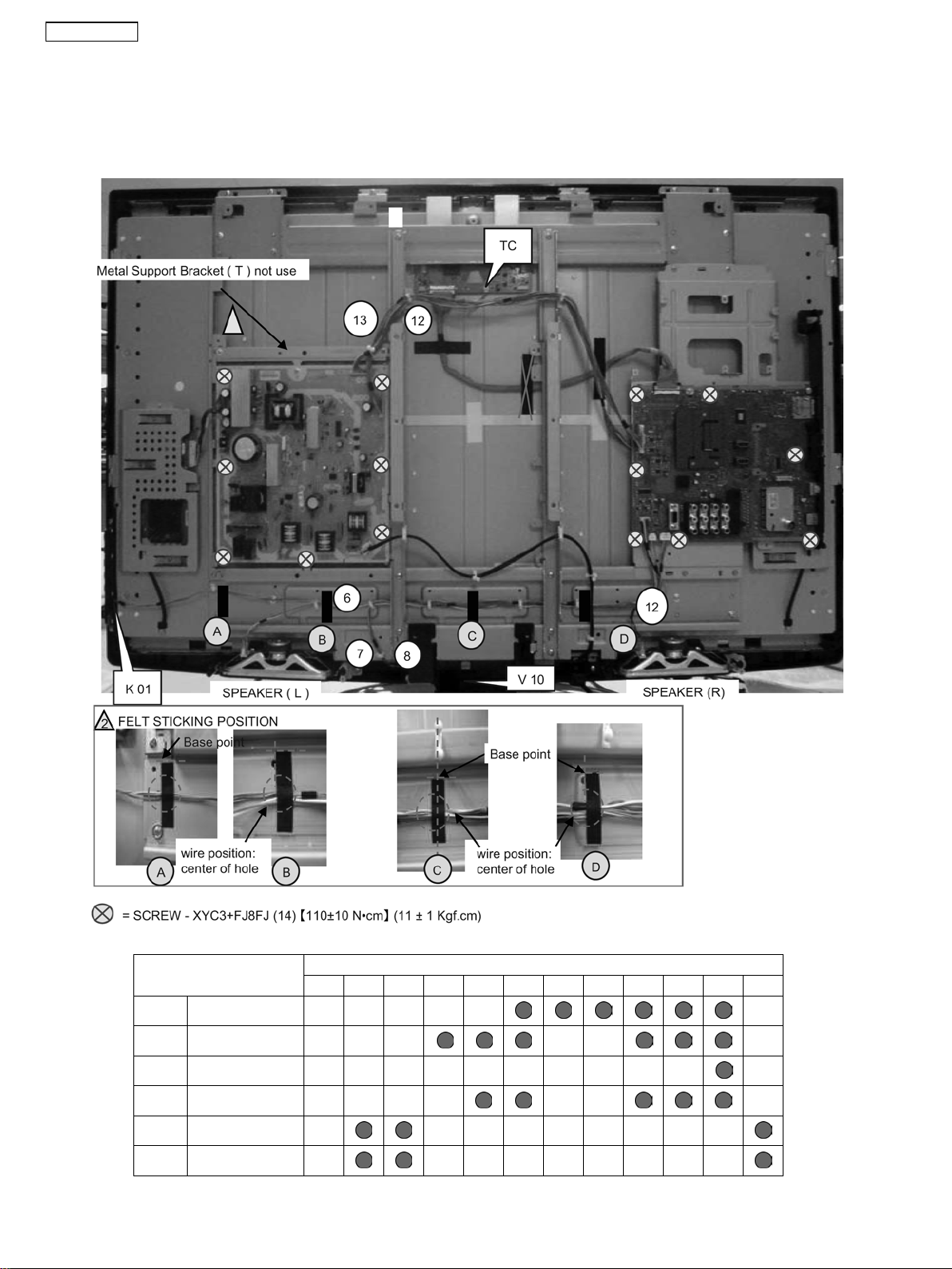
10 Wiring Connection Diagram
1. Fix PCB at chassis frame and mtg and screw.
2. Wiring No.1~No.6.
3. Remove dust of terminal of LVDS and PB connector. (by ion blow)
Wire
No.1 A10 - V10
No.2 A04 - K01
No.3 A11 - SP (R)
No.4 A11 - SP (L)
No.5 INV (CN 201) ~ P3
No.6 A3 ~ P2
Clamper
1 2 3 A B 6 7 8 C D 12 13
26
Page 27
11 Schematic Diagram
11.1. Schematic Diagram Notes
TC-L42S20BL
27
Page 28
TC-L42S20BL
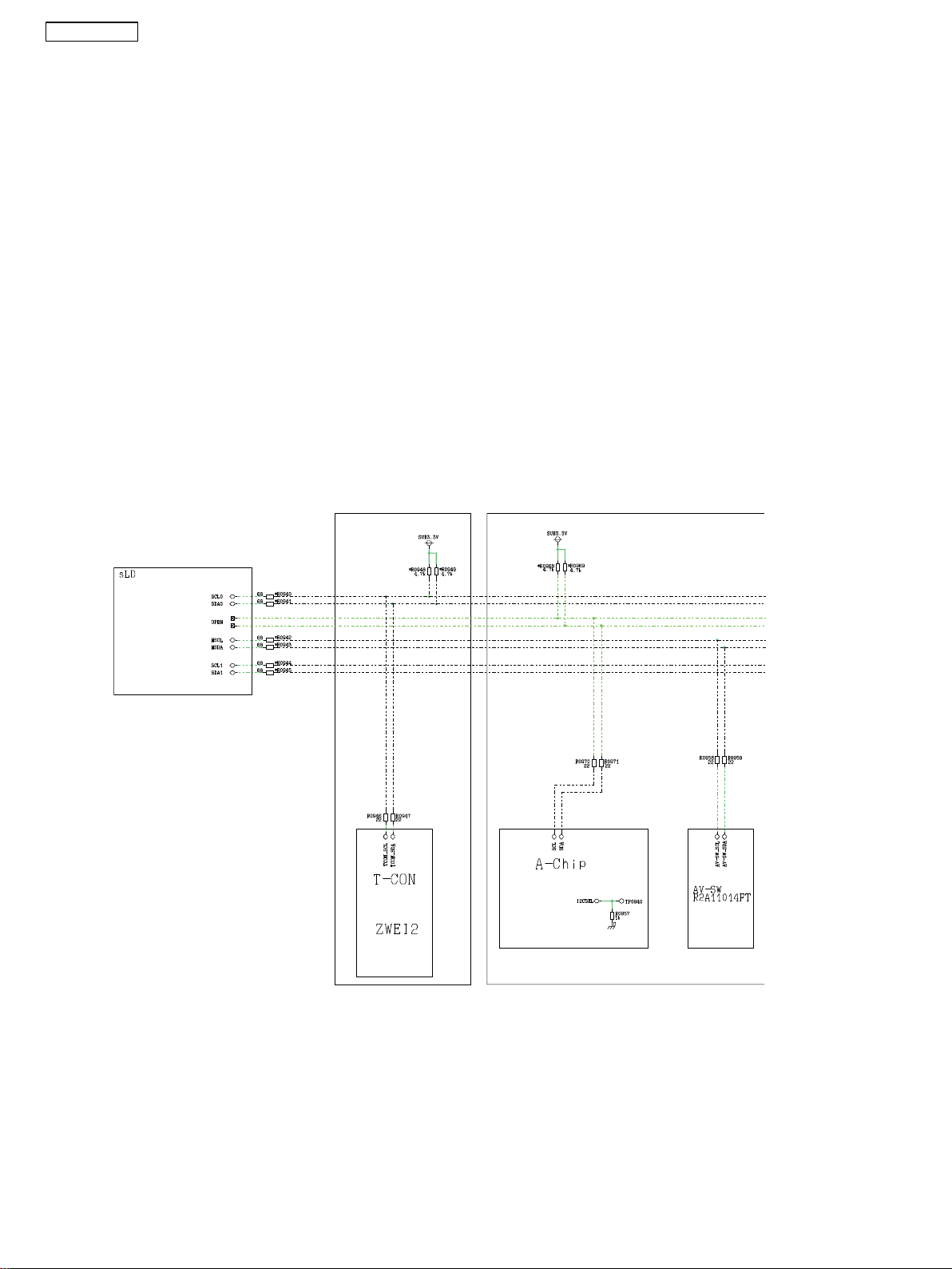
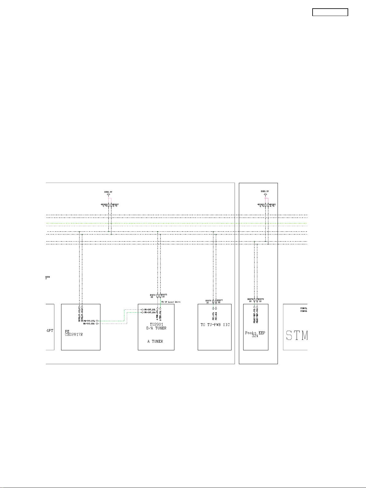
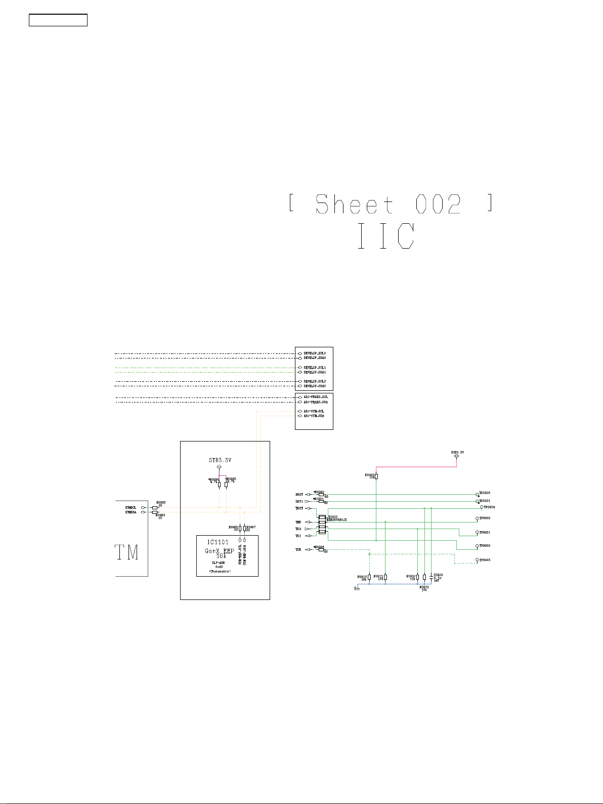
11.2. A Board
11.2.1. A Board - Sheet : 002 (1 / 3)
<1A>
28
<2A>
Page 29
11.2.2. A Board - Sheet : 002 (2 / 3)
<1A>
TC-L42S20BL
<2A>
<1B>
<2B>
<3B>
29
Page 30
TC-L42S20BL
11.2.3. A Board - Sheet : 002 (3 / 3)
<1B>
<2B>
<3B>
30
Page 31

11.2.4. A Board - Sheet : 010 (1 / 3)
TC-L42S20BL
<1A>
31
<2A>
<3A>
Page 32

TC-L42S20BL
11.2.5. A Board - Sheet : 010 (2 / 3)
<1A>
<1B>
<2A>
<3A>
<2B>
<3B>
32
Page 33

11.2.6. A Board - Sheet : 010 (3 / 3)
<1B>
TC-L42S20BL
<2B>
<3B>
33
Page 34

TC-L42S20BL
11.2.7. A Board - Sheet : 011 (1 / 3)
<1A>
34
<2A>
Page 35

11.2.8. A Board - Sheet : 011 (2 / 3)
<1A>
TC-L42S20BL
<1B>
<2B>
<2A>
<3B>
35
Page 36

TC-L42S20BL
11.2.9. A Board - Sheet : 011 (3 / 3)
<1B>
<2B>
<3B>
36
Page 37

11.2.10. A Board - Sheet : 012 (1 / 3)
TC-L42S20BL
<1A>
<2A>
37
<3A>
Page 38

TC-L42S20BL
11.2.11. A Board - Sheet : 012 (2 / 3)
<1B>
<1A>
<2A>
<3A>
<2B>
38
Page 39

11.2.12. A Board - Sheet : 012 (3 / 3)
<1B>
TC-L42S20BL
<2B>
39
Page 40

TC-L42S20BL
11.2.13. A Board - Sheet : 020 (1 / 3)
<1A>
40
<2A>
Page 41

11.2.14. A Board - Sheet : 020 (2 / 3)
<1A>
<2A>
TC-L42S20BL
<1B>
<2B>
<3B>
41
Page 42

TC-L42S20BL
11.2.15. A Board - Sheet : 020 (3 / 3)
<1B>
<2B>
<3B>
42
Page 43

11.2.16. A Board - Sheet : 031 (1 / 3)
TC-L42S20BL
<1A>
43
<2A>
Page 44

TC-L42S20BL
11.2.17. A Board - Sheet : 031 (2 / 3)
<1A>
<1B>
<2A>
<2B>
<3B>
<4B>
44
Page 45

11.2.18. A Board - Sheet : 031 (3 / 3)
<1B>
TC-L42S20BL
<2B>
<3B>
<4B>
45
Page 46

TC-L42S20BL
11.2.19. A Board - Sheet : 033 (1 / 2)
<1A>
<2A>
46
Page 47

11.2.20. A Board - Sheet : 033 (2 / 2)
<1A>
TC-L42S20BL
<2A>
47
Page 48

TC-L42S20BL
11.2.21. A Board - Sheet : 040 (1 / 5)
<1A>
48
<2A>
Page 49

11.2.22. A Board - Sheet : 040 (2 / 5)
TC-L42S20BL
<1A>
<1B>
<2A>
<2B>
49
Page 50

TC-L42S20BL
11.2.23. A Board - Sheet : 040 (3 / 5)
<1B>
<1C>
<2B>
<2C>
50
Page 51

11.2.24. A Board - Sheet : 040 (4 / 5)
<1D>
<2D>
<1C>
TC-L42S20BL
<2C>
51
Page 52

TC-L42S20BL
11.2.25. A Board - Sheet : 040 (5 / 5)
<1D>
<2D>
52
Page 53

11.2.26. A Board - Sheet : 050 (1 / 2)
TC-L42S20BL
<1A>
53
<2A>
Page 54

TC-L42S20BL
11.2.27. A Board - Sheet : 050 (2 / 2)
<1A>
<2A>
54
Page 55

11.2.28. A Board - Sheet : 060 (1 / 2)
TC-L42S20BL
<1A>
55
<2A>
Page 56

TC-L42S20BL
11.2.29. A Board - Sheet : 060 (2 / 2)
<1A>
<2A>
56
Page 57

11.2.30. A Board - Sheet : 061 (1 / 1)
TC-L42S20BL
57
Page 58

TC-L42S20BL
11.2.31. A Board - Sheet : 090 (1 / 3)
<1A>
<2A>
58
Page 59

11.2.32. A Board - Sheet : 090 (2 / 3)
TC-L42S20BL
<1A>
<2A>
<1B>
<2B>
59
Page 60

TC-L42S20BL
11.2.33. A Board - Sheet : 090 (3 / 3)
<1B>
<2B>
60
Page 61

11.2.34. A Board - Sheet : 201 (1 / 3)
TC-L42S20BL
<1A>
<2A>
<3A>
<4A>
61
Page 62

TC-L42S20BL
11.2.35. A Board - Sheet : 201 (2 / 3)
<1A>
<2A>
<3A>
<4A>
<1B>
<2B>
62
Page 63

11.2.36. A Board - Sheet : 201 (3 / 3)
TC-L42S20BL
<1B>
<2B>
63
Page 64

TC-L42S20BL
11.2.37. A Board - Sheet : 300 (1 / 4)
<1A>
<2A>
64
Page 65

11.2.38. A Board - Sheet : 300 (2 / 4)
TC-L42S20BL
<1B>
<1A>
<2A>
65
<2B>
Page 66

TC-L42S20BL
11.2.39. A Board - Sheet : 300 (3 / 4)
<1B>
<1C>
<2B>
<2C>
66
Page 67

11.2.40. A Board - Sheet : 300 (4 / 4)
<1C>
TC-L42S20BL
<2C>
67
Page 68

TC-L42S20BL
11.2.41. A Board - Sheet : 700 (1 / 2)
<1A>
68
<2A>
Page 69

11.2.42. A Board - Sheet : 700 (2 / 2)
<1A>
TC-L42S20BL
<2A>
69
Page 70

TC-L42S20BL
<1A>
<2A>
11.2.43. A Board - Sheet : 701 (1 / 2)
70
Page 71

11.2.44. A Board - Sheet : 701 (2 / 2)
<1A>
TC-L42S20BL
<2A>
71
Page 72

TC-L42S20BL
11.3. K Board
11.3.1. K Board (1 / 2)
72
Page 73

11.3.2. K Board (2 / 2)
TC-L42S20BL
73
Page 74

TC-L42S20BL
11.4. P Board
11.4.1. P Board (1 / 3)
<1A>
<2A>
74
<3A>
<4A>
Page 75

11.4.2. P Board (2 / 3)
<1A>
<2A>
TC-L42S20BL
<1B>
<3A>
<4A>
<2B>
<3B>
<4B>
75
Page 76

TC-L42S20BL
11.4.3. P Board (3 / 3)
<1B>
<2B>
<3B>
<4B>
76
Page 77

11.5. V Board
11.5.1. V Board (1 / 3)
TC-L42S20BL
77
Page 78

TC-L42S20BL
11.5.2. V Board (2 / 3)
78
Page 79

11.5.3. V Board (3 / 3)
TC-L42S20BL
79
Page 80

TC-L42S20BL
12 Printed Circuit Board
12.1. A-Board
A-Board (A Side)
TNP4G468
1
A
B
C
D
E
F
G
2 3 4 5 6 7 8 9 10
H
I
J
K
L
M
Parts Location
Ref. No Location Ref. No Location Ref. No Location Ref. No Location
IC2950 K10 IC3902 E6 IC8200 G2 IC8851 L8
IC2951 I10 IC3903 G5 IC8300 K8 IC8852 K2
IC2952 J9 IC5600 B4 IC8301 L9 IC9980 L4
IC3000 E9 IC5601 B6 IC8302 L9 IC8950 I2
IC3900 H7 IC5603 G5 IC8400 K4 D3300 D7
IC3901 G7 IC5604 G4 IC8401 G3
80
Page 81

12.2. A-Board
1
2 3 4 5 6 7 8 9 10
A-Board (B Side)
TNP4G468
A
B
C
D
E
F
TC-L42S20BL
G
H
I
J
K
L
M
Parts Location
Ref. No Location Ref. No Location Ref. No Location Ref. No Location
IC1101 H4 IC4801 A9 IC5220 B1 D3300 D4
IC2301 B4 IC4802 A8 IC5416 A2
IC3350 L4 IC4803 D6 IC8001 F7
IC3904 G4 IC4804 D10 IC8402 J7
IC3905 F4 IC5000 K6 IC8921 H9
IC4800 G10 IC5200 B2
81
Page 82

TC-L42S20BL
12.7. P-Board
P-Board (A Side)
1
2 3 4 5 6 7 8 9 10
12.3. P-Board
TNP4G478
A
B
C
D
E
F
G
H
I
J
Parts Location
Ref. No Location Ref. No Location Ref. No Location Ref. No Location
IC7201 F5 D7002 H6 D7310 E4 D7420 H5
IC7301 D3 D7102 I8 D7311 E3 D7501 B7
IC7401 F4 D7204 G9 D7312 E3 D7503 C8
IC7501 D1 D7208 E5 D7313 C4 D7504 E9
IC7601 E1 D7207 H7 D7314 D3 D7518 A8
D7209 F6 D7315 C5 D7601 E1
D7210 F3 D7323 E3 D7602 F1
D7301 D4 D7401 H5 D7603 F2
D7302 D4 D7402 G4 D7701 D1
D7303 D3 D7403 F4 D7702 J8
D7304 D4 D7404 F3 D7704 E3
D7305 C4 D7405 G5 D7705 E3
D7306 C4 D7406 G5 D7753 E3
D7307 D4 D7407 D6 D7889 B1
D7308 E4 D7408 G3
D7309 E4 D7409 E3
82
Page 83

12.8. P-Board
P-Board (B Side)
1
2 3 4 5 6 7 8 9 10
12.4. P-Board
TNP4G478
A
B
C
D
E
F
TC-L42S20BL
G
H
I
J
Parts Location
Ref. No Location Ref. No Location Ref. No Location Ref. No Location
IC7301 D8 D7001 I9 D7306 C7 D7407 G5
IC7401 F7 D7002 H5 D7307 D7 D7408 G8
D7102 I2 D7314 D8 D7420 H6
D7204 G2 D7323 E8 D7501 B4
D7207 H5 D7401 H6 D7503 C3
D7208 E6 D7402 G8 D7504 D1
D7209 F6 D7403 F8 D7518 A3
D7210 E8 D7404 F8 D7601 E10
D7301 D7 D7405 G6 D7602 F10
D7302 C7 D7406 G6 D7603 F9
83
Page 84

TC-L42S20BL
13 Exploded View and Replacement Parts List
13.1. Exploded View and Mechanical Replacement Parts List
Please click the radio button for ‘Diagrams ll/Parts List’ on the menu bar.
13.2. Electrical Replacement Parts List
13.2.1. Replacement Parts List Notes
84
Page 85

13.2.2. Mechanical Parts Location
TC-L42S20BL
3
SAP
TV/AV
SUBMENU
R-TUNE
SLEEP
7
13.2.3. Mechanical Replacement Parts List 13.2.4. Assembled Boards
REF. NO. PART NO. PART NAME & DESCRIPTION
1 L0AA14B00006 FULL RANGE SPEAKER 10W 8Ω
2 L5EDDAT00008 LCD DISPLAY
3 TNQ2B5304 REMOTE CONTROL UNIT
4 TBL4GA0045 PEDESTAL ASSEMBLY
5 TTU2BQFW REAR COVER
6 TXFKY010QKV CABINET COMPLETE ASSEMBLY
7 K2CQ2YY00070 AC CORD K2DR42E00007 - AC ADAPTER
REF. NO. PART NO. PART NAME & DESCRIPTION
PCB1 TNP4G468GL A BOARD
PCB2 TNP4G478AG P BOARD
PCB3 TNPA5243AA K BOARD
PCB4 TNPA5275AA V BOARD
85
Page 86

TC-L42S20BL
13.2.5. Packing Exploded View 1
86
Page 87

13.2.6. Packing Exploded View 2
TC-L42S20BL
87
Page 88

TC-L42S20BL
13.2.7. Electrical Replacement Parts List
REF. NO. PART NO. PART NAME & DESCRIPTION
CAPACITORS
C0900 F1G1C104A116 CERAMIC CAP. SMD 100 nF 16V 10%
C1041 F1G1H102A730 CERAMIC CAP. SMD 1 nF 50V 10%
C1042 F1G1H102A730 CERAMIC CAP. SMD 1 nF 50V 10%
C1043 F1G1H102A730 CERAMIC CAP. SMD 1 nF 50V 10%
C1100 F1G1E103A123 CERAMIC CAP. SMD 10 nF 25V 10%
C1101 F1H1H103A970 CERAMIC CAP. SMD 10 nF 50V 10%
C1102 F1G1C104A116 CERAMIC CAP. SMD 100 nF 16V 10%
C2055 F1J1A106A087 CERAMIC CAP. SMD 10 µF 10V 10%
C2057 F1J1A106A087 CERAMIC CAP. SMD 10 µF 10V 10%
C2071 EEEHB0J101UR ELECTROLYTIC SMD 100 µF 6,3 V 20%
C2072 EEEHB0J101UR ELECTROLYTIC SMD 100 µF 6,3 V 20%
C2104 F1G1H100A731 CERAMIC CAP. SMD 10 PF 50V 5%
C2107 F1G1A105A047 CERAMIC CAP. SMD 1 µF 10V 10%
C2108 F1G1A105A047 CERAMIC CAP. SMD 1 µF 10V 10%
C2110 F1G1C104A116 CERAMIC CAP. SMD 100 nF 16V 10%
C2311 F1K1E106A136 CERAMIC CAP. SMD 10 µF 25V 10%
C2314 F1J1E105A231 CERAMIC CAP. SMD 1 µF 25V 10%
C2315 F1K1E106A136 CERAMIC CAP. SMD 10 µF 25V 10%
C2316 F1H1H104A970 CERAMIC CAP. SMD 100 nF 50V 10%
C2317 F1J1E105A231 CERAMIC CAP. SMD 1 µF 25V 10%
C2318 F1H1H104A970 CERAMIC CAP. SMD 100 nF 50V 10%
C2320 F1J1E105A231 CERAMIC CAP. SMD 1 µF 25V 10%
C2321 F1H1H104A970 CERAMIC CAP. SMD 100 nF 50V 10%
C2323 F1H1H104A970 CERAMIC CAP. SMD 100 nF 50V 10%
C2324 F1J1E105A231 CERAMIC CAP. SMD 1 µF 25V 10%
C2334 F1J1H474A757 CERAMIC CAP. SMD 0,47 µF 50V 10%
C2335 F1H1E104A129 CERAMIC CAP. SMD 100 nF 25V
C2336 F1H1E104A129 CERAMIC CAP. SMD 100 nF 25V
C2337 F1J1H474A757 CERAMIC CAP. SMD 0,47 µF 50V 10%
C2338 F1H1E104A129 CERAMIC CAP. SMD 100 nF 25V
C2339 F1H1E104A129 CERAMIC CAP. SMD 100 nF 25V
C2340 F1H1H223A970 CERAMIC CAP. SMD 22 nF 50V 10%
C2341 F1H1H223A970 CERAMIC CAP. SMD 22 nF 50V 10%
C2342 F1H1H223A970 CERAMIC CAP. SMD 22 nF 50V 10%
C2343 F1H1H223A970 CERAMIC CAP. SMD 22 nF 50V 10%
C2344 F1H1H223A970 CERAMIC CAP. SMD 22 nF 50V 10%
C2345 F1H1H223A970 CERAMIC CAP. SMD 22 nF 50V 10%
C2346 F1H1H223A970 CERAMIC CAP. SMD 22 nF 50V 10%
C2347 F1H1H223A970 CERAMIC CAP. SMD 22 nF 50V 10%
C2349 F1G1H102A730 CERAMIC CAP. SMD 1 nF 50V 10%
C2351 F1G1H102A730 CERAMIC CAP. SMD 1 nF 50V 10%
C2353 F1G1H102A730 CERAMIC CAP. SMD 1 nF 50V 10%
C2355 F1G1H102A730 CERAMIC CAP. SMD 1 nF 50V 10%
C2501 F2G0J470A019 ELECTROLYTIC SMD 47 µF 6,3 V 20%
C2502 F1G1C103A116 CERAMIC CAP. SMD 10 nF 16V 10%
C2505 F1H1C104A143 CERAMIC CAP. SMD 100 nF 16V 10%
C2514 F1J1A106A087 CERAMIC CAP. SMD 10 µF 10V 10%
C2750 F1G1C104A116 CERAMIC CAP. SMD 100 nF 16V 10%
C2751 F1G1H102A730 CERAMIC CAP. SMD 1 nF 50V 10%
C2752 F1G1H102A730 CERAMIC CAP. SMD 1 nF 50V 10%
C2753 F1G1H102A730 CERAMIC CAP. SMD 1 nF 50V 10%
C2754 F1G1H102A730 CERAMIC CAP. SMD 1 nF 50V 10%
C2755 F1G1H102A730 CERAMIC CAP. SMD 1 nF 50V 10%
REF. NO. PART NO. PART NAME & DESCRIPTION
C2756 F1G1H102A730 CERAMIC CAP. SMD 1 nF 50V 10%
C2757 F1G1H102A730 CERAMIC CAP. SMD 1 nF 50V 10%
C2761 F1G1C104A116 CERAMIC CAP. SMD 100 nF 16V 10%
C2762 F1G1H102A730 CERAMIC CAP. SMD 1 nF 50V 10%
C2775 F1G1H101A731 CERAMIC CAP. SMD 100 PF 50V 5%
C2776 F1G1H102A730 CERAMIC CAP. SMD 1 nF 50V 10%
C2778 F1G1C104A116 CERAMIC CAP. SMD 100 nF 16V 10%
C2779 F1K1C106A126 CERAMIC CAP. SMD 10 µF 16V 10%
C2780 F1H1E104A129 CERAMIC CAP. SMD 100 nF 25V
C2789 F1G1C104A116 CERAMIC CAP. SMD 100 nF 16V 10%
C2905 F2H1A101A009 ELECTROLYTIC SMD 100 µF 10V 20%
C2907 F1G1C104A116 CERAMIC CAP. SMD 100 nF 16V 10%
C2909 F1G1C104A116 CERAMIC CAP. SMD 100 nF 16V 10%
C2910 F1G1C104A116 CERAMIC CAP. SMD 100 nF 16V 10%
C2911 F1G1C104A116 CERAMIC CAP. SMD 100 nF 16V 10%
C2916 F1G1H102A730 CERAMIC CAP. SMD 1 nF 50V 10%
C2917 F1G1C104A116 CERAMIC CAP. SMD 100 nF 16V 10%
C2950 F1J0J4750004 CAP. SMD 4,70 µF 6,3 V 10%
C2951 F1J0J4750004 CAP. SMD 4,70 µF 6,3 V 10%
C2961 F1H1A105A025 CERAMIC CAP. SMD 1 µF 10V 10%
C3003 F1G1C104A116 CERAMIC CAP. SMD 100 nF 16V 10%
C3004 F1G1C104A116 CERAMIC CAP. SMD 100 nF 16V 10%
C3011 F1J1A106A087 CERAMIC CAP. SMD 10 µF 10V 10%
C3015 F1J1A106A087 CERAMIC CAP. SMD 10 µF 10V 10%
C3016 F1G1C104A116 CERAMIC CAP. SMD 100 nF 16V 10%
C3018 F1G1C104A116 CERAMIC CAP. SMD 100 nF 16V 10%
C3019 F1G1C104A116 CERAMIC CAP. SMD 100 nF 16V 10%
C3022 F1H1A105A025 CERAMIC CAP. SMD 1 µF 10V 10%
C3023 F1H1A105A025 CERAMIC CAP. SMD 1 µF 10V 10%
C3024 F1J1A106A087 CERAMIC CAP. SMD 10 µF 10V 10%
C3025 F1J1A106A087 CERAMIC CAP. SMD 10 µF 10V 10%
C3026 F1J1A106A087 CERAMIC CAP. SMD 10 µF 10V 10%
C3105 F1G1H561A730 CERAMIC CAP. SMD 560 PF 50V 10%
C3106 F1G1H561A730 CERAMIC CAP. SMD 560 PF 50V 10%
C3108 F1G1H561A730 CERAMIC CAP. SMD 560 PF 50V 10%
C3109 F1G1H561A730 CERAMIC CAP. SMD 560 PF 50V 10%
C3111 F1H1A105A025 CERAMIC CAP. SMD 1 µF 10V 10%
C3112 F1H1A105A025 CERAMIC CAP. SMD 1 µF 10V 10%
C3113 F1J1A106A087 CERAMIC CAP. SMD 10 µF 10V 10%
C3116 F1J1A106A087 CERAMIC CAP. SMD 10 µF 10V 10%
C3117 F1J1A106A087 CERAMIC CAP. SMD 10 µF 10V 10%
C3118 F1J1A106A087 CERAMIC CAP. SMD 10 µF 10V 10%
C3119 F2H1A101A009 ELECTROLYTIC SMD 100 µF 10V 20%
C3122 F2H1A101A009 ELECTROLYTIC SMD 100 µF 10V 20%
C3123 F1J1A106A087 CERAMIC CAP. SMD 10 µF 10V 10%
C3137 F1G1H561A730 CERAMIC CAP. SMD 560 PF 50V 10%
C3138 F1G1H561A730 CERAMIC CAP. SMD 560 PF 50V 10%
C3149 F1H1A105A025 CERAMIC CAP. SMD 1 µF 10V 10%
C3150 F1H1A105A025 CERAMIC CAP. SMD 1 µF 10V 10%
C3153 F1G1H561A730 CERAMIC CAP. SMD 560 PF 50V 10%
C3154 F1G1H561A730 CERAMIC CAP. SMD 560 PF 50V 10%
C3155 F1G1H561A730 CERAMIC CAP. SMD 560 PF 50V 10%
C3156 F1G1H561A730 CERAMIC CAP. SMD 560 PF 50V 10%
C3157 F1H1A105A025 CERAMIC CAP. SMD 1 µF 10V 10%
88
Page 89

TC-L42S20BL
REF. NO. PART NO. PART NAME & DESCRIPTION
C3158 F1H1A105A025 CERAMIC CAP. SMD 1 µF 10V 10%
C3159 F1J1A106A087 CERAMIC CAP. SMD 10 µF 10V 10%
C3160 F1J1A106A087 CERAMIC CAP. SMD 10 µF 10V 10%
C3161 F1J1A106A087 CERAMIC CAP. SMD 10 µF 10V 10%
C3162 F1J1A106A087 CERAMIC CAP. SMD 10 µF 10V 10%
C3163 F1J1A106A087 CERAMIC CAP. SMD 10 µF 10V 10%
C3164 F1J1A106A087 CERAMIC CAP. SMD 10 µF 10V 10%
C3165 F1J1A106A087 CERAMIC CAP. SMD 10 µF 10V 10%
C4546 F1H0J1050013 CERAMIC CAP. SMD 1 µF 6,3 V 10%
C4547 F1H0J1050013 CERAMIC CAP. SMD 1 µF 6,3 V 10%
C4660 F1H0J1050013 CERAMIC CAP. SMD 1 µF 6,3 V 10%
C4661 F1H0J1050013 CERAMIC CAP. SMD 1 µF 6,3 V 10%
C4662 F1H0J1050013 CERAMIC CAP. SMD 1 µF 6,3 V 10%
C4663 F1H0J1050013 CERAMIC CAP. SMD 1 µF 6,3 V 10%
C4664 F1H0J1050013 CERAMIC CAP. SMD 1 µF 6,3 V 10%
C4665 F1H0J1050013 CERAMIC CAP. SMD 1 µF 6,3 V 10%
C4666 F1H0J1050013 CERAMIC CAP. SMD 1 µF 6,3 V 10%
C4667 F1H0J1050013 CERAMIC CAP. SMD 1 µF 6,3 V 10%
C4701 F1G1C104A116 CERAMIC CAP. SMD 100 nF 16V 10%
C4704 F1G1C104A116 CERAMIC CAP. SMD 100 nF 16V 10%
C4707 F1G1C104A116 CERAMIC CAP. SMD 100 nF 16V 10%
C4868 F1H1H103A970 CERAMIC CAP. SMD 10 nF 50V 10%
C4869 F1H1H103A970 CERAMIC CAP. SMD 10 nF 50V 10%
C4870 F2G1C470A022 ELECTROLYTIC SMD 47 µF 16V 20%
C5000 F1H1A105A025 CERAMIC CAP. SMD 1 µF 10V 10%
C5001 F2H0J1010009 ELECTROLYTIC SMD 100 µF 6,3 V 20%
C5006 F1H1C105A145 CERAMIC CAP. SMD 1.000 nF 16V 10%
C5008 F1J1A106A087 CERAMIC CAP. SMD 10 µF 10V 10%
C5012 F1H1A105A025 CERAMIC CAP. SMD 1 µF 10V 10%
C5016 F1J1A106A087 CERAMIC CAP. SMD 10 µF 10V 10%
C5017 F1J1A106A087 CERAMIC CAP. SMD 10 µF 10V 10%
C5020 F1G1C104A116 CERAMIC CAP. SMD 100 nF 16V 10%
C5023 F1J1A106A087 CERAMIC CAP. SMD 10 µF 10V 10%
C5025 F1H1C105A145 CERAMIC CAP. SMD 1.000 nF 16V 10%
C5026 F1H1C105A145 CERAMIC CAP. SMD 1.000 nF 16V 10%
C5050 F1H1A105A025 CERAMIC CAP. SMD 1 µF 10V 10%
C5201 F1J1E105A231 CERAMIC CAP. SMD 1 µF 25V 10%
C5203 F1J1E105A231 CERAMIC CAP. SMD 1 µF 25V 10%
C5220 F1J1E105A231 CERAMIC CAP. SMD 1 µF 25V 10%
C5221 F1J1E105A231 CERAMIC CAP. SMD 1 µF 25V 10%
C5241 F1J1E105A231 CERAMIC CAP. SMD 1 µF 25V 10%
C5300 F1K1E106A136 CERAMIC CAP. SMD 10 µF 25V 10%
C5301 F1K1E106A136 CERAMIC CAP. SMD 10 µF 25V 10%
C5302 F1H1C104A143 CERAMIC CAP. SMD 100 nF 16V 10%
C5304 F1K0J226A008 CERAMIC CAP. SMD 22 µF 6,3 V 20%
C5305 F1K0J226A008 CERAMIC CAP. SMD 22 µF 6,3 V 20%
C5306 F1K0J226A008 CERAMIC CAP. SMD 22 µF 6,3 V 20%
C5307 F1G1E103A123 CERAMIC CAP. SMD 10 nF 25V 10%
C5476 F1H1A105A025 CERAMIC CAP. SMD 1 µF 10V 10%
C5477 F1H1A105A025 CERAMIC CAP. SMD 1 µF 10V 10%
C5600 F1K1E106A136 CERAMIC CAP. SMD 10 µF 25V 10%
C5601 F1K1E106A136 CERAMIC CAP. SMD 10 µF 25V 10%
C5602 F1G1E682A123 CERAMIC CAP. SMD 6,80 nF 25V 10%
C5603 F1K1E106A136 CERAMIC CAP. SMD 10 µF 25V 10%
C5604 F1K1E106A136 CERAMIC CAP. SMD 10 µF 25V 10%
REF. NO. PART NO. PART NAME & DESCRIPTION
C5606 F1G1A154A053 CERAMIC CAP. SMD 150 nF 10V 10%
C5607 F1J1A475A087 CERAMIC CAP. SMD 4,70 µF 10V 10%
C5608 F1H1C104A143 CERAMIC CAP. SMD 100 nF 16V 10%
C5609 F1H1C104A143 CERAMIC CAP. SMD 100 nF 16V 10%
C5611 F1J1E105A231 CERAMIC CAP. SMD 1 µF 25V 10%
C5612 F1H1C105A145 CERAMIC CAP. SMD 1.000 nF 16V 10%
C5617 F1K0J226A008 CERAMIC CAP. SMD 22 µF 6,3 V 20%
C5618 F1K0J226A008 CERAMIC CAP. SMD 22 µF 6,3 V 20%
C5619 F1K0J226A008 CERAMIC CAP. SMD 22 µF 6,3 V 20%
C5620 F1K0J226A008 CERAMIC CAP. SMD 22 µF 6,3 V 20%
C5621 F1K0J226A008 CERAMIC CAP. SMD 22 µF 6,3 V 20%
C5622 F1K0J226A008 CERAMIC CAP. SMD 22 µF 6,3 V 20%
C5626 F1K1E106A136 CERAMIC CAP. SMD 10 µF 25V 10%
C5627 F1G1A393A053 CERAMIC CAP. SMD 39 nF 10V 10%
C5628 F1K1E106A136 CERAMIC CAP. SMD 10 µF 25V 10%
C5632 F1J1A475A087 CERAMIC CAP. SMD 4,70 µF 10V 10%
C5634 F1H1C104A143 CERAMIC CAP. SMD 100 nF 16V 10%
C5635 F1H1C105A145 CERAMIC CAP. SMD 1.000 nF 16V 10%
C5641 F1K0J226A008 CERAMIC CAP. SMD 22 µF 6,3 V 20%
C5642 F1K0J226A008 CERAMIC CAP. SMD 22 µF 6,3 V 20%
C5643 F1K0J226A008 CERAMIC CAP. SMD 22 µF 6,3 V 20%
C5649 F1H1A105A025 CERAMIC CAP. SMD 1 µF 10V 10%
C5650 F1H1A225A051 CERAMIC CAP. SMD 2,20 µF 10V 10%
C5651 F1J1A475A087 CERAMIC CAP. SMD 4,70 µF 10V 10%
C5652 F1J1A475A087 CERAMIC CAP. SMD 4,70 µF 10V 10%
C7002 F0CAF224A108 POLYPROPYLENE CAP. 0,22 µF 250V
C7003 F0CAF224A108 POLYPROPYLENE CAP. 0,22 µF 250V
C7006 F0CAF224A108 POLYPROPYLENE CAP. 0,22 µF 250V
C7008 F1A2E471A003 CERAMIC CAP. DISC 470 PF 250V 10%
C7009 F1A2E471A003 CERAMIC CAP. DISC 470 PF 250V 10%
C7206 F1J1H221A834 CERAMIC CAP. SMD 220 PF 50V 10%
C7207 F1J1H224A839 CERAMIC CAP. SMD 0,22 µF 50V
C7208 F1J1C475A170 CERAMIC CAP. SMD 4,70 µF 16V 10%
C7209 F1H1H104A970 CERAMIC CAP. SMD 100 nF 50V 10%
C7210 F1H1H222A219 CERAMIC CAP. SMD 2,20 nF 50V 10%
C7211 F1H1H102A219 CERAMIC CAP. SMD 1 nF 50V 10%
C7213 ECKW3D471KBP CERAMIC CAP. DISC 470 PF 2.000V
C7214 F2A2W1710001 ELECTROLYTIC PTH 170 µF 450V 20%
C7217 F0CZZ105A097 POLYPROPYLENE CAP. 1 µF 450V
C7302 F1J1A106A087 CERAMIC CAP. SMD 10 µF 10V 10%
C7303 F2A1H220A115 ELECTROLYTIC 22 µF 50V 20%
C7304 F2A1H1010047 ELECTROLYTIC 100 µF 50V 20%
C7305 F1J1H103A834 CERAMIC CAP. SMD 10 nF 50V 10%
C7306 F1J1C475A170 CERAMIC CAP. SMD 4,70 µF 16V 10%
C7307 F1J1H104A717 CERAMIC CAP. SMD 100 nF 50V 10%
C7308 F1J1H474A757 CERAMIC CAP. SMD 0,47 µF 50V 10%
C7309 F1J1C1050028 CERAMIC CAP. SMD 1 µF 16V
C7310 F1A3A471A060 CERAMIC CAP. RADIAL 470 PF 1.000V
C7311 F1J1H681A834 CERAMIC CAP. SMD 680 PF 50V
C7312 F0C2K333A035 POLYPROPYLENE CAP. 33 nF 800V 5%
C7313 F1A2E471A003 CERAMIC CAP. DISC 470 PF 250V 10%
C7315 F1A3A100A058 CERAMIC CAP. RADIAL 10 PF 1.000V
C7316 F1A3A100A058 CERAMIC CAP. RADIAL 10 PF 1.000V
C7317 F1A3A101A060 CERAMIC CAP. RADIAL 100 PF 1.000V
C7318 F1J1H101A836 CERAMIC CAP. SMD 100 PF 50V 5%
89
Page 90

TC-L42S20BL
REF. NO. PART NO. PART NAME & DESCRIPTION
C7401 F2A2W2200020 ELECTROLYTIC 22 µF 450V 20%
C7402 ECQE2103KFW POLYETILENE RADIAL 10 nF 250V 10%
C7404 F1J1H474A757 CERAMIC CAP. SMD 0,47 µF 50V 10%
C7405 F1J1H103A834 CERAMIC CAP. SMD 10 nF 50V 10%
C7406 F2A1H220A115 ELECTROLYTIC 22 µF 50V 20%
C7407 F2A1E101A089 ELECTROLYTIC 100 µF 25V 20%
C7409 F1J1H471A834 CERAMIC CAP. SMD 470 PF 50V 10%
C7411 F1A2E102A004 CERAMIC CAP. DISC 1.000 PF 250V
C7412 F1A2E102A004 CERAMIC CAP. DISC 1.000 PF 250V
C7420 ECQE6103KFW POLYESTER 10 nF 630V 10%
C7421 F1J1H103A834 CERAMIC CAP. SMD 10 nF 50V 10%
C7501 F1J1E224A227 CERAMIC CAP. SMD 220 nF 25V 10%
C7502 F2A1E102A100 ELECTROLYTIC 1.000 µF 25V 20%
C7503 F2A1V102A465 ELECTROLYTIC RADIAL 1.000 µF 35V
C7505 F2A1V102A465 ELECTROLYTIC RADIAL 1.000 µF 35V
C7506 F1J1H104A717 CERAMIC CAP. SMD 100 nF 50V 10%
C7507 F1J1H104A717 CERAMIC CAP. SMD 100 nF 50V 10%
C7508 F2A1C222A260 ELECTROLYTIC 2.200 µF 16V 20%
C7510 F1A3A102A060 CERAMIC CAP. 1.000 PF 1.000V 5%
C7511 F1A3A102A060 CERAMIC CAP. 1.000 PF 1.000V 5%
C7512 F1A3A102A060 CERAMIC CAP. 1.000 PF 1.000V 5%
C7513 F1A3A102A060 CERAMIC CAP. 1.000 PF 1.000V 5%
C7514 F1J1H102A834 CERAMIC CAP. SMD 1 nF 50V 10%
C7515 F1J1H102A834 CERAMIC CAP. SMD 1 nF 50V 10%
C7516 F1J1H102A834 CERAMIC CAP. SMD 1 nF 50V 10%
C7517 F2A1E102A100 ELECTROLYTIC 1.000 µF 25V 20%
C7518 F1A3A102A060 CERAMIC CAP. 1.000 PF 1.000V 5%
C7601 F2A1A102A118 ELECTROLYTIC 1.000 µF 10V 20%
C7602 F1J1H474A757 CERAMIC CAP. SMD 0,47 µF 50V 10%
C7605 F1J1H104A717 CERAMIC CAP. SMD 100 nF 50V 10%
C7606 F1J1H104A717 CERAMIC CAP. SMD 100 nF 50V 10%
C7607 F1A3A102A060 CERAMIC CAP. 1.000 PF 1.000V 5%
C7701 F1J1E105A231 CERAMIC CAP. SMD 1 µF 25V 10%
C7702 F1J1H104A717 CERAMIC CAP. SMD 100 nF 50V 10%
C7703 F1J1E3340003 CERAMIC CAP. SMD 330 nF 25V 10%
C7754 F1J1H102A834 CERAMIC CAP. SMD 1 nF 50V 10%
C8000 F1G1C104A116 CERAMIC CAP. SMD 100 nF 16V 10%
C8001 F1G1C104A116 CERAMIC CAP. SMD 100 nF 16V 10%
C8002 F1G1C104A116 CERAMIC CAP. SMD 100 nF 16V 10%
C8003 F1G1C104A116 CERAMIC CAP. SMD 100 nF 16V 10%
C8004 F1G1C104A116 CERAMIC CAP. SMD 100 nF 16V 10%
C8005 F1G1C104A116 CERAMIC CAP. SMD 100 nF 16V 10%
C8006 F1G1C104A116 CERAMIC CAP. SMD 100 nF 16V 10%
C8007 F1G1C104A116 CERAMIC CAP. SMD 100 nF 16V 10%
C8008 F1G1C104A116 CERAMIC CAP. SMD 100 nF 16V 10%
C8009 F1G1C104A116 CERAMIC CAP. SMD 100 nF 16V 10%
C8010 F1G1C104A116 CERAMIC CAP. SMD 100 nF 16V 10%
C8011 F1G1C104A116 CERAMIC CAP. SMD 100 nF 16V 10%
C8012 F1G1C104A116 CERAMIC CAP. SMD 100 nF 16V 10%
C8013 F1G1C104A116 CERAMIC CAP. SMD 100 nF 16V 10%
C8014 F1G1C104A116 CERAMIC CAP. SMD 100 nF 16V 10%
C8015 F1H0J1050013 CERAMIC CAP. SMD 1 µF 6,3 V 10%
C8016 F1H0J1050013 CERAMIC CAP. SMD 1 µF 6,3 V 10%
C8017 F1G1C104A116 CERAMIC CAP. SMD 100 nF 16V 10%
C8019 F1G1C104A116 CERAMIC CAP. SMD 100 nF 16V 10%
REF. NO. PART NO. PART NAME & DESCRIPTION
C8020 F1G1C104A116 CERAMIC CAP. SMD 100 nF 16V 10%
C8021 F1G1C104A116 CERAMIC CAP. SMD 100 nF 16V 10%
C8022 F1J1A106A087 CERAMIC CAP. SMD 10 µF 10V 10%
C8023 F1J1A106A087 CERAMIC CAP. SMD 10 µF 10V 10%
C8024 F1J1A106A087 CERAMIC CAP. SMD 10 µF 10V 10%
C8026 F1G1C104A116 CERAMIC CAP. SMD 100 nF 16V 10%
C8027 F1G1C104A116 CERAMIC CAP. SMD 100 nF 16V 10%
C8028 F1G1C104A116 CERAMIC CAP. SMD 100 nF 16V 10%
C8029 F1G1C104A116 CERAMIC CAP. SMD 100 nF 16V 10%
C8030 F1G1C104A116 CERAMIC CAP. SMD 100 nF 16V 10%
C8031 F1G1C104A116 CERAMIC CAP. SMD 100 nF 16V 10%
C8032 F1G1C104A116 CERAMIC CAP. SMD 100 nF 16V 10%
C8033 F1G1C104A116 CERAMIC CAP. SMD 100 nF 16V 10%
C8034 F1H0J1050013 CERAMIC CAP. SMD 1 µF 6,3 V 10%
C8035 F1J1A106A087 CERAMIC CAP. SMD 10 µF 10V 10%
C8036 F1J1A106A087 CERAMIC CAP. SMD 10 µF 10V 10%
C8037 F1G1C104A116 CERAMIC CAP. SMD 100 nF 16V 10%
C8038 F1G1C104A116 CERAMIC CAP. SMD 100 nF 16V 10%
C8039 F1G1C104A116 CERAMIC CAP. SMD 100 nF 16V 10%
C8040 F1G1C104A116 CERAMIC CAP. SMD 100 nF 16V 10%
C8041 F1G1C104A116 CERAMIC CAP. SMD 100 nF 16V 10%
C8042 F1H0J1050013 CERAMIC CAP. SMD 1 µF 6,3 V 10%
C8043 F1H0J1050013 CERAMIC CAP. SMD 1 µF 6,3 V 10%
C8044 F1J1A106A087 CERAMIC CAP. SMD 10 µF 10V 10%
C8045 F1G1C104A116 CERAMIC CAP. SMD 100 nF 16V 10%
C8046 F1G1C104A116 CERAMIC CAP. SMD 100 nF 16V 10%
C8047 F1G1C104A116 CERAMIC CAP. SMD 100 nF 16V 10%
C8048 F1H0J1050013 CERAMIC CAP. SMD 1 µF 6,3 V 10%
C8049 F1G1C104A116 CERAMIC CAP. SMD 100 nF 16V 10%
C8050 F1G1C104A116 CERAMIC CAP. SMD 100 nF 16V 10%
C8051 F1G1C104A116 CERAMIC CAP. SMD 100 nF 16V 10%
C8052 F1G1C104A116 CERAMIC CAP. SMD 100 nF 16V 10%
C8053 F1G1C104A116 CERAMIC CAP. SMD 100 nF 16V 10%
C8054 F1G1C104A116 CERAMIC CAP. SMD 100 nF 16V 10%
C8055 F1G1C104A116 CERAMIC CAP. SMD 100 nF 16V 10%
C8056 F1G1C104A116 CERAMIC CAP. SMD 100 nF 16V 10%
C8057 F1G1C104A116 CERAMIC CAP. SMD 100 nF 16V 10%
C8058 F1G1C104A116 CERAMIC CAP. SMD 100 nF 16V 10%
C8062 F1G1C104A116 CERAMIC CAP. SMD 100 nF 16V 10%
C8063 F1G1C104A116 CERAMIC CAP. SMD 100 nF 16V 10%
C8064 F1J0G2260001 CERAMIC CAP. SMD 22 µF 4V 20%
C8067 F1G1C104A116 CERAMIC CAP. SMD 100 nF 16V 10%
C8068 F1G1C104A116 CERAMIC CAP. SMD 100 nF 16V 10%
C8069 F1G1C104A116 CERAMIC CAP. SMD 100 nF 16V 10%
C8070 F1G1C104A116 CERAMIC CAP. SMD 100 nF 16V 10%
C8071 F1G1C104A116 CERAMIC CAP. SMD 100 nF 16V 10%
C8072 F1G1C104A116 CERAMIC CAP. SMD 100 nF 16V 10%
C8073 F1H0J1050013 CERAMIC CAP. SMD 1 µF 6,3 V 10%
C8074 F1H0J1050013 CERAMIC CAP. SMD 1 µF 6,3 V 10%
C8075 F1H0J1050013 CERAMIC CAP. SMD 1 µF 6,3 V 10%
C8076 F1G1C104A116 CERAMIC CAP. SMD 100 nF 16V 10%
C8077 F1G1E103A123 CERAMIC CAP. SMD 10 nF 25V 10%
C8078 F1G1C104A116 CERAMIC CAP. SMD 100 nF 16V 10%
C8079 F1G1H120A731 CERAMIC CAP. SMD 12 PF 50V 5%
C8080 F1G1H8R0A732 CERAMIC CAP. SMD 8 PF 50V
90
Page 91

TC-L42S20BL
REF. NO. PART NO. PART NAME & DESCRIPTION
C8081 F1G1H100A731 CERAMIC CAP. SMD 10 PF 50V 5%
C8082 F1G1H8R0A732 CERAMIC CAP. SMD 8 PF 50V
C8083 F1G1C104A116 CERAMIC CAP. SMD 100 nF 16V 10%
C8084 F1H0J1050013 CERAMIC CAP. SMD 1 µF 6,3 V 10%
C8085 F1J1A106A087 CERAMIC CAP. SMD 10 µF 10V 10%
C8086 F1H0J1050013 CERAMIC CAP. SMD 1 µF 6,3 V 10%
C8087 F1G1C104A116 CERAMIC CAP. SMD 100 nF 16V 10%
C8088 F1G1C104A116 CERAMIC CAP. SMD 100 nF 16V 10%
C8089 F1G1C104A116 CERAMIC CAP. SMD 100 nF 16V 10%
C8090 F1G1C104A116 CERAMIC CAP. SMD 100 nF 16V 10%
C8091 F1G1C104A116 CERAMIC CAP. SMD 100 nF 16V 10%
C8092 F1H0J1050013 CERAMIC CAP. SMD 1 µF 6,3 V 10%
C8093 F1H0J1050013 CERAMIC CAP. SMD 1 µF 6,3 V 10%
C8094 F1H0J1050013 CERAMIC CAP. SMD 1 µF 6,3 V 10%
C8095 F1G1C104A116 CERAMIC CAP. SMD 100 nF 16V 10%
C8096 F1G1C104A116 CERAMIC CAP. SMD 100 nF 16V 10%
C8097 F1G1C104A116 CERAMIC CAP. SMD 100 nF 16V 10%
C8098 F1G1C104A116 CERAMIC CAP. SMD 100 nF 16V 10%
C8099 F1H0J1050013 CERAMIC CAP. SMD 1 µF 6,3 V 10%
C8100 F1J1A106A087 CERAMIC CAP. SMD 10 µF 10V 10%
C8101 F1J1A106A087 CERAMIC CAP. SMD 10 µF 10V 10%
C8102 F1H0J1050013 CERAMIC CAP. SMD 1 µF 6,3 V 10%
C8103 F1H0J1050013 CERAMIC CAP. SMD 1 µF 6,3 V 10%
C8104 F1H0J1050013 CERAMIC CAP. SMD 1 µF 6,3 V 10%
C8105 F1G1C104A116 CERAMIC CAP. SMD 100 nF 16V 10%
C8106 F1G1C104A116 CERAMIC CAP. SMD 100 nF 16V 10%
C8107 F1G1C104A116 CERAMIC CAP. SMD 100 nF 16V 10%
C8108 F1G1C104A116 CERAMIC CAP. SMD 100 nF 16V 10%
C8109 F1G1C104A116 CERAMIC CAP. SMD 100 nF 16V 10%
C8110 F1G1C104A116 CERAMIC CAP. SMD 100 nF 16V 10%
C8111 F1G1C104A116 CERAMIC CAP. SMD 100 nF 16V 10%
C8112 F1G1C104A116 CERAMIC CAP. SMD 100 nF 16V 10%
C8113 F1G1C104A116 CERAMIC CAP. SMD 100 nF 16V 10%
C8114 F1G1C104A116 CERAMIC CAP. SMD 100 nF 16V 10%
C8115 F1G1C104A116 CERAMIC CAP. SMD 100 nF 16V 10%
C8116 F1G1C104A116 CERAMIC CAP. SMD 100 nF 16V 10%
C8117 F1G1C104A116 CERAMIC CAP. SMD 100 nF 16V 10%
C8118 F1J1A106A087 CERAMIC CAP. SMD 10 µF 10V 10%
C8119 F1G1C104A116 CERAMIC CAP. SMD 100 nF 16V 10%
C8120 F1G1C104A116 CERAMIC CAP. SMD 100 nF 16V 10%
C8121 F1G1C104A116 CERAMIC CAP. SMD 100 nF 16V 10%
C8122 F1G1C104A116 CERAMIC CAP. SMD 100 nF 16V 10%
C8123 F1G1C104A116 CERAMIC CAP. SMD 100 nF 16V 10%
C8124 F1J1A106A087 CERAMIC CAP. SMD 10 µF 10V 10%
C8125 F1J1A106A087 CERAMIC CAP. SMD 10 µF 10V 10%
C8126 F1J1A106A087 CERAMIC CAP. SMD 10 µF 10V 10%
C8127 F1H0J1050013 CERAMIC CAP. SMD 1 µF 6,3 V 10%
C8409 F1G1C104A116 CERAMIC CAP. SMD 100 nF 16V 10%
C8600 F1G1H102A730 CERAMIC CAP. SMD 1 nF 50V 10%
C8853 F1G1C104A116 CERAMIC CAP. SMD 100 nF 16V 10%
C8854 F1G1C104A116 CERAMIC CAP. SMD 100 nF 16V 10%
C8860 F2G1C470A022 ELECTROLYTIC SMD 47 µF 16V 20%
C8861 F1G1C104A116 CERAMIC CAP. SMD 100 nF 16V 10%
C8862 F1G1C103A116 CERAMIC CAP. SMD 10 nF 16V 10%
C8863 F1J0G226A001 CERAMIC CAP. SMD 22 µF 4V 20%
REF. NO. PART NO. PART NAME & DESCRIPTION
C8864 F1J1A106A087 CERAMIC CAP. SMD 10 µF 10V 10%
C8865 F1G1C104A116 CERAMIC CAP. SMD 100 nF 16V 10%
C8867 EEEHB0J221UP ELECTROLYTIC SMD 220 µF 6,3 V 20%
C8868 F1J1A106A087 CERAMIC CAP. SMD 10 µF 10V 10%
C8869 F1J1A106A087 CERAMIC CAP. SMD 10 µF 10V 10%
C8870 F1G1C104A116 CERAMIC CAP. SMD 100 nF 16V 10%
C8922 F1G1C104A116 CERAMIC CAP. SMD 100 nF 16V 10%
C8923 F1G1C104A116 CERAMIC CAP. SMD 100 nF 16V 10%
C8950 F1G1C103A116 CERAMIC CAP. SMD 10 nF 16V 10%
C9980 F1G1C104A116 CERAMIC CAP. SMD 100 nF 16V 10%
THERMISTORS
CF7101 D4CAY3R9A004 TERMISTOR NTC PTH 3,90 Ω 15%
CF7102 D4CAY3R9A004 TERMISTOR NTC PTH 3,90 Ω 15%
DIODES
D1100 B0JCCE000008 DIODE SMD 40V 0,1 A
D1101 B0JCCE000008 DIODE SMD 40V 0,1 A
D2500 B3AGB0000060 LED 20mA YELLOW-GREEN/RED
D2758 EZJZ0V120JA VARISTOR SMD
D2766 DZ2J140M0L ZENER SMD 14V 0,2 5mA
D2774 EZJZ0V120JA VARISTOR SMD
D2775 EZJZ0V120JA VARISTOR SMD
D2776 DZ2J062M0L ZENER SMD 6,2 V 0,2 5mA
D2777 DZ2J062M0L ZENER SMD 6,2 V 0,2 5mA
D2778 DZ2J062M0L ZENER SMD 6,2 V 0,2 5mA
D2779 DZ2J062M0L ZENER SMD 6,2 V 0,2 5mA
D4702 B0ACCJ000048 SWITCHING DIODE SMD 80V 0,1 A
D4703 DZ2J056M0L ZENER SMD 5,6 V 0,2 W 5mA
D4704 B0JCCE000008 DIODE SMD 40V 0,1 A
D4719 B0ACCJ000048 SWITCHING DIODE SMD 80V 0,1 A
D4720 DZ2J056M0L ZENER SMD 5,6 V 0,2 W 5mA
D4721 B0JCCE000008 DIODE SMD 40V 0,1 A
D4735 B0ACCJ000048 SWITCHING DIODE SMD 80V 0,1 A
D4736 DZ2J056M0L ZENER SMD 5,6 V 0,2 W 5mA
D4737 B0JCCE000008 DIODE SMD 40V 0,1 A
D5000 B0ACCJ000048 SWITCHING DIODE SMD 80V 0,1 A
D5002 DZ2J033M0L ZENER SMD 3,3 V 0,2 W 5mA
D5050 B0ACCJ000048 SWITCHING DIODE SMD 80V 0,1 A
D5200 B0ACCJ000048 SWITCHING DIODE SMD 80V 0,1 A
D5400 B0ACCJ000048 SWITCHING DIODE SMD 80V 0,1 A
D5401 B0ACCJ000048 SWITCHING DIODE SMD 80V 0,1 A
D5420 B0BC01700015 ZENER SMD 17V 0.1 W 5mA
D5421 B0ACCJ000048 SWITCHING DIODE SMD 80V 0,1 A
D5422 B0BC010A0007 ZENER SMD 10V 1/10 W 5mA
D5423 B0ACCJ000048 SWITCHING DIODE SMD 80V 0,1 A
D5424 B0BC02400011 ZENER SMD 24V 0,1W 1mA
D5425 B0ACCJ000048 SWITCHING DIODE SMD 80V 0,1 A
D5480 B0JCCE000008 DIODE SMD 40V 0,1 A
D5605 B0HCMM000014 DIODE SMD 200V 1,0 A
D7001 ERZV10V621T2 VARISTOR
D7002 ERZV10V621T2 VARISTOR
D7102 B0FBAT000017 RECTIFIER DIODE 800V 6,0 A
D7204 B0FABR000004 RECTIFIER DIODE 600V 10,0 A
D7207 B0EAKT000012 RECTIFIER DIODE AXIAL 800V 1,0 A
D7208 B0JAME000091 RECTIFIER DIODE 40V 1,0 A
D7209 B0JAME000058 RECTIFIER DIODE 40V 1,0 A
91
Page 92

TC-L42S20BL
REF. NO. PART NO. PART NAME & DESCRIPTION
D7210 B0AACK000004 SWITCHING DIODE 90V 0,3W 100mA
D7301 B0JAME000099 RECTIFIER DIODE AXIAL 40V 1,0 A
D7302 B0HAGV000004 RECTIFIER DIODE 1.000V 0,5 A
D7305 B0BC03900015 ZENER SMD 39V 0,5W 5mA
D7306 B0JAME000099 RECTIFIER DIODE AXIAL 40V 1,0 A
D7307 B0JAME000099 RECTIFIER DIODE AXIAL 40V 1,0 A
D7308 B0BC03900015 ZENER SMD 39V 0,5W 5mA
D7309 B0BC03900015 ZENER SMD 39V 0,5W 5mA
D7310 B0BC03900015 ZENER SMD 39V 0,5W 5mA
D7311 B0BC03900015 ZENER SMD 39V 0,5W 5mA
D7312 B0ECKM000048 RECTIFIER DIODE SMD 200V 1,0 A
D7313 B0BC01100001 ZENER SMD VZ=11V (CENTER)
D7314 B0JAME000091 RECTIFIER DIODE 40V 1,0 A
D7315 B0BC01400017 ZENER SMD 14V 0,5W 10mA
D7323 B0AACK000004 SWITCHING DIODE 90V 0,3 W 100mA
D7401 B0EAKR000016 RECTIFIER DIODE 600V 1,0 A
D7402 B0EAKT000019 RECTIFIER DIODE 800V 1,0 A
D7403 B0HAGQ000001 RECTIFIER DIODE PTH 600V 1,0 A
D7404 B0HAGQ000001 RECTIFIER DIODE PTH 600V 1,0 A
D7405 B0JAME000091 RECTIFIER DIODE 40V 1,0 A
D7407 B0EBKT000007 RECTIFIER DIODE 800V 4,0 A
D7408 B0EAKT000019 RECTIFIER DIODE 800V 1,0 A
D7409 B0BC01400017 ZENER SMD 14V 0,5W 10mA
D7420 B0HAGQ000001 RECTIFIER DIODE PTH 600V 1,0 A
D7501 B0JBSL000023 RECTIFIER DIODE Schottky 100V 10,0 A
D7503 B0JBSL000026 RECTIFIER DIODE Schottky 100V 10,0 A
D7504 B0JBSL000026 RECTIFIER DIODE Schottky 100V 10,0 A
D7518 B0JBSL000026 RECTIFIER DIODE Schottky 100V 10,0 A
D7601 B0BA01000070 ZENER 10V 0,25 W 1mA
D7603 B0JAPK000011 DIODE SCHOTTKY 90V 3,0 A
D7702 B0ACCJ000048 SWITCHING DIODE SMD 80V 0,1 A
D7704 B0ACCJ000048 SWITCHING DIODE SMD 80V 0,1 A
D7705 B0BC8R100004 ZENER SMD 8,1 V 0,25 W 5mA
D7753 B0BC01400017 ZENER SMD 14V 0,5W 10mA
D8800 EZAEG2A50AX DIODE SMD 500V 10mA
D8801 EZAEG2A50AX DIODE SMD 500V 10mA
FUSES
F7001 K5D502BNA005 FUSE 250V 5,0 A
PA5260
INTEGRATED CIRCUITS
IC1101 C3EBGC000056 IC SMD EEPROM
IC2301 C1AB00003230 IC SMD
IC2950 C0CBCAG00031 IC REG VOLT SMD 1,0 ~ 5,0V, 1A
IC2952 C0DBGYY00281 IC REGULATOR SMD
IC3000 C1AB00003218 IC SMD
IC5000 AN34042A-VF IC SMD
IC5200 C0DBEYY00123 CI VOLTAGE REGULATOR SMD
IC5220 C0DBGYY00895 IC REG VOLT SMD
IC5416 C0DBGYY00281 IC REGULATOR SMD
IC5600 C0DBAYY00715 SMD DC-DC CONVERTER
IC5601 C0DBAYY00715 SMD DC-DC CONVERTER
IC5603 C0DBFYY00049 SMD VOLTAGE REGULATOR
IC5604 C0DBGYY00578 IC SMD-A
IC7201 C0DBBZG00004 IC POWER FACTOR CORRECTOR
IC7301 C0DABYY00025 IC AC/DC CONVERTER
ERBSE5R00U FUSE SMD 32V 5,0 A
REF. NO. PART NO. PART NAME & DESCRIPTION
IC7401 C0DABYY00018 IC PTH AC-DC CONVERTER
IC7501 C0DBZMC00006 SMD IC REGULATOR
IC7601 C0DBZMC00006 SMD IC REGULATOR
IC8001 MN2WS0130ES SMD IC MICROCONTROLLER
IC8851 C0DBZYY00350 SMD IC USB SWITCH
IC8921 TVR4G218-AA FLASH MEMORY
IC8950 C3EBGC000056 SMD IC EEPROM
SD CARD CONNECTOR
JK8850 K1NA12E00017 SMD SD CARD CONNECTOR
INDUCTORS
FL4800 EXC28CE201U BEAD CORE SMD
FL4801 EXC28CE201U BEAD CORE SMD
FL4802 EXC28CE201U BEAD CORE SMD
FL4804 EXC28CE201U BEAD CORE SMD
FL4805 EXC28CE201U BEAD CORE SMD
FL4806 EXC28CE201U BEAD CORE SMD
FL8800 J0MAB0000140 INDUCTOR SMD
L2303 G1C220MA0416 INDUCTOR SMD 22,000 µH 20%
L2304 G1C220MA0416 INDUCTOR SMD 22,000 µH 20%
L2305 G1C220MA0416 INDUCTOR SMD 22,000 µH 20%
L2306 G1C220MA0416 INDUCTOR SMD 22,000 µH 20%
L2750 J0JYC0000065 INDUCTOR SMD-F
L2751 J0JYC0000065 INDUCTOR SMD-F
L2752 J0JYC0000065 INDUCTOR SMD-F
L2753 J0JYC0000065 INDUCTOR SMD-F
L2754 J0JYC0000065 INDUCTOR SMD-F
L2755 J0JYC0000065 INDUCTOR SMD-F
L2756 J0JHC0000078 INDUCTOR SMD 2A
L2904 J0JCC0000278 INDUCTOR SMD-B
L2905 J0JHC0000046 INDUCTOR SMD
L2906 J0JCC0000278 INDUCTOR SMD
L2909 J0JCC0000278 INDUCTOR SMD
L2910 J0JCC0000278 INDUCTOR SMD
L2950 J0JHC0000045 INDUCTOR SMD
L3100 J0JCC0000287 INDUCTOR SMD-C 200MA
L3101 J0JCC0000287 INDUCTOR SMD-C 200MA
L3102 J0JCC0000287 INDUCTOR SMD-C 200MA
L3103 J0JCC0000287 INDUCTOR SMD-C 200MA
L3104 J0JCC0000287 INDUCTOR SMD-C 200MA
L3107 J0JCC0000287 INDUCTOR SMD
L3114 J0JCC0000287 INDUCTOR SMD
L3115 J0JCC0000287 INDUCTOR SMD
L3117 J0JCC0000287 INDUCTOR SMD
L3118 J0JCC0000287 INDUCTOR SMD
L3119 J0JCC0000287 INDUCTOR SMD
L3120 J0JCC0000287 INDUCTOR SMD
L3121 J0JCC0000287 INDUCTOR SMD-C 200MA
L4700 J0JYC0000068 INDUCTOR SMD
L4701 J0JYC0000068 INDUCTOR SMD
L4702 J0JYC0000068 INDUCTOR SMD
L4703 J0JYC0000068 INDUCTOR SMD
L4704 J0JYC0000068 INDUCTOR SMD
L4705 J0JYC0000068 INDUCTOR SMD
L4706 J0JYC0000068 INDUCTOR SMD
L4707 J0JYC0000068 INDUCTOR SMD
92
Page 93

TC-L42S20BL
REF. NO. PART NO. PART NAME & DESCRIPTION
L4708 J0JYC0000068 INDUCTOR SMD
L5000 J0JYC0000068 INDUCTOR SMD
L5001 J0JYC0000068 INDUCTOR SMD
L5002 J0JYC0000068 INDUCTOR SMD
L5300 G1C4R7Z00015 INDUCTOR SMD 22,000 µH 20%
L5600 G1C2R2Z00006 INDUCTOR SMD 2,200 µH 20%
L5601 G1C3R3Z00004 INDUCTOR SMD 3,300 µH
L5602 G1C100MA0077 INDUCTOR SMD 10,000 µH
L5603 J0JHC0000075 INDUCTOR SMD-E 25,00%
L5604 G1C3R3Z00005 INDUCTOR SMD 3,300 µH 20%
L5606 G1C100MA0077 INDUCTOR SMD 10,000 µH
L5608 J0JHC0000045 INDUCTOR SMD
L7300 J0JKB0000034 COIL I = 6 A / Z=100 ΩS (100MHZ)
L7401 EXCELDR35V FERRITE Z=80 ΩS(100MHZ), I=6A
L7402 EXCELDR35V FERRITE Z=80 ΩS(100MHZ), I=6A
L8000 J0JHC0000045 INDUCTOR SMD
L8001 J0JHC0000116 INDUCTOR SMD
L8002 J0JKC0000021 INDUCTOR SMD
L8003 J0JKC0000021 INDUCTOR SMD
L8004 J0JHC0000045 INDUCTOR SMD
L8005 J0JKC0000021 INDUCTOR SMD
L8007 J0JHC0000045 INDUCTOR SMD
L8008 J0JHC0000045 INDUCTOR SMD
L8009 J0JHC0000045 INDUCTOR SMD
L8010 J0JHC0000045 INDUCTOR SMD
L8011 J0JHC0000045 INDUCTOR SMD
L8012 J0JHC0000045 INDUCTOR SMD
L8013 J0JHC0000045 INDUCTOR SMD
L8014 J0JHC0000045 INDUCTOR SMD
L8015 J0JHC0000045 INDUCTOR SMD
L8016 J0JHC0000045 INDUCTOR SMD
L8017 J0JHC0000045 INDUCTOR SMD
L8018 J0JHC0000045 INDUCTOR SMD
L8019 J0JHC0000045 INDUCTOR SMD
L8020 J0JHC0000045 INDUCTOR SMD
L8021 J0JHC0000045 INDUCTOR SMD
L8022 J0JHC0000045 INDUCTOR SMD
L8023 J0JHC0000045 INDUCTOR SMD
L8024 J0JHC0000045 INDUCTOR SMD
L8025 J0JHC0000045 INDUCTOR SMD
L8850 J0JHC0000045 INDUCTOR SMD
L8851 J0JHC0000045 INDUCTOR SMD
L8860 J0JHC0000045 INDUCTOR SMD 25,00%
L8920 J0JHC0000075 INDUCTOR SMD
FILTERS
LF7002
LF7003
LF7004
PHOTO COUPLERS
PC7301 B3PAA0000363 PHOTO COUPLER
PC7401 B3PAA0000363 PHOTO COUPLER
PC7701 B3PAA0000363 PHOTO COUPLER
TRANSISTORS
PA7501 B1ZAZ0000016 TRANSISTOR
Q2101 DSA200100L TRANS. SMD PNP 50V 100mA
G0B802H00009 LINE FILTER 8 mH
G0B802H00009 LINE FILTER 8 mH
G0B802H00009 LINE FILTER 8 mH
REF. NO. PART NO. PART NAME & DESCRIPTION
Q2252 DSA200100L TRANS. SMD PNP 50V 100mA
Q2253 B1AAFB000002 TRANS. SMD NPN 1/8 W 15V 500mA
Q2254 B1AAFB000002 TRANS. SMD NPN 1/8 W 15V 500mA
Q2301 DSC2001S0L TRANS. SMD NPN 50V 100mA
Q2500 DSC200100L TRANS. SMD NPN 50V 100mA
Q2501 DSC200100L TRANS. SMD NPN 50V 100mA
Q2504 DSC200100L TRANS. SMD NPN 50V 100mA
Q3104 B1ABCF000231 TRANS. SMD NPN 50V 100mA
Q3105 B1ABCF000231 TRANS. SMD NPN 50V 100mA
Q4512 B1HFCFA00026 TRANS. SMD 50V 150mA
Q4513 B1ADCE000022 TRANS. SMD PNP 40V 100mA
Q4700 B1ABCF000231 TRANS. SMD NPN 50V 100mA
Q4702 B1ABCF000231 TRANS. SMD NPN 50V 100mA
Q4704 B1ABCF000231 TRANS. SMD NPN 50V 100mA
Q5000 B1ADCE000022 TRANS. SMD PNP 40V 100mA
Q5053 DSC2001S0L TRANS. SMD NPN 50V 100mA
Q5054 B1ADCE000022 TRANS. SMD PNP 40V 100mA
Q5055 B1ADCE000022 TRANS. SMD PNP 40V 100mA
Q5240 DSC200100L TRANS. SMD NPN 50V 100mA
Q5241 B1CHRE000005 TRANS. SMD CANAL P 1,9 W 40V 5,0 A
Q5300 B1MBDDA00003 TRANS. SMD NPN 2W 30V 5,0 A
Q5600 B1MBDDA00003 TRANS. SMD NPN 2W 30V 5,0 A
Q5601 B1MBEDA00015 TRANS. SMD NPN 2W 30V 6,0 A
Q5605 B1MBEDA00015 TRANS. SMD NPN 2W 30V 6,0 A
Q7208 B1DEGR000060 TRANS. MOSFET CANAL N 600V 10,0 A
Q7209 B1DEGR000060 TRANS. MOSFET CANAL N 600V 10,0 A
Q7210 B1BCCF000022. TRANS. PTH 1 W 50V 2,0 A
Q7301 B1CERQ000060 TRANS. FET N CH 40,0 W 550V 7,5 A
Q7302 B1CERQ000060 TRANS. FET N CH 40,0 W 550V 7,5 A
Q7303 DSC200100L TRANS. SMD NPN 50V 100mA
Q7420 DSC2001S0L TRANS. SMD NPN 50V 100mA
Q7421 DSC2001S0L TRANS. SMD NPN 50V 100mA
Q7701 B1DHDC000028 TRANS. SMD CANAL P 2 W 20V 4,0 A
Q7702 DSC200100L TRANS. SMD NPN 50V 100mA
Q7703 B1ABGF000019 TRANS. SMD NPN 0,2 W 50V 500mA
Q7704 DSC200100L TRANS. SMD NPN 50V 100mA
Q7754 B1ADGJ000008 TRANS. SMD PNP 1/4 W 80V 500mA
RESISTORS
JS1006 D0GAR00Z0001 RES. SMD 0 Ω 1/16 W
JS1020 D0GAR00Z0001 RES. SMD 0 Ω 1/16 W
R388 D0GA680JA015 RES. SMD 68 Ω 1/16 W 5%
R0900 D0GA680JA015 RES. SMD 68 Ω 1/16 W 5%
R0901 D0GA680JA015 RES. SMD 68 Ω 1/16 W 5%
R0902 EXB28V680JX RES. SMD 68 Ω 1/3 W 5%
R0903 D0GA680JA015 RES. SMD 68 Ω 1/16 W 5%
R0905 ERJ2GEJ103X RES. SMD 10 kΩ 0,063W 5%
R0910 ERJ2GEJ103X RES. SMD 10 kΩ 0,063W 5%
R0911 ERJ2GEJ103X RES. SMD 10 kΩ 0,063W 5%
R0912 ERJ2GEJ103X RES. SMD 10 kΩ 0,063W 5%
R0913 ERJ2GEJ103X RES. SMD 10 kΩ 0,063W 5%
R0940 D0GA680JA015 RES. SMD 68 Ω 1/16 W 5%
R0941 D0GA680JA015 RES. SMD 68 Ω 1/16 W 5%
R0942 D0GA680JA015 RES. SMD 68 Ω 1/16 W 5%
R0943 D0GA680JA015 RES. SMD 68 Ω 1/16 W 5%
R0944 D0GA680JA015 RES. SMD 68 Ω 1/16 W 5%
93
Page 94

TC-L42S20BL
REF. NO. PART NO. PART NAME & DESCRIPTION
R0945 D0GA680JA015 RES. SMD 68 Ω 1/16 W 5%
R0946 ERJ2GEJ220X RES. SMD 22 Ω 1/16 W 5%
R0947 ERJ2GEJ220X RES. SMD 22 Ω 1/16 W 5%
R0948 D0GA472JA015 RES. SMD 4,70 kΩ 1/16 W 5%
R0949 D0GA472JA015 RES. SMD 4,70 kΩ 1/16 W 5%
R0957 ERJ2GEJ102X RES. SMD 1 kΩ 0,063W 5%
R0958 ERJ2GEJ220X RES. SMD 22 Ω 1/16 W 5%
R0959 ERJ2GEJ220X RES. SMD 22 Ω 1/16 W 5%
R0966 D0GA472JA015 RES. SMD 4,70 kΩ 1/16 W 5%
R0967 D0GA472JA015 RES. SMD 4,70 kΩ 1/16 W 5%
R0968 D0GA472JA015 RES. SMD 4,70 kΩ 1/16 W 5%
R0969 D0GA472JA015 RES. SMD 4,70 kΩ 1/16 W 5%
R0970 ERJ2GEJ220X RES. SMD 22 Ω 1/16 W 5%
R0971 ERJ2GEJ220X RES. SMD 22 Ω 1/16 W 5%
R0972 ERJ2GEJ220X RES. SMD 22 Ω 1/16 W 5%
R0973 ERJ2GEJ220X RES. SMD 22 Ω 1/16 W 5%
R0976 ERJ2GEJ220X RES. SMD 22 Ω 1/16 W 5%
R0977 ERJ2GEJ220X RES. SMD 22 Ω 1/16 W 5%
R0978 ERJ2GEJ220X RES. SMD 22 Ω 1/16 W 5%
R0979 ERJ2GEJ220X RES. SMD 22 Ω 1/16 W 5%
R0980 D0GA472JA015 RES. SMD 4,70 kΩ 1/16 W 5%
R0981 D0GA472JA015 RES. SMD 4,70 kΩ 1/16 W 5%
R0982 ERJ2GEJ220X RES. SMD 22 Ω 1/16 W 5%
R0983 ERJ2GEJ220X RES. SMD 22 Ω 1/16 W 5%
R0984 D0GA472JA015 RES. SMD 4,70 kΩ 1/16 W 5%
R0985 D0GA472JA015 RES. SMD 4,70 kΩ 1/16 W 5%
R0986 ERJ2GEJ220X RES. SMD 22 Ω 1/16 W 5%
R0987 ERJ2GEJ220X RES. SMD 22 Ω 1/16 W 5%
R1103 D0GA330JA015 RES. SMD 33 Ω 1/16 W 5%
R1178 D0GA331JA015 RES. SMD 330 Ω 1/16 W 5%
R1179 D1BB7151A012 RES. SMD 7,15 kΩ 1/10W 1%
R1180 ERJ2GEJ102X RES. SMD 1 kΩ 0,063W 5%
R1181 D0GA473JA015 RES. SMD 47 kΩ 1/16 W 5%
R1183 D0GA472JA015 RES. SMD 4,70 kΩ 1/16 W 5%
R1185 D0GA101JA015 RES. SMD 100 Ω 1/16 W 5%
R1186 D0GA473JA015 RES. SMD 47 kΩ 1/16 W 5%
R1187 D0GA273JA015 RES. SMD 27 kΩ 1/16 W 5%
R1201 D0GAR00Z0001 RES. SMD 0 Ω 1/16 W
R1202 D0GAR00Z0001 RES. SMD 0 Ω 1/16 W
R1203 D0GAR00Z0001 RES. SMD 0 Ω 1/16 W
R1204 D0GAR00Z0001 RES. SMD 0 Ω 1/16 W
R1205 D0GAR00Z0001 RES. SMD 0 Ω 1/16 W
R1206 D0GAR00Z0001 RES. SMD 0 Ω 1/16 W
R1500 D0GA473JA015 RES. SMD 47 kΩ 1/16 W 5%
R1505 D0GA473JA015 RES. SMD 47 kΩ 1/16 W 5%
R1520 ERJ2GEJ103X RES. SMD 10 kΩ 0,063W 5%
R1521 ERJ2GEJ104X RES. SMD 100 kΩ 0,063W 5%
R1567 D0GA182JA015 RES. SMD 1,80 kΩ 1/16 W 5%
R1568 D0GA683JA015 RES. SMD 68 kΩ 1/16 W 5%
R1569 D0GA223JA015 RES. SMD 22 kΩ 1/16 W 5%
R1576 D0GA473JA015 RES. SMD 47 kΩ 1/16 W 5%
R2053 D1BB1403A012 RES. SMD 140 kΩ 1/10W 1%
R2055 D1BB1403A012 RES. SMD 140 kΩ 1/10W 1%
R2069 ERJ2GEJ103X RES. SMD 10 kΩ 0,063W 5%
R2070 ERJ2GEJ103X RES. SMD 10 kΩ 0,063W 5%
REF. NO. PART NO. PART NAME & DESCRIPTION
R2101 D0GA332JA015 RES. SMD 3,30 kΩ 1/16 W 5%
R2102 D0GA472JA015 RES. SMD 4,70 kΩ 1/16 W 5%
R2107 D0GAR00Z0001 RES. SMD 0 Ω 1/16 W
R2135 ERJ2GEJ102X RES. SMD 1 kΩ 0,063W 5%
R2139 ERJ2GEJ221X RES. SMD 220 Ω 0,063W 5%
R2140 ERJ2GEJ221X RES. SMD 220 Ω 0,063W 5%
R2254 ERJ2GEJ102X RES. SMD 1 kΩ 0,063W 5%
R2255 D0GA473JA015 RES. SMD 47 kΩ 1/16 W 5%
R2256 ERJ2GEJ103X RES. SMD 10 kΩ 0,063W 5%
R2257 D0GA105JA015 RES. SMD 1 MΩ 1/16 W 5%
R2258 D0GA101JA015 RES. SMD 100 Ω 1/16 W 5%
R2259 D0GA101JA015 RES. SMD 100 Ω 1/16 W 5%
R2301 ERJ2GEJ103X RES. SMD 10 kΩ 0,063W 5%
R2302 EXB28V220JX RES. SMD 22 Ω 1/16 W 5%
R2303 D0GA100JA015 RES. SMD 10 Ω 1/16 W 5%
R2304 D0GA100JA015 RES. SMD 10 Ω 1/16 W 5%
R2310 ERJ2GEJ103X RES. SMD 10 kΩ 0,063W 5%
R2318 ERJ8GEYJ3R3V RES. SMD 3,30 Ω 1/4 W 5%
R2319 ERJ8GEYJ3R3V RES. SMD 3,30 Ω 1/4 W 5%
R2320 ERJ8GEYJ3R3V RES. SMD 3,30 Ω 1/4 W 5%
R2321 ERJ8GEYJ3R3V RES. SMD 3,30 Ω 1/4 W 5%
R2322 ERJ6GEY0R00V RES. SMD 0 Ω 1/8 W
R2323 ERJ6GEY0R00V RES. SMD 0 Ω 1/8 W
R2331 ERJ2GEJ103X RES. SMD 10 kΩ 0,063W 5%
R2340 D0GA473JA015 RES. SMD 47 kΩ 1/16 W 5%
R2341 D0GA473JA015 RES. SMD 47 kΩ 1/16 W 5%
R2342 ERJ2GEJ103X RES. SMD 10 kΩ 0,063W 5%
R2500 D1BA6800A014 RES. SMD 680 Ω 1/16 W 1%
R2502 D0GA473JA015 RES. SMD 47 kΩ 1/16 W 5%
R2504 D0GA223JA015 RES. SMD 22 kΩ 1/16 W 5%
R2507 D0GA473JA015 RES. SMD 47 kΩ 1/16 W 5%
R2508 ERJ2GEJ103X RES. SMD 10 kΩ 0,063W 5%
R2509 D1BA1821A014 RES. SMD 1,82 kΩ 1/16 W 1%
R2512 D0GA470JA015 RES. SMD 47 Ω 1/16 W 5%
R2514 D0GA562JA015 RES. SMD 5,60 kΩ 1/16 W 5%
R2515 D0GA124JA015 RES. SMD 120 kΩ 1/16 W 5%
R2516 ERJ2GEJ103X RES. SMD 10 kΩ 0,063W 5%
R2517 ERJ2GEJ104X RES. SMD 100 kΩ 0,063W 5%
R2518 ERJ2GEJ103X RES. SMD 10 kΩ 0,063W 5%
R2529 D0GA332JA015 RES. SMD 3,30 kΩ 1/16 W 5%
R2530 D0GA332JA015 RES. SMD 3,30 kΩ 1/16 W 5%
R2532 D0GAR00Z0001 RES. SMD 0 Ω 1/16 W
R2600 ERJ6GEY0R00V RES. SMD 0 Ω 1/8 W
R2601 D1BD1741A044 METALIC FILM SMD 1,74 kΩ 1/8W 1%
R2602 D1BD7151A044 RES. SMD 7,15 kΩ 1/8 W 1%
R2603 D1BD6651A044 METALIC FILM SMD 6,65 kΩ 1/8W 1%
R2604 D1BD1432A044 METALIC FILM SMD 14,30 kΩ 1/8W 1%
R2752 ERJ6GEY0R00V RES. SMD 0 Ω 1/8 W
R2753 ERJ6GEY0R00V RES. SMD 0 Ω 1/8 W
R2760 D0GA101JA015 RES. SMD 100 Ω 1/16 W 5%
R2761 D0GA101JA015 RES. SMD 100 Ω 1/16 W 5%
R2762 D0GA222JA015 RES. SMD 2,20 kΩ 1/16 W 5%
R2763 D0GA473JA015 RES. SMD 47 kΩ 1/16 W 5%
R2764 D0GA473JA015 RES. SMD 47 kΩ 1/16 W 5%
R2772 D0GAR00Z0001 RES. SMD 0 Ω 1/16 W
94
Page 95

TC-L42S20BL
REF. NO. PART NO. PART NAME & DESCRIPTION
R2785 D0GA101JA015 RES. SMD 100 Ω 1/16 W 5%
R2786 D0GA101JA015 RES. SMD 100 Ω 1/16 W 5%
R2795 D0GA101JA015 RES. SMD 100 Ω 1/16 W 5%
R2914 ERJ2GEJ103X RES. SMD 10 kΩ 0,063W 5%
R2922 D0GAR00Z0001 RES. SMD 0 Ω 1/16 W
R2923 D0GAR00Z0001 RES. SMD 0 Ω 1/16 W
R2926 D0GA680JA015 RES. SMD 68 Ω 1/16 W 5%
R2950 D0GBR00JA008 RES. SMD 0 Ω 1/16 W
R2959 D0GBR00JA008 RES. SMD 0 Ω 1/16 W
R3001 D0GAR00Z0001 RES. SMD 0 Ω 1/16 W
R3002 D0GAR00Z0001 RES. SMD 0 Ω 1/16 W
R3006 D0GA680JA015 RES. SMD 68 Ω 1/16 W 5%
R3007 D0GA680JA015 RES. SMD 68 Ω 1/16 W 5%
R3010 D0GAR00Z0001 RES. SMD 0 Ω 1/16 W
R3011 D0GAR00Z0001 RES. SMD 0 Ω 1/16 W
R3012 ERJ2GEJ221X RES. SMD 220 Ω 0,063W 5%
R3013 ERJ2GEJ221X RES. SMD 220 Ω 0,063W 5%
R3014 ERJ2GEJ221X RES. SMD 220 Ω 0,063W 5%
R3101 D0GA472JA015 RES. SMD 4,70 kΩ 1/16 W 5%
R3102 D0GA472JA015 RES. SMD 4,70 kΩ 1/16 W 5%
R3103 ERJ6ENF75R0V PRECISION RES. SMD 75 Ω 1/8 W 1%
R3104 ERJ6ENF75R0V PRECISION RES. SMD 75 Ω 1/8 W 1%
R3105 ERJ6ENF75R0V PRECISION RES. SMD 75 Ω 1/8 W 1%
R3106 D0GA333JA015 RES. SMD 33 kΩ 1/16 W 5%
R3107 D0GA333JA015 RES. SMD 33 kΩ 1/16 W 5%
R3109 ERJ8ENF75R0V RES. SMD 75 Ω 1/4 W 1%
R3117 ERJ2GEJ221X RES. SMD 220 Ω 0,063W 5%
R3119 D0GA473JA015 RES. SMD 47 kΩ 1/16 W 5%
R3120 ERJ2GEJ221X RES. SMD 220 Ω 0,063W 5%
R3121 ERJ2GEJ221X RES. SMD 220 Ω 0,063W 5%
R3123 D0GA680JA015 RES. SMD 68 Ω 1/16 W 5%
R3124 D0GA680JA015 RES. SMD 68 Ω 1/16 W 5%
R3125 D0GA680JA015 RES. SMD 68 Ω 1/16 W 5%
R3126 D0GA680JA015 RES. SMD 68 Ω 1/16 W 5%
R3127 D0GA680JA015 RES. SMD 68 Ω 1/16 W 5%
R3128 ERJ2GEJ104X RES. SMD 100 kΩ 0,063W 5%
R3130 ERJ6ENF75R0V PRECISION RES. SMD 75 Ω 1/8 W 1%
R3145 ERJ8ENF75R0V RES. SMD 75 Ω 1/4 W 1%
R3149 D0GAR00Z0001 RES. SMD 0 Ω 1/16 W
R3152 ERJ2GEJ221X RES. SMD 220 Ω 0,063W 5%
R3165 D0GA333JA015 RES. SMD 33 kΩ 1/16 W 5%
R3166 D0GA333JA015 RES. SMD 33 kΩ 1/16 W 5%
R3173 ERJ2GEJ221X RES. SMD 220 Ω 0,063W 5%
R3174 ERJ2GEJ221X RES. SMD 220 Ω 0,063W 5%
R3181 ERJ6ENF75R0V PRECISION RES. SMD 75 Ω 1/8 W 1%
R3182 ERJ6ENF75R0V PRECISION RES. SMD 75 Ω 1/8 W 1%
R3183 ERJ6ENF75R0V PRECISION RES. SMD 75 Ω 1/8 W 1%
R3184 ERJ2GEJ104X RES. SMD 100 kΩ 0,063W 5%
R3185 ERJ2GEJ104X RES. SMD 100 kΩ 0,063W 5%
R3186 D0GA333JA015 RES. SMD 33 kΩ 1/16 W 5%
R3187 D0GA333JA015 RES. SMD 33 kΩ 1/16 W 5%
R3188 ERJ2GEJ221X RES. SMD 220 Ω 0,063W 5%
R3189 ERJ2GEJ221X RES. SMD 220 Ω 0,063W 5%
R3190 D0GA101JA015 RES. SMD 100 Ω 1/16 W 5%
R3191 D0GA101JA015 RES. SMD 100 Ω 1/16 W 5%
REF. NO. PART NO. PART NAME & DESCRIPTION
R3192 D0GA820JA015 RES. SMD 82 Ω 1/16 W 5%
R3193 D0GA820JA015 RES. SMD 82 Ω 1/16 W 5%
R3194 D0GA331JA015 RES. SMD 330 Ω 1/16 W 5%
R3195 D0GA331JA015 RES. SMD 330 Ω 1/16 W 5%
R3196 D0GA820JA015 RES. SMD 82 Ω 1/16 W 5%
R3221 ERJ8ENF75R0V RES. SMD 75 Ω 1/4 W 1%
R3243 D0GAR00Z0001 RES. SMD 0 Ω 1/16 W
R3360 D0GA473JA015 RES. SMD 47 kΩ 1/16 W 5%
R3361 D0GA473JA015 RES. SMD 47 kΩ 1/16 W 5%
R3990 ERJ2GEJ103X RES. SMD 10 kΩ 0,063W 5%
R3991 ERJ2GEJ103X RES. SMD 10 kΩ 0,063W 5%
R4201 D0GAR00Z0001 RES. SMD 0 Ω 1/16 W
R4202 D0GAR00Z0001 RES. SMD 0 Ω 1/16 W
R4204 D0GAR00Z0001 RES. SMD 0 Ω 1/16 W
R4205 D0GAR00Z0001 RES. SMD 0 Ω 1/16 W
R4208 D0GA473JA015 RES. SMD 47 kΩ 1/16 W 5%
R4240 ERJ2GEJ102X RES. SMD 1 kΩ 0,063W 5%
R4548 ERJ2GEJ220X RES. SMD 22 Ω 1/16 W 5%
R4549 D0GA151JA015 RES. SMD 150 Ω 1/16 W 5%
R4550 D0GA151JA015 RES. SMD 150 Ω 1/16 W 5%
R4551 D0GA151JA015 RES. SMD 150 Ω 1/16 W 5%
R4552 D0GA560JA015 RES. SMD 56 Ω 1/16 W 5%
R4553 ERJ2GEJ103X RES. SMD 10 kΩ 0,063W 5%
R4554 ERJ2GEJ102X RES. SMD 1 kΩ 0,063W 5%
R4556 ERJ2GEJ103X RES. SMD 10 kΩ 0,063W 5%
R4557 D0GAR00Z0001 RES. SMD 0 Ω 1/16 W
R4560 D0GA473JA015 RES. SMD 47 kΩ 1/16 W 5%
R4651 ERJ2GEJ220X RES. SMD 22 Ω 1/16 W 5%
R4655 ERJ2GEJ220X RES. SMD 22 Ω 1/16 W 5%
R4659 ERJ2GEJ220X RES. SMD 22 Ω 1/16 W 5%
R4663 ERJ2GEJ220X RES. SMD 22 Ω 1/16 W 5%
R4666 D0GA330JA015 RES. SMD 33 Ω 1/16 W 5%
R4668 D0GA330JA015 RES. SMD 33 Ω 1/16 W 5%
R4670 D0GA330JA015 RES. SMD 33 Ω 1/16 W 5%
R4672 D0GA330JA015 RES. SMD 33 Ω 1/16 W 5%
R4676 ERJ2GEJ102X RES. SMD 1 kΩ 0,063W 5%
R4677 D0GA122JA015 RES. SMD 1,20 kΩ 1/16 W 5%
R4702 ERJ2GEJ103X RES. SMD 10 kΩ 0,063W 5%
R4703 D0GA330JA015 RES. SMD 33 Ω 1/16 W 5%
R4704 D0GA473JA015 RES. SMD 47 kΩ 1/16 W 5%
R4708 ERJ2GEJ103X RES. SMD 10 kΩ 0,063W 5%
R4709 ERJ2GEJ103X RES. SMD 10 kΩ 0,063W 5%
R4711 ERJ2GEJ102X RES. SMD 1 kΩ 0,063W 5%
R4712 D0GA473JA015 RES. SMD 47 kΩ 1/16 W 5%
R4715 ERJ2GEJ103X RES. SMD 10 kΩ 0,063W 5%
R4716 D0GA330JA015 RES. SMD 33 Ω 1/16 W 5%
R4717 D0GA473JA015 RES. SMD 47 kΩ 1/16 W 5%
R4721 ERJ2GEJ103X RES. SMD 10 kΩ 0,063W 5%
R4722 ERJ2GEJ103X RES. SMD 10 kΩ 0,063W 5%
R4724 ERJ2GEJ102X RES. SMD 1 kΩ 0,063W 5%
R4725 D0GA473JA015 RES. SMD 47 kΩ 1/16 W 5%
R4728 ERJ2GEJ103X RES. SMD 10 kΩ 0,063W 5%
R4729 D0GA330JA015 RES. SMD 33 Ω 1/16 W 5%
R4730 D0GA473JA015 RES. SMD 47 kΩ 1/16 W 5%
R4734 ERJ2GEJ103X RES. SMD 10 kΩ 0,063W 5%
95
Page 96

TC-L42S20BL
REF. NO. PART NO. PART NAME & DESCRIPTION
R4735 ERJ2GEJ103X RES. SMD 10 kΩ 0,063W 5%
R4737 ERJ2GEJ102X RES. SMD 1 kΩ 0,063W 5%
R4738 D0GA473JA015 RES. SMD 47 kΩ 1/16 W 5%
R4739 ERJ2GEJ220X RES. SMD 22 Ω 1/16 W 5%
R4740 D0GA680JA015 RES. SMD 68 Ω 1/16 W 5%
R4741 D0GA680JA015 RES. SMD 68 Ω 1/16 W 5%
R4742 D0GA680JA015 RES. SMD 68 Ω 1/16 W 5%
R4743 D0GA680JA015 RES. SMD 68 Ω 1/16 W 5%
R4744 D0GA680JA015 RES. SMD 68 Ω 1/16 W 5%
R4745 D0GA680JA015 RES. SMD 68 Ω 1/16 W 5%
R4746 D0GA680JA015 RES. SMD 68 Ω 1/16 W 5%
R4747 D0GA680JA015 RES. SMD 68 Ω 1/16 W 5%
R4748 D0GA680JA015 RES. SMD 68 Ω 1/16 W 5%
R4749 D0GA680JA015 RES. SMD 68 Ω 1/16 W 5%
R4750 D0GA680JA015 RES. SMD 68 Ω 1/16 W 5%
R4751 D0GA680JA015 RES. SMD 68 Ω 1/16 W 5%
R4763 ERJ2GEJ104X RES. SMD 100 kΩ 0,063W 5%
R4764 ERJ2GEJ104X RES. SMD 100 kΩ 0,063W 5%
R4765 ERJ2GEJ104X RES. SMD 100 kΩ 0,063W 5%
R4800 ERJ6GEY0R00V RES. SMD 0 Ω 1/8 W
R4812 EXB28VR000X RES. SMD 0 Ω
R4813 EXB28VR000X RES. SMD 0 Ω
R4814 EXB28VR000X RES. SMD 0 Ω
R4815 EXB28VR000X RES. SMD 0 Ω
R4816 EXB28VR000X RES. SMD 0 Ω
R4817 EXB28VR000X RES. SMD 0 Ω
R4845 EXB28VR000X RES. SMD 0 Ω
R4846 EXB28VR000X RES. SMD 0 Ω
R4847 D0GAR00Z0001 RES. SMD 0 Ω 1/16 W
R4848 D0GAR00Z0001 RES. SMD 0 Ω 1/16 W
R4849 D0GAR00Z0001 RES. SMD 0 Ω 1/16 W
R4850 D0GAR00Z0001 RES. SMD 0 Ω 1/16 W
R4851 D0GAR00Z0001 RES. SMD 0 Ω 1/16 W
R4853 D0GAR00Z0001 RES. SMD 0 Ω 1/16 W
R4854 D0GAR00Z0001 RES. SMD 0 Ω 1/16 W
R4856 D0GAR00Z0001 RES. SMD 0 Ω 1/16 W
R4857 EXB28VR000X RES. SMD 0 Ω
R4858 EXB28VR000X RES. SMD 0 Ω
R4860 D0GAR00Z0001 RES. SMD 0 Ω 1/16 W
R4871 D0GAR00Z0001 RES. SMD 0 Ω 1/16 W
R4975 D0GAR00Z0001 RES. SMD 0 Ω 1/16 W
R4993 ERJ2GEJ102X RES. SMD 1 kΩ 0,063W 5%
R4994 ERJ2GEJ102X RES. SMD 1 kΩ 0,063W 5%
R4999 D0GAR00Z0001 RES. SMD 0 Ω 1/16 W
R5000 D0GAR00Z0001 RES. SMD 0 Ω 1/16 W
R5001 D0GAR00Z0001 RES. SMD 0 Ω 1/16 W
R5002 D0GA683JA015 RES. SMD 68 kΩ 1/16 W 5%
R5003 ERJ2GEJ103X RES. SMD 10 kΩ 0,063W 5%
R5004 D0GA563JA015 RES. SMD 56 kΩ 1/16 W 5%
R5005 D0GA680JA015 RES. SMD 68 Ω 1/16 W 5%
R5006 D0GA223JA015 RES. SMD 22 kΩ 1/16 W 5%
R5007 D0GA223JA015 RES. SMD 22 kΩ 1/16 W 5%
R5008 D0GA203JA015 RES. SMD 20 kΩ 1/16 W 5%
R5009 D1BA5602A023 RES. SMD 56 kΩ 1/16 W 1%
R5010 D0GA223JA015 RES. SMD 22 kΩ 1/16 W 5%
REF. NO. PART NO. PART NAME & DESCRIPTION
R5011 D0GA473JA015 RES. SMD 47 kΩ 1/16 W 5%
R5012 D1BA2202A023 RES. SMD 22 kΩ 1/16 W 1%
R5013 D0GA333JA015 RES. SMD 33 kΩ 1/16 W 5%
R5015 D0GAR00Z0001 RES. SMD 0 Ω 1/16 W
R5018 D0GAR00Z0001 RES. SMD 0 Ω 1/16 W
R5022 D0GA101JA015 RES. SMD 100 Ω 1/16 W 5%
R5023 D0GAR00Z0001 RES. SMD 0 Ω 1/16 W
R5024 D0GAR00Z0001 RES. SMD 0 Ω 1/16 W
R5025 D0GAR00Z0001 RES. SMD 0 Ω 1/16 W
R5029 D0GA101JA015 RES. SMD 100 Ω 1/16 W 5%
R5030 ERJ2GEJ103X RES. SMD 10 kΩ 0,063W 5%
R5050 D0GA473JA015 RES. SMD 47 kΩ 1/16 W 5%
R5051 ERJ2GEJ103X RES. SMD 10 kΩ 0,063W 5%
R5052 D0GA105JA015 RES. SMD 1 MΩ 1/16 W 5%
R5053 D0GA473JA015 RES. SMD 47 kΩ 1/16 W 5%
R5054 D0GA563JA015 RES. SMD 56 kΩ 1/16 W 5%
R5055 D0GA203JA015 RES. SMD 20 kΩ 1/16 W 5%
R5056 ERJ2GEJ103X RES. SMD 10 kΩ 0,063W 5%
R5060 ERJ2GEJ102X RES. SMD 1 kΩ 0,063W 5%
R5061 ERJ2GEJ102X RES. SMD 1 kΩ 0,063W 5%
R5069 D0GA473JA015 RES. SMD 47 kΩ 1/16 W 5%
R5070 D0GA472JA015 RES. SMD 4,70 kΩ 1/16 W 5%
R5100 D0GA101JA015 RES. SMD 100 Ω 1/16 W 5%
R5104 ERJ2GEJ103X RES. SMD 10 kΩ 0,063W 5%
R5151 D0GA101JA015 RES. SMD 100 Ω 1/16 W 5%
R5152 D0GA222JA015 RES. SMD 2,20 kΩ 1/16 W 5%
R5153 D0GA101JA015 RES. SMD 100 Ω 1/16 W 5%
R5155 D0GA101JA015 RES. SMD 100 Ω 1/16 W 5%
R5204 D1BA4302A023 RES. SMD 43 kΩ 1/16 W 1%
R5205 D1BA8201A023 RES. SMD 8,20 kΩ 1/16 W 1%
R5206 ERJ6GEY0R00V RES. SMD 0 Ω 1/8 W
R5240 D0GA223JA015 RES. SMD 22 kΩ 1/16 W 5%
R5241 ERJ2GEJ103X RES. SMD 10 kΩ 0,063W 5%
R5242 D0GA473JA015 RES. SMD 47 kΩ 1/16 W 5%
R5243 D0GA333JA015 RES. SMD 33 kΩ 1/16 W 5%
R5246 ERJ6GEY0R00V RES. SMD 0 Ω 1/8 W
R5247 ERJ12YJ471U RES. SMD 470 Ω 1/2 W 5%
R5260 ERJ2GEJ103X RES. SMD 10 kΩ 0,063W 5%
R5265 ERJ6GEY0R00V RES. SMD 0 Ω 1/8 W
R5300 D1BB4302A087 RES. SMD 43 kΩ 1/10W 0,5 %
R5301 D1BB7501A087 RES. SMD 7,50 kΩ 1/10W 0,5 %
R5302 D1BB1502A012 RES. SMD 15 kΩ 1/10W 1%
R5303 D0GB100JA041 RES. SMD 10 Ω 1/10W 5%
R5304 D0GAR00Z0001 RES. SMD 0 Ω 1/16 W
R5305 D0GBR00JA008 RES. SMD 0 Ω 1/16 W
R5306 ERJ2GEJ103X RES. SMD 10 kΩ 0,063W 5%
R5307 D0GAR00Z0001 RES. SMD 0 Ω 1/16 W
R5400 D0GAR00Z0001 RES. SMD 0 Ω 1/16 W
R5401 D0GA153JA015 RES. SMD 15 kΩ 1/16 W 5%
R5402 ERJ2GEJ103X RES. SMD 10 kΩ 0,063W 5%
R5500 D0GBR00JA008 RES. SMD 0 Ω 1/16 W
R5601 D1BB8200A087
R5602 D1BB2701A087 RES. SMD 2,70 kΩ 1/10W 1%
R5603 D1BB1241A087
R5604 D1BB2001A087
PRECISION RES. SMD 820Ω 1/10W 0,5 %
PRECISION RES. SMD 1,24kΩ 1/10W 0,5 %
PRECISION RES. SMD 2kΩ 1/10W 0,5 %
96
Page 97

TC-L42S20BL
REF. NO. PART NO. PART NAME & DESCRIPTION
R5605 D1BB2002A012 RES. SMD 20 kΩ 1/10W 1%
R5606 D1BB2402A012 RES. SMD 24 kΩ 1/10W 1%
R5616 D0GB100JA041 RES. SMD 10 Ω 1/10W 5%
R5617 D0GB100JA041 RES. SMD 10 Ω 1/10W 5%
R5618 D1BB3301A012 RES. SMD 3,30 kΩ 1/10W 1%
R5620 D1BB1001A012 RES. SMD 1 kΩ 1/10W 1%
R5622 D1BB2402A012 RES. SMD 24 kΩ 1/10W 1%
R5627 D0GB100JA041 RES. SMD 10 Ω 1/10W 5%
R5628 D0GAR00Z0001 RES. SMD 0 Ω 1/16 W
R5631 D0GAR00Z0001 RES. SMD 0 Ω 1/16 W
R5635 D0GAR00Z0001 RES. SMD 0 Ω 1/16 W
R5638 D0GBR00JA008 RES. SMD 0 Ω 1/16 W
R5640 ERJ2GEJ103X RES. SMD 10 kΩ 0,063W 5%
R5641 ERJ2GEJ103X RES. SMD 10 kΩ 0,063W 5%
R5642 ERJ2GEJ104X RES. SMD 100 kΩ 0,063W 5%
R5643 ERJ2GEJ103X RES. SMD 10 kΩ 0,063W 5%
R5644 D0GA752JA015 RES. SMD 7,50 kΩ 1/16 W 5%
R5647 D0GAR00Z0001 RES. SMD 0 Ω 1/16 W
R7001 ERC12ZGK105V CARBON RES. 1 MΩ 1/2 W 10%
R7206 D0GD223JA052 RES. SMD 22 kΩ 1/8 W 5%
R7208 D0GD684JA052 RES. SMD 56 kΩ 1/8 W 5%
R7209 D0GD684JA052 RES. SMD 56 kΩ 1/8 W 5%
R7210 D0GD684JA052 RES. SMD 56 kΩ 1/8 W 5%
R7211 D0GD684JA052 RES. SMD 56 kΩ 1/8 W 5%
R7212 D0GD303JA052 RES. SMD 56 kΩ 1/8 W 5%
R7213 D0GD393JA052 RES. SMD 39 kΩ 1/8 W 5%
R7214 ERJ6ENF1692V
R7215 D0AE101JA046 CARBON RES. 100 Ω 1/4 W 5%
R7216 D0D5R10KA007 WIRE CEMENTED 0,10 Ω 5 W 10%
R7217 ERG12SJ471V RES. OXIDE METAL 470 Ω 1/2 W 5%
R7218 ERG12SJ220V RES. OXIDE METAL 22 Ω 1/2 W 5%
R7219 ERG12SJ220V RES. OXIDE METAL 22 Ω 1/2 W 5%
R7220 D0GD104JA052 RES. SMD 100 kΩ 1/8 W 5%
R7221 ERG2SJ330H RES. OXIDE METAL 33 Ω 2 5%
R7222 ERG2SJ330H RES. OXIDE METAL 33 Ω 2 5%
R7223 ERJ6ENF6343V
R7224 ERJ6ENF6343V
R7225 ERJ6ENF6343V
R7226 ERJ6ENF6343V
R7301 ERG12SJ330V RES. OXIDE METAL 33 Ω 1/2 W 5%
R7302 ERJ6ENF4700V
R7303 ERDS2TJ105T CARBON RES. 1 MΩ 1/4 W 5%
R7304 ERJ6ENF2200V RES. SMD 3 kΩ 1/16 W 0,5 %
R7305 ERDS2TJ105T CARBON RES. 1 MΩ 1/4 W 5%
R7306 ERDS2TJ105T CARBON RES. 1 MΩ 1/4 W 5%
R7307 ERJ6RBD363V RES. SMD 3 kΩ 1/16 W 0,5 %
R7308 D0GD561JA052 RES. SMD 560 Ω 1/8 W 5%
R7309 D0GF101JA048 RES. SMD 100 Ω 1/4 W 5%
R7310 D0GD104JA052 RES. SMD 100 kΩ 1/8 W 5%
R7313 D0AE104JA046 CARBON RES. 100 kΩ 1/4 W 5%
R7314 D0AE104JA046 CARBON RES. 100 kΩ 1/4 W 5%
R7315 ERJ6RBD473V RES. SMD 47 kΩ 1/10 W
R7317 D0GF101JA048 RES. SMD 100 Ω 1/4 W 5%
R7318 D0GF100JA048 RES. SMD 10 Ω 1/4 W 5%
R7319 ERG12SJ100V RES. METALIC FILM 22 Ω 1/2 W 5%
PRECISION RES. SMD 16,90kΩ 1/10W 1%
PRECISION RES. SMD 634 kΩ 0,1 W 1%
PRECISION RES. SMD 634 kΩ 0,1 W 1%
PRECISION RES. SMD 634 kΩ 0,1 W 1%
PRECISION RES. SMD 634 kΩ 0,1 W 1%
PRECISION RES. SMD 470 Ω 1/10 W 1%
REF. NO. PART NO. PART NAME & DESCRIPTION
R7321 D0GD104JA052 RES. SMD 100 kΩ 1/8 W 5%
R7322 D0XB106J0003 POWER RESISTOR 10 MΩ
R7323 D0GDR00J0004 RES. SMD 0 Ω 1/8 W 5%
R7401 ERF2AJ120P RES. FIO 12 Ω 2 W 10%
R7402 ERJ12YJ474U RES. SMD 470 kΩ 1/2 W 5%
R7403 ERX12SJ3R3V RES. OXIDE METAL 3,30 Ω 1/2 W 5%
R7404 ERX12SJ3R3V RES. OXIDE METAL 3,30 Ω 1/2 W 5%
R7405 ERG12SJ220V RES. OXIDE METAL 22 Ω 1/2 W 5%
R7406 D0GD222JA052 RES. SMD 2,20 kΩ 1/8 W 5%
R7407 D0GD101JA052 RES. SMD 100 Ω 1/8 W 5%
R7408 ERJ12YJ474U RES. SMD 470 kΩ 1/2 W 5%
R7409 ERJ12YJ474U RES. SMD 470 kΩ 1/2 W 5%
R7410 D0GD474JA052 RES. SMD 470 kΩ 1/8 W 5%
R7411 D0GD393JA052 RES. SMD 39 kΩ 1/8 W 5%
R7413 ERG2SJ330P RES. OXIDE METAL 33 Ω 2 5%
R7420 D0GD753JA052 RES. SMD 56 kΩ 1/8 W 5%
R7421 D0GD753JA052 RES. SMD 56 kΩ 1/8 W 5%
R7422 D0GD753JA052 RES. SMD 56 kΩ 1/8 W 5%
R7423 D0GD753JA052 RES. SMD 56 kΩ 1/8 W 5%
R7424 D0GD753JA052 RES. SMD 56 kΩ 1/8 W 5%
R7425 D0GD753JA052 RES. SMD 56 kΩ 1/8 W 5%
R7426 D0GD183JA052 RES. SMD 56 kΩ 1/8 W 5%
R7427 D0GD473JA052 RES. SMD 47 kΩ 1/8 W 5%
R7428 D0GD100JA052 RES. SMD 56 kΩ 1/8 W 5%
R7429 D0GD104JA052 RES. SMD 100 kΩ 1/8 W 5%
R7503 D0GD102JA052 RES. SMD 1 kΩ 1/8 W 5%
R7504 D0GD122JA052 RES. SMD 1,20 kΩ 1/8 W 5%
R7505 D0GD272JA052 RES. SMD 2,70 kΩ 1/8 W 5%
R7506 ERJ6RBD822V RES. SMD 8,20 kΩ 1/10 W 0,5 %
R7507 ERJ6RBD271V RES. SMD 270 Ω 1/10W 0,5 %
R7508 ERJ6RBD222V RES. SMD 2,20 kΩ 1/10 W 0,5 %
R7513 D0GDR00J0004 RES. SMD 0 Ω 1/8 W 5%
R7514 D0GD103JA052 RES. SMD 10 kΩ 1/8 W 5%
R7516 D0GD113JA052 RES. SMD 56 kΩ 1/8 W 5%
R7517 D0GD113JA052 RES. SMD 56 kΩ 1/8 W 5%
R7518 D0GD113JA052 RES. SMD 56 kΩ 1/8 W 5%
R7519 D0GD113JA052 RES. SMD 56 kΩ 1/8 W 5%
R7520 D0GD113JA052 RES. SMD 56 kΩ 1/8 W 5%
R7521 D0GD113JA052 RES. SMD 56 kΩ 1/8 W 5%
R7522 D0GD113JA052 RES. SMD 56 kΩ 1/8 W 5%
R7523 D0GD113JA052 RES. SMD 56 kΩ 1/8 W 5%
R7524 D0GD113JA052 RES. SMD 56 kΩ 1/8 W 5%
R7525 D0GD113JA052 RES. SMD 56 kΩ 1/8 W 5%
R7526 D0GD113JA052 RES. SMD 56 kΩ 1/8 W 5%
R7527 D0GD113JA052 RES. SMD 56 kΩ 1/8 W 5%
R7601 D0GD102JA052 RES. SMD 1 kΩ 1/8 W 5%
R7602 D0GD151JA052 RES. SMD 150 Ω 1/8 W 5%
R7603 D0GDR00J0004 RES. SMD 0 Ω 1/8 W 5%
R7604 ERJ6ENF6801V
R7605 ERJ6ENF4701V
R7606 D0GD472JA052 RES. SMD 4,70 kΩ 1/8 W 5%
R7701 D0GD223JA052 RES. SMD 22 kΩ 1/8 W 5%
R7702 D0GD103JA052 RES. SMD 10 kΩ 1/8 W 5%
R7703 D0GD102JA052 RES. SMD 1 kΩ 1/8 W 5%
R7704 D0GD473JA052 RES. SMD 47 kΩ 1/8 W 5%
PRECISION RES. SMD 6,80kΩ 1/8W 1%
PRECISION RES.
SMD 4,70kΩ 1/8W 1%
97
Page 98

TC-L42S20BL
REF. NO. PART NO. PART NAME & DESCRIPTION
R7705 D0GD103JA052 RES. SMD 10 kΩ 1/8 W 5%
R7706 D0GD473JA052 RES. SMD 47 kΩ 1/8 W 5%
R7707 D0GD821JA052 RES. SMD 820 Ω 1/8 W 5%
R7708 D0GD473JA052 RES. SMD 47 kΩ 1/8 W 5%
R7710 D0GD124JA052 RES. SMD 120 kΩ 1/8 W 5%
R7711 D0GD101JA052 RES. SMD 100 Ω 1/8 W 5%
R7759 D0GD472JA052 RES. SMD 4,70 kΩ 1/8 W 5%
R7760 D0GD222JA052 RES. SMD 2,20 kΩ 1/8 W 5%
R7761 ERG2SJ330H RES. OXIDE METAL 33 Ω 2 5%
R7763 D0GD101JA052 RES. SMD 100 Ω 1/8 W 5%
R8002 D1BB2402A012 RES. SMD 24 kΩ 1/10W 1%
R8003 D1BB1002A012 RES. SMD 10 kΩ 1/10W 1%
R8004 D1BB2402A012 RES. SMD 24 kΩ 1/10W 1%
R8005 D1BA1001A023 RES. SMD 1 kΩ 1/16 W 1%
R8006 D1BA1001A023 RES. SMD 1 kΩ 1/16 W 1%
R8007 D0GA111JA015 RES. SMD 110 Ω 1/16 W 5%
R8008 ERJ2GEJ103X RES. SMD 10 kΩ 0,063W 5%
R8009 D1BA56R0A023 RES. SMD 56 Ω 1/16 W 1%
R8010 D1BA3000A023 RES. SMD 300 Ω 1/16 W 1%
R8011 D0GB331JA041 RES. SMD 330 Ω 1/16 W 5%
R8014 ERJ2GEJ103X RES. SMD 10 kΩ 0,063W 5%
R8015 D0GA681JA015 RES. SMD 680 Ω 1/16 W 5%
R8017 D0GA471JA015 RES. SMD 470 Ω 1/16 W 5%
R8031 D0GA222JA015 RES. SMD 2,20 kΩ 1/16 W 5%
R8211 ERJ2GEJ103X RES. SMD 10 kΩ 0,063W 5%
R8212 ERJ2GEJ103X RES. SMD 10 kΩ 0,063W 5%
R8396 ERJ2GEJ103X RES. SMD 10 kΩ 0,063W 5%
R8470 ERJ2GEJ103X RES. SMD 10 kΩ 0,063W 5%
R8488 D0GA680JA015 RES. SMD 68 Ω 1/16 W 5%
R8489 D0GA680JA015 RES. SMD 68 Ω 1/16 W 5%
R8490 D0GA680JA015 RES. SMD 68 Ω 1/16 W 5%
R8491 D0GA680JA015 RES. SMD 68 Ω 1/16 W 5%
R8492 D0GA680JA015 RES. SMD 68 Ω 1/16 W 5%
R8493 D0GA680JA015 RES. SMD 68 Ω 1/16 W 5%
R8494 D0GA680JA015 RES. SMD 68 Ω 1/16 W 5%
R8495 D0GA680JA015 RES. SMD 68 Ω 1/16 W 5%
R8496 D0GA680JA015 RES. SMD 68 Ω 1/16 W 5%
R8497 D0GA680JA015 RES. SMD 68 Ω 1/16 W 5%
R8498 D0GA680JA015 RES. SMD 68 Ω 1/16 W 5%
R8499 D0GA680JA015 RES. SMD 68 Ω 1/16 W 5%
R8500 EXB2HV103JV RES. SMD 10 kΩ 1/16 W 5%
R8511 ERJ2GEJ103X RES. SMD 10 kΩ 0,063W 5%
R8512 ERJ2GEJ103X RES. SMD 10 kΩ 0,063W 5%
R8513 ERJ2GEJ103X RES. SMD 10 kΩ 0,063W 5%
R8514 D0GA222JA015 RES. SMD 2,20 kΩ 1/16 W 5%
R8516 ERJ2GEJ103X RES. SMD 10 kΩ 0,063W 5%
R8517 ERJ2GEJ103X RES. SMD 10 kΩ 0,063W 5%
R8606 D0GA222JA015 RES. SMD 2,20 kΩ 1/16 W 5%
R8607 D0GA680JA015 RES. SMD 68 Ω 1/16 W 5%
R8610 D0GA680JA015 RES. SMD 68 Ω 1/16 W 5%
R8616 D0GA222JA015 RES. SMD 2,20 kΩ 1/16 W 5%
R8617 D0GA222JA015 RES. SMD 2,20 kΩ 1/16 W 5%
R8618 ERJ2GEJ103X RES. SMD 10 kΩ 0,063W 5%
R8621 D0GA680JA015 RES. SMD 68 Ω 1/16 W 5%
R8622 D0GA680JA015 RES. SMD 68 Ω 1/16 W 5%
REF. NO. PART NO. PART NAME & DESCRIPTION
R8627 ERJ2GEJ103X RES. SMD 10 kΩ 0,063W 5%
R8628 ERJ2GEJ103X RES. SMD 10 kΩ 0,063W 5%
R8631 ERJ2GEJ103X RES. SMD 10 kΩ 0,063W 5%
R8632 ERJ2GEJ103X RES. SMD 10 kΩ 0,063W 5%
R8633 D0GA222JA015 RES. SMD 2,20 kΩ 1/16 W 5%
R8635 D0GA680JA015 RES. SMD 68 Ω 1/16 W 5%
R8636 D0GA680JA015 RES. SMD 68 Ω 1/16 W 5%
R8638 ERJ2GEJ103X RES. SMD 10 kΩ 0,063W 5%
R8639 ERJ2GEJ103X RES. SMD 10 kΩ 0,063W 5%
R8641 D0GA680JA015 RES. SMD 68 Ω 1/16 W 5%
R8642 D0GA680JA015 RES. SMD 68 Ω 1/16 W 5%
R8645 D0GA680JA015 RES. SMD 68 Ω 1/16 W 5%
R8646 ERJ2GEJ103X RES. SMD 10 kΩ 0,063W 5%
R8649 ERJ2GEJ103X RES. SMD 10 kΩ 0,063W 5%
R8652 ERJ2GEJ103X RES. SMD 10 kΩ 0,063W 5%
R8655 D0GA680JA015 RES. SMD 68 Ω 1/16 W 5%
R8656 D0GA680JA015 RES. SMD 68 Ω 1/16 W 5%
R8660 EXB2HV680JV RES. SMD 68 Ω 1/16 W 5%
R8661 D0GA222JA015 RES. SMD 2,20 kΩ 1/16 W 5%
R8664 ERJ2GEJ103X RES. SMD 10 kΩ 0,063W 5%
R8669 ERJ2GEJ103X RES. SMD 10 kΩ 0,063W 5%
R8671 D0GA222JA015 RES. SMD 2,20 kΩ 1/16 W 5%
R8733 D1BB1600A012 RES. SMD 160 Ω 1/10W 1%
R8824 D1BA6201A023 RES. SMD 6,20 kΩ 1/16 W 1%
R8856 D0GA473JA015 RES. SMD 47 kΩ 1/16 W 5%
R8857 D0GA330JA015 RES. SMD 33 Ω 1/16 W 5%
R8859 D0GA680JA015 RES. SMD 68 Ω 1/16 W 5%
R8860 D0GA680JA015 RES. SMD 68 Ω 1/16 W 5%
R8861 D0GA680JA015 RES. SMD 68 Ω 1/16 W 5%
R8862 D0GA680JA015 RES. SMD 68 Ω 1/16 W 5%
R8863 D0GA680JA015 RES. SMD 68 Ω 1/16 W 5%
R8867 ERJ2GEJ103X RES. SMD 10 kΩ 0,063W 5%
R8868 D0GA330JA015 RES. SMD 33 Ω 1/16 W 5%
R8869 ERJ2GEJ103X RES. SMD 10 kΩ 0,063W 5%
R8870 ERJ2GEJ103X RES. SMD 10 kΩ 0,063W 5%
R8871 D0GA680JA015 RES. SMD 68 Ω 1/16 W 5%
R8872 D0GA330JA015 RES. SMD 33 Ω 1/16 W 5%
R8873 D0GA330JA015 RES. SMD 33 Ω 1/16 W 5%
R8874 D0GA330JA015 RES. SMD 33 Ω 1/16 W 5%
R8875 D0GA330JA015 RES. SMD 33 Ω 1/16 W 5%
R8876 D0GA330JA015 RES. SMD 33 Ω 1/16 W 5%
R8877 D0GA330JA015 RES. SMD 33 Ω 1/16 W 5%
R8878 ERJ2GEJ103X RES. SMD 10 kΩ 0,063W 5%
R8879 EXB28V103JX RES. SMD 10 kΩ 5%
R8881 D0GAR00Z0001 RES. SMD 0 Ω 1/16 W
R8883 D0GAR00Z0001 RES. SMD 0 Ω 1/16 W
R8884 D0GAR00Z0001 RES. SMD 0 Ω 1/16 W
R8890 ERJ2GEJ103X RES. SMD 10 kΩ 0,063W 5%
R8893 D0GA272JA015 RES. SMD 2,70 kΩ 0,063W 5%
R8900 D0GA680JA015 RES. SMD 68 Ω 1/16 W 5%
R8918 EXB2HV680JV RES. SMD 68 Ω 1/16 W 5%
R8919 EXB2HV680JV RES. SMD 68 Ω 1/16 W 5%
R8920 D0GA222JA015 RES. SMD 2,20 kΩ 1/16 W 5%
R8922 EXB2HVR000V RES. SMD 0 Ω
R8923 D0GA680JA015 RES. SMD 68 Ω 1/16 W 5%
98
Page 99

REF. NO. PART NO. PART NAME & DESCRIPTION
R8924 D0GA680JA015 RES. SMD 68 Ω 1/16 W 5%
R8925 D0GA680JA015 RES. SMD 68 Ω 1/16 W 5%
R8926 D0GA680JA015 RES. SMD 68 Ω 1/16 W 5%
R8927 D0GA680JA015 RES. SMD 68 Ω 1/16 W 5%
R8928 D0GA680JA015 RES. SMD 68 Ω 1/16 W 5%
R8950 D0GA472JA015 RES. SMD 4,70 kΩ 1/16 W 5%
R8951 D0GA680JA015 RES. SMD 68 Ω 1/16 W 5%
R9990 D0GAR00Z0001 RES. SMD 0 Ω 1/16 W
R9992 ERJ6ENF5111V
R9994 D1BA3001A023 RES. SMD 3 kΩ 1/16 W 1%
RELAYS
RL7101
RL7102
REMOCON SENSOR
RM2500 PNJ4815M01TV IC PTH REMOCON SENSOR
PHOTO DETECTOR
SN2500 B3JB00000078 IC PHOTO DETECTOR SMD
SWITCHES
SW2600
SW2601 K0H1BA000445 TOUCH SWITCH 16V 50mA
SW2602 K0H1BA000445 TOUCH SWITCH 16V 50mA
SW2603 K0H1BA000445 TOUCH SWITCH 16V 50mA
SW2604 K0H1BA000445 TOUCH SWITCH 16V 50mA
SW2605 K0H1BA000445 TOUCH SWITCH 16V 50mA
TRANSFORMERS
T7201 ETS32CZ129AD CHOPPER (LH81) 100.000 Hz 0,250 kVA
T7301 G4DYA0000225 CHOPER 100.000 Hz 0,180 kVA
T7401 G4DYA0000211 CHOPER STB 50.000 Hz 0,050
TUNER
TU2901E
CRYSTALS
X8000 H0J245500101 CRYSTAL RESONATOR SMD 24.5MHZ
X8001 H0J120500062 CRYSTAL RESONATOR SMD 10 MHz
K6B1AYY00060 RELAY 30 VDC 250 VAC
K6B1AYY00060 RELAY 30 VDC 250 VAC
ESB33535XFD POWER SWITCH SMD
ENGF6801GF TUNER
PRECISION RES. SMD 5,11 kΩ 1/10W 1%
TC-L42S20BL
99
Page 100

Panasonic do Brasil Limitada
DIVISÃO CS - SETOR DE APOIO TÉCNICO
Rod. Presidente Dutra, Km 155
São José dos Campos - SP
 Loading...