

Page 1
ORDER NO.MTNC100444CE
B01 Canada: B61
42 inch Class 1080p LCD HDTV
Model No. TC-L42D2
LA04 Chassis
© Panasonic Corporation 2010.
Unauthorized copying and distribution is a violation
of law.
Page 2

TABLE OF CONTENTS
PAGE PAGE
1 Safety Precautions -----------------------------------------------3
1.1. General Guidelines ----------------------------------------3
2 Warning --------------------------------------------------------------4
2.1. Prevention of Electrostatic Discharge (ESD)
to Electrostatically Sensitive (ES) Devices ----------4
2.2. About lead free solder (PbF) ----------------------------5
3 Service Navigation------------------------------------------------6
3.1. Service Hint--------------------------------------------------6
3.2. Applicable signals------------------------------------------6
4 Specifications------------------------------------------------------7
5 Service Mode-------------------------------------------------------8
5.1. How to enter into Service Mode------------------------8
5.2. SRV-TOOL-------------------------------------------------10
5.3. Hotel mode------------------------------------------------- 11
5.4. Data Copy by SD Card ---------------------------------12
6 Troubleshooting Guide---------------------------------------- 15
6.1. Check of the IIC bus lines------------------------------15
6.2. Power LED Blinking timing chart-------------- -------16
6.3. No Power--------------------------------------------------- 17
7 Disassembly and Assembly Instructions---------------18
7.1. Pedestal ----------------------------------------------------18
7.2. Rear cover ------------------------------------------------- 1 8
7.3. AC cord-----------------------------------------------------18
7.4. P-Board-----------------------------------------------------19
7.5. Side AV bracket-------------------------------------------19
7.6. A-Board-----------------------------------------------------20
7.7. Control panel---------------------------------------------- 20
7.8. Speaker-----------------------------------------------------20
7.9. Metal bracket bottom------------------------------------21
7.10. TC-Board---------------------------------------------------21
7.11. Metal support----------------------------------------------22
7.12. LCD Panel -------------------------------------------------22
7.13. V-Board-----------------------------------------------------22
7.14. EMI processing -------------------------------------------23
8 Measurements and Adjustments --------------------------27
8.1. VCOM Adjustment (Flicker Adjustment) -----------27
8.2. Voltage chart of A-board--------------------------------28
8.3. Picture level adjustment (RF) -------------------------28
9 Block Diagram ---------------------------------------------------29
9.1. Main Block Diagram-------------------------------------29
9.2. Block (1/3) Diagram -------------------------------------30
9.3. Block (2/3) Diagram -------------------------------------31
9.4. Block (3/3) Diagram -------------------------------------32
10 Wiring Connection Diagram---------------------------------33
10.1. Caution statement.---------------------------------------33
10.2. Wiring (1)---------------------------------------------------33
10.3. Wiring (2)---------------------------------------------------34
11 Sch ematic Diagram--------------------------------------------- 35
11.1. Schematic Diagram Notes----------------------------- 35
11.2. A-Board (1/13) Schematic Diagram -----------------36
11.3. A-Board (2/13) Schematic Diagram -----------------37
11.4. A-Board (3/13) Schematic Diagram -----------------38
11.5. A-Board (4/13) Schematic Diagram -----------------39
11.6. A-Board (5/13) Schematic Diagram -----------------40
11.7. A-Board (6/13) Schematic Diagram -----------------41
11.8. A-Board (7/13) Schematic Diagram -----------------42
11.9. A-Board (8/13) Schematic Diagram -----------------43
11 .10. A-Board (9/13) Schematic Diagram----------------- 44
11.11. A-Board (10/13) Schematic Diagram--------------- 45
11.12. A-Board (11/13) Schematic Diagram --------------- 46
11.13. A-Board (12/13) and V-Board Schematic
Diagram---------------------------------------------------- 47
11.14. A-Board (13/13) Schematic Diagram--------------- 48
11.15. TC-Board (1/6) Schematic Diagram ---------------- 49
11.16. TC-Board (2/6) Schematic Diagram ---------------- 50
11.17. TC-Board (3/6) Schematic Diagram ---------------- 51
11.18. TC-Board (4/6) Schematic Diagram ---------------- 52
11.19. TC-Board (5/6) Schematic Diagram ---------------- 53
11.20. TC-Board (6/6) Schematic Diagram ---------------- 54
12 Printed Circuit Board------------------------------------------ 55
12.1. A-Board ---------------------------------------------------- 55
12.2. V-Board----------------------------------------------------- 57
12.3. TC-Board -------------------------------------------------- 58
13 Exploded View and Replacement Parts List----------- 59
13.1. Exploded View and Mechanical Replacement
Parts List--------------------------------------------------- 59
13.2. Electrical Replacement Parts List ------------------- 64
2
Page 3
1 Safety Precautions
1.1. General Guidelines
1. When servicing, observe the original lead dress. If a short circuit is found, replace all parts which have been overheated or
damaged by the short circuit.
2. After servicing, see to it that all the protective devices such as insulation barriers, insulation papers shields are properly
installed.
3. After servicing, make the following leakage current checks to prevent the customer from being exposed to shock hazards.
4. When conducting repairs and servicing, do not attempt to modify the equipment, its parts or its materials.
5. When wiring units (with cables, flexible cables or lead wires) are supplied as repair parts and only one wire or some of the
wires have been broken or disconnected, do not attempt to repair or re-wire the units. Replace the entire wiring unit instead.
6. When conducting repairs and servicing, do not twist the Faston connectors but plug them straight in or unplug them straight
out.
1.1.1. Leakage Current Cold Check
1. Unplug the AC cord and connect a jumper between the
two prongs on the plug.
2. Measure the resistance value, with an ohmmeter,
between the jumpered AC plug and each exposed metallic cabinet part on the equipment such as screwheads,
connectors, control shafts, etc. When the exposed metallic part has a return path to the chassis, the reading
should be 100 Mohm and over.
When the exposed metal does not have a return path to
the chassis, the reading must be .
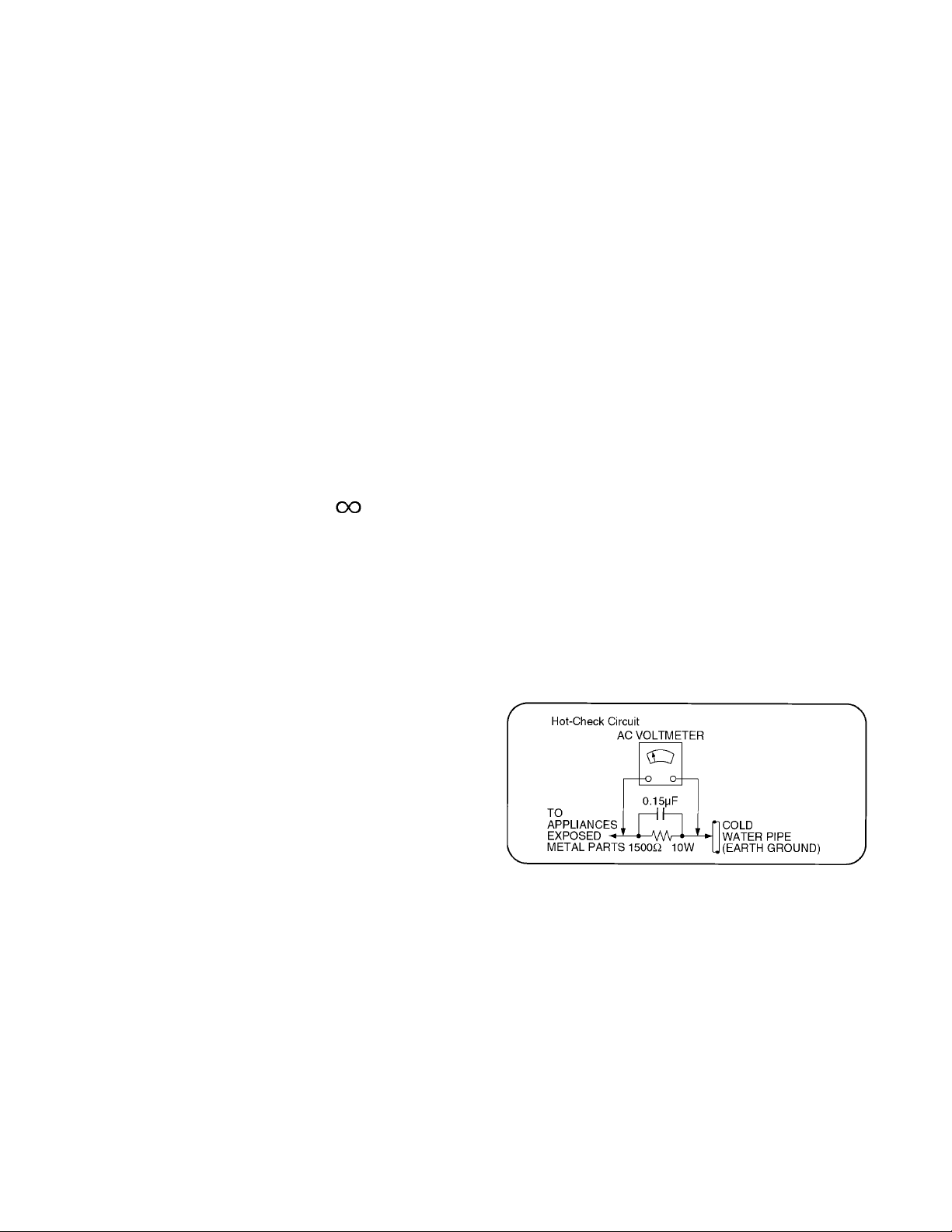
1.1.2. Leakage Current Hot Check (See Figure 1.)
1. Plug the AC cord directly into the AC outlet. Do not use
an isolation transformer for this check.
2. Connect a 1.5kohm, 10 watts resistor, in parallel with a
0.15μF capacitors, between each exposed metallic part
on the set and a good earth ground such as a water pipe,
as shown in Figure 1.
3. Use an AC voltmeter, with 1000 ohms/volt or more sensitivity, to measure the potential across the resistor.
4. Check each exposed metallic part, and measure the voltage at each point.
5. Reverse the AC plug in the AC outlet and repeat each of
the above measurements.
6. The potential at any point should not exceed 0.75 volts
RMS. A leakage current tester (Simpson Model 229 or
equivalent) may be used to make the hot checks, leakage
current must not exceed 1/2 milliamp. In case a measurement is outside of the limits specified, there is a possibility
of a shock hazard, and the equipment should be repaired
and rechecked before it is returned to the customer.
Figure 1
3
Page 4

2 Warning
2.1. Prevention of Electrostatic Discharge (ESD) to Electrostatically Sensitive (ES) Devices
Some semiconductor (solid state) devices can be damaged easily by static electricity. Such components commonly are called Electrostatically Sensitive (ES) Devices. Examples of typical ES devices are integrated circuits and some field-effect transistors and
semiconductor [chip] components. The following techniques should be used to help reduce the incidence of component damage
caused by electrostatic discharge (ESD).
1. Immediately before handling any semiconductor component or semiconductor-equipped assembly, drain off any ESD on your
body by touching a known earth ground. Alternatively, obtain and wear a commercially available discharging ESD wrist strap,
which should be removed for potential shock reasons prior to applying power to the unit under test.
2. After removing an electrical assembly equipped with ES devices, place the assembly on a conductive surface such as aluminum foil, to prevent electrostatic charge buildup or exposure of the assembly.
3. Use only a grounded-tip soldering iron to solder or unsolder ES devices.
4. Use only an anti-static solder removal device. Some solder removal devices not classified as [anti-static (ESD protected)] can
generate electrical charge sufficient to damage ES devices.
5. Do not use freon-propelled chemicals. These can generate electrical charges sufficient to damage ES devices.
6. Do not remove a replacement ES device from its protective package until immediately before you are ready to install it. (Most
replacement ES devices are packaged with leads electrically shorted together by conductive foam, aluminum foil or comparable conductive material).
7. Immediately before removing the protective material from the leads of a replacement ES device, touch the protective material
to the chassis or circuit assembly into which the device will be installed.
Caution
Be sure no power is applied to the chassis or circuit, and observe all other safety precautions.
8. Minimize bodily motions when handling unpackaged replacement ES devices. (Otherwise ham less motion such as the brushing together of your clothes fabric or the lifting of your foot from a carpeted floor can generate static electricity (ESD) sufficient
to damage an ES device).
4
Page 5
2.2. About lead free solder (PbF)
Note: Lead is listed as (Pb) in the periodic table of elements.
In the information below, Pb will refer to Lead solder, and PbF will refer to Lead Free Solder.
The Lead Free Solder used in our manufacturing process and discussed below is (Sn+Ag+Cu).
That is Tin (Sn), Silver (Ag) and Copper (Cu) although other types are available.
This model uses Pb Free solder in it’s manufacture due to environmental conservation issues. For service and repair work, we’d
suggest the use of Pb free solder as well, although Pb solder may be used.
PCBs manufactured using lead free solder will have the PbF within a leaf Symbol PbF stamped on the back of PCB.
Caution
• Pb free solder has a higher melting point than standard solder. Typically the melting point is 50 ~ 70 °F (30~40 °C) higher. Please
use a high temperature soldering iron and set it to 700 ± 20 °F (37 0 ± 10 °C).
• Pb free solder will tend to splash when heated too high (about 1100 °F or 600 °C).
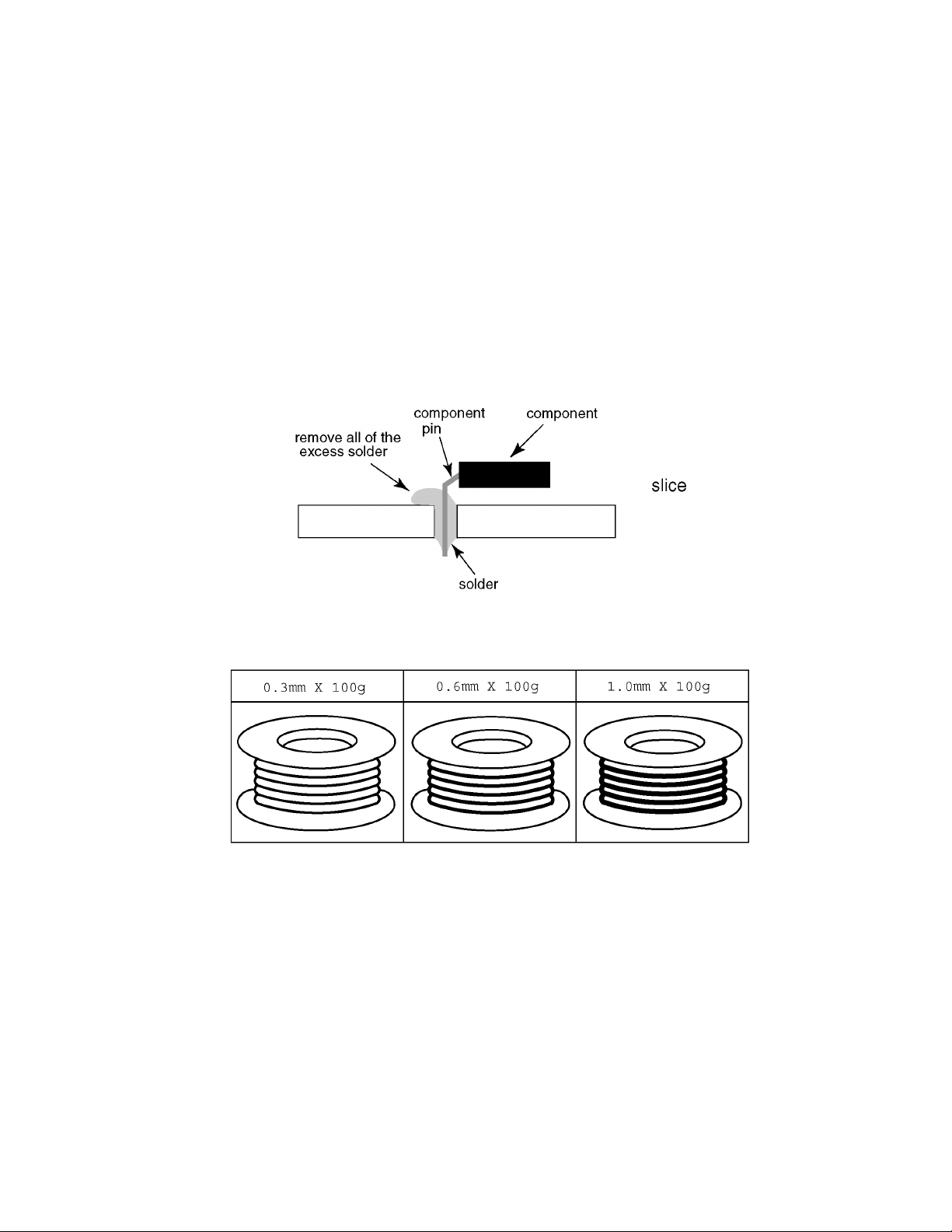
If you must use Pb solder, please completely remove all of the Pb free solder on the pins or solder area before applying Pb solder. If this is not practical, be sure to heat the Pb free solder until it melts, before applying Pb solder.
• After applying PbF solder to double layered boards, please check the component side for excess solder which may flow onto the
opposite side. (see figure below)
Suggested Pb free solder
There are several kinds of Pb free solder available for purchase. This product uses Sn+Ag+Cu (tin, silver, copper) solder. However, Sn+Cu (tin, copper), Sn+Zn+Bi (tin, zinc, bismuth) solder can also be used.
5
Page 6
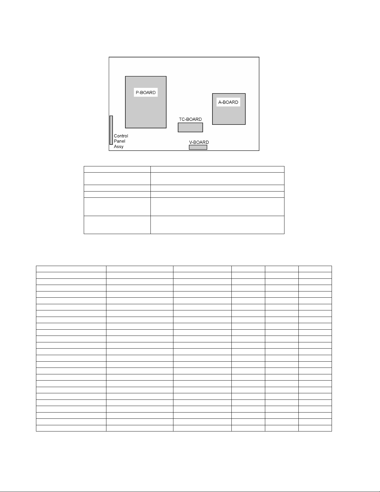
3 Service Navigation
3.1. Service Hint
Board Name Function
A-Board Speaker out, AV Terminal, HDMI in, SD Card, PC in, iPod
V-Board Remote Receiver, LED
TC-Board T-CON
P-Board Power (AC/DC), DC-DC
Control Panel Assy Control Button, Power switch
Digital Signal Processor, Nile-Tcon, Tuner
Non serviceable
P-Board should be exchanged for service.
Non serviceable
Control Panel Assy should be exchanged for service.
3.2. Applicable signals
* Mark: Applicable input signal for Component (Y, PB, PR), HDMI and PC
horizontal frequency (kHz) vertical frequency (Hz) COMPONENT HDMI PC
525 (480) / 60i 15.73 59.94 * *
525 (480) /60p 31.47 59.94 * *
750 (720) /60p 45.00 59.94 * *
1,125 (1,080) /60i 33.75 59.94 * *
1,125 (1,080) /60p 67.43 59.94 *
1,125 (1,080) /60p 67.50 60.00 *
1,125 (1,080) /24p 26.97 23.98 *
1,125 (1,080) /24p 27.00 24.00 *
640 × 400 @70 31.47 70.08 *
640 × 480 @60 31.47 59.94 *
Macintosh13 inch (640 × 480) 35.00 66.67 *
640 × 480 @75 37.50 75.00 *
852 × 480 @60 31.44 59.89 *
800 × 600 @60 37.88 60.32 *
800 × 600 @75 46.88 75.00 *
800 × 600 @85 53.67 85.08 *
Macintosh16 inch (832 × 624) 49.73 74.55 *
1,024 × 768 @60 48.36 60.00 *
1,024 × 768 @70 56.48 70.07 *
1,024 × 768 @75 60.02 75.03 *
1,024 × 768 @85 68.68 85.00 *
Macintosh 21 inch (1,152 ×870) 68.68 75.06 *
1,280 × 768 @60 47.78 59.87 *
1,280 × 1,024 @60 63.98 60.02 *
1,366 × 768 @60 48.39 60.04 *
Note
• Signals other than above may not be displayed properly.
• The above signals are reformatted for optimal viewing on your display.
6
Page 7

4 Specifications
Power Source AC 110-127 V, 60 Hz
Power Consumption
Maximum 137 W
Standby Condition 0.3 W
Display panel
Aspect Ratio 16:9
Visible screen size 42 inch class (42.0 inches measured diagonally)
(W × H × Diagonal) 36.6 inch × 20.6 inch × 42.0 inch (930 mm × 523 mm × 1,067 mm)
(No. of pixels) 2,073,600 (1,920 (W) × 1,080 (H)) [5,760 × 1,080 dots]
Sound
Speaker 1-way 2 speakers slim under SP System
Audio Output 20 W [10 W + 10 W] ( 10 % THD )
PC signals VGA, SVGA, XGA, WXGA, SXGA
Channel CapabilityATSC/NTSC (Digital/Analog)
Operating Conditions Temperature: 32 °F - 95 °F (0 °C - 35°C)
Connection Terminals
VIDEO IN 1-2 VIDEO: RCA PIN Type × 1 1.0 V [p-p] (75 Ω)
COMPONENT IN Y: 1.0 V [p-p] (including synchronization)
HDMI 1-3 TYPE A Connector × 3.
PC D-SUB 15PIN: R,G,B / 0.7 V [p-p] (75 Ω)
Dock for iPod DC 5 V 500 mA MAX
Card slot SD CARD slot × 1
DIGITAL AUDIO OUT PCM / Dolby Digital, Fiber Optic
FEATURES 3D Y/C FILTER, CLOSED CAPTION,
Dimensions (W × H × D)
Including TV stand 40.7 inch × 27.5 inch
TV Set only 40.7 inch × 25.8 inch × 1.5 (3.0) inch (1,032 mm × 655 mm × 39 (77) mm)
Mass
Including TV stand 47.4 lb. (21.5 kg) NET
TV Set only 40.8 lb. (18.5 kg) NET
Horizontal scanning frequency 31 - 69 kHz
Vertical scanning frequency 59 - 86 Hz
VHF/ UHF: 2 - 69, CATV: 1 - 135
Humidity: 20 % - 80 % RH (non-condensing)
AUDIO L - R: RCA PIN Type × 2 0.5 V [rms]
PB, PR: ±0.35 V [p-p]
AUDIO L-R: RCA PIN Type × 2 0.5 V [rms]
O This TV supports [HDAVI Control 5] function.
HD, VD / 1.0 - 5.0 V [p-p] (high impedance)
V-Chip, HDAVI Control 5
Vesa compatible, VIERA IMAGE VIEWER
× 13
.0 inch (1,032 mm × 697
mm × 329 mm)
Note
Design and Specifications are subject to change without notice. Mass and Dimensions shown are approximate.
7
Page 8
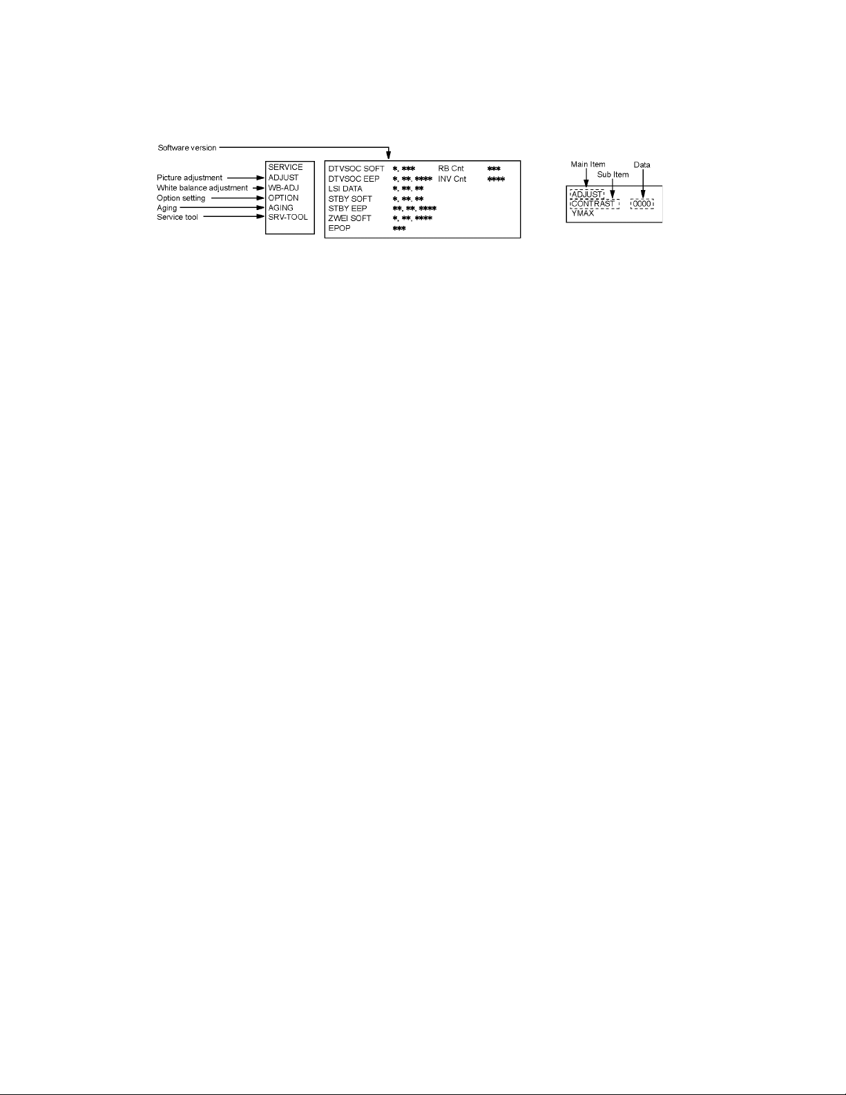
5 Service Mode
5.1. How to enter into Service Mode
While pressing [VOLUME ( - )] button of the main unit, press [INFO] button of the remote control three times within 2 seconds.
5.1.1. Key command
[1] button...Main items Selection in forward direction
[2] button...Main items Selection in reverse direction
[3] button...Sub items Selection in forward direction
[4] button...Sub items Selection in reverse direction
[VOL] button...Value of sub items change in forward direction ( + ), in reverse direction ( - )
8
Page 9
5.1.2. Contents of adjustment mode
• Value is shown as a hexadecimal number.
• Preset value differs depending on models.
• After entering the adjustment mode, take note of the value in each item before starting adjustment.
Main item Sub item Sample Data Remark
ADJUST CONTRAST 01
COLOR 00
TINT 00
SUB-BRT 000
BACKLGT 9FFF
V COM 1B4
WB-ADJ R-GAIN F7
G-GAIN FB
B-GAIN DB
R-CENT 82
G-CENT 80
B-CENT 86
OPTION Boot ROM Factory Preset.
STBY-SET 00
EMERGENCY ON
CLK MODE OFF
CLOCK FC4
EDID-CLK HIGH
AGING COUNT Built-in test patterns can be
ALL WHITE
ALL BLACK
ALL RED
ALL GREEN
ALL_BLUE
RASTER1
RASTER2
RASTER3
RASTER4
4DIN1
4DIN2
GRAY WHITE
GRAY RED
GRAY GREEN
GRAY BLUE
FLICKER0
GS1
1 PIX STRIPE
2 PIX STRIPE
1 LINE_STRIPE
COLORBAR
WIDHT COLORBAR
OUTER
LIGHT CHECK
FLICKER1
FLICKER2
FLICKER3
SRV-TOOL 00 See next.
displayed.
5.1.3. How to exit
Switch off the power with the [POWER] button on the main unit or the [POWER] button on the remote control.
9
Page 10
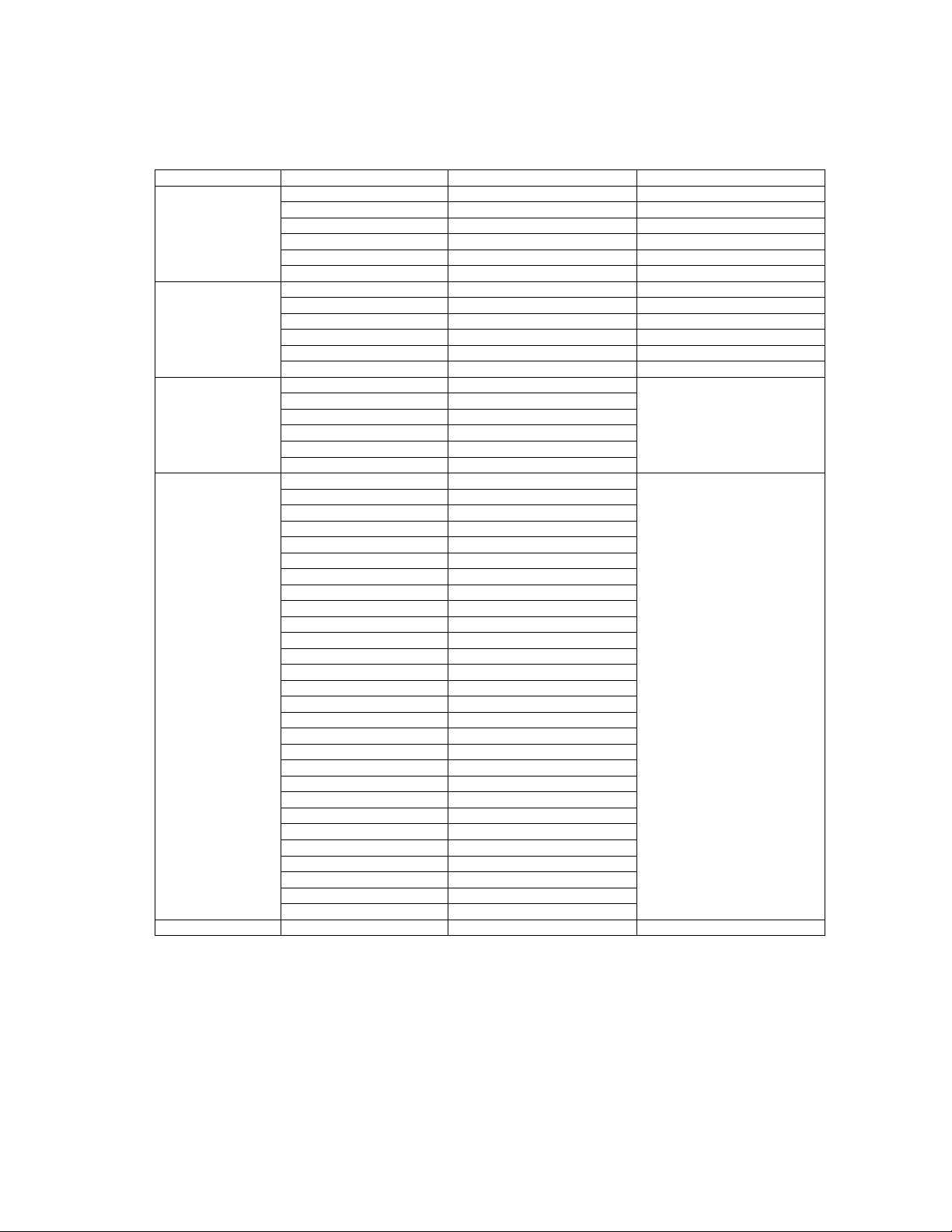
5.2. SRV-TOOL
5.2.1. How to access
1. Select [SRV-TOOL] in Service Mode.
2. Press [OK] button on the remote control.
5.2.2. Display of SOS History
SOS History (Number of LED blinking) indication.
From left side; Last SOS, before Last, three occurrence before, 2nd occurrence after shipment, 1st occurrence after shipment.
This indication except 2nd and 1st occurrence after shipment will be cleared by [Self-check indication and forced to factory shipment setting].
5.2.3. POWER ON TIME/COUNT
Note : To display TIME/COUNT menu, highlight position, then press MUTE for 3sec.
Time : Cumulative power on time, indicated hour : minute by decimal
Count : Number of ON times by decimal
Note : This indication will not be cleared by either of the self-checks or any other command.
5.2.4. Exit
1. Disconnect the AC cord from wall outlet.
10
Page 11
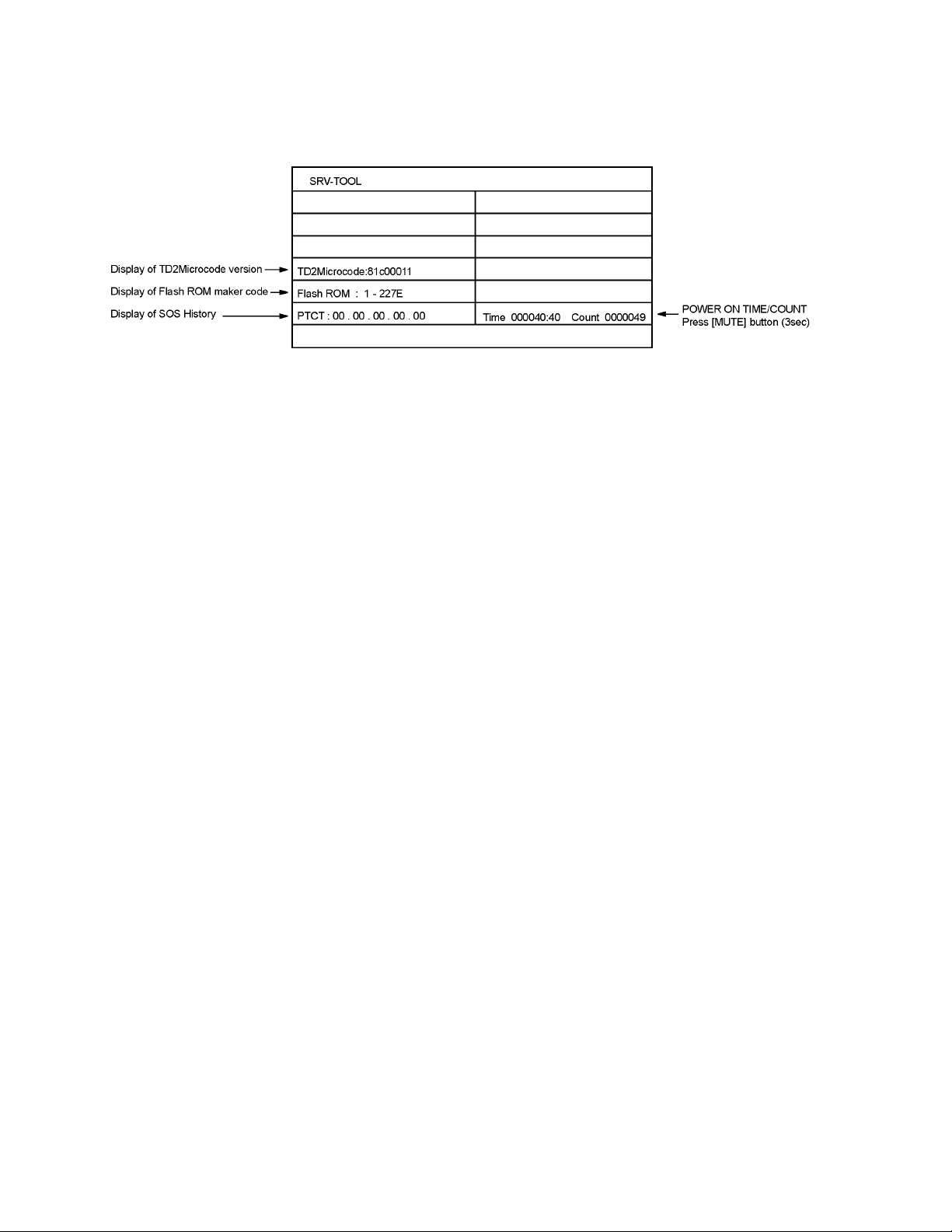
5.3. Hotel mode
1. Purpose
Restrict a function for hotels.
2. Access command to the Hotel mode setup menu
In order to display the Hotel mode setup menu, please
enter the following command (within 2 second).
[TV] : Vol. [Down] + [REMOTE] : INPUT (3 times)
Then, the Hotel mode setup menu is displayed.
3. To exit the Hotel mode setup menu
Disconnect AC power cord from wall outlet.
4. Explain the Hotel mode setup menu
item Function
Mode Select hotel mode off/on
Input Select input signal modes.
Set the input, when each time power is
switched on.
Selection:
-/RF/HDMI1/HDMI2/HDMI3/Component/
Video1/Video2/PC
• OFF: give priority to a last memory.
Channel Select channel when input signal is RF.
Set the channel, each time power is switched
on.
Selection:
Any channel number or [-].
[-] means the channel when turns off.
Volume Adjust the volume when each time powe r is
switched on.
Range:
0 to 100
Vol. Max Adjust maximum volume.
Range:
0 to 100
OSD Ctrl Restrict the OSD.
Selection:
OFF/PATTERN1
• OFF: No restriction
• PATTERN1: restriction
FP Ctrl Selec t front key conditions .
Selection:
OFF/ALL/PATTERN1
• OFF: altogether valid.
• ALL: altogether invalid.
• PATTERN1: only input key is valid.
Pow Ctrl Select POWER-ON/OFF con dition when AC
power cord is disconnected and then connected.
OFF: The same condition when AC power
cord is disconnected.
ON: Forced power ON condition.
11
Page 12
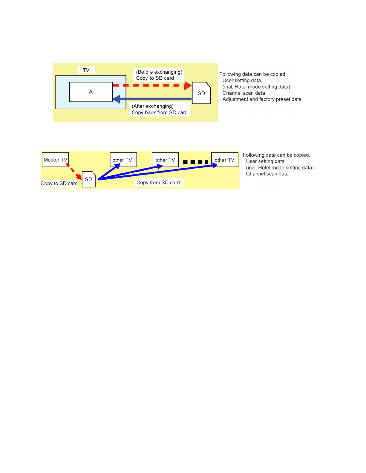
5.4. Data Copy by SD Card
5.4.1. Purpose
(a) Board replacement (Copy the data when exchanging A-board):
When exchanging A-board, the data in original A-board can be copied to SD card and then copy to new A-board.
(b) Hotel (Copy the data when installing a number of units in hotel or any facility):
When installing a number of units in hotel or any facility, the data in master TV can be copied to SD card and then copy to other
TVs.
5.4.2. Preparation
Make pwd file as startup file for (a) or (b) in a empty SD card.
1. Insert a empty SD card to your PC.
2. Right-click a blank area in a SD card window, point to New, and then click text document. A new file is created by default
(New Text Document.txt).
3. Right-click the new text document that you just created and select rename, and then change the name and extension of the
file to the following file name for (a) or (b) and press ENTER.
File name:
(a) For Board replacement : boardreplace.pwd
(b) For Hotel : hotel.pwd
Note:
Please make only one file to prevent the operation error.
No any other file should not be in SD card.
12
Page 13
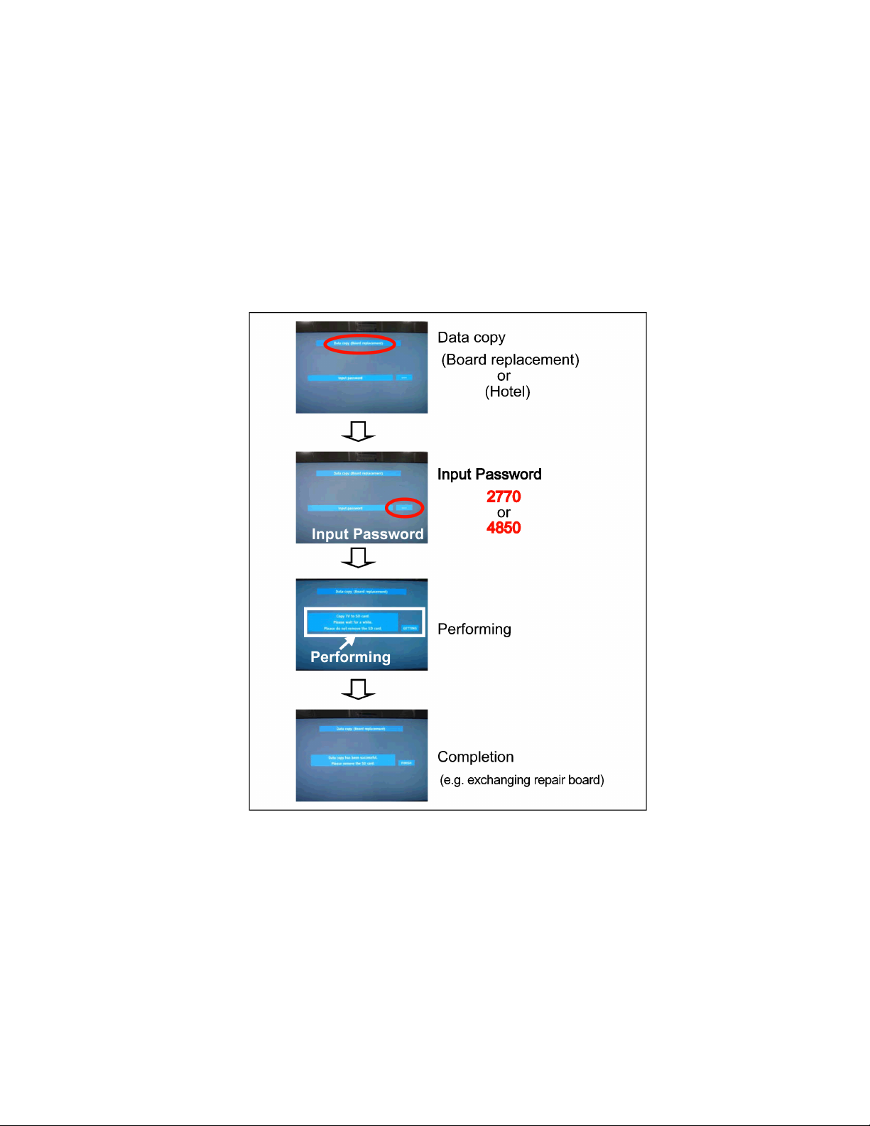
5.4.3. Data copy from TV set to SD Card
1. Turn on the TV set.
2. Insert SD card with a startup file (pwd file) to SD slot.
On-screen Display will be appeared according to the startup file automatically.
3. Input a following password for (a) or (b) by using remote control.
(a) For Board replacement : 2770
(b) For Hotel : 4850
Data will be copied from TV set to SD card.
It takes around 2 to 6 minutes maximum for copying.
4. After the completion of copying to SD card, remove SD card from TV set.
5. Turn off the TV set.
Note:
Following new folder will be created in SD card for data from TV set.
(a) For Board replacement : user_setup
(b) For Hotel : hotel
13
Page 14
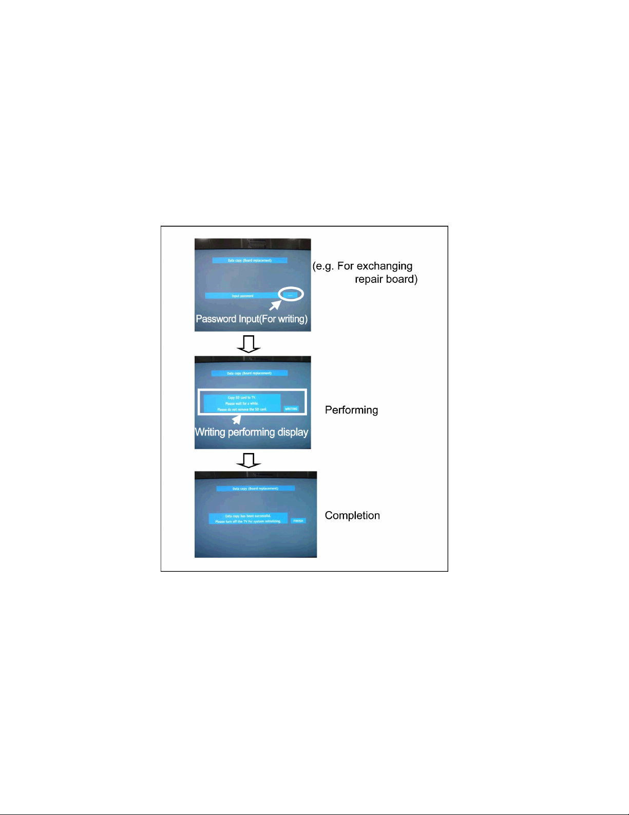
5.4.4. Data copy from to SD Card to TV set
1. Turn on the TV set.
2. Insert SD card with Data to SD slot.
On-screen Display will be appeared according to the Data folder automatically.
3. Input a following password for (a) or (b) by using remote control.
(a) For Board replacement : 2771
(b) For Hotel : 4851
Data will be copied from SD card to TV set.
4. After the completion of copying to SD card, remove SD card from TV set.
(a) For Board replacement : Data will be deleted after copying (Limited one copy).
(b) For Hotel : Data will not be deleted and can be used for other TVs.
5. Turn off the TV set.
Note:
1. Depending on the failure of boards, function of Data copy for board replacement does not work.
2. This function can be effective among the same model numbers.
14
Page 15
6 Troubleshooting Guide
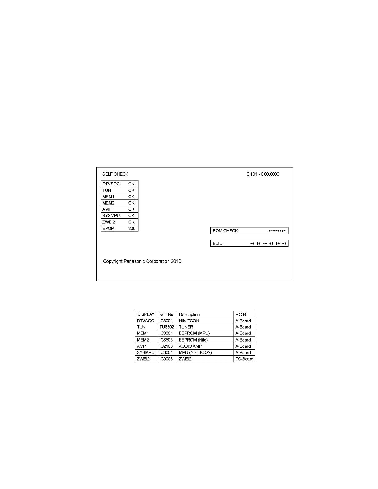
Use the self-check function to test the unit.
1. Checking the IIC bus lines
2. Power LED Blinking timing
6.1. Check of the IIC bus lines
6.1.1. How to access
Self-check indication only:
Produce TV reception screen, and while pressing [VOLUME ( - )] button on the main unit, press [OK] button on the remote control
for more than 3 seconds.
Self-check indication and forced to factory shipment setting:
Produce TV reception screen, and while pressing [VOLUME ( - )] button on the main unit, press [MENU] button on the remote con-
trol for more than 3 seconds.
6.1.2. Exit
Disconnect the AC cord from wall outlet.
6.1.3. Screen display
6.1.4. Check Point
Confirm the following parts if NG was displayed.
15
Page 16
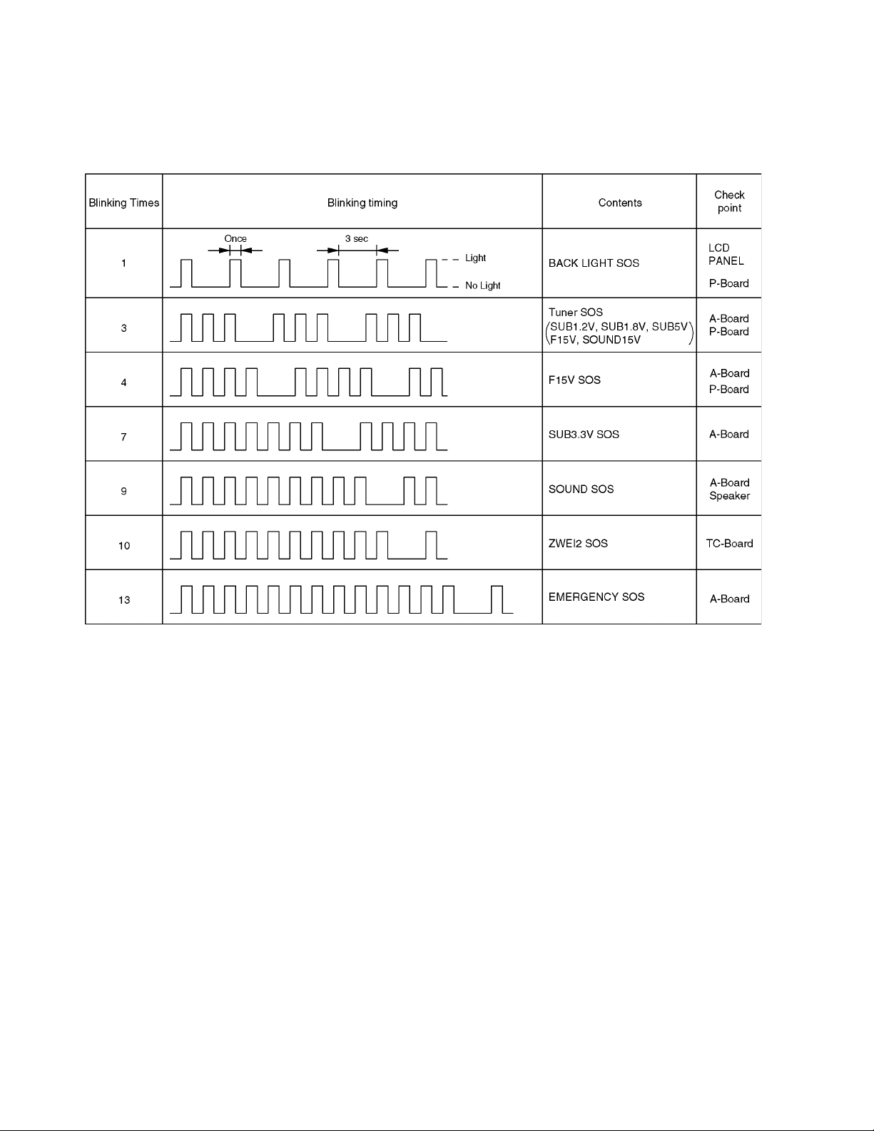
6.2. Power LED Blinking timing chart
1. Subject
Information of LED Flashing timing chart.
2. Contents
When an abnormality has occurred the unit, the protection circuit operates and reset to the stand by mode. At this time, the
defective block can be identified by the number of blinks of the Power LED on the front panel of the unit.
16
Page 17
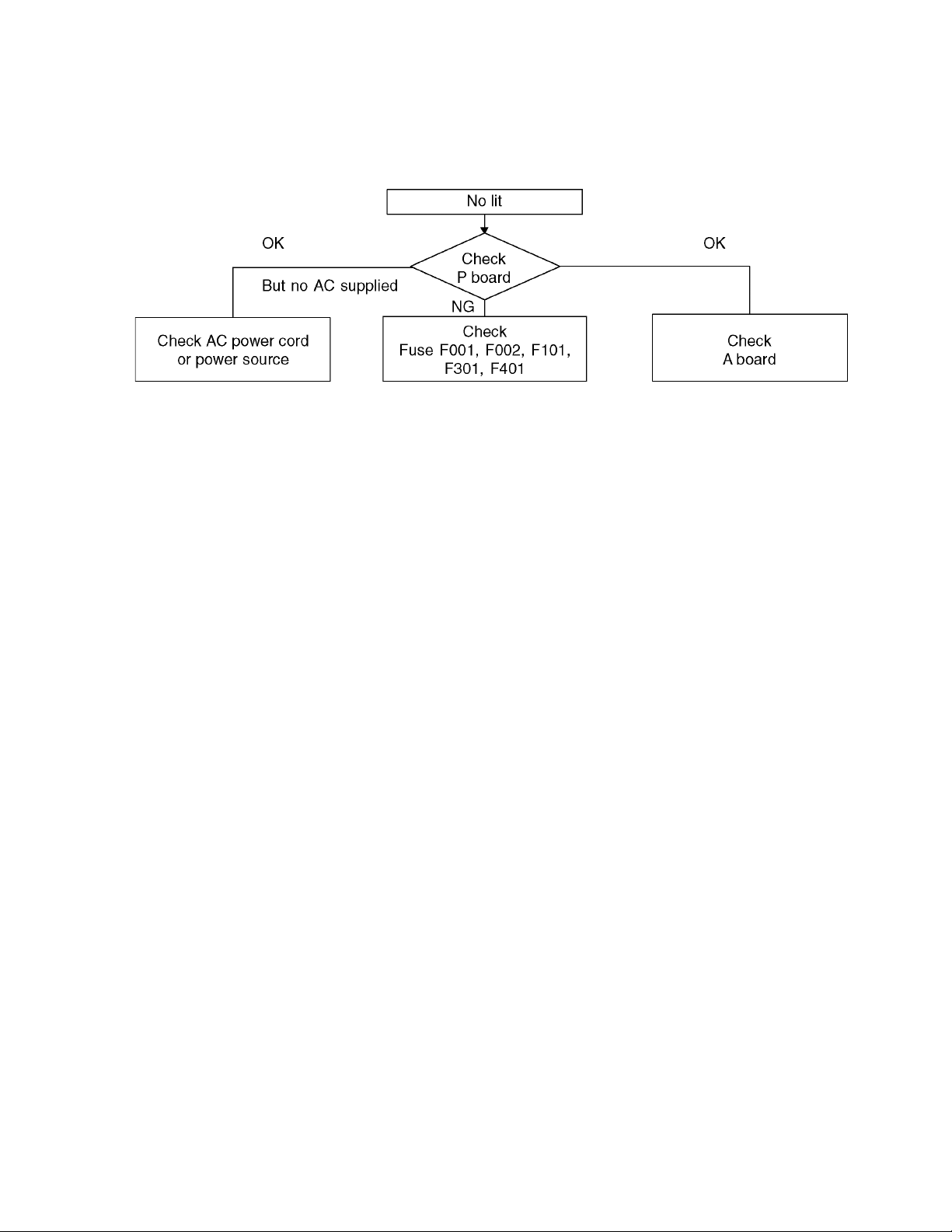
6.3. No Power
First check point
There are following 2 states of No Power indication by power LED.
1. No lit
2. Red is lit then turns red blinking a few seconds later. (See 6.2.)
17
Page 18
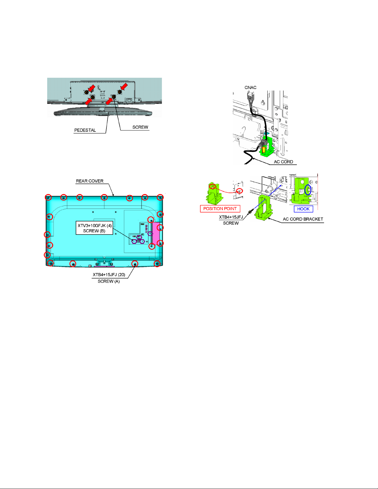
7 Disassembly and Assembly Instructions
7.1. Pedestal
1. Lay down the unit so that the rear cover faces upward.
2. Remove the 4 screws.
3. Remove the pedestal.
7.2. Rear cover
1. Remove the 20 screws (A).
2. Remove the 4 screws (B).
3. Remove the rear cover.
7.3. AC cord
1. Remove the bushing of the AC cord from the AC cord
bracket.
2. Remove the screw and Remove the AC cord bracket.
3. Disconnect the connector (CNAC) of AC cord.
18
Page 19
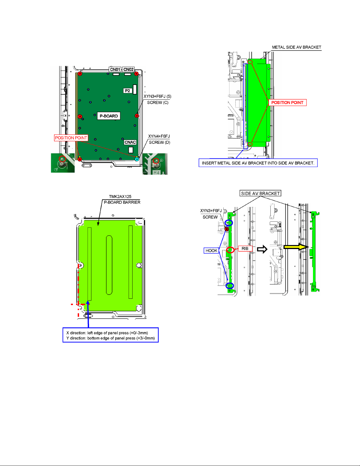
7.4. P-Board
1. Remove the 5 screws (C).
2. Remove the 1 screw (D).
3. Disconnect the connectors (CNAC, CN01, CN02 and P2).
4. Remove the P-Board.
5. Remove the P-Board barrier.
7.5. Side AV bracket
1. Remove the Metal side AV bracket.
2. Remove the 1 screw.
3. Remove the side AV bracket.
19
Page 20
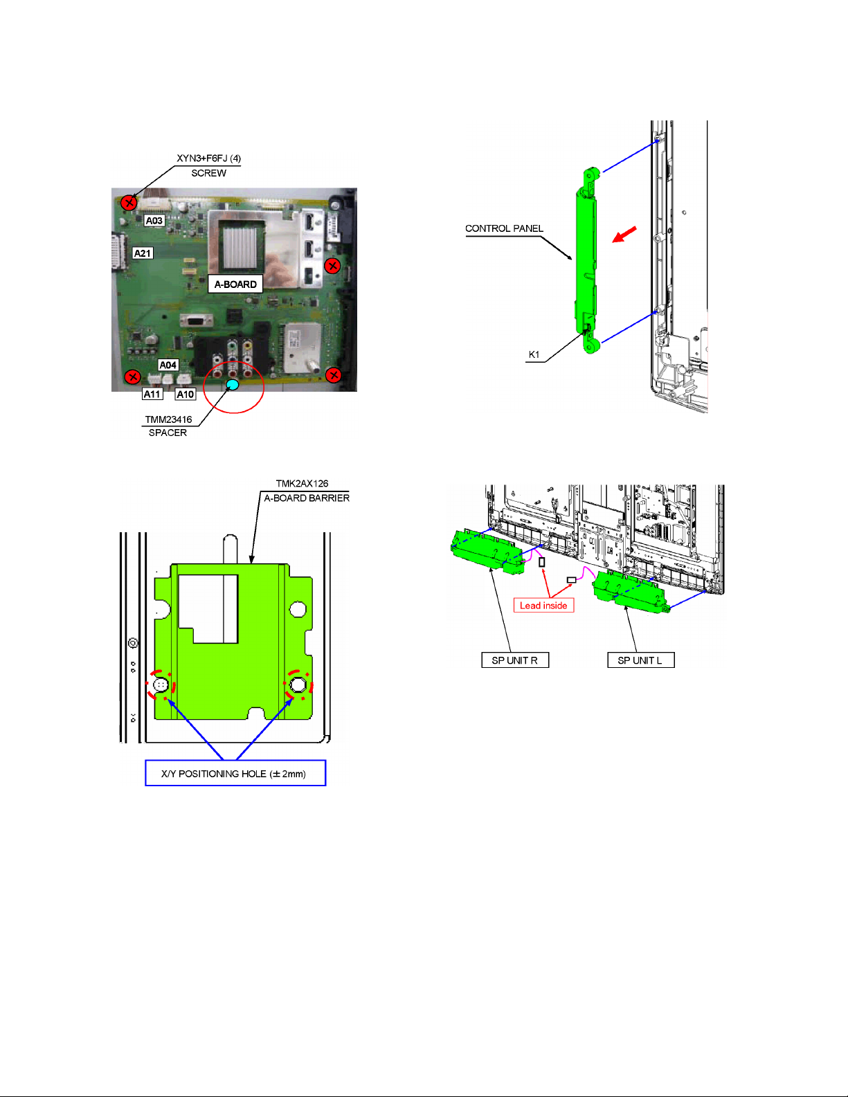
7.6. A-Board
1. Remove the 4 screws.
2. Disconnect the connectors (A03, A04, A10, A11 and
A21).
3. Remove the A-Board.
4. Remove the A-Board barrier.
7.7. Control panel
1. Disconnect the connector (K1).
2. Remove the control panel.
7.8. Speaker
1. Remove the speaker.
20
Page 21
7.9. Metal bracket bottom
1. Remove the 4 screws (E).
2. Remove the 2 screws (F).
3. Remove the Metal bracket bottom.
7.10. TC-Board
1. Remove the 2 screws.
2. Disconnect the connectors (TC01, TC04, TC05 and
TC06).
3. Remove the TC-Board.
4. Remove the T-CON barrier.
21
Page 22
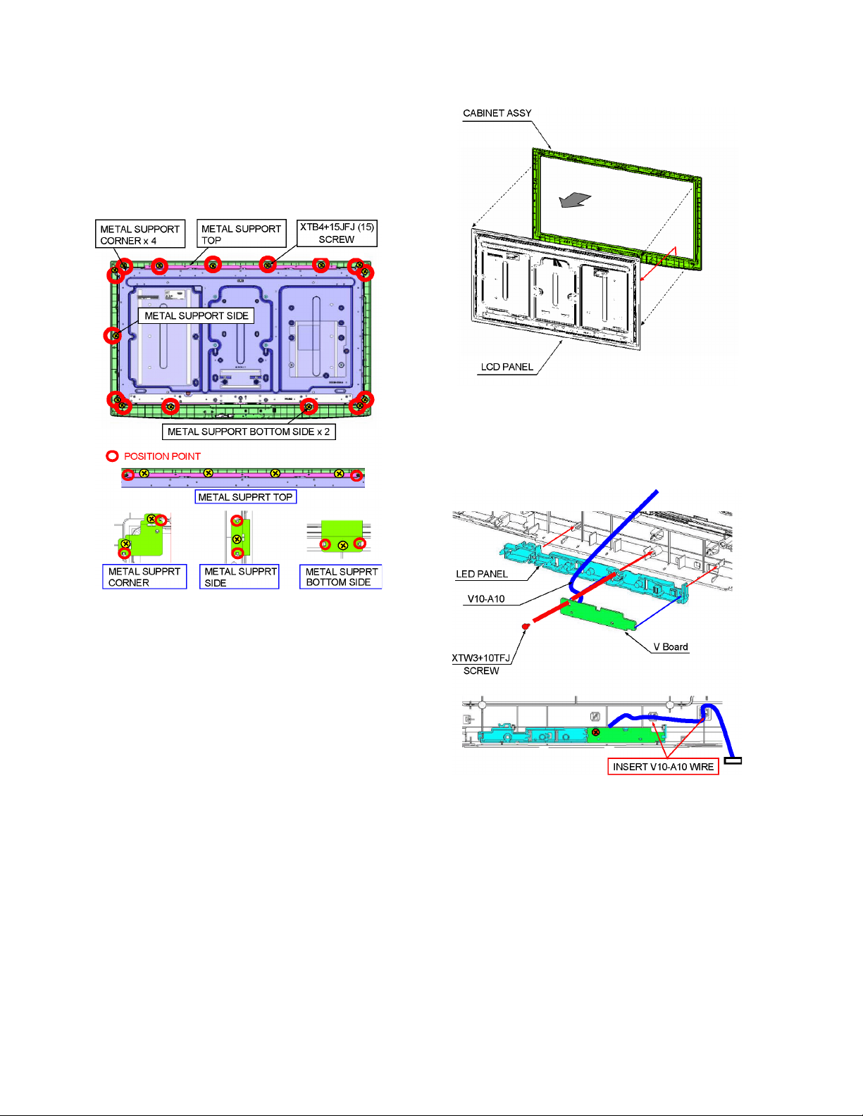
7.11. Metal support
1. Remove the 4 screws.
2. Remove the Metal support top.
3. Remove the 8 screws.
4. Remove the Metal support corner.
5. Remove the 1 screw.
6. Remove the Metal support side.
7. Remove the 2 screws.
8. Remove the Metal support bottom side.
7.12. LCD Panel
1. Remove the LCD panel.
7.13. V-Board
1. Remove the 1 screw.
2. Disconnect the connector (V10).
3. Remove the V-Board.
22
Page 23

7.14. EMI processing
23
Page 24

242526
Page 25

Page 26

Page 27

8 Measurements and Adjustments
8.1. VCOM Adjustment (Flicker Adjustment)
8.1.1. General information:
When replacing LCD panel, TC board (T-CON) or both, [VCOM] Adjustment have to be done.
Data for VCOM Adjustment is different depend on the LCD panel and the data is stored in TC board.
Adjustment procedures are as follows.
8.1.2. Adjustment procedures:
When replacing LCD panel, TC board or both, [VCOM] Adjustment have to be done.
1. Set to Service mode
While pressing [ VOLUME ( - ) ] button of the main unit, press [ INFO ] button of the remote control three times within 2 seconds.
2. Go into VCOM value indication
Go into main item ADJUST by pressing [1] button on remote control.
Go into sub item VCOM by pressing [3] button on remote control.
Adjustment value of VCOM is displayed.
3. Flicker Confirmation
Go to flicker adjustment screen by pressing [5] button on remote control.
Confirm if flicker can be seen.
No flicker --- Exit from Service mode.
Flicker --- Adjustment have to be done.
4. VCOM Adjustment (Flicker Adjustment)
This procedure writes into EEPROM correct data so the panel does not flicker.
Press remote control [+/ -] button to delete or minimize the flicker in flicker adjustment screen.
Press [ OK ] button. Correct data is automatically written into EEPROM (IC9206).
Caution:
The data can be written into EEPROM only 15 times. Don’t press [ OK ] button many time.
If the data can not be written, replace TC board or IC9206 to new one.
5. Exit from Service mode
Switch off the power with the [ POWER ] button on the main unit or the [ POWER ] button on the remote control.
27
Page 28

8.2. Voltage chart of A-board
VOLTAGE TEST POINT SPECIFICATION
STB3.3V TP4716 3.3 ± 0.16 V
SUB5V TP4724 5 ± 0.25 V
PANEL12V TP5413 12 ± 0.6 V
SOUND15V TP2765 18 ± 2 V
5VS TP2768 6.1 ± 0.3 V
SUB6V TP2767 6.1 ± 0.3 V
(Reception state)
8.3. Picture level adjustment (RF)
Instrument Name Remarks
1. REMOTE TRANSMITTER
2. Ex. Signal (Sprit color bar)
Adjustment or Inspection Procedure Remarks
< procedure >
1. Receive the Sprit color bar.
(Screen mode: ZOOM or FULL Picture mode: DYNAMIC AI: OFF AI Picture: OFF)
*BACK LIGHT +30
< Inspection >
1. Enter Service mode, and select MAIN_ADJ PICTURE.
Volume UP/DOWN key makes GAIN displayed under PICTURE to set.
Pushing the remote controller [OK] key for about 3 seconds, GAIN is suited
to the adjustment value automatically.
(The Sprit Color Bar Pattern)
28
Page 29

(LED:7TIMES)
(LED:1TIMES)
(LED:3TIMES)
**
V
NEUTRAL
STB+3.3V
TMDS DATA
TUNER
STB5V
ANALOG-ASIC
OPTICAL OUT
REMOTE RECEIVER
SUB_ON
A
SUB 3.3V SENSE
C.A.T.S. SENSOR
F15V
174V
V
SOS
A10
SUB5V
SPEAKER(R)
KEYSCAN3
SUB1.8V
RECEIVER
MPU
V
LINE
FILTER
SPEAKER(L)
DCDC
RECTIFIER
SD CARD DATA
FRONT END
SUB1.8V
AV SW
DCDC
SUB1.2V
ERROR DET
SUB1.2V
LVDS DATA_ODD/EVEN
SOS
SUB1.8V DET
A21
L/R
SUB5V DET
C.A.T.S. SENSOR
AMP
18V
BACK LIGHT
POWER
CONTROL
CURCUIT
EEPROM
V
STB3.3V
EEPROM
POWER LED
DCDC
PFC
CONTROL
SD CARD DATA
RELAY_5V
OPTICAL AUDIO OUT
CONTROL
PANEL ASSY
PROCESSOR
Nile-TCON
HDMI I/F
REMOTE RECEIVER
VIDEO2
SIF_OUT
L
SUB3.3V
IFD_OUT
SUB3.3V
TMDS DATA
PNL12V
L/R
OUT
POWER
CONTROL
POWER LED
CNAC
TMDS DATA
STB5V
STB+3.3V
COMP1
R
SUB5V
STANDBY
VOLTAGE
RECTIFIER
PROCESS
VOLTAGE
RECTIFIER
Y/PB/PR
V
TCON
TC
POWER LED(R)
SUB1.2V DET
P2
RECTIFIER
CPU BUS
I/F
CPU BUS
L/R
NOR
FLASH
IPOD
DDR2
SOUND15V
F15V
VOLTAGE
STB5V
DROP
F15V
C.A.T.S. SENSOR
HDMI2
A04
SOUND15V
OPTICAL
PNL12V
K1
AG_SOS
PC
A11
REMOTE IN
L/R
HDMI1
SUB_ON
SD0
VIDEO1
STB5V
KEYSCAN1
(SIDE)
SD
V10
DCDC
LVDS DATA
(SIDE)
A03
F15V
HDMI3
SD CARD
DIGITAL SIGNAL PROCESSOR
SUB5V
LVDS DATA
R/G/B/H/V
AUDIO
SLOT
AUDIO
LIVE
AC CORD
IIC2
MCU_IIC2
STB1.2V
DCDC
PNL12V
STB_RST
MCU_RST
SW_RST
STB+3.3V
SUB+5V SUB+5V
PWM
GMA
TCON
VDD1_3.3V
GCLK
LVDD16V
DCDC
ZW1.2V
TC01
ZW1.2V
EEPROM
LVCC3.3V
VDD1_3.3V
LVCC3.3V
LEVEL SHIFTER
LVDD16V
TC05
ZWEI2
LVDD16V
LVCC3.3V
PNL12V
mini_LVDS_
LEFT
TC04
LVCORE1.2V
H_VDD8V
DCDC
H_VDD8V
PANEL
mini_
LVDS
CLK
BACK LIGHT
FLASH
LVCORE1.2V
CONTROL
mini_LVDS_
RIGHT
TC06
VDD
DCDC
rDAC
LVDS
BUCK_CONV
VGI_N/P
H_VDD8V
LCD PANEL
PANEL
PWM
CN01,CN02
ARC
SUB3.3V
BACK LIGHT SOS
BACK LIGHT ON
BACK LIGHT SOS
BACK LIGHT ON
(LED:7TIMES)
(LED:1TIMES)
(LED:3TIMES)
POWER SUPPLY
P
9 Block Diagram
9.1. Main Block Diagram
29
Page 30

9.2. Block (1/3) Diagram
HOT COLD
(LED:3TIMES)
POWER LED
V
REMOTE RECEIVER
C.A.T.S. SENSOR
SN2500
C.A.T.S.
SENSOR
RM2500
REMOTE
RECEIVER
D2500A
POWER LED
+3.3V
DIGITAL SIGNAL PROCESSOR
A
R_LED_ON
C.A.T.S.
REMOTE IN
SUB+5V
STB+3.3V
A10
POWER LED(R)
7
4
3
1
5
C.A.T.S.
REMOTE IN
SUB5V
STB3.3V
V10
1
4
5
7
+5V
3
RECTIFIER
L003
L001
F001
4A
AC250V
CNAC
AC CORD
BACK
LIGHT
ON
PWM
SOS Latch
SOS
Q355
PWM
POWER SUPPLY
P
D102
LINE
FILTER
1
2
12V
Q356
L202
F002
4A
AC250V
Q357
D201
Q201
Q202
Q203
CONTROL
D205
I201
PFC
D105-D108
RECTIFIER
CURRENT
CONTROL/DRIVER
VCC
PWM
SENSE
I351A
Q351A
SOS
CURRENT
CONTROL/DRIVER
VCC
PWM
SENSE
I351B
Q351B
SOS
Q204
D
G
D
G
D210,D211
F101
2A AC250V
D409
D403
STB
CONTROL
I401
Q401
AC IN
DET
SUB_ON
Q305
Q352A
CONTROL
Q352B
CONTROL
4A AC250V
F301
Q501
I501
V_DET
R003
F401
D402
PHOTO COUPLER
PHOTO COUPLER
PHOTO COUPLER
PHOTO COUPLER
Q301,Q302
RESONANCE
I301
POWER
CONTROL
L401
I402
PHOTO COUPLER
I451
PHOTO COUPLER
I453
PHOTO COUPLER
I352A
I353A
I352B
I353B
S102
S101
S103
T401
L352A
L353A
D3A1-D3F1
L352B
L353B
D3G1-D3L1
D451
STB6V
OVP
OVP
HOT COLD
T301
I551
PHOTO COUPLER
I751
PHOTO COUPLER
12V ERROR DET
D452
SUB_ON
Q452
15V
+
D3A2-D3C2/D3D2-D3F2
I3A1-I3C1/I3D1-I3F1
V IN V OUT
LED DRIVER
D3G2-D3I2/D3J2-D3L2
I3G1-I3I1/I3J1-I3L1
V IN V OUT
LED DRIVER
D353
D363
D653
I752
Q556
L451
I452
STB5.8V
ERROR DET
D753
D755
SUB_ON
++ +
D554
174V
18V
15V
D565
L651
SOS Latch
OVP DET
I354A
OVP DET
I354B
Q553
D357A
D357B
D564
SOS
D566
STB6V_ON
D560
D557
D559
D556
D558
D555
Q554
+
+
-
V+
I552
AC IN_ON
174V
ERROR DET
174V
ERROR DET
CONTROL PANEL ASSY
174V
Q551
SOS
D553
I553
ERROR
DET
Q454
Q453
Q354A
D358A
Q354B
D358B
OPERATION KEYS
POWER SW
15V
L751
BACK LIGHT
SOS
Q555
SOS_ON
RELAY_ON
SUB_ON
STB6V
BACK
LIGHT ON
PWM
#1 Anode
#1
Cathode
#2
Cathode
#2 Anode
#3 Anode
#3
Cathode
#4
Cathode
#4 Anode
174V
CN01
CN02
K1
P2
7
4
5
12
11
9
1
2
13
15
1
3
4
5
8
9
10
12
1
3
4
5
9
10
11
13
KEYSCAN1
KEYSCAN3
SOUND15V
F15V
F15V
BACK LIGHT
SOS
RELAY
TV_SUB_ON
STB5V
SUB6V
TC06
TO
LED
BACK LIGHT
CIRCUIT
A04
A03
2
4
7
9
10
2
3
5
13
12
1
BACK LIGHT SOS
Q4770
TV_SUB_ON
SUB6V
BACK LIGHT ON
Q2760
Q2761
KEYSCAN1
KEYSCAN3
PANEL_
VCC_ON
SOUND15V
F15V
D5629
Q5613
F15V DET
STB5V
D5600
F15V
DCDC_EN
STB5V
Q5602
IC5608
IC5610
Q5612
ON/OFF
VOLTAGE
DROP
ERROR DET
SUB5V
+5V
SUB1.8V
+1.8V
IC5606
Q5616
SUB1.2V
+1.2V
Q5615
SUB5V
STB5V
SUB1.2V
SUB5V
OVP
IC5605
3.3V
PA4202
AG_SOS
SOS
(LED:3TIMES)
SUB5V
SUB3.3V
SUB1.8V
IC4700
ANALOG-ASIC
STB
+3.3V
STB
+1.2V
STB_RST
SOS_RSV
SOS7
SOS
PANEL_
VCC_ON
ON/OFF
PNL12V
Q5412
SOS8
SOS6
TC05
STB3.3V
STB1.2V
MCU_RESET
SUB1.2V DET
SUB1.8V DET
SUB5V DET
A21
1
5
46
47
49
13
24
29
40
D5604
Q4702
PNL12V
PWM_POWER_ON
LVDS DATA
LVDS DATA
IIC1
D5605
Q4704
IC5601
RESET
D5603
[R(A-D)_0+/-)]
[R(A-D)_E+/-)]
Q4703
MCU_RESET
KEYSCAN3
LVDS DATA
1
2
3
4
5
6
7
8
9
10
11
30
Page 31

9.3. Block (2/3) Diagram
(LED:1TIMES)
(LED:7TIMES)
(LED:3TIMES)
JK2108A
PC_V
Q3208
5V DET
PC_H
10
1
2
3
4
5
6
7
8
9
SOUND15V
STB5V
F15V
i-Pod_V
IIC0_TU
A01
i-Pod
i-Pod_L
i-Pod_R
IC3201
IC3202
AMP
+5V
IC3200
i-Pod
AUTHENTICATION
LSI
PC
PC_R
PC_G
PC_B
JK2102
VIDEO2
(SIDE)
V2_R
V2_L
UATXD1/UARXD1
IPOD_SOS
IPOD_POW_ON
SUB1.2V
V2_V
D1_R
COMP1
D1_L
STB1.2V
JK2101
D1_PB
D1_PR
D1_Y
STB3.3V
VIDEO1
V1_R
V1_L
V1_V
ANT IN
SUB5V
SUB3.3V
SUB1.8V
TV_V
VIDEO
TU8302
TUNER
5V
SUB5V
TUNER
P
VJ5500
SPEAKER_R
IC2106
DIGITAL AUDIO
REMOTE IN
C.A.T.S. SENSOR
POWER LED(R)_ON
SPEAKER_L
A11
2
1
L(-)
L(+)
L_OUT
SPEAKER
3.3V
15V
KEYSCAN1
KEY3/STBY_LED_ON
Q5605
SDIN
SD
4
3
R(+)
R(-)
R_OUT
SPEAKER
IIC1
LVDS_OUT
SUB 3.3V SENSE
(LED:7TIMES)
UATXD1
UARXD1
MCU_
IIC
A17
FOR
A18
A19
SBO0
SBI0
FACTORY
USE
FOR
FACTORY
USE
FOR
FACTORY
USE
IIC0_TU
IIC1
IIC2
MCU_IIC
LVDS DATA
SBO0
SBI0
IIC0
IIC0
IIC1
IIC1
IIC2
IIC2
SUB3.3V
Q4515
TV SUB ON
OPTICAL
ARC_OFF
D2142
AUDIO
OUT
OPTICAL AUDIO OUT
(LED:3TIMES)
MCU_RESET
SOS
AUDIO AMP
SUB3.3V
SOUND15V
SPDIF
DDC 5V_C
IIC_DDC_C
HDMI_CEC
JK4501
HDMI IN 2
TMDS DATA
/CLOCK_B
JK4502
HDMI IN 1
IIC0_TU
IFD_OUT2
IFD_OUT1
IIC0
SIF_OUT
IF_AGC
AFT
AFT
ARC
TMDS DATA/CLOCK_C
DDC 5V_B
IIC_DDC_B
HDMI_CEC
JK4500
HDMI IN 3
(SIDE)
TMDS DATA
/CLOCK_A
DDC 5V_A
IIC_DDC_A
HDMI_CEC
Q8005
HDMI_CEC
SD DATA:4bit
SUB5V
JK8502
SD CARD
SUB3.3V_SD
3.3V
IC5613
IC5607
3.3V
IC5609
3.3V
VINP_VSB
VINN_VSB
SIF
AGC
RF_AFT
IC2110
INVERTER
VSB_I/F
SIF_IN
AGC
AFT
i-Pod
V
L/R
TV
V
VIDEO1
V
L/R
VIDEO2
V
L/R
COMP1
Y/PB/PR
L/R
PC
R/G/B
H/V
SUB3.3V_A
FRONT END
PROCESSOR
AV SW
DDR I/F
RXC
SUB3.3V_HDMI
CPU BUS
I/F
IC8850
RXA
RXB
IIC_DDC_C
IIC_DDC_B
HDMI I/F RECEIVER
LVDS3.3V
3.3V
IIC_DDC_A
STB1.2V
STB3.3V
DDC5V_B
DDC5V_C
VCC
SUB3.3V
DDC5V_A
SUB1.8V
HDMI_CEC_
IN_OUT
IC8001
Nile-TCON
SUB1.2V
CLK
X IN
X8000
25MHZ
X OUT
SD CARD
I/F
MPU
UATXD1/UARXD1
BACK LIGHT SOS
BACK LIGHT ON
(LED:1TIMES)
PWM_POWER_ON
IPOD_POW_ON
IPOD_SOS
PANEL_STB_ON/VCC_ON
IC8002
STB3.3V
MCU_
RESET
DDR2 #0
IC8502
128Mbit
NOR FLASH
IC8503
EEPROM
ED0-ED15
EA1-EA24
IIC2
PWM_POWER_ON
UATXD1/UARXD1
SBO0/SBI0
BACK LIGHT ON
BACK LIGHT SOS
IPOD_SOS
IPOD_POW_ON
TV SUB ON
PANEL_STB_ON/VCC_ON
MCU_
IIC
MCU_RESET
SOS
IC8004
EEPROM
REMOTE IN
C.A.T.S.
POWER LED(R)_ON
KEYSCAN1
SUB3.3V
STB3.3V
KEYSCAN3
DIGITAL SIGNAL PROCESSOR
A
LVDS DATA
11
[R(A-D)_0+/-),R(A-D)_E+/-)]
31
Page 32

9.4. Block (3/3) Diagram
15pin
PWM_POW_ON
LVDS DATA
LVDS DATA
PNL12V
PNL12V
FOR
FACTORY
USE
FOR
FACTORY
USE
CN01
#1 Anode
1
3
4
5
8
9
10
12
P-BOARD
TC
TCON
P2
TC06
Q9001
3
PMW
A21
TC05
3
LVDS_ODD
41
Z_RXAN1/P1-Z_RXDN1/P1
28
LVDS_EVEN
25
Z_RXAN0/P0-Z_RXDN0/P0
12
6
IIC1
5
51
47
TC07
TC08
Z_IIC
PNL12V
PA9001
SI/SO
L_IIC
CN02
1
3
4
5
9
10
11
13
Q9003
+1.2V
+3.3V
IC9004
ZW1.2V
VDD1_3.3V
#2 Anode
#3 Anode
#4 Anode
174V
#1
Cathode
#2
Cathode
174V
174V
#3
Cathode
#4
Cathode
IC9006
ZWEI2
PWMA
OENB
RXDN1/P1
RXAN1/P1
RXDN0/P0
RXAN0/P0
IC9005
RESET
ZW1.2V
VDD1_3.3V
ZW3.3V
IC9205
BACK_CONVERTER
SW
VIN
FB
NRST
IC9003
SPI
FLASH
+1.2V
X9001
+3.3V
XI
R1AM/P
R1DM/P
R4AM/P
R4DM/P
+3.3V
H_VDD8V
XO
SI/SO
PNL12V
mini_LVDS
IC9202
32Kbit
EEPROM
D9205
L_IIC
IC9207
VIN
LED
BACK LIGHT
CIRCUIT
Q9202
LVDD16V
DCDC
SW
FB
CTRLP
FBP
SWB
FBB
FBN
CTRLN
IC9201
TCON
R1AM/P
R1DM/P
R4AM/P
R4DM/P
IIC
3.3V
1.2V
IC9203
LVCORE1.2V
+1.2V
LVDD16V
Q9201
VGL_
CONTROL
PANEL
LCD PANEL
X9201
XI
RLV0+/-
RLV6+/-
LLV0+/-
LLV6+/-
GCLK1-6
VDD_ODD
VDD_EVEN
Q9203
VDD_
CONTROL
VGH
(25-30V)
XO
D9202
CONTROL
LVCC3.3V
PANEL
VGL(-10V)
Z_IIC
mini_LVDS_RIGHT
mini_LVDS_LEFT
IC9204
LEVEL SHIFTER
IN1-6
IN9
IN8
VGH2
VGH1
+V
IC9208
VCOM BOOST
OUT1-6
+
+
-
IC9206
IIC
VCOM
OUT9
OUT8
VGL
OUT
OUT
rDAC
OUT
Q9204
VSD
VS
CLK1-6
VDD_ODD
VDD_EVEN
Q9205
LVCC3.3V
H_VDD8V
LVDD16V
GMA3,4,6,7,
12,13,15,16
RMLV0N/P-RMLV5N/P
LVCC3.3V
H_VDD8V
LVDD16V
VCOMRFB
VCOMR
VDD_EVEN
VDD_ODD
VDD_ODD
VDD_EVEN
VCOMLFB
VCOML
LVDD16V
H_VDD8V
LVCC3.3V
LMLV0N/P-LMLV5N/P
GMA3,4,6,7,
12,13,15,16
VGI_P
VGI_N
CLK1-6
CLK1-6
VGI_N
VGI_P
TC01
TC04
59
48
40
27
25
24
22
21
20
19
17
16
12
11
10
9
8
3
58
53
52
51
50
49
45
44
42
41
40
39
37
36
34
21
13
2
TO
PANEL
CONTROL
FOR RIGHT
TO
PANEL
CONTROL
FOR LEFT
32
Page 33

10 Wiring Connection Diagram
10.1. Caution statement.
Caution:
Please confirm that all flexible cables are assembled correctly.
Also make sure that they are locked in the connectors.
Verify by giving the flexible cables a very slight pull.
10.2. Wiring (1)
33
Page 34

10.3. Wiring (2)
34
Page 35

11 Schematic Diagram
11.1. Schematic Diagram Notes
35
Page 36

11.2. A-Board (1/13) Schematic Diagram
C8001
6.3V
1u
IC8001 A8 P2CKIN
R8058
220
IC8001 E10 P2FIL
IC8001 D11 BIASDA2
C8002
6.3V
1u
IC8001 A9 P3CKIN
IC8001 D12 P3FIL
IC8001 E11 BIASDA3
IC8001 D21 HDMITEST3
IC8001 T22 TEST
IC8001 U22 RIEXT_A
IC8001 D14 AADVCML
IC8001
C1AB00003249
Nile-TCON
TO 9/13
TO 5/13
VSB_INP
VSB_INN
EBUS
DVSS/AVSS
JTAG
TO 3/13
EBADD23/NABSY_N
EBADD22/NAALE
EBADD21/NACLE
EBDAT15
EBDAT14
EBDAT13
EBDAT12
EBDAT11
EBDAT10
EBDAT9
EBDAT8
EBDAT7
EBDAT6
EBDAT5
EBDAT4
EBDAT3
EBDAT2
EBDAT1
EBDAT0
EBADD24
EBADD20
EBADD19
EBADD18
EBADD17
EBADD16
EBADD15
EBADD14
EBADD13
EBADD12
EBADD11
EBADD10
EBADD9
EBADD8
EBADD7
EBADD6
EBADD5
EBADD4
EBADD3
EBADD2
EBADD1
XECS0
XERE
XEWE0
IC8001 A1 VSS
IC8001 A2 VSS
IC8001 B1 VSS
IC8001 B2 VSS
IC8001 P10 VSS
IC8001 P11 VSS
IC8001 P12 VSS
IC8001 P13 VSS
IC8001 P14 VSS
IC8001 P15 VSS
IC8001 P16 VSS
IC8001 P17 VSS
IC8001 P24 VSS
IC8001 R10 VSS
IC8001 R11 VSS
IC8001 R12 VSS
IC8001 R13 VSS
IC8001 R14 VSS
IC8001 R15 VSS
IC8001 R16 VSS
IC8001 R17 VSS
IC8001 R24 VSS
IC8001 T10 VSS
IC8001 T11 VSS
IC8001 T12 VSS
IC8001 T13 VSS
IC8001 T14 VSS
IC8001 T15 VSS
IC8001 T16 VSS
IC8001 T17 VSS
IC8001 U10 VSS
IC8001 U11 VSS
IC8001 U13 VSS
IC8001 U15 VSS
IC8001 U17 VSS
IC8001 AB9 VSS
IC8001 AB12 VSS
IC8001 AB16 VSS
IC8001 AB22 VSS
IC8001 A19 AVSS
IC8001 A26 AVSS
IC8001 A10 AVSS
IC8001 B10 AVSS
IC8001 B19 AVSS
IC8001 B26 AVSS
IC8001 D10 AVSS
IC8001 D15 AVSS
IC8001 AE24 DBGTDO
IC8001 AF24 DBGTCK
IC8001 AD24 DBGTDI
IC8001 Y21 DBGTMS
IC8001 W21 DBGTRST_N
IC8001 AB2 EBDAT15
IC8001 AB1 EBDAT14
IC8001 AC4 EBDAT13
IC8001 AC3 EBDAT12
IC8001 AC2 EBDAT11
IC8001 AC1 EBDAT10
IC8001 AD3 EBDAT9
IC8001 AD2 EBDAT8
IC8001 AD1 EBDAT7
IC8001 AE2 EBDAT6
IC8001 AE1 EBDAT5
IC8001 AE3 EBDAT4
IC8001 AF3 EBDAT3
IC8001 AD4 EBDAT2
IC8001 AE4 EBDAT1
IC8001 AF4 EBDAT0
IC8001 R2 EBCE3_N
IC8001 R1 EBCE2_N
IC8001 T3 DCIN2
IC8001 T2 EBCE5_N
IC8001 T1 EBCE4_N
IC8001 U3 DCIN3
IC8001 U2 EBACK_N
IC8001 U1 SPI_CLK
IC8001 V4 EBBE0_N
IC8001 V3 EBALE_N
IC8001 W4 EBBE1_N
IC8001 W3 NABSY_N
IC8001 W2 EBADD12
IC8001 W1 EBADD11
IC8001 Y4 EBADD10
IC8001 Y3 EBADD9
IC8001
IC8001 Y1 EBADD7
IC8001 AA4 EBADD6
IC8001 AA3 EBADD5
IC8001 AA2 EBADD4
IC8001 AA1 EBADD3
IC8001 AB4 EBADD2
IC8001 AB3 EBADD1
IC8001 P4 ICERST_N
IC8001 P1 EBCE0_N
IC8001 V1 EBOE_N
IC8001 V2 EBWE_N
IC8001 P2 EBCE1_N
IC8001 AC19 VSS
IC8001 AD9 VSS
IC8001 AD18 VSS
IC8001 AE19 VSS
IC8001 AE13 VSS
IC8001 AE15 VSS
IC8001 AE22 VSS
IC8001 AF1 VSS
IC8001 AF2 VSS
IC8001 AF18 VSS
IC8001 K10 VSS
IC8001 L1 VSS
IC8001 L2 VSS
IC8001 L10 VSS
IC8001 L11 VSS
IC8001 L12 VSS
IC8001
IC8001 L14 VSS
IC8001 L15 VSS
IC8001 L16 VSS
IC8001 L17 VSS
IC8001 M10 VSS
IC8001 M11 VSS
IC8001 M12 VSS
IC8001 M13 VSS
IC8001 M14 VSS
IC8001
IC8001 M16 VSS
IC8001 M17 VSS
IC8001 M24 VSS
IC8001 N10 VSS
IC8001 N11 VSS
IC8001 N12 VSS
IC8001 N13 VSS
IC8001 N14 VSS
IC8001 N15 VSS
IC8001 N16 VSS
IC8001 N17 VSS
IC8001 N24 VSS
IC8001 D17 AVSS
IC8001 K11 AVSS
IC8001 K12 AVSS
IC8001 K13 AVSS
IC8001 K14 AVSS
IC8001 K15 AVSS
IC8001 K16 AVSS
IC8001 K17 AVSS
Y2 EBADD8
L13 VSS
M15 VSS
VCC
SUB1.2V
C8030
10V
C8033
10u10V
C8034
16V
0.1u
C8133
50V 1000p
C8035
10u10V
C8036
16V
0.1u
C8039
10u10V
C8040
16V
0.1u
C8041
10u
10V
C8136
16V
0.1u
C8037
16V
0.1u
C8043
10V1u
C8038
16V
0.1u
C8044
10V 1u
C8042
16V
0.1u
C8045
10V 1u
IC8001 B16 VY1IN
IC8001 C16 VC1IN
IC8001 B18 VCVS1IN
IC8001 C18 VCVS2IN
IC8001 A17 VCVS3IN
IC8001 B17 VCVS4IN
IC8001 A15 VG1IN
IC8001 B15 VB1IN
IC8001 A16 VR1IN
IC8001 C14 SYNCIN1
IC8001 B14 VG2IN
IC8001 A13 VB2IN
IC8001 A14 VR2IN
IC8001 C13 SYNCIN2
IC8001 A12 VG3IN
IC8001 B12 VB3IN
IC8001 B13 VR3IN
IC8001 C12 SYNCIN3
IC8001 D8 AHDIN
IC8001 C8 AVDIN
IC8001 A24 ALTUNEOUT
IC8001 B24 ARTUNEOUT
IC8001 A25 ALSPOUT
IC8001 B25 ARSPOUT
IC8001 C17 VMONIOUT
IC8001 A23 ALIN1
IC8001 B23 ARIN1
IC8001 A22 ALIN2
IC8001 B22 ARIN2
IC8001 A21 ALIN3
IC8001 B21 ARIN3
IC8001 A20 ALIN4
IC8001 B20 ARIN4
IC8001 C20 ALIN5
IC8001 D20 ARIN5
IC8001 C7 FBINA
IC8001 D7 FBINB
IC8001 U19 VDDC
IC8001 U20 VDDC
IC8001 T19 VDDC
IC8001 T20 VDDC
IC8001 T23 VDDC
IC8001 T24 VDDC
IC8001 U23 VDDC
IC8001 U24 VDDC
IC8001 M19 VDDC
IC8001 M20 VDDC
IC8001 N19 VDDC
IC8001 N20 VDDC
IC8001 P8 VDDC
IC8001 R8 VDDC
IC8001 H10 VDD12PLL
IC8001 L19 VDD12PLL
IC8001 L20 VDD12PLL
IC8001 L25 VDD12PLL
IC8001 L26 VDD12PLL
STB1.2V
STB3.3V
10u
L8007
ELJRF10NJFB
C8046
4V
22u
IC8001 A11 VSB_INP
IC8001 B11 VSB_INN
VCVS1IN
VCVS2IN
VCVS3IN
VCVS4IN
SYNCIN1
SYNCIN2
SYNCIN3
VY1IN
VC1IN
VG1IN
VB1IN
VR1IN
VG2IN
VB2IN
VR2IN
VG3IN
VB3IN
VR3IN
AHDIN
AVDIN
ALIN1
ARIN1
ALIN2
ARIN2
ALIN3
ARIN3
ALIN4
ARIN4
ALIN5
ARIN5
IC8001 E7 IFAGC
IC8001 E8 RFAGC
IC8001 E9 ANTCON
IC8001 A18 SIFIN
IFAGC
RFAGC
SIFIN
L8011
J0JHC0000045
L8012
J0JHC0000045
SD
HDMI
C8064
6.3V
J0JHC0000045
1u
C8078
6.3V
1u
VJ8000
VJUMP1608-P
L8006
C8049
L8008
J0JHC0000045
L8016
J0JHC0000045
C8132
L8017
J0JHC0000045
C8059
TO 3/13
SDDAT3
SDDAT2
SDDAT1
SDDAT0
TO 8/13
SUB3.3V_HDMI
P
6.3V
1u
C8051
10V
10u
6.3V
1u
6.3V
SDCLK
SDCMD
SDWP
C8047
16V
0.1u
C8048
50V1000p
C8050
16V
0.1u
C8053
16V
0.1u
C8054
16V
0.1u
C8056
16V
0.1u
C8139
16V
0.1u
C8060
C8061
16V
1000p
0.1u
C8062
16V
0.1u
1u
IC8001
U8 VDD12MCU
IC8001 T8 VDD33MCU
SDCD
RXNC_A
RXPC_A
RXN0_A
RXP0_A
RXN1_A
RXP1_A
RXN2_A
RXP2_A
SCL_DDC_A
SDA_DDC_A
ACK_DDC_A
R8025
2k
RXNC_B
RXPC_B
RXN0_B
RXP0_B
RXN1_B
RXP1_B
RXN2_B
RXP2_B
SCL_DDC_B
SDA_DDC_B
ACK_DDC_B
R8026
2k
RXNC_C
RXPC_C
RXN0_C
RXP0_C
RXN1_C
RXP1_C
RXN2_C
RXP2_C
SCL_DDC_C
SDA_DDC_C
ACK_DDC_C
R8027
2k
50V
C8063
50V
1000p
IC8001 K8 VDD12HDMI
IC8001 L8 VDD12HDMI
IC8001 U12 VDD12DDR
IC8001 U14 VDD12DDR
IC8001 U16 VDD12DDR
IC8001 AB8 VDD12DDR
IC8001 AB13 VDD12DDR
IC8001 AB17 VDD12DDR
IC8001 AB21 VDD12DDR
L8009
J0JHC0000045
C8116
C8058
16V
10V
0.1u
10u
IC8001 H14 AVDD12V
IC8001 H15 AVDD12SIF
IC8001 H11 AVDD12V
IC8001 AD6 SDDATA3
IC8001 AE6 SDDATA2
IC8001 AF6 SDDATA1
IC8001 AF7 SDDATA0
IC8001 AF5 SDCLK
IC8001 AE5 SDCMD
IC8001 AC6 SDCD
IC8001 AD5 SDWP
IC8001 B6 RXNC_A
IC8001 A6 RXPC_A
IC8001 B5 RXN0_A
IC8001 A5 RXP0_A
IC8001 B4 RXN1_A
IC8001 A4 RXP1_A
IC8001 B3 RXN2_A
IC8001 A3 RXP2_A
IC8001
IC8001 L6 SDA_DDC_A
IC8001 G5 ACK_DDC_A
IC8001 G6 REXT_A
IC8001 D6 HDMITEST2
IC8001 C6 HDMITEST1
IC8001 C2 RXNC_B
IC8001 C1 RXPC_B
IC8001 D2 RXN0_B
IC8001 D1 RXP0_B
IC8001 E2 RXN1_B
IC8001 E1 RXP1_B
IC8001 F2 RXN2_B
IC8001 F1 RXP2_B
IC8001 L5 SCL_DDC_B
IC8001 K4 SDA_DDC_B
IC8001 H5 ACK_DDC_B
IC8001 H6 REXT_B
IC8001 D3 HDMITEST5
IC8001 C3 HDMITEST4
IC8001 G2 RXNC_C
IC8001 G1 RXPC_C
IC8001 H2 RXN0_C
IC8001 H1 RXP0_C
IC8001 J2 RXN1_C
IC8001 J1 RXP1_C
IC8001 K2 RXN2_C
IC8001 K1 RXP2_C
IC8001 L4 SCL_DDC_C
IC8001 L3 SDA_DDC_C
IC8001 K5 ACK_DDC_C
IC8001 J6 REXT_C
IC8001 K3 HDMITEST7
IC8001 J3 HDMITEST6
IC8001 AB15 VDD12DDRPLL
M6 SCL_DDC_A
LVDS3.3
R8030
0
SUB3.3V_A
Digital Audio
TO 6/13
TO 8,10/13
LVDS/LCD
C8082
SUB3.3V
R8029
0
J0JHC0000045
L8004
J0JHC0000045
L8005
J0JHC0000045
SUB3.3V_HDMI
C8009
10V
4.7u
RCLK_E+
RCLK_E-
RCLK_O+
RCLK_O-
DDR_VCC_POST
10V
10u
J0JHC0000045
L8003
C8068
6.3V
1u
C8080
6.3V
1u
J0JHC0000045
RA_E+
RA_E-
RB_E+
RB_E-
RC_E+
RC_E-
RD_E+
RD_E-
RA_O+
RA_O-
RB_O+
RB_O-
RC_O+
RC_O-
RD_O+
RD_O-
IC8001 AC10 VDD18DDR
C8127
16V
0.1u
C8140
1000p
50V
C8141
16V
0.1u
C8143
10V
1u
C8144
1u
10V
C8145
16V
0.1u
C8146
50V1000p
C8147
16V
0.1u
L8002
C8067
6.3V
1u
C8069
16V
0.1u
C8070
50V1000p
C8079
6.3V
1u
C8073
16V
0.1u
C8074
50V1000p
C8081
6.3V
1u
L8010
C8130
C8131
16V
1000p
0.1u
MCLK
LRCLK
BCLK
SDIN
SPDIF
C8065
16V
0.1u
C8071
16V
0.1u
C8075
16V
0.1u
50V
R8106
0
AC14 VDD18DDR
IC8001
IC8001 AC16 VDD18DDR
IC8001 AC21 VDD18DDR
IC8001 AC23 VDD18DDR
IC8001 AE11 VDD18DDR
IC8001 AE20 VDD18DDR
IC8001 AF8 VDD18DDR
IC8001 AF17 VDD18DDR
IC8001 P19 VDD33
IC8001 P20 VDD33
IC8001 AF25 VDD33
IC8001 AF26 VDD33
IC8001 R19 VDD33LVDS
IC8001 R20 VDD33LVDS
IC8001 H13 AVDD33V
IC8001 H12 AVDD33V
IC8001 C19 AVDD33AADC
IC8001 C21 AVDD33ADAC
IC8001 H16 AVDD33AADC
IC8001 H17 AVDD33ADAC
IC8001 M8 VDD33HDMI
IC8001 N8 VDD33HDMI
IC8001 E26 AMCLKOX
IC8001 D26 ALRCKOX
IC8001 E25 ABCKOX
IC8001 D24 ASDOX1
IC8001 D25 ASDOX2
IC8001 C26 ATXO
TO 11/13
TP8039
IC8001 M26 TA1
TP8012
IC8001 M25 TA1_N
TP8014
IC8001 N26 TB1
TP8013
IC8001 N25 TB1_N
TP8016
IC8001 P26 TC1
TP8015
IC8001 P25 TC1_N
TP8018
IC8001 R26 TCLK1
TP8017
IC8001 R25 TCLK1_N
TP8020
IC8001 T26 TD1
TP8019
IC8001 T25 TD1_N
TP8022
IC8001 U26 TE1
TP8021
IC8001 U25 TE1_N
IC8001 V26 TF1
IC8001 V25 TF1_N
TP8001
IC8001 W26 TA2
TP8000
IC8001 W25 TA2_N
TP8003
IC8001 Y26 TB2
TP8002
IC8001 Y25 TB2_N
TP8005
IC8001 AA26 TC2
TP8004
IC8001 AA25 TC2_N
TP8007
IC8001 AB26 TCLK2
TP8006
IC8001 AB25 TCLK2_N
TP8009
IC8001 AC26 TD2
TP8008
IC8001 AC25 TD2_N
TP8011
IC8001 AD26 TE2
TP8010
IC8001 AD25 TE2_N
IC8001 AE26 TF2
IC8001 AE25 TF2_N
TP8023
IC8001 K23 TCN_POLL
IC8001 L24 TCN_POLR
IC8001 K24 TCN_LPL
IC8001 L23 TCN_LD
IC8001 M23 AGWU
IC8001 N23 AGWK
IC8001 R22 BL1PWM
IC8001 R23 BL0PWM
IC8001 P23 MTEST
!
A-BOARD TXN/A10QBMS (1/13)
A
B
C
D
E
F
GPIO/IRQ_MCU
*IC8004
TVRR622S
EEPROM
TP8028
1
A0
2
A1
3
A2
4
Vss
TO 13/13
TO 13/13
TO 13/13
GPIO/IRQ_24KEc
SUB3.3V_SD
R8099
1k
IIC_24KEc
UART_24KEc
CLOCK
C8011
16V
0.1u
SCL
SDA
MCU_I2CCLK
MCU_I2CDATA
STB3.3V
SRQ
TP8030
TP8031
SD_BOOT
IC8001 E24 IRQ0
IC8001 F24 IRQ1
IC8001 G24 IRQ2
IC8001 AA21 IRQ3
C8007
50V
6p
C8008
50V
7p
Vcc
WP
R8062
R8100
H0J250500094
25MHz
STB3.3V
8
7
6
5
4.7k
22k
X8000
R8041
4.7k
TP8027
TP8025
TP8026
TO 12/13
R8043
47k
R8044
1k
R8101
4.7k
PIO8 SD_LED_OFF
PIO7 SUB3.3V_SD_XDET
IRQ2 ETHER_IRQ
IRQ3 POWER_DET_24KEC
R8023
1M
R8024
1.5k
TP8024
TP8040
R8050
R8051
R8040
4.7k
R8064
0
R8065
0
INVERTER_SOS
TO 9/13
TO 7/13
STB3.3V
R8045
TO 11/13
IC8001 M1 XIN
IC8001 M2 XOUT
IC8001 N3 MCUCLKOUT
100
IC8001 M4 P76_CEC_IN
IC8001 N5 P75_AVLINK1IN
100
R8048
27k
Q8005
G
B1CBGD000001
D
S
HDMI_CEC
TO 8/13
TP8029
R8039
4.7k
IC8001 W5 P80_BL_ONOFF
R8059
0
IC8001 R5 MCU_SCL
R8063
0
IC8001 T5 MCU_SDA
IC8001 U6 SLOW_AD0
KEY1
IC8001 V6 SLOW_AD1
CATS_EYE
IC8001 W6 SLOW_AD2
RF_AFT
IC8001 Y6 SLOW_AD3
IC8001 AA6 SLOW_AD4
IC8001 AC7 SLOW_AD5
SOS
IC8001 AD7 SLOW_AD6
47k
IC8001 AE7 SLOW_AD7
TO 6/13
PANEL_TEST_ON/VDD25_EN
FAN_MAX/LCD_EEP_WP/ZWEI_VOUT_ENB
TO 3/13
TO 6/13
TO 8/13
TO 6/13
TO 11/13
TO 9/13
TO 6/13
TO 13/13
TO 13/13
TO 6,13/13
STB3.3V
C8012
16V
0.1u
R8049
100
IPOD_CTRL_SW
PANEL_AGW/AVDD_ENB
24KEC_EEP_WP
IPOD_CP_RST
ARC1_OFF
AUDIO_XRST
TV_SYNC/TUNERBOX_SEL
IPOD_ACC_PWR_XDET
24KEC_I2CCLK0
24KEC_I2CDATA0
24KEC_I2CCLK1
24KEC_I2CDATA1
24KEC_I2CCLK2
24KEC_I2CDATA2
UATXD0
UARXD0
UACTS0_N
UARTS0_N
UA0EXCLK
UARXD1
UATXD1
P76 CEC_IN
P75 CEC_OUT
P80 MCU_EEP_WP
INVERTER_SOS
SLOW1 KEY1
SLOW2 CATS_EYE
SLOW3 RF_AFT
SLOW4 SRQ
SLOW5 SOS[Power, Sub9, Sub5, FAN, Sound]
SLOW6 DPMS_STS
SLOW7 FACT
DISPEN
IC8001 E4 I2CCLK0
IC8001 E5 I2CDATA0
IC8001 F26 I2CCLK1
IC8001 F25 I2CDATA1
IC8001 G26 I2CCLK2
IC8001 G25 I2CDATA2
IC8001 H25 UATXD0
IC8001 H26 UARXD0
IC8001 H23 UACTS0_N
IC8001 H24 UARTS0_N
IC8001 J26 UA0EXCLK
IC8001 K26 UARXD1
IC8001 K25 UATXD1
IC8001 J24 UARXD2
IC8001 J23 UATXD2
IC8001 J25 UA2EXCLK
R8070 0
TP8036
0R8071
TP8037
R8072 0
TP8038
R8073 0
SUB3.3V
STB3.3V
IC8001 A7 GPIO0
IC8001 B7 GPIO1
IC8001 E6 GPIO2
IC8001 F6 GPIO3
AA23 GPIO4
IC8001
IC8001 AA22 GPIO5
IC8001 Y23 GPIO6
IC8001 Y22 GPIO7
IC8001 W23 GPIO8
IC8001 W22 GPIO9
IC8001 V23 GPIO10
IC8001 V22 GPIO11
IC8001 P22 GPIO12
IC8001 N22 GPIO13
IC8001 M22 GPIO14
IC8001 L22 GPIO15
IC8001 K22 GPIO16
IC8001 J22 GPIO17
IC8001 C25 GPIO18
IC8001 C24 GPIO19
IC8001 C23 GPIO20
IC8001 C22 GPIO21
IC8001 C9 DCIN0
IC8001 D9 DCIN1
IC8001 N1 RTC_XIN
IC8001 N2 RTC_XOUT
IC8001 G22 VCXOI
IC8001 G23 VCXPWMOUT
IC8001 F22 PANELCLKI
IC8001 F23 PANELCLKO
IC8001 H22 CLKIN42
TO 11,12/13
TO 11/13
TO 12,13/13
TO 12/13
TO 6/13
R8098
4.7k
R8037
10k
TO 6/13
R8094
4.7k
GPIO0 IPOD_CTRL_SW
GPIO1 LCD_EEP_WP
GPIO2 PANEL_TEST_ON/VDD25_EN
GPIO3 PANEL_AGW/AVDD_ENB
GPIO4 FAN_MAX/LCD_EEP_WP/ZWEI_VOUT_ENB
GPIO5 FAN_OFF
GPIO6 RED_LED(for debug)
GPIO7 GREEN_LED(for debug)
GPIO8 24KEc_EEP_WP
GPIO9 SP_LED_OFF
GPIO10 SP_LED_DIM
GPIO11 IPOD_CP_RST
GPIO12 TUNER_SW1
GPIO13 TUNER_SW2
GPIO14 SIF_FIL_ON
GPIO15 YUV_DET
GPIO16 S_XDET
GPIO17 AUDIO_XRST
GPIO18 PANEL_READY/FV_SEL
GPIO19 PANEL_ALARM/PANEL_LED_ON
GPIO20 DISPEN
GPIO21 TV_SYNC/TUNERBOX_SEL
DCIN0 IPOD_ACC_PWR_XDET
DCIN1 HP_DET
I2C0:TU/iPOD
I2C1:AMP/PANEL/HP
I2C2:24KEC_EEPROM
UATX/RX0 : YAMON
UATX/RX1 : Kernel
PIO02 TCON_CPV
PIO03 TCON_GDATA1
PIO04 TCON_GDATA2
TO 3,4,7/13
TO 12/13
PANEL_STBY_ON/PANEL_VCC_ON
GRAB_MODULE_IIC/PWM_POW_ON
KEY3/STBY_LED_ON
TO 4/13
ECO_ON/INVERTER_ON
IPOD_XDET/HOTEL_SERIAL_SW
MON_MUTE/IPOD_PWR_ON
TO 8/13
MCU_XRST
TV_SUB_ON
POWER_LED_ON
IPOD_SOS
DDC5V_A
DDC5V_B
DDC5V_C
HPLUG_A
HPLUG_B
HPLUG_C
RM_IN
TU
AVSW
IC8001 M3 COLDRST_N
IC8001 AC5 P12_PW_PROTECT
IC8001 Y5 P81_POWER_LCD
IC8001 D18 P72_PPG
IC8001 U4 P70_POWER_LED
IC8001 U5 P71_STANDBY_LED
IC8001 AB7 P13_REMOTEIN
IC8001 AB6 P02_POWER_TV
IC8001 D19 P22_EXT_MUTE
IC8001 AB5 P73_POWER_DB
IC8001 AA5 P74_POWER_SIG
IC8001 M5 P77_AVLINK0IN
IC8001 N4 PB7_CEC_OUT
IC8001 T4 P03_POWERKEY
IC8001 V5 P25_BL_STATUS
R8089
0
IC8001 P5 P11_AC_DETECT
IC8001 F5 P10_DDC5V_A
IC8001 H4 P01_DDC5V_B
IC8001 J5 P00_DDC5V_C
IC8001
IC8001 G4 PB5_HPLUG_B
IC8001 J4 PB6_HPLUG_C
IC8001 R3 OCD_CLOCK
IC8001 R4 OCD_DATA
IC8001 P3 MODE_IN
IC8001 K6 TESTIN
TP8035
C8013
C8014
C8016
C8017
C8018
C8019
C8028
IC8001B8DAOUT2
IC8001B9DAOUT3
TO 11/13
F4 PB4_HPLUG_A
TP8032
TP8033
TP8034
16V
16V
16V
16V
16V
16V
16V
C8027
16V
C8022
16V 0.01u
C8020
16V
25V
16V 150p
16V
0.1u
0.1u
0.1u
0.1u
0.1u
0.1u
0.1u
J0JHC0000045
Q8002
DSC200100L
R8056
1.5k
C8023
50V
5p
0.1u
0.1u
J0JHC0000045
R8057
1.5k
C8025
16V
5p
C8029
0.015u
C8015
C8021
0.1u
L8013
L8014
Q8003
DSC200100L
RIEXT_A
16V
P12 TV_SUB_ON
P81 PANEL_STBY_ON/PANEL_VCC_ON
P72 GRAB_MODULE_IIC / PWM_POW_ON
P70 POWER_LED_ON
P71 KEY3/STBY_LED_ON
P13 RM_IN
P02 ECO_ON / INVERTER_ON
P22 HP_MUTE1
P73 IPOD_XDET / HOTEL_SERIAL_SW
P74 HOT_START[DDR_Self_Refresh]
P77 SUB3.3V_SENSE
PB7 IPOD_SOS
P03 MON_MUTE / IPOD_PWR_ON
P25 GUARD_DOG_EXE
P11 POWER_DET
P10 DDC5V_A
P01 DDC5V_B
P00 DDC5V_C
PB4 HPLUG_A
PB5 HPLUG_B
PB6 HPLUG_C
IC8001 E23 TSI1CLKI
IC8001 E22 TSI1SYNC
IC8001 D22 TSI1DATA
IC8001 D23 TSI1VALID
IC8001 D16 VREFAIN
IC8001 C15 VREFBIN
IC8001 C11 VREFCIN
IC8001 C10 VREFDIN
IC8001 E13 VREFEIN
IC8001 E12 VBG
IC8001 D13 VBGE
SUB3.3V_A
C8024
25V
0.01u
R8053
1k
SUB3.3V_A
C8026
25V
0.01u
R8054
1.2k
R8055
2.2k
C8101
0.1u
3
5
74
92 681
36
Page 37

11.3. A-Board (2/13) Schematic Diagram
CH0A10
CH0DQ11
CH0A2
CH0DQ5
CH0DQ12
CH0XCK
CH0A8
CH0XWE
CH0DQ6
CH0A1
CH0CK
CH0BA1
CH0DQ14
CH0DQ10
CH0A11
CH0DQ3
CH0BA0
CH0A6
CH0XCS0
CH0DQ1
CH0DQ2
CH0A9
CH0XCAS
CH0DM1
CH0A3
CH0DQS1
CH0A5
CH0DQ15
CH0XBA2
CH0CKE
CH0DQ13
CH0A12
CH0DQ7
CH0A4
CH0DQS0
CH0DM0
CH0A7
CH0DQ8
CH0A0
CH0DQ0
CH0XRAS
CH0DQS0_N
CH0DQ9
CH0DQS1_N
CH0ODT
CH0DQ4
C8102
50V
5p
C8120
16V
0.1u
C8113
6.3V 1u
C8003
16V
0.1u
C8004
16V
0.1u
C8111
10u10V
C8097
10u10V
C8005
16V
0.1u
C8006
16V
0.1u
C8110
16V
0.1u
C8112
50V 1000p
C8105
50V 1000p
C8148
50V1000p
C8104
50V1000p
C8121
50V1000p
IC8002 A1 VDD
IC8002 L1 NC
IC8002 D3 DQ11
IC8002 C3 VDDQ
IC8001
AB19
DDRAD2
IC8002 G8 DQ0
IC8001AE8DDRDQ5
IC8002 J1 VDDLIC8001AF11DDRDQ14
IC8001AB14DDRWE_N
IC8001AF15DDRODT0
IC8002
H3 DQ3
IC8001
AF21 DDRREFCLKA
IC8002 P8 A8
IC8002 D7 DQ10
IC8001AE10DDRDQ3
IC8001AB11DDRDQ15
IC8002 A8 UDQS
IC8002 A2 NC
IC8002 G9 VDDQ
IC8002 R3 NC
IC8002 H7 DQ2
IC8001AC20DDRVCAL
IC8002 A3 VSS
IC8001AE14DDRDQ9
IC8002 N3 A5
IC8001AD21DDRAD4
IC8002 M8 A0
IC8002 N2 A3
IC8002 C8 DQ8
IC8002 C2 DQ9
IC8002 G3 VDDQ
IC8002 R2 A12
IC8002 P7 A11
IC8002 A7 VSSQ
IC8002 K7 RAS
IC8001AC9DDRDQ4
IC8002 E1 VDD
IC8002 E9 VDDQ
IC8002 F1 DQ6
IC8002 P3 A9
IC8001AC15DDRCAS_N
IC8002 N7 A6
IC8002 J9 VDD
IC8002 F8 VSSQ
IC8001AF13DDRDQS1
IC8001AE18DDRBA1
IC8002 E2 NC
IC8002 P9 VSS
IC8002 F2 VSSQ
IC8002 F3 LDM
IC8001AC22DDRAD11
IC8001AF14DDRDQ8
IC8002 B7 UDQS
IC8001AD20DDRAD3
IC8002 M3 A1
IC8001AF19DDRAD0
IC8002 M7 A2
IC8002 F9 DQ7
IC8001AD14DDRDQ10
IC8002 K8 CK
IC8001AE17DDRCS0_N
IC8001AE23DDRAD10
IC8002 C7 VDDQ
IC8002 E8 LDQS
IC8002 E3 VSS
IC8001AF23DDRAD9
IC8002 K9 ODT
IC8002 B9 DQ15
IC8002 G2 DQ1
IC8001AD16DDRBCLK
IC8001AF12DDRDQSN1
IC8001AF9DDRDQSN0
IC8002
C9 VDDQ
IC8002
K3 WE
IC8001AF16DDRCKE
IC8002 N1 VSS
IC8002 D1 DQ12
IC8001AD13DDRDM1
IC8002 D8 VSSQ
IC8001AD22DDRAD8
IC8001AD17DDRBA2
IC8001AE9DDRDQS0
IC8001AE16DDRRAS_N
IC8002 J3 VSS
IC8002 N8 A4
IC8002 H9 DQ5
IC8002 G7 VDDQ
IC8001 AE21 DDRREFCLKAN
IC8001AD11DDRDQ0
IC8002 L7 CAS
IC8002 D9 DQ13
IC8002 H8 VSSQ
IC8002 C1 VDDQ
IC8002 J7 VSSDL
IC8002 B2 VSSQ
IC8001AD15DDRCLK
IC8002 M9 VDD
IC8001AC8DDRDQ7
IC8002 K2 CKE
IC8002 L3 BA1
IC8001AB18DDRRODT
IC8001AC17DDRAD1
IC8002 L2 BA0
IC8002 P2 A7
IC8002 D2 VSSQ
IC8002 J8 CK
IC8002 H2 VSSQ
IC8002 H1 DQ4
IC8002 R7 NC
IC8001AD10DDRDM0
IC8002 F7 LDQS
IC8001AE12DDRDQ13
IC8001AB20DDRAD7
IC8001AD12DDRDQ11
IC8001AF20DDRBA0
IC8002 B3 UDM
IC8002 R1 VDD
IC8002 G1 VDDQ
IC8002 A9 VDDQ
IC8002 B8 VSSQ
IC8002 R8 NC
IC8001 AD19 RQDRVEN
IC8002 E7 VSSQ
IC8001AC11DDRDQ2
IC8002 M2 A10
IC8001AF22DDRAD5
IC8001AF10DDRDQ1
IC8001AD8DDRDQ6
IC8001AC18DDRRDRV
IC8002 L8 CS
IC8001AC13DDRD1_VREF
IC8001AB10DDRD0_VREF
IC8002
J2 VREF
IC8001AC12DDRDQ12
IC8001AB23DDRAD6
IC8001AD23DDRAD12
IC8002 B1 DQ14
L8000
J0JHC0000045
DDR_VCC_POST
SUB1.8V
DDR_VCC_POST
R8017
EXB28V101JX
R8015
EXB28V101JX
R8010
EXB28V101JX
R8016
EXB28V101JX
R8011
EXB28V101JX
R8013
EXB28V101JX
R8012
EXB28V101JX
R8019
EXB28V101JX
R8014
EXB28V101JX
R8018
EXB28V101JX
R8079
73.2
R8000
1k
R8001
1k
R8008
1k
R8005
102
R8004
402
R8006
402
R8009
1k
R8003
301
R8091
80.6
R8068
150
R8007
102
84FBGA DDR2 800Mz x 16bit
DDR2IF
1210 14 16 1811 1513 17
!
A-BOARD TXN/A10QBMS (2/13)
IC8001
Nile-TCON
C1AB00003249
IC8002
DDR2
C3ABSY000043
37
Page 38

11.4. A-Board (3/13) Schematic Diagram
!
A-BOARD TXN/A10QBMS (3/13)
STB3.3V
L8500
J0JHC0000045
R8528
4.7k
C8503
TP8509
16V
0.1u
1
A0
2
A1
3
A2
4
Vss
*IC8503
TVRR627AAS
EEPROM
SUB3.3V
8
R8538
Vcc
4.7k
TP8510
7
WP
6
SCL
5
SDA
R85100R8511
0
24KEC_EEP_WP
TO 1/13
TP8512
TP8511
24KEC_I2CCLK2_EEP
24KEC_I2CDATA2_EEP
TO 13/13
SD_CARD
SDDAT0
SDDAT1
SDDAT2
SDDAT3
TO 1/13
SDCD
SDCLK
SDCMD
SDWP
R8539
EXB2HV680JV
AE_SDDAT0
AE_SDCD
AE_SDDAT1
AE_SDDAT2
AE_SDDAT3
AE_SDCLK
AE_SDCMD
AE_SDWP
AA_ED7
AA_EA17
AA_ED15
AA_ED14
49
50
51
52
53
54
55
Vss
A16
N.C.56N.C.
DQ7
DQ14
BYTE
DQ15/A-1
*IC8502
TVRR632AES
(A23)
N.C.2A223A154A145A136A127A118A109A910A811A1912A2013WE14RESET15A2116WP/ACC17RY/BY18A1819A1720A721A622A523A424A325A226A127N.C.28N.C.
1
AA_EA24
AA_EA23
AA_EA13
AA_EA12
AA_EA15
AA_EA16
AA_EA11
AA_EA14
(for 256Mb)
AA_ED6
48
AA_EA10
AA_ED3
AA_ED5
AA_ED4
AA_ED2
AA_ED11
AA_ED13
AA_ED10
AA_ED12
C8501
16V 0.1u
40
41
42
43
44
45
46
47
Vcc
DQ3
DQ4
DQ5
DQ6
DQ10
DQ11
DQ12
DQ13
128Mbit NOR FLASH
MCU_XRST
AA_EA21
AA_EA19
AA_EA20
AA_XEWE0
AA_EA9
AA_EA22
SD/IC_CARD
C8520
16V
0.1u
R8543
EXB2HV103JV
TP8507
TP8508
AA_ED9
AA_EA18
TP8506
AA_EA1
AA_ED8
AA_ED0
AA_ED1
AA_XERE
AA_XECS0
C8506
16V
29
30
31A032CE33
34OE35
DQ036DQ837DQ138DQ939DQ2
AA_EA8
AA_EA6
AA_EA5
AA_EA7
AE_SDWP
TP8505
C8517
10V
10u
AA_EA4
Vss
AA_EA3
AE_SDCMD
AA_EA2
AE_SDCLK
AE_SDDAT3
S
L8502
N.C.
AE_SDDAT2
Vio
(VIO)
AE_SDCD
AE_SDDAT1
0.1u
AE_SDDAT0
EXB2HV330JV
TP8503
AA_XECS0
AA_XERE
AA_XEWE0
MCU_XRST
SUB3.3V_SD
L8501
J0JHC0000045
R8530
TP8504
TP8502
TP8501
C8514
R8548
R8547
C8505
16V
0.1u
25V
47k
47k
0.01u
R8546
100
C8504
16V
0.1u
R8531
68
XECS0
R8532
68
R8533
68
C8515
10V
10u
XERE
XEWE0
MCU_XRST
TO 1/13
TO 1,4,7/13
AA_ED0
AA_ED1
AA_ED2
AA_ED3
AA_ED4
AA_ED5
AA_ED6
AA_ED7
AA_ED8
AA_ED9
AA_ED10
AA_ED11
AA_ED12
AA_ED13
AA_ED14
AA_ED15
AA_EA1
AA_EA2
AA_EA3
AA_EA4
AA_EA5
AA_EA6
AA_EA7
AA_EA8
AA_EA9
AA_EA10
AA_EA11
AA_EA12
AA_EA13
AA_EA14
AA_EA15
AA_EA16
AA_EA19
AA_EA18
AA_EA17
AA_EA22
AA_EA21
AA_EA20
AA_EA23
AA_EA24
R8514
EXB2HV680JV
R8512
EXB2HV680JV
R8513
EXB2HV680JV
R8501
68
STB3.3V
R8515
EXB2HV680JV
R8516
EXB2HV680JV
STB3.3V
R8521
4.7k
R8522
R8523
R8502
4.7k
4.7k
4.7k
R8560
R8557
4.7k
4.7k
C8519
6.3V
1u
EBDAT0
EBDAT1
EBDAT2
EBDAT3
EBDAT4
EBDAT5
EBDAT6
EBDAT7
EBDAT8
EBDAT9
EBDAT10
EBDAT11
EBDAT12
EBDAT13
EBDAT14
EBDAT15
EBADD1
EBADD2
EBADD3
EBADD4
EBADD5
EBADD6
EBADD7
EBADD8
EBADD9
EBADD10
EBADD11
EBADD12
EBADD13
EBADD14
EBADD15
EBADD16
EBADD19
EBADD18
EBADD17
EBADD22/NAALE
EBADD21/NACLE
EBADD20
EBADD23/NABSY_N
EBADD24
TO 1/13
JK8502
K1NA09E00121
SD CARD SLOT
1234567
9
GND
SDCMD
SDDAT3
SDDAT2
C8513
16V
0.1u
C8512
16V
47u
3.3V
+
101112
8
D.SW
W.P.
GND
SDCLK
SDDAT1
SDDAT0
20 2221 25 2619 2723 24
38
Page 39

11.5. A-Board (4/13) Schematic Diagram
+
(FIN)
Thermal Pad
Thermal Pad
Thermal Pad
S
P
P
P
MCU_XRST
KEY3
C5736
6.3V
1u
C5713
0.1u
25V
C5771
0.033u
25V
C5734
1u
25V
C5725
0.015u
16V
C5702
1u
10V
C5731
10u
25V
C5726
0.015u
16V
C5777
10u
10V
C5765
1u
10V
C5738
6.3V
1u
C5703
1u
10V
C5663
10V
10u
C5694
0.1u
25V
C5704
25V
10u
C5776
10u
10V
C5667
50V
100p
C5705
10u
25V
C5709
22u
6.3V
C5707
0.1u
16V
C5708
22u
6.3V
C5715
8200p
25V
C5692
10u
25V
C5722
10u
25V
C5724
0.1u
25V
C5664
10V
10u
C5690
22u
6.3V
C5737
6.3V
1u
C5711
10u
25V
C5719
22u
6.3V
C5739
6.3V
1u
C5689
22u
6.3V
C5714
0.015u
16V
C5720
22u
6.3V
C5730
25V
10u
C5764
1u
10V
C5780
1000p
50V
C5779
1000p
50V
C5778
1000p
50V
C5652
50V
1000p
C5706
0.01u
25V
C5696
0.01u
25V
C5695
0.01u
25V
C5733
25V
47u
D5770
B0JCPG000030
D5606
B0JCCE000008
D5603
B0ACCJ000048
D5604
B0ACCJ000048
D5605
B0ACCJ000048
D5772
B0JCPG000030
D5765
B0HCMM000014
D5633
B0ACCJ000048
D5671
B0ACCJ000048
D5771
B0JCPG000030
D5670
B0ACCJ000048
D5629
B0BC8R100004
C0DBGYY00887
IC5607
4
VDD
3
VOUT
1CE2
VSS
C0EBF0000354
IC5601
4
OUT
3
CD
1
VSS
2
VDD
C0DBGYY00887
IC5609
4
VDD
3
VOUT
1CE2
VSS
C0DBAGF00030
IC5605
1
ON/OFF
2
VSS
3
NC
5
VOUT
4
VIN
C0DBEYG00002
IC5613
1
Vin2Vc4Vadj5GND
3
Vo
IC5610
C0DBAYY00755
1
BOOT
2
VIN
3
SW
4
GND
5
FB
6
COMP
7
EN
8
SS
Thermal_Pad
IC5608
C0DBAYY00755
1
BOOT
2
VIN
3
SW
4
GND
5
FB
6
COMP
7
EN
8
SS
Thermal_Pad
IC5606
C0DBAYY00755
1
BOOT
2
VIN
3
SW
4
GND
5
FB
6
COMP
7
EN
8
SS
Thermal_Pad
L5613
J0JHC0000075
L5609
G1C6R8MA0416
L5611
G1C220MA0416
L5610
G1C100MA0416
F15V_FIL
SUB1.8V
SUB5V
SUB5V_TUNER
SUB1.2V
F15V
STB5V
SUB5V
SUB5V
SUB5V
SUB3.3V_HDMI
STB3.3V
SUB3.3V_A
SUB3.3V_SD
SUB3.3V
SUB5V
F15V
R5628
VJ5503
VJ5504
KEY3
MCU_XRST
KEY3/STBY_LED_ON
Q5613
DSC200100L
Q5616
DSC2001S0L
Q5612
DSC200100L
Q5615
B1ABGC000011
Q5605
DSA200100L
R5673
47k
R5630
100
R5668
10k
R5631
470
R5626
100k
R5705
0
R5706
0
R5674
2.2k
R5671
68k
R5669
2.2k
R5680
2.2k
R5667
4.3k
R5678
9.1k
R5710
2.2
R5709
15
R5627
10k
R5711
2.2
R5672
10k
R5675
10k
R5696
10k
R5713
6.2k
R5632
100
R5708
15
R5624
47k
R5683
6.8k
R5701
2k
R5702
1k
R5679
10k
R5625
68k
R5623
10k
R5714
1.24k
R5715
4.3k
R5681
47k
R5676
47k
R5670
22k
R5682
10k
R5697
3.3k
R5629
1M
R5707
15
R5712
2.2
C5701
4.7u
6.3V
C5700
4.7u
6.3V
VJ5500
SUB3.3V_A
SUB3.3V
"H": ON
"L": OFF
"H": ON
"L": OFF
"H": ON
"L": OFF
SUB3.3V_HDMI
SUB1.2V
SUB5V
SUB1.8V
"H": ON
"L": OFF
SUB3.3V_SD
"H": ON
"L": OFF
"H": ON
"L": OFF
"H": ON
"L": OFF
34 3529 30 31
28
3332 36
!
A-BOARD TXN/A10QBMS (4/13)
SUB1.2V
SUB1.8V
SUB5V
SUB3.3V
SUB3.3V_A
SUB3.3V_HDMI
SUB3.3V_SD
RESET
TO 1,3,7/13
TO 1/13
TO 12/13
39
Page 40

11.6. A-Board (5/13) Schematic Diagram
!
PC MODEL
A-BOARD TXN/A10QBMS (5/13)
TO 10/13
PC_R_TERMINAL
PC_B_TERMINAL
PC_G_TERMINAL
PC_VD_TERMINAL
PC_HD_TERMINAL
R2114
75
R2116
75
R2115
75
1
J0HABB000004
1
J0HABB000004
1
J0HABB000004
R2198
4.7k
R2199
4.7k
TU
RF_V
TO 9/13
L2123
J0JCC0000287
US AV1_S
US AV1
LCD US YPBPR1
C2107
6.3V
R2117
1u
3
2
4
FL2102
3
2
4
B
FL2104
3
2
4
FL2103
4
FL2101
J0HABB000003
3
4
FL2100
J0HABB000003
1
2
1
2
3
47
R2118
47
R2122
220
R2119
47
C2108
6.3V
1u
C2111
25V
0.01u
C2109
6.3V
1u
1
1A
2
1Y
3
2A
4
2Y
5
3A
6
3Y
7
GND
C0JBAB000854
IC2110
INVERTER
VR3IN
VB3IN
SYNCIN3
VG3IN
TO 1/13
SUB3.3V_A
C2279
R2205
16V
0
0.1u
14
VCC
13
6A
12
6Y
11
5A
10
5Y
9
4A
8
4Y
R2218
68
AVDIN
R2223
68
TO 1/13
AHDIN
US iPOD V
TO 10/13
TO 10/13
TO 10/13
PDP_U_YPBPR2_Y/LCD_U_YPBPR1_Y/A_AV1_Y__TERMINAL
PDP_U_YPBPR2_PB/LCD_U_YPBPR1_PB/A_AV1_PB__TERMINAL
PDP_U_YPBPR2_PR/LCD_U_YPBPR1_PR/A_AV1_PR__TERMINAL
US iPOD V
PDP_U_YPBPR2_L/LCD_U_YPBPR1_L/A_AV1_L__TERMINAL
PDP_U_YPBPR2_R/LCD_U_YPBPR2_R/A_AV1_R__TERMINAL
TO 10/13
U_AV1_V/A_AV2_V__TERMINAL
U_AV1_L/A_AV2_L__TERMINAL
U_AV1_R/A_AV2_R__TERMINAL
U_NONUSE_A_AV1_YSW__TERMINAL
TO 6/13
U_IPOD_V
L2125
J0JCC0000287
R2391
75
R2286
30k
R2288
22k
R2281
30k
R2290
22k
R2200
75
R2258
75
R2265
75
*R2226
0
R2348
30k
R2283
22k
R2314
30k
R2284
22k
C2103
6.3V
1u
R2307
S
C2304
6.3V
1u
C2303
16V
0.1u
C2214
6.3V
R2301
1u
S
C2211
10V
2.2u
C2212
10V
2.2u
C2197
25V
R2374
0.01u
S
C2198
6.3V
R2291
1u
S
C2199
6.3V
R2292
1u
S
C2213
6.3V
R2293
1u
S
C2307
6.3V
R2390
1u
S
C2296
10V
2.2u
C2297
10V
2.2u
C2272
25V
R2278
0.01u
S
C2200
6.3V
R2297
1u
S
C2201
6.3V
R2295
1u
S
C2207
10V
2.2u
C2202
6.3V
R2296
1u
S
C2208
10V
2.2u
VCVS1IN
U_TU_V/A_TU_V
VY1IN
TO 1/13
VC1IN
VCVS2IN
U_AV1_V/A_AV2_V
ALIN1
U_AV1_L/A_AV2_L
ARIN1
U_AV1_R/A_AV2_R
SYNCIN1
PDP_U_YPBPR2_SYNC/LCD_U_YPBPR1_SYNC/A_AV1_SYNC
VG1IN
PDP_U_YPBPR2_Y/LCD_U_YPBPR1_Y/A_AV1_Y
VB1IN
PDP_U_YPBPR2_PB/LCD_U_YPBPR1_PB/A_AV1_PB
VR1IN
PDP_U_YPBPR2_PR/LCD_U_YPBPR1_PR/A_AV1_PR
VCVS3IN
PDP_U_NONUSE/LCD_U_iPOD_V/A_AV1_V
ALIN5
PDP_U_YPBPR2_L/LCD_U_YPBPR1_L/A_AV1_L
ARIN5
PDP_U_YPBPR2_R/LCD_U_YPBPR1_R/A_AV1_R
SYNCIN2
PDP_U_YPBPR1_SYNC/LCD_U_NONUSE/A_NONUSE
VG2IN
U_YPBPR1_Y/LCD_U_NONUSE/A_NONUSE
VB2IN
U_YPBPR1_PB/LCD_U_NONUSE/A_NONUSE
ALIN2
U_YPBPR1_L/LCD_U_NONUSE/A_NONUSE
VR2IN
U_YPBPR1_PR/LCD_U_NONUSE/A_NONUSE
ARIN2
U_YPBPR1_R/LCD_U_NONUSE/A_NONUSE
TO 1/13
TO 1/13
TO 1/13
TO 1/13
TO 1/13
TO 1/13
US AV2
TO 10/13
US iPOD L/R
41 4537 43 4438 39 40 42
40
TO 6/13
U_AV2_V/A_AV3_V__TERMINAL
U_AV2_L/A_AV3_L__TERMINAL
U_AV2_R/A_AV3_R__TERMINAL
U_IPOD_L/A_NONUSE
U_IPOD_R/A_NONUSE
VCVS4IN
R2298
R2299
75
R2280
30k
R2285
22k
R2260
30k
R2287
22k
*R2320
30k
*R2317
22k
*R2319
30k
*R2318
22k
C2204
0
6.3V
1u
C2209
R2315
R2339
10V
2.2u
0
C2210
10V
2.2u
0
C2309
10V
2.2u
C2310
10V
2.2u
U_AV2_V/A_AV3_V
ALIN4
U_AV2_L/A_AV3_L
ARIN4
U_AV2_R/A_AV3_R
ALIN3
U_PDP_NONUSE/U_LCD_IPOD_L/A_NONUSE
ARIN3
U_PDP_NONUSE/U_LCD_IPOD_R/A_NONUSE
TO 1/13
TO 1/13
Page 41

11.7. A-Board (6/13) Schematic Diagram
+
Thermal
Pad
P
S
(FIN)
+
GG
24KEC_I2CCLK1_AMP
24KEC_I2CDATA1_AMP
LRCLK_POST
AMP_MUTE
AUDIO_XRST
24KEC_I2CDATA1_AMP
BCLK_POST
AMP_MUTE
MCLK_POST
SDIN_POST
AUDIO_XRST
24KEC_I2CCLK1_AMP
SDIN_POST
BCLK_POST
MCLK_POST
LRCLK_POST
C2257
50V
0.022u
C2264
25V
0.1u
C2245
50V
0.47u
C2244
50V
0.47u
C2259
50V
0.022u
C2226
0.047u16V
C2251
50V
0.1u
C2224
4700p25V
C2232
25V
0.1u
C2221
0.1u
16V
C2269
4.7u
10V
C2229 2200p50V
C2223
4700p25V
C2222
10u
10V
C2237
25V1u
C2250
50V
0.1u
C2253
50V
0.022u
C2241
0.033u
25V
C2240
0.033u
25V
C2242
0.033u25V
C2256
50V
0.022u
C2246
50V
0.1u
C2243
0.033u25V
C2238 25V 1u
C2255
25V
0.1u
C2220
0.1u
16V
C2225
0.047u16V
C2227
10u
10V
C2258
50V
0.022u
C2252
50V
0.022u
C2266
25V
10u
C2234
25V
0.1u
C2249
50V
0.022u
C2247
50V
0.1u
C2254
25V
0.1u
C2230
0.1u
16V
C2248
50V
0.022u
C2263
50V
1000p
C2262
50V
1000p
C2260
50V
1000p
C2261
50V
1000p
C2265
25V
470u
C1AB00003069
IC2106
1
OUT_A
2
PVDD_A3PVDD_A
4
BST_A
5
GVDD_OUT
6
SSTIMER
7
OC_ADJ
8NC9
AVSS
10
PLL_FLTM
11
PLL_FLTP
12
VR_ANA
13
AVDD
14
FAULT
15
MCLK
16
OSC_RES
17
DVSS
18
VR_DIG
19
PDN
20
LRCLK
21
SCLK
22
SDIN
23
SDA
24
SCL25RESET
26
STEST27DVDD28DVSS29GND30AGND31VREG32GVDD_OUT33BST_D34PVDD_D35PVDD_D
36
OUT_D
37
PGND_CD
38
PGND_CD
39
OUT_C
40
PVDD_C
41
PVDD_C
42
BST_C
43
BST_B
44
PVDD_B
45
PVDD_B
46
OUT_B
47
PGND_AB
48
PGND_AB
49
A11
1
2
3
4
R2344
J0JBC0000116
R2342
J0JBC0000116
R2343
J0JBC0000116
R2345
J0JBC0000116
L2126
J0JYC0000068
L2127
J0JYC0000068
L2129
G1C330MA0416
L2130
G1C330MA0416
L2131
G1C330MA0416
L2128
G1C330MA0416
SUB3.3V
SOUND15V
VJ2117
TP2102
TP2108
TP2100
TP2101
MCLK
BCLK
AMP_MUTE
LRCLK
24KEC_I2CCLK1_AMP
AUDIO_XRST
SDIN
24KEC_I2CDATA1_AMP
R2332
3.3
R2311
150
470
R2324
R2309
150
R2300
150
R2329
18.2k
R2381 0
R2335
0
R2382 0
R2333
3.3
R2378
10k
R2330
10k
22.1k
R2326
R2384
0
R2385
0
R2386
0
R2387
0
R2334
3.3
R2289
0
R2303
150
R2327
0
470
R2325
R2331
3.3
*R3200
22
*R3226
15k
*Q3202
DSC200100L
F15V
*C3207
25V
0.01u
*R3250
4.7k
*R3234
4.7k
*R3244
47k
*R3243
10k
*Q3206
DSA200100L
U_IPOD_R/A_NONUSE
*R3245
10k
IPOD_CTRL_SW
*C3205
1u
25V
IPOD_CP_RST
*TP3210
*R3211
220k
*C3218
100p
50V
*C3219
33p
50V
*Q3201
DSC200100L
*Q3207
DSC200100L
IPOD_SOS
*R3212
0
*L3201
J0JHC0000045
*R3242
4.7k
STB3.3V
*Q3211
B1CBGD000001
*D3201
B0ACCJ000048
*R3273
0
*IC3202
C0ABBB000230
1
A_OUTPUT
2
A-INPUT3A+INPUT
4
V-
5
B+INPUT6B-INPUT7B_OUTPUT8V+
*R3257
100k
*R3210
180k
*R3256
10k
*C3203
10V
10u
*R3267
0
*R3206 220
*R3201
22
*R3238
100k
*R3208
75
*R3240
560k
*R3235
47k
*R3265
0
*C3217
10u
10V
STB5V
U_IPOD_L/A_NONUSE
*Q3210
B1CBGD000001
*R3224
10k
*TP3204
24KEC_I2CDATA0_TU
*C3210
100p
50V
*R3237
100k
*Q3209
DSC200100L
*C3216
10u
10V
*R3233
4.7k
*R3222
10k
*R3249
220
*Q3208
DSC200100L
*R3203
100
*R3259
*R3274
0
C0DBEYY00016
*IC3201
1
Vin2Vc4Vadj5GND
3
Vo
*R3272
0
*R3270
0
UATXD1
24KEC_I2CCLK0_TU
*R3213
330k
*R3215
3.24k
SUB3.3V
*TP3207
*R3207
220
*C3200
16V
0.1u
*C3214
6.3V
47u
IPOD_XDET/HOTEL_SERIAL_SW
*Q3204
DSC200100L
*R3221
15k
U_IPOD_V
*R3202
220
*R3223
10k
*R3216
10k
*R3239
560k
SUB3.3V
*Q3205
DSA200100L
UARXD1
*C3211
33p
50V
*Q3203
DSC200100L
*TP3206
IPOD_ACC_PWR_XDET
*R3252
10k
*R3258
100k
MFI341S2164
*IC3200
1NC2
P4/IRQ3NC4RES5VCC
6
NC
7
NC
8
NC
9
NC
10
NC
11
GND
12
P2/IRQ13P1/IRQ14P3/IRQ
15
NC
16
NC
17
NC
18
NC
19
NC
20
NC
*TP3209
*C3201
25V
0.01u
*C3212
10u
10V
*R3218
10k
STB3.3V
*TP3201
*R3219
4.7k
MON_MUTE/IPOD_PWR_ON
*R3227
15k
*R3241
4.7k
*R3228
10k
*TP3202
*TP3208
SUB3.3V
*TP3205
*A01
1
2
3
4
5
6
7
8
9
10
11
12
13
14
15
16
17
18
19
20
21
22
23
24
*C3204
25V
0.01u
*R3269
0
*R3254
47k
*R3220
15k
*C3215
4.7u
16V
*R3236
47k
*TP3203
*R3246
10k
*R3225
10k
*R3255
4.7k
*R3217
47k
*R3271
0
*R3209
180k
*R3214
1.02k
*R3268
0
*R3229
10k
*R3205 100
*TP3211
*C3213
25V
0.01u
OPERATE
12.288MHz
3.072MHz
12.288MHz
48KHz
OPERATE
RESET
MUTEOPERATE
MUTE
I2C/I2S/RESET
SOS(3.12V)
MUTE
R+
L+
L-
TO SPEAKER
R-
OPERATE
3.072MHz
RESET
48KHz
OPERATE
MUTE
12.288MHz
3.072MHz
46 49 5448 51 5347 50 52
!
A-BOARD TXN/A10QBMS (6/13)
AUDIO AMP
3.072MHz
TO 1/13
TO 1/13
TO 13/13
TO 7/13
IPOD_L
S
OFF:L
-
G
DO_UART_OUT/TX
+
+
DO_UART_IN/RX
R
V
R
IPOD_ACC_PWR
L=Normal/
H=Short
AGND
L
IPOD_DET
I_POD for USA LCD
ON : H
Vref = 1.23V
AMP
-
L
TO 1/13
+5V
IPOD_5V
TO 1/13
i-Pod
AUTHENTICATION
LSI
D
TO 9,13/13
IPOD_ACC
G
TO 1/13
IPOD_V
D
TO 1,13/13
IPOD_R
S
IPOD_ACC_DET
TO 5/13
I_POD
41
Page 42

11.8. A-Board (7/13) Schematic Diagram
!
A-BOARD TXN/A10QBMS (7/13)
STB3.3V
STB5V
D4703
B0JCME000076
SUB5V
D4704
B0ACCJ000048
IC4700
C1ZBZ0004161
ANALOG-ASIC
1
STB1.2V
R4742
15
R4703 10
TO 1/13
SOS
C4779
6.3V 10u
C4700
6.3V 1u
MUTE
TO 6/13
SUB5V
10V
C4704
UHZ
2
P3.3V
C4772
3
16V
TEST
0.1u
4
PANEL_SOS
5
DRVRST_PD4
C4707
10V
1u
6
STB1.2V
7
STB5V
8
STB3.3V
C4706
1u
9
AMUTE
10
R4869
SP_MUTE
0
+
11
MUTE_VCC
100u10V
12
AUDIO_MUTE_IN
R4868
0
13
DTB9V
14
MONITOR_MUTE
15
FB
16
GND
D_SOS_RSV
SS_SOS8
SC_SOS7
SC_SOS6
STB5V_SW_ON
EN_DCDC
DTV5VOUT
SC_OHZ
P_SOS4
DRVRST
STB_RST
DTV5VIN
32
31
30
29
28
27
26
25
24
23
CD
22
21
20
19
DRV
18
PGND
17
FC
STB3.3V
10k
TO 12/13
Q4703
DSC2001S0L
TO 12/13
SUB1.2V
R4809
AG_SOS
STB5V_SW_ON
R4811
0
C4705
16V
0.1u
R4799
0
STB3.3V
R4821
R4831
100k
STB3.3V
R4711
4.7k
SUB1.8V
10k
Q4704
DSC2001S0L
MCU_XRSTAMP_MUTE
R4830
100k
TO 1,3,4/13
STB3.3V
R4748
SUB5V
10k
Q4702
DSC2001S0L
R4753
10k
R4752
10k
42
60 6256 59 6155 58 6357
Page 43

11.9. A-Board (8/13) Schematic Diagram
HDMI_CEC
C4539
1u
6.3V
C4541
1u
6.3V
C4540
1u
6.3V
C4546
6.3V
1u
C4549
6.3V 1u
D4505
DZ2J056M0L
D4504
DZ2J056M0L
D4509
DZ2J056M0L
D4503
EZAEG2A50AX
D4507
EZAEG2A50AX
D4508
EZAEG2A50AX
D4506
EZAEG2A50AX
D4511
EZAEG2A50AX
D4510
EZAEG2A50AX
JK4501
K1FY119D0011
1
2
3
4
5
6
7
8
9
10
11
12
13
14
15
16
17
18
19
JK4500
K1FY119E0017
1
2
3
4
5
6
7
8
9
10
11
12
13
14
15
16
17
18
19
JK4502
K1FY119D0011
1
2
3
4
5
6
7
8
9
10
11
12
13
14
15
16
17
18
19
L4505
J0JYC0000068
L4506
J0JYC0000068
L4503 J0JYC0000068
L4511
J0JYC0000068
L4513
J0JYC0000068
L4504
J0JYC0000068
L4500
J0JYC0000068
L4501
J0JYC0000068
L4508
J0JYC0000068
L4502
J0JYC0000068
L4512
J0JYC0000068
L4507
J0JYC0000068
SUB3.3V
TP4503
TP4501
TP4505 TP4502
TP4500TP4504
TP4506
TP4507
ACK_DDC_C
SPDIF
ACK_DDC_B
ACK_DDC_A
RXP1_C
DDC5V_A
SCL_DDC_A
RXNC_A
RXP2_C
RXNC_C
RXN0_A
RXP2_A
RXP0_B
RXPC_C
RXP2_B
RXP0_A
RXN1_B
RXN2_B
RXN1_C
RXN2_A
RXPC_B
RXN2_C
RXNC_B
RXP1_A
DDC5V_C
RXN1_A
DDC5V_B
SCL_DDC_B
RXN0_B
RXPC_A
SCL_DDC_C
RXP1_B
RXP0_C
RXN0_C
HPLUG_B
SDA_DDC_C
HDMI_CEC
SDA_DDC_A
SDA_DDC_B
HPLUG_A
ARC1_OFF
HPLUG_C
Q4500
DSC2001S0L
Q4501
DSC2001S0L
Q4502
DSC2001S0L
Q4513
DSA200100L
Q4515
B1HFCFA00026
R4526
4.7k
R4509
47k
R4502
47k
R4503
47k
R4527
4.7k
R4560
150
R4567
10k
R4504
10k
R4515
1k
R4548
22
R4525
4.7k
R4507
10k
R4561
56
R4520
1k
R4519
1k
R4556
1k
R4564 10k
R4550
150
R4506
10k
R4565
10k
R4505
47k
R4549
150
R4512
47k
R4566
10k
R4516
47k
D2+
D1+
D2G
D2-
D1-
HDMI3_SIDE
CEC
DDCG
CLK-
D1+
D2-
D0G
D0+
CLK+
D2+
CLKG
D0-
HDMI1
HDMI2
CEC
DDCG
SCL
+5V
HPDT
D1-
SDA
CEC
HPDT
D1-
D2+
SDA
CLK+
N.C.
SCL
D2-
D1G
D1+
D0G
D2G
HPDT
+5V
D2G
D0+
+5V
CLKG
N.C.
D1G
D0-
DDCG
CLK-
SDA
CLK-
D0-
D1G
D0G
D0+
SCL
CLKG
N.C.
CLK+
7266 69 7165 68 7064 67
!
A-BOARD TXN/A10QBMS (8/13)
FOR HDMI1.4 ARC
TO 1/13
TO 1/13
TO 1/13
TO 1/13
TO 1/13
TO 1/13
TO 1/13
TO 1/13
TO 1,10/13
43
Page 44

11.10. A-Board (9/13) Schematic Diagram
!
A-BOARD TXN/A10QBMS (9/13)
SUB5V_TUNER
L8302
J0JGC0000070
+
C8324
6.3V
220u
US DCDC IN
C8354
6.3V
1u
D8303
B0BC17000001
C8353
C8350
C8349
6.3V
16V
50V
1u
0.1u
1000p
C8351
C8355
C8352
50V
6.3V
16V
1000p
1u
0.1u
RF-AGC_Monitor
BT_Monitor
Video-out
AFT-OUT
IF_Monitor
!
TU8302
ENG36F12KF
TUNER
NC
BB
NC
NC
SIF-out
SCL
SDA
IF_AGC
IFD-out1
IFD-out2
L8306
J0JHC0000045
820
R8321
4.7k
Q8301
DSA2001S0L
C8336
50V
39p
L8312
G1C56NJ00018
C8337
120p
C8338
120p
L8313
G1C56NJ00018
RF_V
TO 1/13
Q8304
DSC200100L
R8317
47k
SUB5V
R8335
0
R8330
2.2k
R8332
22
R8331
4.7k
R8318
22k
R8320
R8319
39k
C8328
16V
0.1u
R8334
Q8305
470
DSA200100L
R8336
C8314
R8333
16V
1.2k
0.1u
100
R8342
1k
TV_SYNC/TUNERBOX_SEL
24KEC_I2CCLK0_TU
24KEC_I2CDATA0_TU
IFAGC
R8337
1k
22
Q8306
DSA200100L
C8313
16V
0.1u
C8315
50V
R8302
1000p
560
SIFIN
TO 1/13
TO 1/13
TO 6,13/13
TO 1/13
R8307
100
AG_RF_AFT
ANALOG
TP8302
RF_V
TU_SIF
Q8307
TU_RFAGC
SUB5V
C8305
50V
R8306
2.2k
C8304
50V
50V
6.3V
1u
L8314
G1CR18JA0020
Q8302
220p
DSA2001S0L
R8309
75
R8310
470k
C8339
50V
68p
C8306
1500p
R8312
4.7k
R8313
R8311
10k
C8340
50V
R8347
1000p
0
R8348
C8341
0
50V
1000p
DSC200100L
R8308
100
R8314
Q8303
50V
DSC200100L
C8307
50V
10k
2200p
C8342
16V
0.1u
C8343
16V
0.1u
RF_AFT
TO 1/13
C8370
16V
0.1u
RF_V
TO 5/13
C8312
50V
SUB5V
180p
R8322
4.7k
R8323
33k
B0ACCJ000048
33k
RFAGC
R8324
100
D8300
R8316
47k
R8315
22k
C8308
16V
0.1u
VSB_INP
TO 1/13
VSB_INN
SUB5V
VIDEO_OUT
R8341
Q8308
DSA2001S0L
R8339
220
ANALOG
1
2
3
5
6
8
9
VB
10
11
13
14
15
16
+B
17
19
20
21
D8304
B0BC17000001
L8315
J0JCC0000269
R8350
0
R8326
0
R8325
0
FA_IF_AGC
R8338
R8303
C8302
0
1k
16V
0.1u
TU_RFAGC
R8406
0
TU_SIF
VIDEO_OUT
TP8305TP8304
AG_RF_AFT
C8331
50V
R8345
33p
G1CR22JA0020
0
G1C82NJA0075
R8346
C8332
G1CR22JA0020
0
50V
33p
R8305
100
C8303
50V
1000p
L8310
G1CR10JA0020
C8334
C8333
50V
150p
G1CR10JA0020
50V
220p
C8335
50V
220p
L8311
L8307
L8309
L8308
44
8175 78 8074 77 7973 76
Page 45

11.11. A-Board (10/13) Schematic Diagram
+
DRIVE IC
VCC
Vin
GND
COMPONENT1
AV1
PB
PR
R
L
Y
R
V
L
V
R
L
SPDIF_POST
C2283
0.1u
16V
C3391
6.3V
22u
D2142
K7AAAY000006
JK2101
K1U812A00001
V
L
R
G
Y-SW
Y
G
PB
PR
L
R
G
JK2102
K4AK08B00006
V
V-G
L
L-G
R
R-G
JK2108A
K1FY315A0006
1
2
3
4
5
6
7
8
9
10
11
12
13
14
15
SUB3.3V
TP3102
TP3105
TP3101
TP3104
TP3103
PC_R_TERMINAL
PC_VD_TERMINAL
PC_B_TERMINAL
SPDIF
PC_HD_TERMINAL
PC_G_TERMINAL
U_AV2_R/A_AV3_R__TERMINAL
PDP_U_YPBPR2_L/LCD_U_YPBPR1_L/A_AV1_L__TERMINAL
U_AV1_R/A_AV2_R__TERMINAL
PDP_U_YPBPR2_PR/LCD_U_YPBPR1_PR/A_AV1_PR__TERMINAL
U_AV2_L/A_AV3_L__TERMINAL
PDP_U_YPBPR2_PB/LCD_U_YPBPR1_PB/A_AV1_PB__TERMINAL
U_AV2_V/A_AV3_V__TERMINAL
U_NONUSE_A_AV1_YSW__TERMINAL
U_AV1_V/A_AV2_V__TERMINAL
PDP_U_YPBPR2_Y/LCD_U_YPBPR1_Y/A_AV1_Y__TERMINAL
PDP_U_YPBPR2_R/LCD_U_YPBPR2_R/A_AV1_R__TERMINAL
U_AV1_L/A_AV2_L__TERMINAL
R3027
0
R3017
0
R3124
0
R3016
0
R3125
0
R2388
22
R3126
0
R3015
0
R3026
0
SPDIF
PC MODEL
USA model
8584 86 90888782 8983
!
A-BOARD TXN/A10QBMS (10/13)
PC IN
OPTICAL
OUT
AUDIO
AV TERMINAL
SIDE TERMINAL
TO 1,8/13
TO 5/13
TO 5/13
TO 5/13
45
Page 46

11.12. A-Board (11/13) Schematic Diagram
!
A-BOARD TXN/A10QBMS (11/13)
IC8850
C0DBGYY00203
SUB5V
PANEL12V
PANEL_STBY_ON/PANEL_VCC_ON
TO 1,12/13
C8851
F15V
R5431
10k
TO 1/13
LVDS 3.3V
ON/OFF
VIN
10V
1u
R5434
22k
R5432
47k
R8851
2.2k
1
2
3
R8852
VADJ
0
VSS
VOUT
R8853
1k
5
4
C8852
10V
1u
Q5412
B1CHRE000005
PA4202
C5431
25V
1u
R5433
33k
Q5431
DSC200100L
DISPEN
RIEXT_A
LVDS3.3
TP8850
PNL12V
R5435
470
D5419
B0BC03900015
R4820
47k
R4974
1.6k
LVDS
Nile-TCON
LVDS OUT
PANEL_AGW/AVDD_ENB
PANEL_TEST_ON/VDD25_EN
TO
TC-BOARD
(TC05)
TO 1/13
R4861
10k
R4806
10k
FL4201
RA_E-
Rx0-
RA_E+
Rx0+
RB_E-
Rx1-
Rx1+
RB_E+
RC_E-
Rx2-
RC_E+
Rx2+
RxCLK-
RCLK_E-
RCLK_E+
RxCLK+
RD_E-
Rx3-
RD_E+
Rx3+
RA_O-
RA_O+
RB_O-
RB_O+
RC_O-
RC_O+
RCLK_O-
RCLK_O+
RD_O-
RD_O+
EXC28CE201U
FL4202
EXC28CE201U
FL4203
EXC28CE201U
FL4804
EXC28CE201U
FL4805
EXC28CE201U
4
3
2
1
4
3
2
1
4
3
2
1
4
3
2
1
4
3
2
1
R4232
EXB28VR000X
R4238
EXB28VR000X
R4220
EXB28VR000X
R4226
EXB28VR000X
R4224
EXB28VR000X
TO 1/13
TO 13/13
GRAB_MODULE_IIC/PWM_POW_ON
FAN_MAX/LCD_EEP_WP/ZWEI_VOUT_ENB
24KEC_I2CCLK1_PANEL
24KEC_I2CDATA1_PANEL
PNL12V
TP4261
TP4260
C4250
50V
0.01u
J0JHC0000045
S
68
R7111
R7113
S
R7110
R7112
68
R4817
10k
R4215
10k
R4214
0
L4210
+
C4252
C4251
50V
0.01u
16V
47u
TP4815 TP4830
TP4814
R4251
R4216
TP4254
R4217
TP4255
R4218
TP4256
R4219
TP4239
R4358
9.1k
R4359
3.3k
R9930
0
TP4817
A21
G
GG
GGGGGG
GND
1
51
0
100
100
100
100
GND
2
50
OENB
3
49
4
OEBLK
48
SCL
5
47
SDA
6
46
7
LVDSSEL
45
NC
8
44
NC
9
43
NC
10
42
GND11
41
12
RxA0-
40
13
RxA0+
39
38
RxA1-
14
RxA1+
37
15
RxA2-
16
36
17
RxA2+
35
GND
18
34
19
CLKA-
33
20
CLKA+
32
21
GND
31
22
RxA3+
30
RxA3+
23
29
24
R1EN(NC)
28
25
R1EP(NC)
27
Reserved
26
26
Bit select
25
27
28
RxB0-
24
RxB0+
29
23
RxB1-
30
22
RxB1+
31
21
RxB2-
32
20
33
RxB2+
19
GND
34
18
CLKB-
35
17
CLKB+
36
16
37
GND
15
38 RxB3+
14
RxB3+
39
13
40
R2EN(NC)
12
R2EP(NC)
41
11
42
Reserved
10
Reserved
43
9
TEST
44
8
GND
45
7
GND
46
6
VCC-12V
47
5
48
VCC-12V
4
VCC-12V
49
3
50
VCC-12V
2
51
VCC-12V
1
G
LG
ZWEI2
GND
NC
NC
NC
NC
NC
LVDSSEL
NC
NC
NC
GND
RxA0-
RxA0+
RxA1-
RxA1+
RxA2-
RxA2+
GND
CLKA-
CLKA+
GND
RxA3+
RxA3+
R1EN(NC)
R1EP(NC)
Reserved
Bit select
RxB0-
RxB0+
RxB1-
RxB1+
RxB2-
RxB2+
GND
CLKB-
CLKB+
GND
RxB3+
RxB3+
R2EN(NC)
R2EP(NC)
Reserved
Reserved
TEST
GND
GND
NC
VCC-12V
VCC-12V
VCC-12V
VCC-12V
46
9994 969391 979592 98
Page 47

11.13. A-Board (12/13) and V-Board Schematic Diagram
+
VCC
GND
OUT
BOTTOM PAD NC
S
SUB6V_POST
AG_SOS
AG_KEY1(CON-PANE)
KEY3
R_LED_ON
C5522
16V
0.1u
C4799
16V
0.1u
C4798
16V
0.1u
C4718
0.1u
16V
C4721
16V
0.1u
C4797
10u
16V
C5521
16V
0.1u
C4796
0.1u
25V
C4125
25V
0.01u
C1100
25V
0.01u
C2701
25V
0.01u
C2700
25V
0.01u
C4792
1000p
50V
C4793
1000p50V
C4126
25V
0.01u
D5600
B0ADEJ000035
D4101
EZJZ0V120JA
D4102
EZJZ0V120JA
A04
1
2
3
4
A10
1
2
3
4
5
6
7
A03
1
2
3
4
5
6
7
8
9
10
11
12
13
STB5V
SOUND15V
SUB5V
F15V
SUB5V
SOUND15V
F15V
STB5V
STB3.3V
STB3.3V
SUB6V
STB3.3V
TP4724
TP2762
TP2760
TP2761
TP4710
TP2764
TP2766
TP4713
TP4716
TP2765
TP5607
TP4005
TP4006
TPS0S
TP2768
TP4725
TP2767
TP2763
PANEL_STBY_ON/PANEL_VCC_ON
PANEL_STBY_ON/PANEL_VCC_ON
ECO_ON/INVERTER_ON
STB5V_SW_ON
AG_SOS
KEY3
INVERTER_SOS
KEY1
TV_SUB_ON
CATS_EYE
RM_IN
POWER_LED_ON
Q4771
DSC2001S0L
Q2761
DSC200100L
Q2760
DSC200100L
Q4770
B1ADGJ000008
Q5602
DSA200100L
R2766
47k
R4791
0
R4781 100
R2760
100
R2767
1k
R1180
1k
R4793
100
R4795
1k
R4794
1k
R2759 100
R5607
1.5k
R2769
10k
R5610
470
R2770
47k
R4779
47k
R2761
100
R5694
470
R2765
10k
R4803
4.7k
R2764
47k
R2763
47k
R4796
0
R1179
7.15k
R2757
1.8k
R5608
2.2k
R4782
1.8k
R5605
22k
R4777
47k
R2700
0
R5606
47k
R4778
1.5k
R4822
4.7k
R2516
10k
C2501
6.3V
47u
R2530
3.3k
RM2500
PNJ4815M01TV
123
R2517
100k
R2529
3.3k
R2502
47k
SN2500
B3JB00000078
1
IOUT
4
NC
2
GND
3
VCC
5
GC1
6
GC2
C2514
10u
10V
TP2508
TP2507
R2532
0
TP2506
D2500A
B3AAB0000343
R2514
5.6k
TP2501
TP2503
R2512
47
TP2504
TP2502
R2518
10k
R2515
120k
Q2500
DSC200100L
R2504
22k
TP2500
VJ2500
C2505
0.1u
16V
V10
1
2
3
4
5
6
7
C2502
0.01u
16V
R2509
604
Q2504
DSC200100L
R2542
0
GND
5.6V
USA common
AI_SENSOR
to INV
12V
ON/OFF
ALARM
LCD model A-P CONNECTOR
GND
STB3.3V
MAIN_ON
R_LED_ON
SUB_ON
STB_5VS
RELAY_5VS
AUDIO_VCC
GND
GND
12V
RMIN
G_LED_ON
CONNECTER for LCD
Kpri
SUB5V
107102 104 108103 106101100 105
!
A-BOARD TXN/A10QBMS (12/13)
TO
P-BOARD
(P2)
TO
CONTROL
PANEL ASSY
GND
KEYSCAN
GND
KEY3
REMOTE RECEIVER
C.A.T.S SENSOR
SUFFIX:AC
!
V-BOARD TXN/V10QMMM
POWER LED
TO 1/13
TO 1/13
TO 1/13
TO 1,11/13
TO 1,11/13
TO 1,13/13
TO 1/13
TO 4/13
TO 7/13
TO 7/13
47
Page 48

11.14. A-Board (13/13) Schematic Diagram
!
A-BOARD TXN/A10QBMS (13/13)
D
Panel_RXD
Panel_TXD
D_IIC_CONT
D_RXD
D_TXD
24KEC_I2CDATA2_EEP
24KEC_I2CCLK2_EEP
MCU_I2CDATA
MCU_I2CCLK
TO 1/13
SD_BOOT
FOR
SUB5V
FACTORY
A19
TO 1,12/13
USE
1
+5V
2
SBO0
3
SBI0
4
GND
R4802
EXB2HV220JV
UA0EXCLK
TP4712
UARTS0_N
UACTS0_N
UATXD0
UARXD0
UATXD1
UARXD1
UATX/RX0 : YAMON
UATX/RX1 : Kernel
TO 1/13
TO 1,6/13
FOR
STB5V
FACTORY
A17
USE
1
2
3
4
5
6
7
8
9
10
11
12
13
14
15
16
17
18
19
20
STB5V
STB3.3V
IIC_CONT
YAMON_RX
24KEC_I2CDATA0
YAMON_TX
YAMON_CTS
Panel_TXD
YAMON_RTS
Panel_RXD
24KEC_I2CCLK1
PANEL REM_CON
24KEC_I2CDATA1
PANEL_LED_R
GND
INEXCH
(Tuner)24KEC_I2CCLK0
TP4739
(Tuner)
TP4740
(PANEL/T_sensor/A_Amp)
(PANEL/T_sensor/A_Amp)
POWER_LED_ON
TP4726
TP4734
TP4700
TP4703
TP4737
TP4736
TP4720
TP4738
R4780
EXB2HV220JV
STB3.3V
TP4732
STB5V
FOR
FACTORY
A18
TP4723
R4762
EXB2HV220JV
SRQ
D1005 EZAEG2A50AX
D1004 EZAEG2A50AX
D1003 EZJZ0V120JA
D1002 EZJZ0V120JA
TP4702
TP4705
D1007 EZAEG2A50AX
D1006 EZAEG2A50AX
D1008 EZAEG2A50AX
USE
1
STB5V
2
SRQ1
3
GND
4
MCU_I2CCLK MPU_EEP & FACT
5
MCU_I2CDATA MPU_EEP & FACT
6
24KEC_I2CCLK2 24KEC_EEP
7
24KEC_I2CDATA2 24KEC_EEP
8
SD_BOOT
24KEC_I2CDATA1_POST
24KEC_I2CCLK1_POST
D_RXD
D_TXD
24KEC_I2CDATA0_TU
24KEC_I2CCLK0_TU
D_IIC_CONT
Shield Clip
AB
ZA5400
K4ZZ01000267
ZA5401
K4ZZ01000267
ZA5402
K4ZZ01000267
ZA5403
K4ZZ01000267
ZA5405
K4ZZ01000267
ZA5406
K4ZZ01000267
ZA5407
K4ZZ01000267
ZA5408
K4ZZ01000267
ZA5409
K4ZZ01000267
ZA5420
K4ZZ01000267
ZA5410
K4ZZ01000267
ZA5411
K4ZZ01000267
ZA5412
K4ZZ01000267
ZA5413
K4ZZ01000267
ZA5414
K4ZZ01000267
ZA5415
K4ZZ01000267
ZA5416
K4ZZ01000267
ZA5417
K4ZZ01000267
ZA5418
K4ZZ01000267
ZA5419
K4ZZ01000267
IIC
MCU_I2CCLK
MCU_I2CDATA
24KEC_I2C0:TU/HP_AMP
24KEC_I2CCLK0_TU
24KEC_I2CDATA0_TU
24KEC_I2C1:AMP/PANEL/T_SENSOR
24KEC_I2CCLK1_POST
24KEC_I2CDATA1_POST
R4709
S S
R4718
S
R4719
S
R4710
S
R4721
S
R4722
S
24KEC_I2C2:EEPROM
24KEC_I2CCLK2_EEP
24KEC_I2CDATA2_EEP
MCU_I2CCLK
TO 1/13
MCU_I2CDATA
SUB3.3V
R4729
R4730
2.2k
2.2k
R4726
24KEC_I2CCLK0
24KEC_I2CCLK0_TU
24KEC_I2CDATA0
24KEC_I2CDATA0_TU
24KEC_I2CCLK1
24KEC_I2CCLK1_AMP
24KEC_I2CCLK1_PANEL
24KEC_I2CDATA1
24KEC_I2CDATA1_AMP
24KEC_I2CDATA1_PANEL
24KEC_I2CCLK2
24KEC_I2CCLK2_EEP
24KEC_I2CDATA2
24KEC_I2CDATA2_EEP
TO 1/13
TO 1/13
TO 1/13
TO 1/13
TO 1/13
TO 1/13
TO 6,9/13
TO 6,9/13
TO 6/13
TO 11/13
TO 6/13
TO 11/13
TO 3/13
TO 3/13
SUFFIX:nil
S
R4728
S
SUB3.3V
R4716
R4715
2.2k
2.2k
SUB3.3V
R4717
2.2k
R4732
R4733
S
R4731
2.2k
R4734
S
R4702
S
48
117112 116111110 115113109 114
Page 49

11.15. TC-Board (1/6) Schematic Diagram
G
GG
G
GGGGGG
S
S
S
C9001
50V
0.01u
C9002
4.7u
25V
C9003
4.7u
25V
PNL12V
ZW3.3V
PA9001
ERBSE5R00U
TP9014
TP9031
TP9007
TP9027
TP9003
TP9023
TP9024
TP9020
TP9036
TP9017
TP9018
TP9028
TP9011
TP9009
TP9004
TP9016
TP9019
TP9002
TP9005
TP9029
TP9022
TP9035
TP9015
TP9025
TP9001
TP9008
TP9026
TP9030
TP9013
TP9010
TP9021
TP9033TP9032
TP9012
TP9006
Z_SDA0
Z_SCL0
PWMA
Z_RXAP1
Z_RXAN1
Z_RXEP0
Z_RXEN0
Z_RXDP0
Z_RXDN0
Z_RXCLKP0
Z_RXCLKN0
Z_RXCP0
Z_RXCN0
Z_RXBP0
Z_RXBN0
Z_RXAP0
Z_RXAN0
Z_RXCP1
Z_RXCLKN1
Z_RXCLKP1
Z_RXBP1
Z_RXCN1
Z_RXDP1
Z_RXDN1
OEBLK
OENB
Z_SCL0
Z_RXEP1
Z_RXEN1
Z_RXBN1
PG_SDA
Z_SDA0
PG_SCL
Q9001
B1ABCF000231
Q9003
B1ABCF000231
R9011
100
R9005
100
R9031
47k
R9006
100
R9016
100
R9008
100
R9014
100
R9015
100
R9020
0
R9036
10k
R9042
10k
R9052
1k
R9056
1k
R9012
100
R9013
100
R9007
100
R9010
100
R9021
22
R9022 22
R9125
100
R9126
100
R9009
100
ZW_SCL0Z_SCL0
Z_SDA0 ZW_SDA0
R9153
0
R9152
0
TC06
1
2
3
TC05
1
2
3
4
5
6
7
8
9
10
11
12
13
14
15
16
17
18
19
20
21
22
23
24
25
26
27
28
29
30
31
32
33
34
35
36
37
38
39
40
41
42
43
44
45
46
47
48
49
50
51
R9002
R9003
R9001
R9131
0
R9140
0
LVDS-Rx
GND
ADIM
PWM
LD/PWM
B
D
E
A
1 962 874
F
35
C
(A21)
A-BOARD
TO
TC-BOARD TXNTC10QBMM (1/6)
CONNECTOR
!
TO 2/6
TO 1/6
TO 1/6
TO 2/6
TO 2/6
TO 5/6
TO 2/6
(P2:15pin)
P-BOARD
TO
#42
D PAVCA
D
SUFFIX:DD
49
Page 50

11.16. TC-Board (2/6) Schematic Diagram
!
TC-BOARD TXNTC10QBMM (2/6)
LVDS
XTAL
I2C
JTAG
TO 1/6
TO 1/6
ZW_SCL0
ZW_SDA0
ZW3.3V
Z_RXAN0
Z_RXAP0
Z_RXBN0
Z_RXBP0
Z_RXCN0
Z_RXCP0
Z_RXCLKN0
Z_RXCLKP0
Z_RXDN0
Z_RXDP0
Z_RXEN0
Z_RXEP0
Z_RXAN1
Z_RXAP1
Z_RXBN1
Z_RXBP1
Z_RXCN1
Z_RXCP1
Z_RXCLKN1
Z_RXCLKP1
Z_RXDN1
Z_RXDP1
Z_RXEN1
Z_RXEP1
C9028
50V
15p
IC9006 F1 RXAN0
IC9006 F2 RXAP0
IC9006 G1 RXBN0
IC9006 G2 RXBP0
IC9006 H1 RXCN0
IC9006 H2 RXCP0
IC9006 J1 RXCLKN0
IC9006 J2 RXCLKP0
IC9006 K1 RXDN0
IC9006 K2 RXDP0
IC9006 L1 RXEN0
IC9006 L2 RXEP0
IC9006 M1 RXAN1
IC9006 M2 RXAP1
IC9006 N1 RXBN1
IC9006 N2 RXBP1
IC9006 P1 RXCN1
IC9006 P2 RXCP1
IC9006 R1 RXCLKN1
IC9006 R2 RXCLKP1
IC9006 T1 RXDN1
IC9006 T2 RXDP1
IC9006 U1 RXEN1
IC9006 U2 RXEP1
IC9006 A17 XTALIN
IC9006 B17 XTALOUT
R9068
330k
R9074
100
X9001
XSA027000FE1H-O
C9029
50V
18p
IC9006 A2 SCL
ZW3.3V
ZW3.3V
IC9006 A3 SDA
IC9006 B3 SLVA
R9073
1k
R9069 10k
IC9006 Y2 TMS
R9070 10k
IC9006 Y3 TRST
IC9006 AA2 TDO
R9071 10k
IC9006 AA3 TCK
R9072 10k
IC9006 AB2 TDI IC9006 L14 VSS
R9066
EXB2HV103JV
IC9006 B12 TTST
IC9006 C13 TC_3
IC9006 B13 TC_2
IC9006 A13 TC_1
IC9006 A14 TI2CC
IC9006 A15 TI2CD
IC9006 B15 TAGW1
IC9006 C15 TAGW2
IC9006 B14 TCAE
miniLVDS
TO 4/6
TO 3/6
IC9006
MN85061
ZW1.2V
C9036
10V
10u
IC9006 AA1 VDD33
IC9006 C1 VDD33
IC9006 D1 VDD33
IC9006 D2 VDD33
IC9006 D7 VDD33
IC9006 D8 VDD33
IC9006 J15 VDD33
IC9006 K15 VDD33
IC9006 M8 VDD33
IC9006 N8 VDD33
IC9006 P12 VDD33
IC9006 P13 VDD33
IC9006 Y1 VDD33
R9088
22k
EXB28V680JX
L9004
J0JHC0000046
C9043 10u
C9045 1u6.3V
C9046
C9047 0.1u
C9048 0.1u16V
C9049 0.1u16V
C9050 0.1u16V
C9051 0.1u16V
C9152 0.1u16V
C9153 0.1u16V
R9092
Q9007
B1ADCE000022
R9090
*R9089
ZWEI2
10k
L9011
J0JHC0000045
C9084 0.1u16V
C9085 0.1u16V
C9086 0.1u16VC9044 1u6.3V
VDD2.5V
ZW3.3V
VJ9001
C9087
16V
0.1u
L9012
J0JHC0000045
C9088 0.1u16V
C9089 0.1u16V
C9090 0.1u16V
C9091 0.1u16V
C9092 0.1u16V
C9093 0.1u16V
C9094 0.1u16V
C9095 0.1u16V
IC9006 E1 LRVSS
IC9006 E2 LRVSS
IC9006 F3 LRVSS
IC9006 G3 LRVSS
IC9006 H3 LRVSS
IC9006 J3 LRVSS
IC9006 K3 LRVSS
IC9006 L3 LRVSS
IC9006 M3 LRVSS
IC9006 N3 LRVSS
IC9006 P3 LRVSS
IC9006 R3 LRVSS
IC9006 T3 LRVSS
IC9006 U3 LRVSS
IC9006 V1 LRVSS
IC9006 V2 LRVSS
AVSS_PLL
IC9006 D16 AVSS_PLL1
IC9006 D19 AVSS_PLL2
C9083
6.3V
1u
IC9006 G4 LRVDD12
IC9006 H4 LRVDD12
IC9006 M4 LRVDD12
IC9006 N4 LRVDD12
S
IC9006 W17 VDD25
IC9006 W18 VDD25
IC9006 D17 AVDD_PLL1
IC9006 D18 AVDD_PLL2
IC9006 D11 VPP
IC9006 H10 VPP
IC9006 H13 VPP
IC9006 R10 VPP
IC9006 R13 VPP
IC9006 W6 VPP
P4 LRVDD12
IC9006 C20 LTVSS
IC9006 D20 LTVSS
IC9006 E20 LTVSS
IC9006 F20 LTVSS
IC9006 G20 LTVSS
IC9006 H20 LTVSS
IC9006 J20 LTVSS
IC9006 K20 LTVSS
IC9006 L20 LTVSS
IC9006 M20 LTVSS
IC9006 N20 LTVSS
IC9006 P20 LTVSS
IC9006 R20 LTVSS
IC9006 T20 LTVSS
IC9006 U20 LTVSS
IC9006 V20 LTVSS
IC9006 W20 LTVSS
IC9006 Y20 LTVSS
IC9006 J19 LTVDD33
IC9006 K19 LTVDD33
IC9006 L19 LTVDD33
IC9006 T19 LTVDD33
IC9006 U19 LTVDD33
IC9006 V19 LTVDD33
L9009
J0JHC0000045
C9074 0.1u16V
C9075 0.1u16V
C9076 0.1u
C9077 0.1u16V
C9073
6.3V
1u
16V
L9010
J0JHC0000045
C9078
6.3V
10u
C9079 0.1u16V
C9080 0.1u16V
C9081 0.1u
16V
C9082 0.1u16V
IC9006
F19 LTVDD12
IC9006 G19 LTVDD12
IC9006 H19 LTVDD12
IC9006 N19 LTVDD12
IC9006 P19 LTVDD12
IC9006 R19 LTVDD12
IC9006 J4 LRVDD33
IC9006 K4 LRVDD33
IC9006 L4 LRVDD33
IC9006 R4 LRVDD33
IC9006 T4 LRVDD33
VSS LRVSS LTVSS
IC9006 A1 VSS
IC9006 A9 VSS
IC9006 A16 VSS
IC9006 A18 VSS
IC9006 A21 VSS
IC9006 A22 VSS
IC9006 B2 VSS
IC9006 C3 VSS
IC9006 D4 VSS
IC9006 E5 VSS
IC9006 H8 VSS
IC9006 H15 VSS
IC9006 J9 VSS
IC9006 J14 VSS
IC9006 K9 VSS
IC9006 K10 VSS
IC9006 K11 VSS
IC9006 K12 VSS
IC9006 K13 VSS
IC9006 K14 VSS
IC9006 L9 VSS
IC9006 L10 VSS
IC9006 L11 VSS
IC9006 L12 VSS
IC9006 L13 VSS
IC9006 M9 VSS
IC9006 M10 VSS
IC9006 M11 VSS
IC9006 M12 VSS
IC9006 M13 VSS
IC9006 M14 VSS
IC9006 N9 VSS
IC9006 N10 VSS
IC9006 N11 VSS
IC9006 N12 VSS
IC9006 N13 VSS
IC9006 N14 VSS
IC9006 P9 VSS
IC9006 P14 VSS
IC9006 R8 VSS
IC9006 R15 VSS
IC9006 Y18 VSS
IC9006 AA18 VSS
IC9006 AB1 VSS
IC9006 AB13 VSS
IC9006 AB18 VSS
IC9006 AB21 VSS
IC9006 AB22 VSS
L9006
C9042
10V
10u
IC9006 B1 VDD12
10V
IC9006 C2 VDD12
IC9006 D3 VDD12
IC9006 D13 VDD12
0.1u
16V
16V
ZW3.3V
S
D14 VDD12 IC9006
IC9006
IC9006 E3 VDD12
IC9006 E4 VDD12
IC9006 E19 VDD12
IC9006 F4 VDD12
IC9006 J10 VDD12
IC9006 J11 VDD12
IC9006 M15 VDD12
IC9006 N15 VDD12
IC9006 P10 VDD12
IC9006 P11 VDD12
IC9006 U4 VDD12
IC9006 V3 VDD12
IC9006 V4 VDD12
IC9006 W1 VDD12
IC9006 W2 VDD12
IC9006 W3 VDD12
IC9006 W19 VDD12
IC9006 Y19 VDD12
VDD1_3.3V
L9005
J0JHC0000045
C9052
10V
10u
C9053 0.1u16V
C9054 0.1u16V
C9055 0.1u16V
C9056 0.1u16V
C9057 0.1u16V
C9058 0.1u16V
R9093
10k
1
CE#
2
SO
3
WP#
4
GND
*IC9003
TVRR467S
R9094
68
FLASH MEMORY
J0JHC0000046
C9061 1u6.3V
C9062 0.1u16V
C9063 0.1u16V
C9064 0.1u16V
C9065 0.1u16V
C9066 0.1u16V
C9154 0.1u16V
IC9006 D12 VDDE33
IC9006 H9 VDDE33
IC9006 H14 VDDE33
IC9006 R9 VDDE33
IC9006 R14 VDDE33
IC9006 W16 VDDE33
8
VCC
7
HOLD#
6
SCLK
5
SI
R9097 68
R9098 68
R9099 68
L9007
J0JYC0000068
C9067
16V
C9060
6.3V
C9059
10V
10u
R9095
10k
0.1u
1u
C9069 0.1u16V
C9070 0.1u16V
C9071 0.1u16V
C9072 0.1u16V
IC9006 D9 VDDE12
IC9006 D10 VDDE12
IC9006 H11 VDDE12
IC9006 H12 VDDE12
IC9006 J8 VDDE12
IC9006 K8 VDDE12
IC9006 R11 VDDE12
IC9006 R12 VDDE12
IC9006 W7 VDDE12
IC9006 W8 VDDE12
IC9006 W14 VDDE12
IC9006 W15 VDDE12
L9008
J0JHC0000045
C9068
6.3V
10u
R9100
10k
R9096
10k
IC9006 W4 FLSHWP
IC9006 Y4 FLSHRQ
IC9006 Y5 FLSHHIZ
IC9006 AA4 NFLSHMSTR
IC9006 AA5 FLSHCS
IC9006
IC9006 AB4 FLSHSI
IC9006 AB5 FLSHSO
AB3 FLSHSCK
BL
TCON
TEST
TO 1/6
ZW3.3V
R9078 10k
R9079 10k
R1CLKM
R1CLKP
R2CLKM
R2CLKP
R3CLKM
R3CLKP
R4CLKM
R4CLKP
R1AM
IC9006 B19 TA0M
R1AP
IC9006 A19 TA0P
R1BM
IC9006 B20 TB0M
R1BP
IC9006 A20 TB0P
R1CM
IC9006 B21 TC0M
R1CP
IC9006 B22 TC0P
IC9006 C21 TCLK0M
IC9006 C22 TCLK0P
R1DM
IC9006 D21 TD0M
R1DP
IC9006 D22 TD0P
R1EM
IC9006 E21 TE0M
R1EP
IC9006 E22 TE0P
R2AM
IC9006 F21 TA1M
R2AP
IC9006 F22 TA1P
R2BM
IC9006 G21 TB1M
R2BP
IC9006 G22 TB1P
R2CM
IC9006 H21 TC1M
R2CP
IC9006 H22 TC1P
IC9006 J21 TCLK1M
IC9006 J22 TCLK1P
R2DM
IC9006 K21 TD1M
R2DP
IC9006 K22 TD1P
R2EM
IC9006 L21 TE1M
R2EP
IC9006 L22 TE1P
IC9006 C19 MRLVDS0
R3AM
IC9006 M21 TA2M
R3AP
IC9006 M22 TA2P
R3BM
IC9006 N21 TB2M
R3BP
IC9006 N22 TB2P
R3CM
IC9006 P21 TC2M
R3CP
IC9006 P22 TC2P
IC9006 R21 TCLK2M
IC9006 R22 TCLK2P
R3DM
IC9006 T21 TD2M
R3DP
IC9006 T22 TD2P
R3EM
IC9006 U21 TE2M
R3EP
IC9006 U22 TE2P
R4AM
IC9006 V21 TA3M
R4AP
IC9006 V22 TA3P
R4BM
IC9006 W21 TB3M
R4BP
IC9006 W22 TB3P
R4CM
IC9006
R4CP
R4DM
R4DP
R4EM
R4EP
Y21 TC3M
IC9006 Y22 TC3P
IC9006 AA21 TCLK3M
IC9006 AA22 TCLK3P
IC9006 AB20 TD3M
IC9006 AA20 TD3P
IC9006 AB19 TE3M
IC9006 AA19 TE3P
IC9006 M19 MRLVDS1
SEQUENCE
NRST
ZW3.3V
R9076
10k
R9075
10k
IC9006 AB9 NRST
IC9006 AB10 PWENB
IC9006 AB11 TPOFN
IC9006 B5 GPIO
IC9006 W5 FLSHENB
IC9006 Y6 TQIFV
IC9006 Y7 BVRST
IC9006 Y8 MCVP
IC9006 AA6 CSO
IC9006 AA7 MCFL
IC9006 AA8 MCHP
IC9006 AB6 CCS
IC9006 AB7 TQEN
IC9006 AB8 MCNS
IC9006 AB12 CLK27O
ETC
TO 1/6
ZW3.3V
OEBLK
OENB
ZW3.3V
PWMA
R9158 1k
R9159 1k
R9160 1k
R9161 1k
IC9006 A4 DATAOUT
IC9006 A5 DATAIN
IC9006 A6 DRS
IC9006 A7 STBY
IC9006 A8 SCLK
IC9006 A10 POUT
IC9006 A11 PWMA
IC9006 A12 PWMB
IC9006 B6 FLAG_IN
IC9006 B7 CTL
IC9006 B8 PWMC
IC9006 B9 PWMD
IC9006 B10 PWME
IC9006 B11 PWMF
IC9006 C6 LEDBL_ON
IC9006 C7 READ
IC9006 C8 PWMG
IC9006 C9 PWMH
IC9006 C10 PWMI
IC9006 C11 PWMJ
IC9006 D6 LDTEST
IC9006 C12 TLD
IC9006 C14 ODSEL
IC9006 D15 TGHD
IC9006 Y14 TMON2
IC9006 Y15 TCPV2
IC9006 Y16 TLP2
IC9006 Y17 TPOL2
IC9006 AA13 TMON3
IC9006 AA14 TMON1
IC9006 AA15 TCPV1
IC9006 AA16 TLP1
IC9006 AA17 TPOL1
IC9006 AB14 TDATA11
IC9006 AB15 TDATA12
IC9006 AB16 TDATA21
IC9006 AB17 TDATA22
IC9006 W9 TOUT8
IC9006 W10 TOUT9
IC9006 W11 TOUT10
IC9006 W12 TOUT11
IC9006 W13 TOUT12
IC9006 Y9 TOUT3
IC9006 Y10 TOUT4
IC9006 Y11 TOUT5
IC9006 Y12 TOUT6
IC9006 Y13 TOUT7
IC9006 AA9 TCLKO
IC9006 AA10 TOUT0
IC9006 AA11 TOUT1
IC9006 AA12 TOUT2
IC9006 J12 TESTIO_OUT
IC9006 J13 TESTIO_SYS
IC9006 L8 TSTAIO_LR0
IC9006 P8 TSTAIO_LR1
IC9006 L15 TSTAIO_LT0
IC9006
IC9006 B16 TEST5
IC9006 B18 TEST1
IC9006 C16 TEST4
IC9006 C18 TEST2
IC9006 C17 TEST3
IC9006 B4 OEBLK
IC9006 C4 LSEL
IC9006 C5 OENB
IC9006 D5 VISTEST
R9081
10k
P15 TSTAIO_LT1
VDD1.2V
SPI
TP9054
VDD3.3V
ZW3.3V
L9003
J0JHC0000045
C9033
6.3V
1u
C9037 0.1u16V
C9038 0.1u16V
C9039 0.1u16V
C9040 0.1u16V
C9041 0.1u16V
SPI
FOR
*TC07
FACTORY
USE
1
TP9055
TP9056
WP
GND
TP9057
TP9058
TP9059
SCK
TP9060
*R9082
NC
CS
SO
SI
68
2
3
4
5
6
7
14 1711 181210 1613 15
50
Page 51

11.17. TC-Board (3/6) Schematic Diagram
S
S
S
S
C9113
22u
6.3V
C9097
16V
0.1u
C9108
25V
10u
C9119
1u
25V
C9102
1u16V
C9105
0.1u16V
C9101
4.7u
10V
C9099
16V
0.01u
C9112
22u
6.3V
C9115
22u
6.3V
C9116
22u
6.3V
C9114
22u
6.3V
C9107
10u
25V
C9106
10u
25V
C9117
22u
6.3V
C9104
0.1u16V
C9109
25V
10u
C9146
0.1u
16V
C9145
0.1u
16V
C9144
0.1u
16V
C9143
0.1u
16V
C9142
0.1u
16V
C9140
0.1u
16V
C9141
0.1u
16V
C9139
0.1u
16V
C9137
0.1u
16V
C9138
0.1u
16V
C9136
0.1u
16V
C9134
0.1u
16V
C9135
0.1u
16V
C9133
0.1u
16V
C9131
0.1u
16V
C9132
0.1u
16V
C9130
0.1u
16V
C9128
0.1u
16V
C9129
0.1u
16V
C9127
0.1u
16V
C9126
0.1u
16V
C9125
16V
0.01u
C9147
0.1u
16V
IC9005
C0EBM0000026
1
OUT
2
Vdd
3
GND
5Cd4
NC
L9016
J0JHC0000075
L9013
G1C3R3Z00004
L9014
G1C2R2Z00006
L9015
G1C100MA0077
ZW1.2V
PNL12V
ZW1.2V
PNL12V
ZW3.3V
ZW3.3V
DCDC12V
DCDC12V
VDD1_3.3V
ZW3.3V
VDD1_3.3V
PNL12V
TP9063
TP9062
TP9061
NRST
Q9009
B1MBEDA00015
S1G1S2G2
D2 D2 D1 D1
Q9008
B1MBDDA00003
S1G1S2G2
D2 D2 D1 D1
R9102
10k
R9107
1k
R9118 27k
R9116
0
R9108
1.1k
R9109
820
0.5%
R9114
10
R9104
270
R9101
15k
R9115
10
R9106
47k
R9119 24k
R9117
0
R9113
47k
R9110
3.6k
R9103
24.9k
C9098
16V
0.1u
C9103
50V
1000p
C9100
50V 1000p
C0DBAYY00715
IC9004
1
DRVH1
2
VBST1
3
EN1
4
VO1
5
VFB1
6
GND
7
SS1
8
VFB2
9
VO2
10
EN2
11
VBST2
12
DRVH2
13
SW2
14
DRVL2
15
PGND2
16
TRIP2
17
SS2
18
V5FILT
19
VREG5
20
VIN
21
TRIP1
22
PGND1
23
DRVL1
24
SW1
R9105
R9111
R9112
R9122
VJUMP1608-S
RESET
3.3V/1.2V
23 24 25 2726222119 20
TC-BOARD TXNTC10QBMM (3/6)
!
TO 2/6
51
Page 52

11.18. TC-Board (4/6) Schematic Diagram
!
TC-BOARD TXNTC10QBMM (4/6)
LVCORE1.2V
C9238
TP9201
C9240
16V
1
A0
2
A1
3
A2
4
Vss
*IC9202
TVRR447S
EEPROM
LMLVDD3.3V
LVCC3.3V
R9219
0
LVCORE1.2V
C9230
16V
0.1u
R9222
4.7k
R9221
R1AM
R9201 100
R1AP
R1BM
R9202 100
R1BP
R1CM
R9203 100
R1CP
R1CLKM
R9204 100
R1CLKP
R1DM
R9205 100
R1DP
R1EM
R9206 100
R1EP
R2AM
R9207 100
R2AP
R2BM
R9208 100
R2BP
R2CM
R9209 100
R2CP
R2CLKM
TO 2/6
R2CLKP
R2DM
R2DP
R2EM
R3CLKM
R3CLKP
R2EP
R3AM
R3AP
R3BM
R3BP
R3CM
R3CP
R3DM
R3DP
R3EM
R3EP
IC9203
C0CBCAG00031
TP9205
1
VOUT
C9239
16V
10V
0.1u
10u
2
VSS
3
ON/OFF
1.2V
6
VIN
5
VSS
4
NC
R9242
10k
L9201
J0JHC0000046
C9236
C9237
16V
10V
0.1u
10u
B0HCMM000014
R9339
4.7k
LVCC3.3V
D9211
R9210
R9211 100
R9212 100
R9213 100
R9214 100
R9215 100
R9216 100
R9217 100
R9218 100
100
LVCC3.3V
0.1u
8
Vcc
R9246
TP9202
4.7k
7
WP
SCL
SDA
R9225 4.7k
22
175
176
1
4
R1AP
5
R1BM
6
R1BP
7
R1CM
8
R1CP
9
R1CLKM
10
R1CLKP
11
R1DM
12
R1DP
13
R1EM
14
R1EP
15
LGND
16
LVDD
17
R2AM
18
R2AP
19
R2BM
20
R2BP
21
R2CM
22
R2CP
23
R2CLKM
24
R2CLKP
25
R2DM
26
R2DP
27
R2EM
28
R2EP
29
LGND
30
LVDD
31
R3AM
32
R3AP
33
R3BM
34
R3BP
35
R3CM
36
R3CP
37
R3CLKM
38
R3CLKP
39
R3DM
40
R3DP
41
R3EM
42
45
46
TP9203
R9247
22
6
TP9204
R9248
22
5
R9234
1k
68
*R9233
22
R9224
164WP165
166
167
168
169
170
171
172
173
174
47
DISM
IOVDD
IOGND
SDVDD
SDVDD
SDGND
BIT_SEL
OPC_EN
REVERSE
SDGND
SDA
SCL
CGND2CVDD3R1AM
R3EP43LGND44LVDD
R4AM
R4AP
R4BM
R4BP49R4CM50R4CP51R4CLKM52R4CLKP53R4DM54R4DP55R4EM56R4EP57LGND58LVDD59CVDD60RESET61CGND62SVDD63IOGND64DPM65FLK166VST(GSP)67VDD_ODD(GSC)68VDD_EVEN(GOE)69CVDD70CGND71IOVDD72IOGND73GCLK1(GSP_R)74GCLK275GCLK376GCLK4(OPT_P)77CVDD78CGND79IOVDD80IOGND81GCLK582GCLK683PLLVDD84PLLGND85CVDD
48
163
LEDON
SCAN_BLK2
162
158
159
160
161
CVDD
CGND
IOGND
SDVDD
SDGND
IC9201
C1AB00003252
Pad
TC08
FOR
FACTORY
USE
1
2
3
4
5
6
7
8
9
R9324
1k
153
154
155
156
157
SDVDD
PWM_TIN
PWM_TOUT(WPWM)
SCAN_BLK(REFMODE)
Thermal
1k
R9237
148
149
150
151
152
IOVDD
SDVDD
I2C_EN
SDGND
ODC_BYPASS
TCON
TO 6/6
SOE
C9234
R9239
50V
0
15p
TO 6/6
TO 6/6
OPT_N
POL
H_CONV_I
X9201
0
10
R9240
R9238
138
139
140
141
142
143
144
145
146
147
CVDD
CGND
SDGND
POL
SOE
IOVDD
IOGND
OPT_N
SDVDD
SDGND
H_CONV
SDVDD
XOUT
XIN
TESTB
GIP_EN
RMLVDS90MLGND91MLVDD
SDVDD
EEP_SIZE
CGND
H2D100500004
15p
R9243
1M
50V
C9235
133
134
135
136
137
132
131
130
SDGND
129
CGND
128
CVDD
127
RLV0+
126
RLV0-
125
MLVDD
TESTA
124
RLV1+
123
RLV1-
122
MLGND
121
RLV2+
120
RLV2-
119
RLV3+
118
RLV3-
117
MLVDD
116
RLV4+
115
RLV4-
114
RLV5+
113
RLV5-
112
MLGND
111
RLV6+
110
RLV6-
109
MLVDD
108
LLV0+
107
LLV0-
106
MLGND
105
LLV1+
104
LLV1-
103
LLV2+
102
LLV2-
101
MLVDD
100
LLV3+
99
LLV3-
98
LLV4+
97
LLV4-
96
MLGND
95
LLV5+
94
LLV5-
93
LLV6+
92
LLV6-
89
*R9245
86
87
88
6.2k
1%
RMLV5N
RMLV5P
RMLV4N
RMLV4P
RMLV3N
RMLV3P
RMCLKN
RMCLKP
RMLV2N
RMLV2P
RMLV1N
RMLV1P
RMLV0N
RMLV0P
LMLV5N
LMLV5P
LMLV4N
LMLV4P
LMLV3N
LMLV3P
LMCLKN
LMCLKP
LMLV2N
LMLV2P
LMLV1N
LMLV1P
LMLV0N
LMLV0P
TO 6/6
28
C9201
16V
0.1u
LMLVDD3.3V
C9202
16V
0.1u
LVCC3.3V
0
RESET
TO 5/6
R9235
GVST_I
TO 5,6/6
GVDD_ODD
GVDD_EVEN
GCLK1
GCLK3
GCLK4
GCLK5
GCLK2
GCLK6
TO 5/6
35 3632 33
C9203
C9205
C9207
C9209
16V
16V
0.1u
0.1u
C9206
C9204
16V
16V
0.1u
0.1u
C9211
16V
16V
0.1u
C9208
0.1u
16V
0.1u
0.1u
C9210
16V
16V
0.1u
C9216
C9212
C9214
16V
16V
16V
0.1u
0.1u
0.1u
LVCORE1.2V
C9215
C9213
16V
16V
0.1u
0.1u
C9222
C9220
C9218
16V
16V
16V
0.1u
0.1u
0.1u
C9221
C9217
C9219
16V
16V
16V
0.1u
0.1u
0.1u
C9228
C9226
C9224
0.1u
C9223
0.1u
16V
16V
16V
0.1u
0.1u
C9225
C9227
16V
16V
16V
0.1u
0.1u
C9232
C9233
C9231
C9229
0.1u
16V
16V
16V
16V
0.1u
0.1u
0.1u
R9223 100
R4AP
R4AM
R9230 100
R9232 100
R9229 100
R9228 100
R9226 100
R4CM
R4CP
R4DM
R4BP
R4BM
R4CLKM
R4CLKP
R4EP
R4EM
R4DP
TO 2/6
30 31 3429
52
Page 53

11.19. TC-Board (5/6) Schematic Diagram
Thermal
Pad
Thermal
Pad
Thermal
Pad
Thermal Pad
S
S
S
S
S
S
S
S
S
S
S
S
S
S
S
S
*C9274
50V
0.1u
10%
C9270
25V
0.1u
C9266
10u
25V
C9260
25V
0.1u
*C9279
220p
50V
C9289
50V
0.1u
C9252
10u
25V
C9259
10u
10V
C9248
25V
1u
C9283
50V
0.1u
C9241
10u
25V
C9257
10u
10V
C9249
1u
50V
C9256
50V
0.1u
C9268
25V
0.1u
*C9271
50V
1000p
C9243
10u
25V
C9254
10u
25V
C9272
10u
25V
C9267
10u
25V
C9269
50V
0.022u
C9286
10u
25V
C9275
10u
25V
C9288
10u
25V
*C9280
50V
1500p
C9263
10u
25V
*C9284
25V
1u
C9291
50V
120p
C9290
10u
25V
C9242
1u
50V
C9287
50V
0.1u
C9278
50V
0.022u
C9285
10u
25V
C9262
50V
0.1u
C9250
50V
22p
C9264
10u
25V
*C9276
50V
0.1u
C9258
10u
10V
C9247
1u
16V
C9277
50V
0.1u
C9265
10u
25V
C9251
10u
25V
C9255
10u
10V
*C9273
50V
1000p
C9309
0.1u
16V
C9308
0.1u
16V
C9310
0.1u
16V
C9314
0.1u
16V
C9312
0.1u
16V
C9313
0.1u
16V
C9311
0.1u
16V
C9315
50V
0.1u
C9316
50V
0.1u
C9317
50V
0.1u
C9297
0.1u
16V
*C9318
10u
25V
C9319
10u
25V
C9325
50V
0.1u
D9204
B0JCPE000004
D9205
B0JCPE000004
C0DBAYY00731
IC9207
25
PGND26PGND
27
VIN28VIN
1
VL
2
SWB
3
SWB
4
CTRLN
5
FBN
6
FBB
7
/RST
8
AGND9NC10NC11NC12NC13NC14AGND
15
DLY
16
CRST
17
SS
18
COMP
19
FB
20
FBP
21
CTRLP
22GD23SW24
SW
GND
C1AB00003246
IC9204
25
FLK326FLK227FLK1
28
VSENSE
1
IN9
2
IN8
3
IN7
4
IN6
5
IN5
6
IN4
7
IN3
8
IN29IN110VGH111VGL12VGH213OUT114OUT2
15
OUT3
16
OUT4
17
OUT5
18
OUT6
19
OUT7
20
OUT8
21
OUT9
22
DISCHARGE
23
GND
24
RE
VGL
C0DBAYY00730
IC9205
1
PGND
2
VIN
3
VIN
4
EN
9
AGND
10
FB
11
GND
12
GND
POWER PAD
16
PGND
13
PG
5
SYNC8VINA
14SW15
SW
6
LBO7LBI
L9204
G1C220MA0234
22u
L9203
G1C220MA0234
22u
LVCC3.3V
PNL12V
LVCC3.3V
LVCC3.3V H_VDD8V
LVCC3.3V
VGL_I
LVDD16V
LVDD16V
H_VDD8V
PNL12V
LVDD16V
LVCC3.3V
LVCC3.3V
LVDD16V
LVDD16V
LVCC3.3V
LVDD16V
TP9206
TP9211
TP9209
TP9207
TP9210
TP9208
GVST_I
GVDD_ODD
GCLK6
GCLK2
GVDD_EVEN
GCLK3
GCLK4
GCLK5
GCLK1
CLK2
CLK5
CLK1
GMA12
GMA6
CLK4
VDD_ODD
VCOMR
VCOML
VDD_EVEN
GMA7
GMA13
CLK3
GMA16
VGI_P VGI_N
CLK6
GMA4
GMA15
RESET
VST
GMA3
PG_SCL
PG_SDA
Q9202
B1DHCD000023
*R9319
16k
R9294
100k
*R9313
56k
*R9287
8.2k
R9291
0
R9301
0
*R9315
2.2
*R9266
3k
*R9312
15k
R9298
20
R9275
3k
R9261
20k
R9306
2.2
R9290
2.2
*R9279
0
*R9282
0
*R9264
20
R9297
0
*R9309
51k
*R9278
82k
*R9273
0
1/16W
1%
R9314
100k
R9288
100
R9327
0
1/16W
R9328
0
R9322
9.1k
*R9308
1M
R9299
20
*R9317
2.2
*R9267
10
R9262
7.5k
R9302
0
*R9286
13k
*R9271
100k
*R9307
1M
R9283
5.1k
R9289
2.2
R9285
3.6k
R9300
10k
*R9265
100
*R9316
2.2
R9331
2.7k
*R9332
51k
R9263
0
R9334
7.5k
R9333
20k
*R9272
36k
*R9318
2.2
R9268
10
*R9335
330k
*R9337
9.1k
R9250
100
R9303
2.2
*R9260
20
*R9320
82k
TVRR456S
*IC9206
VCOM
1
2
GNDA3OUT14OUT25OUT36OUT47VS8VSD9SCL10SDA
11A012
BKSEL
13
GNDD
14
GNDA
15
OUT516OUT617OUT718OUT8
19VS20
VCOM-FB
GND
L9202
G1C6R8MA0416
6.8u
*D9202
B0ACCK000005
VJ9200
*D9213
B0ECKM000048
*Q9201
B1ABMD000006
*D9206
B0ECKM000048
*R92700*R9276
0
*R9311
68k
*R9310
75k
*C9261
16V
0.47u
R9376
22k
Q9207
2SA2071T100Q
R9377
22k
R9369
0
*R9364
390
R9361
0
R9365
1k
Q9206
2SA2071T100Q
R9359
1k
C9335
10u
25V
R9362
22k
R9366
2.2k
C9329
1u
25V
Q9204
2SC5824T100R
Q9208
B1ADCF000190
IC9208
NJM072BV(TE2)
1
A_OUTPUT
2
A-INPUT
3
A+INPUT
4
V-
5
B+INPUT
6
B-INPUT
7
B_OUTPUT
8
V+
C9331
0.1u
25V
R9378
22k
Q9205
2SC5824T100R
R9353
22k
PNL12V
VCOMRFB
VCOMLFB
R9382
1k
R9381
1k
R9383
0
R9384
0
R9363
0
R9372
0
C9333
50V
0.1u
C9334
50V
0.1u
C9336
50V
0.1u
R9373
0
C9292
4.7u
50V
C9293
4.7u
50V
*D9212
B0ECKM000048
Q9203
B1BDCF000021
*R9336
D4CC14730006
47k
*D9203
B0ECKM000048
R9329
R9323
R9325
R9284
R9330
R9251
R9252
R9253
R9254
R9255
R9256
R9257
R9258
R9259
R9326
-10V
SD
G
to Pannel
From PGAMMA
39 4138 40 444342 4537
TC-BOARD TXNTC10QBMM (5/6)
!
TO 1/6
TO 4/6
TO 4,6/6
TO 4/6
TO 4/6
TO 6/6
TO 6/6
TO 6/6
TO 6/6
TO 6/6
TO 6/6
TO 6/6
LEVEL SHIFTER
DCDC
BACK_CONVERTER
rDAC
VCOM BOOST
53
Page 54

11.20. TC-Board (6/6) Schematic Diagram
!
TC-BOARD TXNTC10QBMM (6/6)
TO 4/6
LMLV5N
LMLV5P
LMLV4N
LMLV4P
LMLV3N
LMLV3P
LMCLKN
LMCLKP
LMLV2N
LMLV2P
LMLV1N
LMLV1P
LMLV0N
LMLV0P
TO 5,6/6
TO 5/6
TO 4,6/6
TO 4,5,6/6
TO 4,6/6
TO 5,6/6
TO 5,6/6
TO 6/6
*FL9001
EXC28CE900U
*FL9002
EXC28CE900U
*FL9003
EXC28CE900U
*FL9004
EXC28CE900U
TO 6/6
TO 6/6
TO 6/6
VDD_ODD
VDD_EVEN
VCOMLFB
H_CONV_I
H_VDD8V
10V
10u
LVCC3.3VLVDD16V
C9305
50V
0.1u
C9307
C9306
25V
50V
0.1u
0.01u
TERM
60
59
58
57
56
55
54
53
52
51
50
49
48
47
46
45
44
43
42
41
40
39
38
37
36
35
34
33
32
31
30
29
28
27
26
25
24
23
22
21
20
19
18
17
16
15
14
13
12
11
10
9
8
7
6
5
4
3
2
1
TC01
SIDE
TO
PANEL
CONTROL
FOR RIGHT
LVDD16V
LVCC3.3V
C9298
C9300
25V
50V
0.1u
10u
Z_OUT
CLK1
CLK2
CLK3
CLK4
CLK5
CLK6
VGI_N
VGI_P
VST
VCOML
SOE
POL
GVST_I
OPT_N
GMA18
GMA16
GMA15
GMA13
GMA12
GMA10
GMA9
GMA7
GMA6
GMA4
GMA3
GMA1
TP9212
TP9219
VGL_I
TP9213
TP9214
TP9220
H_VDD8V
*C9299
10V
10u
TP9269
TP9270
TP9271
TP9272
TP9273
TP9274
TP9275
TP9276
TP9277
TP9278
TP9279
TP9280
TP9281
TP9282
TP9215
TP9221
TP9216
TP9222
TP9217
TP9223
TP9218
C9302
C9301
50V
25V
0.1u
0.01u
TERM
60
59
58
57
56
55
54
53
52
51
50
49
48
47
46
45
44
43
42
41
40
39
38
37
36
35
34
33
32
31
30
29
28
27
26
25
24
23
22
21
20
19
18
17
16
15
14
13
12
11
10
9
8
7
6
5
4
3
2
TC04
1
TO
PANEL
SIDE
CONTROL
FOR LEFT
TO 4/6
TO 4,6/6
TO 4,5,6/6
RMLV5N
RMLV5P
RMLV4N
RMLV4P
RMLV3N
RMLV3P
RMCLKN
RMCLKP
RMLV2N
RMLV2P
RMLV1N
RMLV1P
RMLV0N
RMLV0P
TO 5,6/6
TO 5,6/6
TO 5,6/6
TO 4,6/6
TO 5/6
TO 6/6
TO 6/6
TO 6/6
TO 6/6
GMA10
GMA12
GMA13
GMA15
GMA16
GMA18
OPT_N
H_CONV_I
GVST_I
*FL9005
EXC28CE900U
*FL9006
EXC28CE900U
*FL9007
EXC28CE900U
*FL9008
EXC28CE900U
VCOMR
VCOMRFB
VDD_EVEN
VDD_ODD
VGI_P
VGI_N
Z_OUT
GMA1
GMA3
GMA4
GMA6
GMA7
GMA9
POL
SOE
VST
CLK6
CLK5
CLK4
CLK3
*R9349
CLK2
CLK1
C9304
25V
10u
TP9224
TP9229
TP9225
TP9230
TP9236
TP9226
TP9231
TP9227
TP9240
TP9241
TP9242
0
*R9351
TP9243
TP9244
TP9245
TP9246
TP9247
TP9248
TP9249
TP9250
TP9251
TP9252
TP9253
TP9254
TP9255
TP9256
*C9303
TP9228
TP9232
TP9257
VGL_I
TP9258
TP9259
TP9262
TP9263
TP9264
TP9265
TP9266
0
TP9267
TP9268
54
535247 5446 48 515049
Page 55

12 Printed Circuit Board
ABCDEFGH I
1
2
3
4
5
6
JK2110
JK5400
Q4806
Q4807
Q4808
IC2105
IC2110
Q5602
Q5615
Q8301
Q5616
Q8302
Q8303
Q8304
Q8305
Q8306
Q8308
D2142
Q5431
Q8311
TU8302
Q2760
Q2761
IC8502
Q5495
Q4500
Q4501
Q4702
Q4704
IC3350
Q4512
Q4513
Q4514
Q4515
IC7000
IC3390
Q8002
Q8003
Q4770
Q4771
Q3203
Q3204
Q3205
Q3206
Q3207
Q3211
A11
JK2101
JK2102
JK2108
JK2109
A1
TNPH0858
ORDER NO.
PbF
CONPONENT1CONPONENT1
15
5
106
11
1
REVERSE FOR SUFFIX.SEE
1
3
45
1
78
14
IFDOUT1
IFDOUT2
IFMONITOR
+B
IFAGC
AFTOUT
SDA
SCL
VIDEOOUT
VB
SIFOUT
BTMONITOR
RFAGCMONITOR
BB
1
28
29
56
1
10
11
20
1
4
5
8
1
7
8
14
R
L
V
14
AV1
R
L
V
5
10
15
1
6
11
JK2110
JK5400
JK2108A
JK8502
CN8500
D2142
TU8302
JK4500
JK4501 JK4502
JK2102A
A01
A11
JK2101
JK2102
JK2108
JK2109
R8044
L8310
R2284
R8045
L8311
L8312
R2286
L8313
L8314
R2288
C8070
C8071
L8315
C8072
C8073
C8074
C8075
C5771
C8076
R8050
C8078
R3230
R2290
R8051
C8079
R2291
TP8302
R3233
R8053
TP8303
R8054
R3234
TP8304
C5778
R2295
R8055
R3235
TP8305
C5779
R8056
R2296
TP8306
R2297
R8057
R3237
R3238
R8058
C8080
R8059
TP3101
R3239
C8081
TP3102 TP3103
TP3104
C5780
TP8501
TP3105
C5781
TP8502
TP3106
C5782
TP8503
C5783
TP8504
R3240
R3241
TP8505
TP8506
R3242
R8062
TP8507
R8063
TP8508
TP8509
R3248
R3249
TP8510
TP8511
TP8512
C8097
R8070
R3250
D5770
R3251
R8071
D5771
R3252
R8072
D5772
R3253
R8073
D5773
D5775
R3256
R4002
D5776
R4003
D5777
R8079
TP2760
TP2761
TP2762
TP2763
TP2764
R3261
TP2765
R8852
TP2766
R8082
R8853
R8083
TP2767
TP2768
R3265
Q4806
R3267
Q4807
R8088
Q4808
R8089
TP2771
R8090
C2105
R3272
C2106
C2107
R3273
C2108
R8094
R3274
R4215
R8096
R8098
TP1200
C2303
C2111
C2309
TP2786
R4803
C2310
C2312
D2100
R7110
D2101
R7111
R7114
R7115
L4502
R7116
L4503
C2320
C2321
TP5489
L4508
IC2105
R4242
R4820
R4822
R2114 R2115 R2116
R2117
R2118
IC2110
TP4500TP4501 TP4502 TP4503
TP4504
R4830
R2314
D4834
TP4505
R2122
TP4506
Q5602
TP4507
R2317
X8000
S2100
R2318
C8101
S2101
R2319
S2102
C8103
S2103
C8104
S2104
TP4700
C8105
C8106
TP4702
C8107
TP4703
R2320
C8108
TP4705
C8109
D2131
D2132
R2130
R2326
C8302
R2327
C8303
C8110
C8304
D2138
R2328
Q8301
C8305
D2139
C8111
Q5615
C8112
C8306
Q8302
Q5616
Q8303
C8307
C8113
C8114
Q8304
C8308
TP4710
C8115
Q8305
C8116
Q8306
TP4712
TP4713
C8117
Q8308
D2140
C8118
VJ5500
C8501
C8119
TP4716TP4717
D5600
C8506
C8312
C8507
C8313
C8120
C8508
VJ8000
C8314
S2120
C8509
C8121
Q8311
S2121
Q5431
C8122
S2122
C8123
C8318
TP4720
C8124
C8319
R5605 R5606
C8127
TP4723
R5607
C8510
TP4724
S2128
R5608
C8511
R8101
S2129
TP4725
R5609
TP4726
R8103
C8513
C8514
R8104
TP4728
R4860
C8320
C8515
R4861
C8322
R4862
C8517
R2347
R4863
C8130
R2348
D8300
R5610
C8131
C8519
C8132
R4866
R4867
C8133
C8328
TP4730
C8134
C8135
C8329
TP4732
C8136
C8137
R8303
C8138
TP4734
C8139
R8305
R8306
TP4736
R8307
TP4737
C8330
TP4738
Q2760
TP4739
C8331
R8309
Q2761
C8332
C8333
C8334
C8140
C8335
C8141
R8501
R8502
C8336
C8142
C8337
R8503
TP4740
C8338
C8144
R8504
FL2100
R8310
R8505
C8339
C8145
R8311
FL2101
R5431
C8146
R8506
FL2102
R8312
R5432
L8002
R8507
R8313
FL2103
L8003
C8147
R8508
C8148
L8004
FL2104
R8314
R8509
C8149
R8315
L8005
IC8502
L8006
R8316
L8007
R8317
C2197
C8340
R8318
C2198
L8008
C8341
L8009
R8319
C8342
D2753
C8343
D5633
C8150
C8151
C8152
C8153
L8010
C8154
R8320
L8011
C8155
R8321
L8012
C8156
C8157
R2757
R8518
C8158
R8519
C8159
R8325
R2759
L8015
L8016
R8326
L8017
R2374
R8520
R3124
TP8000
R2760
C8160
R8521
R3125
TP8001
R2761
C8161
R8522
C8162
R3126
TP8002
R8523
R2763
TP8003
R8524
R2188
R8330
TP8004
R2764
R2189
R8331
R2765
TP8005
R8332
R2766
TP8006
R8333
R2767
TP8007
R8528
R8334
R2768
TP8008
R8335
R2769
TP8009
R8336
R8337
R8338
R2384
R8339
R2385
D1002
R2192
R2386
R2193
R2387
D1004
R8530
C8364
C3350
R2770
TP8010
D1005
C3351
TP8011
R2196
C3352
R3906
TP8012
R2197
R3907
C3353
TP8013
C3354
R2198
R8340
TP8014
R2199
R8341
TP8015
R8342
TP8016
R2777
TP8017
R2778
R8538
TP8018
R2779
R2391
R8345
TP8019
R8346
R8347
R8348
C8370
R8349
R2780
R8540
TP8020
TP3201
TP8021
TP3202
TP8022
TP8023
TP3203
TP8024
TP3204
Q5495
TP8025
R8545
TP3205
TP8026
TP3206
TP8027
TP3207
TP8028
TP3208
TP8029
TP3209
R5669
C5694
C5696
C5697
TP8030
Q4500
R8550
TP3210
TP8031
Q4501
TP3211
TP8032
TP8033
TP8034
TP8035
TP8036
R8556
TP8037
R8558
R3350
TP8038
R3351
TP8039
R3352
R3353
TPS0S
R3354
R3355
C4706
Q4702
R8560
IC3350
Q4704
R5680
Q4512
R8563
Q4513
R5683
Q4514
Q4515
R8565
CL001
R8566
CL002
R8567
CL003
R8568
C3390
D4503
C2200
D4504
R5694
TP1100
D4505
C2201
R3179
TP1101
D4506
R4502
C2202
TP1102
R5696
R4503
D4507
TP1103
R5697
D4508
TP1104
R4505
D4509
TP1105
C2206
TP1106
R4507
TP1107
C4724
R3180
TP1108
R4509
R3181
C2209
D4703
D4510
D4704
D4511
R4701
C4729
R4703
C2210
IC7000
C2211
R4512
C2212
C4730
C2215
C4731
C2216
C4732
C2217
C4734
C4541
C4735
R4711
C4546
C4547
C4548
C4549
C2221
R4717
R4525
C4741
TP4005
R4526
TP4006
R3392
R4527
C4550
C2228
R2200
C4551
C4745
C2229
C4552
R2202
C4746
C4747
R2203
C4748
R2204
IC3390
TP8850
R2205
C4749
R4726
R4728
C4750
R9930
R4729
C2235
C4751
C4752
VJ2117
C4753
C2238
R4730
C4759
R4731
R2218
C2240
C2241
C2242
C8003
C2243
C4760
C4761
C8005
Q8002
C4762
C8006
C8007
Q8003
C4763
R4548
C8008
C2248
R4549
C8009
C2249
ZA5406
C4766
R2223
ZA5407
ZA5408
C4769
ZA5409
R4742
R4550
R4551
R4552
C2252
C8013
R4553
C2253
C8014
R4554
C4770
ZA5410
R4555
C8015
ZA5411
C8016
R4556
ZA5412
C2256
C8017
ZA5413
R4557
C2257
C4773
C5713
ZA5414
R4558
C8018
C2258
C4774
Q4770
C8019
ZA5415
C4775
C2259
Q4771
C5715
C5521
C4776
C5716
C5522
C4777
C4778
C5524
C5525
C4779
R4752
C5526
R4753
C5527
R4560
C8020
TP2100
C5528
C8021
R4561
C3201
TP2101
C5529
C8022
TP2102
C8023
R4563
R4564
C8024
TP4814
R4565
C8025
TP4239
TP4815
R4566
C8026
R4567
Q3203
C8027
L2123
TP4817
Q3204
C8028
TP2108
C5724
C8029
Q3205
R8001
C2269
L2125
Q3206
C5726
R8003
Q3207
C5727
TP2300
R8004
TP2301
R8005
R8006
TP2302
R8007
R8008
C8030
R8009
C8032
C2272
C3212
C8033
R5707
C8034
R5708
Q3211
C8035
R5709
C4792
C8036
C8037
C2277
C4793
C8038
C4794
R8010
C8039
C2279
C4795
R8011 R8012 R8013 R8014
R5710
TP4251
R5711
R5712
C8040
R2258
C2280
TP4254
TP4830
C8041
C2281
C3221
TP4255
R8402
C3222
TP4256
C8042
R5716
C8043
C3223
R8403
C2283
R4777
R5717
C8044
R8404
C2284
R4778
R5718
R8405
R4779
C8045
C8046
D3202
R8406
C8047
R8407
C8048
C8049
C3229
R3202
R8023
R3203
R8024
TP4260
R4974
R8025
R2265
TP4261
R4781
R8026
R4782
R8027
C8050
C3230
C8051
R3015
R8029
C8052
R3016
C8053
R3017 C2293
C8054
C8055
C8056
C2296
C8057
C2297
C8058
R8030
C8059
R8031
R8037
R2278
C8060
R8039
C8061
C8062
R3026
L8306
C8063
L8307
R3027
C8064
L8308
C8065
L8309
R4799
L3101
TP4855
L3102
TP4856
L3103
L8500
R8040
C8068
R2281
C8069
R8043
R2283
TP5607
TP5413
A-BOARD (FOIL SIDE)
TXN/A10QBMS
A
12.1. A-Board
55
Page 56

6
A-BOARD (COMPONENT SIDE)
TXN/A10QBMS
THERMAL PAD
Q5612
R5670
Q5613
C5731
1
C5701
R4869
C4700
R4812
R4791
FL4702
R5682
R5681
R5713
C5523
2
IC5605
C4767
R4808
R5675
C5734
R5672
Q5613
R5676
Q5612
D5629
R5674
R5671
R5673
C5706
C5707
IC5610
C5710
C5711
1
IC5610
L5610
4
C5708
C5709
C5691
C5692
1
IC5606
L5609
4
C5689
C5690
IC5606
THERMAL PAD
A19
R4802
1
4
20
A17
19
C8503
A17
8
IC8503
R4780
4
IC5605
5
D5670
IC8503
3
D5702
C5702
1
R8099
IC5609
C5736
C5737
C5703
1
IC5609
JK2108
JK2108A
JK2108
R3182
R3183
Q4707
R4833
Q4706
Q4707
R4818
R4870
R4834
Q4705
R4714
C4704
R4794
FL4703
R4793
R4708
R4795
C4723
FL4706
FL4704
FL4701
C4722
17
C4705
R4811
R4810
R4748
R4821
R4809
Q4703
R4831
R5632
C5667
C5666
D5605
R5624R5625
R5631
1
R5706
L5616
C5722
C5721
L5611
4
THERMAL PAD
IC5608
PbF
32
IC4700
D5604
Q5605
R5626
Q5605
R5623
C4728
C4727
C4740
FL4705
A10
L5613
R5705
L5612
1
IC5608
C5728
C5719
C5720
1A
5
5
10
10
15
15
Q4706
Q4705
16
R4868
R4745
R4743
IC4700
R4936
C4772
1
C5652
R4796
C2778
C4721
D2764
C4718
A10
17
C5733
C5730
8
C5725
5
A19
C5700
D4705
C4768
R4788
C4707
R4859
C3392
A03
D5419
13
R5435
5
C4252
1
A21
4
Q4800
R4251
R4216
Q4800
R4806
R4801
C4798
Q5412
Q5412
C4250
L4210
C4265 C4266
R4004
R7113
R7112
C4251
R4214
1
R4224
1
FL4804FL4805
R4226
A21
R4220
R4250
R4238
111
FL4201FL4202FL4203
R4232
R4245
R4244
R4243
R4246
R4358
51
R4217
R4218
R4219
R4359
R4800
3
R4719
R4722
AB
AC
JS1100
AD
JS1101
JS1102
AE
JS1103
AF
JS1104
JS1105
AG
JS1106
AH
JS1107
JS1108
AJ
AK
SUFFIX.
CL2100
CL2101
R2381
R2382
THERMAL PAD
R2378
IC2106
25
C2230
C2227
C2264
2
C2237
C2232
C2231
R2335
L2131
C2251
R2332 R2333
R4718
R4721
C2218
C2219
R2289
L2127
R2329
R2330
C2222
13
L2126
C2220
R2324
C2224
C2225
IC2106
R2325
C2223
C2226
C2233
C2234
1
C2236
C2239
37
48
C2254
C2255
L2129
L2130
C2245
C2247
C2250
R2331
1
C4799
C5431
PA4202
D2300
C2266
C2270
C2244
C2260 C2261
C5432
C2306
R5433
R5434
IC2300
C2246
C2265
L2128
R2334
A11
C2262 C2263
A11
C4797
C2305
C4758
14
A03
C4796
C5704
C5705
IC2300
TNPH0858
Q4703
IC5601
C5665
IC5601
R8093
C5663
C5664
D5603
R5629
R5630
D5606
R5633
R5627
R5628
C1100
D4101
R1180
R1179
C4126
C4125
C2700
R2700
C2701
D4102
A04
14
A04
C5776
1
R5701
IC5613
R5702
5
C5714
8
R5679
IC8850
R5678
3
C8851
R8851
ZA5420
5
C5717
R5715
8
R5714
C5698
R4734
R4702
R8510
R8511
4
1
VJ5504
IC8850
5
4
C8852
C5695
Q8000
R5668
R8033
Q8000
D8002
R5667
5
VJ5503
Q8001
R8036
Q8001
R8084
ZA5400
R4733
R4975
R8105
R8106
R2388
5
R4715
R2300
R2303
R4709
R2311
R2343
R2309
R4710
R2345
R2344
R4716
R2342
1
1
6
6
11
11
CONPONENT1
R4756
C4719
C4720
D5671
IC5613
C5777
R8019
R8018
C8125
C8126
R8016R8017
C8128
C8129
R8015
R8034
R8035
R4817
C8066
R4732
C2208
ZA5405
C8004
A
1
IC8002
TD8045
IC8002
R8068
TD8044
R8091
C8102
TD8043
TD8042
TD8040
TD8041
C8067
IC8001
IC8001
C2307
R2390
C2103
C2214
C2207
C2204
R2302
R2307
R2301
R2298
R2226
R8102
C2109
C2304
C2199
R2119
C2213
L8013
R2293
R2292
C8315
L8014
C8002
ZA5401
R8302
R8301
C8300
CL8300
L8301
R8300
C8301
Q8300
L8300
Q8300
D2142
D2142
R4762
D1006
D1003
A18
L8000
R8000
C8082
C8143
C8520
C8365
R8543
R8517
R8100
R8539
R8515
R8516
R8514
R8512
R8513
R8531
A
1
C8001
R3232
R3222
C3217
C3215
L3201
R3225
R3226
C3208
R3228
C3207
R3229
C3219
C3218
8
5
C3213
IC3202
C3214
1
R3221
4
C3209
R3223
C3216
C3210C3211
R3227
R3231
A18
1
D1007
D1008
C8368
ZA5419
R8532
R8557
R8559
TP8040
24
R3205
R3236
R3224
R3220
A01
IC3202
23
C3228
R3208
R3206
8
C4765
C4744
1
C4764
R8554
R8553
CN8500
R8555
R8564
37
38
CN8500
R8533
C8502
ZA5416
R3207
R3269
R3270
C3225
C3226
R3210
2
16
A01
20
R3257
R3258
R3259
1
R3271
R3212
R3211
R3268
Q3210
Q3210
C3220
R3213
R3209
C3227
R3260
TU8302
CONPONENT1
JK2101
AV1
C8352
C8351
C4757
C4755
C4756
C8355
L8303
C8325
C8350
D8303
C8349
C8353
C8323
D8305
C8317
C3391
C8316
L8302
C8354
JK2101
C8344
C8324
D8304
R8065
R8064
R8038
C8011
74
R8552
C8367
R3200
IC3200
R3255
1
IC3200
R8350
R8308
45
45
R8041
IC8004
IC8004
IC8004-A
1
8
1
8
ZA5403
D4522
D4521
D4520
Q8500
D4519
D4518
D4517
D4516
R8551
Q8500
D4502
L4507
D4529
D4527
JK4501
D4525
D4523
L4505
Q8005
D8003
C8012
R8049
R8048
Q8005
ZA5418
1
JK4502
19
L4506
L4501
D4500
R4515
R4506
C4539
D4530
1
D4528
D4526
JK4501JK4502
D4524
L4504
L4500
D4501
R4519
R4504
C4540
19
1
C4682
8
C4681
R4829
R4865
IC4600
R4828
R4713
4
R4864
5
IC4600
Q3208
R3201
R3244
11
Q3208
R3243
R3245
R3246
R3254
6
Q3209
C3200
Q3201
Q3209
D5417
R5513
C5502
C5504
C5505
JS5400
C5499
R5475
R5476
L8316
C4733
R8304
R8323
R8324
Q8307
R8322
Q8307
1
C3202
C3205
D3201
C4754
R3218
R3216
C3204
R3247
R3219
R3217
Q3201
R3215
R3214
Q3202
Q3202
5
Q2110
Q2114
Q2112 Q2113
Q2115
IC5410
TU8302
1
C5466
C5465
C5464
D5416
C5498
FL5404
C8345
IC5410
C5467
R5471
R5472
R5473
5
D5415
JK5400
R5478
R5477
JK5400
C8347
R8399
C8346
3
4
IC8300
IC8300
C8369
L8318
1
5
IC3201
R8353
R8352
IC3201
D8500
R8546
R8548
C8504
10
R8547
C8505
8
L8502
JK8502
1
ZA5417
JK8502
9
L8501
D5765
C8512
IC5607
C5765
R5704
IC5607
C5738
C5739
C5764
C8366
D5764
A
1
ZA5402
C3203
C3206
R4786
Q2109
Q2116
Q2117
Q2110
Q2114
Q2112 Q2113
Q2115
D3352
D3353
Q2111
R2364
Q2111
R2365
R2367
R2366
C2205
R2362
R2363
R2392 R2393R2394 R2395
R2361
R2360
R2185
C2271
Q3390
R3359
R3357
D4538
JK4500
D4537
D4536
D4535
D4534
D4533
D4532
D4531
Q4502
Q4502
R4516
6
C4771
R4723
4
R4720
R4705R4706
IC4701
3
1
D2133
R2299
IC4701
R4787
R2184
8
7
IC2109
14
1
IC2109
R3908
R3391
Q3390
R3909
R3390
R2219
Q2109
R2220
Q2116
R2221
R2222
Q2117
FL3350
FL3351
R3358
D3351
JK2109
JK2109
JK2110
JK2110
JK4500
19
D4512
L4513
L4512
R4520
L4511
S2130
C2268
V
V
VJ2118
C2267
D2145
D2144
R2315
R2285
C2294
L
L
R2280
JK2102A
JK2102
C2295
JK2102
R2339
D3350
R2287
R2260
R
R
R3356
R2227
R2357
R2175
C2143
R2356
R2256
FL2105
FL2106
R2176
L2120
C2144
C2167
L2121
C2166
C2389
R2100
R2389
D2380
ABCDEFGH I
56
Page 57

12.2. V-Board
Q2500
Q2501
Q2504
RM2500
V10
V
1
TNPA5134
AB
AG
AF
AE
AD
AC
PbF
AA
SUFFIX.
1
7
1
RM2500
TP2504
TP2506
TP2503
TP2507
TP2501
TP2500
TP2502
TP2509
TP2508
TNPA5134
V
1
PbF
REVERSEFORSUFFIX.SEE
RM2500
R2507
C2515
R2546
R2517
Q2500
V10
D2500A
R2500
C2505
R2544
R2515
D2500
C2502
R2543
R2514
VJ2500
R2529
C2506
R2545
R2516
C2503
R2540
R2508
RM2500A
R2518
D2503
C2504
R2533
R2504
C2514
R2541
R2509
R2531
R2502
Q2504
R2530
C2507
R2542
R2512
R2532
D2506
C2513
R2522
Q2501
C2501
SN2500
D2504
D2502
D2505
RM2500
RM2500A
TP2504
TP2506
TP2503
TP2507
TP2501
TP2500
TP2502
TP2509
TP2508
ABCDEFGH I
1
2
3
4
5
6
V
V-BOARD (FOIL SIDE)
TXN/V10QMMM
V-BOARD (COMPONENT SIDE)
TXN/V10QMMM
57
Page 58

12.3. TC-Board
6
5
4
TC-BOARD (FOIL SIDE)
TXNTC10QBMM
R9091
R9092
TP9059
TP9055
R9085
R9088
Q9007
TP9056
Q9007
TP9057
C9030
R9082
C9268
TP9058
C9031
Q9006
Q9006
TP9054
TP9060
C9035
C9032
TP9031
TP9028
TP9015
R9096
R9089
R9094
R9095
R9087
R9086
TP9224
TP9229
TP9209
TP9029
R9018
TP9236
TP9226
TP9231
TP9019
TP9030
TP9022
TP9021
TP9018
R9168
R9169
TP9004
TP9016
R9001
R9019
TP9017
TP9003
IC9005
TP9206
TP9227
TP9249
TP9245
TP9240
TP9246
TP9241
TP9247
TP9243TP9225
TP9242
TP9244
TP9248
TP9011
TP9005
TP9010
TP9024
TP9008
TP9007
TP9020
C9098
R9333
TP9250
TP9025
TP9006
TP9009
TP9023
4
3
IC9005
C9125
C9097
R9106
R9103
5
R9113
C9099
1
CL9001
R9069
R9072
R9070
R9071
C9037
C9147
C9046
C9044
C9080
C9079
C9085
C9084
C9081
C9082
C9086
C9048
C9033
C9135
L9003
R9073
C9042
C9045
L9004
R9155
C9144
R9152
R9153
R9162
C9246
R9263
TP9252
TP9251TP9230
R9163
R9128
R9127
C9034
R9334
C9138
R9372
TP9253
TP9254
TP9228
TP9255
TP9232
TP9257
TP9026
C9083
R9156
TP9012
L9010
C9134
R9077
R9076
C9091
C9078
R9081
TP9014
TP9027
TP9013
TP9002
R9099
R9098
C9066
C9057
C9043
C9040
C9065
L9011
C9055
C9041
C9063 C9054
L9006
Q9204
R9365
R9370
C9329
Q9208
TP9263
R9341
TP9217
TP9223
TP9218
R9340
C9132
TP9201
TP9204
TP9203
TP9202
C9240
TC
TP9211
C9133
TP9062
R9102
C9096
R9101
TP9061
R9120
R9121
R9037
R9114
C9104
R9116
R9109
R9107
1
R9104
R9111
R9105
C9100
R9112
R9108
12
R9110
R9115
R9122
C9120
R9124
R9123
C9130
C9276
C9274
R9310
C9282
R9337
CL9201
TP9210
C9256
R9288
C9315
R9287
R9286
R9285
TP9208
C9308
TP9219
TP9212
TP9213
TP9220
R9118
24
C9101
IC9004
C9102
C9103
R9119
13
R9117
IC9004
C9105
R9374
R9307
C9280
C9281
C9278
R9309
R9311
R9313
R9312
C9269
R9306
C9273
R9314
R9328
R9300
R9321
R9319
R9294
R9335
R9336
C9291
R9320
R9291
Q9201
C9262
Q9201
R9290
R9289
C9261
D9212
C9325
D9203
TP9272
TP9280
TP9276
TP9275
TP9271
TP9221TP9214
TP9279
TP9222
TP9282
TP9278
TP9269
TP9273TP9256
TP9216
TP9215
TP9274
TP9281
TP9277
TP9270
TP9032
TP9033
TP9001
1
C9205
C9225
R9222
C9207
R9225
C9211
C9209
R9338
C9212
C9227
C9216
C9218
C9213
R9351
C9220
C9222
R9352
C9224
R9244
C9316
C9208
R9220
C9215
C9210
R9252
R9258
R9256
R9254
1
R9251
R9257
R9255
R9253
R9259
R9266
R9265
28
8
C9245
R9249
R9250
C9244
IC9204
R9275
R9279
22
R9281
C9320
R9343
R9347
R9346
TP9268
C9126
C9088
CL9003
CL9002
R9160
L9012
C9089
R9161
R9159
R9369
Q9204
R9379
C9328
R9350
R9349
TNPA5195
REVERSE FOR SUFFIX.SEE
C9237
C9236
L9201
D9211
Q9205
Q9206
R9339
R9242
C9238
C9239
C9314
TP9205
D9201
VJ9200
D9202
R9267
R9264
R9260
C9247
C9323
C9322
R9270
R9276
R9269
15
R9345
R9344
C9062
C9092
C9154
C9153
C9090
C9058
C9070
C9069
C9051
C9074
C9039
C9075
C9053
C9050
C9072
C9038
C9049
C9071
C9056
C9076
C9064
C9077
C9094
C9095
C9073
C9152
L9009
C9093
C9047
C9061
C9059
R9067
R9078
R9158
R9080
R9079
R9066
R9366
Q9206
Q9205
Q9207
Q9208
C9336
R9377
R9378
Q9207
R9373
TP9267
TP9266
TP9265
TP9264
TP9258
TP9262
TP9259
TP9037
TP9036
TC
R9038
R9145
R9057
R9042
R9023
R9052
Q9001
Q9003
R9056
R9031
R9036
R9051
Q9001
Q9003 Q9004
C9309
C9203
R9234
R9219
C9230
R9356
R9354
C9206
C9204
C9313
R9380
THERMAL PAD
IC9204
R9273
R9280R9274
R9282
R9355
R9357
TP9035
TP9063
PbF
R9027
Q9004
R9053
C9201
C9202
R9245
D9001
R9024
R9026
R9050
Q9002
R9040
R9039
R9055
R9058
R9054
Q9002
C9226
C9223
C9228
C9221
C9229
C9219
C9231
C9232
C9217
C9233
TP9207
R9241
C9327
C9326
R9348
R9358
TC-BOARD (COMPONENT SIDE)
3
2
1
TXNTC10QBMM
FL9004
Q9008
C9106
C9108
C9110
C9111
C9107
C9109
Q9009
C9131
R9303
C9271
22
D9205
Q9203
28
C9263
Q9203
C9283
R9315
D9213
D9206
L9203
R9318
R9317
C9284
45814
1
4
1
FL9003
4
FL9002
8
FL9001
58
8
5
TC04
L9014
Q9008
C9116
D9003
D9004
C9117
Q9009
L9013
R9308
C9279
C9137
C9277
C9272
C9275
Q9202
15
C9285
C9286
IC9207
8
C9290
C9288
R9327
1
D9209
D9204
C9259
C9255
C9258
C9257
R9330
C9260
R9283
1
C9301
C9299
C9302
C9300
C9298
TC08
9
8
5
TC08
R9248
R9247
IC9202
R9246
4
D9210
1
IC9202
C9321
C9296
R9322
D9207
R9323
C9142
1
C9122
C9123
L9015
C9124
L9016
C9118
C9119
R9325
L9204
C9265
C9264
C9266
R9316
C9289
C9287
C9294
C9293
C9295
C9292
5
TC04
1
ABCDEFGH I
C9114
C9112
C9115
C9113
Q9202
THERMAL PAD
IC9207
R9329
C9319
D9208
C9254
R9284
60
C9121
C9022
TC06
C9143
D9005
D9006
C9004
C9005
R9025
R9146
L9001
C9136
C9013
C9011
Q9010
Q9010
C9145
R9214
R9218 R9212 R9204
R9216
R9213
R9215
R9217 R9211
45
R9223
R9226
R9228
R9229
R9230
R9232
R9235
R9342
C9324
89
13
TC06
R9210
IC9201
IC9201
TC09
C9146
TC09
C9129
C9127
14
C9140
C9001
PA9001
R9020
C9002
C9003
DE/YSHPVP
CLK
CL9007
CL9005
C9052
CL9008
VJ9001
MSB
CL9006
CL9004
C9068
L9005
L9008
CL9009
C9087
R9075
R9097
SUFFIX.
ACD
GH
JK
B
R9202
R9206
R9208
R9201
R9203
R9209
R9205
R9207
1
R9221
R9224
R9227
R9231
R9233
C9214
R9324
R9236
R9238
R9239
R9240
X9201
133
D
LM
J
E
B
E
HG
F
C
F
176
R9237
R9243
IC9203
6
1
IC9006
4
R9074
R9068
C9029
C9139
IC9203
C9235
C9234
C9242
X9001
R9360
3
1
R9353
R9371
IC9208
4
C9333
C9249
R9362
R9376
R9375
IC9208
IC9006
C9028
C9128
8
C9334
5
1
TC01
TC05
1
R9003
R9022
R9004
R9021
TC07
TC05
TC
PbF
1
R9010
R9009
R9008
R9007
R9006
R9005
R9016
R9015
R9014
R9013
R9012
R9011
A
1
R9326
C9241
C9243
R9125
R9126
C9335
C9337
R9359
C9304
THERMAL PAD
C9303
C9305
C9036
C9307
C9306
IC9205
FL9008
58
C9248
4
14
TC01
R9331
TNPA5195
C9311
16
L9202
13
C9250
R9271
R9332
1
IC9205
R9272
R9278
5
9
R9261
R9262
R9268
R9367
R9364
R9368
C9332
4
1
4
1
1
FL9005
FL9006
FL9007
5
8
8
5
5
8
C9318
C9252
C9251
R9361
C9067
C9060
C9330
C9331
5
R9017
R9002
8
C9141
R9363
R9381
R9384
60
R9100
IC9003
L9007
IC9003
C9317
R9299
R9298
R9382
R9383
R9293
R9292
R9295
R9296
TC07
R9083
4
R9084
R9090
D9002
R9093
1
SUFFIX.
R9140
R9137
R9141
R9138 R9129
R9166
R9143
R9164
R9142
R9130
R9139
R9165
R9167
R9144
20
C9310
C9267
R9301
C9270
R9297
IC9206
1
C9297
IC9206
17
R9131
R9132
R9134
R9136
R9133
R9135
C9312
R9304
R9302
R9305
11
10
58
Page 59

13 Exploded View and Replacement Parts List
13.1. Exploded View and Mechanical Replacement Parts List
13.1.1. Exploded View
59
Page 60

13.1.2. Accessories
60
Page 61

13.1.3. Mechanical Replacement Parts List
61
Page 62

Safety
Ref.
No.
1 10030-0047500 BATTERY COVER 1 PAVCA
2 EAB1428AL SPEAKER _UNIT-L 1 PAVCA
3 EAB1428AR SPEAKER _UNIT-R 1 PAVCA
4 K0RB00700017 CONTROL_PANEL_ASSY 1 CIRCUIT BOARD&PANEL PAVCA
5 K2CB2YY00024 AC CORD 1 PAVCA
6 L5EDDAT00005 LCD PANEL 1 PAVCA
7 N2QAYB000485 REMOTE CONTROLLER 1 PAVCA
8 TBLX0164 PEDESTAL_ASSY 1 PAVCA
9 TKK2AA7901 COVER (ADJ. WINDOW) 1 PAVCA
10 TKP2AA24701 SIDE_AV_BRACKET 1 PAVCA
11 TMK2AX125 BARRIER_P_BOARD 1 PAVCA
12 TMK2AX126 BARRIER_A_BOARD 1 PAVCA
13 TMW2AX033 AC_CORD_BRACKET 1 PAVCA
14 TNM2AX0013 IPOD CRADLE 1 PAVCA
15 TQB2AA0582 INSTRUCTION BOOK 1 PAVCA
16 TTYA1287-2 CABINET ASSY 1 PAVCA
17 TXFKK010QBM LED_PANEL 1 PAVCA
18 TXFKU23XSER REAR COVER 1 PAVCA
Part No.
J0KG00000011 FERRITE CORE 1
K1PY51Y00044 LVDS CABLE 1 PAVCA
TEWF091 AL-PET TAPE W15*L80 3 PAVCA
TEWF178 AL-PET TAPE W15*L20 1 PAVCA
THEL047J SCREW(HDMI:2) 2
TMK2AA01093 FELT(T0.7*80*20)PANEL 1 PAVCA
TMK2AA01193 FELT(290*15*T0.7)METAL_SIDE_AV 1 PAVCA
TMK2AX127 BARRIER_T-CON 1 PAVCA
TMM23416 SPACER 1
TMME260 CLAMPER 1
TMME268 CLAMPER 2
TMME355 CLAMPER(STICK) 2
TMME367 BAND 1
TSXM104 CABLE (TCON-PANEL) 2 PAVCA
TXFBL010QBM ASSY, STAND ACCESSORY 1 PAVCA
TXJA110QBM SPEAKER LEAD (A11-SP) 1 PAVCA
XSS5+15FNK SCREW (SUP-BRA) 4
XTB4+15JFJ SCREW 18
XTB4+15JFJK SCREW 20
XTV3+10GFJK SCREW(REAR BRKT2) 4
XTW3+10TFJ SCREW 1
Part Name & Description Q'ty Remarks
62
Page 63

Safety
Ref.
No.
Part No.
XYN3+F6FJ SCREW(A4/T2/P5/SIDE BRA1) 12
XYN4+F12FJK SCREW 4
XYN4+F6FJ SCREW(P1/BTM4) 5
Part Name & Description Q'ty Remarks
63
Page 64

13.2. Electrical Replacement Parts List
13.2.1. Replacement Parts List Notes
64
Page 65

13.2.2. Electrical Replacement Parts List
Safety Ref. No. Part No. Part Name &
PCB N0AE4JJ00008 CIRCUIT BOARD P 1 PAVC A
PCB TXN/A10QBMS CIRCUIT BOARD A 1 RTL
PCB TXN/V10QMMM CIRCUIT BOARD V 1 RTL
PCB TXNTC10QBMM CIRCUIT BOARD TC 1 RTL
A01 K1FY124D0001 12P CONNECTOR 1 PAVCA
A03 K1KA13BA0270 13P CONNECTOR 1 PAVCA
A04 K1KY04AA0719 CONNECTOR 1
A10 K1KY07AA0719 7P CONNECTOR 1
A11 K1KA04BA0055 4P CONNECTOR 1
A17 K1KA20AA0009 20P CONNECTOR 1
A18 K1KA08AA0714 8P CONNECTOR 1
A19 K1KA04AA0104 4P CONNECTOR 1
A21 K1KB51BA0074 CONNECTOR 1
C1100 F1G1E103A123 C 0.010UF, K,
C2103 ECJ1VB0J105K C 1UF, K, 6.3V 1
C2107-09 ECJ1VB0J105K C 1UF, K, 6.3V 3
C2111 F1G1E103A123 C 0.010UF, K,
C2197 F1G1E103A123 C 0.010UF, K,
C2198-02 ECJ1VB0J105K C 1UF, K, 6.3V 5
C2204 ECJ1VB0J105K C 1UF, K, 6.3V 1
C2207-12 F1H1A225A051 C 22UF, 50V 6
C2213,14 ECJ1VB0J105K C 1UF, K, 6.3V 2
C2220,21 F1G1C1 04 A11 6 C 0.10UF, K, 16V 2
C2222 F1J1A106A087 C 0.010UF, K,
C2223,24 F1G1E4 72 A12 3 C 4200UF, Z, 25V 2
C2225,26 F1G1C473A081 C 0.047UF, K,
C2227 F1J1A106A087 C 0.010UF, K,
C2229 F1G1H222A730 C 2200UF, 50V 1
C2230 F1G1C104A116 C 0.10UF, K, 16V 1
C2232 F1H1E104A129 C 0.1UF, 25V 1
C2234 F1H1E104A129 C 0.1UF, 25V 1
C2237,38 F1J1E105A231 C 1 UF 25V 2
C2240-43 F1H1E333A129 C 0.033UF, 25V 4
C2244,45 F1J1H474A757 C 0.47UF, 50V 2
C2246,47 F1J1H104A835 C 0.10UF, 50V 2
C2248,49 F1H1H2 23 A97 0 C 0.22UF, K, 50V 2
C2250,51 F1J1H104A835 C 0.10UF, 50V 2
C2252,53 F1H1H2 23 A97 0 C 0.22UF, K, 50V 2
C2254,55 F1H1E104A129 C 0.1UF, 25V 2
C2256-59 F1H1H2 23 A97 0 C 0.22UF, K, 50V 4
C2260-63 F1G1H102A730 C 1000UF, 50V 4
C2264 F1H1E104A129 C 0.1UF, 25V 1
C2265 EEEFG1E471P E 470UF, 25V 1
C2266 F1K1E106A136 C 10UF, Z, 25V 1
C2269 F1J1A475A087 C 4.7UF, K, 10V 1
C2272 F1G1E103A123 C 0.010UF, K,
C2279 F1G1C104A116 C 0.10UF, K, 16V 1
C2283 F1G1C104A116 C 0.10UF, K, 16V 1
C2296,97 F1H1A225A051 C 22UF, 50V 2
C2303 F1G1C104A077 C 0.10UF, K, 16V 1
C2304 ECJ1VB0J105K C 1UF, K, 6.3V 1
C2307 ECJ1VB0J105K C 1UF, K, 6.3V 1
Description
25V
25V
25V
10V
16V
10V
25V
Pcs Remarks
(PAVCA)
(PAVCA)
(PAVCA)
1
1
1
1
2
1
1
Safety Ref. No. Part No. Part Name &
C2309,10 F1 H1 A22 5A 051 C 22UF, 50V 2
C2501 F2G0J470A019 E 47UF 6.3V 1
C2502 F1G1C103A116 C 0.010UF, K,
C2505 F1H1C104A143 C 0.1UF, K, 16V 1
C2514 F1J1A106A087 C 0.010UF, K,
C2700,01 F1 G1 E10 3A 123 C 0.010UF, K,
C3200 F1G1C104A116 C 0.10UF, K, 16V 1
C3201 F1G1E103A123 C 0.010UF, K,
C3203 F1J1A106A087 C 0.010UF, K,
C3204 F1G1E103A123 C 0.010UF, K,
C3205 F1J1E105A231 C 1 UF 25V 1
C3207 F1G1E103A123 C 0.010UF, K,
C3210 F1G1H101A731 C 100PF, K, 50V 1
C3211 F1G1H330A731 C 33UF, 50V 1
C3212 F1J1A106A087 C 0.010UF, K,
C3213 F1G1E103A123 C 0.010UF, K,
C3214 F2G0J470A019 E 47UF 6.3V 1
C3215 F1J1C475A170 C 4.7UF, K, 16V 1
C3216,17 F1 J1 A10 6A 087 C 0.010UF, K,
C3218 F1G1H101A731 C 100PF, K, 50V 1
C3219 F1G1H330A731 C 33UF, 50V 1
C3391,92 F2 G0 J22 0A 019 E 100UF 6.3V 2
C4125,26 F1 G1 E10 3A 123 C 0.010UF, K,
C4250,51 F1 H1 H10 3A 970 C 0.001UF, K,
C4252 F2H1C470A009 E 47UF 16V 1
C4539-41 EC J1 VB0 J1 05K C 1UF, K, 6.3V 3
C4546 ECJ1VB0J105K C 1UF, K, 6.3V 1
C4549 ECJ1VB0J105K C 1UF, K, 6.3V 1
C4700 ECJ1VB0J105K C 1UF, K, 6.3V 1
C4704 EEEHB1C101P C 100PF, J, 16V 1
C4705 F1G1C104A116 C 0.10UF, K, 16V 1
C4706,07 ECJ1VB1A105K C 0.01UF, Z, 10V 2
C4718 F1G1C104A116 C 0.10UF, K, 16V 1
C4721 F1G1C104A116 C 0.10UF, K, 16V 1
C4772 F1G1C104A116 C 0.10UF, K, 16V 1
C4779 F1J0J106A004 C 0.010UF, K,
C4792,93 F1H1H102A971 C 1000PF, K, 50V 2
C4796 F1H1E104A129 C 0.1UF, 25V 1
C4797 F1K1C106A126 C 10UF, 16V 1
C4798,99 F1G1C104A116 C 0.10UF, K, 16V 2
C5431 F1J1E105A231 C 1 UF 25V 1
C5521,22 F1G1C104A116 C 0.10UF, K, 16V 2
C5652 F1G1H102A730 C 1000UF, 50V 1
C5663,64 F1 J1 A10 6A 087 C 0.010UF, K,
C5667 F1G1H101A731 C 100PF, K, 50V 1
C5689,90 F1 K0 J22 6A 008 C 22UF, K,6.3V 2
C5692 F1K1E106A136 C 10UF, Z, 25V 1
C5694 F1H1E104A129 C 0.1UF, 25V 1
C5695,96 F1 G1 E10 3A 123 C 0.010UF, K,
C5700,01 F1 H0 J47 5A 041 C 4.7UF, K, 16V 2
C5702,03 ECJ1VB1A105K C 0.01UF, Z, 10V 2
C5704,05 F1K1E106A136 C 10UF, Z, 25V 2
Description
16V
10V
25V
25V
10V
25V
25V
10V
25V
10V
25V
50V
16V
10V
25V
Pcs Remarks
1
1
2
1
1
1
1
1
1
2
2
2
1
2
2
65
Page 66

Safety Ref. No. Part No. Part Name &
C5706 F1G1E103A123 C 0.010UF, K,
C5707 F1G1C104A116 C 0.10UF, K, 16V 1
C5708,09 F1K0J226A008 C 22UF, K,6.3V 2
C5711 F1K1E106A136 C 10UF, Z, 25V 1
C5713 F1H1E104A129 C 0.1UF, 25V 1
C5714 F1G1C153A081 C 0.015UF, K,
C5715 F1G1E822A123 C 8200UF, Z, 25V 1
C5719,20 F1K0J226A008 C 22UF, K,6.3V 2
C5722 F1K1E106A136 C 10UF, Z, 25V 1
C5724 F1H1E104A129 C 0.1UF, 25V 1
C5725,26 F1G1C153A081 C 0.015UF, K,
C5730,31 F 1K 1E1 06A 13 6 C 10UF, Z, 25V 2
C5733 F2H1E470A007 E 47UF, 25V 1
C5734 F1J1E105A231 C 1 UF 25V 1
C5736-39 ECJ1VB0J105K C 1UF, K, 6.3V 4
C5764,65 ECJ1VB1A105K C 0.01UF, Z, 10V 2
C5771 F1H1E333A129 C 0.033UF, 25V 1
C5776,77 F1J1A106A087 C 0.010UF, K,
C5778-80 F1G1H102A730 C 1000UF, 50V 3
C8001,02 ECJ1VB0J105K C 1UF, K, 6.3V 2
C8003-06 F1G1C104A116 C 0.10UF, K, 16V 4
C8007 F1G1H6R0A732 C 6.0UF, 50V 1 PAVCA
C8008 F1G1H7R0A732 C 7.0UF, 50V 1
C8009 F1J1A475A087 C 4.7UF, K, 10V 1
C8011-14 F1G1C104A116 C 0.10UF, K, 16V 4
C8015 F1G1C151A117 C 150UF, K, 16V 1 PAVCA
C8016-21 F1G1C104A116 C 0.10UF, K, 16V 6
C8022 F1G1C103A116 C 0.010UF, K,
C8023 F1G1H5R0A732 C 5.0PF, K, 50V 1
C8024 F1G1E103A123 C 0.010UF, K,
C8025 F1G1C5R0A118 C 5.0UF, K, 16V 1 PAVCA
C8026 F1G1E103A123 C 0.010UF, K,
C8027,28 F1G1C104A116 C 0.10UF, K, 16V 2
C8029 F1G1E153A103 C 0.015UF, Z,
C8030 F1J1A106A087 C 0.010UF, K,
C8033 F1J1A106A087 C 0.010UF, K,
C8034 F1G1C104A116 C 0.10UF, K, 16V 1
C8035 F1J1A106A087 C 0.010UF, K,
C8036-38 F1G1C104A116 C 0.10UF, K, 16V 3
C8039 F1J1A106A087 C 0.010UF, K,
C8040 F1G1C104A116 C 0.10UF, K, 16V 1
C8041 F1J1A106A087 C 0.010UF, K,
C8042 F1G1C104A116 C 0.10UF, K, 16V 1
C8043-45 F1G1A105A047 C 1UF, K, 10V 3
C8046 F1J0G2260001 C 0.001UF, 6.3V 1
C8047 F1G1C104A116 C 0.10UF, K, 16V 1
C8048 F1G1H102A730 C 1000UF, 50V 1
C8049 ECJ1VB0J105K C 1UF, K, 6.3V 1
C8050 F1G1C104A116 C 0.10UF, K, 16V 1
C8051 F1J1A106A087 C 0.010UF, K,
C8053,54 F1G1C104A116 C 0.10UF, K, 16V 2
C8056 F1G1C104A116 C 0.10UF, K, 16V 1
C8058 F1J1A106A087 C 0.010UF, K,
C8059 ECJ1VB0J105K C 1UF, K, 6.3V 1
C8060 F1G1C104A116 C 0.10UF, K, 16V 1
C8061 F1G1H102A730 C 1000UF, 50V 1
C8062 F1G1C104A116 C 0.10UF, K, 16V 1
C8063 F1G1H102A730 C 1000UF, 50V 1
C8064 ECJ1VB0J105K C 1UF, K, 6.3V 1
C8065 F1G1C104A116 C 0.10UF, K, 16V 1
C8067,68 ECJ1VB0J105K C 1UF, K, 6.3V 2
Description
25V
16V
16V
10V
16V
25V
25V
25V
10V
10V
10V
10V
10V
10V
10V
Pcs Remarks
1
1
2
2
1
1
1
1 PAVCA
1
1
1
1
1
1
1
Safety Ref. No. Part No. Part Name &
C8069 F1G1C104A116 C 0.10UF, K, 16V 1
C8070 F1G1H102A730 C 1000UF, 50V 1
C8071 F1G1C104A116 C 0.10UF, K, 16V 1
C8073 F1G1C104A116 C 0.10UF, K, 16V 1
C8074 F1G1H102A730 C 1000UF, 50V 1
C8075 F1G1C104A116 C 0.10UF, K, 16V 1
C8078-81 ECJ1V B0 J10 5K C 1UF, K, 6.3V 4
C8082 F1J1A106A087 C 0.010UF, K,
C8097 F1J1A106A087 C 0.010UF, K,
C8101 F1G1C104A116 C 0.10UF, K, 16V 1
C8102 F1G1H5R0A732 C 5.0PF, K, 50V 1
C8104,05 F1G1H 10 2A7 30 C 1000UF, 50V 2
C8110 F1G1C104A116 C 0.10UF, K, 16V 1
C8111 F1J1A106A087 C 0.010UF, K,
C8112 F1G1H102A730 C 1000UF, 50V 1
C8113 ECJ1VB0J105K C 1UF, K, 6.3V 1
C8116 F1G1C104A116 C 0.10UF, K, 16V 1
C8120 F1G1C104A116 C 0.10UF, K, 16V 1
C8121 F1G1H102A730 C 1000UF, 50V 1
C8127 F1G1C104A116 C 0.10UF, K, 16V 1
C8130 F1G1C104A116 C 0.10UF, K, 16V 1
C8131 F1G1H102A730 C 1000UF, 50V 1
C8132 ECJ1VB0J105K C 1UF, K, 6.3V 1
C8133 F1G1H102A730 C 1000UF, 50V 1
C8136 F1G1C104A116 C 0.10UF, K, 16V 1
C8139 F1G1C104A116 C 0.10UF, K, 16V 1
C8140 F1G1H102A730 C 1000UF, 50V 1
C8141 F1G1C104A116 C 0.10UF, K, 16V 1
C8143,44 F1G1A 10 5A0 47 C 1UF, K, 10V 2
C8145 F1G1C104A116 C 0.10UF, K, 16V 1
C8146 F1G1H102A730 C 1000UF, 50V 1
C8147 F1G1C104A116 C 0.10UF, K, 16V 1
C8148 F1G1H102A730 C 1000UF, 50V 1
C8302 F1G1C104A116 C 0.10UF, K, 16V 1
C8303 F1G1H102A730 C 1000UF, 50V 1
C8304 ECJ1VB0J105K C 1UF, K, 6.3V 1
C8305 F1G1H221A731 C 220UF, 50V 1
C8306 F1G1H152A730 C 1500UF, 50V 1
C8307 F1G1H222A730 C 2200UF, 50V 1
C8308 F1G1C104A116 C 0.10UF, K, 16V 1
C8312 F1G1H181A731 C 180UF, 50V 1
C8313,14 F1G1C 10 4A1 16 C 0.10UF, K, 16V 2
C8315 F1G1H102A730 C 1000UF, 50V 1
C8324 EEEHB0J221UP C 220PF, J, 6.3V 1
C8328 F1G1C104A116 C 0.10UF, K, 16V 1
C8331,32 F1G1H 33 0A7 31 C 33UF, 50V 2
C8333 F1G1H151A731 C 150PF, K, 50V 1
C8334,35 F1G1H 22 1A7 31 C 220UF, 50V 2
C8336 F1G1H390A731 C 39UF, 50V 1
C8337,38 F1G1H 12 1A7 31 C 120PF, K, 50V 2
C8339 F1G1H680A731 C 68UF, 50V 1
C8340,41 F1G1H 10 2A7 30 C 1000UF, 50V 2
C8342,43 F1G1C 10 4A1 16 C 0.10UF, K, 16V 2
C8349 F1G1H102A730 C 1000UF, 50V 1
C8350 F1G1C104A116 C 0.10UF, K, 16V 1
C8351 F1G1H102A730 C 1000UF, 50V 1
C8352 F1G1C104A116 C 0.10UF, K, 16V 1
C8353-55 ECJ1V B0 J10 5K C 1UF, K, 6.3V 3
C8370 F1G1C104A116 C 0.10UF, K, 16V 1
C8501 F1G1C104A116 C 0.10UF, K, 16V 1
C8503-06 F1G1C 10 4A1 16 C 0.10UF, K, 16V 4
C8512 F2G1C470A022 E 47UF, 16V 1
C8513 F1G1C104A116 C 0.10UF, K, 16V 1
C8514 F1G1E103A123 C 0.010UF, K,
C8515 F1J1A106A087 C 0.010UF, K,
C8517 F1J1A106A087 C 0.010UF, K,
C8519 ECJ1VB0J105K C 1UF, K, 6.3V 1
C8520 F1G1C104A116 C 0.10UF, K, 16V 1
Description
10V
10V
10V
25V
10V
10V
Pcs Remarks
1
1
1
1
1
1
66
Page 67

Safety Ref. No. Part No. Part Name &
C8851,52 ECJ1VB 1A 105 K C 0.01UF, Z, 10V 2
C9001 F1H1H103A970 C 0.001UF, K,
C9002,03 F1K1E4750002 C 4.7UF, Z, 25V 2
C9028 F1G1H150A731 C 15UF, 50V 1
C9029 F1G1H180A731 C 18UF, 50V 1
C9033 ECJ1VB0J105K C 1UF, K, 6.3V 1
C9036 F1J1A106A087 C 0.010UF, K,
C9037-41 F1G1C1 04 A11 6 C 0.10UF, K, 16V 5
C9042,43 F1J1A106A087 C 0.010UF, K,
C9044,45 ECJ1VB0J105K C 1UF, K, 6.3V 2
C9046-51 F1G1C1 04 A11 6 C 0.10UF, K, 16V 6
C9052 F1J1A106A087 C 0.010UF, K,
C9053-58 F1G1C1 04 A11 6 C 0.10UF, K, 16V 6
C9059 F1J1A106A087 C 0.010UF, K,
C9060,61 ECJ1VB0J105K C 1UF, K, 6.3V 2
C9062-67 F1G1C1 04 A11 6 C 0.10UF, K, 16V 6
C9068 F1J0J106A004 C 0.010UF, K,
C9069-72 F1G1C1 04 A11 6 C 0.10UF, K, 16V 4
C9073 ECJ1VB0J105K C 1UF, K, 6.3V 1
C9074-77 F1G1C1 04 A11 6 C 0.10UF, K, 16V 4
C9078 F1J0J106A004 C 0.010UF, K,
C9079-82 F1G1C1 04 A11 6 C 0.10UF, K, 16V 4
C9083 ECJ1VB0J105K C 1UF, K, 6.3V 1
C9084-95 F1G1C1 04 A11 6 C 0.10UF, K, 16V 12
C9097,98 F1G1C1 04 A11 6 C 0.10UF, K, 16V 2
C9099 F1G1C103A116 C 0.010UF, K,
C9100 F1G1H102A730 C 1000UF, 50V 1
C9101 F1J1A475A087 C 4.7UF, K, 10V 1
C9102 F1H1C105A145 C 0.01UF, K, 16V 1
C9103 F1G1H102A730 C 1000UF, 50V 1
C9104,05 F1H1C104A143 C 0.1UF, K, 16V 2
C9106-09 F1K1E106A136 C 10UF, Z, 25V 4
C9112-17 F1K0J226A008 C 22UF, K,6.3V 6
C9119 F1J1E105A231 C 1 UF 25V 1
C9125 F1G1C103A116 C 0.010UF, K,
C9126-47 F1G1C1 04 A11 6 C 0.10UF, K, 16V 22
C9152-54 F1G1C1 04 A11 6 C 0.10UF, K, 16V 3
C9201-33 F1G1C1 04 A11 6 C 0.10UF, K, 16V 33
C9234,35 F1G1H150A731 C 15UF, 50V 2
C9236 F1G1C104A116 C 0.10UF, K, 16V 1
C9237,38 F1J1A106A087 C 0.010UF, K,
C9239,40 F1G1C1 04 A11 6 C 0.10UF, K, 16V 2
C9241 F1K1E106A136 C 10UF, Z, 25V 1
C9242 F1L1H105A059 C 1UF, Z, 50V 1 PAVCA
C9243 F1K1E106A136 C 10UF, Z, 25V 1
C9247 F1H1C105A145 C 0.01UF, K, 16V 1
C9248 F1J1E105A231 C 1 UF 25V 1
C9249 F1L1H105A059 C 1UF, Z, 50V 1 PAVCA
C9250 F1G1H220A731 C 22UF, 50V 1
C9251,52 F1K1E106A136 C 10UF, Z, 25V 2
C9254 F1K1E106A136 C 10UF, Z, 25V 1
C9255 F1J1A106A087 C 0.010UF, K,
C9256 F1H1H104A970 C 0.1UF, K, 50V 1
C9257-59 F1J1A106A087 C 0.010UF, K,
C9260 F1H1E104A129 C 0.1UF, 25V 1
C9261 F1J1C474A104 C 0.47UF, Z, 16V 1
C9262 F1H1H104A970 C 0.1UF, K, 50V 1
C9263-67 F1K1E106A136 C 10UF, Z, 25V 5
C9268 F1H1E104A129 C 0.1UF, 25V 1
C9269 F1H1H223A970 C 0.22UF, K, 50V 1
C9270 F1H1E104A129 C 0.1UF, 25V 1
C9271 F1G1H102A730 C 1000UF, 50V 1
C9272 F1K1E106A136 C 10UF, Z, 25V 1
Description
50V
10V
10V
10V
10V
16V
16V
16V
16V
10V
10V
10V
Pcs Remarks
1
1
2
1
1
1
1
1
1
2
1
3
Safety Ref. No. Part No. Part Name &
C9273 F1G1H102A730 C 1000UF, 50V 1
C9274 F1H1H104A970 C 0.1UF, K, 50V 1
C9275 F1K1E106A136 C 10UF, Z, 25V 1
C9276,77 F1 H1 H10 4A 970 C 0.1UF, K, 50V 2
C9278 F1H1H223A970 C 0.22UF, K, 50V 1
C9279 F1G1H221A731 C 220UF, 50V 1
C9280 F1G1H152A730 C 1500UF, 50V 1
C9283 F1H1H104A970 C 0.1UF, K, 50V 1
C9284 F1J1E105A231 C 1 UF 25V 1
C9285,86 F1K1E106A136 C 10UF, Z, 25V 2
C9287 F1H1H104A970 C 0.1UF, K, 50V 1
C9288 F1K1E106A136 C 10UF, Z, 25V 1
C9289 F1H1H104A970 C 0.1UF, K, 50V 1
C9290 F1K1E106A136 C 10UF, Z, 25V 1
C9291 F1G1H121A731 C 120PF, K, 50V 1
C9292,93 F1 K1 H47 5A 210 C 4.7UF, Z, 50V 2 PAVCA
C9297 F1G1C104A116 C 0.10UF, K, 16V 1
C9298 F1K1E106A136 C 10UF, Z, 25V 1
C9299 F1J1A106A043 C 0.010UF, K,
C9300 F1H1H104A970 C 0.1UF, K, 50V 1
C9301 F1H1H103A970 C 0.001UF, K,
C9302 F1H1E104A129 C 0.1UF, 25V 1
C9303 F1J1A106A043 C 0.010UF, K,
C9304 F1K1E106A136 C 10UF, Z, 25V 1
C9305 F1H1H104A970 C 0.1UF, K, 50V 1
C9306 F1H1H103A970 C 0.001UF, K,
C9307 F1H1E104A129 C 0.1UF, 25V 1
C9308-14 F1G1C104A116 C 0.10UF, K, 16V 7
C9315-17 F1 H1 H10 4A 970 C 0.1UF, K, 50V 3
C9318,19 F1K1E106A136 C 10UF, Z, 25V 2
C9325 F1H1H104A970 C 0.1UF, K, 50V 1
C9329 F1J1E105A231 C 1 UF 25V 1
C9331 F1H1E104A129 C 0.1UF, 25V 1
C9333,34 F1 H1 H10 4A 970 C 0.1UF, K, 50V 2
C9335 F1K1E106A136 C 10UF, Z, 25V 1
C9336 F1H1H104A970 C 0.1UF, K, 50V 1
D1002,03 EZJZ0V120JA VARISTOR 2
D1004-08 EZ AE G2A 50 AX ESD SUPPRESSOR 5
D2142 K7AAAY000006 PHOTO LINK 1
D3201 B0ACCJ000048 DIODE 1
D4101,02 EZJZ0V120JA VARISTOR 2
D4503 EZAEG2A50AX ESD SUPPRESSOR 1
D4504,05 DZ2J056M0L ZENER DIODE 2
D4506-08 EZ AE G2A 50 AX ESD SUPPRESSOR 3
D4509 DZ2J056M0L ZENER DIODE 1
D4510,11 EZ AE G2A 50 AX ESD SUPPRESSOR 2
D4703 B0JCME000076 DIODE 1
D4704 B0ACCJ000048 DIODE 1
D5419 B0BC03900015 ZENER DIODE 1
D5600 B0ADEJ000035 ZENER DIODE 1
D5603-05 B0ACCJ000048 DIODE 3
D5606 B0JCCE000008 DIODE 1
D5629 B0BC8R100004 ZENER DIODE 1
D5633 B0ACCJ000048 DIODE 1
D5670,71 B0ACCJ000048 DIODE 2
D5765 B0HCMM000014 DIODE 1
D5770-72 B0JCPG000030 DIODE 3
D8300 B0ACCJ000048 DIODE 1
D8303,04 B0BC17000001 ZENER DIODE 2
D9202 1SS355 DIODE 1
D9203 B0ECKM000048 DIODE 1
D9204,05 B0JCPE000004 DIODE 2
D9206 B0ECKM000048 DIODE 1
D9211 B0HCMM000014 DIODE 1
D9212,13 B0ECKM000048 DIODE 2
D2500A B3AAB0000343 LED 1
FL2100,01 J0HABB000003 LC FILTER 2
FL2102-04 J0HABB000004 LC FILTER 3
Description
10V
50V
10V
50V
Pcs Remarks
1
1
1
1
67
Page 68

Safety Ref. No. Part No. Part Name &
FL4201-03 EXC28CE201U FILTER 3
FL4804,05 EXC28CE201U FILTER 2
FL9001-08 EXC28CE900U NW_R(X4) 8
IC2106 C1AB00003069 IC 1
IC2110 C0JBAB000854 IC 1 PAVCA
IC3200 MFI341S2164 IC 1 PAVCA
IC3201 C0DBEYY00016 IC 1
IC3202 C0ABBB000230 IC 1
IC4700 C1ZBZ0004161 IC 1
IC5601 C0EBF0000354 IC 1
IC5605 C0DBAGF00030 IC 1
IC5606 C0DBAYY00755 IC 1 PAVCA
IC5607 C0DBGYY00887 IC 1 PAVCA
IC5608 C0DBAYY00755 IC 1 PAVCA
IC5609 C0DBGYY00887 IC 1 PAVCA
IC5610 C0DBAYY00755 IC 1 PAVCA
IC5613 C0DBEYG00002 IC 1
IC8001 C1AB00003249 IC 1 PAVCA
IC8002 C3ABSY000043 IC 1
IC8004 TVRR622S IC 1 PAVCA
IC8502 TVRR632A
IC850
3 T
IC8850 C0DBGYY00203 IC 1
IC9003 TVRR467S IC 1 PAVCA
IC9004 C0DBAYY00715 IC 1
IC9005 C0EBM0000026 IC 1
IC9006 MN85061 IC 1 PAVCA
IC9201 C1AB00003252 IC 1 PAVCA
IC9202 TVRR447S IC 1 PAVCA
IC9203 C0CBCAG00031 IC 1
IC9204 C1AB00003246 IC 1 PAVCA
IC9205 C0DBAYY00730 IC 1 PAVCA
IC9206 TVRR456S IC 1 PAVCA
IC9207 C0DBAYY00731 IC 1 PAVCA
IC9208 C0ABEB000037 IC 1 PAVCA
JK2101 K1U812A00001 JACK 1 PAVCA
JK2102 K4AK08B00006 TERMINAL BOARD 1 PAVCA
JK2108A K1FY315A0006 CONNECTOR 1 PAVCA
JK4500 K1FY119E0017 CONNECTOR 1 PAVCA
JK4501,02 K1FY119D0011 CONNECTOR 2 PAVCA
JK8502 K1NA09E00121 CONNECTOR 1 PAVCA
L2123 J0JCC0000287 CHIP INDUCTOR 1
L2125 J0JCC0000287 CHIP INDUCTOR 1
L2126,27 J0JYC0000068 CHIP INDUCTOR 2
L2128-31 G1C330MA0416 INDUCTION COIL 4 PAVCA
L3201 J0JHC0000045 CHIP INDUCTOR 1
L4210 J0JHC0000045 CHIP INDUCTOR 1
L4500-08 J0JYC0000068 CHIP INDUCTOR 9
L4511-13 J0JYC0000068 CHIP INDUCTOR 3
L5609 G1C6R8MA0416 INDUCTION COIL 1 PAVCA
L5610 G1C100MA0416 INDUCTION COIL 1
L5611 G1C220MA0416 INDUCTION COIL 1
L5613 J0JHC0000075 CHIP INDUCTOR 1
L8000 J0JHC0000045 CHIP INDUCTOR 1
L8002-06 J0JHC0000045 CHIP INDUCTOR 5
L8007 ELJRF10NJFB INDUCTION COIL 1
L8008-14 J0JHC0000045 CHIP INDUCTOR 7
L8016,17 J0JHC0000045 CHIP INDUCTOR 2
L8302 J0JGC0000070 FILTER 1
L8306 J0JHC0000045 CHIP INDUCTOR 1
L8307,08 G1CR22JA0020 INDUCTION COIL 2
L8309 G1C82NJA0075 INDUCTION COIL 1 PAVCA
L8310,11 G1CR10JA0020 INDUCTION COIL 2
L8312,13 G1C56NJ00018 INDUCTION COIL 2 PAVCA
L8314 G1CR18JA0020 INDUCTION COIL 1
L8315 J0JCC0000269 CHIP INDUCTOR 1
L8500,01 J0JHC0000045 CHIP INDUCTOR 2
L9003 J0JHC0000045 CHIP INDUCTOR 1
L9004 J0JHC0000046 CHIP INDUCTOR 1
L9005 J0JHC0000045 CHIP INDUCTOR 1
ES
VRR627AAS IC 1 PAVCA
Description
IC 1 PAVCA
Pcs Remarks
Safety Ref. No. Part No. Part Name &
L9006 J0JHC0000046 CHIP INDUCTOR 1
L9007 J0JYC0000068 CHIP INDUCTOR 1
L9008-12 J0JHC 00 000 45 CHIP INDUCTOR 5
L9013 G1C3R3Z00004 INDUCTION COIL 1
L9014 G1C2R2Z00006 INDUCTION COIL 1
L9015 G1C100MA0077 INDUCTION COIL 1
L9016 J0JHC0000075 CHIP INDUCTOR 1
L9201 J0JHC0000046 CHIP INDUCTOR 1
L9202 G1C6R8MA0416 INDUCTION COIL 1 PAVCA
L9203,04 G1C22 0M A02 34 INDUCTION COIL 2
PA4202 ERBSE2R50U FUSE 1
PA9001 ERBSE5R00U FUSE 1
Q2500 DSC200100L TRANSISTOR 1
Q2504 DSC200100L TRANSISTOR 1
Q2760,61 DSC200100L TRANSISTOR 2
Q3201-04 DSC200100L TRANSISTOR 4
Q3205,06 DSA200100L TRANSISTOR 2
Q3207-09 DSC200100L TRANSISTOR 3
Q3210,11 B1CBGD000001 FET 2
Q4500-02 DSC2001S0L TRANSISTOR 3
Q4513 DSA200100L TRANSISTOR 1
Q4515 B1HFCFA00026 TRANSISTOR 1
Q4702-04 DSC2001S0L TRANSISTOR 3
Q4770 B1ADGJ000008 TRANSISTOR 1 PAVCA
Q4771 DSC2001S0L TRANSISTOR 1
Q5412 B1CHRE000005 TRANSISTOR 1
Q5431 DSC200100L TRANSISTOR 1
Q5602 DSA200100L TRANSISTOR 1
Q5605 DSA200100L TRANSISTOR 1
Q5612,13 DSC200100L TRANSISTOR 2
Q5615 B1ABGC000011 TRANSISTOR 1
Q5616 DSC2001S0L TRANSISTOR 1
Q8002,03 DSC200100L TRANSISTOR 2
Q8005 B1CBGD000001 FET 1
Q8301,02 DSA2001S0L TRANSISTOR 2
Q8303,04 DSC200100L TRANSISTOR 2
Q8305,06 DSA200100L TRANSISTOR 2
Q8307 DSC200100L TRANSISTOR 1
Q8308 DSA2001S0L TRANSISTOR 1
Q9001 B1ABCF000231 TRANSISTOR 1
Q9003 B1ABCF000231 TRANSISTOR 1
Q9007 B1ADCE000022 TRANSISTOR 1
Q9008 B1MBDDA00003 FET 1
Q9009 B1MBEDA00015 FET 1
Q9201 B1ABMD000006 TRANSISTOR 1 PAVCA
Q9202 B1DHCD000023 FET 1
Q9203 B1BDCF000021 TRANSISTOR 1 PAVCA
Q9204,05 B1ABNF000006 TRANSISTOR 2
Q9206,07 B1ADNF000006 TRANSISTOR 2
Q9208 B1ADCF000190 TRANSISTOR 1 PAVCA
R1179 D1BB7151A055 M7.15KOHM, 1/10W 1
R1180 ERJ2GEJ102X M 1K OH M J 1/4W 1
R2114-16 D1BB7 5R 0A0 55 M 75 OHM, 1/10W 3
R2117-19 D0GA4 70 JA0 15 M 47 OHM,
R2122 ERJ2GEJ221 M 220 OHM,
R2198,99 D0GA4 72 JA0 15 M 4.7KOHM,
R2200 D1BB75R0A055 M 75 OHM, 1/10W 1
R2205 D0GAR00Z0001 C 0 OHM, 0.063W 1
R2218 D0GA680JA015 M 47 OHM,
R2223 D0GA680JA015 M 47 OHM,
R2226 D0GAR00Z0001 C 0 OHM, 0.063W 1
R2258 D1BB75R0A055 M 75 OHM, 1/10W 1
R2260 D0GA303JA015 M 30K OHM J
R2265 D1BB75R0A055 M 75 OHM, 1/10W 1
Description
J,0.063W
J,0.063W
J,0.063W
J,0.063W
J,0.063W
0.063W
Pcs Remarks
3
1
2
1
1
1 PAVCA
68
Page 69

S
afety Ref. No. Part No. Part Name &
R2280,81 D0GA303JA015 M 30K OHM J
R2283-85 D0GA223JA015 M 22K OHM J
R2286 D0GA303JA015 M 30K OHM J
R2287,88 D0GA223JA015 M 22K OHM J
R2289 D0GAR00Z0001 C 0 OHM, 0.063W 1
R2290 D0GA223JA015 M 22K OHM J
R2291-93 J0JBC0000116 COIL 3
R2298 D0GAR00Z0001 C 0 OHM, 0.063W 1
R2299 D1BB75R0A055 M 75 OHM, 1/10W 1
R2300 ERJ2GEJ151 M 150 OHM,
R2303 ERJ2GEJ151 M 150 OHM,
R2309 ERJ2GEJ151 M 150 OHM,
R2311 ERJ2GEJ151 M 150 OHM,
R2314 D0GA303JA015 M 30K OHM J
R2315 D0GAR00Z0001 C 0 OHM, 0.063W 1
R2317,18 D0GA223JA015 M 22K OHM J
R2319,20 D0GA303JA015 M 30K OHM J
R2324,25 D0GA471JA015 M 470OHM,
R2326 D1BB2212A055 M22.1KOHM, 1/10W 1
R2327 D0GBR00Z0002 M 0 OHM J 1/10W 1
R2329 D1BA1822A014 M18.2KOHM,
R2330 ERJ2GEJ103 M 10KOHM,
R2331-34 ERJ8GEYJ3R3V M 3.3 OHM, J,1/8W4
R2335 D0GAR00Z0001 C 0 OHM, 0.063W 1
R2339 D0GAR00Z0001 C 0 OHM, 0.063W 1
R2342-45 J0JBC0000116 COIL 4
R2348 D0GA303JA015 M 30K OHM J
R2378 ERJ2GEJ103 M 10KOHM,
R2381,82 D0GAR00Z0001 C 0 OHM, 0.063W 2
R2384-87 D0GAR00Z0001 C 0 OHM, 0.063W 4
R2388 ERJ2GEJ220 M 22 OHM,
R2391 D1BB75R0A055 M 75 OHM, 1/10W 1
R2502 D0GA473JA015 M 47KOHM,
R2504 D0GA223JA015 M 22K OHM J
R2509 D1BA6040A014 M 604 OHM,
R2512 D0GA470JA015 M 47 OHM,
R2514 D0GA562JA015 M 5.2KOHM,
R2515 D0GA124JA015 M 120KOHM J
R2516 ERJ2GEJ103 M 10KOHM,
R2517 ERJ2GEJ104 M 100KOHM,
R2518 ERJ2GEJ103 M 10KOHM,
R2529,30 D0GA332JA015 M 3.3KOHM,
R2532 D0GAR00Z0001 C 0 OHM, 0.063W 1
R2542 D0GAR00Z0001 C 0 OHM, 0.063W 1
R2700 D0GAR00Z0001 C 0 OHM, 0.063W 1
R2757 D0GA182JA015 M 1.8KOHM,
R2759-61 D0GA101JA015 M 100 OHM,
Description
0.063W
0.063W
0.063W
0.063W
0.063W
J,0.063W
J,0.063W
J,0.063W
J,0.063W
0.063W
0.063W
0.063W
J,0.063W
0.063W
J,0.063W
0.063W
J,0.063W
J,0.063W
J,0.063W
0.063W
0.063W
J,0.063W
J,0.063W
0.063W
J,0.063W
J,0.063W
J,0.063W
J,0.063W
J,0.063W
.063W
J,0
Pcs Remarks
2 PAVCA
3
1 PAVCA
2
1
1
1
1
1
1 PAVCA
2
2 PAVCA
2
1
1
1 PAVCA
1
1
1
1
1 PAVCA
1
1
1 PAVCA
1
1
1
2
1
3
Safety Ref. No. Part No. Part Name &
R2763,64 D0 GA 473 JA 015 M 47KOHM,
R2765 ERJ2GEJ103 M 10KOHM,
R2766 D0GA473JA015 M 47KOHM,
R2767 ERJ2GEJ102X M 1K OHM J 1/4W 1
R2769 ERJ2GEJ103 M 10KOHM,
R2770 D0GA473JA015 M 47KOHM,
R3015-17 D0 GA R00 Z0 001 C 0 OHM, 0.063W 3
R3026,27 D0 GA R00 Z0 001 C 0 OHM, 0.063W 2
R3124-26 D0 GA R00 Z0 001 C 0 OHM, 0.063W 3
R3200,01 ER J2 GEJ 22 0 M 22 OHM,
R3202 ERJ2GEJ221 M 220 OHM,
R3203 D0GA101JA015 M 100 OHM,
R3205 D0GA101JA015 M 100 OHM,
R3206,07 ER J2 GEJ 22 1 M 220 OHM,
R3208 ERJ6RED750 M 75 OHM, 1/10W 1
R3209,10 D0 GA 184 JA 015 M 180KOHM J
R3211 ERJ2RKD2203X M 220KOHM,
R3212 J0JBC0000116 COIL 1
R3213 ERJ2RKD3303X M 330KOHM,
R3214 ERJ2RKF1021X M 1.02KOHM,
R3215 D1BA3241A014 M3.2 KOHM,0.063W 1 PAVCA
R3216 ERJ2GEJ103 M 10KOHM,
R3217 D0GA473JA015 M 47KOHM,
R3218 ERJ2GEJ103 M 10KOHM,
R3219 D0GA472JA015 M 4.7KOHM,
R3220,21 D1 BB 150 2A 055 M 15KOHM, 1/10W 2
R3222-25 D1 BB 100 2A 055 M 10KOHM, 1/10W 4
R3226,27 D1 BB 150 2A 055 M 15KOHM, 1/10W 2
R3228,29 ER J2 GEJ 10 3 M 10KOHM,
R3233,34 D0 GA 472 JA 015 M 4.7KOHM,
R3235,36 D0 GA 473 JA 015 M 47KOHM,
R3237,38 ER J2 GEJ 10 4 M 100KOHM,
R3239,40 D0GA564JA015 M560KOHM,
R3241,42 D0 GA 472 JA 015 M 4.7KOHM,
R3243 ERJ2GEJ103 M 10KOHM,
R3244 D0GA473JA015 M 47KOHM,
R3245,46 ER J2 GEJ 10 3 M 10KOHM,
R3249 ERJ2GEJ221 M 220 OHM,
R3250 D0GA472JA015 M 4.7KOHM,
R3252 ERJ2GEJ103 M 10KOHM,
R3254 D0GA473JA015 M 47KOHM,
R3255 D0GA472JA015 M 4.7KOHM,
R3256 ERJ2GEJ103 M 10KOHM,
R3257,58 ER J2 GEJ 10 4 M 100KOHM,
R3265 D0GAR00Z0001 C 0 OHM, 0.063W 1
Description
J,0.063W
J,0.063W
J,0.063W
J,0.063W
J,0.063W
J,0.063W
J,0.063W
J,0.063W
J,0.063W
J,0.063W
0.063W
0.063W
0.063W
0.063W
J,0.063W
J,0.063W
J,0.063W
J,0.063W
J,0.063W
J,0.063W
J,0.063W
J,0.063W
J,0.063W
J,0.063W
J,0.063W
J,0.063W
J,0.063W
J,0.063W
J,0.063W
J,0.063W
J,0.063W
0.063
J,
J,0.063W
J,0.063W
W
Pcs Remarks
2
1
1
1
1
2
1
1
1
2
2
1 PAVCA
1 PAVCA
1 PAVCA
1
1
1
1
2
2
2
2
2
2
1
1
2
1
1
1
1
1
1
2
69
Page 70

Safety Ref. No. Part No. Part Name &
R3267-71 D0GAR00Z0001 C 0 OHM, 0.063W 5
R3272 J0JBC0000116 COIL 1
R3273,74 D0GAR00Z0001 C 0 OHM, 0.063W 2
R4214 D0GBR00Z0002 M 0 OHM J 1/10W 1
R4215 ERJ2GEJ103 M 10KOHM,
R4216-19 D0GA101JA015 M 100 OHM,
R4220 EXB28VR000X RESISTOR ARRAY 1
R4224 EXB28VR000X RESISTOR ARRAY 1
R4226 EXB28VR000X RESISTOR ARRAY 1
R4232 EXB28VR000X RESISTOR ARRAY 1
R4238 EXB28VR000X RESISTOR ARRAY 1
R4251 D0GAR00Z0001 C 0 OHM, 0.063W 1
R4358 D0GA912JA015 M 9.1KOHM,
R4359 D0GA332JA015 M 3.3KOHM,
R4502,03 D0GA473JA015 M 47KOHM,
R4504 ERJ2GEJ103 M 10KOHM,
R4505 D0GA473JA015 M 47KOHM,
R4506,07 ERJ2GEJ103 M 10KOHM,
R4509 D0GA473JA015 M 47KOHM,
R4512 D0GA473JA015 M 47KOHM,
R4515 ERJ2GEJ102X M 1K OHM J 1/4W 1
R4516 D0GA473JA015 M 47KOHM,
R4519,20 ERJ2GEJ102X M 1K OHM J 1/4W 2
R4525-27 D0GA472JA015 M 4.7KOHM,
R4548 ERJ2GEJ220 M 22 OHM,
R4549,50 ERJ2GEJ151 M 150 OHM,
R4556 ERJ2GEJ102X M 1K OHM J 1/4W 1
R4560 D0GA151JA015 M 150 OHM,
R4561 D0GA560JA015 M 56 OHM,
R4564-67 ERJ2GEJ103 M 10KOHM,
R4703 ERJ6GEYJ100V M 10 OHM,J,1/10W 1
R4711 D0GA472JA015 M 4.7KOHM,
R4715-17 D0GA222JA015 M 2.2KOHM,
R4729-31 D0GA222JA015 M 2.2KOHM,
R4742 ERJ6GEYJ150V M 15 OHM,J,1/10W 1
R4748 ERJ2GEJ103 M 10KOHM,
R4752,53 ERJ2GEJ103 M 10KOHM,
R4762 EXB2HV220JV RESISTOR ARRAY 1
R4777 D0GA473JA015 M 47KOHM,
R4778 D0GA152JA015 M 1.5KOHM,
R4779 D0GA473JA015 M 47KOHM,
R4780 EXB2HV220JV RESISTOR ARRAY 1
R4781 D0GA101JA015 M 100 OHM,
R4782 D0GA182JA015 M 1.8KOHM,
R4791 ERJ6GEY0R00V M 0 OHM J 1/10W 1
R4793 D0GA101JA015 M 100 OHM,
R4794,95 ERJ2GEJ102X M 1K OHM J 1/4W 2
R4796 ERJ6GEY0R00V M 0 OHM J 1/10W 1
R4799 D0GAR00Z0001 C 0 OHM, 0.063W 1
R4802 EXB2HV220JV RESISTOR ARRAY 1
Description
J,0.063W
J,0.063W
J,0.063W
J,0.063W
J,0.063W
J,0.063W
J,0.063W
J,0.063W
J,0.063W
J,0.063W
J,0.063W
J,0.063W
J,0.063W
J,0.063W
J,0.063W
J,0.063W
J,0.063W
J,0.063W
J,0.063W
J,0.063W
J,0.063W
J,0.063W
J,0.063W
J,0.063W
J,0.063W
J,0.063W
J,0.063W
J,0.063W
Pcs Remarks
1
4
1 PAVCA
1
2
1
1
2
1
1
1
3
1
2
1
1
4
1
3
3
1
2
1
1
1
1
1
1
Safety Ref. No. Part No. Part Name &
R4803 D0GA472JA015 M 4.7KOHM,
R4806 ERJ2GEJ103 M 10KOHM,
R4809 ERJ2GEJ103 M 10KOHM,
R4811 D0GAR00Z0001 C 0 OHM, 0.063W 1
R4817 ERJ2GEJ103 M 10KOHM,
R4820 D0GA473JA015 M 47KOHM,
R4821 ERJ2GEJ103 M 10KOHM,
R4822 D0GA472JA015 M 4.7KOHM,
R4830,31 ERJ2G EJ 104 M 100KOHM,
R4861 ERJ2GEJ103 M 10KOHM,
R4868,69 D0GAR00Z0001 C 0 OHM, 0.063W 2
R4974 D1BA1601A014 M1.60KOHM,
R5431 ERJ2GEJ103 M 10KOHM,
R5432 D0GA473JA015 M 47KOHM,
R5433 D0GA333JA015 M
R5434 D0GA223JA015 M 22K OHM J
R5435 ERJ12YJ471 M 470OHM,J, 1/2W 1
R5605 D0GA223JA015 M 22K OHM J
R5606 D0GA473JA015 M 47KOHM,
R5607 D0GA152JA015 M 1.5KOHM,
R5608 D0GA222JA015 M 2.2KOHM,
R5610 D0GA471JA015 M 470OHM,
R5623 ERJ2GEJ103 M 10KOHM,
R5624 D0GA473JA015 M 47KOHM,
R5625 D0GA683JA015 M 68KOHM,
R5626 ERJ2GEJ104 M 100KOHM,
R5627 ERJ2GEJ103 M 10KOHM,
R5629 D0GA105JA015 M 1M OHM,
R5630 D0GA101JA015 M 100 OHM,
R5631 D0GA471JA015 M 470OHM,
R5632 D0GA101JA015 M 100 OHM,
R5667 D1BB4301A087 M4.3 KOHM, 1/10W 1 PAVCA
R5668 D1BB1002A087 M 10KOHM, 1/10W 1
R5669 D1BA2201A014 M2.2 KOHM,
R5670 D0GA223JA015 M 22K OHM J
R5671 D0GA683JA015 M 68KOHM,
R5672 ERJ2GEJ103 M 10KOHM,
R5673 D0GA473JA015 M 47KOHM,
5674
R
R5675 ERJ2GEJ103 M 10KOHM,
R5676 D0GA473JA015 M 47KOHM,
R5678 D1BB9101A087 M9.1 KOHM, 1/10W 1 PAVCA
R5679 D1BB1002A087 M 10KOHM, 1/10W 1
D0GA222JA015 M 2.2KOHM,
Description
J,0.063W
J,0.063W
J,0.063W
J,0.063W
J,0.063W
J,0.063W
J,0.063W
J,0.063W
J,0.063W
0.063W
J,0.063W
J,0.063W
33KOHM,J,0.063W
0.063W
0.063W
J,0.063W
J,0.063W
J,0.063W
J,0.063W
J,0.063W
J,0.063W
J,0.063W
J,0.063W
J,0.063W
J,0.063W
J,0.063W
J,0.063W
J,0.063W
0.063W
0.063W
J,0.063W
J,0.063W
J,0.063W
J,0.063W
J,0.063W
J,0.063W
Pcs Remarks
1
1
1
1
1
1
1
2
1
1 PAVCA
1
1
1
1
1
1
1
1
1
1
1
1
1
1
1
1
1
1
1
1
1
1
1
1
1
1
70
Page 71

Ref. No. Part No. Part Name &
afety
S
R5680 D1BA2201A014 M2.2 KOHM,
R5681 D1BB4702A087 M 47KOHM, 1/10W 1 PAVCA
R5682 D1BB1002A087 M 10KOHM, 1/10W 1
R5683 D1BA6801A014 M6.8 KOHM,
R5694 D0GA471JA015 M 470OHM,
R5696 ERJ2GEJ103 M 10KOHM,
R5697 D0GB332JA041 M 3.3KOHM,J,1/
R5701 D1BA20010002 M 2KOHM, 0.063W 1
R5702 D1BA1001A014 M 1KOHM, 0.063W 1
R5705,06 ERJ6GEY0R00V M 0 OHM J 1/10W 2
R5707-09 D0GB150JA041 M 15 OHM J 1/10W 3 PAVCA
R5710-12 D0GB2R2JA057 M 2.2OHM J 1/10W 3
R5713 D1BB6201A087 M 6.2KOHM, 1/10W 1 PAVCA
R5714 D1BB1241A087 M1.24KOHM, 1/10W 1
R5715 D1BB4301A087 M4.3 KOHM, 1/10W 1 PAVCA
R7110,11 D0GA680JA015 M 47 OHM,
R8000,01 ERJ2GEJ102X M 1K OHM J 1/4W 2
R8003 D1BA3010A014 M 301 OHM,
R8004 D1BA4020A014 M 402 OHM,
R8005 D1BA1020A014 M 102 OHM,
R8006 D1BA4020A014 M 402 OHM,
R8007 D1BA1020A014 M 102 OHM,
R8008,09 ERJ2GEJ102X M 1K OHM J 1/4W 2
R8010-19 EXB28V101JX RESISTOR ARRAY 10
R8023 D0GA105JA015 M 1M OHM,
R8024 D0GA152JA015 M 1.5KOHM,
R8025-27 D1BB2001A055 M 2KOHM, 1/10W 3
R8029,30 D0GAR00Z0001 C 0 OHM, 0.063W 2
R8037 ERJ2GEJ103 M 10KOHM,
R8039-41 D0GA472JA015 M 4.7KOHM,
R8043 D0GA473JA015 M 47KOHM,
R8044 ERJ2GEJ102X M 1K OHM J 1/4W 1
R8045 D0GA473JA015 M 47KOHM,
R8048 D0GA273JA015 M 27K OHM J
R8049-51 D0GA101JA015 M 100 OHM,
R8053 ERJ2GEJ102X M 1K OHM J 1/4W 1
R8054 D0GA122JA015 M 1.2KOHM,
R8055 D0GA222JA015 M 2.2KOHM,
R8056,57 D0GA152JA015 M 1.5KOHM,
R8058 ERJ2GEJ221 M 220 OHM,
R8059 D0GAR00Z0001 C 0 OHM, 0.063W 1
R8062 D0GA472JA015 M 4.7KOHM,
R8063-65 D0GAR00Z0001 C 0 OHM, 0.063W 3
R8068 D0GA151JA015 M 150 OHM,
R8070-73 D0GAR00Z0001 C 0 OHM, 0.063W 4
R8079 ERJ2RKF73R2X M 73.2 OHM, ,
R8089 D0GAR00Z0001 C 0 OHM, 0.063W 1
R8091 D1BA80R6A014 M 80.6 OHM,
R8094 D0GA472JA015 M 4.7KOHM,
R8098 D0GA472JA015 M 4.7KOHM,
Description
0.063W
0.063W
J,0.063W
J,0.063W
10W
J,0.063W
0.063W
0.063W
0.063W
0.063W
0.063W
J,0.063W
J,0.063W
J,0.063W
J,0.063W
J,0.063W
J,0.063W
,0.063W
J,0.063W
J,0.063W
J,0.063W
J,0.063W
J,0.063W
J,0.063W
J,0.063W
0.063W
0.063W
J,0.063W
J,0.063W
Pcs Remarks
1
1
1
1
1
2
1 PAVCA
1 PAVCA
1 PAVCA
1 PAVCA
1 PAVCA
1
1
1
3
1
1
1
3
1
1
2
1
1
1
1 PAVCA
1 PAVCA
1
1
Safety Ref. No. Part No. Part Name &
R8099 ERJ2GEJ102X M 1K OHM J 1/4W 1
R8100 D0GA223JA015 M 22K OHM J
R8101 D0GA472JA015 M 4.7KOHM,
R8106 D0GAR00Z0001 C 0 OHM, 0.063W 1
R8302 D0GA561JA015 M 560OHM,
R8303 ERJ2GEJ102X M 1K OHM J 1/4W 1
R8305 D0GA101JA015 M 100 OHM,
R8306 D0GA222JA015 M 2.2KOHM,
R8307,08 D0 GA 101 JA 015 M 100 OHM,
R8309 D0GA750JA015 M 75 OHM,
R8310 D0GA474JA015 M470KOHM,
R8311 ERJ2GEJ103 M 10KOHM,
R8312 D0GA472JA015 M 4.7KOHM,
R8313 ERJ2GEJ103 M 10KOHM,
R8314 D0GA333JA015 M
R8315 D0GA223JA015 M 22K OHM J
R8316,17 D0 GA 473 JA 015 M 47KOHM,
R8318 D0GA223JA015 M 22K OHM J
R8319 D0GA393JA015 M
R8320 D0GA101JA015 M 100 OHM,
R8321,22 D0 GA 472 JA 015 M 4.7KOHM,
R8323 D0GA333JA015 M
R8324 D0GA101JA015 M 100 OHM,
R8325,26 D0 GA R00 Z0 001 C 0 OHM, 0.063W 2
R8330 D0GA222JA015 M 2.2KOHM,
R8331 D0GA472JA015 M 4.7KOHM,
R8332 ERJ2GEJ220 M 22 OHM,
R8333 D0GA122JA015 M 1.2KOHM,
R8334 D0GA471JA015 M 470OHM,
R8335 ERJ6GEY0R00V M 0 OHM J 1/10W 1
R8336 ERJ2GEJ220 M 22 OHM,
R8337 ERJ2GEJ102X M 1K OHM J 1/4W 1
R8338 D0GAR00Z0001 C 0 OHM, 0.063W 1
R8339 ERJ2GEJ221 M 220 OHM,
R8341 ERJ6GEYG821 M 820 OHM,J,1/
R8342 ERJ2GEJ102X M 1K OHM J 1/4W 1
R8345-48 D0 GA R00 Z0 001 C 0 OHM, 0.063W 4
R8350 D0GAR00Z0001 C 0 OHM, 0.063W 1
R8406 D0GAR00Z0001 C 0 OHM, 0.063W 1
R8501 D0GA680JA015 M 47 OHM,
R8502 D0GA472JA015 M 4.7KOHM,
R8510,11 D0 GA R00 Z0 001 C 0 OHM, 0.063W 2
R8512-16 EX B2 HV6 80 J RESISTOR ARRAY 5
R8521-23 D0 GA 472 JA 015 M 4.7KOHM,
R8528 D0GA472JA015 M 4.7KOHM,
R8530 EXB2HV330JV RESISTOR ARRAY 1
Description
0.063W
J,0.063W
J,0.063W
J,0.063W
J,0.063W
J,0.063W
J,0.063W
J,0.063W
J,0.063W
J,0.063W
J,0.063W
33KOHM,J,0.063W
0.063W
J,0.063W
0.063W
39KOHM,J,0.063W
J,0.063W
J,0.063W
33KOHM,J,0.063W
J,0.063W
J,0.063W
J,0.063W
J,0.063W
J,0.063W
J,0.063W
J,0.063W
J,0.063W
10W
J,0.063W
J,0.063W
W
0.063
J,
J,0.063W
Pcs Remarks
1
1
1 PAVCA
1
1
2
1 PAVCA
1 PAVCA
1
1
1
1
1
2
1
1
1
2
1
1
1
1
1
1
1
1
1
1
1
1
3
1
71
Page 72

Safety Ref. No. Part No. Part Name &
R8531-33 D0GA680JA015 M 47 OHM,
R8538 D0GA472JA015 M 4.7KOHM,
R8539 EXB2HV680J RESISTOR ARRAY 1
R8543 EXB2HV103JV RESISTOR ARRAY 1
R8546 D0GA101JA015 M 100 OHM,
R8547,48 D0GA473JA015 M 47KOHM,
R8557 D0GA472JA015 M 4.7KOHM,
R8560 D0GA472JA015 M 4.7KOHM,
R8851 D1BA2201A014 M2.2 KOHM,
R8852 D0GAR00Z0001 C 0 OHM, 0.063W 1
R8853 D1BA1001A014 M 1KOHM, 0.063W 1
R9005-16 D0GA101JA015 M 100 OHM,
R9020 D0GBR00Z0002 M 0 OHM J 1/10W 1
R9021,22 ERJ2GEJ220 M 22 OHM,
R9031 D0GA473JA015 M 47KOHM,
R9036 ERJ2GEJ103 M 10KOHM,
R9042 ERJ2GEJ103 M 10KOHM,
R9052 ERJ2GEJ102X M 1K OHM J 1/4W 1
R9056 ERJ2GEJ102X M 1K OHM J 1/4W 1
R9066 EXB2HV103JV RESISTOR ARRAY 1
R9068 D0GA334JA015 M 330KOHM,
R9069-72 ERJ2GEJ103 M 10KOHM,
R9073 ERJ2GEJ102X M 1K OHM J 1/4W 1
R9074 D0GA101JA015 M 100 OHM,
R9075,76 ERJ2GEJ103 M 10KOHM,
R9078,79 ERJ2GEJ103 M 10KOHM,
R9081 ERJ2GEJ103 M 10KOHM,
R9082 D0GA680JA015 M 47 OHM,
R9088 D0GA223JA015 M 22K OHM J
R9089 EXB28V680JX RESISTOR ARRAY 1
R9090 ERJ2GEJ103 M 10KOHM,
R9093 ERJ2GEJ103 M 10KOHM,
R9094 D0GA680JA015 M 47 OHM,
R9095,96 ERJ2GEJ103 M 10KOHM,
R9097-99 D0GA680JA015 M 47 OHM,
R9100 ERJ2GEJ103 M 10KOHM,
R9101 D0GA153JA015 M 15K OHM J
R9102 ERJ2GEJ103 M 10KOHM,
R9103 D1BB2492A055 M24.9KOHM, 1/10W 1 PAVC A
R9104 D1BB2700A087 M 270 OHM, 1/10W 1 PAVCA
R9106 D1BB4702A055 M 47KOHM, 1/10W 1
R9107 D1BB1001A087 M 1KOHM, 1/10W 1 PAVCA
R9108 D1BB1101A055 M 1.1 KOHM, 1/
R9109 D1BB8200A087 M 820 OHM, 1/10W 1
R9110 D1BB3601A055 M 3.6KOHM, 1/10W 1
R9113 D0GA473JA015 M 47KOHM,
R9114,15 D0GB100JA041 M 10 OHM J 1/10W 2
116,1
7 D0GAR00Z0001 C 0 OHM, 0.063W 2
R9
R9118 D1BB2702A055 M 27KOHM, 1/10W 1
Description
J,0.063W
J,0.063W
J,0.063W
J,0.063W
J,0.063W
J,0.063W
0.063W
J,0.063W
J,0.063W
J,0.063W
J,0.063W
J,0.063W
J,0.063W
J,0.063W
J,0.063W
J,0.063W
J,0.063W
J,0.063W
J,0.063W
0.063W
J,0.063W
J,0.063W
J,0.063W
J,0.063W
J,0.063W
J,0.063W
0.063W
J,0.063W
10W
J,0.063W
Pcs Remarks
3
1
1
2
1
1
1
12
2
1
1
1
1
4
1
2
2
1
1
1
1
1
1
2
3
1
1
1
1
1
Safety Ref. No. Part No. Part Name &
R9119 D1BB2402A055 M 24KOHM, 1/10W 1
R9125,26 D0GA1 01 JA0 15 M 100 OHM,
R9131 D0GAR00Z0001 C 0 OHM, 0.063W 1
R9140 D0GAR00Z0001 C 0 OHM, 0.063W 1
R9152,53 D0GAR00Z0001 C 0 OHM, 0.063W 2
R9158-61 ERJ2G EJ 102 X M 1K OHM J 1/4W 4
R9201-18 D0GA1 01 JA0 15 M 100 OHM,
R9219 D0GBR00Z0002 M 0 OHM J 1/10W 1
R9221 ERJ2GEJ220 M 22 OHM,
R9222 D0GA472JA015 M 4.7KOHM,
R9223 D0GA101JA015 M 100 OHM,
R9224 ERJ2GEJ220 M 22 OHM,
R9225 D0GA472JA015 M 4.7KOHM,
R9226 D0GA101JA015 M 100 OHM,
R9228-30 D0GA1 01 JA0 15 M 100 OHM,
R9232 D0GA101JA015 M 100 OHM,
R9233 D1BA1001A014 M 1KOHM, 0.063W 1
R9234 D0GA680JA015 M 47 OHM,
R9235 D0GAR00Z0001 C 0 OHM, 0.063W 1
R9237 D1BA1001A014 M 1KOHM, 0.063W 1
R9238,39 D0GAR00Z0001 C 0 OHM, 0.063W 2
R9240 D1BA10R0A014 M 10 OHM, 0.063W 1 PAVCA
R9242 ERJ2GEJ103 M 10KOHM,
R9243 D1BA1004A014 M1000KOHM,
R9245 D1BA6201A014 M6.2KOHM, 0.063W 1
R9246 D0GA472JA015 M 4.7KOHM,
R9247,48 ERJ2G EJ 220 M 22 OHM,
R9250 D1BA1000A014 M 100 OHM,
R9260 D1BA20R0A014 M 20 OHM, 0.063W 1 PAVCA
R9261 D1BA20020005 M 20KOHM, 0.063W 1 PAVCA
R9262 D1BA7501A014 M 7.5 KOHM,
R9263 D0GAR00Z0001 C 0 OHM, 0.063W 1
R9264 D1BA20R0A014 M 20 OHM, 0.063W 1 PAVCA
R9265 D1BA1000A014 M 100 OHM,
R9266 D1BA3001A014 M 3KOHM, 0.063W 1
R9267,68 D1BA1 0R 0A0 14 M 10 OHM, 0.063W 2 PAVCA
R9270 D0GAR00Z0001 C 0 OHM, 0.063W 1
R9271 D1BA1003A014 M 100KOHM,
R9272 D1BA3602A014 M 36 KOHM,
R9273 D0GAR00Z0001 C 0 OHM, 0.063W 1
R9275 D1BA3001A014 M 3KOHM, 0.063W 1
R9276 D0GAR00Z0001 C 0 OHM, 0.063W 1
R9278 D1BA8202A014 M 82 KOHM,
R9279 D0GAR00Z0001 C 0 OHM, 0.063W 1
R9282 D0GAR00Z0001 C 0 OHM, 0.063W 1
R9283 D1BA5101A014 M 5.1 KOHM,
R9285 D1BA3601A014 M3.6 KOHM,
R9286 D1BA1302A014 M 13KOHM, 0.063W 1 PAVCA
R9287 D1BA8201A014 M 8.2 KOHM,
R9288 D1BA1000A014 M 100 OHM,
R9289,90 D1BA2 R2 0A0 14 M 2.2 OHM,
R9291 D0GAR00Z0001 C 0 OHM, 0.063W 1
Description
J,0.063W
J,0.063W
J,0.063W
J,0.063W
J,0.063W
J,0.063W
J,0.063W
J,0.063W
J,0.063W
J,0.063W
J,0.063W
J,0.063W
0.063W
J,0.063W
J,0.063W
0.063W
0.063W
0.063W
0.063W
0.063W
0.063W
0.063W
0.063W
0.063W
0.063W
0.063W
Pcs Remarks
2
18
1
1
1
1
1
1
3
1
1
1
1 PAVCA
1
2
1 PAVCA
1 PAVCA
1 PAVCA
1 PAVCA
1 PAVCA
1 PAVCA
1 PAVCA
1 PAVCA
1 PAVCA
1 PAVCA
2 PAVCA
72
Page 73

Safety Ref. No. Part No. Part Name &
R9294 D1BA1003A014 M 100KOHM,
R9297 D0GAR00Z0001 C 0 OHM, 0.063W 1
R9298,99 D1BA20 R0 A01 4 M 20 OHM, 0.063W 2 PAVCA
R9300 D1BA1002A014 M 10KOHM, 0.063W 1
R9301,02 D0GAR00Z0001 C 0 OHM, 0.063W 2
R9303 D1BA2R20A014 M 2.2 OHM,
R9306 D1BA2R20A014 M 2.2 OHM,
R9307,08 D1BA1004A014 M1000KOHM,
R9309 D1BA5102A014 M 51 KOHM,
R9310 D1BA7502A014 M 75 KOHM,
R9311 D1BA6802A014 M 68 KOHM,
R9312 D1BA1502A014 M 15KOHM, 0.063W 1 PAVCA
R9313 D1BA5602A014 M 56 KOHM,
R9314 D1BA1003A014 M 100KOHM,
R9315-18 D1BA2R20A014 M 2.2 OHM,
R9319 D1BA1602A014 M 16 OHM, 0.063W 1 PAVCA
R9320 D1BA8202A014 M 82 KOHM,
R9322 ERJ8ENF9101
R9324 D1BA1001A014 M 1KOHM, 0.063W 1
R9327,28 D0GAR00Z0001 C 0 OHM, 0.063W 2
R9331 D1BA2701A014 M2.7 KOHM,
R9332 D1BA5102A014 M 51 KOHM,
R9333 D1BA20020005 M 20KOHM, 0.063W 1 PAVCA
R9334 D1BA7501A014 M 7.5 KOHM,
R9335 D1BA3303A014 M 330KOHM,
R9336 D4CC14730006 THERMISTOR 1 PAVCA
R9337 D1BA9101A014 M 9.1 KOHM,
R9339 D0GA472JA015 M 4.7KOHM,
R9349 D0GAR00Z0001 C 0 OHM, 0.063W 1
R9351 D0GAR00Z0001 C 0 OHM, 0.063W 1
R9353 D1BA2202A014 M 22KOHM, 0.063W 1
R9359 D1BA1001A014 M 1KOHM, 0.063W 1
R9361 D0GAR00Z0001 C 0 OHM, 0.063W 1
R9362 D1BA2202A014 M 22KOHM, 0.063W 1
R9363 D0GAR00Z0001 C 0 OHM, 0.063W 1
R9364 D1BA3900A014 M 390 OHM,
R9365 D1BA1001A014 M 1KOHM, 0.063W 1
R9366 D1BA2201A014 M2.2 KOHM,
R9369 D0GAR00Z0001 C 0 OHM, 0.063W 1
R9372 D0GBR00Z0002 M 0 OHM J 1/10W 1
R9373 D0GAR00Z0001 C 0 OHM, 0.063W 1
R9376-78 D1BA2202A014 M 22KOHM, 0.063W 3
R9381,82 D1BA1001A014 M 1KOHM, 0.063W 2
R9383,84 D0GAR00Z0001 C 0 OHM, 0.063W 2
Description
0.063W
0.063W
0.063W
0.063W
0.063W
0.063W
0.063W
0.063W
0.063W
0.063W
0.063W
V
M 9100 OHM,
0.25W
0.063W
0.063W
0.063W
0.063W
0.063W
J,0.063W
0.063W
0.063W
Pcs Remarks
1 PAVCA
1 PAVCA
1 PAVCA
2 PAVCA
1 PAVCA
1 PAVCA
1 PAVCA
1
1 PAVCA
4 PAVCA
1 PAVCA
A
1 PAVC
1 PAVCA
1 PAVCA
1 PAVCA
1 PAVCA
1 PAVCA
1
1 PAVCA
1
Safety Ref. No. Part No. Part Name &
V10 K1KA07B00135 7P CONNECTOR 1
X8000 H0J250500094 CRYSTAL 1 PAVCA
X9001 H0J270500113 CRYSTAL 1
X9201 H2D100500004 CRYSTAL 1
ZA5400-03 K4ZZ01000267 TERMINAL 4
ZA5405-20 K4ZZ01000267 TERMINAL 16
Description
Pcs Remarks
RM2500 PNJ4815M01TV REMOTE SENSOR 1
SN2500 B3JB00000078 IC 1 PAVCA
TC01 K1MN60BA0126 CONNECTOR 1 PAVCA
TC04 K1MN60BA0126 CONNECTOR 1 PAVCA
TC05 K1KB51BA0074 CONNECTOR 1
TC06 K1KA03B00242 3P CONNECTOR 1
TC07 K1KA07BA0014 7P CONNECTOR 1
TC08 K1KA09B00112 9P CONNECTOR 1
TU8302 ENG36F12KF TUNER 1 PAVCA
73
 Loading...