

Page 1

ORDER NO. KMS0912747CE
DECT Portable Station
Model No. KX-TCA175UK
(for United Kingdom)
© Panasonic Communications Co., Ltd. 2009.
Unauthorized copying and distribution is a violation
of law.
Page 2

KX-TCA175UK
TABLE OF CONTENTS
1 Safety Precautions -----------------------------------------------3
1.1. For Service Technicians ---------------------------------3
2Warning--------------------------------------------------------------3
2.1. About Lead Free Solder (PbF: Pb free) --------------3
2.1.1. Suggested PbF Solder -------------------------------3
2.1.2. Information for Users on Collection and
Disposal of Old Equipment and used
Batteries -------------------------------------------------4
2.2. Battery Caution ---------------------------------------------4
2.3. Discarding of P. C. Board --------------------------------4
3 Specifications ------------------------------------------------------5
4 Technical Descriptions------------------------------------------6
4.1. Block Diagram (Handset) --------------------------------6
4.2. Circuit Operation (Handset) -----------------------------7
4.2.1. Outline----------------------------------------------------7
4.2.2. Power Supply Circuit/Reset Circuit ---------------7
4.2.3. Charge Circuit (Include Charger) ------------------8
4.2.4. Battery Low/Power Down Detector ---------------8
4.2.5. TX Audio Path ------------------------------------------9
4.2.6. RX Audio Path --------------------------------------- 11
4.2.7. Ringer Circuit -----------------------------------------12
4.2.8. Key Click Sound Circuit---------------------------- 12
5 Location of Controls and Components------------------ 13
5.1. Handset----------------------------------------------------- 13
6 Installation Instructions---------------------------------------15
6.1. Charger Connection ------------------------------------- 15
6.2. Battery ------------------------------------------------------ 15
6.2.1. Battery Installation ---------------------------------- 15
6.2.2. Charging the Battery-------------------------------- 15
6.2.3. Battery Information ---------------------------------- 16
6.2.4. Low Battery Warning ------------------------------- 16
6.2.5. Replacing the Batteries ----------------------------16
7 Operating Instructions ---------------------------------------- 17
7.1. Soft Keys --------------------------------------------------- 17
7.2. Handset Setting Menu Layout ------------------------ 19
7.3. Key Lock---------------------------------------------------- 20
7.4. Selecting the Display Language---------------------- 20
7.5. DISPLAY ---------------------------------------------------21
7.6. Function Menus------------------------------------------- 22
7.6.1. Main Menu-While in Standby Mode------------- 22
7.6.2. Sub Menu-While Off-hook/During a
Conversation ----------------------------------------- 22
7.7. Function Keys --------------------------------------------- 23
7.8. Flexible Keys ---------------------------------------------- 24
7.9. Caller ID ----------------------------------------------------25
7.10. Character Mode Table ---------------------------------- 26
8 Troubleshooting Guide---------------------------------------- 27
8.1. Power Trouble (Handset) ------------------------------ 28
8.1.1. Power Does Not Go On---------------------------- 28
8.2. Battery Charge Trouble (Handset)------------------- 30
8.2.1. Charge On -------------------------------------------- 30
8.2.2. Charge Off--------------------------------------------- 31
8.3. LED Trouble (Handset) --------------------------------- 32
8.3.1. Key Back-Light ---------------------------------------32
8.3.2. Charging And Ringing LED ----------------------- 32
8.4. Ringer Trouble (Handset) ------------------------------ 33
8.5. No Voice Transmission --------------------------------- 33
8.6. No Voice Reception--------------------------------------34
PAG E PAG E
8.6.1. Talk Mode --------------------------------------------- 34
8.6.2. Speakerphone Mode ------------------------------- 35
9 Service Fixture & Tools--------------------------------------- 36
10 Disassembly and Assembly Instructions -------------- 37
10.1. Handset ---------------------------------------------------- 37
10.2. Charger Unit ---------------------------------------------- 37
11 Measurements and Adjustments-------------------------- 38
11.1. Check Procedure (Handset) -------------------------- 38
11.1.1. Preparation ------------------------------------------- 38
11.1.2. PC Setting -------------------------------------------- 38
11.1.3. Download Manual----------------------------------- 39
11.2. Adjustments (Handset and Charger Unit) --------- 44
11.2.1. Adjustment (Handset)------------------------------ 44
11.2.2. Adjustment Standard (Handset)----------------- 46
11.2.3. Adjustment (Charger Unit) ------------------------ 48
11.2.4. Adjustment Standard (Charger Unit) ----------- 48
11.3. RF Specification (Handset)---------------------------- 48
11.4. How to Check the Handset Speaker---------------- 49
11.5. How to Check the Handset Receiver --------------- 49
11.6. Frequency Table (MHz) -------------------------------- 50
12 Miscellaneous --------------------------------------------------- 51
12.1. How To Replace a Flat Package IC----------------- 51
12.1.1. Preparation ------------------------------------------- 51
12.1.2. Removal Procedure -------------------------------- 51
12.1.3. Procedure --------------------------------------------- 51
12.1.4. Removing Solder From Between Pins--------- 51
12.2. Terminal Guide of the ICs Transistors and
Diodes ------------------------------------------------------ 52
12.2.1. Handset ----------------------------------------------- 52
12.2.2. Charger Unit------------------------------------------ 52
13 Schematic Diagram -------------------------------------------- 54
13.1. Handset ---------------------------------------------------- 54
13.2. Handset (RF Unit) --------------------------------------- 56
13.3. Charger Unit ---------------------------------------------- 57
14 Printed Circuit Board------------------------------------------ 58
14.1. Handset ---------------------------------------------------- 58
14.1.1. Component View ------------------------------------ 58
14.1.2. Flow Solder Side View----------------------------- 59
14.2. Charger Unit ---------------------------------------------- 60
14.2.1. Component View ------------------------------------ 60
14.2.2. Flow Solder Side View----------------------------- 60
15 Appendix Information of Schematic Diagram -------- 60
16 Exploded View and Replacement Parts List----------- 61
16.1. CPU Data (Handset) ------------------------------------ 61
16.1.1. IC3 (BBIC) -------------------------------------------- 61
16.2. Cabinet and electrical Parts Location--------------- 63
16.2.1. Handset ----------------------------------------------- 63
16.2.2. Charger Unit------------------------------------------ 64
16.2.3. Accessories and Packing Materials ------------ 65
16.3. Replacement Parts List -------------------------------- 66
16.3.1. Cabinet and Electrical Parts (Handset)-------- 66
16.3.2. Cabinet and Electrical Parts (Charger unit) -- 66
16.3.3. Accessories and Packing Materials ------------ 66
16.3.4. Handset Board Parts ------------------------------- 67
16.3.5. Charger unit Board Parts ------------------------- 69
16.3.6. Fixtures and Tools ---------------------------------- 69
2
Page 3

KX-TCA175UK
1 Safety Precautions
1.1. For Service Technicians
• Repair service shall be provided in accordance with repair technology information such as service manual so as to prevent fires,
injury or electric shock, which can be caused by improper repair work.
1. When repair services are provided, neither the products nor their parts or members shall be remodeled.
2. If a lead wire assembly is supplied as a repair part, the lead wire assembly shall be replaced.
3. FASTON terminals shall be plugged straight in and unplugged straight out.
• ICs and LSIs are vulnerable to static electricity.
When repairing, the following precautions will help prevent recurring malfunctions.
1. Cover plastic parts boxes with aluminum foil.
2. Ground the soldering irons.
3. Use a conductive mat on worktable.
4. Do not grasp IC or LSI pins with bare fingers.
2Warning
2.1. About Lead Free Solder (PbF: Pb free)
Note:
In the information below, Pb, the symbol for lead in the periodic table of elements, will refer to standard solder or solder that contains lead.
We will use PbF when discussing the lead free solder used in our manufacturing process which is made from Tin, (Sn), Silver,
(Ag), and Copper, (Cu).
This model, and others like it, manufactured using lead free solder will have PbF stamped on the PCB. For service and repair
work we suggest using the same type of solder.
Caution
• PbF solder has a melting point that is 50° ~ 70° F, (3 0° ~ 40°C) higher than Pb solder. Please use a soldering iron with temperature control and adjust it to 700° ± 20° F, ( 3 70 ° ± 10°C).
Exercise care while using higher temperature soldering irons.:
Do not heat the PCB for too long time in order to prevent solder splash or damage to the PCB.
• PbF solder will tend to splash if it is heated much higher than its melting point, approximately 1100°F, ( 6 00 °C).
• When applying PbF solder to double layered boards, please check the component side for excess which may flow onto the
opposite side (See figure, below).
2.1.1. Suggested PbF Solder
There are several types of PbF solder available commercially. While this product is manufactured using Tin, Silver, and Copper,
(Sn+Ag+Cu), you can also use Tin and Copper, (Sn+Cu), or Tin, Zinc, and Bismuth, (Sn+Zn+Bi). Please check the manufac
turer's specific instructions for the melting points of their products and any precautions for using their product with other
materials.
The following lead free (PbF) solder wire sizes are recommended for service of this product: 0.3mm, 0.6mm and 1.0mm.
3
Page 4

KX-TCA175UK
2.1.2. Information for Users on Collection and Disposal of Old Equipment and used Batteries
2.2. Battery Caution
1. Danger of explosion if battery is incorrectly replaced.
2. Replace only with the same or equivalent type recommended by the manufacturer.
3. Dispose of used batteries according to the manufacture's Instructions.
2.3. Discarding of P. C. Board
When discarding P. C. Board, delete all personal information such as telephone directory and caller list or scrap P. C. Board.
4
Page 5
KX-TCA175UK
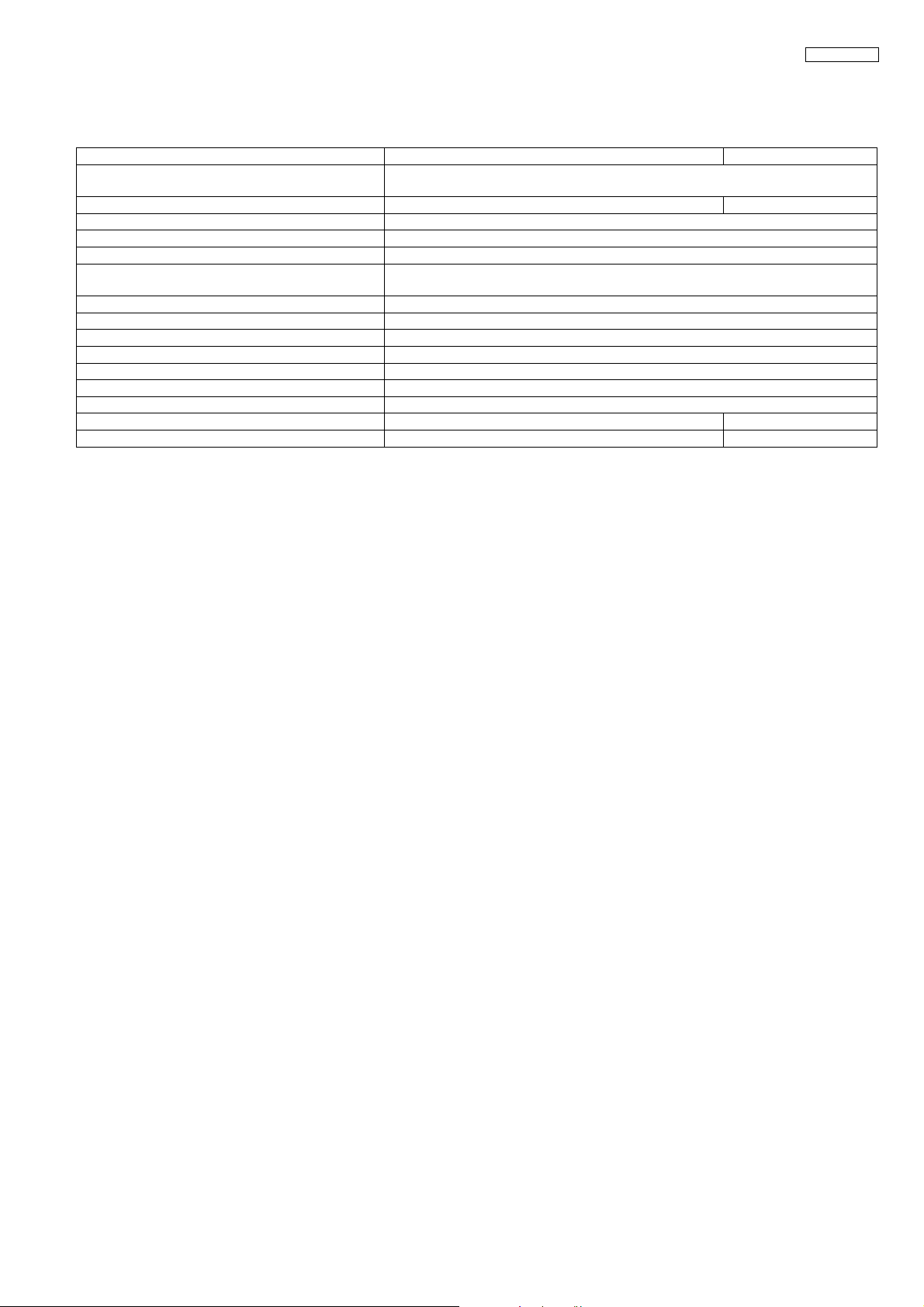
3 Specifications
Handset Charger Unit
Standard: DECT= (Digital Enhanced Cordless Telecommunications)
GAP= (Generic Access Profile)
Power Source: Rechargeable Ni-MH battery AC Adaptor
Number of Channels: 120 Duplex Channels
Frequency Range: 1.88GHz to 1.9GHz
Duplex Procedure: TDMA (Time Division Multiple Access)
Battery Life, Handset (if batteries are fully charged): Stand-by: Up to 200 hours (Ni-MH)
Talk: Up to 15 Hours (Ni-MH)
Channel Spacing: 1728kHz
Bit rate Spacing: 1152kbit/s
Operating Conditions: 5~40 °C, 20~80% relative air humidity (dry)
Modulation: GFSK= (Gaussian Frequency Shift Keying)
RF Transmission Power: approx. 250mW
Voice Coding: ADPCM 32 kbit/s
Operation Range: Up to 300 m outdoors, Up to 50 m indoors
Dimensions (D x W x L): 144 mm x 47 mm x 24 mm 85 mm x 76 mm x 39 mm
Weight: approx. 125g approx. 65g
5
Page 6

KX-TCA175UK
A
4 Technical Descriptions
4.1. Block Diagram (Handset)
Batt
Rear
Speaker
BBIC (SC14428F)
AFE DSP
BMC
1.8V
nt
3.0V
Receiver
Mic
Charge LED
LED(G)
3.0V
LED(R)
Key backlit
3.0V
LED(YG) Tr
J
a
c
k
H/S
detect
H
/
S
Tr
Tr
OP-Amp
Mic Bias
D/A
A/D
Batt
Peripheral
MIDI
Receiving
Calls
Making
Calls
RF I/F
Decoder
Encoder
CR16C
16
PWM
RFmodule
(DECT)
16
ACS0
16
ACS1
16
ACS2
Batt
RF 3.0V
Flash
(32Mbit)
SRAM
(2Mbit)
Color
LCD
Backlit
3.0V
3.0V
3.0V
5.0V
Charger
Circuit
Battery
3.6V
Charge Current
Charge on/off
Batt
Regulator
Power
Management
5.0V
RF 3.0V
Regulator
Batt
Keys
UART
JTAG
Xtal
10.368MH
3.0V
1.8V
KX-TCA175UK BLOCK DIAGRAM (HANDSET)
6
Page 7

4.2. Circuit Operation (Handset)
4.2.1. Outline
Handset consists of the following ICs as shown in Block Diagram (Handset) (P. 6 ).
• BBIC (Base Band IC): IC3
- All data signals (forming/analyzing ACK or CMD signal)
- All interfaces (ex: Key, Detector Circuit, Charge, LCD, LED, SRAM, Flash ROM)
• SRAM: IC1
- Application data and code are temporarily stored.
• Flash ROM (substitute EEPROM): IC2
- Source program data and temporary user data are stored.
• AMPLIFIER IC: IC5
- Single OP_AMP for SPEAKER
•RF Module:
- PLL Oscillator
- Detector
- Compress/Expander
- Amplifier for reception
- Amplifier for transmission
4.2.2. Power Supply Circuit/Reset Circuit
When power on the Handset, the voltage is as follows;
BATTERY(3.5 V to 4.2V: Battery+) → Q8 (1.8V) → Q10 (3.0V)
The reset signal is generated with IC3 and Q17.
Power for RF IC (IC601) is generated with IC603.
5.0V for LCD back-light is generated with IC4.
Battery (3.5V to 4.2V) is used for RF Module, Amplifier IC (IC605), DC/DC Converter (IC4).
1.8V is used only for BBIC (IC3).
3.0V is used for BBIC (IC3), LCD, SRAM (IC1), Flash ROM (IC2), Red LED, Green LED, Key back-light.
KX-TCA175UK
7
Page 8
KX-TCA175UK
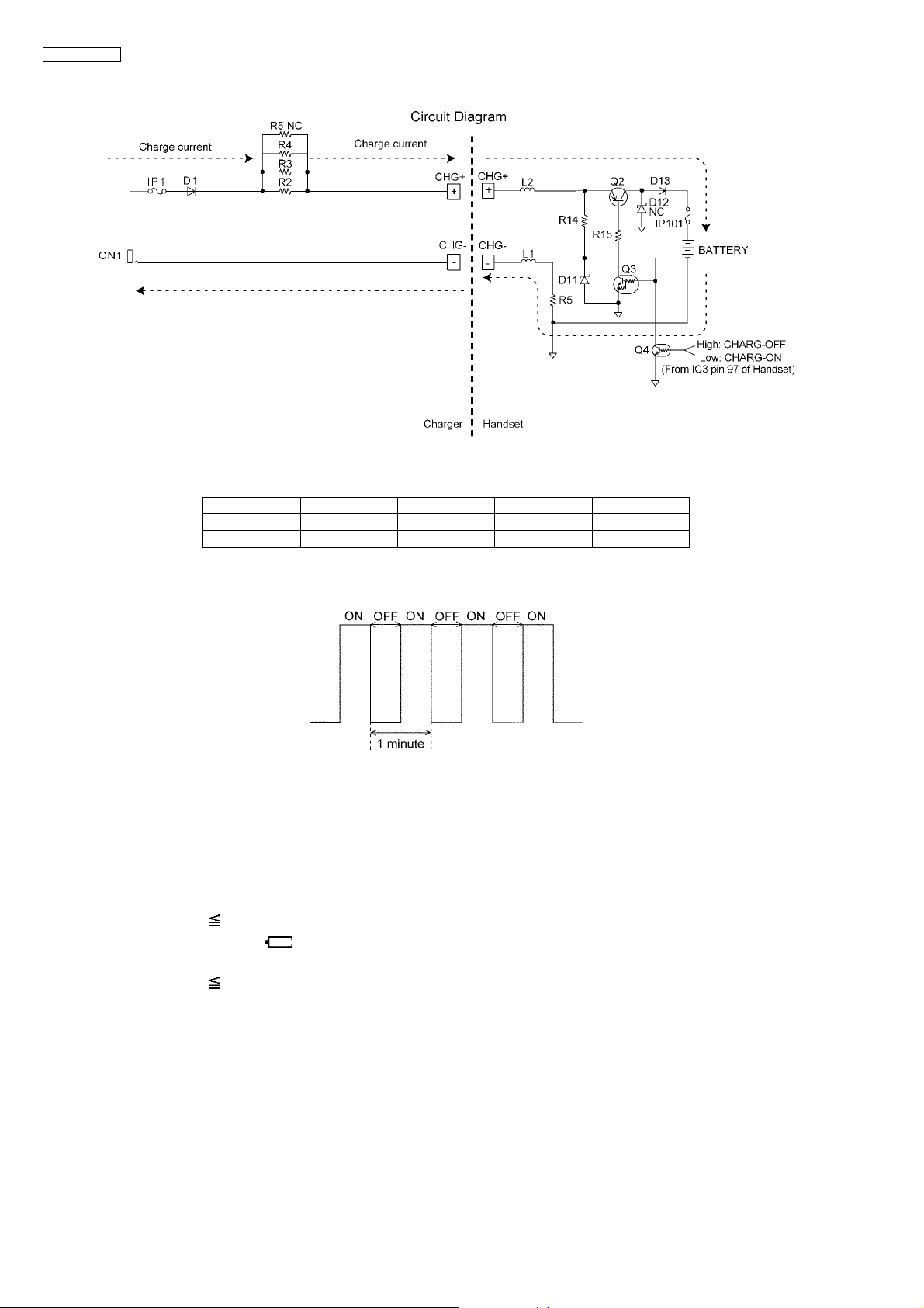
4.2.3. Charge Circuit (Include Charger)
• Charge current is controlled as follows.
IC3-97pin Q4 Q3 Q2
Charge ON Low OFF ON ON
Charge Off High ON OFF OFF
• Charge mode is trickle charge.
• Charge current repeats ON and OFF as follows.
• Charge route
DC+ (6.5V) → IP1 → D1 → R2, R3 and R4 → CHG+ (Charger) → CHG+ (Handset) → L2 → Q2 → D13 → IP101 → Battery →
GND → R5 → CHG- (Handset) → CHG- (Charger) → GND
4.2.4. Battery Low/Power Down Detector
"Battery Low" and "Power Down" are detected by BBIC (IC3) which checks the battery voltage.
The detected voltage is as follows;
• Battery Low
Battery voltage: V(Batt) 3.5V ± 50mV
The BBIC detects this level and " " starts flashing.
• Power Down
Battery voltage: V(Batt) 3.3V ± 50mV
The BBIC detects this level and power down.
8
Page 9

KX-TCA175UK
4.2.5. TX Audio Path
Microphone
An audio signal from microphone is input to pin 118 (MIC+) of IC3 via headset jack (CN1).
In IC3, the audio signal is converted from the analog signal to ADPCM, then to burst data, and sent from pin 28 (TXDA) to RF
Module. The stabilized supply voltage is fed to the microphone from pin 119 (VREF+) of IC3.
To reduce consumption current, this voltage is supplied only while calling or receiving.
Headset
When a headset is inserted, a signal from microphone is cut off and an audio signal from a headset is input to pin 118 (MIC+).
Headset detection
When a headset is inserted, pin 41 (ADC2) of IC3 goes from Low to High (around 1V) and BBIC (IC3) detects the insertion of
the headset.
9
Page 10

KX-TCA175UK
• LCD Circuit
• The LCD is controlled by 5 control signal (READ, WRT, A0, LCD_CS, LCD_RST) and Data bus.
• LCD back-light is controlled by IC3-79pin, and this PWM signal controls back-light brightness.
10
Page 11

KX-TCA175UK
4.2.6. RX Audio Path
Receiver
Burst data is input from RF Module to pin 26 (RXDA) of IC3.
In IC3, the burst data is converted to ADPCM, then to analog signal, and sent from pin 110 (LSR+) and pin 111 (LSR-) to the
receiver.
Headset
When the headset is inserted, a signal to the receiver is cut off and audio signal from pin 110 (LSR+) of IC3 is input to the
headset.
Speakerphone
In Speakerphone mode, the BBIC (IC3) makes pin 1 of IC5 from Low to High.
And an audio signal from pin 112 (LSR_HS) of IC3 is sent to a monitor speaker through speaker Amplifier IC (IC605).
11
Page 12

KX-TCA175UK
•LED Circuit
BBIC (IC3) controls each LEDs.
Call/Charge Indicator LED (Green), D1 IC3-81pin = High
Call/Charge Indicator LED (Red), D1 IC3-80pin = High
Key back-light LEDs (Yellow)
D3-D10, D17-D24
Type of LED LED ON LED OFF
IC3-81pin = Low
Q6 = ON
Q7 = ON
IC3-42pin = High
Q12 = ON
Q6 = OFF
IC3-80pin = Low
Q7 = OFF
IC3-42pin = Low
Q12 = OFF
4.2.7. Ringer Circuit
During ringing, a signal is sent from pin 112 of IC3 to a monitor speaker through speaker Amplifier IC (IC5). At this time, BBIC
(IC3) makes pin 1 of IC5 from low to high.
4.2.8. Key Click Sound Circuit
When the key is pushed, a signal is sent from pin 12 of IC3 to a monitor speaker through speaker Amplifier IC (IC5). At this
time, BBIC (IC3) makes pin 1 of IC5 from low to high.
12
Page 13
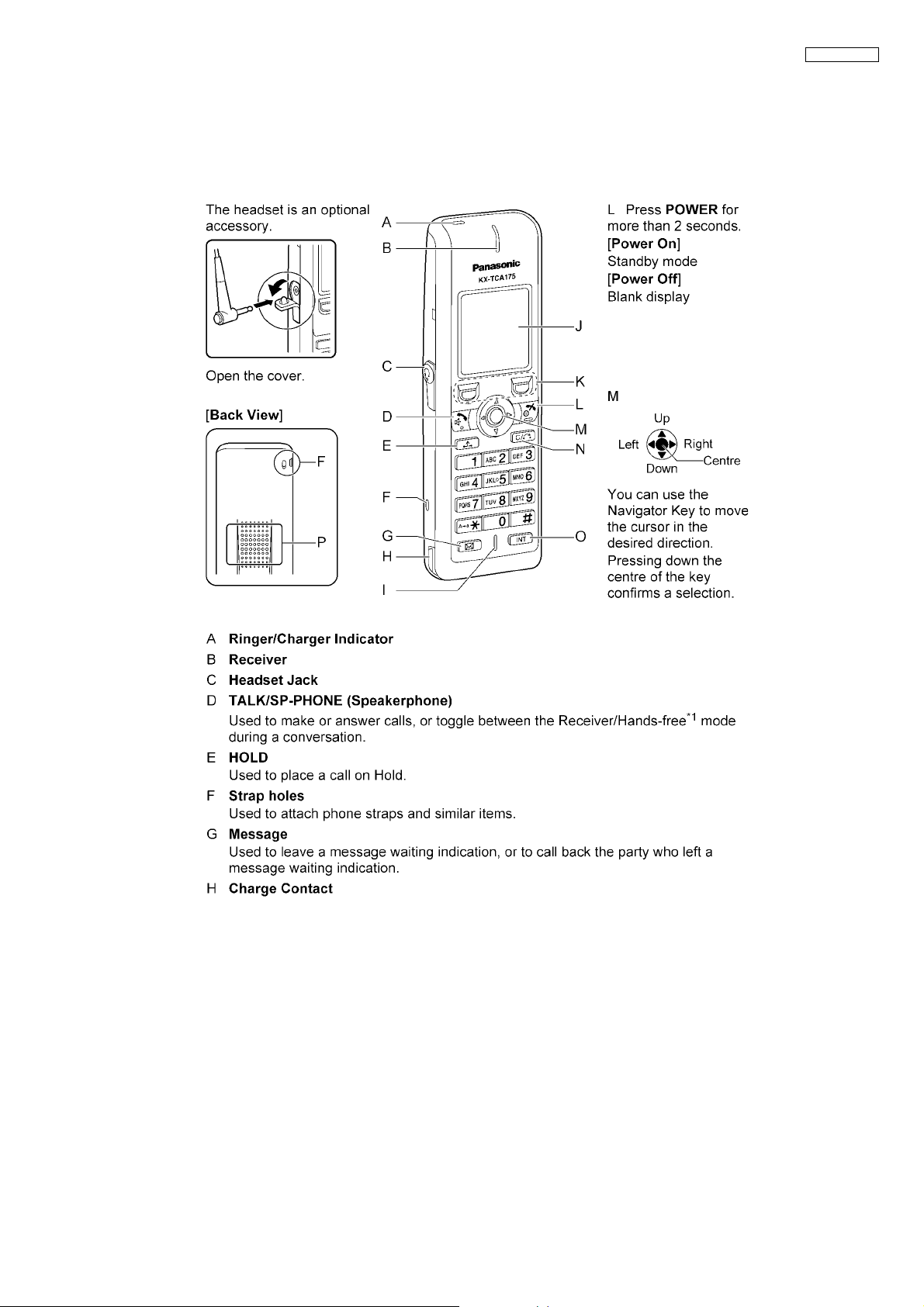
5 Location of Controls and Components
5.1. Handset
KX-TCA175UK
13
Page 14
KX-TCA175UK
14
Page 15
6 Installation Instructions
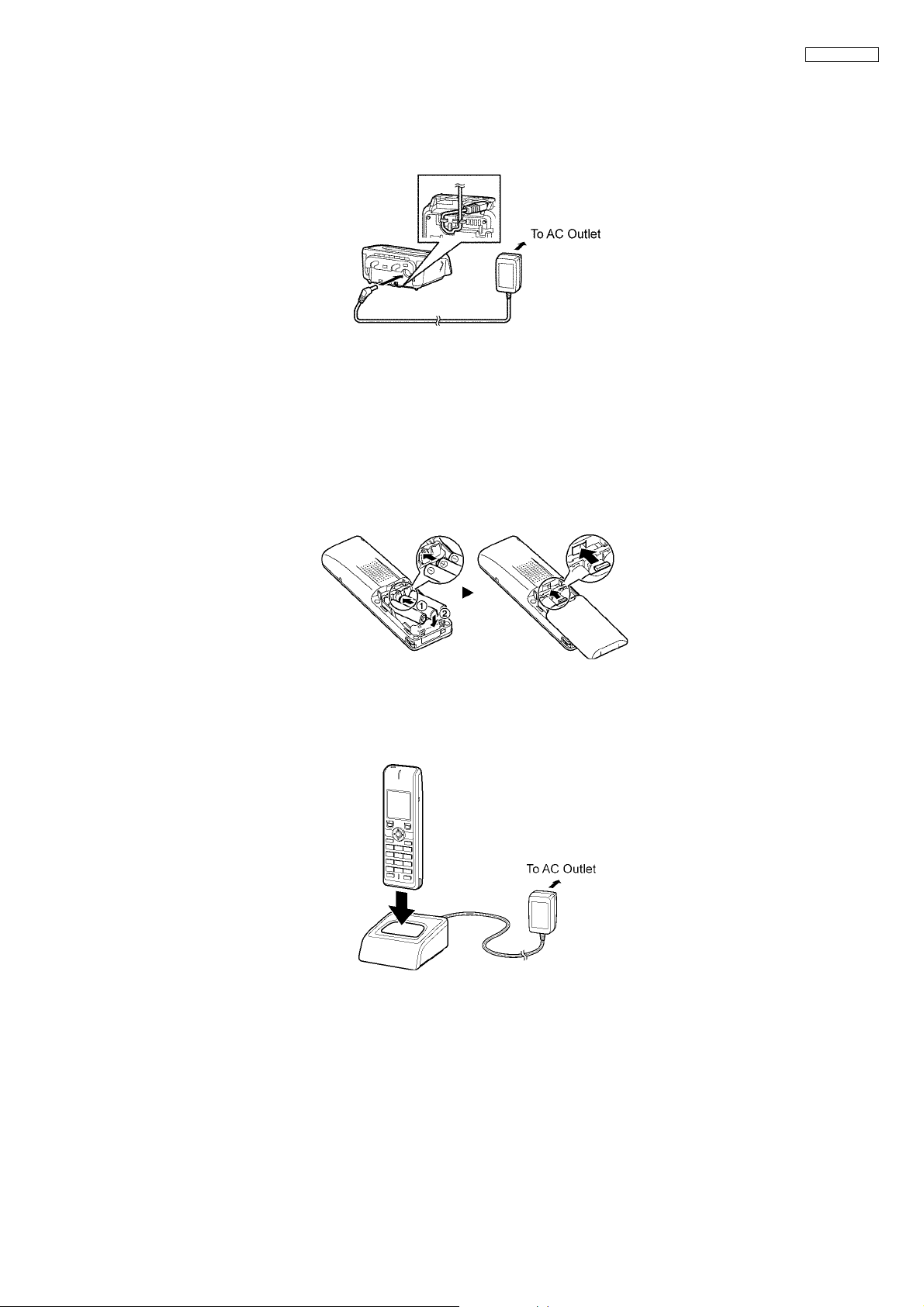
6.1. Charger Connection
Connect the AC adaptor to the charger.
• The AC adaptor should be connected to a vertically oriented or floor-mounted AC outlet.
Do not connect the AC adaptor to a ceiling-mounted AC outlet, as the weight of the
adaptor may cause it to become disconnected.
• Fasten the AC adaptor cord to the cord holder.
• Use only the included Panasonic AC adaptor (PQLV219E).
6.2. Battery
6.2.1. Battery Installation
Insert the batteries, and close the cover as indicated below.
KX-TCA175UK
6.2.2. Charging the Battery
At the time of shipment, the battery is not charged.
Please charge the battery for about 7 hours before using the handset for the first time.
• When the battery has been completely charged, the charge indicator will change from red to green.
• It is normal for the handset and charger to feel warm while the battery is charging.
• Keep devices sensitive to magnetic fields away from the charger.
• Use only the included charger.
15
Page 16
KX-TCA175UK
6.2.3. Battery Information
After your Panasonic battery is fully charged [at 25°C]:
Operation Operating Time
While in use (Talk) Up to about 15 h
While not in use (Standby) Up to about 200 h
• Operating time may be shorter than listed above depending on usage conditions and ambient temperature.
• The battery will drain slowly even while the handset is turned off.
• The handset can receive calls while charging.
• Battery consumption increases when the handset is used out of range. If " " flashes, turn the handset off.
6.2.4. Low Battery Warning
The battery needs to be charged in the following situations:
• “ “ flashes, and the alarm sounds*1.
• "Charge Battery" is displayed. In this situation, the handset cannot be operated.
*1 If the low battery warning occurs during a conversation, the call will be automatically disconnected one minute after the alarm
sounds.
6.2.5. Replacing the Batteries
If " "flashes after using the phone for a short time, even when the battery has been fully charged, the battery should be
replaced.
Before replacing the battery, make sure the low battery warning is displayed, then turn off the power to prevent memory loss.
Replace the battery and charge the new battery for about 7 hours.
If you replace the battery before the low battery warnings appears, the battery strength icon may display an incorrect reading. In
this case, use the handset as normal with the new battery installed. When the low battery warning is displayed, charge the battery for about 7 hours. The battery strength icon will then display the correct reading.
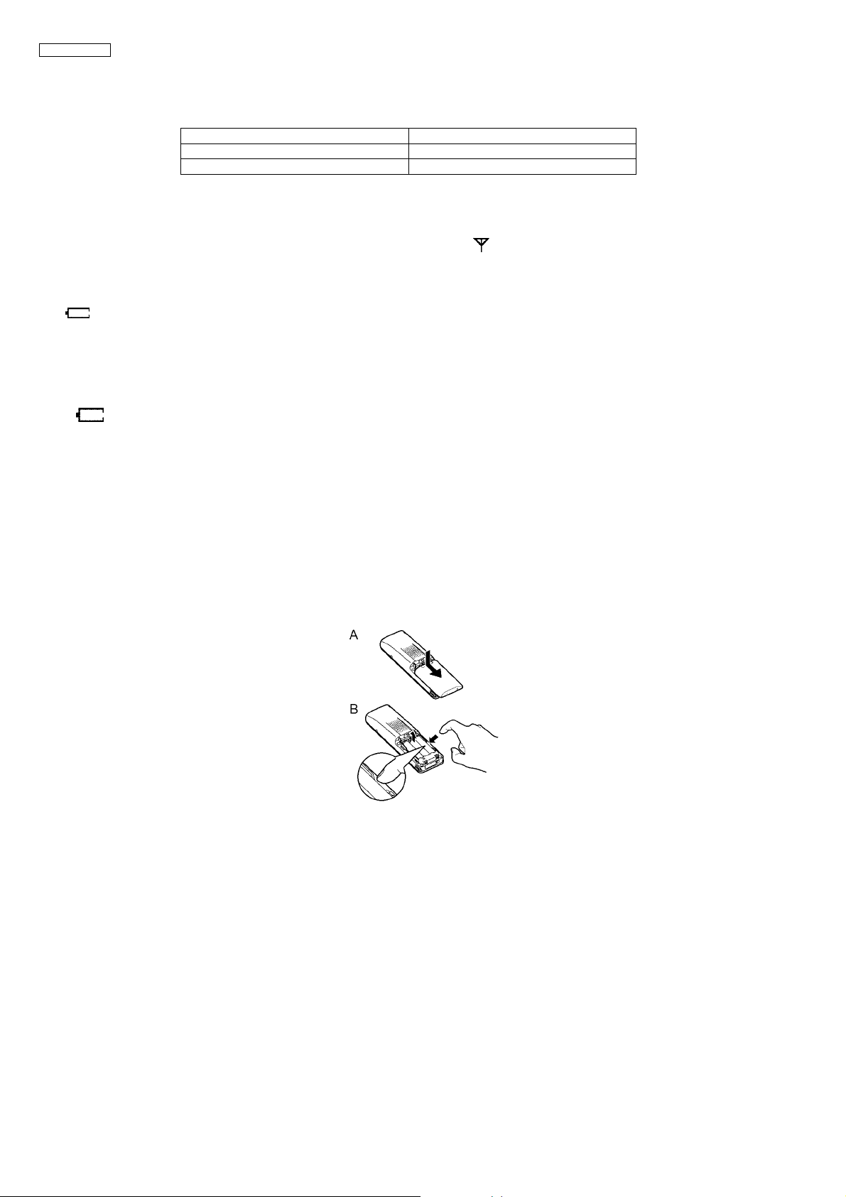
1. Turn the power off to prevent memory loss.
2. Press the notch on the cover firmly and slide it as indicated by the arrow (A).
3. Open the cover and replace the batteries.
• Insert a finger into the side gap to remove the batteries easily (B).
4. Close the cover and charge the handset.
• Please use a Panasonic battery with the service part number HHR-4EPT only.
16
Page 17
7 Operating Instructions
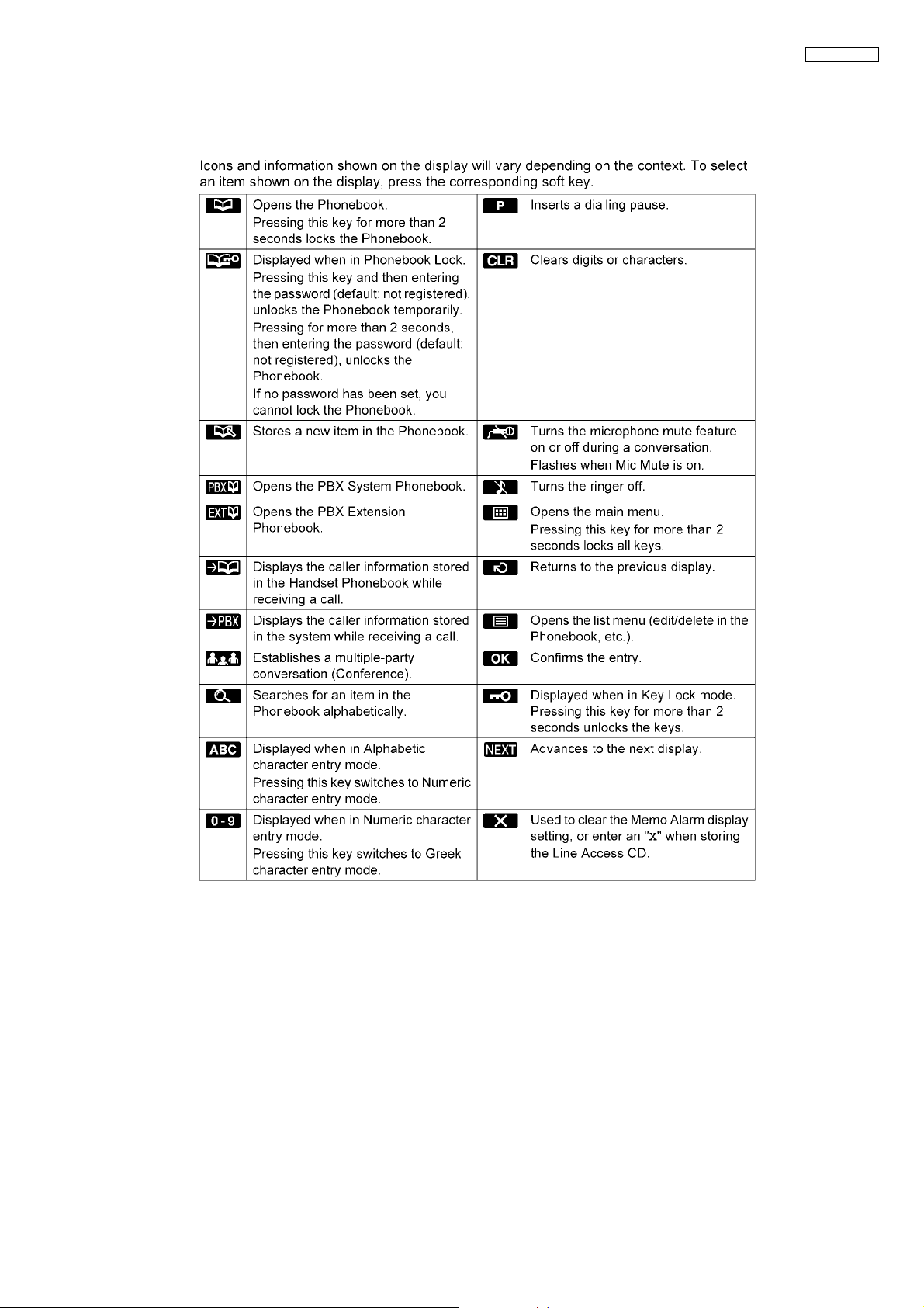
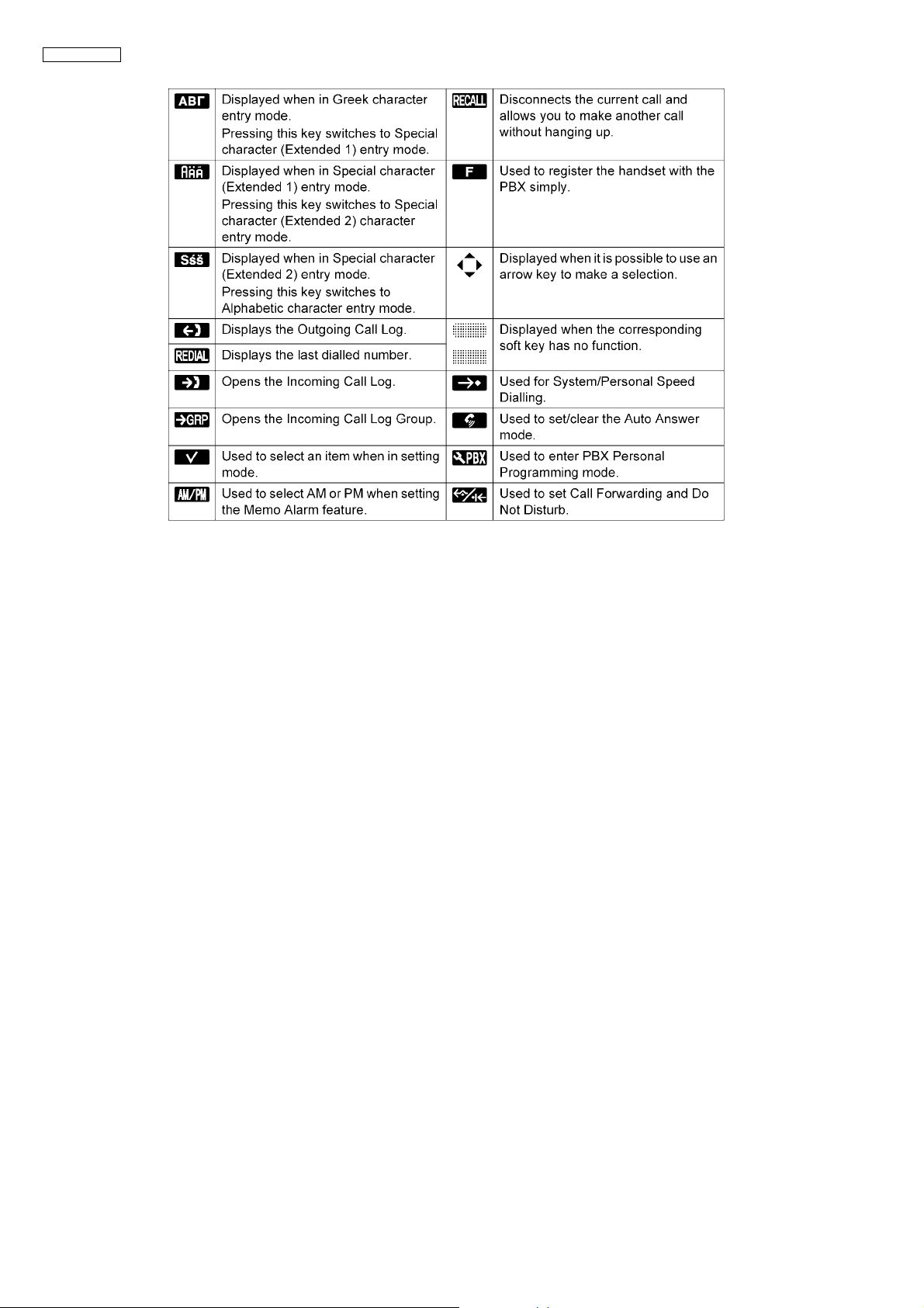
7.1. Soft Keys
KX-TCA175UK
17
Page 18
KX-TCA175UK
18
Page 19

7.2. Handset Setting Menu Layout
KX-TCA175UK
19
Page 20
KX-TCA175UK
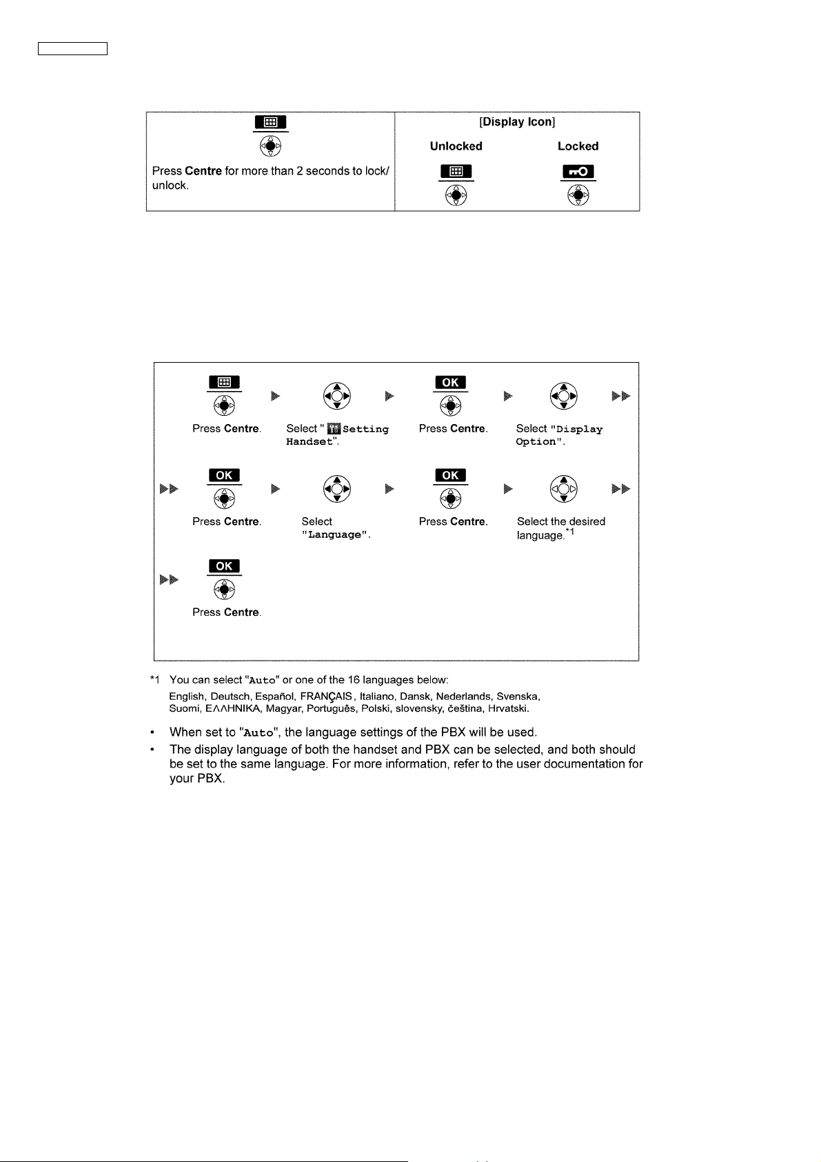
7.3. Key Lock
You can lock all keys other than the Navigator Key while the handset is in standby mode.
• If you select "Manual&Password" or "Auto & Password" for Key lock type, you need to enter the password for unlocking.
• If no password has been set, you cannot select "Manual & Password"or "Auto & Password" for Key lock type.
7.4. Selecting the Display Language
You can select the language displayed on your handset.
20
Page 21
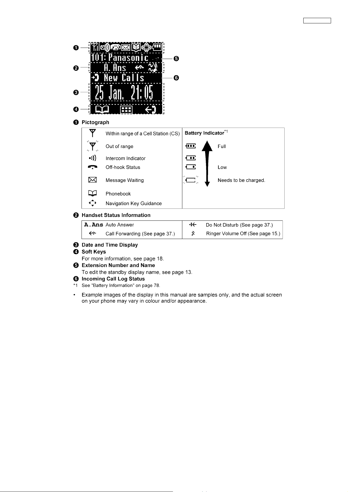
7.5. DISPLAY
KX-TCA175UK
21
Page 22
KX-TCA175UK
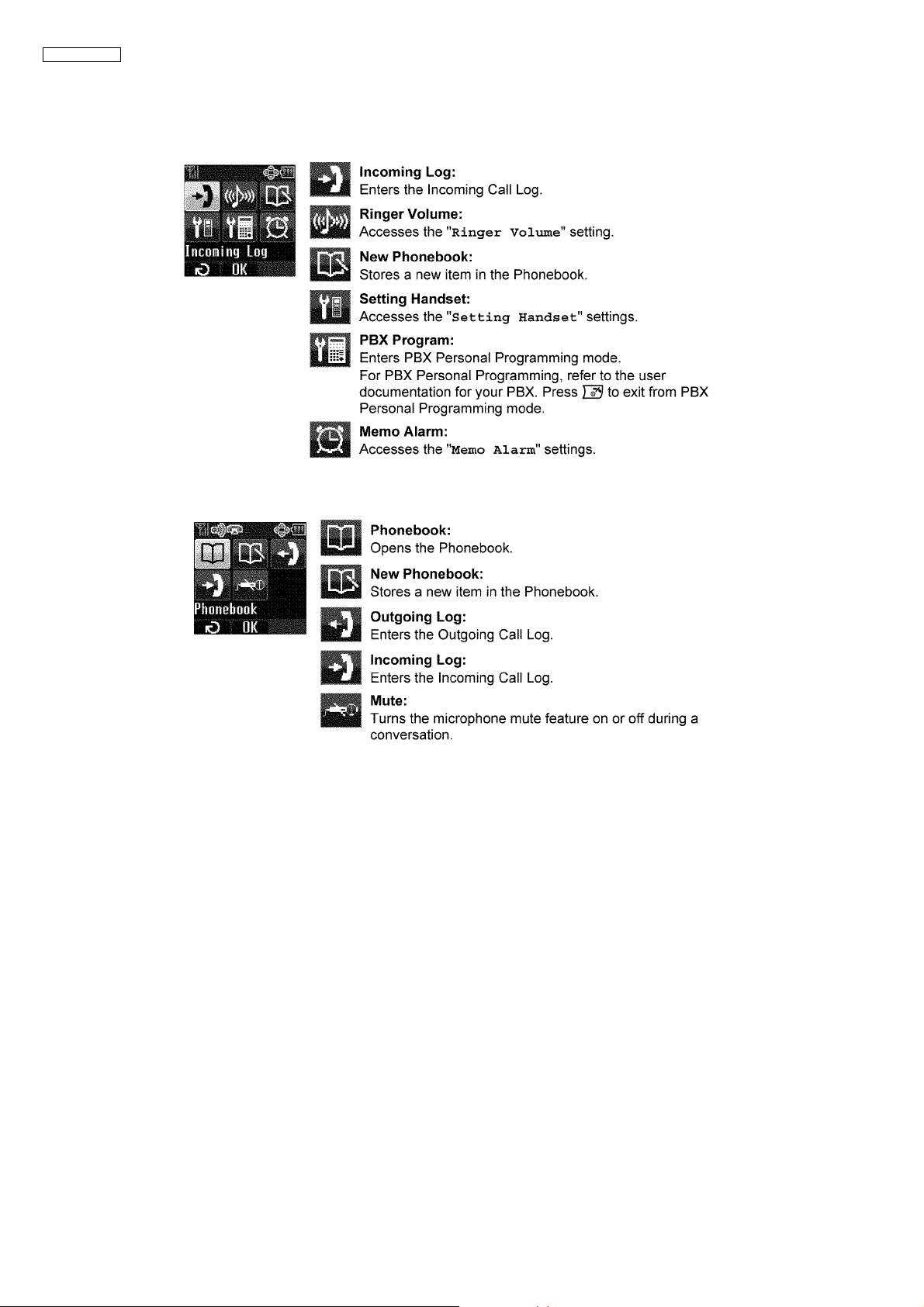
7.6. Function Menus
Press the Navigator Key to display the main and sub menus.
7.6.1. Main Menu-While in Standby Mode
7.6.2. Sub Menu-While Off-hook/During a Conversation
22
Page 23

7.7. Function Keys
KX-TCA175UK
23
Page 24

KX-TCA175UK
7.8. Flexible Keys
24
Page 25
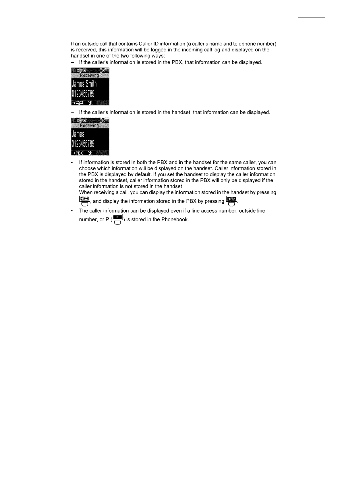
7.9. Caller ID
KX-TCA175UK
25
Page 26

KX-TCA175UK
7.10. Character Mode Table
26
Page 27

8 Troubleshooting Guide
KX-TCA175UK
Note:
When you find the suspected parts, check the soldering and resolder or replace the parts if it is necessary.
27
Page 28

KX-TCA175UK
8.1. Power Trouble (Handset)
8.1.1. Power Does Not Go On
The symptom is No Lite (LED OFF), No Display, No Sound.
28
Page 29

• Charger Unit
• NO Display On the LCD
KX-TCA175UK
29
Page 30
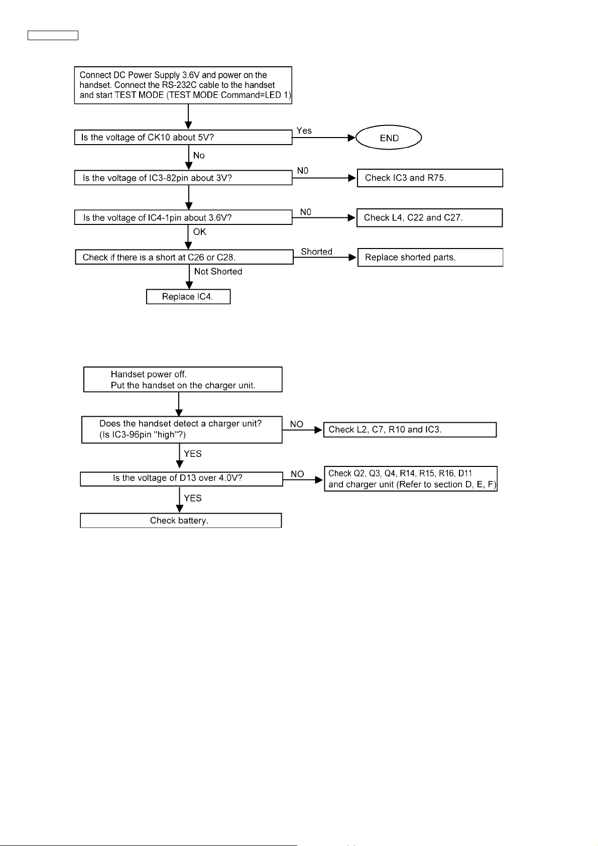
KX-TCA175UK
• 5V Circuit
8.2. Battery Charge Trouble (Handset)
8.2.1. Charge On
30
Page 31

8.2.2. Charge Off
KX-TCA175UK
31
Page 32

KX-TCA175UK
8.3. LED Trouble (Handset)
8.3.1. Key Back-Light
8.3.2. Charging And Ringing LED
32
Page 33
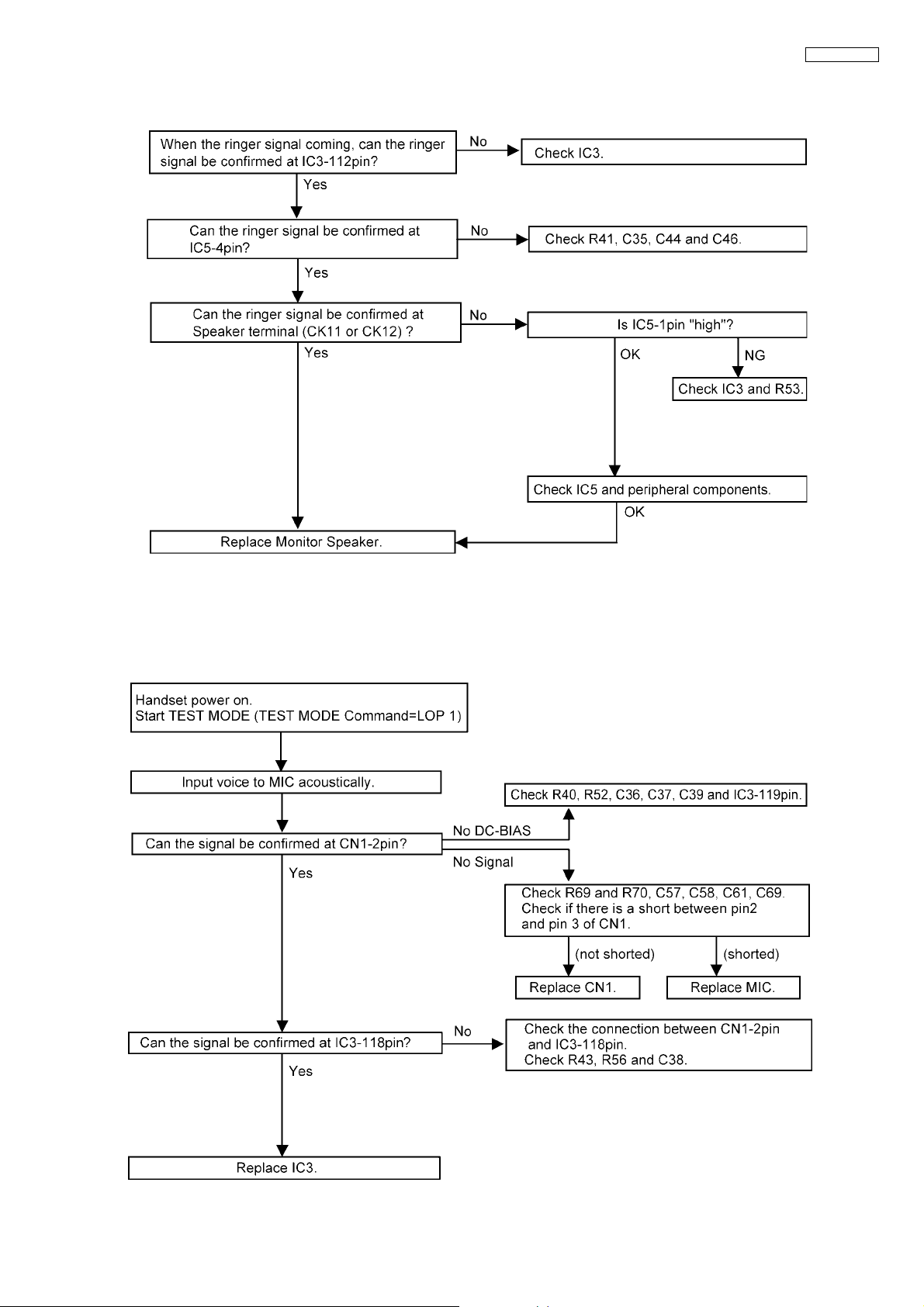
8.4. Ringer Trouble (Handset)
Check ringer volume setting and setting at first.
KX-TCA175UK
Key Click Sound Troubleshooting is same method.
Check Keyfone setting of handset at first.
8.5. No Voice Transmission
33
Page 34

KX-TCA175UK
8.6. No Voice Reception
8.6.1. Talk Mode
34
Page 35

8.6.2. Speakerphone Mode
KX-TCA175UK
8.7. Password Trouble
8.7.1. User Password is forgotten.
Test command "PWC" set user password to "1234".
8.7.2. System Lock Password is forgotten.
Test command "SLC" unlock the system lock.
35
Page 36
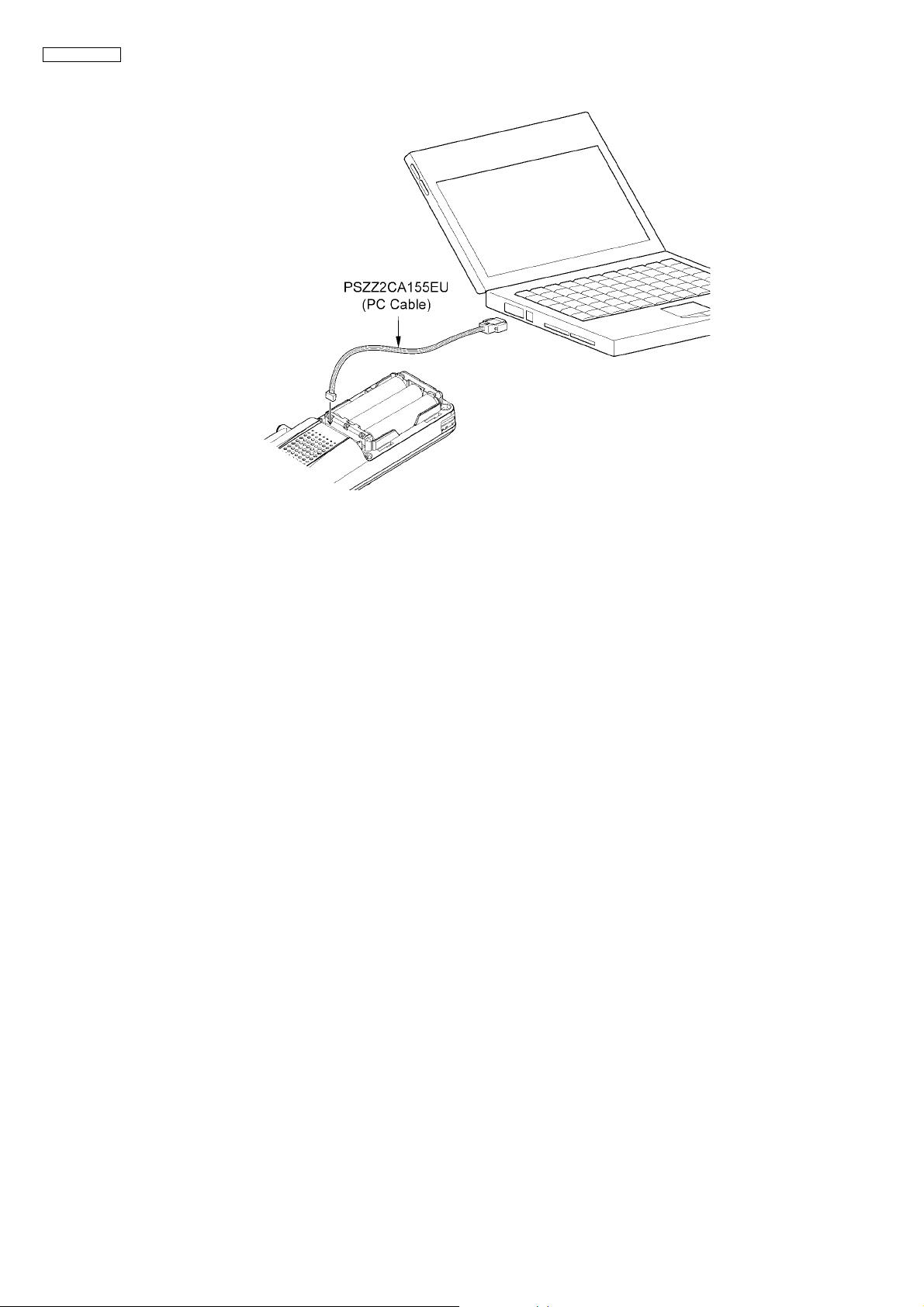
KX-TCA175UK
9 Service Fixture & Tools
36
Page 37
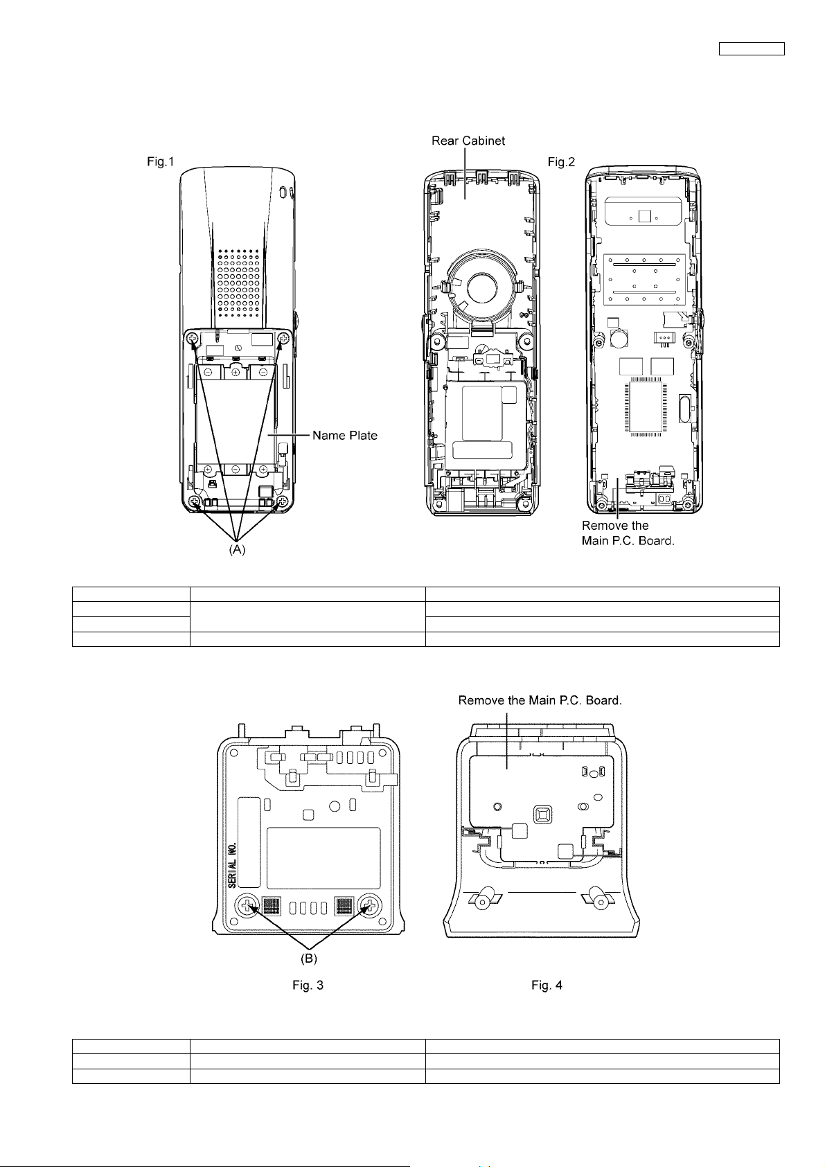
10 Disassembly and Assembly Instructions
10.1. Handset
KX-TCA175UK
Shown in Fig.- To Remove Remove
1 Rear Cabinet Screws (2 × 8)..........(A) × 4
2 Follow the procedure.
3 Main P.C. Board Main P.C. Board
10.2. Charger Unit
Shown in Fig.- To Remove Remove
4 Lower Cabinet Screws (2.6 × 12)..........(B) × 2
5 Main P.C. Board Main P.C. Board
37
Page 38

KX-TCA175UK
11 Measurements and Adjustments
11.1. Check Procedure (Handset)
11.1.1. Preparation
11.1.1.1. Equipment Required
• DECT tester: Rhode & Scorers, CMD 60 is recommended.
• Frequency counter: it must be precise to be able to measure 1Hz (precision; ±4ppm).
Hewlett Packard, 53131A is recommended.
• DC power: it must be able to output at least 1A current under 3.8V for Handset, 9V for Tool.
• Digital multi-meter (DMM): it must be able to measure voltage and current.
• Oscilloscope
11.1.1.2. Tool and PC
• EEPROM serial Tool
Tool: PSZZ2CA155EU
• PC which has “flash program.exe”.
11.1.2. PC Setting
11.1.2.1. Connections
38
Page 39

11.1.3. Download Manual
11.1.3.1. Step [1] Before Downloading (Configuration Setting)
[1]-(1) Execute "Flash Program.exe"
KX-TCA175UK
11.1.3.2. [1]-(2) Press Config
[1]-(3) Press OK
Selected item will be stored.
Connect the download PC cable with selected come port (COM1-COM9).
39
Page 40

KX-TCA175UK
11.1.3.3. Step [3] Select Download file
[3]-(1) Download Program Main Menu
Push "Reference" to select the download file. (Download Filename tca275vXXX.hex) XXX=Version
Select [program All] for [erase type].
40
Page 41
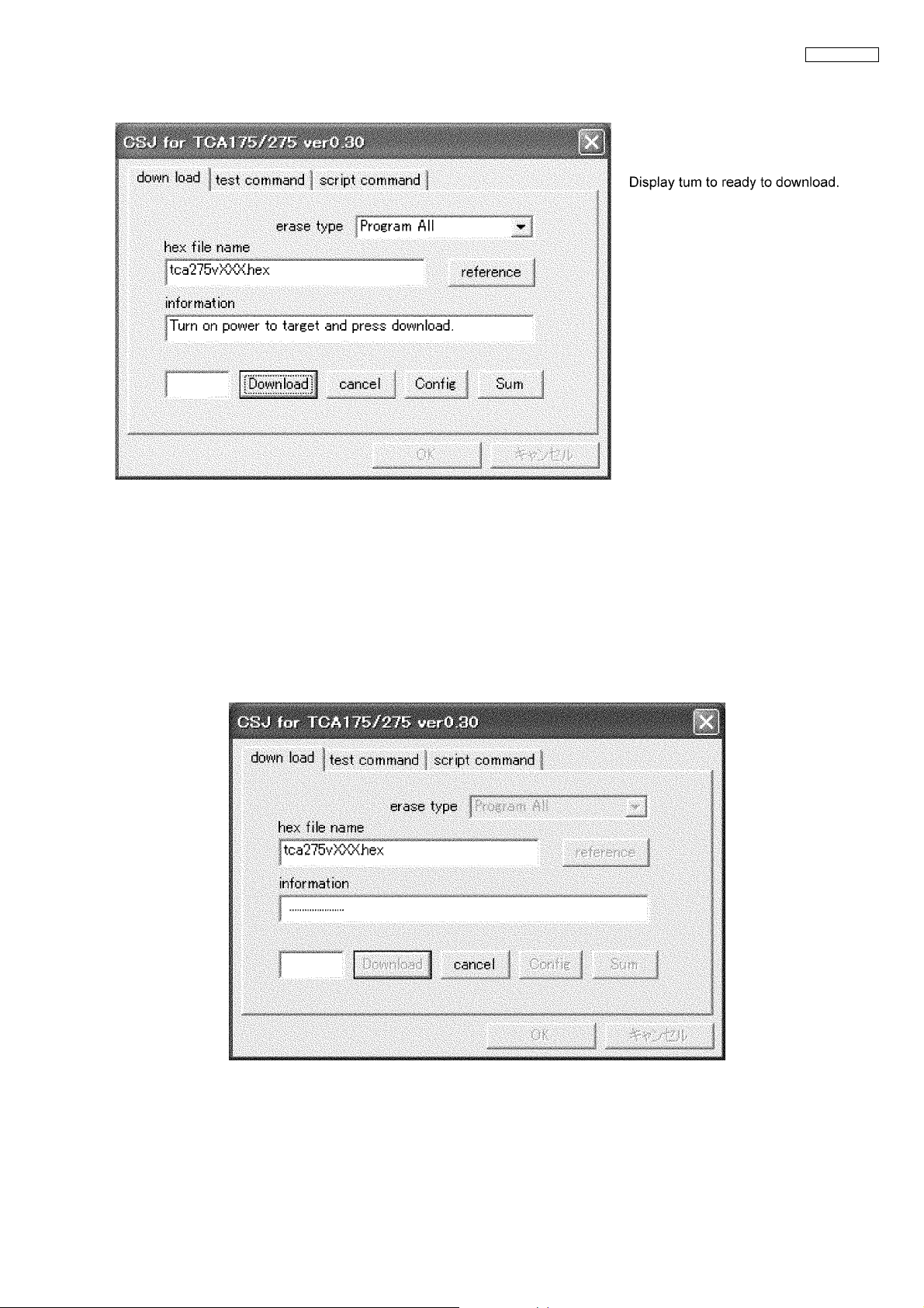
11.1.3.4. Step [4] Download Start
[4]-(1) Click "download" key
[4]-(2) Turn the power of target (TCA275) to [OFF]
(Keep pressing "POWER" key for while 2 seconds)
[4]-(3) Keep pressing "POWER" key until step [4]-(6)
This operation will not turn the power of target to on.
If target power turns on, check following item. Then try again from step [1]-(1).
(A) Check serial PC cable connection "PC" with "TCA275".
(B) Check Configuration. (Refer to Step [1]-(2))
(C) Check PC cable attachment of target.
[4]-(4) Click "Download"
Communicating PC with Target.
Don't release the "POWER" key in this step. If release the "OFF" key, downloading will be failed.
KX-TCA175UK
41
Page 42
KX-TCA175UK
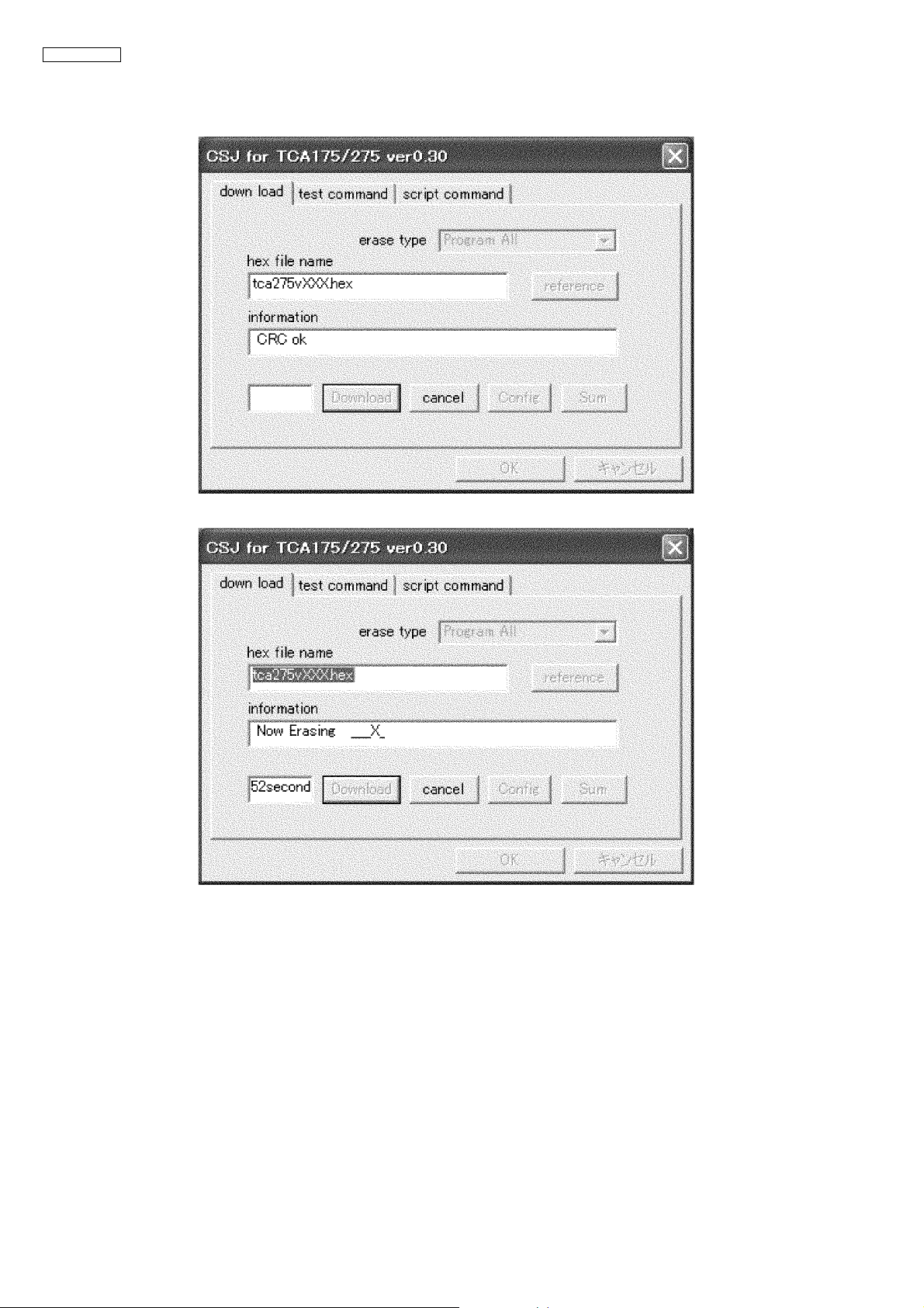
[4]-(5) Communication check "OK"
If communication check become "OK", Display will show "CRC OK".
If communication NG, click "cancel" key, then back to step [4]-(1) and try download again.
Erase the flash ROM.
You can release the "POWER" key in this step.
42
Page 43
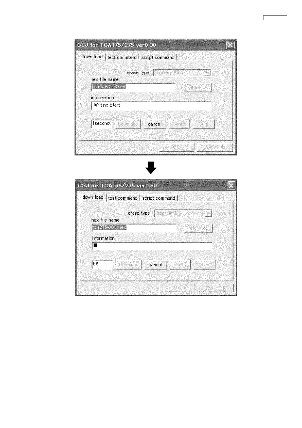
[4]-(6) Downloading Start
After several seconds, Display shows "Flash Program Start".
KX-TCA175UK
43
Page 44

KX-TCA175UK
[4]-(7) Downloading Complete
If downloading finished, display shows "Download finished successfully!".
Click "OK" then disconnect the serial PC cable.
11.2. Adjustments (Handset and Charger Unit)
11.2.1. Adjustment (Handset)
When you change IC3, you must adjust (A)(F)(H)(I)(K)
Items Adjustment
Point
(A)* 1.8V Supply Confirma-
tion
(B) 3V Supply Confirmation CK18 1. Confirm that the voltage between "CK18" and GND is 3.0V±0.15V. IC3, Q10,
(C)* Software Confirmation - 1. BBIC Confirmation (Execute the command "SLF", and “VER”).
(D) Charge Control Check &
Charge Current Monitor
Confirmation
(E)* Charge Detection (OFF)
Confirmation
(F)* Battery Monitor Confir-
mation
CK17 1. Confirm that the voltage between test point "CK17" and GND is 1.8V±0.02V.
2. Adjust the 1.8V voltage of CK17 executing command "VDD XX" (XX is the
value).
2. Confirm the returned checksum value.
Connection of checksum value and software version is shown below.
- 1. Apply 6V between CN3(+) and CN4(-) with current limit of PSU to 200mA.
2. Confirm that the charge current is ON/OFF.
3. SW to decrease current limit of PSU to 100mA.
4. Confirm that the charge current is stable.
- 1. Stop supplying 6V to CN3(+) and CN4(-).
2. Execute the command "BTS".
3. Confirm that the returned value is 0x00 (hex).
- 1. Apply 3.5V ± 0.02V between BATT(+) and BATT(-).
2. Execute the command "LED 0", then "AD1".
3. Confirm:
20 returned value 38 (Hex)
4. Adjust the Battery Monitor executing command.
(XX=returned value, YY=XX-9(hex))
WB2 XX
WB4 XX
WB3 YY
Procedure* Check or
Replace Parts
IC3, Q8, R26
R28, R32, R33
IC3, X1, C13,
C17, R88
(IC1, IC2)
IC3, R5,
Q2, Q3, Q4,
L1, L2, R10,
R14, D11,
D13, R15, R16
IC3, R10, R5,
L1, L2, C7
IC3,
R35, R38
44
Page 45
KX-TCA175UK
Items Adjustment
Point
(G) Battery low Confirmation - 1. Apply 3.55V between BATT(+) and BATT(-).
(H)* BBIC Clock Adjusment SYRI 1. Execute the command "RFC 1".
(I)* Modulatoin Check and
Adjusment
(J)* RSSI Level Confirmation - Follow steps 1 to 3 of (I) above.
(K) RSSI Calibration Confir-
mation
(L) Country setting 1. Excute the command "DCS 1"
- 1.Set RFPI to 0102030405 in CMD60.
- 1. Set DECT Tester Power to -93dbm.
2. Confirm that there is no flashing of Battery Icon.
3. Apply 3.4V between BATT(+) and BATT(-).
4. Confirm that there is flashing of Battery.
2. Adjust the frequency of SYRI executing the command "SFR xx (where xx is
the value)" so that the reading of the frequency counter is 10.368000MHz
±10Hz.
2.Excure the command “TST 01 02 03 04 05”.
3.Press “Set up connection” at CMD 60.
4.Confirm that the B-Field Modulation is 360kHz/div~380kHz/div using data
type Fig 31.
5.Adjust the B-Field Modulation if required. (Execute the command "SMR xx",
where xx is the value.)
4.Set DECT tester power to -93dBm.
5.Execute the command "RSS".
6.Confirm that the returned value is 0x8±8 (hex).
7.Set DECT tester power to -63dBm.
8.Execute the command "RSS".
9.Confirm that the returned value is 0x1D±8 (hex).
2. Run "RSS" and record the returned value.
3. Run follwing command and verify the value xx is returned value is step2.
EPW 00 69 1 XX
EPR 00 69 00 01
4. Set DECT Tester Power to -63dbm.
5. Run "RSS" and record the returned value.
6. Run follwing command and verify the value xx is returned value is step5.
EPW 00 6A 1 XX
EPR 00 6A 00 01
Procedure* Check or
Replace Parts
IC3,
R35, R38
IC3, X1, C17,
C13, C14, L3,
R23, R88
RF module
IC3,
RF module
IC3,
RF module
IC3, CN5,
R6-9, R11,
R12
Note:
Execute 3 command "MCW", "BWP","M2B 0" in order after adjustment.
If not, handset display shows error message after turning on again.
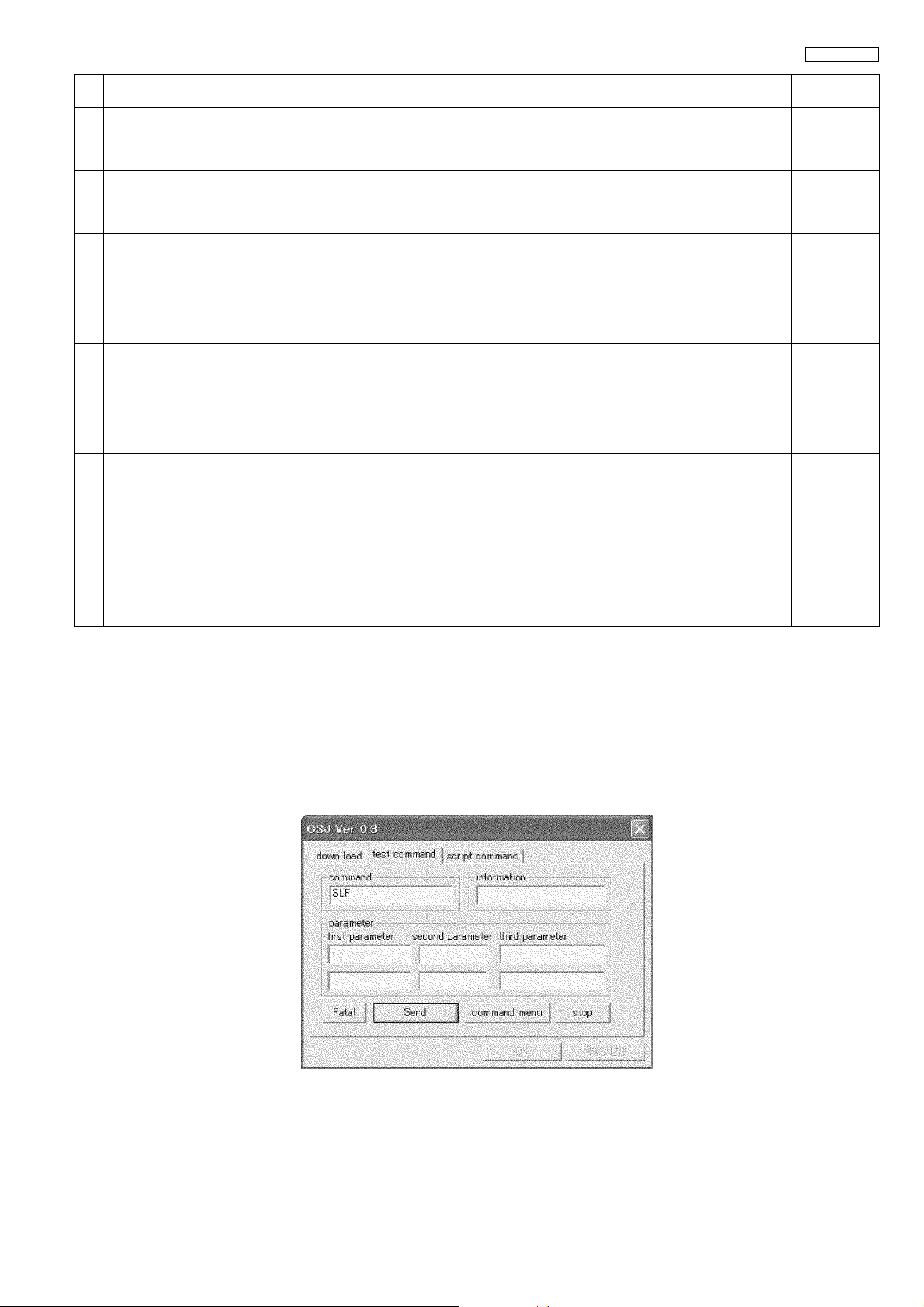
1) Run "Flash Program.exe"
2) Select "test command" sheet.
3) Enter command in command column.
4) Press "Send" button.
45
Page 46

KX-TCA175UK
11.2.2. Adjustment Standard (Handset)
When connecting the Simulator Equipments for checking, please refer to below.
POS1
C674
AF VOLT METER
OSCILLOSCOPE
DIGITAL
VOLTAGE METER
DC POWER
SUPPLY for charge
DC POWER
SUPPLY
CK10
CK17
CK18
8Ω
R53
C40
C41
R24
R603
C606
L601
C677
1
D25
C44
Q7
L4
R1
C27
R37
R26
C22
C28
C29
L1
R613
C605
R3
Q6
C26
IC4
R29
R75
Q8
L630
R607
C622
C609
L602
C603
C604
FB606
C684
IC603
IC605
C46
R4
R25
Q1
R9
R73
R11
Q17
C5
CHG-
R606
C621
C601
C682
C675
R605
C620
IC601
R615
C632
Br
R67
C60
C54
C49
C683
R41
C53
C48
R614 R611
C624
R610
L608
C67 C62
C73
C56
R58
PbF
R608
C623
C608
C607
C681
C610
R604
C630 C633
C631 L606
C108
PSUP1709Z -A
IC2
R86
R8
R6
R18
C9
C10
R31
R39
R30
D16
R36
C72
Q11
R33
R32
C19
R34
R5
R28
Q10
C4
C109
D15
C25
BATT-
C20
R38
C30
C12
R35
R72
R70
R612
C625
R626
FB603
C626
C627
R645
C65
R64
R59
R65
R89
R57
C1
R87
C8
IC3
C21
D13
C36
C37
MIC
W
SPK
C69
C691
C634
C35
R56
R43
C24
R69
L632
R42
Q14
C23
C58
TP601
C660
L617
C665
L621
D602
L620
C649
R632
C648
C646
C647
C643
C645
IC602
C642
C651
R623
C690
C75
R66
C64
C31
C57
C74
Q13
R60
C59
IC1
C2
R27
R40
C39
C38
R52
C61
IP101
BATT+
Bk R
FIL601
L616
D601
C699
CN5
C68
C63
C11
D11
R16
C7
R10
C654
R21
C15
R23
C18
C110
VIB
C666
C657
C678
C656
L631
CN1
C70
R71
C66
C55
C122
R55
R7
C13
R88
C16
L3
C14
Q12
R20
Q3
Q4
R13
C6
C673
JP601
C670
C650
R625
C653
C680L611C652
L615
L610
L614
C672
R634
R633
L605 L603
C671
PSZZ2CA155EU
R62
R54
R63
R68
C52
C51
R61
R74
IC6
C50
C47C45
C17
X1
R42
C33
C34
R17
R22
Q5
R21
R15
Q2
R14
L2
CHG+
A
D14
C43
SYRI
10uF
TP601
GND
AF
10uF
OSC
FREQUENCY
COUNTER
150Ω
PC
AF OSC
AF VOLT
METER
OSCILLO
SCOPE
KX-TCA175UK CIRCUIT BOARD Component View
46
Page 47
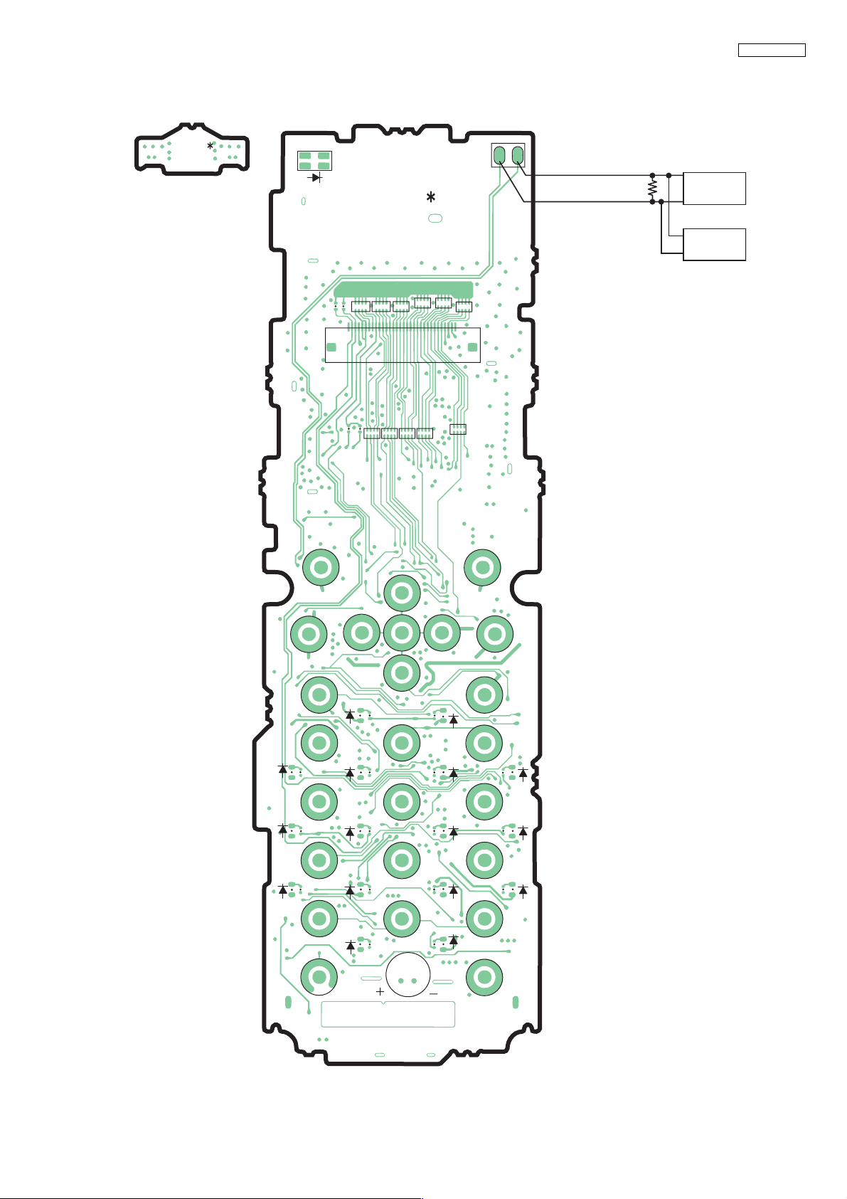
KX-TCA175UK
PSUP1709Z -B
PbF
D1
PSUP1709Z -A
C121
C120
RA10RA11
1
R2
C3
RA5 RA4 RA3 RA2
RA9
CN2
Bk R
RECV
110Ω
AF VOLT
METER
OSCILLO
SCOPE
RA7RA8
RA6
RA1
D19
D20
D21
SW01
R78
R79
R80
SW11
SW31
SW21
SW51
SW53
SW03
SW33
SW00
D3
D5
D7
D9
D17
SW10
SW30 SW20
SW50
R44
SW52
R46
SW02
R48
SW12
R50
SW13
R76
R47R45
R49
R51
R77
D4
D6
D8
D10
D18
SW40
SW41
SW42
SW32
SW22
SW23
SW43
SW1
R81
R82
R83
D22
D23
D24
A
KX-TCA175UK CIRCUIT BOARD Bottom View
47
Page 48
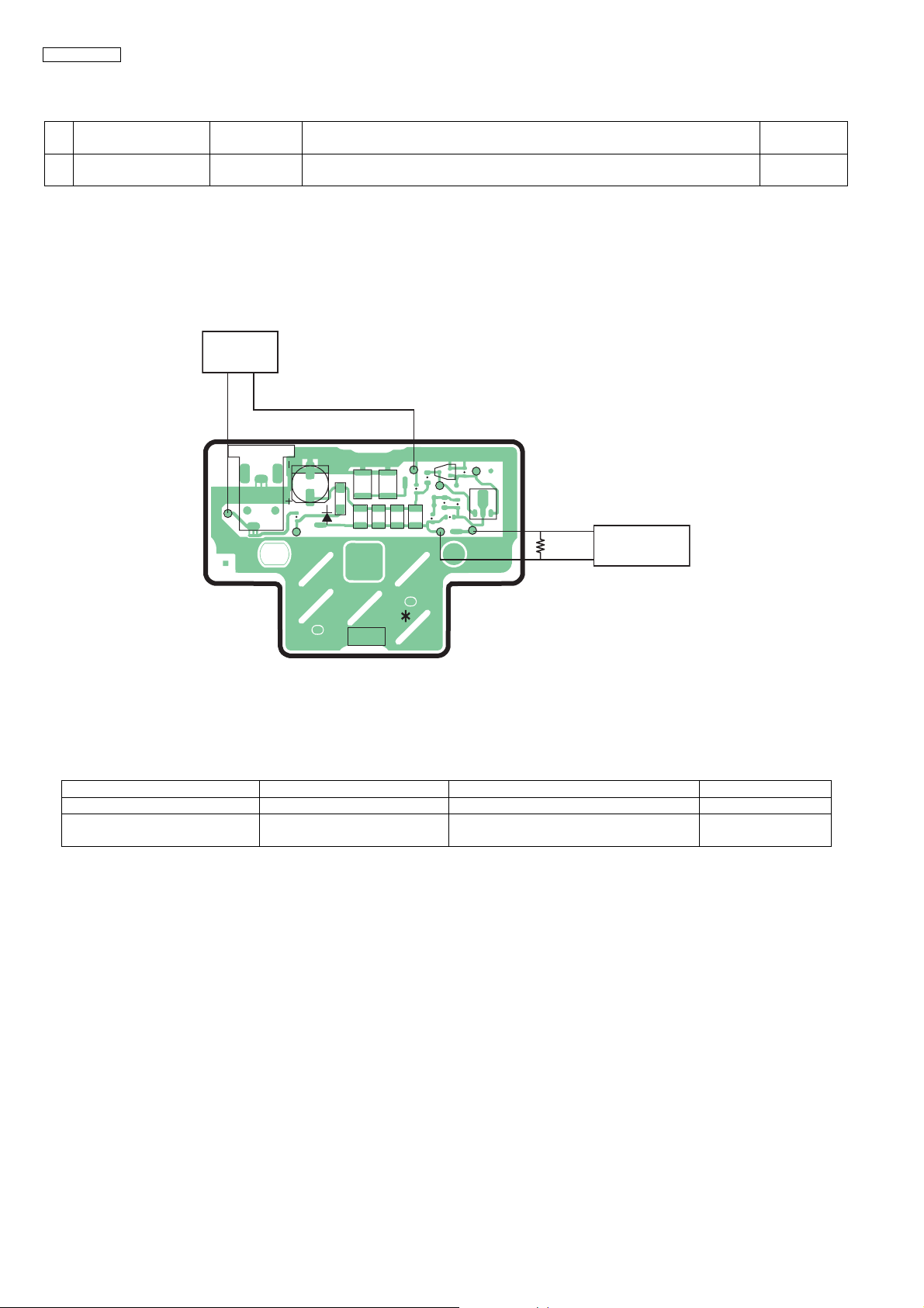
KX-TCA175UK
11.2.3. Adjustment (Charger Unit)
Items Adjustment
Procedure Check or
Point
(A) Charging Check - 1. Connect Charge Contact 30Ω/2W register between charge+ and charge-.
2. Measure and confirm voltage across the register is 5.0V±0.2V.
Note:
After the measuring, sock up the solder of TP.
11.2.4. Adjustment Standard (Charger Unit)
When connecting the Simulator Equipments for checking, please refer to below.
11.2.4.1. Flow Solder Side View
DC POWER
6.5V
GND
CK1
CN1
IP1
CK3
CK2
C1
R6
R7
CK4
D1
C2
R5R4R3R2
CK6
C3
CK5
Q1
R1
Q2
R8
C4
C5
C6
CK7
GND
30Ω
2 Watts
Digital Volt Meter
Replace Parts
PSUP1712Z
PbF
KX-TCA175UK CIRCUIT BOARD
(CHARGER UNIT) Component View
A
11.3. RF Specification (Handset)
Item Value Refer to -. ** Remarks
Modulation 360 kHz/div~380 kHz/div Adjustment (Handset) (I) Data type: Fig31
RSSI Level 0x08 hex±8 hex (at -93dBm)
0x1D hex±8 hex (at -63dBm)
**: Refer to Adjustment (Handset) (P.44)
Adjustment (Handset) (J)
48
Page 49

11.4. How to Check the Handset Speaker
1. Prepare the digital voltmeter, and set the selector knob to ohm meter.
2. Put the probes at the speaker terminals as shown below.
KX-TCA175UK
11.5. How to Check the Handset Receiver
1. Prepare the digital voltmeter, and set the selector knob to ohm meter.
2. Put the probes at the receiver terminals as shown below.
49
Page 50

KX-TCA175UK
11.6. Frequency Table (MHz)
Channel No Transmit / Receive Frequency
0 1897.344
1 1895.616
2 1893.888
3 1892.160
4 1890.432
5 1888.704
6 1886.976
7 1885.248
8 1883.520
9 1881.792
50
Page 51

KX-TCA175UK
12 Miscellaneous
12.1. How To Replace a Flat Package IC
Even if you do not have the special tools (for example, a spot heater) to remove the Flat IC, with some solder (large amount), a soldering iron and a cutter knife, you can easily remove the ICs that have more than 100 pins.
12.1.1. Preparation
• PbF (: Pb free) Solder
• Soldering Iron
Tip Temperature of 700°F ± 20°F (370°C ± 10°C)
Note: We recommend a 30 to 40 Watt soldering iron. An
expert may be able to use a 60 to 80 Watt iron where someone with less experience could overheat and damage the
PCB foil.
•Flux
Recommended Flux: Specific Gravity → 0.82.
Typ e → RMA (lower residue, non-cleaning type)
Note: See About Lead Free Solder (PbF: Pb free) (P.3).
12.1.2. Removal Procedure
1. Put plenty of solder on the IC pins so that the pins can be
completely covered.
Note:
If the IC pins are not soldered enough, you may give
pressure to the P.C. board when cutting the pins with
a cutter.
12.1.3. Procedure
1. Tack the flat pack IC to the PCB by temporarily soldering
two diagonally opposite pins in the correct positions on
the PCB.
Be certain each pin is located over the correct pad on the PCB.
2. Apply flux to all of the pins on the IC.
2. Make a few cuts into the joint (between the IC and its
pins) first and then cut off the pins thoroughly.
3. While the solder melts, remove it together with the IC
pins.
3. Being careful to not unsolder the tack points, slide the soldering iron along the tips of the pins while feeding enough
solder to the tip so that it flows under the pins as they are
heated.
12.1.4. Removing Solder From Between
Pins
1. Add a small amount of solder to the bridged pins.
2. With a hot iron, use a sweeping motion along the flat part
of the pin to draw the solder from between the adjacent
pads.
When you attach a new IC to the board, remove all solder
left on the land with some tools like a soldering wire. If some
solder is left at the joint on the board, the new IC will not be
attached properly.
51
Page 52

KX-TCA175UK
12.2. Terminal Guide of the ICs Transistors and Diodes
12.2.1. Handset
12.2.2. Charger Unit
52
Page 53

12.3. Memo
KX-TCA175UK
53
Page 54

KX-TCA175UK
13 Schematic Diagram
13.1. Handset
1
A
CK1
CHARGE+
CHARGE-
A8
A9
A10
A0A1A2A3A4
DB9
A11
32 32
31 31
30 30
29 29
28 28
27 27
26 26
25 25
24 24
23 23
22 22
21 21
20 20
19 19
18 18
17 17
16 16
15 15
14 14
13 13
12 12
11 11
10 10
CN2
NCH1
A3 A0
IC2
9
8
7
6
5
4
3
2
1
IC1
B5 CE
SRAM_CS
DB0
DB1
DB8
9
8
7
6
5
4
3
2
1
A11
E3
H6
H5
H3A9H2A8H1
G2
A11H4A10
NCE3
NCH6
NCG2
D3
NCD3
A6
NCA6
G3
A12
G4
A13
F3
A14
F4
A15
E4
A16
G5
WE
G6
I/O7
F6
I/O6
F5
I/O5
E5
I/O4
B6 I/O0
E6 VssE6
C5 I/O1
C6 I/O2
D5 I/O3
D6 VccD6
DB3
DB2
DB1
A0
DB0
READ
FLASH_CS
F1
E1
E2
H1
G1
A0
CE
OE
DQ0F2DQ8H2DQ1G2DQ9E3DQ2
VSSH1
A1
D1
A2
C1
A3
A1
A4
B1
A5
D2
A6
C2
A7
A2
A17
B2
A18
C3
RY/BY
A3
WP/ACC
B3
A20
D3
RST
B4
FLASH_RST
WRT
A19
A8A9A10
LEFT
UP
SW00
SW10
TALK
SOFT_A
SW01
SW11
5
8
SW02
SW12
*
0
SW03
SW13
ROW3
ROW1
ROW0
DB9
B
D3.0V
E1
VccE1
16V Z0.1
D1
VssD1
C2
DB12
E2
DB13
DB14
DB15
SRAM_LB
SRAM_UB
C
READ
A7
A6
A5
D3.0V
D
DB4
DB12
DB5
DB13
DB6
DB14
DB7
DB15
E
A16
F
8
DB15
7
DB14
0
6
DB13
RA1
5
DB12
8
DB11
7
DB10
6
DB9
RA2
5
DB8
8
DB7
7
DB6
G
6
DB5
RA3
5
DB4
8
DB3
7
DB2
0
6
DB1
RA4
5
DB0
READ
8
7
WRT
0
6
A0
RA5
5
LCD_CS
LCD_RST
H
I/O12
F2
I/O13
F1
I/O14
G1
I/O15
A1
BLE
B2
BHE
A2
OE
D4
A7
C4
A6
C3
A5
C1
Z0.1
G4 VCC
H4 DQ4
F4 DQ12
E4 DQ5
G5 DQ13
H5 DQ6
F5 DQ14
E5 DQ7
G6 DQ15
H6 VSSH6
F6 NCF6
E6 A16
1
2
3
4
1
2
3
4
1
2
0
3
4
1
2
0
3
4
1
2
3
4
1
2
3
4
R2
8
1
7
10p
2
RA7
6
3
5
4
8
1
7
2
10p
RA8
6
3
5
4
8
1
7
2
10p
RA9
6
3
5
4
8
1
7
2
10p
RA10
6
3
5
4
1
0
C3
2
Z0.1
RA11
3
4
5.0V
R1
100
R73
B
1k
DB8
DB11
DB10
B1
C2
I/O8C1I/O9
I/O10D2I/O11
B4 A4
B3 A3
A5 A2
A4 A1
DB3
DB2
DB11
DB10
F3
H3
G3
DQ3
DQ10
DQ11
A15C6A14A6A13B6A12D5A11C5A10A5A9B5A8D4A19C4A21A4WE
D6
A12
A13
A14
A15
8
7
10p
6
RA6
5
D3.0V
8
7
10p
6
5
C120
Z0.1
Q1
C
Z0.1
E
C121
L2
CN3
10uH
L1
CN4
10uH
CK2
A12
A13
A14
A15
A16
WRT
DB7
DB6
DB5
DB4
A1
A2
A3
A4
A5
A6
D3.0V
A7
A17
A18
R4
R3 100k
A20
PUSH
RIGHT
SW20
SW21
SW22
SW23
SOFT_C
SW30
SW40
1
MSG
Xfer/CLR
SW41
SW31
3
6
9
SW42
SW32
#
R
INT
SW33
SW43
KEY MATRIX
COL4 COL3 COL2 COL1 COL0
COL5
TALKROW2
SOFT_A
0 7
453 762
BATTERY+
CN6_1
BATTERY-
B
R16
1k
SYDA
SYCL
COL0
COL1
COL2
COL3
COL4
ROW0
ROW1
SRAM_CS
FLASH_CS
LCD_CS
ROW2
ROW3
SRAM_UB
39
40
41
42
43
44
45
46
47
48
49
50
51
52
53
54
55
56
57
58
59
60
61
62
63
64
RCVAMP
RLED
GLED
5V_CTRL
KEY_BL
CN6_2
BATT
D13
CHARGE_STOP
SYEN
38
LE
SO
SK
DAC/ADC2
P3[6]/PD6
RDN
WRN
M1/READY
SCLK
UTX/P0[0]
URX/P0[1]
JTIO/P0[2]
PCM_FSC1/P0[3]
PCM_FSC0/P0[4]
PCM_CLK/P0[5]
PCM_DOUT/P0[6]
PCM_DIN/P0[7]
VDDIO55
VSS56
DREQ0n/INT0n/P1[0]
DACK0n/INT1n/P1[1]
ACS1/DREQ1n/INT2n/P1[2]
ACS0
ACS2/DACK1n/INT3n/P1[3]
HOLDn/INT4n/P1[4]
VDDE/HOLDACKn/INT5n/P1[5]
BE1n
BE0n
65
COL5
SRAM_LB
IP101
C12
SW1
PWR
CK6
R18
39k
PON
TXDA
RXDA
A14
A15
A16
A17
A18
A19
A20
25
26
27
28
29
RDI
TD0
RSSI
AD1530AD1631AD1732AD1833AD1934AD2035AD2136AD2237AD23
CMPREF
SCL2/P3[0]
SDA268DAB069DAB870DAB171DAB972DAB273DAB1074DAB375DAB1176VSS7677VDD7778VDDIO7879P2[0]/PWM0/SPIDI
66
67
C10
C9
Z0.1
Z0.1 16V
DB11
DB3
DB10
DB2
DB9
DB1
DB8
DB0
Q7
C
B
E
B
CK7
Z0.1
10.368MHz
10.368MHz
X1
RSSI
24
AVD
Z0.1 16V
C11
22
23
AVS
CAP
21
Xtal1
4.7uH
L3
19
20
VSSRF
VDDRF
C17
C16
Z0.47
SYRI
0
R23
C14
33p
Z0.1 16V
17
18
VSS17
RFCLK
12pF
PSEL
C15
16
VDD16
R88 3.3M
PAON
LCD_RST
12
13
14
15
P3[5]/PD5
P3[4]/PD4
P3[3]/PD3
P3[2]/PD2
1
RXDSG
11
P3[1]/PD1
C13
3
2
RFCONT
A10
A11
A12
A13
7AD12
8AD13
9AD14
10
P3[7]/PD7
AD0/EXT_MEMORY
VREF+/CIDIN+
IC3
VREF_HS/CIDOUT
LSR_HS/CIDIN-
P2[1]/PWM1/SPICLK
P2[2]/ADC0/CLK100
P2[3]/ADC183P2[4]/SCL184P2[5]/SDA185DAB486DAB1287DAB588DAB1389DAB690DAB1491DAB792DAB1593P2[7]/DC_CTRL/SPIDO
80
81
82
DB4
RCVAMP
VIB_CTRL
5V_CTRL
GLED
RLED
R24
120
R25
33
Q6
C
E
DB12
DC_I95P1[6]/PON/INT6
P1[7]/CHARGE/INT7
94
96
DB15
DB7
DB14
DB6
DB13
DB5
PON
CHARGE
CHARGE_STOP
D3.0V
D1
CK8
C108
6.3V220uF
4pF
A7A8A9
C18
Z0.1 16V
1
2VSS2
3AD8
4AD9
5AD10
6AD11
VDDIO1
AD7
128
AD6
127
AD5
126
AD4
125
AD3
124
AD2
123
AD1
122
121
120
RSTn
119
118
MIC+
117
AGND
116
VBUF
115
VREF-
114
MIC
113
112
111
LSR-/REF
110
LSR+/REF
109
AVD2
108
AVS2
107
VBAT1
106
VBAT2
105
LDO2_CTRL
104
LDO1_CTRL
103
P2[6]/stop_charge
VBAT3/RINGING
DC_stab
DC_Sense
AVS_sense
ADC3
97
98
99
100
101
102
CCR+
Q8
E
R26
15k
D3.0V
R27
A6
A5
A4
A3
A2
A1
A0
C19
KB0.22
C20
Z0.1 16V
LDO2_CTRL
LDO1_CTRL
LDO1_SNS
LDO1_Sense
(1)
C
(2)
B
LDO2_CTRL
(3)
(4)
(5)
(6)
(7)
(8)
10k
FLASH_RST
(9)
(10)
(11)
(12)
(13)
(14)
(15)
(16)
(17)
(18)
(19)
(20)
(21)
(22)
(23)
(24)
(25)
(26)
(27)
(28)
(29)
(30)
(31)
C6
K0.047u
Z0.47
C4
R5
0.22
Z1u
C5
R10
560k
C7
Z0.1
R13
D3.0V
10k
10k
10k
R6
R11
R12
CN5
1
2
3
DOWN
SW50
4
SW51
2
SW52
7
SW53
CK4
SOFT_B
PUSH
MSG
R
CK5
R81k1k
R9
D3.0V
R86
R7
1k
NC
SOFT_C
Xfer/CLR
INT
R87
CK3
100k
CK19
Q2
C
E
B
R14
R15
10k
470
C
D11
Q3
E
Q4
NC
CHARGE
CCR+
KEY_BL
READ
WRT
16V
C8
NC
COL5
COL4
COL3
COL2
COL1
COL0
ROW3
ROW2
ROW1
ROW0
41
258963
KX-TCA175UK CPU SCHEMATIC DIAGRAM (1/2)
54
Page 55

78 11109
KX-TCA175UK
A
D1.8V
(1)
(2)
C109
R28
6.3v100
D3.0V
Q10
E
5.6k
CK18CK17
C
B
R32
F43k
C110
6.3v100
R33
F18k
BATT
RXDA
SYEN
SYDA
SYCL
SYRI
RXDSG
RSSI
TXDA
PAON
PSEL
RFCONT
BATT
SYRI
RXDA
SYEN
SYDA
SYCL
SYRI
RXDSG
RSSI
TXDA
PAON
PSEL
RFCONT
B
LDO1_CTRL
D15
3
2
1
10p
0.068u
R35
D3.0V
6
5
4
100k
R36
LDO1_SNS
D25
IC605
1
CD
2
R53
C35
K0.1u
C31
NC
AG
R37
10k
C122
10p
R40
330
6.3V KB 22u
6.3V KB 22u
BATT
270k
100k
R39
C72
Z0.1
D16
R38
470k
NC
C30
R41
27k
R74
10k
10p
C37
C36
6.3V KB 22u
AG
R43
100
R42
C33
C34
0
10k
Z0.1
C40
C41
2.2K
R52
C39 10p
MIC_BIAS
AG
C38
K0.1u
R55
R54
NC
+VREF
3
+VIN
4
-VIN
C44
J47p
Z 2.2u
C46
10p
R57
100k
R56
120
C42
10p
AG
10k
NC
C43
NC
C45
VOUT2
VOUT1
R59
C47
NC
C49
10p
R58
68k
C48
K470p
GND
Q13
C50
BATT
CK11
8
7
6
V+
5
C53
10p
D3.0V
R65
R60
56k
R89
Q14
47k
R64
47k
R62
BATT
1
IC6
NC
1
8
CD
VOUT2
2
7
+VREF
GND
3
6
+VIN
V+
4
5
-VIN
VOUT1
C52
NC
R61
NC
C51
NC
NC
C60
C56
C54
82k
22k
10p
10p
Z0.1
C57
AG
C55
C73
R67
0
NC
C62
C65
R69
C58
AG
C59
NC
33
10p
R70
33
ESD
C61
C75
10p
C74
C64
10p
AG
NC
NC
C66
C63
R68
NC
10p
C67
10p
NC
C68
AG
1000p 1000p
AG
R71
NC
10p
CK12
C69
1
5
4
3
2
10p
Rear Speaker
CN8
1
2
CK13
CN9
10p
1
2
CK14
CN1
HEADSET_JACK
0
R72
CK15
CN10
2200pF
C70
CK16
MIC (1JM)
+
-
Receiver
1
2
(3)
(4)
(5)
(6)
C
(7)
(8)
(9)
D
(10)
(12)
(14)
(16)
(18)
(20)
(22)
(24)
E
(27)
(28)
(28)
F
(11)
(13)
(15)
(17)
(19)
(21)
(23)
(25)
D1.8V
C21 0.068u
4
5
68k
R30
6
R31
68k
Q17
Q11
1
1M
2
R34
3
C23
C24
AG
C25
6.3V KB 22u
(29)
5.0V
G
H
(30)
(31)
D3.0V
R29
R75
CK10
C26
C28
1000p
BATT
L4
C22
Z0.1
NC
10k
10V 1u
IC4
6
1
D1
D4
2
5
D2
D3
3
G4S
C29 Z1u
C27
10V 4.7u
Tentative
Size is same
EN:Low Output OFF
High Output ON
Q12
R44
R45
120
R46
120
R47
120
R48
120
R49
120
R50
120
R51
120
D3.0V
D3
D4
D5
D6
D7
D8
D9
D10
D17
R76
120
D18
R77
120
D19
R78
120
D20
R79
120
D21
R80
120
R63
1
D3.0V
D22
R81
120
D23
R82
120
D24
R83
120
NC
R66
AG
RF_GND
KX-TCA175UK CPU SCHEMATIC DIAGRAM (2/2)
55
Page 56
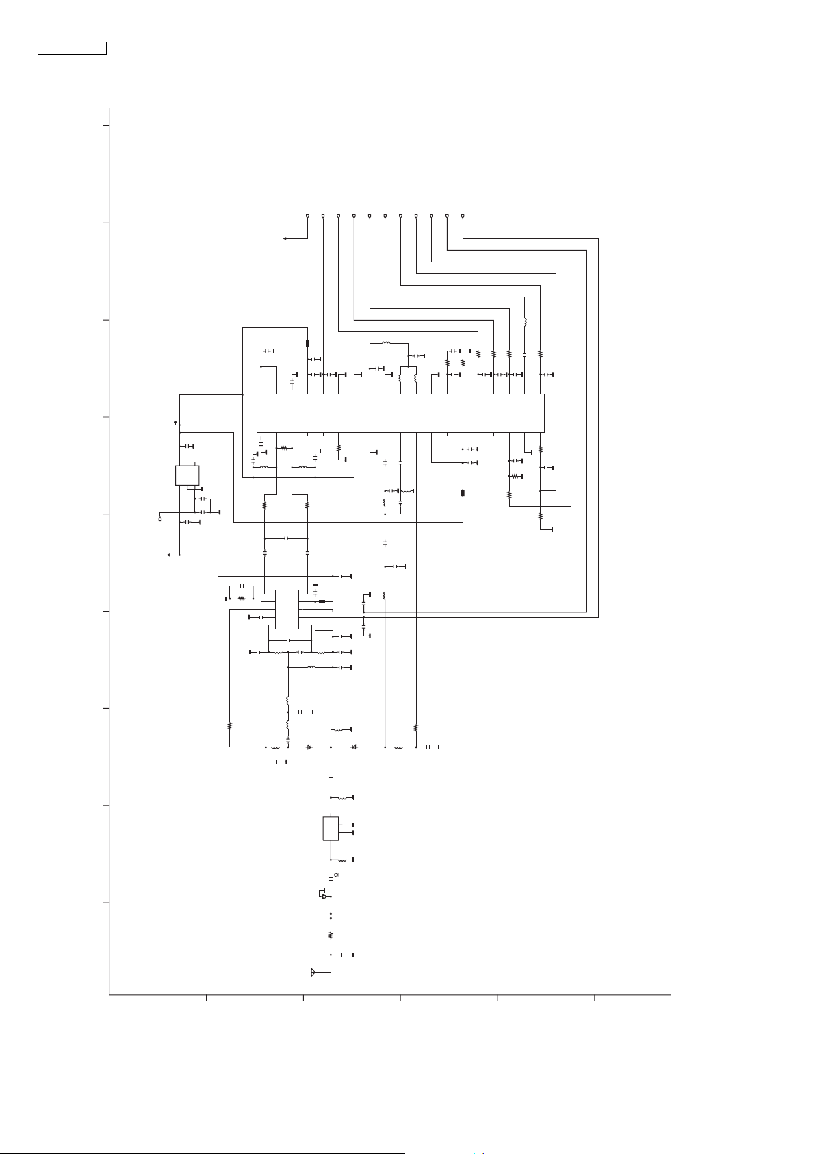
KX-TCA175UK
13.2. Handset (RF Unit)
CK601
1.0u
C677
5
4
NC
VOUT
VIN2VSS3CE
IC603
1
C682
0.01
C681
0.01
RFCONT
C675
1.0u
BATT
C690 8p
R623
560
TXDA
C609 0.01
R603
26PD27
GNDTX
PAON
C608
1000p
2.7k
R604
25
FB603
PSEL
R605
8.2k
C620 C622
12p
24
ICHP
C627
10p
C626
0.01
F.B
SYEN
1k
R606
R607
C621
12p
12p
22
23
SYCL
SYDA
C625
47p
R612
1.2k
R611
3.9k
SYRI
R613
27nH
C634
30
C631
L606
L632
C632
3p
RXDSG
L601
29
VCOK1
GNDREG2
8p
C630
L608
2.7nH
C633
2.7nH
3p
C691
1p
0
4.7nH
8p
3p
C606
8p
L602
28
RSSI
4.7nH
VCOK2
RXDA
BATT
BATT
SHR38SHC
R645
330
C645
0.5p
PIX
PSET
VCCS
PAON
PRAMP
PSEL
POX
NC
C680
VCC
C684
F.B
FB606
C604
0.01
C603
C605
10p
10p
10p
34
35
36PF37
RXDA
VCCRXIF
10p
C672
L603
27nH27nH
10
R634
6p
C643
10p
PI
F.B
5
C647
4
R632
3
2
PO
1
L611
C653
3.3nH
2p
L631
27nH
C601
2200p
IC601
NC12DR3DRX4NC45NC56DIREF7VCCRXRF8GNDRXRF9RF10RFX11RXON12VCC113BPNP14VCCPLL15VCCBG116GNDREG117TXDA18GNDPLL19RSSI
1
10p
C683
L605
C671 10p
10
R633
6p
C642
IC602
6
7
C651
8
9
68p
10
C652
2p
L610
3.3nH
R615
C646
C699
C650
C678
SYEN
33
GNDC
0.1
0.1
8p
10p
3.3k
SYDA
32
GNDRXIF
C649
C648
SYCL
C607
0.01
31
VCC2
10p10p
L630
C610
21
SYRI
12p1k1k
47nH
R608
R610
R614
C623
12p
20
RXDSG
C624
1000p
KX-TCA175UK RF SCHEMATIC DIAGRAM
1k
10k
22k
L614
5.6nH
C656
1.5p
L620 10nH
L615
270
R625
45 7632 8109
B
5.6nH
8p
D601
C657
L616
BAR89-02LRH
27nH
C654
10p
C
FIL601
TP601
JP601
BAR89-02LRH
8p
C665
L621
10nH
4
2
C670
5.6mH
0
C666
12
C673
NC
C674
D602
3
1
D
L617
8.2nH
R626
C660
10p
220
E
F
G
56
Page 57
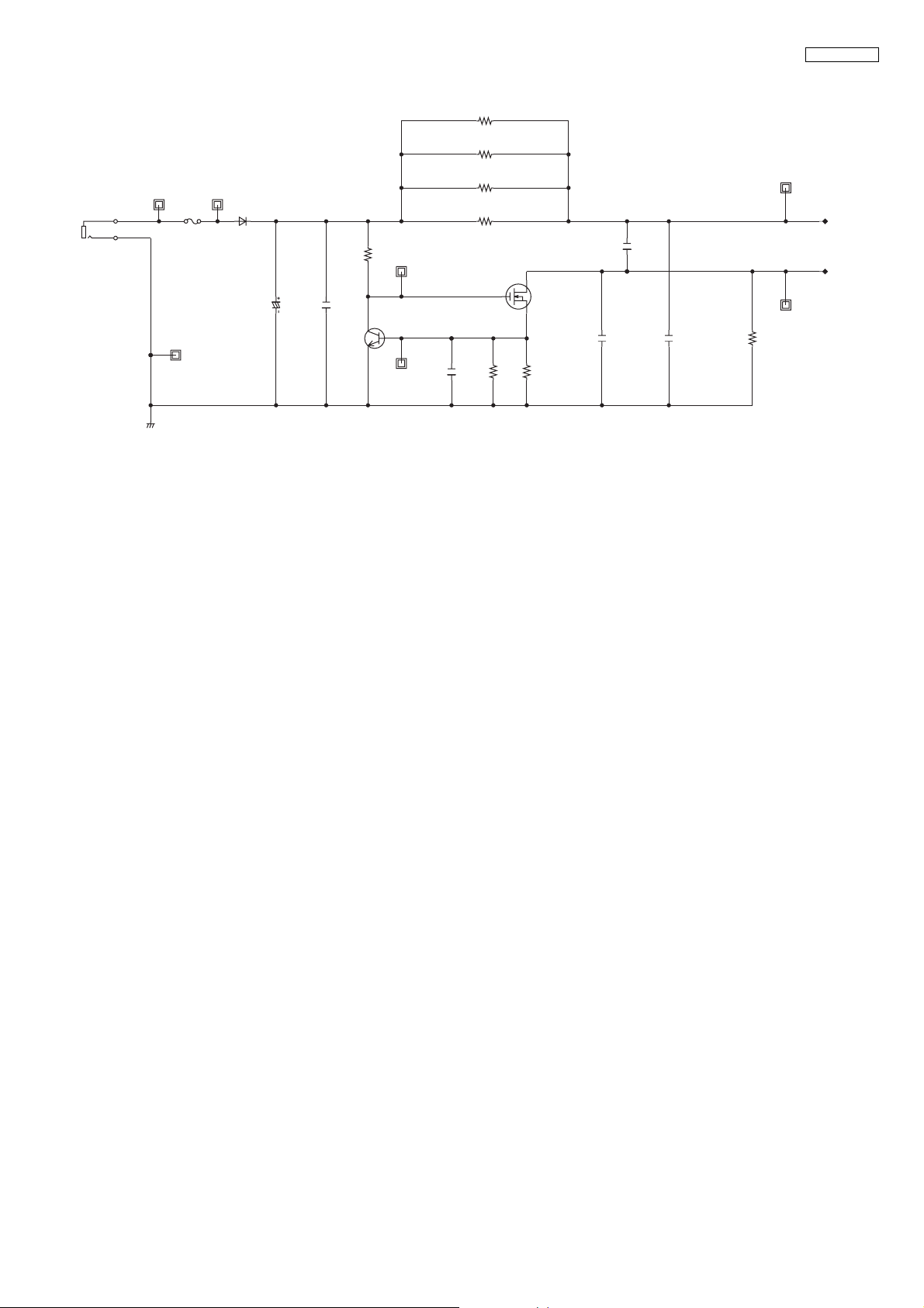
13.3. Charger Unit
CK1 CK3
CN1
1
2
IP1
CK2
D1
C1
NC
C2
NC
R1
NC
Q1
NC
CK4
CK5
C3
NC
R6
NC
R3
R4
R5
R2
22
22
22
NC
KX-TCA175UK
CK6
CHRG+
C5
C4
NC
NC
C6
1500p
R8
CHRG-
CK7
0
Q2
NC
D
G
S
R7
NC
KX-TCA175UK CHARGER UNIT SCHEMATIC DIAGRAM
57
Page 58
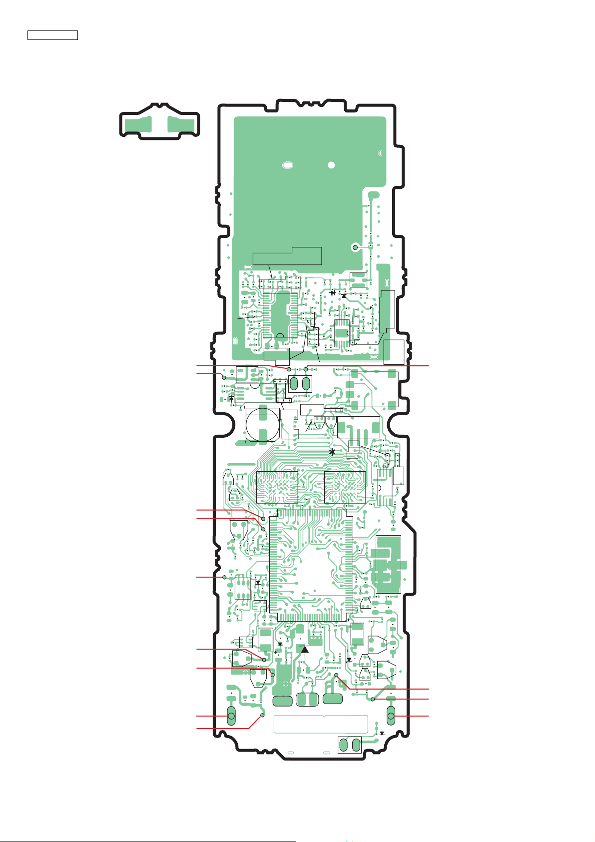
KX-TCA175UK
14 Printed Circuit Board
14.1. Handset
14.1.1. Component View
POS1
C674
C673
CK11
CK601
CK7
CK6
CK10
CK17
CK18
CN4
CN2
R53
C40
C41
R24
R37
R603
C606
L601
C677
1
D25
C44
Q7
L4
R1
C27
R26
L1
C22
C28
C29
C622
R613
C605
FB606
IC603
R3
Q6
Q1
C26
IC4
R29
R75
Q8
R607
C609
L602
C603
C604
IC605
C46
R4
R25
R73
R11
Q17
C5
CHG-
R606
C621
C601
C681
C682
C675
R605
C620
IC601
R615
C632
Br
R67
C60
C54
C49
C683
R41
C53
C48
R614 R611
C624
R610
C67
C73
C56
R58
R608
C623
L630
C608
C684
C610
R604
C607
C630 C633
C631 L606
C108
PSUP1709Z -A
IC2
R86
R8
R6
R9
R18
C9
C10
R31
R39
R30
D16
R36
C72
Q11
R33
R32
R34
C19
R28
R5
Q10
C4
C109
D15
C25
BATT-
C20
R38
C30
C12
R35
R72
R612
C625
FB603
C626
C627
L608
R645
C65
R64
R65
R89
R57
PbF
C1
R87
C8
IC3
C21
D13
C36
C37
R70
MIC
R626
C62
W
SPK
C35
R59
R56
R43
C24
C69
C691
C634
Q14
C58
R69
TP601
C660
L617
C665
D602
L632
L620
C649
R632
C648
C646
C647
C643
C645
IC602
C642
C651
R623
C690
R66
C75
C64
C31
C57
R42
Q13
R60
IC1
R27
R40
C23
C39
C38
R52
C61
IP101
Bk R
L621
FIL601
L616
D601
5
4
3
C74
2
CN5
C68
C63
C59
C2
C11
BATT+
C654
C699
C15
C18
C110
D11
R16
C7
R13
R10
VIB
C666
C657
C678
C656
L631
R71
C55
R55
R21
C13
R88
C16
R23
Q12
R20
Q3
Q4
C6
C670
R625
L614
CN1
C70
C66
R74
C122
R7
C17
L3
C14
Q5
JP601
C650
L615
R62
R63
IC6
C33
R15
Q2
R14
D14
C653
C680L611C652
L610
C672
R634
R633
L605 L603
C671
1
R68
C47C45
X1
R42
R17
L2
CHG+
R54
C52
C51
R61
C34
CK12
C43
C50
R22
R21
CN7
CN1
CN3
A
KX-TCA175UK CIRCUIT BOARD Component View
58
Page 59

14.1.2. Flow Solder Side View
PSUP1709Z -B
PbF
D1
PSUP1709Z -A
C121
C120
RA10RA11
1
R2
C3
RA5 RA4 RA3 RA2
RA9
CN2
KX-TCA175UK
Bk R
RECV
RA7RA8
RA6
RA1
D19
D20
D21
SW01
R78
R79
R80
SW11
SW31
SW21
SW51
SW53
SW03
SW33
SW00
D3
D5
D7
D9
D17
SW10
SW30 SW20
SW50
R44
SW52
R46
SW02
R48
SW12
R50
SW13
R76
R47R45
R49
R51
R77
D4
D6
D8
D10
D18
SW40
SW41
SW42
SW32
SW22
SW23
SW43
SW1
R81
R82
R83
D22
D23
D24
A
KX-TCA175UK CIRCUIT BOARD Bottom View
59
Page 60
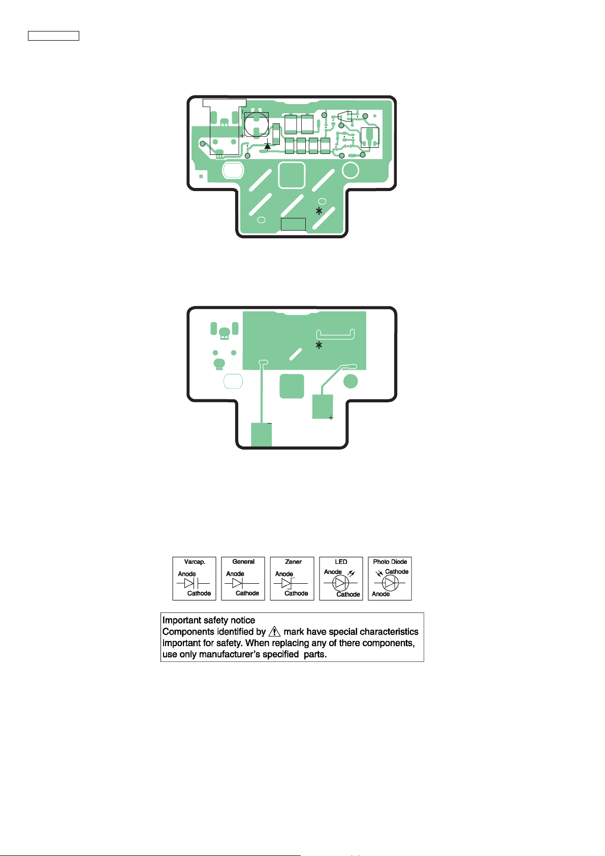
KX-TCA175UK
14.2. Charger Unit
14.2.1. Component View
14.2.2. Flow Solder Side View
CK2
CK1
CN1
C1
IP1
CK3
R6
R7
CK4
D1
C2
R5R4R3R2
PSUP1712Z
PbF
KX-TCA175UK CIRCUIT BOARD
(CHARGER UNIT) Component View
PSUP1712Z
PbF
C3
CK5
Q1
R1
Q2
R8
C4
C5
C6
CK7
CK6
A
CHRG
CHRG
A
KX-TCA175UK CIRCUIT BOARD
(CHARGER UNIT) Bottom View
15 Appendix Information of Schematic Diagram
Note:
1. DC voltage measurements are taken with an oscilloscope or a tester with a ground.
1. The schematic diagrams and circuit board may be modified at any time with the development of new technology.
60
Page 61
16 Exploded View and Replacement Parts List
16.1. CPU Data (Handset)
16.1.1. IC3 (BBIC)
Pin No Description I/O Connection at Normal mode at Reset mode
1 VDDIO - VDDIO - 2VSS - VSS - 3 AD8 D_O AD8 O_0/1 O-0/1
4 AD9 D_O AD9 O_0/1 O-0/1
5 AD10 D_O AD10 O_0/1 O-0/1
6AD11 D_O AD11 O_0/1 O-0/1
7 AD12 D_O AD12 O_0/1 O-0/1
8 AD13 D_O AD13 O_0/1 O-0/1
9 AD14 D_O AD14 O_0/1 O-0/1
10 P3[7]/PD7 D_O RF CONT O_0/1 O-Hi-Z
11 P3[1]/PD1 D_O RXDSG O_0/1 O-Hi-Z
12 P3[5]/PD5 D_O SPAMP O_0/1 O-Hi-Z
13 P3[4]/PD4 D_O LCD_RST O_0/1 O-Hi-Z
14 P3[3]/PD3 D_O PAON O_0/1 O-Hi-Z
15 P3[2]/PD2 D_O PSEL O_0/1 O-Hi-Z
16 VDD - VDD - 17 VSS - VSS - 18 RFCLK D_O SYRI O O-0
19 VDDRF - VDDRF - 20 VSSRF - VSSRF - 21 Xtal1 A_I Xtal1 I I
22 CAP A_I CAP I I
23 AVS - AV S - 24 AVD - AVD - 25 RSSI I RSSI I I
26 RDI D_I RXDA D_I I
27 CMPREF A_I NC D_I D_I
28 TDO A_O TXDA O O
29 AD15 D_O AD15 O_0/1 O-0/1
30 AD16 D_O AD16 O_0/1 O-0/1
31 AD17 D_O AD17 O_0/1 O-0/1
32 AD18 D_O AD18 O_0/1 O-0/1
33 AD19 D_O AD19 O_0/1 O-0/1
34 AD20 D_O AD20 O_0/1 O-0/1
35 AD21 D_O AD21 O_0/1 O-0/1
36 AD22 D_O NC O_0/1 O-0/1
37 AD23 D_O NC O_0/1 O-0/1
38 LE D_O SYEN O_0/1 O-0
39 SO D_O SYDA O_0/1 O-Hi-Z
40 SK D_O SYCL O_0/1 O-0
41 DAC/ADC2 A_I ADC2 A_I I
42 P3[6]/PD6 D_O KEY_BL O_0/1 O-Hi-Z
43 RDN D_O READ O_0/1 O-1
44 WRN D_O WRT O_0/1 O-1
45 MI/READY D_IPU NC I-PU_0/1 I-PU
46 SCLK D_O NC O_0/1 O-1
47 UTX/P0[0] D_O UTX O-PU_0/1 I-PU
48 URX/P0[1] D_I URX I_0/1 I
49 JTIO/P0[2] D_IPU JTIO I-PU_0/1 I-PU
50 PCM_FSC1/P0[3] D_I COL0 I_0/1 I-PU
51 PCM_FSC0/P0[4] D_I COL1 I_0/1 I-PU
52 PCM_CLK/P0[5] D_I COL2 I_0/1 I-PU
53 PCM_DOUT/P0[6] D_I COL3 I_0/1 I-PU
54 PCM_DIN/P0[7] D_I COL4 I_0/1 I-PU
55 VDDIO - VDDIO - 56 VSS - VSS - 57 DREQ0n/INT0n/P1[0] D_O ROW0 O_0/1 I-PU
58 DACK0n/INT1n/P1[1] D_O ROW1 O_0/1 I-PU
59 ACS1/DREQ1n/INT2n/P1[2] D_O SRAM_CS O_0/1 I-PU
60 ACS0 D_O FLASH_CS O_0/1 O-1
61 ACS2/DACK1n/INT3n/P1[3] D_O LCD_CS O_0/1 I-PU
62 HOLDn/INT4n/P1[4] D_O ROW2 O_0/1 I-PU
63 VDDE/HOLDACKn/INT5n/P1[5] D_O ROW3 O_0/1 O-1
64 BE1n D_O SRAM_UB O_0/1 O-1
65 BE0n D_O SRAM_LB O_0/1 O-1
KX-TCA175UK
61
Page 62

KX-TCA175UK
Pin No Description I/O Connection at Normal mode at Reset mode
66 SCL2/P3[0] D_I COL5 I_0/1 O-1
67 SDA2 D_O NC O_0 I
68 DAB0 D_I/O DB0 I/O_0/1 O-1
69 DAB8 D_I/O DB8 I/O_0/1 O-1
70 DAB1 D_I/O DB1 I/O_0/1 O-1
71 DAB9 D_I/O DB9 I/O_0/1 O-1
72 DAB2 D_I/O DB2 I/O_0/1 O-1
73 DAB10 D_I/O SB10 I/O_0/1 O-1
74 DAB3 D_I/O DB3 I/O_0/1 O-1
75 DAB11 D_I/O DB11 I/O_0/1 O-1
76 VSS - VSS - 77 VDD - VDD - 78 VDDIO - VDDIO - 79 P2[0]/PWM0/SPIDI D_O LCD_BL O_0/1 I
80 P2[1]/PWM1/SPICLK D_O RLED O_0/1 I
81 P2[2]/ADC0/CLK100 D_O GLED O_0/1 I
82 P2[3]/ADC1 D_O 5V_CTRL O_0/1 I
83 P2[4]/SCL1 D_O VIB_CTRL O_0/1 I
84 P2[5]/SDA1 D_O RCVAMP O_0/1 I
85 DAB4 D_I/O DAB4 I/O_0/1 O-1
86 DAB12 D_I/O DAB12 I/O_0/1 O-1
87 DAB5 D_I/O DAB5 I/O_0/1 O-1
88 DAB13 D_I/O DAB13 I/O_0/1 O-1
89 DAB6 D_I/O DAB6 I/O_0/1 O-1
90 DAB14 D_I/O DAB14 I/O_0/1 O-1
91 DAB7 D_I/O DAB7 I/O_0/1 O-1
92 DAB15 D_I/O DAB15 I/O_0/1 O-1
93 P2[7]/DC_CTRL/SPIDO D_O NC O_0/1 O-0
94 DC_I A_I GND I I
95 P1[6]/PON/INT6 A_I PON I I-PD(160k pull down)
96 P1[7]/CHARTGE/INT7 A_I CHARGE I I-PD(160k pull down)
97 P2[6]/stop_charge A_O CHARGE_STOP O O-0
98 VBAT3/RINGING A_I VBAT3 I I
99 DC_stab A_O NC O O
100 DC_Sense A_I GND I I
101 AVS_sense A_I GND I I
102 ADC3 A_I CCR+ I I
103 LDO1_Sense A_I LDO1_SNS I I
104 LDO1_CTRL A_O LDO1_CTRL O O-1
105 LDO2_CTRL A_O LDO2_CTRL O O-0
106 VBAT2 A_I VBAT2 I I
107 VBAT1 A_I VBAT1 I I
108 AVS2 - AVS2 - 109 AVD2 - AVD2 - 110 LSR+/REF A_O LSR+ O O
111 LSR-/REF A_O LSR- O O
112 LSR_HS/CIDIN- A_O SP_INPUT O O
113 VREF_HS/CIDOUT A_O NC O O
114 M IC- A _I N C I I
115 V REF - A_O AG ND O O
116 VBUF A_O VBUF O O
117 A GND A_ O AGND O O
118 M IC+ A_ I MI C+ I I
119 VREF+/CIDIN+ A_O MIC_BIAS O I
120 RSTn D_O RSTn O I-PU(80k pull up)
121 AD0/EXT_MEMORY A_I EXT_MEMORY D_IPD I_PD
122 AD1 D_O A0 O_0/1 O-0/1
123 AD2 D_O A1 O_0/1 O-0/1
124 AD3 D_O A2 O_0/1 O-0/1
125 AD4 D_O A3 O_0/1 O-0/1
126 AD5 D_O A4 O_0/1 O-0/1
127 AD6 D_O A5 O_0/1 O-0/1
128 AD7 D_O A6 O_0/1 O-0/1
62
Page 63
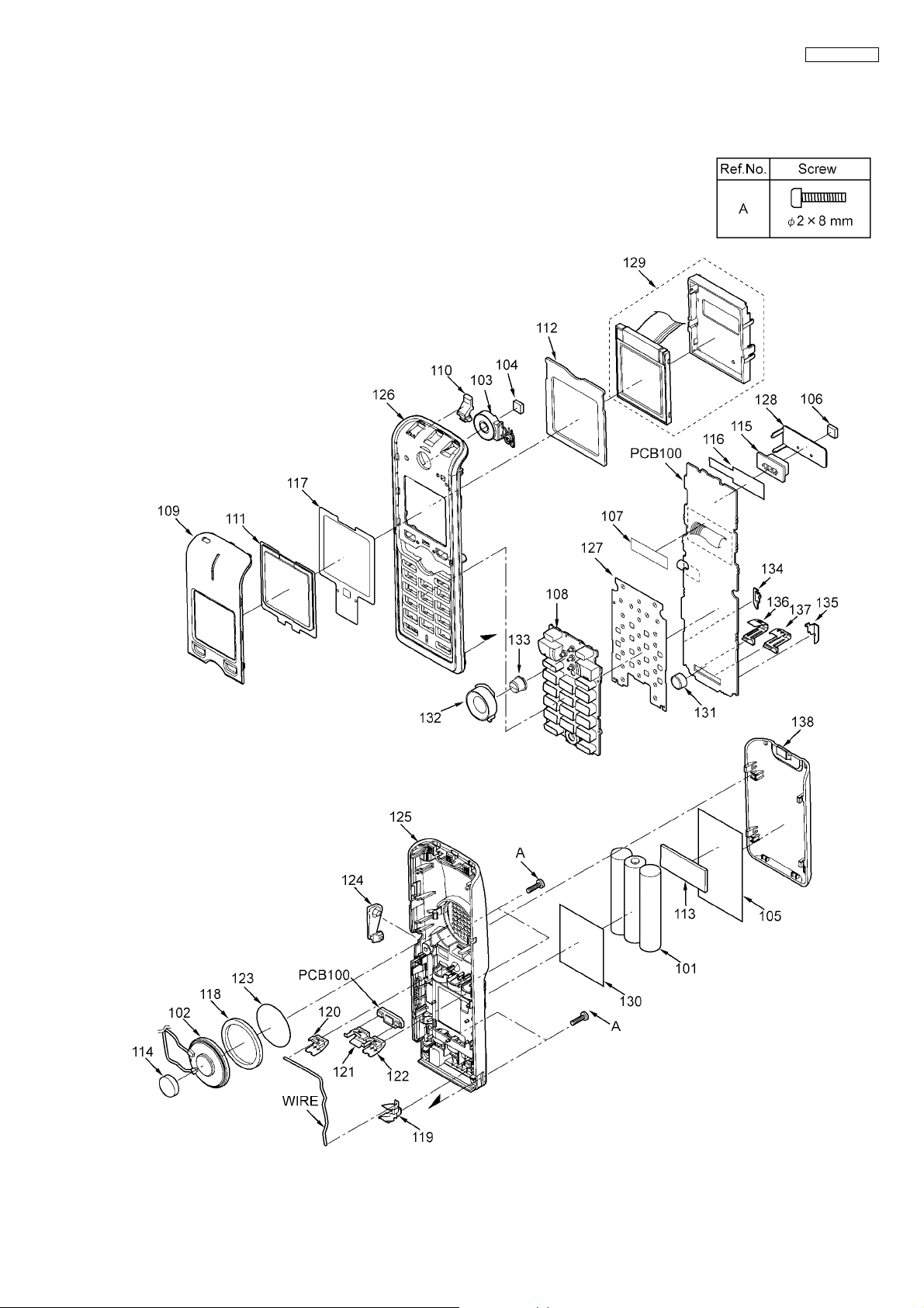
16.2. Cabinet and electrical Parts Location
16.2.1. Handset
KX-TCA175UK
63
Page 64

KX-TCA175UK
16.2.2. Charger Unit
64
Page 65
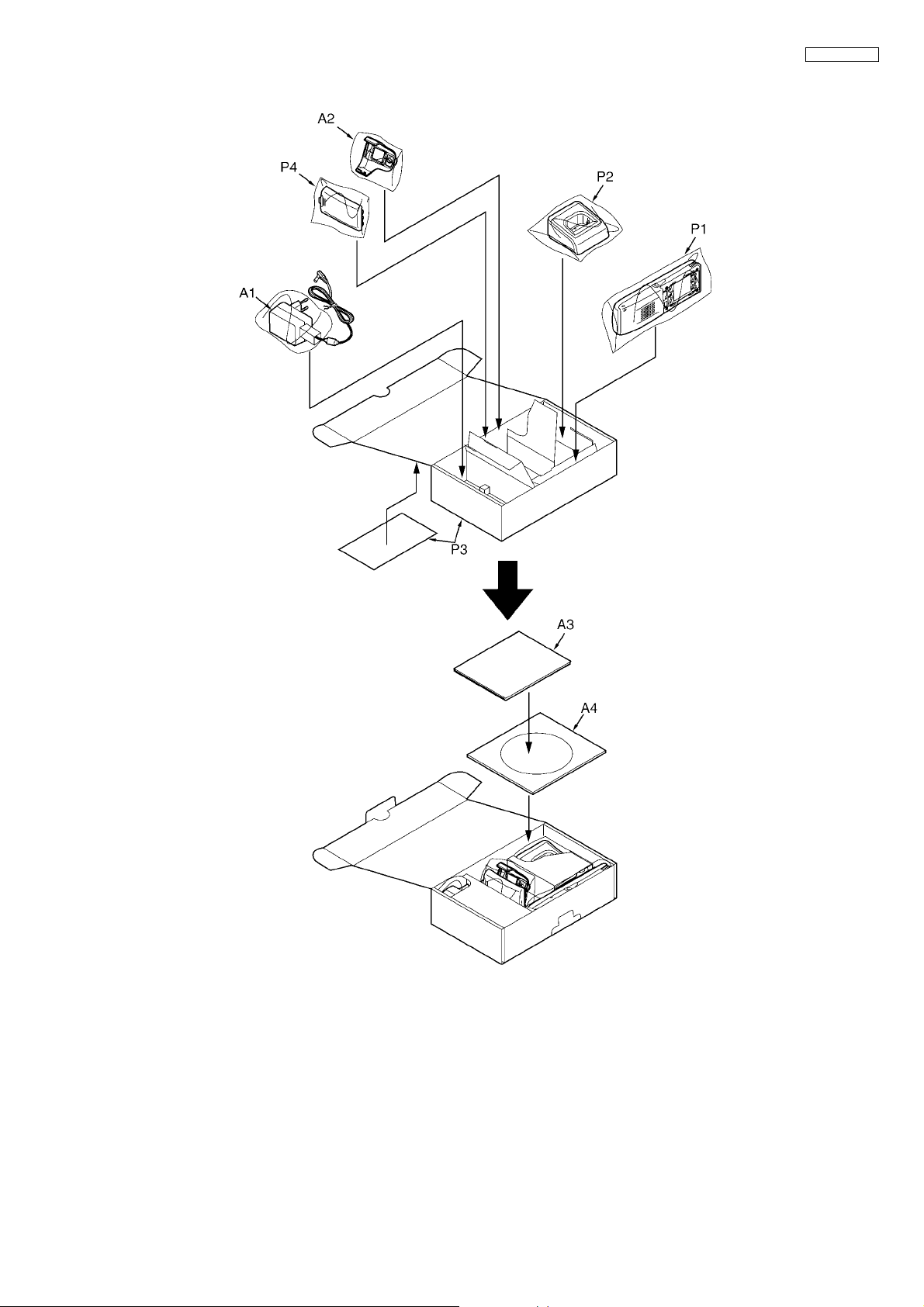
16.2.3. Accessories and Packing Materials
KX-TCA175UK
65
Page 66

KX-TCA175UK
16.3. Replacement Parts List
Note:
1. RTL (Retention Time Limited)
The "RTL" marking indicates that its Retention Time is
Limited.
When production is discontinued, this item will continue to
be available only for a specific period of time.
This period of time depends on the type of item, and the
local laws governing parts and product retention.
At the end of this period, the item will no longer be available.
2. Important safety notice
Components identified by the mark indicates special
characteristics important for safety. When replacing any
of these components, only use specified manufacture's
parts.
3. The S mark means the part is one of some identical parts.
For that reason, it may be different from the installed part.
4. ISO code (Example: ABS-94HB) of the remarks column
shows quality of the material and a flame resisting grade
about plastics.
5. RESISTORS & CAPACITORS
Unless otherwise specified;
All resistors are in ohms (Ω), k=1000Ω, M=1000kΩ
All capacitors are in MICRO FARADS (µF), p=µµF
*Type & Wattage of Resistor
Safety Ref.
No.
115 PSHR1357Z SPACER,ANTENNA ABS-HB
116 PSHS1081Z TAPE,BOTH SIDE
117 PSHS1086Z TAPE,BOTH SIDE
118 PSHS1052Z NET,SPEAKER
119 PSJC1014Z BATTERY TERMINAL (B_+)
120 PSJC1015Z BATTERY TERMINAL (B_-)
121 PSJC1018Z BATTERY TERMINAL (C_3A)
122 PSJC1019Z BATTERY TERMINAL (C_3B)
123 PQHG10666Z SPACER ,SP RUBBER SHEET
124 PSKE1105Z1 CAP,EARPHONE
125 PSYF1079Z1 CABINET COVER ABS-HB
126 PSKM1180Z1 CABINET BODY ABS-HB
127 PSSE1028Z SPECIAL SWITCH,SHEET
128 PSUL1011Z METAL PARTS,PLATE
129 PSWECA275CER LCD ASS'Y
130 PSYE175UKRV7 NAME PLATE
130 PSYE175UKRV4 NAME PLATE
131 L0CBAB000104 MICROPHONE
132 PSBC1072Y2 CURSOR KEY
133 PSBC1073Y2 CENTER KEY
134 PSJT1058Z CHARGER TERMINAL (A)
135 PSJT1059Z CHARGER TERMINAL (B)
136 PSJC1012Z BATTERY TERMINAL (A_+)
137 PSJC1013Z BATTERY TERMINAL (A_-)
138 PSKK1066Z1 COVER, BATTERY ABS-HB
A XTB2+8GFJ
Part No. Part Name & Description Remarks
(LCD GRILLE)
ANTENNA
(Marked by V7)
(Marked by V4)
SCREW
16.3.2. Cabinet and Electrical Parts
(Charger unit)
16.3.1. Cabinet and Electrical Parts (Handset)
Safety Ref.
No.
101 HHR-4EPT/GPE BATTERY
102 L0AD02A00010 SPEAKER
103 L0AD01A00017 S P EA KE R
104 PQHA10023Z RUBBER PARTS,FOOT
105 PNMY1016Z SPACER,SHEET
106 PQHA10023Z RUBBER PARTS,FOOT
107 PQHS10608Z T AP E
108 PSSX1051Z2 PUSH BUTTON,KEY TOP ASSY
109 PSGG1030Z2 G R I L L E , L C D A B S - H B
110 PSGP1158Z1 COVER,LED LENS ABS-HB
111 PSGP1159Z P A N E L , L C D P M M A - H B
112 PSHE1222Z SPACER,LCD SPONGE
113 PSHE1223Y SPACER,BATTERY CUSHION
114 PSHG1297Z SPEAKER,RUBBER SPACER
Part No. Part Name & Description Remarks
Safety Ref.
No.
1 PSWEA175UKV7 HANDESET CHARGER
1 PSWEA175UKV4 HANDESET CHARGER
1-1 PQHA10023Z RUBBER PARTS,FOOT
1-2 PSJT1061Z TERMINAL,CHARGE TERMI-
1-3 PSKF1144Z1 CABINET COVER PS-HB
1-4 PSKM1181Z1 CABINET BODY PS-HB
1-5 PSYE175UKHV7 NAME PLATE
1-5 PSYE175UKHV4 NAME PLATE
B PQHV2612PJ65 SCREW
16.3.3.
Part No. Part Name & Description Remarks
(Marked by V7)
(Marked by V4)
NAL SPRING
(Marked by V7)
(Marked by V4)
Accessories and Packing
Materials
Safety Ref.
No.
A1 PQLV219EY AC ADAPTOR
A2 PSKE1107Z1 COVER,BELT CLIP POM-HB
A3 PSQX4979Z INSTRUCTION BOOK,QUICK
A4 PNQC1022Y CD-ROM,INSTRUCTION BOOK
P1 PQPP10084Z PROTECTION COVER
P2 PQPP10086Z PROTECTION COVER
P3 PSZKA175UKV7 GIFT BOX (Marked by V7)
P3 PSZKA175UKV4 GIFT BOX (Marked by V4)
P4 PQPP10102Z PROTECTION COVER
Part No. Part Name & Description Remarks
GUIDE
(for Handset)
(for Charger)
66
Page 67
16.3.4. Handset Board Parts
Safety Ref.
No.
PCB100 PSLP1611Z MAIN P.C.BOARD ASS'Y
IC1 C3BBJG000031 I C
IC2 It is impossible to replace IC2 by
IC3 C1CB00001830 I C
IC4 C0DBZHA00012 I C
IC601 C1CB00001690 I C
IC602 C1CB00001691 I C
IC603 C0CBCBC00171 I C
IC605 C1BB00000265 I C
Q1 B1ABGE000006 TRANSISTOR(SI)
Q2 B1ADGE000004 TRANSISTOR(SI)
Q3 PSVTDTC143X TRANSISTOR(SI) S
Q4 B1ABCF000103 TRANSISTOR(SI)
Q6 B1GBCFYY0034 TRANSISTOR(SI) S
Q7 B1GBCFYY0034 TRANSISTOR(SI) S
Q8 B1ADGE000004 TRANSISTOR(SI)
Q10 B1ADGE000004 TRANSISTOR(SI)
Q11 XP0421600L TRANSISTOR(SI)
Q12 B1GBCFGA0001 TRANSISTOR(SI) S
Q13 B1ABCF000103 TRANSISTOR(SI)
Q14 B1ABCF000103 TRANSISTOR(SI)
Q17 XP0431600L TRANSISTOR(SI)
D1 B3AGB0000050 D I O D E ( S I )
D3 LNJ308G8JRA LED
D4 LNJ308G8JRA LED
D5 LNJ308G8JRA LED
D6 LNJ308G8JRA LED
D7 LNJ308G8JRA LED
D8 LNJ308G8JRA LED
D9 LNJ308G8JRA LED
D10 LNJ308G8JRA LED
D11 PSVDUDZ20B D I O D E ( S I ) S
D13 B0JCME000038 D I O D E ( S I )
D15 MA2Z72000 D I O D E ( S I )
D16 B0JCDD000002 D I O D E ( S I )
D17 LNJ308G8JRA LED
D18 LNJ308G8JRA LED
D19 LNJ308G8JRA LED
D20 LNJ308G8JRA LED
D21 LNJ308G8JRA LED
D22 LNJ308G8JRA LED
D23 LNJ308G8JRA LED
D24 LNJ308G8JRA LED
D25 B0JCDD000002 LED
D601 B0DCCJ000002 D I O D E ( S I )
D602 B0DCCJ000002 D I O D E ( S I )
L1 G1C100MA0072 C OI L
L2 G1C100MA0072 C OI L
L3 G1C4R7M00012 C OI L
L4 PQLQR2KA12T C O I L S
L601 G1C4N7Z00017 C OI L
L602 G1C4N7Z00017 C OI L
L603 PSLQR1S27NJ C O I L
L605 PSLQR1S27NJ C O I L
L606 PQLQR4C2N7S C O I L S
L608 PQLQR4C2N7S C O I L S
L610 G1C3N3ZA0061 C OI L
L611 G1C3N3ZA0061 C OI L
L614 PQLQR4C5N6S C O I L S
L615 PQLQR4C5N6S C O I L S
Part No. Part Name & Description Remarks
(RTL)
(ICs)
itself. To replace IC102 replace the
PCB1assembly.
(TRANSISTORS)
(DIODES)
(COILS)
Safety Ref.
No.
L616 PSLQR1S27NJ C O I L
L617 G1C8N2J00004 C OI L
L620 PQLQR4C10NJ C O I L S
L621 PQLQR4C10NJ C O I L S
L630 G1C47NJ00010 C OI L
L631 PSLQR1S27NJ C O I L
C670 PQLQR4C5N6S C O I L S
R613 PSLQR1S1N0S C O I L
RA1 D1H8R0040009 RESISTOR ARRAY, 0
RA2 D1H8R0040009 RESISTOR ARRAY, 0
RA3 D1H8R0040009 RESISTOR ARRAY, 0
RA4 D1H8R0040009 RESISTOR ARRAY, 0
RA5 D1H8R0040009 RESISTOR ARRAY, 0
RA6 F5A84100A015
RA7 F5A84100A015
RA8 F5A84100A015
RA9 F5A84100A015
RA10 F5A84100A015
RA11 F5A84100A015
CN2 K1MN32BA0070 CONNECTOR, 32P
CN5 K1KA03AA0083 CONNECTOR, 3P
X1 H0J103500024 CRYSTAL OSCILLATOR S
FB603 J0JBC0000043 IC FILTER
FB606 J0JBC0000043 IC FILTER
FIL601 J0D1890B0002 CERAMIC FILTER
R632 J0JBC0000043 IC FILTER
IP101 K5H312200002 F U S E
CN1 K2HD103D0001 JACK
POS1 D4FB1R500010 THERMISTOR
C1 ECJ0EF1C104Z 0.1
C2 ECJ0EF1C104Z 0.1
C3 ECJ0EF1C104Z 0.1
C4 F1G1A4740003 0.47
C5 ECJ1VF1A105Z 1
C6 ECJ0EB1A473K 0.047
C7 ECJ0EF1C104Z 0.1
C8 ECJ0EF1C104Z 0.1
C9 ECJ0EF1C104Z 0.1
C10 ECJ0EF1C104Z 0.1
C11 ECJ0EF1C104Z 0.1
C12 ECJ0EF1C104Z 0.1
C13 ECJ0EC1H040C 4 p
C14 ECUE1H330JCQ 3 3p S
C15 ECJ0EF1C104Z 0.1
C16 F1G1A4740003 0.47
C17 ECUE1H120JCQ 1 2p S
C18 ECJ0EF1C104Z 0.1
C19 F1G1A2240008 0.22
C20 ECJ0EF1C104Z 0.1
C21 ECJ0EB1A683K 0.068
C22 ECJ0EF1C104Z 0.1
C23 F1G1H100A420 10p S
C24 ECJ0EB1A683K 0.068
C25 F1J0J2260002 22
C26 ECJ0EB1H102K 0.001
C27 ECJ1VF1A105Z 1
C28 ECJ1VF1A105Z 1
Part No. Part Name & Description Remarks
(COMPONENTS PARTS)
(CONNECTORS)
(CRYSTAL OSCILLATOR)
(FILTERS)
(FUSE)
(JACK)
(THERMISTOR)
(CAPACITORS)
KX-TCA175UK
67
Page 68

KX-TCA175UK
Safety Ref.
No.
C29 ECJ0EF0J105Z 1
C33 F1J0J2260002 22
C34 F1J0J2260002 22
C35 ECJ1VB1C104K 0.1
C36 F1G1H100A420 10p S
C37 F1J0J2260002 22
C38 ECJ1VB1C104K 0.1
C39 F1G1H100A420 10p S
C40 ECJ0EF1C104Z 0.1
C41 ECJ1VB0J105K 1
C42 F1G1H100A420 10p S
C44 ECUE1H470JCQ 4 7p S
C46 F1G1H100A420 10p S
C48 ECUE1H471KBQ 4 70 p S
C49 F1G1H100A420 10p S
C53 F1G1H100A420 10p S
C54 ECJ0EF1C104Z 0.1
C56 F1G1H100A420 10p S
C57 F1G1H100A420 10p S
C58 F1G1H100A420 10p S
C60 F1G1H100A420 10p S
C61 EZAEG2A50AX ESD
C62 ECJ0EC1H050C 5 p
C64 F1G1H100A420 10p S
C65 F1G1H100A420 10p S
C67 F1G1H100A420 10p S
C68 F1G1H100A420 10p S
C69 F1G1H100A420 10p S
C70 ECJ0EB1H272K 0.0027 S
C72 ECJ0EF1C104Z 0.1
C73 ECJ0EC1H050C 5 p
C74 ECJ0EB1H102K 0.001 S
C75 ECJ0EB1H102K 0.001
C108 EEE0JA221WP 220 S
C109 F3K0J107A002 100
C110 F3K0J107A002 100
C120 ECJ0EF1C104Z 0.1
C121 ECJ0EF1C104Z 0.1
C122 F1G1H100A420 10p S
C601 F1J1H2220008 0.0022
C603 F1G1H100A420 10p S
C604 ECJ0EB1C103K 0.01
C605 F1G1H100A420 10p S
C606 ECUE1H1R5CCQ 1.5 S
C607 ECJ0EB1C103K 0.01
C608 ECJ1VC1H102J 0.001
C609 ECHU1C103GB 0.01
C610 ECUE1H120JCQ 1 2p S
C620 ECUE1H120JCQ 1 2p S
C621 ECUE1H120JCQ 1 2p S
C622 ECUE1H120JCQ 1 2p S
C623 ECUE1H120JCQ 1 2p S
C624 ECJ0EB1H102K 0.001
C625 ECUE1H470JCQ 4 7p S
C626 ECJ0EB1C103K 0.01
C627 F1G1H100A420 10p S
C630 ECJ0EC1H080D 8 p
C631 ECJ0EC1H080D 8 p
C632 ECUE1H030CCQ 3 p S
C633 ECUE1H030CCQ 3 p S
C634 ECUE1H030CCQ 3 p S
C642 ECJ0EC1H060C 6 p S
C643 ECJ0EC1H060C 6 p S
C645 ECJ0EC1H0R5B 0.5
C646 ECJ0EB1A104K 0.1
C647 F1G1H100A420 10p S
C648 F1G1H100A420 10p S
C649 F1G1H100A420 10p S
C650 ECJ0EC1H080D 8 p
C651 ECUE1H680JCQ 6 8p S
C652 ECUE1H020CCQ 2 p S
C653 ECUE1H020CCQ 2 p S
C654 F1G1H100A420 10p S
Part No. Part Name & Description Remarks
Safety Ref.
No.
C656 ECUE1H1R5CCQ 1.5 S
C657 ECJ0EC1H080D 8 p
C660 F1G1H100A420 10p S
C665 ECJ0EC1H080D 8 p
C666 ERJ2GE0R00 0
C671 F1G1H100A420 10p S
C672 F1G1H100A420 10p S
C673 ERJ2GE0R00 0
C675 ECJ1VB0J105K 1
C677 ECJ1VB0J105K 1
C678 F1G1H100A420 10p S
C681 ECJ0EB1C103K 0.01
C682 ECJ0EB1C103K 0.01
C683 F1G1H100A420 10p S
C684 F1G1H100A420 10p S
C690 ECJ0EC1H080D 8 p
C691 ECUE1H010CCQ 1 p S
C699 ECJ0EB1A104K 0.1
L632 ERJ2GE0R00 0
R1 PQ4R10XJ101 100 S
R2 ERJ2GE0R00 0
R3 ERJ2GEJ104 100k
R4 ERJ2GEJ104 100k
R5 ERJ6RQJR22 0.22
R6 ERJ2GEJ103 10k
R7 ERJ2GEJ102 1 k
R8 ERJ2GEJ102 1 k
R9 ERJ2GEJ102 1 k
R10 ERJ2GEJ564 560k
R11 ERJ2GEJ103 10k
R12 ERJ2GEJ103 10k
R14 ERJ2GEJ103 10k
R15 ERJ2GEJ471 470
R16 ERJ2GEJ102 1 k
R18 ERJ2GEJ393X 39k
R23 ERJ2GE0R00 0
R24 ERJ2GEYJ121 120 S
R25 ERJ2GEJ330 33
R26 ERJ2GEJ153 15k
R27 ERJ2GEJ103 10k
R28 ERJ2GEJ562 5.6k
R30 ERJ2GEJ683 68k
R31 ERJ2GEJ683 68k
R32 ERJ3EKF4302V 43k
R33 ERJ3EKF1802V 18k
R34 ERJ2GEJ105X 1M
R35 ERJ2GEYJ274 270k S
R36 ERJ2GEJ104 100k
R37 ERJ2GEJ103 10k
R38 ERJ2GEJ474X 470k
R39 ERJ2GEJ104 100k
R40 ERJ2GEJ331 330
R41 ERJ2GEJ273X 27k
R42 ERJ2GE0R00 0
R43 ERJ2GEJ101 100
R44 ERJ2GEYJ121 120 S
R45 ERJ2GEYJ121 120 S
R46 ERJ2GEYJ121 120 S
R47 ERJ2GEYJ121 120 S
R48 ERJ2GEYJ121 120 S
R49 ERJ2GEYJ121 120 S
R50 ERJ2GEYJ121 120 S
R51 ERJ2GEYJ121 120 S
R52 ERJ2GEJ222 2.2k
R53 ERJ2GEJ103 10k
R55 ERJ2GEJ103 10k
R56 ERJ2GEYJ121 120 S
R57 ERJ2GEJ104 100k
R58 ERJ2GEJ683 68k
R59 ERJ2GEJ473 47k
R60 ERJ2GEJ563 56k
Part No. Part Name & Description Remarks
(RESISTORS)
68
Page 69
Safety Ref.
No.
R62 ERJ2GEJ1R0X 1
R63 ERJ2GEJ1R0X 1
R64 ERJ2GEJ473 4 7 k
R65 ERJ2GEJ823 8 2 k
R67 ERJ2GE0R00 0
R69 ERJ2GEJ330 33
R70 ERJ2GEJ330 33
R72 ERJ2GE0R00 0
R73 ERJ2GEJ102 1 k
R74 ERJ2GEJ103 1 0 k
R75 ERJ2GEJ103 1 0 k
R76 ERJ2GEYJ121 120 S
R77 ERJ2GEYJ121 120 S
R78 ERJ2GEYJ121 120 S
R79 ERJ2GEYJ121 120 S
R80 ERJ2GEYJ121 120 S
R81 ERJ2GEYJ121 120 S
R82 ERJ2GEYJ121 120 S
R83 ERJ2GEYJ121 120 S
R88 ERJ2GEJ335X 3.3M
R89 ERJ2GEJ223X 2 2 k
R603 ERJ2GEJ272 2 .7 k
R604 ERJ2GEJ822X 8 . 2 k
R605 ERJ2GEJ102 1 k
R606 ERJ2GEJ102 1 k
R607 ERJ2GEJ102 1 k
R608 ERJ2GEJ102 1 k
R610 ERJ2GEJ103 1 0 k
R611 ERJ2GEYF392 3 . 9 k S
R612 ERJ2GEJ122 1 .2 k
R614 ERJ2GEJ223X 2 2 k
R615 ERJ2GEJ332 3 .3 k
R623 ERJ2GEJ561 560
R625 ERJ2GEJ271 270
R626 ERJ2GEJ221 220
R633 ERJ2GEJ100 10
R634 ERJ2GEJ100 10
R645 ERJ2GEJ331 330
Part No. Part Name & Description Remarks
KX-TCA175UK
16.3.5. Charger unit Board Parts
Safety Ref.
No.
PCB200 PSWPCA175CEH CHARGER P.C.BOARD ASS'Y
D1 MA738 D I O D E ( S I ) S
IP1 K5H311200001 F US E
CN1 K2ECYB000001 JACK
C6 ECUV1H152KBV 0.0015 S
R2 ERJ14YJ220 22
R3 ERJ14YJ220 22
R4 ERJ14YJ220 22
R8 ERJ6GEY0R00 0
Part No. Part Name & Description Remarks
(RTL)
(DIODE)
(FUSE)
(JACK)
(CAPACITOR)
(RESISTORS)
16.3.6. Fixtures and Tools
Safety Ref.
No.
EC1 PSZZ2CA155EU PC CABLE
Part No. Part Name & Description Remarks
NK
KXTCA175UK
69
 Loading...