

Page 1
Panasonic Service and Technology Company
Technical Guide
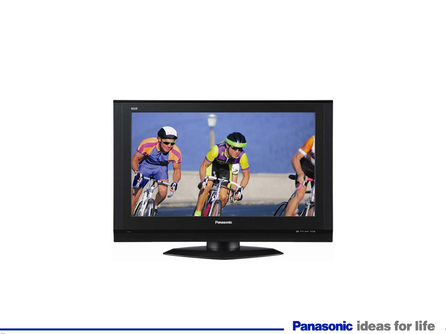
TC-32LX70/700, TC37LZ85, and TC-32LX85 LCD Display Television
National Training
Page 2
Prepared by
Jean Magloire
Panasonic Service and Technology Company
National Training
Copyright © 2008 by Panasonic Services Company
All rights reserved. Unauthorized copying and distribution is a violation of law.
Warning
This service information is designed fo r experienced repair technic ians only and is not designed for use by the general public. It does
not contain warnings or cautions to advise non-technical individuals of potential dangers in attempting to servic e a product. Products
powered by electricity should be serviced or repaired only by experienced pro fessional technicians. Any attempt to service o r repair
the product or products dealt with in this service information by anyone else could result in serious injury or death.
Page 3
Table of Contents
Subject Page # Subject Page #
Topics 5 Self-Check Menu 38
2007 LCD TV Specifications 7 Check Point 39
P.C.B Layout (LX700) 8 Serviceman Mode 40
P.C.B Layout (LX70) 9 Serviceman Mode Menu and Navigation 41
P.C.B Layout (LX700 Pictorial) 10 Adjustment Data 42
P.C.B Layout (LX700 Connectors) 11 SRV-TOOL 43
P.C.B Layout (LX700 LVDS Connector) 12 Voltage chart of AP-board 45
TC-32LX700 Board Description 13 Voltage chart of P and A boards 46
P Board – Main Power Board 15 Voltage chart of DT board 47
Main MPU (Power On Commands) 17 Troubleshooting Signal Problems 49
Standby Operation 19 Picture NG and Sound OK (LX700/LX70 ) 50
SUB Voltages and Over-voltage Protection 21 Picture OK and Sound NG (LX700/LX70) 51
Main Voltages and Over-voltage Protection 22 Picture NG and Sound NG (LX700/LX70 ) 52
Inverter_On Command and Protection 23 No Picture from TV Reception 53
Video Process Block Diagram 25 No Picture 54
Audio Process Block Diagram 27 No Video, Dark Blue Screen 55
MPU SOS Inputs and Blink Codes 29 No Audio 57
Over-Current Protection Circuit 31 No Power 58
Over-Current Protection Circuit 2 33 Power LED Blinks One Time (INV_SOS) 60
Power LED Timing Table 35 Power LED Blinks Three Times (TV_SOS) 61
Self-Check and Reset Function 37 Power LED Blinks Four Times 62
3
Page 4
Table of Contents
Purposely Left Blank
2008 LCD Television Models 63
Full HD TC-LZ85 & HD TC-LX85 Series 64
Chassis structure (37 Full HD type) 65
Chassis structure (37 HD type) 66
Signal Circuit Block Diagram 67
TC-32LX85 / TC37LZ85 Signal Circuit Block Diagram 68
TC37LZ85 Signal Circuit Block Diagram 69
TC32LX85 Signal Circuit Block Diagram 71
TC37LZ85 Audio Circuit Block Diagram 73
TC32LX85 Audio Circuit Block Diagram 75
Power Supply Overview 77
Power Supply Description 78
Self-Check and Reset Function 80
SOS and Power LED Indication 81
Power LED Blinks 6 or 7 Times 85
Power LED Blinks 8 or 9 Times 86
Power LED Blinks 1 Time (TC-32LX85) 87
Power LED Blinks 3 Times (TC-32LX85) 88
Power LED Blinks 4 or 5 Times (TC-32LX85) 89
Power LED Blinks 6 or 7 Times (TC-32LX85) 90
Power LED Blinks 8 or 9 Times (TC-32LX85) 91
Picture Defect) 92
Sound Defect 104
Service Information for 2008 models 105
Internal Pattern generator 106
Copy from the TV to the SD Card 109
Copy Data from the SD Card to the TV 115
Copy Self Check Data to the SD Card 117
Power LED Blinks 1 Time 82
Power LED Blinks 3 Times 83
Power LED Blinks 4 or 5 Times 84
Local maintenance 120
Picture Refresh Mode 128
4
Page 5

Topics
1. Models Comparison
2. Boards Layout
3. Power supply/Standby/Power on
4. Troubleshooting
5. SOS Circuit
6. Video/Audio Processing Circuit
7. Panel Drive Circuit
8. Service Man Mode
9. Self-Check
10.Reset
11.Adjustments
12.Service Information for 2008 models
5
Page 6

Purposely Left Blank
Purposely left blank
6
Page 7
2007 LCD TV Specifications
VIDEO
Screen Size Diagonal (inches) 32 32
Aspect Ratio 16:9 16:9
Number of Pixels 1,049,088 (1,366 x 768) 1,049,088 (1,366 x 768)
Brightness (Panel Luminance) 500 cd/m2 500 cd/m2
Display Capability (1080p, 1080i, 720p, 480P) Y Y
Motion Picture Pro Y —
AUDIO
Speakers Slim squawker x 2, woofer x 2 (L, R) Full-range x 2 (L, R)
Audio Output 20 W (10% THD) 20 W (10% THD)
JACKS
TC-32LX700 TC-32LX70
Integrated ATSC Tuner Y Y
SD Memory Card Slot Y (SDHC Compatible) —
HDMI Input 2 2
Composite Video Input 3 (1 side) 3 (1 side)
S-Video Input 2 2
Component Video Input (Y, P
Monitor Output 1 1
Digital Audio Output 1 1
Headphone Jack 1 1
, PR ) 1 1
B
7
Page 8
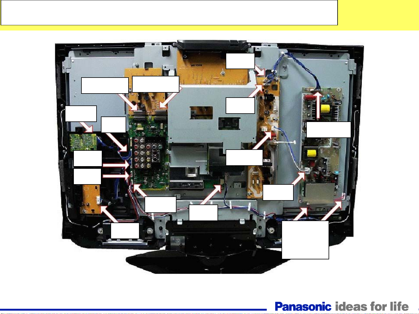
P.C.B Layout (LX700)
P.C.B Layout (LX700)
SP
G
SP
32/26LX600
KEY Control
AP
A
DT
(HDMI)
SP
P
V
SP
32LX700
SP
A
GS
G
SP
KEY Control
INV
AP
SP
P
DT
(HDMI)
SP
V
Differences from LX600:
GS board for SD card slot is added.
The inverter PCB of the LX700 is visible.
8
Page 9
P.C.B Layout (LX70)
P.C.B Layout (LX70)
G
32/26LX60
KEY Control
A
(HDMI)
SP
AP
DT
P
SP
V
G
32/26LX70
KEY Control
AP
A
(HDMI)
SP
DT
P
SP
V
Differences from LX60:
Board structure is almost same.
9
Page 10
P.C.B Layout (LX700 Pictorial)
P.C.B Layout (LX700 Pictorial)
GS Board
Key Control
A Board
AP Board
DT BoardG Board
10
P Board
V Board
Inverter PCB
Page 11
P.C.B Layout (LX700 Connectors)
P.C.B Layout (LX700 Connectors)
P5
GS8
A8
A5
AP3/A3
A7
G4
AP4/A4
P6
CN501
P3
CN1
A6
A9
To
Panel
CCFLTs
11
Page 12
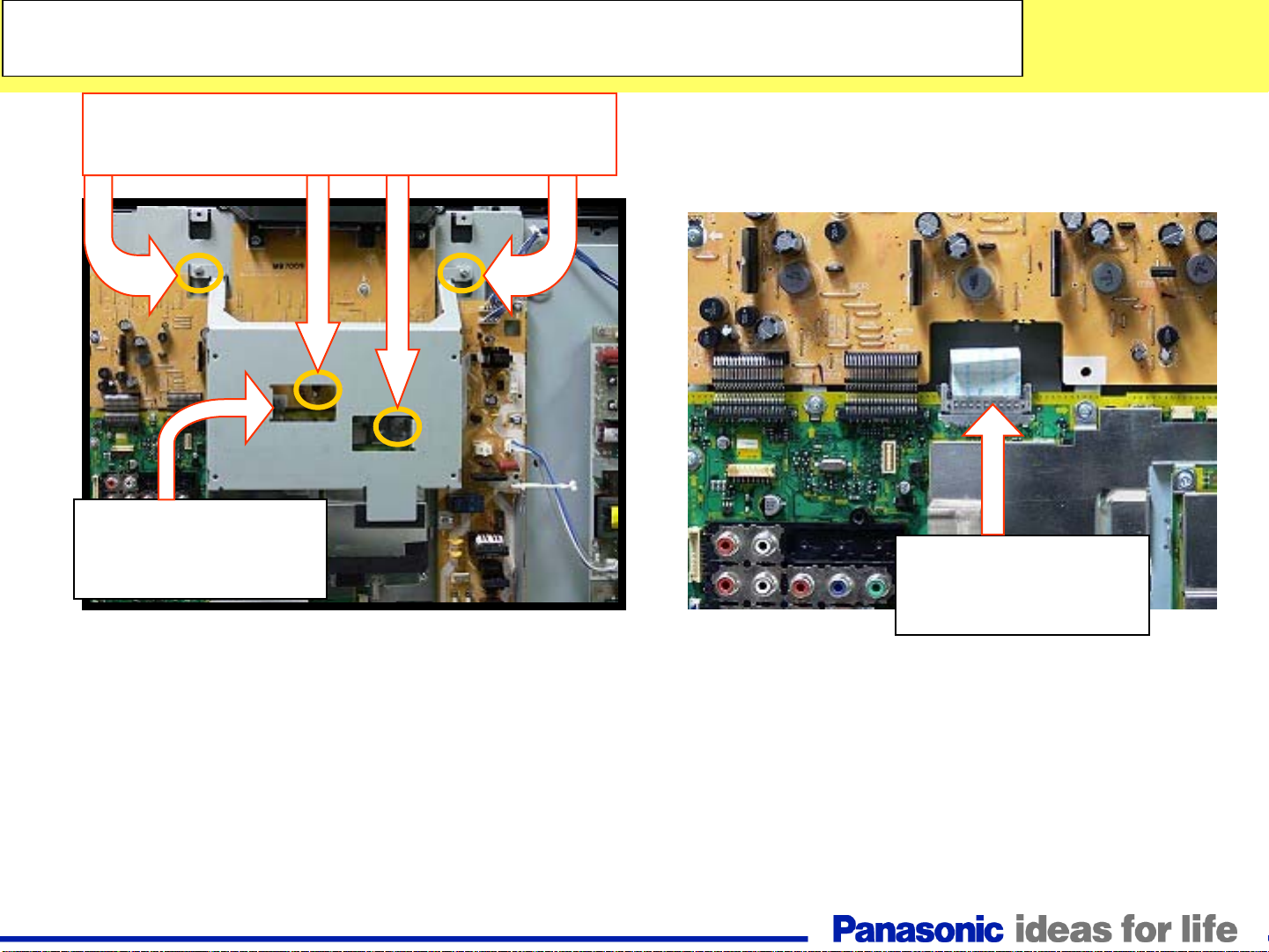
P.C.B Layout (LX700 LVDS Connector)
P.C.B Layout (LX700 LVDS Connector)
Remove the 4 Screws and the metal
plate to expose the LVDS Connector.
A2
LVDS Connector
A2
LVDS Connector
12
Page 13
TC-32LX700 Board Description
Board Description Part Number
A-Board
AP-Board DC-DC, Power Switch
DT-Board Digital Tuner (Exchange Only)
G-Board Video 3, Headphone Jack
GS-Board SD Card Slot
V-Board Remote Receiver, LED
P-Board Power (AC/DC) (Exchange Only)
Control Panel
ASSY
Main (Rear Terminal, AV Switch, MCU, Audio &
Video Processor, LVDS) (Exchange Only)
Control Button (Non-Serviceable, Control Panel
Assembly should be exchanged for service.)
TNPH0683S
TNPA4155ABS
TNAG172S
TNPA4266S
TNPA4206S
TNPA4152ADS
TZRXN010MRR
K0RB00600004
13
Page 14
Differences from Current models
Differences from Current models
LX600
LX60
A
VCTP
AUDIO
SWITCH
HDMI
(CEC)
Differences from LX600/60:
FPGA
DT
ATSC
Peaks Lite
A
AUDIO
SWITCH
VIDEO
SWITCH
LX700
LX70
Peaks Lite2
HDMI
(CEC)
HQ1L(*)
DT
* 32LX700 only
LVDS TX(*)
ATSC
1. Peaks Lite2 and VIDEO SW are introduced instead of VCTP, FPGA and Peaks Lite .
2. For LX700, HQ1L and LVDS TX are introduced for Motion Picture Pro.
3. HQ1L and LVDS TX are used to convert the picture frames from 60 to 120.
This process helps to reduce after-images.
4. The DT board of the 32LX700 provides Channel Data output only. The
MPEG2 and AC3 (Peaks Lite2) decoders are now part of the A board.
14
Page 15
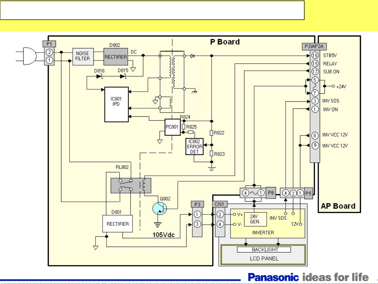
P Board ––
P Board
Main Power Board
Main Power Board
T801
D821
15
Page 16

P Board ––
P Board
When AC is applied to the TV, the Standby circuit of the P board outputs 5Vdc to the AP board. The STB5V
passes through the AP board and enters the A board. On the A board The STB5V is converted to 3.3V to power the system
control circuit for standby operation. The STB3.3V is also applied to the Remote Control receiver and the power LED on the
V board. The MPU (IC1100) of the A board outputs the SUB_ON command to provide a ground connection to relay RL802
of the power supply board. On the AP board, the SUB_ON command is used to turn on a circuit (not shown in the diagram)
that provides STB5V to relay RL802 via pin 15 of connector AP2/P2. When the relay is closed, DC voltage from the rectifier,
approximately 105Vdc, is supplied to the LCD panel for conversion into 24Vdc. The output of the 24V generator passes
through the P board and enters the AP board for conversion into SUB_5V, DTV9V (SUB_9V), and HQ3.3V.
If the power button (main unit or remote control) is not pressed within 25 seconds after applying AC to the unit,
the SUB_ON command goes low to disengage the power relay. When the power button is pressed, the SUB_ON command
goes high to repeat the same operation. The voltages remain present until the unit is turned off.
When the unit is turned on, the LCD panel’s inverter circuit uses the 24Vdc source to generate the 120Vac to
illuminate the CCFLTs. The INV_ON command and the 12Vdc source enter the panel’s drive circuit via the connector
AP2/P2 and P5 of the P board. The inverter circuit is monitored for abnormality. When a defect is detected, a SOS (High)
output is provided to the A board MPU (IC1100) via Connectors P5 and P2/AP2.
Main Power Board
Main Power Board
Caution: The P board is not to be repaired by you. It is to be exchanged only.
16
Page 17
Main MPU (Power On Commands)
Main MPU (Power On Commands)
17
Page 18

Main MPU (Power On Commands)
Main MPU (Power On Commands)
The STB 5V output of the P board passes through the AP board and enters the A board when the unit is
plugged into the AC outlet. IC5702 of the A board converts the STB 5V to 3.3V to power the system control circuit.
Activation of the power switch causes transistor Q5712 to turn off and output STB 3.3V to pin 18 of the MPU. Upon
receiving the STB 3.3V, the MPU (IC1100) outputs the TV-SUB-ON command via pin 8 of connector A4/AP4. The TVSUB_ON command is routed to the P board to provide a ground connection for relay RL802 of the power supply board.
On the AP board, The TV_SUB_ON command is used to turn on a circuit (not shown in the diagram) on the A board
that provides STB_5V to relay RL802. As a result , the switch of relay RL802 on the P board closes to allow the output
of 105Vdc to the LCD panel. The TV_Main_ON signal issued by IC1100 appears on pin 6 of connector AP4/A4 to
enable the output of the sound+12V DC/DC converter. Pin 105 of IC1100 outputs the PANEL VCC command to the AP
board to turn on the 12V DC/DC converter. The 12V output is provided to the panel via the P board.
Caution: Measure the 105Vdc source between pin 1 and 3 of connector P3. Hot ground must be used.
18
Page 19
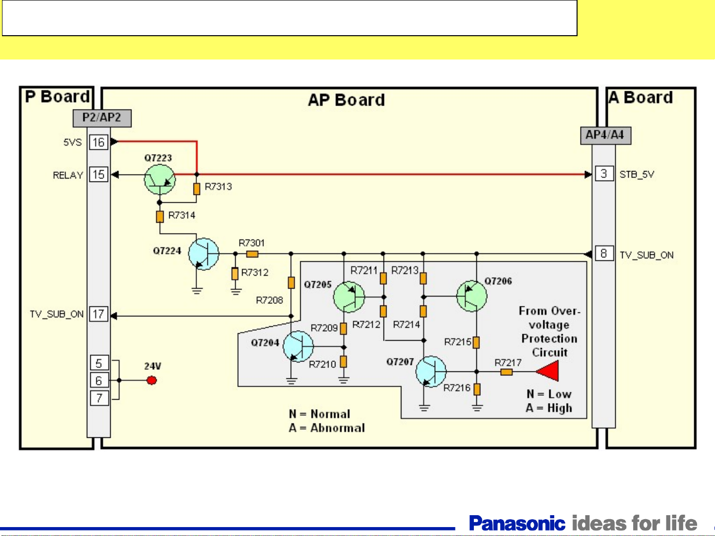
Standby Operation
Standby Operation
19
Page 20

Standby Operation
Standby Operation
When the main power switch is activated, it is sensed on the A board by the MPU IC1100. The TV_SUB_ON
signal is subsequently issued in response on pin 8 of connector A4/AP4. It turns on the transistors Q7224 and Q7223 to
output the “Relay voltage on pin 15 of connector AP2/P2. The TV Sub_On signal is also provided to the relay via the
resistor R7208 and pin 17 of connector AP2/P2. This pulls the contacts of the AC relay on the P board. The AC input is
rectified and provided to the LCD panel for conversion into 24Vdc. The 24V is then provided to the inverter circuit of the
LCD panel to produce the 120Vac that powers the backlight CCFLTs. The same 24V passes through the P board and
enters the AP board for conversion into other voltages.
The over-voltage protection circuitry affiliated with each of the regulators located on the AP board monitors
for over-voltage conditions. It is designed to turn off the AC power by disabling the SUB_ON command that turns on the
AC relay.
When an over-voltage condition is detected on the AP board, the voltage at the base of transistor Q 7207
goes “high” to turn on Q7207, Q7206, Q7205, and Q7204. The TV_SUB_ON voltage at pin 17 of connector A2/AP2 is now
grounded through Q7204 and the unit shuts down. To turn the unit back on, disconnect and reconnect the AC cord before
pressing the power button.
20
Page 21
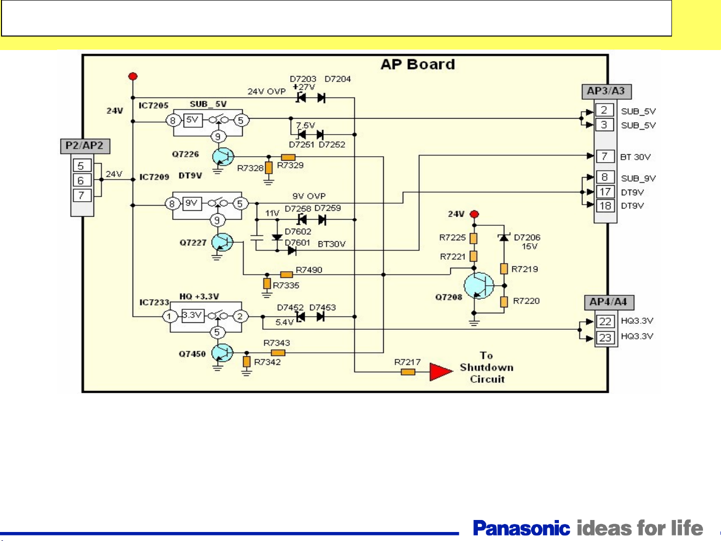
SUB Voltages and Over--
SUB Voltages and Over
voltage Protection
voltage Protection
The AP Board is responsible for the regulation, distribution and dissemination of all secondary
voltages derived from the 24V output of the P Board. During standby operation, the 24V output of the P board
biases the transistor Q7208 into operation, causing its collector to become “low”. The low at the collector of Q7208
causes the transistors Q7226, Q7227, and Q7450 to turn off. As a result, IC7205, IC7209, and IC7233 go into
operation to immediately provide the Sub_5V, DT9V, BT30V, and HQ 3.3V output.
The over-voltage protection circuitry affiliated with each of the regulators monitors for excessive current and overvoltage conditions. It is designed to turn off the AC power by disabling the SUB_ON signal needed to turn on the AC
relay.
21
Page 22
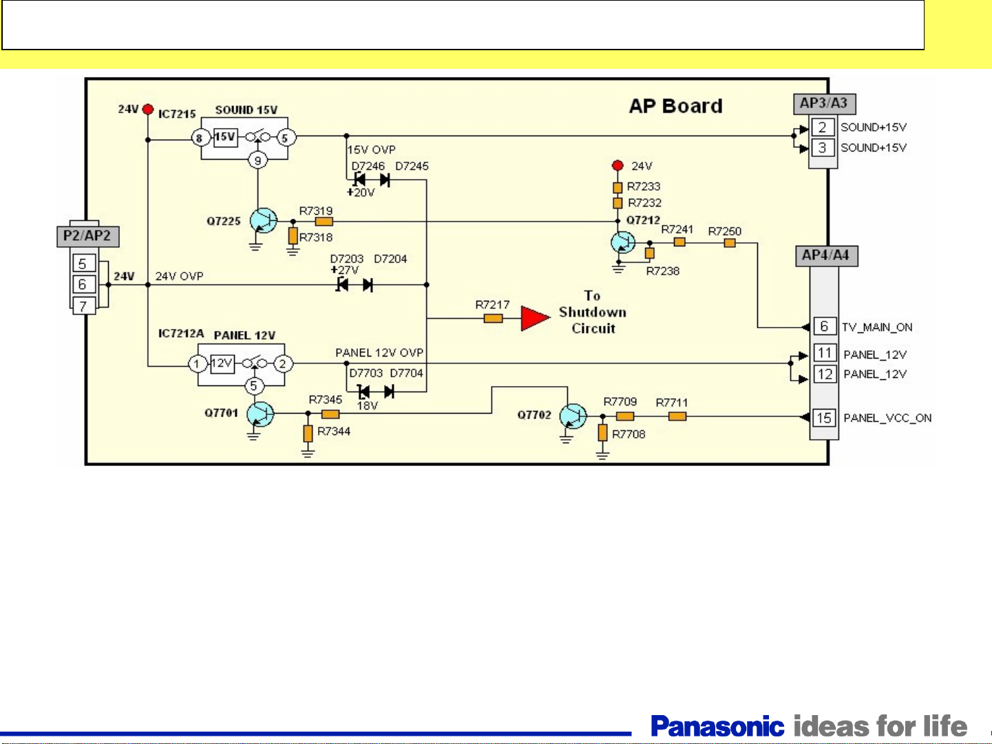
Main Voltages and Over--
Main Voltages and Over
voltage Protection
voltage Protection
When the unit is turned on, the TV_Main_On command (high) of IC1100 biases the transistor Q7212
into operation, causing its collector to go “low”. The low at the collector of Q7212 causes the transistor Q7225 to turn
off. As a result, IC7215 goes into operation to provide the Sound_15V output.
When the Panel_VCC_On command is issued, transistor Q7702 turns on causing Q7701 to turn off.
Consequently, IC7212 turns on and outputs 12V. This voltage enters the A board via the connector AP4/A4. It is also
provided to the LCD panel via the connector AP2/A2, the P board, and the connector P5 (not shown in the diagram).
The over-voltage protection circuitry affiliated with each of the regulators monitors for excessive current
and over-voltage conditions. It is designed to turn off the AC power by disabling the SUB_ON signal needed to turn
on the AC relay.
22
Page 23
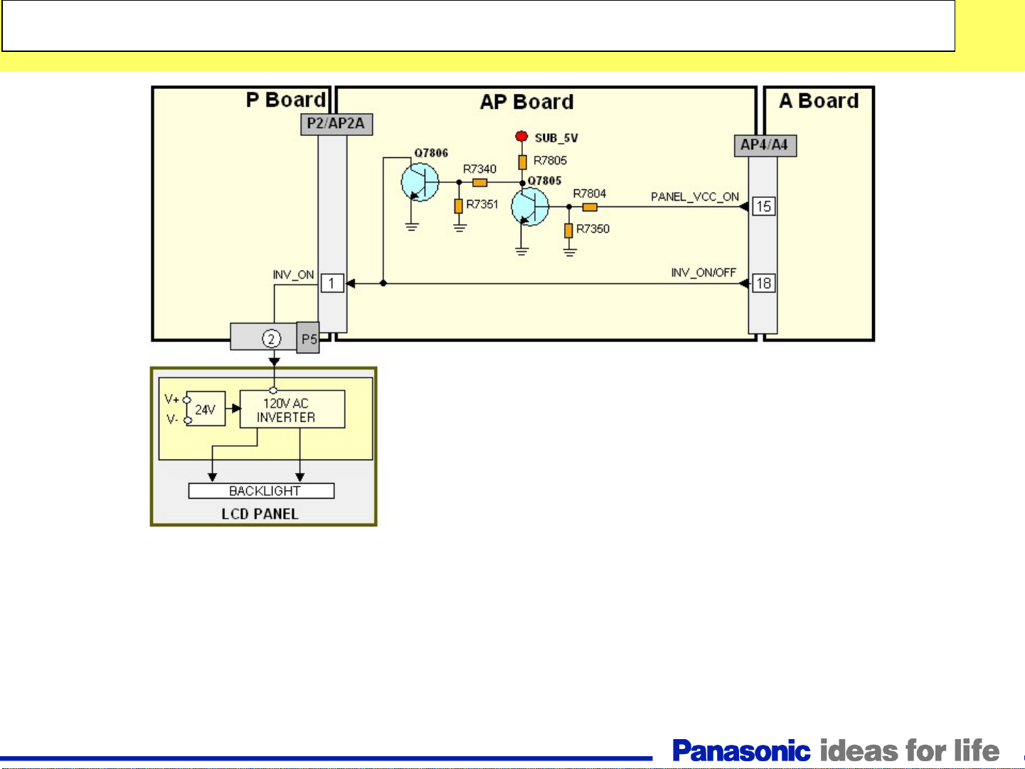
Inverter_On Command and Protection
Inverter_On Command and Protection
The INV_ON/OFF command (high) of the MPU, IC1100 of the A board, passes through the AP
and P boards before entering the LCD panel. On the LCD panel, it triggers the operation of the inverter to
produce the 120V AC that powers the backlight CCFLTs.
To avoid catastrophic failures, when the Panel_VCC_ON pin of the MPU goes “low”, Q7805 turns off.
Consequently, Q7806 turns on to disable the operation of the inverter.
23
Page 24

Purposely Left Blank
Purposely left blank
Page 25
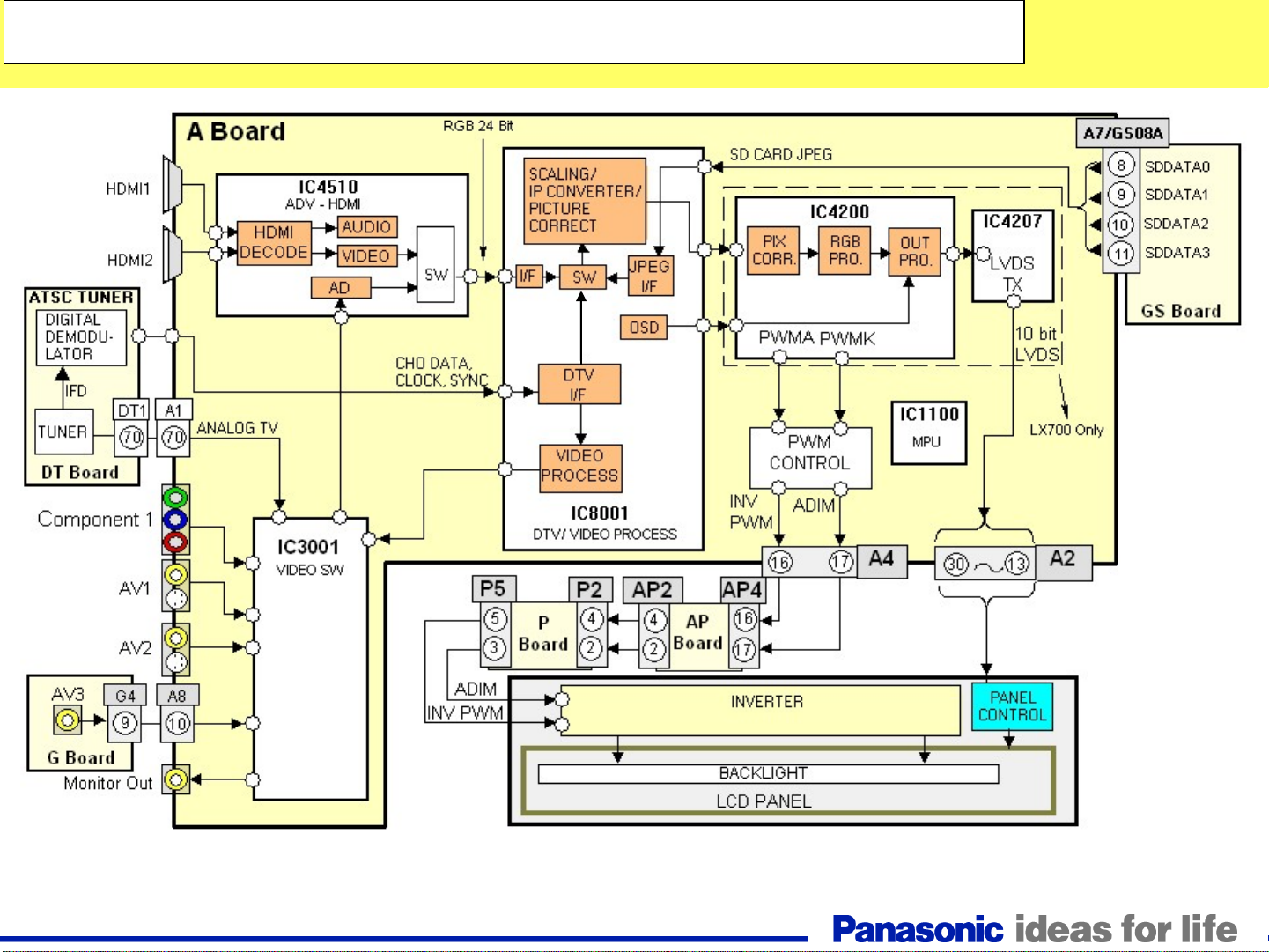
Video Process Block Diagram
Video Process Block Diagram
25
Page 26
Video Process Block Diagram
Video Process Block Diagram
The main function of the A board is to select and process one of the incoming video signals. Video inputs,
component video Input, and the composite video output of the tuner are all connected to IC3001 for selection. The video
output signal of the switch can be in any of the three formats: Video, Y/C, or Y, Pb, Pr. The selected output enters IC4510,
the HDMI IF Receiver/Decoder IC, for A/D conversion. The comb filter inside IC4510 converts the composite video signal of
the main picture to Y and C (luminance and chrominance) signals. S-Video, which is already Y/C separated, simply passes
through the comb filter. The chrominance data is then applied to the Chroma Demodulator circuit to separate the color signal
into Pb and Pr data. At the completion of this process , the format of the composite or S-Video signal is now the same as a
digital 480i component signal. If the incoming video is in the 480p, 720P, or 1080i format, the Y, Pb, and Pr signals undergo
A/D (analog to digital) conversion only. The 10 bit YUV data is provided to a video switch. The HDMI receiver section of
IC4510 converts the incoming HDMI signals to a YUV video signal. The Video interface circuit selects between the two HDMI
sources and outputs the YUV signal to the switch. The output of the switch is provided to the PEAKS LITE IC, IC8001.
Digital television reception of the tuner is output in the form of a transport stream (CHODATA). The transport
stream enters the DTV I/F (Interface) section of IC8001 where the video signal is extracted and converted to YUV data. The
output is provided to the Video Input switch for selection. The JPEG data of the GS board enters the JPEG I/F section of
IC8001 for conversion into YUV data and output to the video switch. The video switch outputs the selected picture data to the
Video Process circuit.
The Video Process section of the IC performs all picture control operations such as brightness, contrast, color,
tint, etc. The output signal is then applied to the HQ1L circuit (IC4200) for frame doubling operation. IC4200 is the circuit
responsible for the Motion Picture Pro operation that reduces afterimage by 50%. On Screen Display data such as channel
numbers, Digital TV closed caption, and picture adjustments are mixed with the video data. The output of IC4200 is provided
to the LVDS transmitter (IC4207). The transmitter distributes signals with low-jitter, while creating little noise. It reduces
power consumption and the generated noise from data transmission. Another benefit of the LVDS standard is minimal
concern for cable length.
The main MCU (IC1100) controls the entire operation of the A board. It serves as the controller that monitors all
operations of the TV section (not display) of the unit. When watching digital television or viewing pictures from an SD card,
the video process section of IC8001 converts the digital video into analog composite video signal for output at the monitor out
jack.
26
Page 27
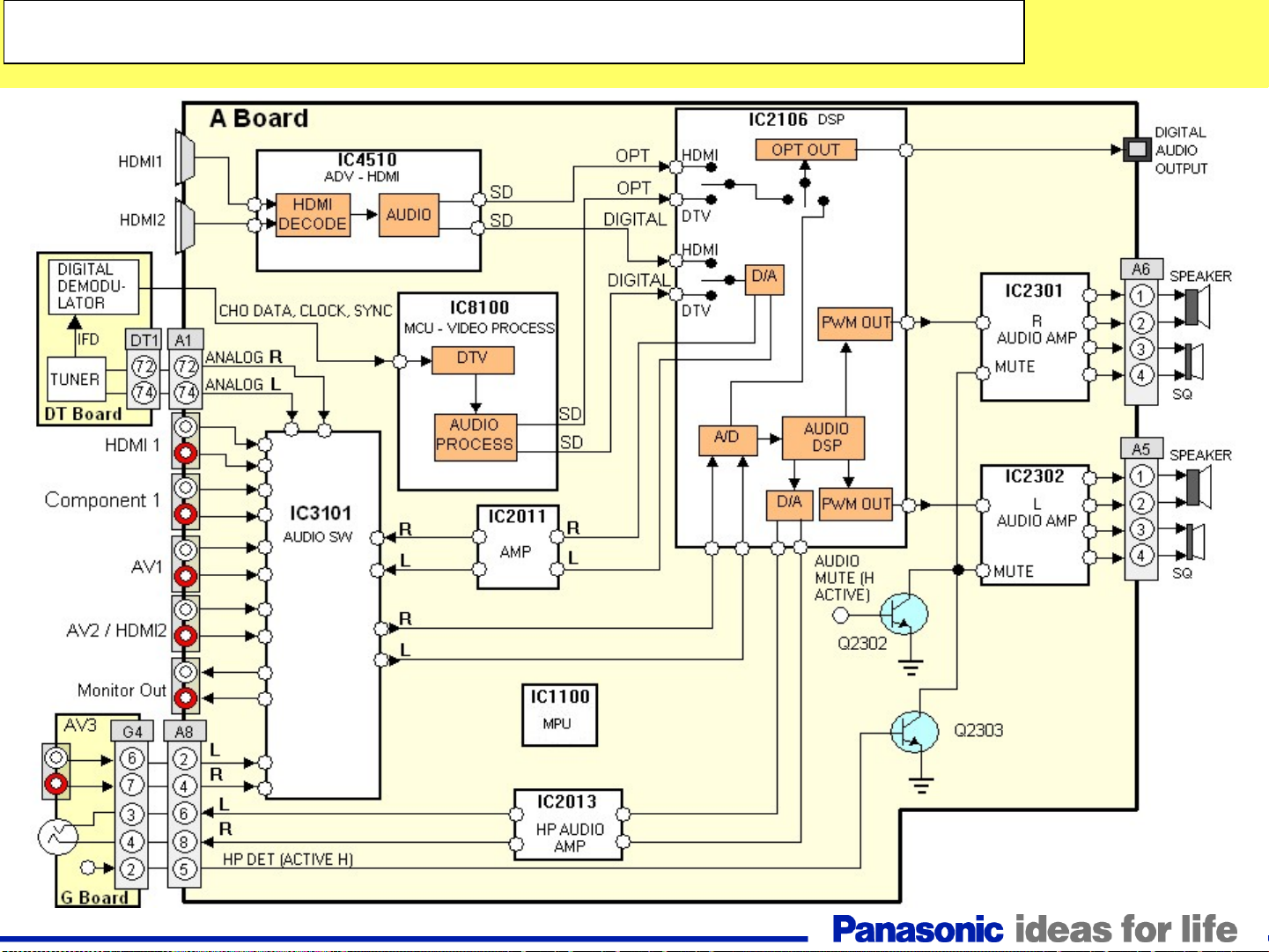
Audio Process Block Diagram
Audio Process Block Diagram
27
Page 28

Audio Process Block Diagram
Audio Process Block Diagram
IC3101 of the A board handles the audio selection of most inputs. Analog audio of the tuner and audio signals
from composite, component, and DVI inputs are connected to IC3101 for selection. The output of IC3101 enters IC2106 and
undergoes analog to digital conversion. The serial data output is provided to the audio DSP (Digital Signal Processor).
Volume, bass, treble, and balance adjustments of the audio signal are performed by this circuit. The output is two channel
PWM data that are applied to IC2301 and IC2302 for amplification. The PWM output signals of the power amplifiers are
output to the right and left channel speakers for sound reproduction. The HDMI receiver section of IC4510 converts the
incoming HDMI audio into serial data. The Audio interface circuit selects between the two HDMI audio and outputs the SD
(serial Data) to the switch located inside IC2106. Two outputs are provided, one for the digital audio output jack, the other for
the speakers. Digital television reception of the tuner is output in the form of a transport stream that contains MPEG2 video
and AC3 audio. The transport stream enters the DTV I/F section of IC8001 where the audio signal is extracted and converted
to serial data. Two outputs are provided to IC2106. One output consists of the AC3 audio that will be provided to the digital
audio output jack. The other output consists of left and right audio that will be used to drive the speakers. Speaker output of
the DTV and HDMI audio is selected and converted to analog. The analog audio is then output to an audio amplifier (IC2011)
and then applied to the audio selector (IC3101). The optical jack audio signal is also selected and processed inside IC2106.
Q2303 is a muting transistor that applies a low to IC2106 when a headphone jack is connected to the unit. Q2302 applies a
low to IC2106 when the mute function of the unit is active.
28
Page 29
MPU SOS Inputs and Blink Codes
MPU SOS Inputs and Blink Codes
29
Page 30

MPU SOS Inputs and Blink Codes
MPU SOS Inputs and Blink Codes
One Blink: One blink of the power LED indicates a problem in the inverter circuit located on the LCD panel. The inverter
board is not to be repaired in the field. Therefore a replacement is required.
Three Blinks: Three blinks of the power LED indicates an over-current or over-voltage condition in one of the DC supplies
of the AP board. The AP board is repairable. Therefore the use of an ohmmeter and peak-hold-voltmeter is required to
determine the cause of the shutdown. An over-voltage condition is definitely a defect of the AP board. An over-current
condition may be due to a short circuit located in the AP board, A board, or the LCD panel.
Five, Seven, or Eight Blinks: The A board is responsible for five, seven or eight blinks of the power LED. The MAIN +3.3V,
MAIN +5V, and MAIN +9V sources are all produced on the A board. The detection input pins of the MPU, IC1100, monitor
for their presence.
Four or Six Blinks: The AP board is responsible for four or six blinks of the power LED. The DTV9V, and SUB_5V
sources are produced on the AP board. The MPU IC1100 monitors for their presence when the unit is connected to AC
Power. A short or open circuit on the A board may also be responsible for their absence.
Nine Blinks: Nine blinks of the power LED is due a short circuit in the audio output circuit (s) of the unit. The audio output
circuit is located on the A board. Confirm the status of the speakers. If defective, perform a replacement. If ok, replace the A
board.
Ten Blinks: Ten blinks of the power LED indicates a malfunction of IC4200, the frame converter. This IC resides on the A
board. Therefore ten blinks of the power LED requires the replacement of the A board.
30
Page 31

Over--
Over
Current Protection Circuit
Current Protection Circuit
31
Page 32

Over--
Over
BT30V, and the Panel VCC sources. If any of these voltage sources goes low, Q7210 turns on. As a result, the collector of
Q7210 goes high to signal a shutdown condition to IC1100 on the A board. The T V_SUB_ ON pin of IC4002 goes low to deactivate the AC relay on the P board.
causing its collector to become “low”. The low at the collector of Q7208 causes the transistors Q7450 to turn off. As a result,
IC7233 goes into conduction to immediately provide the HQ 3.3V output. When the 24 drops below the reverse breakdown
voltage of D7206, transistor Q7208 turns off and transistor Q7450 turns on. IC7233 ceases to operate causing Q7451 to turn
off and Q7452 to turn on. Consequently, the SUV_9V line is now grounded. Diode D7220 becomes forward biased and
Q7210 outputs a high to trigger the shutdown of the unit.
Current Protection Circuit
Current Protection Circuit
The protection shutdown circuit is designed to monitor for a short or loss of the SUB_9V, SOUND_VCC,
During standby operation, the 24 volt output of the P board biases the transistor Q7208 into conduction,
32
Page 33

Over--
Over
Current Protection Circuit 2
Current Protection Circuit 2
33
Page 34

Over--
Over
Sound_VCC Protection
causing its collector to become low. The low at the collector of Q7208 causes the transistor Q7214 to turn off. When
the PANEL_MAIN_ON command (high) is issued Q7212 turns on. Consequently Q7225 turns off, and IC7215 goes
into conduction to provide the SOUND_15V output.
ground the PANEL_MAIN_ON voltage. Q7212 turns off and Q7225 turns on. IC7215 ceases to operate and the
Sound_VCC is no longer output.
and R7492 receives 12V. Due to this condition, the transistor Q7210 remains off. If the SOUND_15V line becomes
shorted, diode D7469 goes into conduction to turn Q7210 on. Consequently Q7210 outputs a high to shut down the
unit.
Panel_VCC Protection
causing its collector to become low. The low at the collector of Q7208 causes the transistor Q7508 to turn off. When
the PANEL_VCC_ON command (high) is issued, Q7702 turns on. Consequently Q7701 turns off, and IC7212 goes
into conduction to provide the PANEL_12V output.
ground the PANEL_VCC_ON voltage. Q7702 turns off, and Q7701 turns on. IC7212 ceases to operate and the
Panel_VCC is no longer output.
and R7488 receives 12V. Due to this condition, the transistor Q7210 remains off. If the Panel_12V line becomes
shorted, diode D7472 goes into conduction to turn Q7210 on. Consequently Q7210 outputs a high to shut down the
unit.
operation, causing its collector to become “low”. The low at the collector of Q7212 causes the transistors Q7225 to
turn off. As a result, IC7215 goes into operation to provide the Sound_15V output.
Current Protection Circuit 2
Current Protection Circuit 2
During normal operation, the 24 volt output of the P board biases the transistor Q7208 into conduction,
When the 24 drops below the reverse breakdown voltage of D7206, Q7208 turns off, Q7214 turns on to
During normal operation, the anode of D7469 receives 5V and the junction of D7469, D7470, R7486,
During normal operation, the 24 volt output of the P board biases the transistor Q7208 into conduction,
When the 24 drops below the reverse breakdown voltage of D7206, Q7208 turns off, Q7508 turns on to
During normal operation, the anode of D7472 receives 5V and the junction of D7472, D7473, R7493,
When the unit is turned on, the TV_Main_On command (high) of IC1100 biases the transistor Q7212 into
34
Page 35

Power LED Timing Table
35
Page 36

Power LED Timing Table
36
Page 37

Self-Check and Reset Function
Self-Check Function:
1. Checks the communication IIC bus lines
2. Provides a SOS History
To Access the Self-Check Mode: Turn the TV on and select an
To Access the Self-Check Mode
active channel. While pressing the “VOLUME ( - )” button on the main
active channel. While pressing the “VOLUME ( - )” button on the main
unit, press the “OK” button on the remote control for more than 3
unit, press the “OK” button on the remote control for more than 3
seconds.
seconds.
This procedure is useful to display the unit’s firmware version and check IC data
communications.
To Reset the unit: Turn the TV on and select an active channel.
To Reset the unit: Turn the TV on and select an active channel.
: Turn the TV on and select an
While pressing the “VOLUME ( - )” button on the main unit, press the
While pressing the “VOLUME ( - )” button on the main unit, press the
“Menu” button on the remote control for more than 3 seconds.
“Menu” button on the remote control for more than 3 seconds.
The Reset function clears channel programmed settings, picture settings, channel
labels, LOCK mode settings, and password.
It restores the unit to factory shipping settings.
To Exit the Self-Check Mode, Disconnect the AC cord from the wall outlet.
To Exit the Self-Check Mode, Disconnect the AC cord from the wall outlet.
37
Page 38

Self-Check Menu
SELF CHECK ----.XXXXXX-XXXXXX
DT OK
HQ1L OK
ADV OK
VSW OK
ADAV OK
ASW OK
TUN1 OK
TUN2 OK
FE OK
GenX4 OK
MEM1 OK
MEM2 OK
Copyright 2007 Matsushita Electric Industrial Co., LTD
38
Page 39

Check Point
A-Board
39
Page 40

Serviceman Mode
To enter the Serviceman Mode, turn the TV on and while
To enter the Serviceman Mode, turn the TV on and while
pressing the “VOLUME ( - )” button on the main unit, press the
pressing the “VOLUME ( - )” button on the main unit, press the
“RECALL” button of the remote control three times within 3 seconds.
“RECALL” button of the remote control three times within 3 seconds.
To exit the Serviceman Mode, Press the Power button on the
To exit the Serviceman Mode, Press the Power button on the
TV or the Remote Control.
TV or the Remote Control.
40
Page 41

Serviceman Mode Menu and Navigation
SERVICE
ADJUST
WB-ADJ
0PTION
RM-SET
SRV-TOOL
Peaks Soft 0.270
Peaks EEP 1.00
LSI DATA 0.00.36
GenX SOFT 0.23.00
GenX EEP 0.40.00
GenX COR 0.00.00
HQ1L EEP 15
Key command
“1” button...Main items Selection in forward direction
“2” button...Main items Selection in reverse direction
“3” button...Sub items Selection in forward direction
NOTE: This is
not part of the
Menu.
“4” button...Sub items Selection in reverse direction
“VOL” button...Value of sub items change in forward direction ( + ), in
reverse direction ( - )
41
Page 42

Adjustment Data
MAIN ITEM
SUB ITEM
ADJUST
CONTRAST
0000
DATA
YMAX
“1” or “2” button of the remote control to select the main Adj. item
“3” or “4” button of the remote control to select the sub Adj. Item
“Vol. (-)” or” Vol. (+)” to change the data
Note: Record the original data on a sheet of paper prior to making any adjustment.
42
Page 43

SRV-TOOL
SRV-TOOL
TD2Microcode: 81c0000e
Flash ROM: 1- 227E
PCTC: 00 . 00 . 00 . 00 . 00 Time 000040:40 Count 0000049
To access:
1. Select “SRV-TOOL” in the Serviceman Mode menu.
2. Press the [OK] button on the remote control.
43
Page 44

SRV-TOOL
Display of SOS History
SOS History
(Number of LED blinking) indication. From the left side; Last SOS, before Last, third
occurrence before last, 2
indication will be cleared by entering the “Self-check mode. The unit will be forced to
factory shipment setting”.
POWER ON TIME/COUNT
Time: Cumulative power on time, indicated in decimal numbers__ hour: minute
nd
occurrence after shipment, 1
st
occurrence after shipment. This
Count: Number of power on/off times in decimal numbers
This indication will not be cleared by self-check or any command.
Exit:
Disconnect the AC cord from wall outlet.
44
Page 45

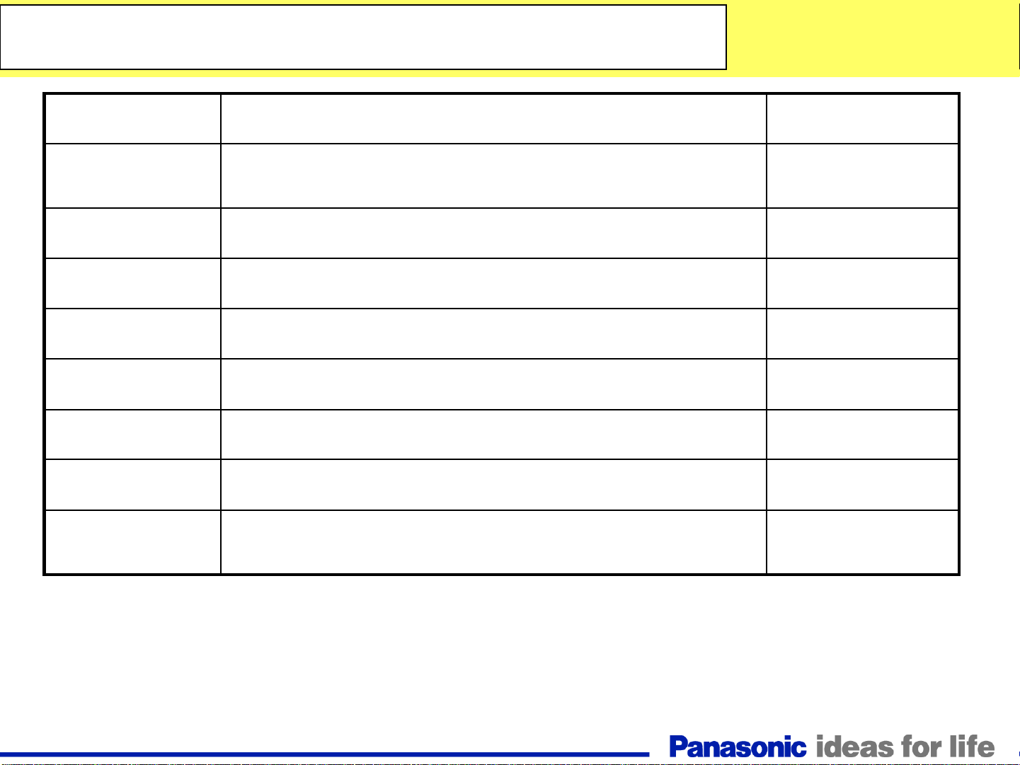
Voltage Chart of AP-board
AP-board
VOLTAGE TEST POINT SPECIFICATION CONNECTOR
24V TP7904 24.0 ± 1.2V AP2 _PIN 1, 2, 3
SUB_5V TP7211 5.12 ± 0.25V AP3_PIN 21, 22
SUB_9V TP7213 9.27 ± 0.45V AP3_PIN 8, 17, 18
BT_30V TP7601 31.5 ± 2.5V AP3_PIN 7
HQ_3.3V TP745 3.38 ± 0.17 A-Board
SOUND_15V TP7209 15.2V ± 0.75V AP3_PIN 2, 3
PANEL_12V TP7702 12.14 ± 0.6V AP4_PIN 11, 12
STB_5V TP7151 5.0 ± 0.5V AP4_PIN 3
45
Page 46

Voltage Chart of P and A boards
P-board
VOLTAGE TEST POINT SPECIFICATION
STB_5V TP823 5.0 ± 0.5V
A-board
VOLTAGE TEST POINT SPECIFICATION
STB3.3V TP7006 3.3 ± 0.16V
SUB1.2V TP5601 1.26 ± 0.06V
SUB1.8V TP5602 1.83 ± 0.09V
SUB3.3V TP5600 3.3 ± 0.16V
MHQ1.2V TP4209 1.22 ± 0.06V
MHQDDR2.5V TP4210 2.5 ± 0.12V
46
Page 47

Voltage Chart of DT board
A-board
VOLTAGE TEST POINT
A- BOARD
SUB_3.3V TP8332 3.3 ± 0.16V
SUB_1.2V TP8328 1.26 ± 0.06V
SUB_5V TP8326 5.12 ± 0.25V
30V_A TP8331 31.5 ± 2.5V
DT-board
SPECIFICATION
47
Page 48

Purposely Left Blank
Purposely left blank
Page 49

Troubleshooting Signal Problems
Troubleshooting Signal Problems
We can classify the signal problem into three categories. It is important to check all
functions to determine whether both picture and sound problem exist. Checking all
functions helps us determine whether the cause of the problem is the panel, the video
processor or sound processor.
Picture NG and Sound OK
1)
Picture OK and Sound NG
2)
Picture NG and Sound NG
3)
49
Page 50

Picture
Picture
NG
NG
and Sound
and Sound
OK (LX700/LX70 )
OK (LX700/LX70 )
Is there a
picture from any
of the inputs?
No
No picture but
is there OSD?
Yes
A Board
Yes
No
No picture from
the AV Terminal
No Picture
from Analog TV
No Picture from
Digital TV
No Picture from
HDMI Input
LCD Panel or A board
A Board
a picture from the
A Board
Is there
No
A Board
AV Terminals?
Yes
See slide “No Picture from TV Reception”
HDMI I/F
A
HDMI
HDMI
DT
TU8300
TUNE
R
AV1
AV2
COMPONENT
Monitor Out
G
AV3
1
2
IC8302
FRON
END
PROCES
S
A/D
IC3001
T
VIDEO
SWITCH
IC4510
SW
50
IC4200
HQ1L
IC8001
Peaks Lite2
SCALING/
IP CONVER
TER/
PICTURE CORRECT/
OSD
VIDEO PROCESS
DTV
IC4207
LVDS TX
LVDS
IC1100
STB
MCU
Analog
Digital
LCD
Panel
GS
LX700
Only
Page 51

Picture OK and
Picture OK and
Sound NG
Sound NG
(LX700/LX70)
(LX700/LX70)
Is there
sound from any of the
input sources?
No
Is there sound
from the
headphone?
Yes
A Board
No
Yes
from any of the AV
from analog TV
No sound
from Digital TV?
No Sound
from HDMI Input
of the AP board. Refer to
Slide 43 for test point
No sound
terminals.
No sound
Is there 15V
on connector AP3
locations
Yes
A Board or Speaker
A Board
Is sound
from any of the AV Terminals
OK?
Yes
DT Board
Is sound
from any of the AV Terminals
OK?
Yes
A
DT Board
HDMI1
HDMI2
A Board
DT
TU8300
TUNER
IC830
2
No
AV1
AP Board
AV2
COMPONEN
T
MONITOR OUT
AV3
G
G
HEADPHONE
FRON
T
END
No
L/R
L/R
L/R
L/R
L/R
L/R
IC451
0
HDMI I/F
IC3101
AUDIO
SWITCH
HP AMP
A Board
No
A Board
IC2106
Audio DSP
IC8001
Peaks Lite2
AUDIO
PROCESS
DTV
IC2301
AUDIO
AMP
IC2302
AUDIO
AMP
IC1100
STB
MCU
Analog
Digital
LX700 Only
51
Page 52

Picture NG
Picture NG
and
and
Sound NG
Sound NG
(LX700/LX70 )
(LX700/LX70 )
Input Source
check
Analog TV
Picture NG
Sound NG
AV Terminal
Picture NG
Sound NG
HDMI Input
Picture NG
Sound NG
Digital TV
Picture NG
Sound NG
AV Terminal
Picture &
Sound OK?
Yes
DT Board
A Board
A Board
AV Terminal
Picture &
Sound OK?
Yes
No
No
A Board
A Board
: Line where problem might occur
IC4510
IC451
0
HDMI I/F
L/R
A/D
IC3001
VIDEO
SWITCH
IC3101
HDMI I/F
SW
IC4200
HQ1L
IP CONVER
TER/
PICTURE CORRECT/
OSD
VIDEO PROCESS
DTV
IC2106
Audio DSP
IC4207
LVDS TX
IC8001
SCALING/
IC2301
AUDIO
AMP
IC2302
AUDIO
AMP
LVDS
IC1100
STB
MCU
A
HDMI1
HDMI
2
DT
TU8300
TUNE
R
AV1 GS
AV2
COMPONENT
Monitor Out
G
A
DT
TU8300
TUNER
AV3
HDMI1
HDMI2
IC830
2
TU8302
FRON
T
END
FRON
T
END
PROCES
S
Analog
Digital
LCD
Panel
LX700 Only
Analog
Digital
DT Board
52
AV1
AV2
COMPONEN
T
MONITOR OUT
AV3
G
G
HEADPHONE
L/R
L/R
L/R
L/R
L/R
AUDIO
SWITCH
HP AMP
IC8001
Peaks Lite2
DTV
AUDIO
PROCESS
IC1100
STB
MCU
LX700 Only
Page 53

No Picture from TV Reception
Is there video from
any of the inputs?
Yes
Check for the BT30V, DTV_9V, and
SUB_5V on connector AP3
of the AP board. Refer to Slide 45 for test
point locations.
No
See the
troubleshooting
flowchart for No
picture.
Yes
Are SUB_3.3V
and SUB_1.2V present
on the A board? Refer to
Slide 46 for test
point locations.
Yes
Replace the DT board
Are DTV 9V
And SUB
5V OK?
Yes
No
No
Replace the A board
Replace defective Regulator and
biasing components. Reference
the power distribution diagram on
Slide 21.
Is the
BT30V
source
OK?
53
No
Check the cathode of D7601
on the AP Board. Cathode of D7601
should measure 30V. If not, repair the DTV9V
DC/DC converter.
Page 54

No Picture
Is there picture from
any of the inputs?
Yes
Check for the BT30V, DTV_9V, and
SUB_5V on connector AP3
of the AP board. Refer to Slide 45 for test
point locations.
No
See the
troubleshooting
flowchart for No
picture.
Yes
Are
SUB_3.3V
SUB_1.2V
OK?
Yes
Replace the DT board
Are DTV 9V
And SUB
5V OK?
No
No
Replace the A board
Yes
No
Is the
BT30V
source
OK?
Replace defective Regulator and
biasing components. Reference
the power distribution diagram on
Slide 21.
54
Check the cathode of D7601
on the AP Board. Cathode of D7601
should measure 30V. If not, repair the DTV9V
DC/DC converter.
Page 55

No Video, Dark Blue Screen
Try using a different video input source.
Try the Tuner, Component, S-Video or
HDMI input.
Does any
input
work?
No
Yes
Check the video input connections and
termination points for a possible cold
solder joint or connection problem.
Replace defective Regulator and
biasing components. Refer the
power distribution diagram on Slide
21.
Check for the BT 30V, SUB 9V, &,
SUB5V sources on connector AP3
of the AP board. Refer to Slide 45 for test
point locations.
No
BT30V,
SUB9V
SUB5V
OK?
Yes
Continued on next
page
Did this
fix the
problem?
No
Replace the A
Board.
Yes
Problem Solved
55
Page 56

No Video, Dark Blue Screen (Continued)
From the last page
Remove the metal plate
From where it sits on the A board in order to
access the LVDS connector. There are four
screws that need to be removed. See slide 12.
Confirm the connection of the
LVDS Connector (CN A2).
Is the picture
restored?
No
Replace the A board.
56
Yes
Problem Solved
Page 57

No Audio
Problem
Solved
A Board
Determine which audio input is
defective. Check for poor solder
connections in the vicinity of the
audio connection in question.
Yes
Is the Audio
ok?
Try using a different audio input
source. Try the Tuner, Component,
S Video or HDMI input.
Yes
Are other
Audio inputs
OK ?
Check the L/R speaker output
connection.
Reseat connector A5 and A6.
Does this fix
the Audio
problem?
No
Yes
Problem
Solved
No
No
Change the A board.
Is there 15V on
pins 2 & 3 of
connector
AP3/A3?
Yes
Change the A Board.
57
No
Check regulator IC7215
and biasing component
on the AP Board.
Replace if defective.
Page 58

No Power
Refer to the AP Board test points
Refer to the AP Board test points
Slide 45.
Slide 45.
Turn on the Main
Power Switch.
Yes
Yes
Is there
105Vdc between pins 1
and 3 of CN P3?
No
Replace the
P Board.
Is there
24Vdc at pin 1
of CN P6?
No
Replace the LCD
Panel.
Check for 4.5V on pin 15
of connector AP2 (RELAY.)
4.5V
Present?
No
The Main_SW_Detect signal
on Pin 7 of connector AP4
should go low when the Main
Power switch is depressed.
No
Pin 7
low?
Yes
See Next Page.
Yes
Replace the
AP board.
Can an audible
click be heard
from the Power
relay?
No
Standby 5V
On Pin 3 of CN
A4 OK?
No
Check for STBY 5V on pin 16 of
connector AP2.
5V
Present?
No
If connector is good, replace
the P Board.
Yes
Note: the Power
LED should blink.
58
Page 59

No Power
From Last Page.
Make sure connector A4 of the A
board is seated properly. Unit will
exhibit this condition if the connector
is unplugged.
Does the unit
come on?
Yes
Problem solved
No
Replace the A board.
59
Page 60

Power LED Blinks One Time (INV_SOS)
Power LED Blinks One Time (INV_SOS)
Power LED blinks once
Is connector
P5 properly
seated?
Yes
Does
pin 4 of CN P5
go high before
shutdown?
Yes
No
No
No
Connect connector P5.
Turn the unit on.
Does the unit
Power up?
Change the A board.
Yes
Problem solved
Replace the LCD panel.
60
Page 61

Power LED Blinks Three Times (TV_SOS)
Power LED Blinks Three Times (TV_SOS)
Conduct a voltage
check on the AP Board
right before shutdown.
Does
pin 1 of CN
A4/ AP4 go
high?
No
Replace the A board
Yes
Is there
24V at Pin 1
of CN P6?
Yes
Does the
cathode of
D7208 go low?
No
Does the
cathode of
D7220 go low?
No
Does the
cathode of
D7469 go low?
No
Yes
Yes
Yes
Is there
105Vdc between
pins 1 and 3 of CN
P3?
Yes
Check and replace if necessary IC7209,
its biasing components and load.
Check and replace if necessary IC7209,
its biasing components and load. Perform
the same procedure for IC7233.
Check and replace if necessary IC7215,
its biasing components and load.
No
Replace the P board.
Replace the LCD Panel.
No
Does the
cathode of
D7472 go low?
No
Yes
Check and replace if necessary IC7212,
its biasing components and load.
61
Page 62

Power LED Blinks Four Times
Power LED Blinks Four Times
Confirm the connection of CN AP3, P3, and P6.
Are
the connectors
properly
seated?
Is there
24V at Pin 1
of CN P6?
Yes
Is DTV9V and
SUB_5V present on the
AP board? Refer to slide
? for test point.
No
Reseat the connectors.
unit on. Does the unit
No
pins 1 and 3 of CN
No
Replace the AP board.
Turn the
Power up?
Is there
105Vdc between
P3?
Yes
Conduct all voltage
checks before
shutdown.
Yes
Problem solved
No
Replace the P board.
Replace the LCD Panel.
Yes
Replace the A board.
62
Page 63

2008 LCD Television Models
Technical Guide
TC-37LZ85U/TC32LX85 LCD Display Television
63
Page 64

Full HD TC-LZ85 & HD TC-LX85 Series
VIERA Technology for Ultimate Full-HD Picture Quality
•178° Wide Viewing Angle with IPS Alpha Panel
•10,000:1 High Contrast with Intelligent Scene Controller
•x.v.Color
•Deep Color (HDMI™ 1.3)
Other Features For Comfortable TVs Life
•Built-in SD Memory Card Slot with HD Photo Viewer
•Gallery Player
•VIERA Link™
•PC Input
•Horizontal Arch Design
®
read
×3
64
37
TC-37LZ85
37” Class LCD HDTV
(Measured Diagonally)
Page 65

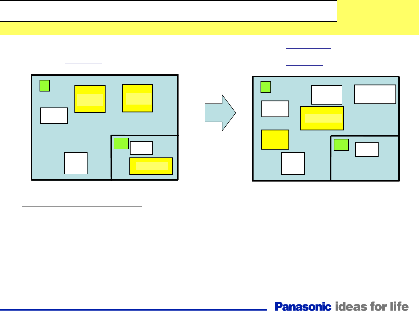
Chassis structure (37 Full HD type)
Chassis structure (37 Full HD type)
New
2007 Model (ex 37LZ700D) 2008 Model (ex 37LZ85 )
I
nv
e
r
t
e
r
Notice
A
P
LCD Panel
P
LCD Panel
A
P
H
D
G
I
nv
V
I
nv
e
r
t
e
r
e
r
t
e
r
H and DG boards are integrated to A board
V
I
nv
e
r
t
e
r
The H and DG board are integrated to A board of the 2008 model.
Therefore the Input switch, system control, and signal processing are performed by the A board.
The AP board is merged with the P board.
65
Page 66

Chassis structure (37 HD type)
Chassis structure (37 HD type)
New
2007 Model (ex 32LX70 series)
A
P
P
I
nv
V
e
r
t
e
r
I
nv
A
e
r
t
e
r
Notice
2008 Model (ex 32LX85 series)
LCD PanelLCD Panel
A
P
V
I
nv
e
r
t
e
r
I
nv
e
r
t
e
r
AP board is now merged with the P board
The A, P, and V boards are the only printed circuit boards used in the 2008 models.
66
Page 67

Signal Circuit Block Diagram
Signal Circuit Block Diagram
The A board is responsible for video input selection, video processing, and audio
processing. The LVDS output signal is provided to the LCD panel for display and the
audio signal to the speakers, headphone jack, and optical output jack.
67
Page 68

TC--
TC
32LX85 / TC37LZ85 Signal Circuit Block Diagram
32LX85 / TC37LZ85 Signal Circuit Block Diagram
The A board is responsible for video input selection, video processing, and
audio processing. The LVDS output signal is provided to the LCD panel for display and
the audio signal to the speakers, headphone jack, and optical output jack.
68
Page 69

TC37LZ85 Signal Circuit Block Diagram
TC37LZ85 Signal Circuit Block Diagram
69
Page 70

TC37LZ85 Signal Circuit Block Diagram
TC37LZ85 Signal Circuit Block Diagram
The main function of the A board is to select and process incoming video signals. Video inputs, Component
Video Input, and the composite video output of the tuner are all connected to IC3301 for selection. The video output signal of
the switch can be in any of the three analog formats: Video, Y/C, or Y, Pb, Pr. The selected output enters IC4510, the HDMI
IF Receiver/Decoder IC, for A/D conversion. The 10 bit YUV data is provided to a video switch. The HDMI receiver section of
IC4510 converts the incoming HDMI signals to YUV data and outputs to the switch. The output of the switch is provided to the
PEAKS LITE IC, IC8001.
Digital television reception of the tuner is output in the form of a transport stream (CHODATA). The transport
stream enters the DTV I/F (Interface) section of IC8001 where the video signal is extracted and converted to YUV data. The
JPEG data of the GS board enters the JPEG I/F section of IC8001 for conversion into YUV data. The internal video selector
of IC8001 (not shown in the diagram) selects and outputs the desired picture data to the Video Process circuit.
The Video Process section of the IC8001 performs all picture control operations such as brightness, contrast,
color, tint, etc. On Screen Display data such as channel numbers, Digital TV closed caption, and picture adjustments are
mixed with the video data. The output of IC8001 is provided to IC4202, the LVDS transmitter. The transmitter distributes
signals with low-jitter, while creating little noise. It reduces power consumption and the generated noise from data
transmission. Another benefit of the LVDS standard is minimal concern for cable length. The output of the LVDS transmitter is
provided to the LCD for display.
70
Page 71

TC32LX85 Signal Circuit Block Diagram
TC32LX85 Signal Circuit Block Diagram
71
Page 72

TC32LX85 Signal Circuit Block Diagram
TC32LX85 Signal Circuit Block Diagram
The main function of the A board is to select and process incoming video signals. The HDMI receiver located
inside IC4003 converts the HDMI signal into YUV data. Analog signals such as; Video inputs, component video Input,
composite video output of the tuner are all connected to IC4003 for selection. The selected analog signal enters the A/D
converter circuit for conversion into YUV data. An internal switch of IC4003 selects the desired signal and outputs to the
PEAKS LITE IC, IC8001.
Digital television reception of the tuner is output in the form of a transport stream (CHODATA). The transport
stream enters the DTV decoder section of IC8001 where the video signal is extracted and converted to YUV data. The JPEG
data of the GS board enters the SD/IF section of IC8001 for conversion into YUV data. The internal video selector of IC8001
(not shown in the diagram) selects and outputs the desired picture data to the Video Process circuit.
The Video Process section of the IC8001 performs all picture control operations such as brightness, contrast,
color, tint, etc. On Screen Display data such as channel numbers, Digital TV closed caption, and picture adjustments are
mixed with the video data. The RGB output of the video process section of the IC undergoes conversion to a LVDS signal
before being output to the LCD panel for display.
72
Page 73

TC37LZ85 Audio Circuit Block Diagram
TC37LZ85 Audio Circuit Block Diagram
73
Page 74

TC37LZ85 Audio Circuit Block Diagram
TC37LZ85 Audio Circuit Block Diagram
IC3301 of the A board handles the audio selection of most inputs. Analog audio of the tuner and audio signals
from composite, component, and DVI inputs are connected to IC3301 for selection. The output of IC3301 enters IC2106 and
undergoes analog to digital conversion.
IC4510 converts the incoming HDMI audio into serial data and outputs to IC2106. Digital television reception of
the tuner is output in the form of a transport stream that contains MPEG2 video and AC3 audio. The transport stream enters
the DTV decoder section of IC8001 where the audio signal is extracted and converted to serial data. The DTV audio data is
output to the audio DSP (Digital Signal Processor) IC2106 for processing.
The DSP IC2106 provides three audio outputs. One output is either AC3 or PWM audio connected to the digital
audio output jack. A second output is analog audio provided to the headphone jack. The third output is adjusted for volume,
bass, treble, and balance and then output as PWM data to the audio amplifier IC2301. The amplified two channel PWM data
is output to the right and left channel speakers for sound reproduction.
74
Page 75

TC32LX85 Audio Circuit Block Diagram
TC32LX85 Audio Circuit Block Diagram
75
Page 76

TC32LX85 Audio Circuit Block Diagram
TC32LX85 Audio Circuit Block Diagram
IC4003 of the A board handles the audio process of all inputs. Analog audio of the tuner and audio signals from
composite, component, and DVI inputs are connected to IC4003 for selection and process..
IC4503 converts the incoming HDMI audio into serial data and outputs to IC4003. Digital television reception of
the tuner is output in the form of a transport stream that contains MPEG2 video and AC3 audio. The transport stream enters
the DTV decoder section of IC8001 where the audio signal is extracted and converted to serial data. The DTV audio data is
then output to IC4003 for processing.
IC4003 provides three audio outputs. One output is either AC3 or PWM audio connected to the digital audio
output jack. A second output is analog audio provided to IC4002 for amplification and then the headphone jack. The third
output is adjusted for volume, bass, treble, and balance and then output as PWM data to the audio amplifier IC2301. The
amplified two channel PWM data is output to the right and left channel speakers for sound reproduction.
76
Page 77

Power Supply Overview
Power Supply Overview
77
Page 78

TC--
TC
37LZ85 Power Supply Description
37LZ85 Power Supply Description
78
Page 79

TC--
TC
37LZ85 Power Supply Description
37LZ85 Power Supply Description
When AC is applied to the TV, the Standby circuit of the P board outputs STB5V to the A board. On the A
board The STB5V is converted to 3.3V to power the system control circuit (not shown in the diagram) for standby operation.
The STB3.3V is also applied to the Remote Control receiver and the power LED on the V board. The MCU (IC1100) of the A
board outputs the SUB_ON command to provide a ground connection to relay RL802 of the power supply board. On the A
board, the SUB_ON command is used to turn on a switch that provides STB5V to relay RL802 via pin 13 of connector
A04/P6. When the relay is closed, 370Vdc from the PFC (Power Factor Control) is supplied to the LCD panel for conversion
into 120AC. The 370Vdc of the PFC is also provided to the switch mode power supply for conversion into Sub+9V, BT+30V,
DTV+12V, SUB+5V.
If the power button (main unit or remote control) is not pressed within 15 seconds after applying AC to the unit,
the SUB_ON command goes low to disengage the power relay. As a result, only STB+5V is output to power the system
control circuit of the a board.
When the power button is pressed, the SUB_ON command goes high to repeat the same operation. The
voltages remain present until the unit is turned off. The MCU also provides the Panel_ON command to trigger the output of
PANEL+12V. This voltage is used to turn on the inverter PCBs for the production of 120VAC used to illuminate the backlights
of the LCD panel. The PANEL+12V is also used to operate the drive circuits of the LCD panel. The MCU also outputs the
Main_ON command to trigger the output of the SOUND+17V source.
When the power supply output is too high, an over-voltage detection circuit outputs a high to the A board to
trigger the shutdown of the unit. The power LED does not blink.
An over-current detection circuit on the power supply board monitors for short circuits. If a detection is made, a
high is output to IC1100 to shut down the unit and provide 3 blinks of the power LED.
Caution: The P board is to be exchanged only.
79
Page 80

Self--
Self
Check and Reset Function
Check and Reset Function
80
Page 81

SOS and Power LED Indication
SOS and Power LED Indication
81
Page 82

Power LED Blinks 1 Time
Power LED Blinks 1 Time
Pin 4 of connector P2 should toggle low after the backlights of the LCD panel turn on. If the backlights
do not come on or pin 4 of CN P2 does not toggle low, Reseat the connectors A4, P6, and P2. Confirm the presence
of 370Vdc at pin 1 of connector P5 and 12V at pin 1 of connector P2 before replacing the LCD panel.
82
Page 83

Power LED Blinks 3 Times
Power LED Blinks 3 Times
Pin 10 of connector P7/A3 outputs a high when an over-current condition is detected. On the power
supply board, locate the test points for the SUB9V, SOUND17V and BT30V. Using an ohmmeter, determine if there
is a short between each of the test-point and ground. If a test-point is shorted, disconnect the connector P7 or A3 to
isolate the short to either the A or P board.
83
Page 84

Power LED Blinks 4 or 5 Times
Power LED Blinks 4 or 5 Times
The DTV12V and SUB9V lines are monitored by the MCU. If the voltage corresponding to the number
of blinks is missing or shorted, the MCU shuts down the unit and blinks the Power LED. Reseat the connectors P7
and A3 and turn on the unit. If the shutdown persists, use a voltmeter to measure the voltage. If it is present, replace
the A board. If it is absent, use an ohmmeter to determine if there is a short to ground. When a short is detected,
disconnect the connector P7 or A3 to isolate the short to either the A or P board.
84
Page 85

Power LED Blinks 6 or 7 Times
Power LED Blinks 6 or 7 Times
The SUB5V and SUB3.3V lines are monitored by the MCU. When the SUB5V is missing or shorted, the
MCU shuts down the unit and blinks the Power LED. Reseat the connectors P7 and A3 and turn on the unit. If the
shutdown persists, use a voltmeter to measure the voltage. If it is present, replace the A board. If it is absent, use an
ohmmeter to determine if there is a short to ground. When a short is detected, disconnect the connector P7 or A3 to
narrow it to the A or P board. A seven-blinks shutdown is always caused by the A board.
85
Page 86

Power LED Blinks 8 or 9 Times
Power LED Blinks 8 or 9 Times
On the A board, the MCU (IC1100) monitors the SOUND+17V line and the operation of the audio power
amplifier IC2301. If IC2301, or the 17V lines develops a short to ground, a high is provided to the MCU to trigger a SOS
condition. The power LED blinks 9 times.
Use a voltmeter to measure the SOUND+17V source. If it is present, replace the A board. If it is absent, use
an ohmmeter to determine if there is a short to ground. When a short is detected, disconnect the connector P7 or A3 to
narrow it to the A or P board. A eight-blinks shutdown is always caused by the A board.
86
Page 87

Power LED Blinks 1 Time (TC--
Power LED Blinks 1 Time (TC
32LX85)
32LX85)
Pin 5 of connector A16 should toggle low after the backlights of the LCD panel turn on. If the backlights
do not come on or pin 5 of CN A16 does not toggle low, Reseat the connectors A3, P3, and P7. Confirm the
presence of 24Vdc at pin 1 of connector P7 and 12V at pin 28 of connector A2 before replacing the LCD panel.
87
Page 88

Power LED Blinks 3 Times (TC--
Power LED Blinks 3 Times (TC
32LX85)
32LX85)
Pin 10 of connector P3/A3 outputs a high when an over-current condition is detected. On the power
supply board, locate the test points for the SUB9V, SOUND15V, BT30V, and PANEL12V. Using an ohmmeter,
determine if there is a short between each of the test-point and ground. If a test-point is shorted, disconnect the
connector P3 or A3 to isolate the short to either the A or P board.
88
Page 89

Power LED Blinks 4 or 5 Times (TC--
Power LED Blinks 4 or 5 Times (TC
32LX85)
32LX85)
The DTV12V and SUB9V lines are monitored by the MCU. If the voltage corresponding to the number
of blinks is missing or shorted, the MCU shuts down the unit and blinks the Power LED. Reseat the connectors P3
and A3 and turn on the unit. If the shutdown persists, use a voltmeter to measure the voltage. If it is present, replace
the A board. If it is absent, use an ohmmeter to determine if there is a short to ground. When a short is detected,
disconnect the connector P3 or A3 to isolate the short to either the A or P board.
89
Page 90

Power LED Blinks 6 or 7 Times (TC--
Power LED Blinks 6 or 7 Times (TC
32LX85)
32LX85)
The SUB5V and SUB3.3V lines are monitored by the MCU. When the SUB5V is missing or shorted, the
MCU shuts down the unit and blinks the Power LED. Reseat the connectors P7 and A3 and turn on the unit. If the
shutdown persists, use a voltmeter to measure the voltage. If it is present, replace the A board. If it is absent, use an
ohmmeter to determine if there is a short to ground. When a short is detected, disconnect the connector P7 or A3 to
narrow it to the A or P board. A seven-blinks shutdown is always caused by the A board.
90
Page 91

Power LED Blinks 8 or 9 Times (TC--
Power LED Blinks 8 or 9 Times (TC
32LX85)
32LX85)
On the A board, the MCU (IC4003) monitors the SOUND+17V line and the operation of the audio power
amplifier IC2301. If IC2301, or the 15V lines develops a short to ground, a high is provided to the MCU to trigger a SOS
condition. The power LED blinks 9 times.
Use a voltmeter to measure the SOUND+15V source. If it is present, replace the A board. If it is absent, use
an ohmmeter to determine if there is a short to ground. When a short is detected, disconnect the connector P3 or A3 to
narrow it to the A or P board. A eight-blinks shutdown is always caused by the A board.
91
Page 92

Picture Defect (1)
Picture Defect (1)
Trouble
Where is
the abnormal picture
displayed ?
Upper or Lower
Left or Right
Vertical or Horizontal line
(1)Part of the screen
Upper
Panel
Lower
Panel
Right
Panel
Left
Panel
Panel
(2)All over the screen
All over the screen
(3)No picture
Many vertical lines
Non-uniformity color
92
Abnormal color
Panel
OSD trouble
A Board
Page 93

Picture Defect (2)
Picture Defect (2)
<Symptom>Upper or Lower Defect
Abnormality means
No Picture, Picture noise, abnormal picture,
Full Horizontal line etc.
<NG Area>
Panel Drive Panel Drive
Panel
Drive
Panel
Drive
Panel
Drive
<Actual Symptom>
Symptom: Upper trouble
A
Tuner
Input
Terminal
Signal
Processor
<Defective parts>
Panel (Panel drive)
Relation to panel drive location,
1/3 or 2/3 area will be troubled.
LCD panel
93
Page 94

Picture Defect (3)
Picture Defect (3)
<Symptom>Left or Right half defect
No Picture, Picture noise, Full Horizontal line, etc.
<NG Area>
Panel Drive Panel Drive
Panel
Drive
Panel
Drive
Panel
Drive
<Actual Symptom>
Symptom: Right half picture trouble
A
Tuner
Input
Terminal
Signal
Processor
LCD panel
<Defective parts>
Panel (Panel drive) or A board
94
Page 95

Picture Defect (4)
Picture Defect (4)
<Symptom>Horizontal line
<NG Area>
Panel Drive Panel Drive
Panel
Drive
Panel
Drive
Panel
Drive
<Actual Symptom>
Symptom: Horizontal line
A
Tuner
Input
Terminal
Signal
Processor
LCD panel
<Defective parts>
Panel
95
Page 96

Picture Defect (5)
Picture Defect (5)
<Symptom>Vertical line
<NG Area>
Panel Drive Panel Drive
Panel
Drive
Panel
Drive
Panel
Drive
<Actual Symptom>
Symptom: Thin vertical line
A
Tuner
Input
Terminal
Signal
Processor
LCD panel
<Defective parts>
Panel
96
Page 97

Picture Defect (6)
Picture Defect (6)
<Symptom>Vertical line noise
<NG Area>
Panel Drive Panel Drive
Vertical noise
LCD panel
Panel
Drive
Panel
Drive
Panel
Drive
<Actual Symptom>
Symptom: Vertical noise
A
Tuner
Input
Terminal
Signal
Processor
<Defective parts>
Panel or A board
97
Page 98

Picture Defect (7)
Picture Defect (7)
<Symptom>Sub picture NG
<NG Area>
<Actual Symptom>
<Actual Symptom>
Symptom: Sub picture NG
Panel Drive Panel Drive
LCD panel
<Defective parts>
A board
Panel
Drive
Panel
Drive
Panel
Drive
A
Tuner
Input
Terminal
Signal
Processor
Note:
There is not sub picture function
on some models.
98
Page 99

Picture Defect (8)
Picture Defect (8)
<Symptom>Non uniformity color
<NG Area>
Panel Drive Panel Drive
Panel
Drive
Panel
Drive
Panel
Drive
<Actual Symptom>
Symptom: Irregular color
A
Tuner
Input
Terminal
Signal
Processor
LCD panel
<Defective parts>
Panel
99
Page 100

Picture Defect (9)
Picture Defect (9)
<Symptom>Vertical lines all over screen
<NG Area>
Panel Drive Panel Drive
Panel
Drive
Panel
Drive
Panel
Drive
LCD panel
Tuner
Input
Terminal
Signal
Processor
<Actual Symptom>
Symptom: Vertical line all over screen
A
<Defective parts>
Mainly A board, in some cases panel
100
 Loading...