

Page 1
ORDER NO.PAVCTH1203002CE
Plasma Television
Model No. TH-P50ST50A
TH-P50ST50D
TH-P50ST50G
TH-P50ST50K
TH-P50ST50M
TH-P50ST50P
TH-P50ST50S
TH-P50ST50T
TH-P50ST50V
TH-P50ST50Z
GPF15D-A Chassis
© Panasonic Corporation 2012.
Unauthorized copying and distribution is a violation
of law.
Page 2

TABLE OF CONTENTS
PAG E
1 Safety Precautions -----------------------------------------------3
1.1. General Guidelines ----------------------------------------3
1.2. Touch-Current Check--------------------------------------3
2Warning--------------------------------------------------------------4
2.1. Prevention of Electrostatic Discharge (ESD)
to Electrostatically Sensitive (ES) Devices ----------4
2.2. About lead free solder (PbF) ----------------------------5
3 Service Navigation------------------------------------------------6
3.1. PCB Layout --------------------------------------------------6
3.2. Applicable signals ------------------------------------------7
4 Specifications ------------------------------------------------------8
5 Technical Descriptions---------------------------------------- 10
5.1. Specification of KEY for DTCP-IP, One-toOne, Widevine and Netflix ----------------------------- 10
5.2. USB HDD Recording (A/Z only) ---------------------- 10
5.3. Panel-Type setting --------------------------------------- 10
6 Service Mode ----------------------------------------------------- 11
6.1. How to enter into Service Mode ---------------------- 11
6.2. Option - Mirror--------------------------------------------- 13
6.3. Service tool mode ---------------------------------------- 13
6.4. DRV Check - USB HDD Check----------------------- 14
6.5. Hotel mode------------------------------------------------- 14
6.6. Data Copy by SD Card --------------------------------- 15
7 Troubleshooting Guide---------------------------------------- 18
7.1. Check of the IIC bus lines------------------------------ 18
7.2. Power LED Blinking timing chart --------------------- 19
7.3. No Power--------------------------------------------------- 20
7.4. No Picture -------------------------------------------------- 21
7.5. Local screen failure -------------------------------------- 22
8 Service Fixture & Tools --------------------------------------- 23
8.1. SC jig -------------------------------------------------------- 23
9 Disassembly and Assembly Instructions --------------- 24
9.1. Disassembly Flow Chart for the Unit ---------------- 24
9.2. Disassembly Procedure for the Unit----------------- 25
10 Measurements and Adjustments -------------------------- 32
10.1. Adjustment ------------------------------------------------- 32
11 Block Diag ram ---------------------------------------------------35
11.1. Main Block Diagram ------------------------------------- 35
11.2. Block (1/4) Diagram ------------------------------------- 36
11.3. Block (2/4) Diagram ------------------------------------- 37
11.4. Block (3/4) Diagram ------------------------------------- 38
11.5. Block (4/4) Diagram ------------------------------------- 39
12 Wiring Connection Diagram --------------------------------- 41
12.1. Caution statement.--------------------------------------- 41
12.2. Wiring (1) --------------------------------------------------- 41
12.3. Wiring (2) --------------------------------------------------- 42
12.4. Wiring (3) --------------------------------------------------- 42
13 Schematic Diagram
14 Printed Circuit Board
15 Exploded View
2
Page 3
1 Safety Precautions
1.1. General Guidelines
1. When conducting repairs and servicing, do not attempt to modify the equipment, its parts or its materials.
2. When wiring units (with cables, flexible cables or lead wires) are supplied as repair parts and only one wire or some of the
wires have been broken or disconnected, do not attempt to repair or re-wire the units. Replace the entire wiring unit instead.
3. When conducting repairs and servicing, do not twist the Fasten connectors but plug them straight in or unplug them straight
out.
4. When servicing, observe the original lead dress. If a short circuit is found, replace all parts which have been overheated or
damaged by the short circuit.
5. After servicing, see to it that all the protective devices such as insulation barriers, insulation papers shields are properly
installed.
6. After servicing, make the following leakage current checks to prevent the customer from being exposed to shock hazards.
1.2. Touch-Current Check
1. Plug the AC cord directly into the AC outlet. Do not use an isolation transformer for this check.
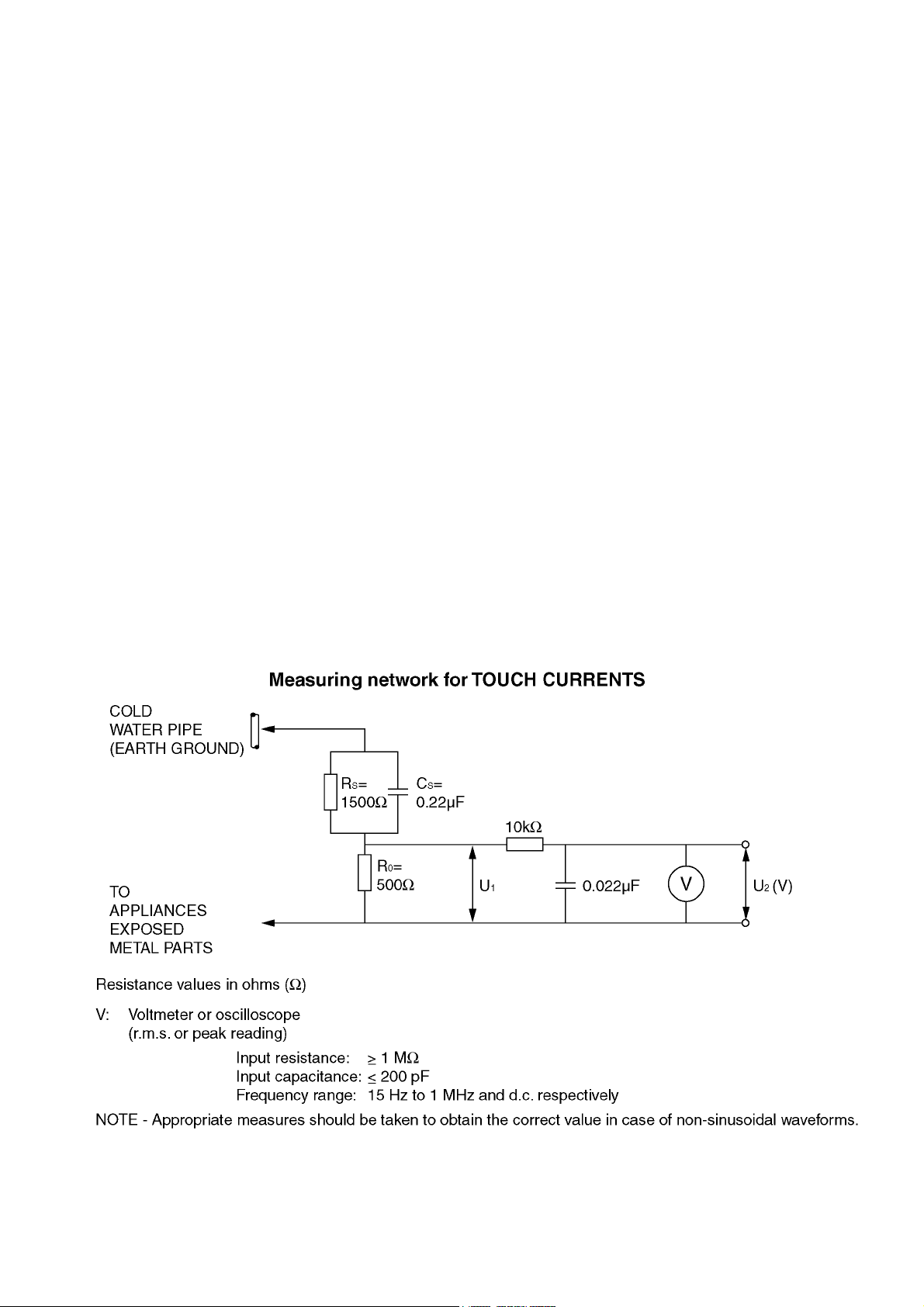
2. Connect a measuring network for touch currents between each exposed metallic part on the set and a good earth ground
such as a water pipe, as shown in Figure 1.
3. Use Leakage Current Tester (Simpson 228 or equivalent) to measure the potential across the measuring network.
4. Check each exposed metallic part, and measure the voltage at each point.
5. Reserve the AC plug in the AC outlet and repeat each of the above measure.
6. The potential at any point (TOUCH CURRENT) expressed as voltage U
For a. c.: U1 = 35 V (peak) and U2 = 0.35 V (peak);
For d. c.: U
Note:
The limit value of U
mA d. c.
The limit value U
7. In case a measurement is out of the limits specified, there is a possibility of a shock hazard, and the equipment should be
repaired and rechecked before it is returned to the customer.
= 1.0 V,
1
= 0.35 V (peak) for a. c. and U1 = 1.0 V for d. c. correspond to the values 0.7 mA (peak) a. c. and 2.0
2
= 35 V (peak) for a. c. correspond to the value 70 mA (peak) a. c. for frequencies greater than 100 kHz.
1
and U2, does not exceed the following values:
1
Figure 1
3
Page 4

2Warning
2.1. Prevention of Electrostatic Discharge (ESD) to Electrostatically Sensitive (ES) Devices
Some semiconductor (solid state) devices can be damaged easily by static electricity. Such components commonly are called
Electrostatically Sensitive (ES) Devices. Examples of typical ES devices are integrated circuits and some field-effect transistors and
semiconductor [chip] components. The following techniques should be used to help reduce the incidence of component damage
caused by electrostatic discharge (ESD).
1. Immediately before handling any semiconductor component or semiconductor-equipped assembly, drain off any ESD on your
body by touching a known earth ground. Alternatively, obtain and wear a commercially available discharging ESD wrist strap,
which should be removed for potential shock reasons prior to applying power to the unit under test.
2. After removing an electrical assembly equipped with ES devices, place the assembly on a conductive surface such as
aluminum foil, to prevent electrostatic charge buildup or exposure of the assembly.
3. Use only a grounded-tip soldering iron to solder or unsolder ES devices.
4. Use only an anti-static solder removal device. Some solder removal devices not classified as [anti-static (ESD protected)] can
generate electrical charge sufficient to damage ES devices.
5. Do not use freon-propelled chemicals. These can generate electrical charges sufficient to damage ES devices.
6. Do not remove a replacement ES device from its protective package until immediately before you are ready to install it. (Most
replacement ES devices are packaged with leads electrically shorted together by conductive foam, aluminum foil or
comparable conductive material).
7. Immediately before removing the protective material from the leads of a replacement ES device, touch the protective material
to the chassis or circuit assembly into which the device will be installed.
Caution
Be sure no power is applied to the chassis or circuit, and observe all other safety precautions.
8. Minimize bodily motions when handling unpackaged replacement ES devices. (Otherwise ham less motion such as the
brushing together of your clothes fabric or the lifting of your foot from a carpeted floor can generate static electricity (ESD)
sufficient to damage an ES device).
4
Page 5
2.2. About lead free solder (PbF)
Note: Lead is listed as (Pb) in the periodic table of elements.
In the information below, Pb will refer to Lead solder, and PbF will refer to Lead Free Solder.
The Lead Free Solder used in our manufacturing process and discussed below is (Sn+Ag+Cu).
That is Tin (Sn), Silver (Ag) and Copper (Cu) although other types are available.
This model uses Pb Free solder in it's manufacture due to environmental conservation issues. For service and repair work, we'd
suggest the use of Pb free solder as well, although Pb solder may be used.
PCBs manufactured using lead free solder will have the PbF within a leaf Symbol PbF stamped on the back of PCB.
Caution
• Pb free solder has a higher melting point than standard solder. Typically the melting point is 50 ~ 70 °F (30~40 °C) higher. Please
use a high temperature soldering iron and set it to 700 ± 20 °F (370 ± 10 °C).
• Pb free solder will tend to splash when heated too high (about 1100 °F or 600 °C).
If you must use Pb solder, please completely remove all of the Pb free solder on the pins or solder area before applying Pb
solder. If this is not practical, be sure to heat the Pb free solder until it melts, before applying Pb solder.
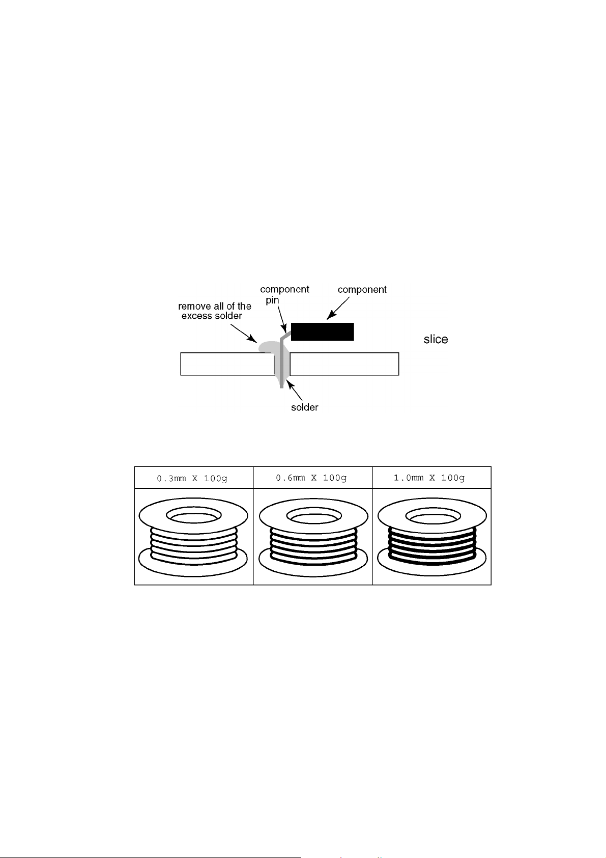
• After applying PbF solder to double layered boards, please check the component side for excess solder which may flow onto the
opposite side. (see figure below)
Suggested Pb free solder
There are several kinds of Pb free solder available for purchase. This product uses Sn+Ag+Cu (tin, silver, copper) solder.
However, Sn+Cu (tin, copper), Sn+Zn+Bi (tin, zinc, bismuth) solder can also be used.
5
Page 6
3 Service Navigation
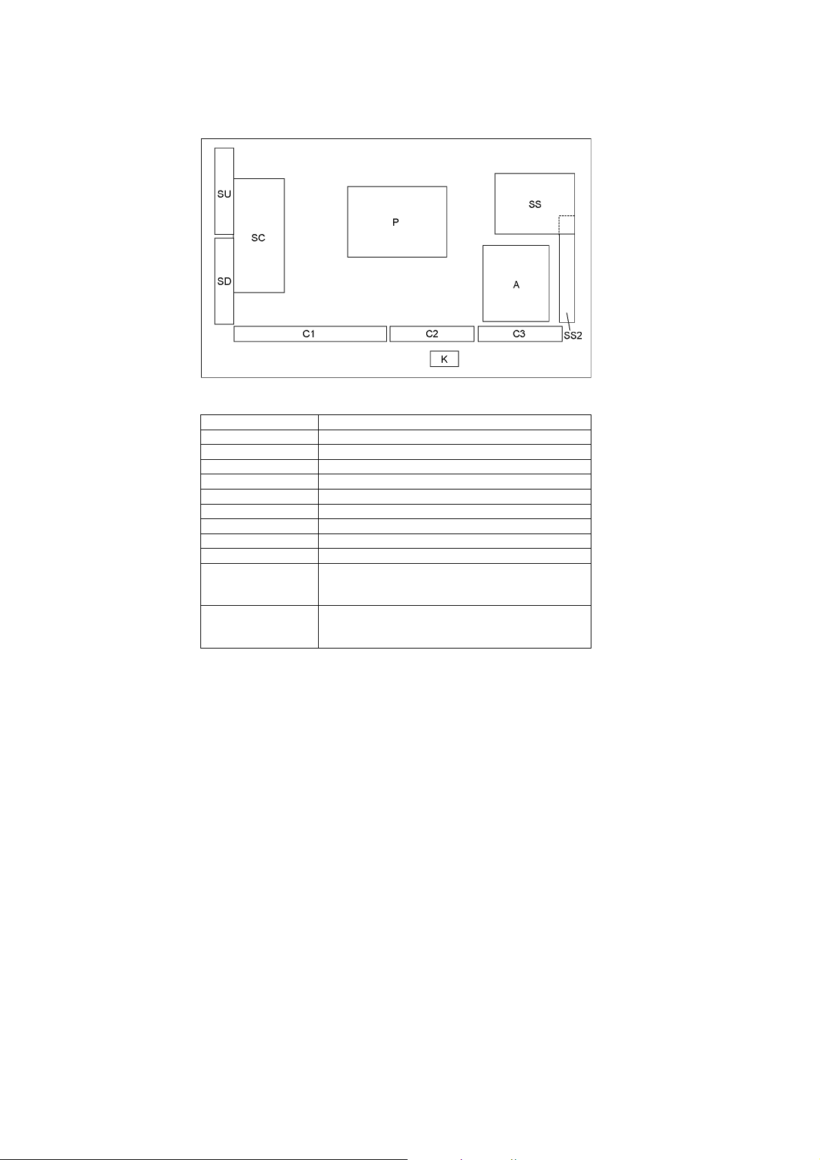
3.1. PCB Layout
Board Name Function
P Power Supply
A Main AV input, processing
K Remote receiver, Power LED, C.A.T.S sensor
C1 Data Driver (Lower Right)
C2 Data Driver (Lower Center)
C3 Data Driver (Lower Left)
SC Scan Drive
SS Sustain Drive
SS2 Sustain out (Lower)
SU Scan out (Upper)
SD Scan out (Lower)
Non serviceable.
SU-Board should be exchanged for service.
Non serviceable.
SD-Board should be exchanged for service.
6
Page 7
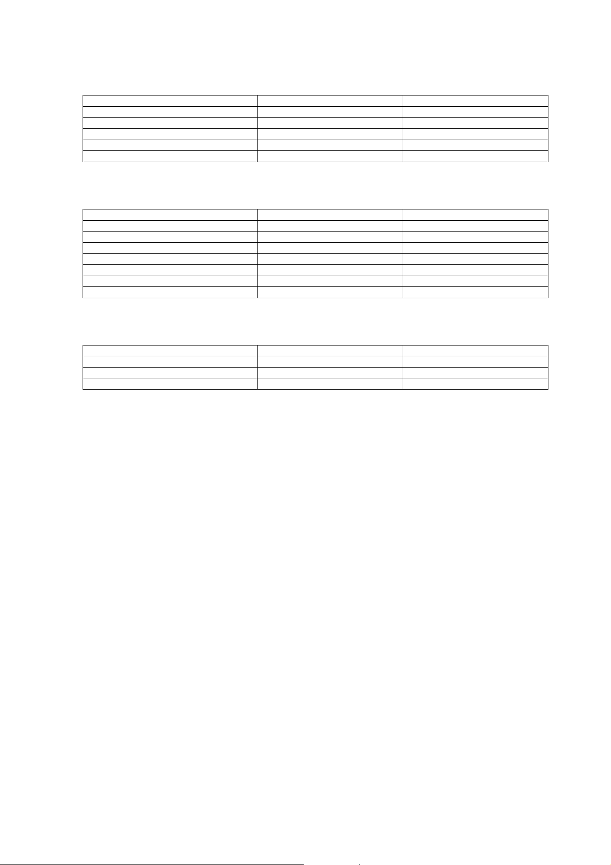
3.2. Applicable signals
Q COMPONENT (Y, PB, PR) (from AV2 terminal), HDMI
Signal name COMPONENT HDMI
525 (480) / 60i, 60p * *
625 (576) / 50i, 50p * *
750 (720) / 60p, 50p * *
1,125 (1,080) / 60i, 50i * *
1,125 (1,080) / 60p, 50p, 24p *
* Mark: Applicable input signal
Q PC (from D-sub 15P)
Signal name Horizontal frequency (kHz) Vertical frequency (Hz)
640 × 480 @60 Hz 31.47 59.94
800 × 600 @60 Hz 37.88 60.32
852 × 480 @60 Hz 31.44 59.89
1,024 × 768 @60 Hz 48.36 60.00
1,280 × 1,024 @60 Hz 63.98 60.02
1,280 × 768 @60 Hz 47.70 60.00
1,366 × 768 @60 Hz 48.39 60.04
Applicable input signal for PC is basically compatible to VESA standard timing.
Q PC (from HDMI terminal)
Signal name Horizontal frequency (kHz) Vertical frequency (Hz)
640 × 480 @60 Hz 31.47 60.00
1,280 × 720 @60 Hz 45.00 60.00
1,920 × 1,080 @60 Hz 67.50 60.00
Applicable input signal for PC is basically compatible to HDMI standard timing.
Note
• Signals other than above may not be displayed properly.
• The above signals are reformatted for optimal viewing on your display.
• PC signal is magnified or compressed for display, so that it may not show fine detail with sufficient clarity.
7
Page 8
4 Specifications
Power (A/Z)
Power rating AC 220-240 V, 50 / 60 Hz 2.4 A
Normal (Home) mode 137 W
Standby condition 0.4 W
Power Source (Except A/Z) AC 220 - 240 V, 50 / 60 Hz (Except P)
AC 110 - 240 V, 50 / 60 Hz (P)
Power Consumption (Except A/Z)
Power Rating 420 W (Except P) 425 W (P)
Standby condition 0.4 W
Display panel
Panel system Plasma panel
Visible screen size (diagonal) 127 cm / 50 inches
Number of pixels 2,073,600 (1,920 (W) × 1,080 (H)), [5,760 × 1,080 dots]
Dimensions (W × H × D) 1,180 mm × 757 mm × 335 mm (With Pedestal)
1,180 mm × 709 mm × 50 mm (TV only)
Mass 27.0 kg Net (With Pedestal)
Sound
Speaker
Audio output 18 W (4 W + 4 W + 10 W)
Headphones M3 (3.5 mm) stereo mini Jack × 1
Receiving systems / Band name (A/Z)
PAL B / G Reception of Off air broadcasts
Digital TV 7 MHz VHF/UHF (Australia) free-to-air TV broadcast reception (A)
PAL 60 Hz Playback of NTSC tape from some PAL Video recorders (VCR)
M.NTSC Playback from M.NTSC Video recorders (VCR)
NTSC Playback from NTSC Video recorders (VCR)
Receiving systems / Band name (Except
A/Z)
23.0 kg Net (TV only)
Front speaker (8 train speakers) × 2, Woofer ( 80 mm) × 1
8 MHz UHF (New Zealand) free-to-air TV broadcast reception (Z)
Receiving Channels (Except A/Z)
VHF BAND
2-12 (PAL/SECAM B, K1) 0-12 (PAL B AUST.)
1-9 (PAL B N.Z.) 1-12 (PAL/SECAM D)
1-12 (NTSC M Japan) 2-13 (NTSC M USA)
UHF BAND
21-69 (PAL G, H, I/SECAM G, K, K1)
28-69 (PAL B AUST.) 13-57 (PAL D, K)
13-62 (NTSC M Japan) 14-69 (NTSC M USA)
CATV
S1-S20 (OSCAR) 1-125 (USA CATV)
C13-C49 (JAPAN) S21-S41 (HYPER)
Z1-Z37 (CHINA) 5A, 9A (AUST.)
Aerial - Rear Standard Belling & Lee connector (A)
VHF / UHF (Except A)
Operating Conditions
Temperature: 0 °C - 40 °C (Except A/Z) 0 °C - 35 °C (A/Z)
Humidity: 20 % - 80 % RH (non-condensing)
Connection terminals
AV1 I N
AUDIO L - R RCA PIN Type × 2 0.5 V [rms]
VIDEO RCA PIN Type × 1 1.0 V [p-p] (75 Ω)
AUDIO OUT
DIO L - R RCA PIN Type × 2 0.5 V [rms] (high impedance)
AU
AV2 I N
AUDIO L - R RCA PIN Type × 2 0.5 V [rms]
COMPONENT Y 1.0 V [p-p] (including synchronization)
8
Page 9

PB/CB, PR/C
R
± 0.35 V [p-p]
VIDEO RCA PIN Type × 1 1.0 V [p-p] (75 Ω)
HDMI 1 / 2 / 3 input TYPE A Connectors
• This TV supports "HDAVI control 5" function.
PC HIGH-DENSITY D-SUB 15PIN
R,G, B: 0.7 V [p-p] (75 Ω)
HD, VD: TTL Level 2.0 - 5.0 V [p-p] (high impedance)
• Applicable input signals: VGA, SVGA, WVGA, XGA
SXGA, WXGA ...... (compressed)
Horizontal scanning frequency 31 - 69 kHz
Vertical scanning frequency 59 - 86 Hz
Card slot SD Card slot × 1
ETHERNET 10BASE-T / 100BASE-TX
USB 1 / 2 USB 2.0 TYPE A Connectors DC 5 V, Max. 500 mA
DIGITAL AUDIO OUT PCM / Dolby Digital / DTS, Fibre optic
Built-in wireless LAN
Standard compliance and
Frequency range*
1
IEEE 802.11a/n
5.15 GHz - 5.35 GHz, 5.47 GHz - 5.85 GHz
IEEE 802.11b/g/n
2.40 GHz - 2.4835 GHz
Security WPA2-PSK (TKIP/AES) WPA-PSK (TKIP/AES) WEP (64 bit/128 bit)
Bluetooth wireless technology*
2
Standard Compliance Bluetooth 3.0
Frequency Range 2.402 GHz - 2.480 GHz
1
*
: The frequency and channel differ depending on the country.
2
*
: Not all the Bluetooth compatible devices are available with this TV.
Q 3D Eyewear
Dimensions (W × H × D) 167.7 mm × 42.2 mm × 170.7 mm
Mass Approx. 31 g
Lens type Liquid Crystal Shutter
Usage temperature range 0 °C - 40 °C
Battery* Coin-shaped lithium battery CR2025
Operation time: Approx. 75 hours in continuous use of the battery made by Panasonic
Viewing range* Within 3.2 m from front surface of the TV
Materials Main body: Resin
Lens section: Liquid crystal glass
Communication system 2.4 GHz band FH-SS (Frequency Hopping Spread Spectrum)
* There are differences in the viewing range of the 3D Eyewear among individuals.
• The 3D Eyewear may not operate correctly at the outside of the viewing range.
Note
• Design and Specifications are subject to change without notice. Mass and Dimensions shown are approximate.
9
Page 10
5 Technical Descriptions
5.1. Specification of KEY for DTCP-IP, One-to-One, Widevine and Netflix
5.1.1. General information:
1. EEPROM (IC8902) for spare parts has the seed of KEY for each.
2. The final KEY data will be generated by Peaks IC (IC8000) when SELF CHECK was done and are stored in both Peaks IC
(IC8000) and EEPROM (IC8902).
Four KEY are not generated for all models.
The necessary KEY are only generated and stored depend on the feature of models.
5.1.2. Replacement of ICs:
When Peaks IC (IC8000) is replaced, EEPROM (IC8902) should be also replaced with new one the same time.
When EEPROM (IC8902) is replaced, Peaks IC (IC8000) is not necessary to be replaced the same time.
After the replacement of IC, SELF CHECK should be done to generate the final KEY data.
How to SELF CHECK: While pressing [VOLUME ( - )] button on the main unit, press [MENU] button on the remote control for more
than 3 seconds.
TV will be forced to the factory shipment setting after this SELF CHECK.
5.1.3. Model and Keys:
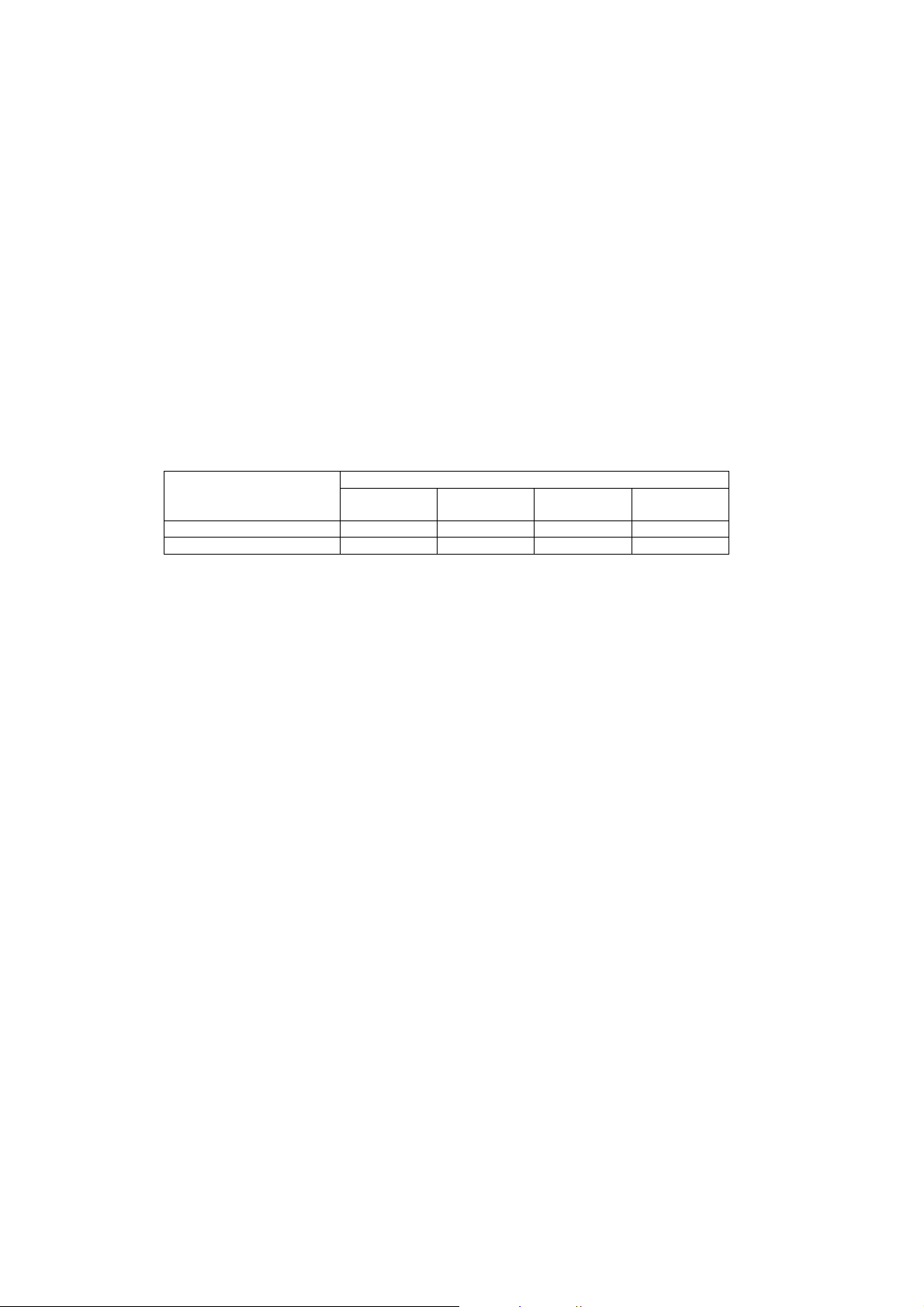
Model No. Keys
One-to-One
(For USB Rec.)
TH-P50ST50D/G/K/M/P/S/T/V None None Yes Yes
TH-P50ST50A/Z Yes Yes Yes Yes
DTCP-IP WIDEVINE Netflix
5.2. USB HDD Recording (A/Z only)
5.2.1. General information:
Digital TV programmes can be recorded in USB HDD.
A One-to-One key generated in A-board by SELF CHECK binds TV and USB-HDD for communication.
That key is only one key for them. If the key is difference, TV can not access USB-HDD.
Caution:
New key will be generated by following SELF CHECK and previous TV programmes recorded in USB HDD will not be
viewed.
SELF CHECK: While pressing [VOLUME ( - )] button on the main unit, press [MENU] button on the remote control for
more than 3 seconds.
5.3. Panel-Type setting
Panel-Type setting is required after exchange the A-board.
A-board for spare parts is common use for different inch size in same series.
Go into Service Mode and confirm/select Panel-Type in OPTION to correct inch size.
10
Page 11
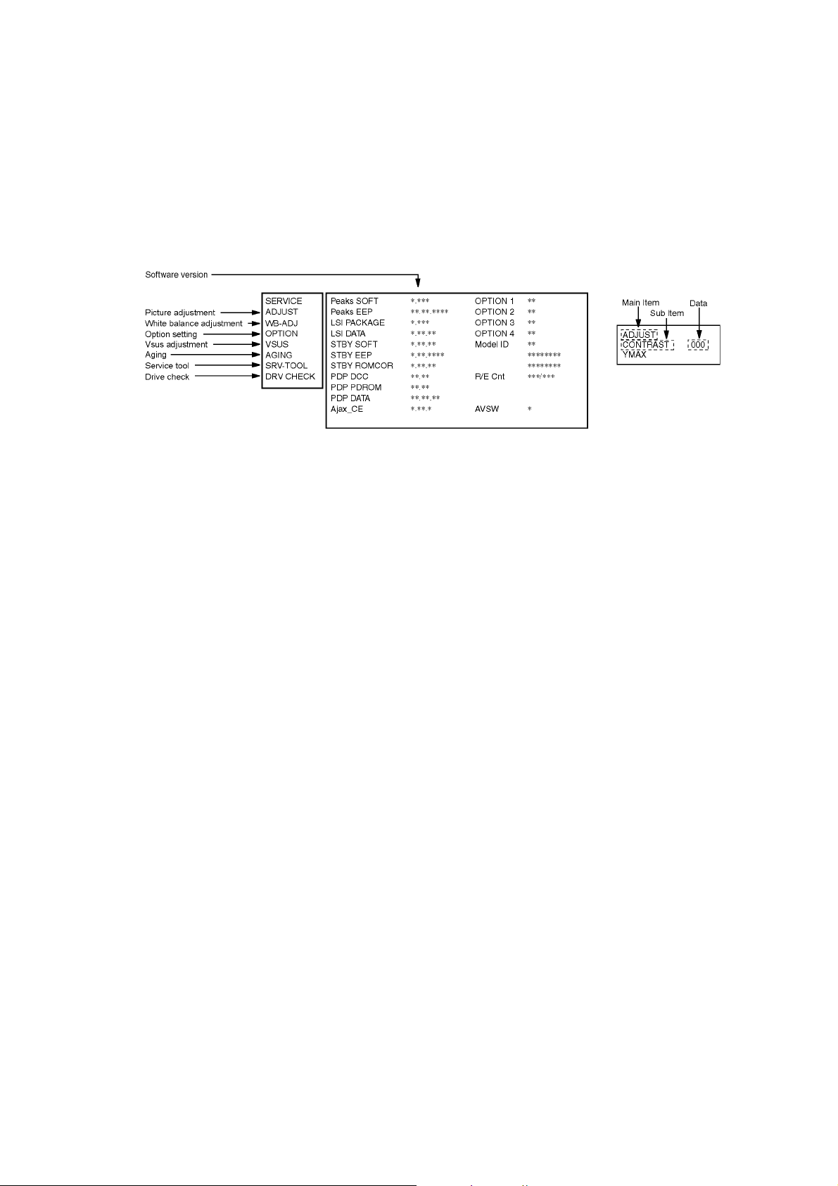
6 Service Mode
6.1. How to enter into Service Mode
6.1.1. Purpose
After exchange parts, check and adjust the contents of adjustment mode.
While pressing [VOLUME ( - )] button of the main unit, press [i] button of the remote control three times within 2 seconds.
Note:
Service Mode can not be entered when 3D signal input.
Input 2D signal to enter Service Mode.
6.1.2. Key command
[1] button...Main items Selection in forward direction
[2] button...Main items Selection in reverse direction
[3] button...Sub items Selection in forward direction
[4] button...Sub items Selection in reverse direction
[RED] button...All Sub items Selection in reverse direction
[GREEN] button...All Sub items Selection in forward direction
[VOL] button...Value of sub items change in forward direction ( + ), in reverse direction ( - )
6.1.3. How to exit
Switch off the power with the [POWER] button on the main unit or the [POWER] button on the remote control.
11
Page 12
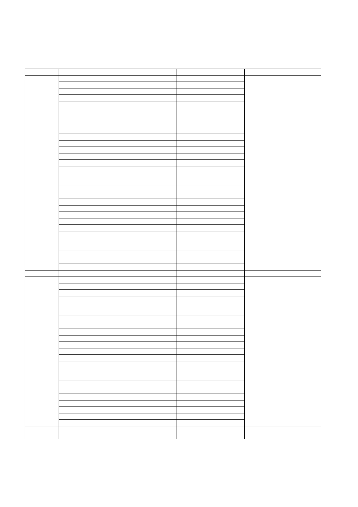
6.1.4. Contents of adjustment mode
• Value is shown as a hexadecimal number.
• Preset value differs depending on models.
• After entering the adjustment mode, take note of the value in each item before starting adjustment.
Main item Sub item Sample Data Remark
ADJUST CONTRAST 000
COLOR 3D
TINT 00
SUB-BRT 800
H-POS 0
H-AMP 0
V-POS 0
V-AMP 0
WB-ADJ R-CUT 80
G-CUT 80
B-CUT 80
R-DRV FF
G-DRV E7
B-DRV A5
ALL-CUT 80
ALL-DRV FF
OPTION Panel-Type 50FHD Factory Preset
Boot ROM
STBY-SET 00
EMERGENCY ON
CLK MODE 00
CLOCK 000
Y/C Delay
OPT 1 10110000
OPT 2 00100010
OPT 3 00000001
OPT 4 00010000
EDID-CLK MID
MIRROR 00 (See Option-Mirror)
AMR-SELECT OFF
VSUS LOW See Vsus selection
AGING ALL WHITE Built-in test patterns can be
MIDDLE BLUE WITH MAGENTA OUTSIDE FRAME
MIDDLE STEP GREEN
MIDDLE STEP RED
LOW STEP WHITE
ALL BLUE
ALL GREEN
ALL RED
WHITE DIAGONAL STRIPE
RED DIAGONAL STRIPE
GREEN DIAGONAL STRIPE
BLUE DIAGONAL STRIPE
A-ZONE & B-ZONE
1% WINDOW
COLOR BAR
9 POINTS BRIGHT MEASURE
2 DOT OUTSIDE FRAME
DOUBLE FIXED 1% WINDOW
VERTICAL LINE SCROLL
ON/OFF
R/G/B/W ROTATION WITH COUNT DISPLAY
HALF FIXED ALL WHITE
ALL WHITE WITH COUNT DISPLAY
SRV-TOOL 00 See Service tool mode
DRV CHECK USBHDD CHECK 00 See DRV Check-USBHDD Check
displayed.
12
Page 13
6.2. Option - Mirror
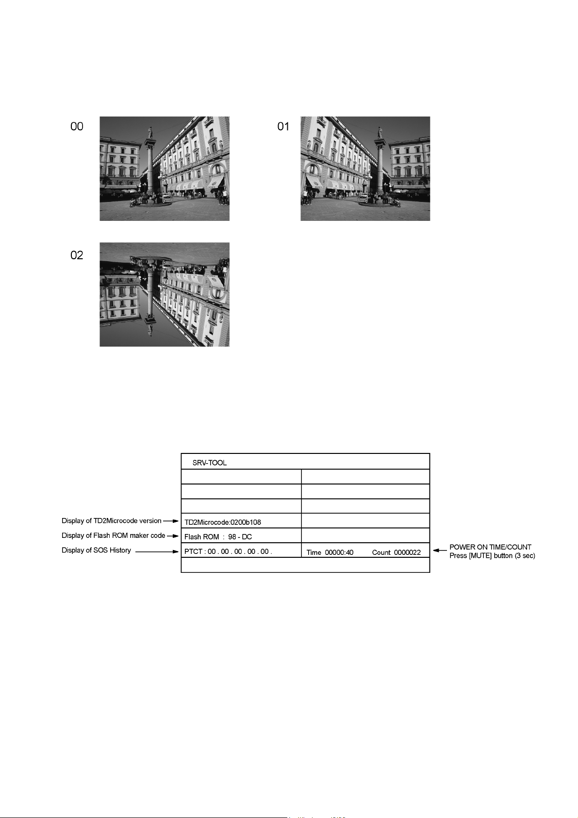
Picture can be reversed left and right or up and down.
00 : Default (Normal picture is displayed)
01 : Picture is reversed left and right.
02 : Picture is reversed up and down.
Hint : If the defective symptom (e.g. Vertical bar or Horizontal bar) is moved by selection of this mirror, the possible cause is in
A-board.
6.3. Service tool mode
6.3.1. How to access
1. Select [SRV-TOOL] in Service Mode.
2. Press [OK] button on the remote control.
6.3.2. Display of SOS History
SOS History (Number of LED blinking) indication.
From left side; Last SOS, before Last, three occurrence before, 2nd occurrence after shipment, 1st occurrence after shipment.
This indication will be cleared by [Self-check indication and forced to factory shipment setting].
6.3.3. POWER ON TIME/COUNT
Note : To display TIME/COUNT menu, highlight position, then press MUTE for 3 sec.
Time : Cumulative power on time, indicated hour : minute by decimal
Count : Number of ON times by decimal
Note : This indication will not be cleared by either of the self-checks or any other command.
6.3.4. Exit
1. Disconnect the AC cord from wall outlet or switch off the power with [ Power ] button on the main unit.
13
Page 14
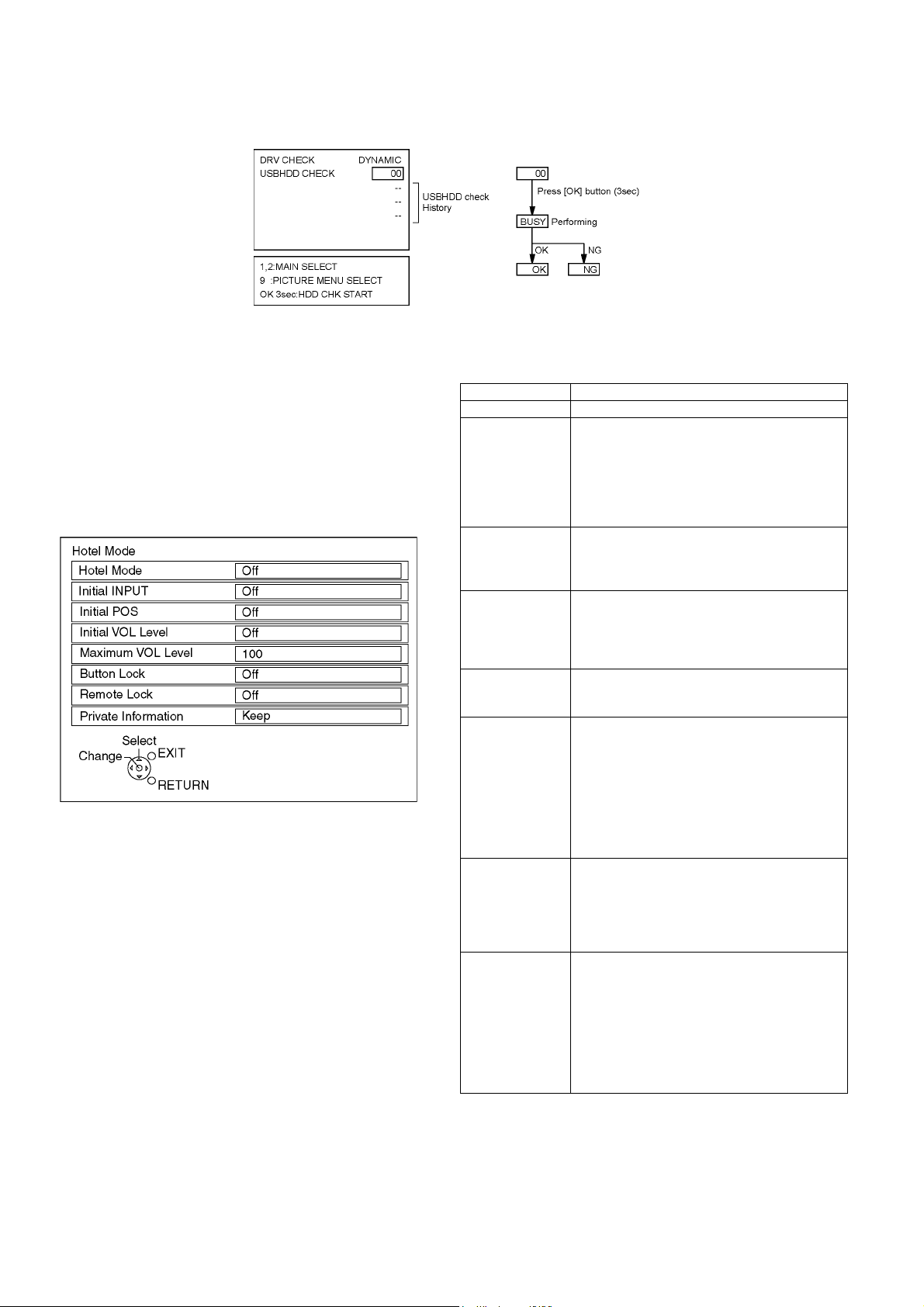
6.4. DRV Check - USB HDD Check
1. Select [DRV Check - USBHDD Check] in Service Mode.
2. Press [OK] button on the remote control for more than 3 seconds.
6.5. Hotel mode
1. Purpose
Restrict a function for hotels.
2. Access command to the Hotel mode setup menu
In order to display the Hotel mode setup menu:
While pressing [VOLUME (-)] button of the main unit,
press [AV] button of the remote control three times within
2 seconds.
Then, the Hotel mode setup menu is displayed.
3. To exit the Hotel mode setup menu
Disconnect AC power cord from wall outlet.
4. Explain the Hotel mode setup menu
Item Function
Hotel Mode Select hotel mode On/Off
Initial INPUT Select input signal modes.
Set the input, when each time power is switched
on.
Selection :
Off,Analogue TV,Digital TV,AV1,AV2,PC,HDMI1,
HDMI2,HDMI3
• Off: give priority to a last memory.
Initial POS Select programme number.
Initial VOL Level Adjust the volume when each time power is
Maximum VOL
Level
Button Lock Select local key conditions.
Remote Lock Select remote control key conditions.
Private Information Select private information for VIERA Cast is Keep
Selection :
Off/0 to 99
• Off: give priority to a last memory
switched on.
Selection/Range :
Off/0 to 100
• Off: give priority to a last memory
Adjust maximum volume.
Range :
0 to 100
Selection :
Off/SETUP/MENU/ALL
• Off: altogether valid
• SETUP: only F-key is invalid
(Tuning guide (menu) can not be selected.)
• MENU: only F-key is invalid
(only Volume/Mute can be selected.)
• ALL: altogether invalid.
Selection :
Off/SETUP/MENU
• Off: altogether valid
• SETUP: only Setup menu is invalid
• MENU: Picture/Sound/Setup menu are invalid
or Reset if Hotel mode is set to [On] when TV
power on.
Selection :
Keep/Reset
• Keep: private information for VIERA Cast is
keep
• Reset: private information for VIERA Cast is
reset
14
Page 15
6.6. Data Copy by SD Card
6.6.1. Purpose
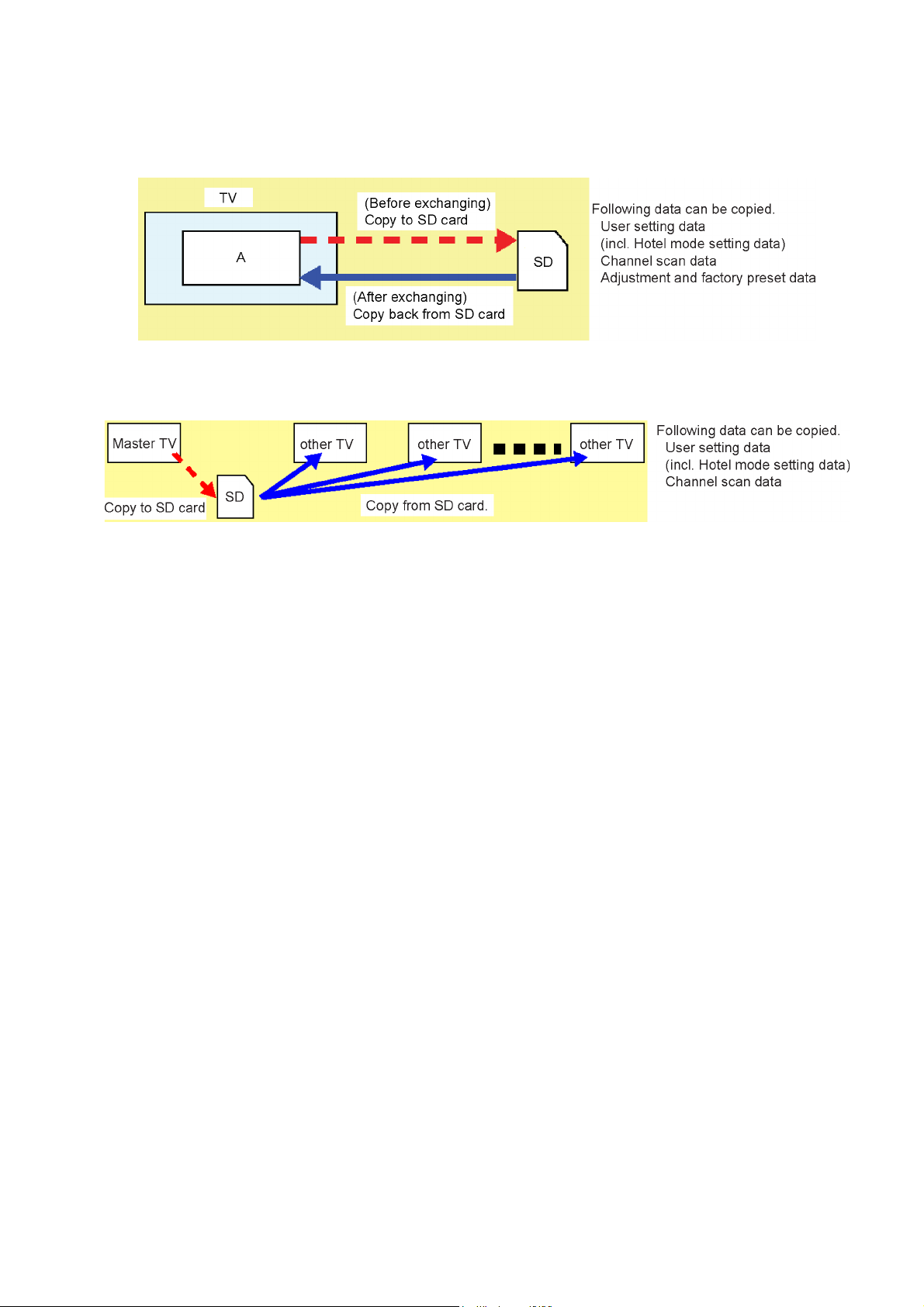
(a) Board replacement (Copy the data when exchanging A-board):
When exchanging A-board, the data in original A-board can be copied to SD card and then copy to new A-board.
(b) Hotel (Copy the data when installing a number of units in hotel or any facility):
When installing a number of units in hotel or any facility, the data in master TV can be copied to SD card and then copy to other
TVs.
6.6.2. Preparation
Make pwd file as startup file for (a) or (b) in a empty SD card.
1. Insert a empty SD card to your PC.
2. Right-click a blank area in a SD card window, point to New, and then click text document. A new file is created by default
(New Text Document.txt).
3. Right-click the new text document that you just created and select rename, and then change the name and extension of the
file to the following file name for (a) or (b) and press ENTER.
File name:
(a) For Board replacement : boardreplace.pwd
(b) For Hotel : hotel.pwd
Note:
Please make only one file to prevent the operation error.
No any other file should not be in SD card.
15
Page 16
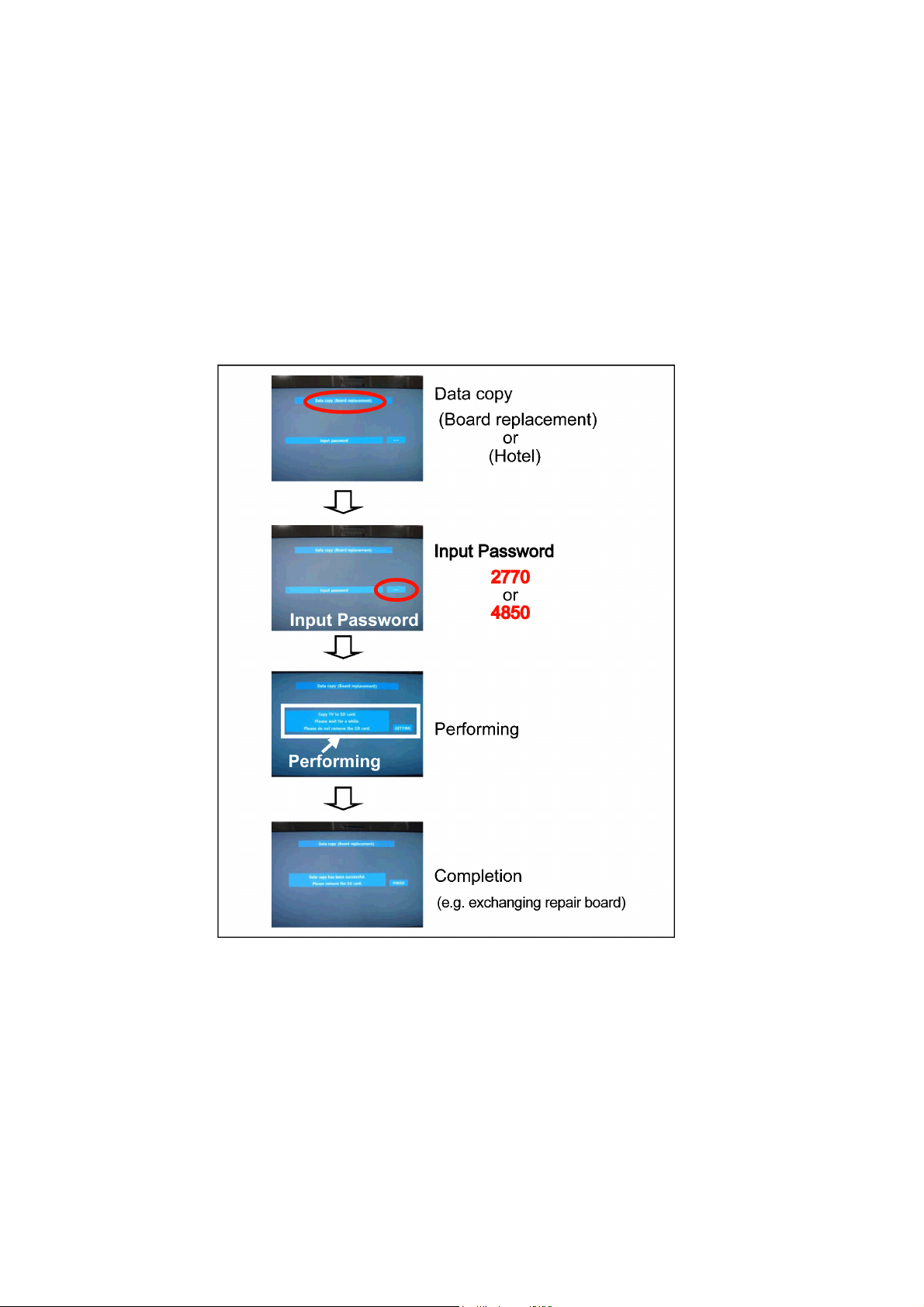
6.6.3. Data copy from TV set to SD Card
1. Turn on the TV set.
2. Insert SD card with a startup file (pwd file) to SD slot.
On-screen Display will be appeared according to the startup file automatically.
3. Input a following password for (a) or (b) by using remote control.
(a) For Board replacement : 2770
(b) For Hotel : 4850
Data will be copied from TV set to SD card.
It takes around 2 to 6 minutes maximum for copying.
4. After the completion of copying to SD card, remove SD card from TV set.
5. Turn off the TV set.
Note:
Following new folder will be created in SD card for data from TV set.
(a) For Board replacement : user_setup
(b) For Hotel : hotel
16
Page 17
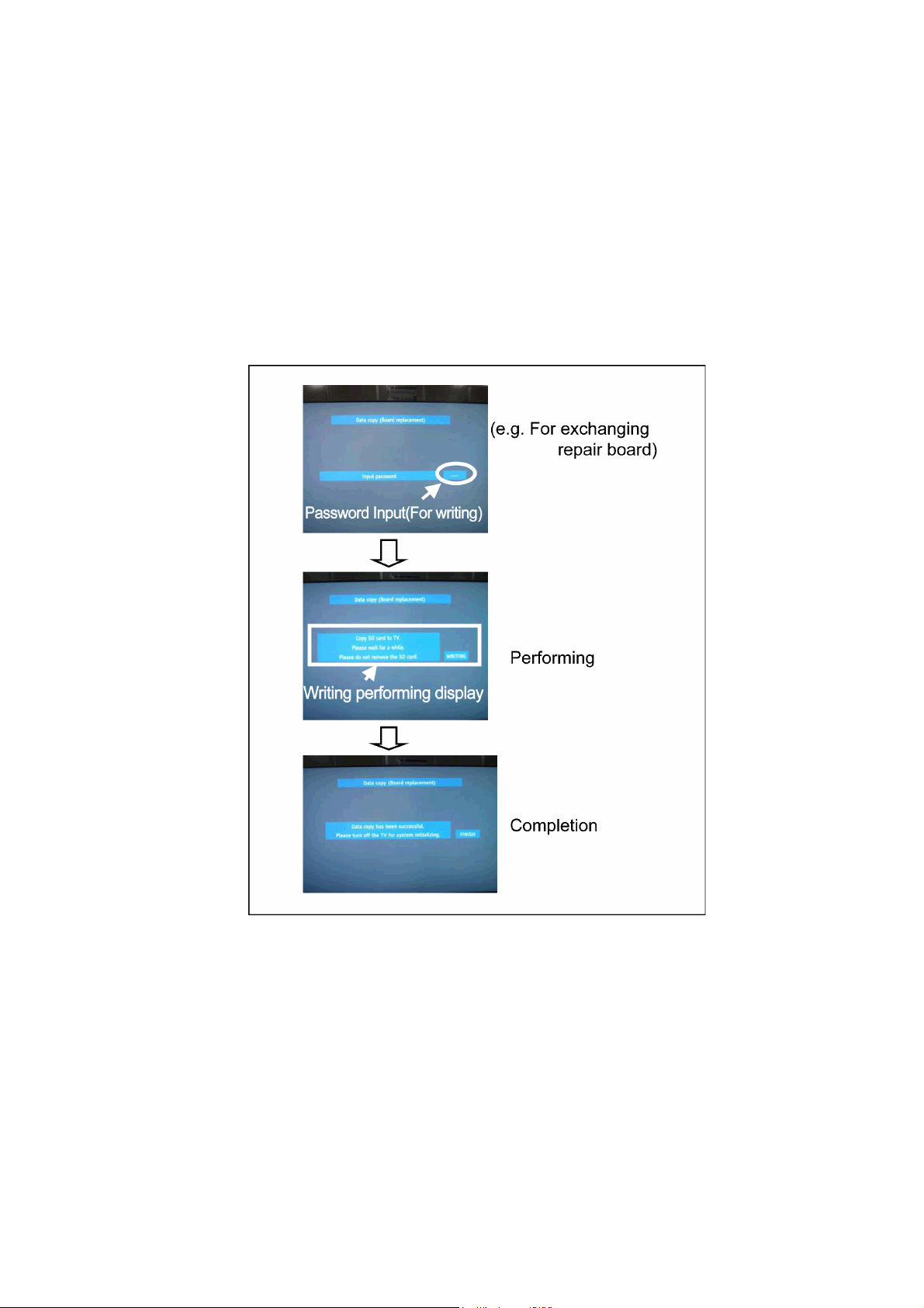
6.6.4. Data copy from SD Card to TV set
1. Turn on the TV set.
2. Insert SD card with Data to SD slot.
On-screen Display will be appeared according to the Data folder automatically.
3. Input a following password for (a) or (b) by using remote control.
(a) For Board replacement : 2771
(b) For Hotel : 4851
Data will be copied from SD card to TV set.
4. After the completion of copying to SD card, remove SD card from TV set.
(a) For Board replacement : Data will be deleted after copying (Limited one copy).
(b) For Hotel : Data will not be deleted and can be used for other TVs.
5. Turn off the TV set.
Note:
1. Depending on the failure of boards, function of Data copy for board replacement does not work.
2. This function can be effective among the same model numbers.
17
Page 18
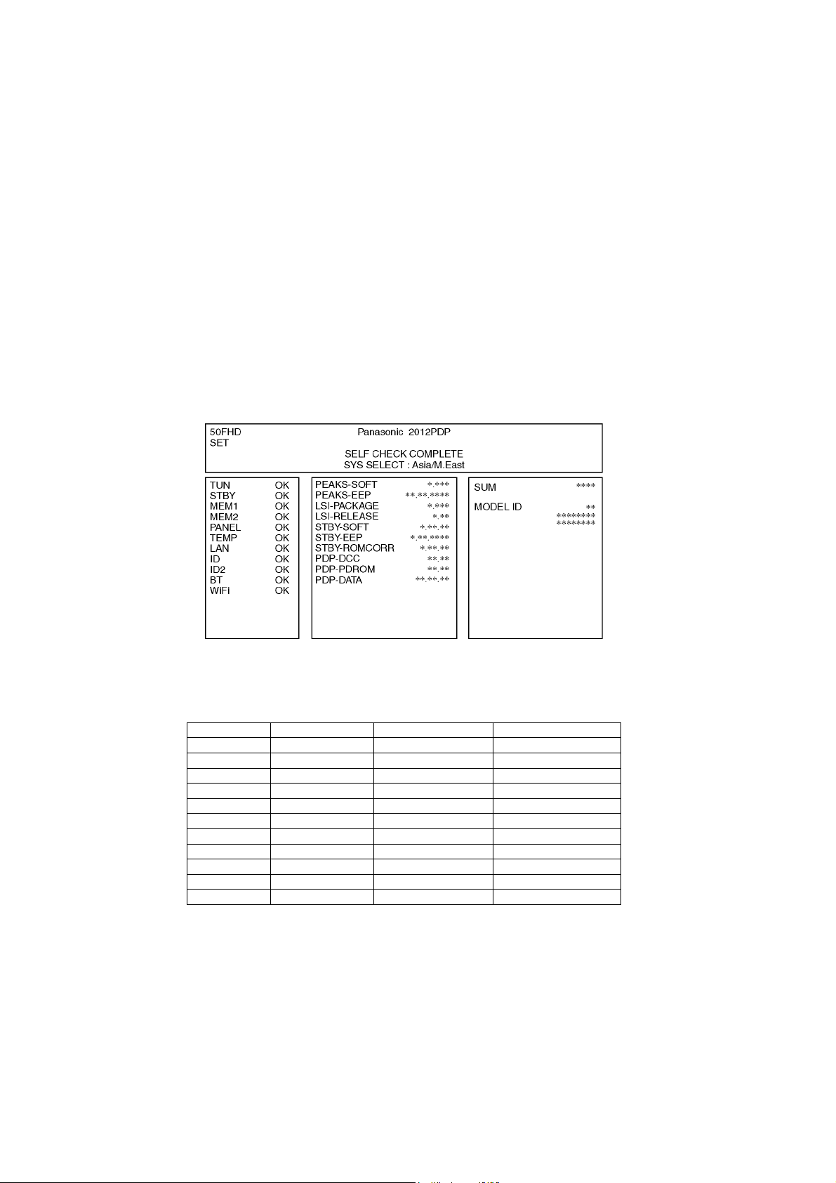
7 Troubleshooting Guide
Use the self-check function to test the unit.
1. Checking the IIC bus lines
2. Power LED Blinking timing
7.1. Check of the IIC bus lines
7.1.1. How to access
7.1.1.1. Self-check indication only:
Produce TV reception screen, and while pressing [VOLUME ( - )] button on the main unit, press [OK] button on the remote control
for more than 3 seconds.
7.1.1.2. Self-check indication and forced to factory shipment setting:
Caution:
New key will be generated and previous TV programmes recorded in USB HDD will not be viewed. (See USB HDD
Recording) (A/Z only)
Produce TV reception screen, and while pressing [VOLUME ( - )] button on the main unit, press [MENU] button on the remote
control for more than 3 seconds.
7.1.2. Screen display
7.1.3. Check Point
Confirm the following parts if NG was displayed.
DISPLAY Check Ref. No. Description Check Point
TUN TU6705 TUNER A-BOARD
STBY IC8000 PEAKS-LD4(STM) A-BOARD
MEM1 IC8902 PEAKS EEPROM A-BOARD
MEM2 IC8900 NAND FLASH A-BOARD
PANEL IC9300 PD6H A-BOARD
TEMP IC2001 TEMP SENSOR A-BOARD
LAN IC8650 ETHERPHY A-BOARD
ID ID A-BOARD
ID2 ID2 A-BOARD
BT IC8000, A50 BLUETOOTH A-BOARD/BLUETOOTH
WiFi IC8000, JK8605 WiFi A-BOARD/WiFi
7.1.4. Exit
Disconnect the AC cord from wall outlet or switch off the power with [ Power ] button on the main unit.
18
Page 19
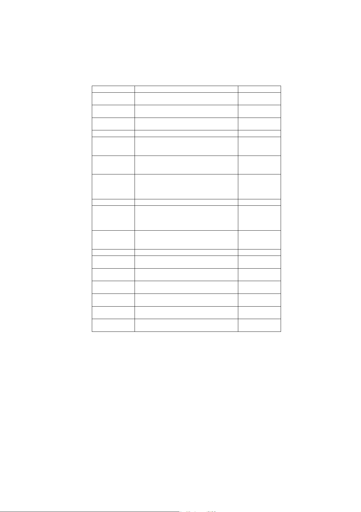
7.2. Power LED Blinking timing chart
1. Subject
Information of LED Flashing timing chart.
2. Contents
When an abnormality has occurred the unit, the protection circuit operates and reset to the stand by mode. At this time, the
defective block can be identified by the number of blinks of the Power LED on the front panel of the unit.
Blinking Times Contents Check point
1 Panel information SOS
PD Start SOS
2 P+15V SOS A-Board
3 IROM BOOT PROGRAM SOS A-Board
4 Power SOS P-Board
6 Driver SOS1
(SC Energy recovery circuit)
(A-SC FPC DET)
7 Driver SOS2
(SU/SD Connector DET)
(SU/SD Scan and Logic IC)
8 Driver SOS3
(SS FPC DET)
(SS Energy recovery circuit)
9 Discharge Control SOS A-Board
10 Sub 3.3V SOS
Tuner power SOS
BE SOS
12 Sound SOS A-Board
13 Emergency SOS A-Board
20 2nd BOOT PROGRAM SOS
(Watchdog timer over flow)
21 2nd BOOT PROGRAM SOS
(System error)
22 2nd BOOT PROGRAM SOS
(Main system bus freeze)
23 2nd BOOT PROGRAM SOS
(Accidental interrupt signal)
24 2nd BOOT PROGRAM SOS
(NAND Flash memory data transfer error finish)
25 2nd BOOT PROGRAM SOS
(Unsupported NAND Flash memory)
-
P-Board
P-Board
SC-Board
A-SC FPC
SU-Board
SD-Board
*
SS-Board
SS2-Board
SS FPC
SS2 FPC
A-Board
SC-Board
SS-Board
P-Board
Speaker
Woofer
A-Board
A-Board
A-Board
A-Board
A-Board
A-Board
*Use SC jig to isolate the board.
19
Page 20
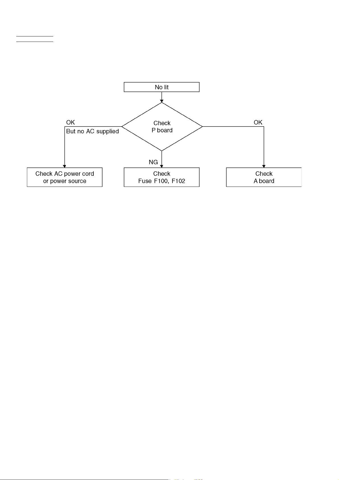
7.3. No Power
First check point
There are following 3 states of No Power indication by power LED.
1. No lit
2. Green is lit then turns red blinking a few seconds later. (See Power LED Blinking timing chart)
3. Only red is lit.
20
Page 21
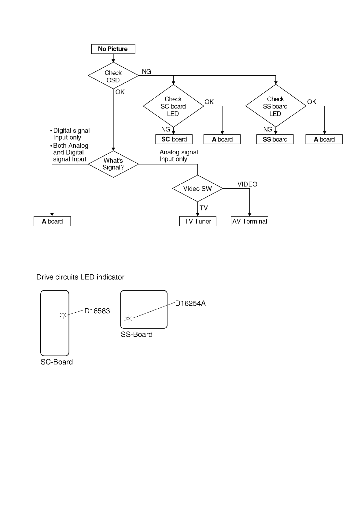
7.4. No Picture
21
Page 22
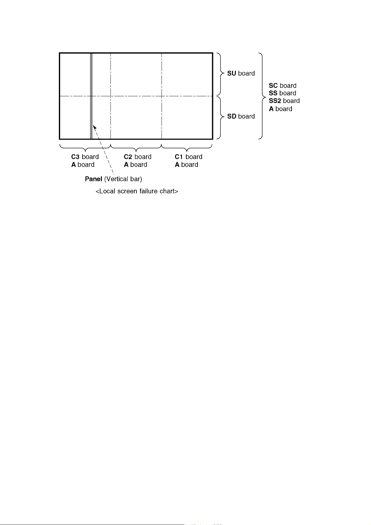
7.5. Local screen failure
Plasma display may have local area failure on the screen. Fig-1 is the possible defect P.C.B. for each local area.
Fig-1
22
Page 23
8 Service Fixture & Tools
8.1. SC jig
Purpose:
To find the failure board (SC or SU/SD) when the power LED is blinking 7 times.
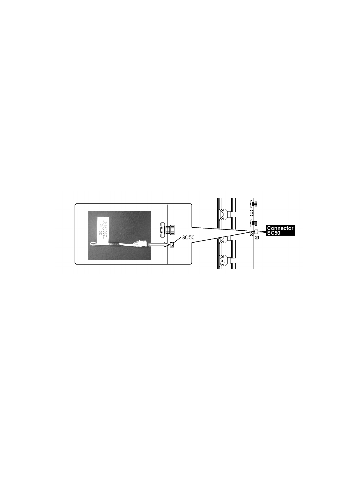
SC jig:
Jumper connector to connect to SC50 connector on SC board
Part number:
TZSC09187
How to use:
Caution: Remove SC jig from SC board after inspection.
1. Remove all connector between SC board and SU/SD board to isolate SC board from both SU and SD board electrically.
Note: The board will be damaged if all connector is not removed (for example; remove connector only for SU board and stay
connecting with SD board. The board will be damaged.)
2. Connect SC jig to connector SC50 at left bottom side of SC board
3. Turn on the TV/Display Unit and confirm the power LED blinking.
LED blinking: Possible cause of failure is in SC board
No LED blinking (Lighting or no lighting): Possible cause of failure is in SU or SD board
4. After inspection, turn off the TV/Display Unit and wait a few minutes to discharge.
5. Remove SC jig from SC board.
Remark: This SC jig can be used for all 2012 Plasma TV and Plasma Display.
23
Page 24
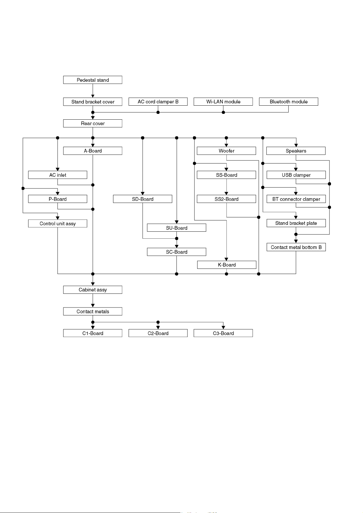
9 Disassembly and Assembly Instructions
9.1. Disassembly Flow Chart for the Unit
This is a disassembly chart.
When assembling, perform this chart conversely.
24
Page 25
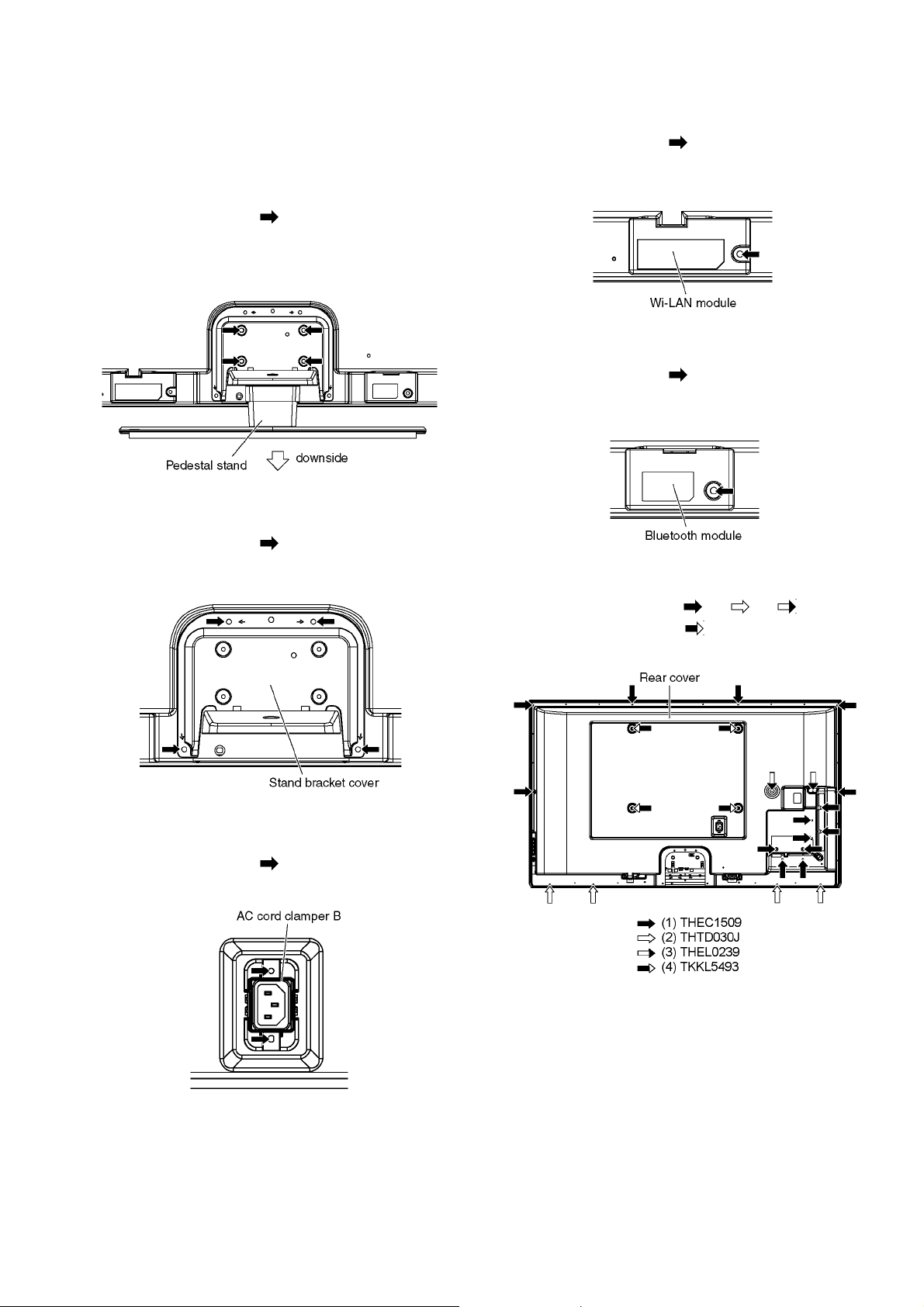
9.2. Disassembly Procedure for the Unit
9.2.1. Remove the Pedestal stand
1. Remove the Plasma panel section from the servicing
stand and lay on a flat surface such as a table (covered
by a soft cloth) with the Plasma panel surface facing
downward.
2. Remove the screws (×4 )
3. Slide the Pedestal stand to the downside and remove the
Pedestal stand.
9.2.2. Remove the Stand bracket cover
1. Remove the screws (×4 ) and remove the Stand
bracket cover.
9.2.4. Remove the Wi-LAN module
1. Remove the screw (×1 ) and remove the Wi-LAN
module.
9.2.5. Remove the Bluetooth module
1. Remove the screw (×1 ) and remove the Bluetooth
module.
9.2.6. Remove the Rear cover
1. Remove the screws (×14 , ×4 , ×2 ).
2. Remove the M8 caps (×4 ).
3. Remove the Rear cover.
9.2.3. Remove the AC cord clamper B
1. Remove the screws (×2 ) and remove the AC cord
clamper B.
25
Page 26
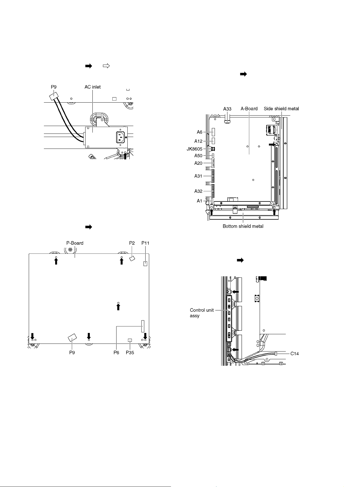
9.2.7. Remove the AC inlet
Caution:
To remove AC inlet wait 1 minute after power was off for
discharge from electrolysis capacitors.
1. Disconnect the connector (P9).
2. Remove the screws (×1 , ×1 ) and remove the AC
inlet.
9.2.8. Remove the P-Board
Caution:
To remove P.C.B. wait 1 minute after power was off for
discharge from electrolysis capacitors.
1. Unlock the cable clampers and the tapes to free the
cables
2. Disconnect the connectors (P2, P6, P9, P11 and P35).
3. Remove the screws (×6 ) and remove the P-Board.
9.2.9. Remove the A-Board
1. Unlock the cable clampers and the tapes to free the
cables.
2. Disconnect the connectors (A1, A6, A12 and A50).
3. Disconnect the USB cable (JK8605).
4. Disconnect the flexible cables (A20, A31, A32 and A33).
5. Remove the screws (×3 ).
6. Remove the Side shield metal and the Bottom shield
metal.
7. Remove the A-Board.
9.2.10. Remove the Control unit assy
1. Disconnect the connector (C14).
2. Remove the claws (×2 ) and remove the Control unit
assy.
26
Page 27
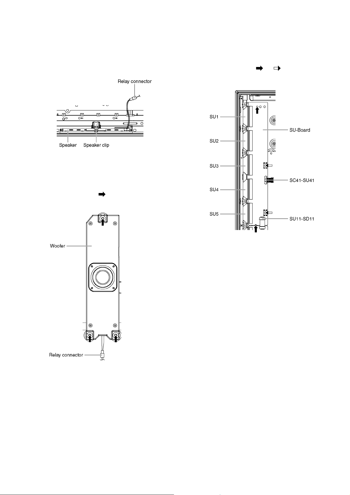
9.2.11. Remove the Speakers
1. Unlock the cable clampers and the tapes to free the
cables.
2. Disconnect the Relay connector.
3. Remove the Speaker clip (each) and remove the
Speakers (L, R).
9.2.12. Remove the Woofer
1. Unlock the cable clampers and the tapes to free the
cables.
2. Disconnect the Relay connector.
3. Remove the screws (×3 ).
4. Remove the Woofer.
9.2.13. Remove the SU-Board
1. Disconnect the flexible cables (SU1, SU2, SU3, SU4 and
SU5) connected to the SU-Board.
2. Disconnect the flexible cable (SU11-SD11) and the bridge
connector (SC41-SU41).
3. Remove the screws (×2 , ×2 ) and remove the SU-
Board.
27
Page 28
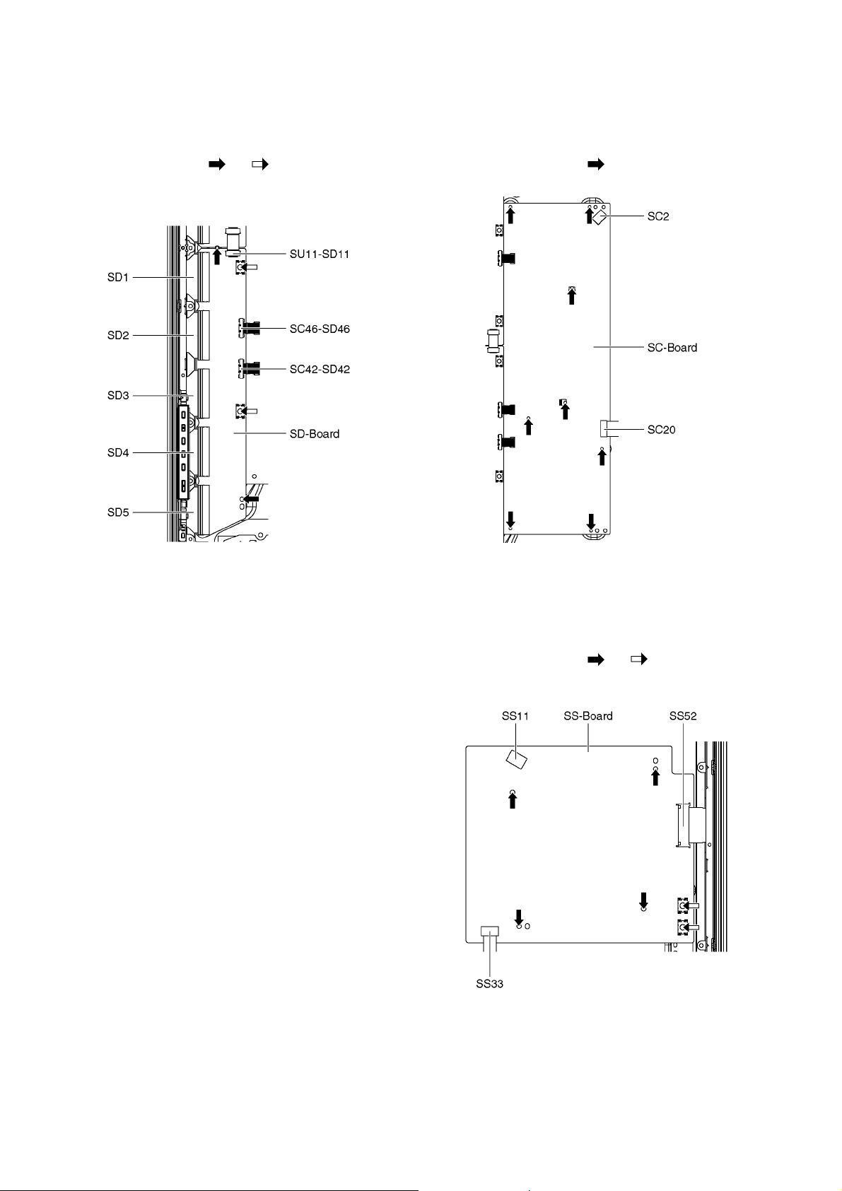
9.2.14. Remove the SD-Board
1. Disconnect the flexible cables (SD1, SD2, SD3, SD4 and
SD5) connected to the SD-Board.
2. Disconnect the flexible cable (SU11-SD11) and the bridge
connectors (SC42-SD42 and SC46-SD46).
3. Remove the screws (×2 , ×2 ) and remove the SD-
Board.
9.2.15. Remove the SC-Board
1. Unlock the cable clampers and the tapes to free the
cables.
2. Disconnect the connector (SC2).
3. Disconnect the flexible cable (SC20).
4. Remove the screws (×8 ) and remove the SC-Board.
9.2.16. Remove the SS-Board
1. Disconnect the connector (SS11).
2. Disconnect the flexible cable (SS33).
3. Disconnect the flexible cable (SS52).
4. Remove the screws (×4 , ×2 ) and remove the SS-
Board.
28
Page 29
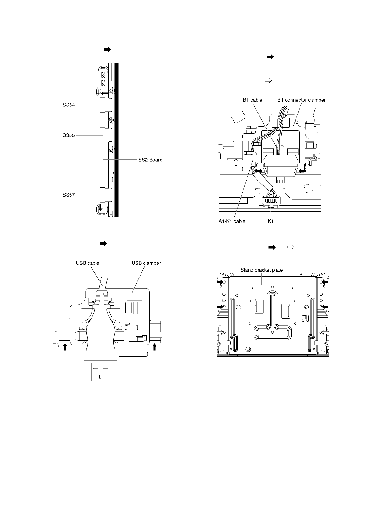
9.2.17. Remove the SS2-Board
1. Disconnect the flexible cables (SS54, SS55 and SS57).
2. Remove the screws (×2 ) and remove the SS2-Board.
9.2.19. Remove the BT connector clamper
1. Unlock the cable clampers and the tapes to free the
cables.
2. Remove the claws (×2 ) and remove the BT cable.
3. Disconnect the connector (K1) and remove the A1-K1
cable.
4. Remove the claws (×2 ) and remove the BT connector
clamper.
9.2.18. Remove the USB clamper
1. Remove the claws (×2 ) and remove the USB clamper.
2. Remove the USB cable from the USB clamper.
9.2.20. Remove the Stand bracket plate
1. Remove the screws (×4 , ×2 ) and remove the
Stand bracket plate.
29
Page 30
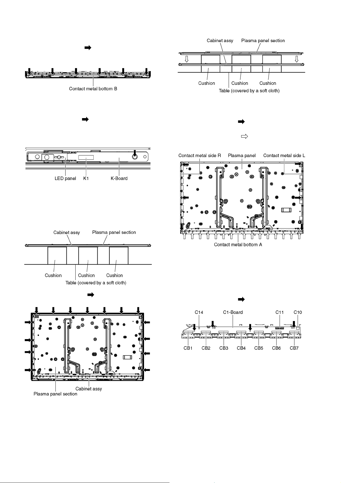
9.2.21. Remove the Contact metal bottom B
1. Remove the screws (×6 ).
2. Remove the Contact metal bottom B.
3. Remove the Cabinet assy from the Plasma panel section.
9.2.22. Remove the K-Board
1. Remove the screw (×1 ).
2. Disconnect the connector (K1) and remove the K-Board
from the LED panel.
9.2.23. Remove the Cabinet assy from the Plasma panel section.
1. Place the Cabinet assy on a flat surface of a table
(covered by a soft cloth) and a cushion.
2. Remove the screws (×15 ).
9.2.24. Remove the Contact metals
1. Remove the Tape from the Contact metals.
2. Remove the screws (×6 ).
3. Remove the Contact metal side (L, R).
4. Remove the screws (×15 ).
5. Remove the Contact metal bottom A.
9.2.25. Remove the C1-Board
1. Disconnect the flexible cables (CB1, CB2, CB3, CB4,
CB5, CB6 and CB7).
2. Disconnect the flexible cable (C11).
3. Disconnect the connectors (C10 and C14).
4. Remove the screws (×4 ) and remove the C1-Board.
30
Page 31
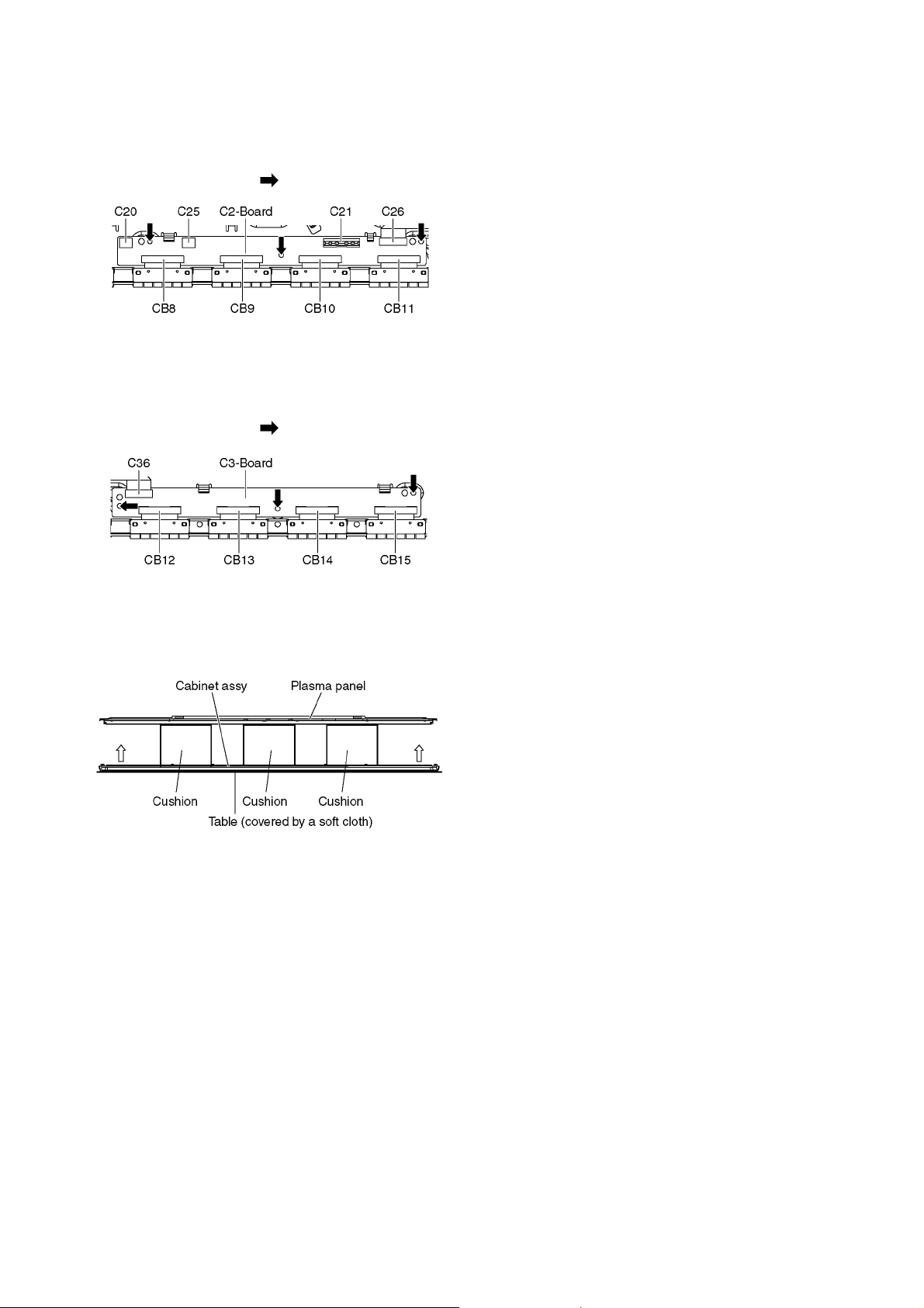
9.2.26. Remove the C2-Board
1. Disconnect the flexible cables (CB8, CB9, CB10 and
CB11).
2. Disconnect the flexible cables (C21 and C26).
3. Disconnect the connectors (C20 and C25).
4. Remove the screws (×3 ) and remove the C2-Board.
9.2.27. Remove the C3-Board
1. Disconnect the flexible cables (CB12, CB13, CB14 and
CB15).
2. Disconnect the flexible cable (C36).
3. Remove the screws (×3 ) and remove the C3-Board.
9.2.28. Replace the Plasma panel
Caution:
Place the Plasma panel on a flat surface of a table
(covered by a soft cloth) and a cushion.
A new Plasma panel itself without Contact metals is fragile.
To avoid the damage to new Plasma panel, carry a new
Plasma panel taking hold of the Contact metals.
1. Place a carton box packed a new Plasma panel on the
flat surface of the work bench.
2. Open a box and without taking a new Plasma panel.
3. Attach the Cabinet assy and each P.C.Board and so on,
to the new Plasma panel.
31
Page 32
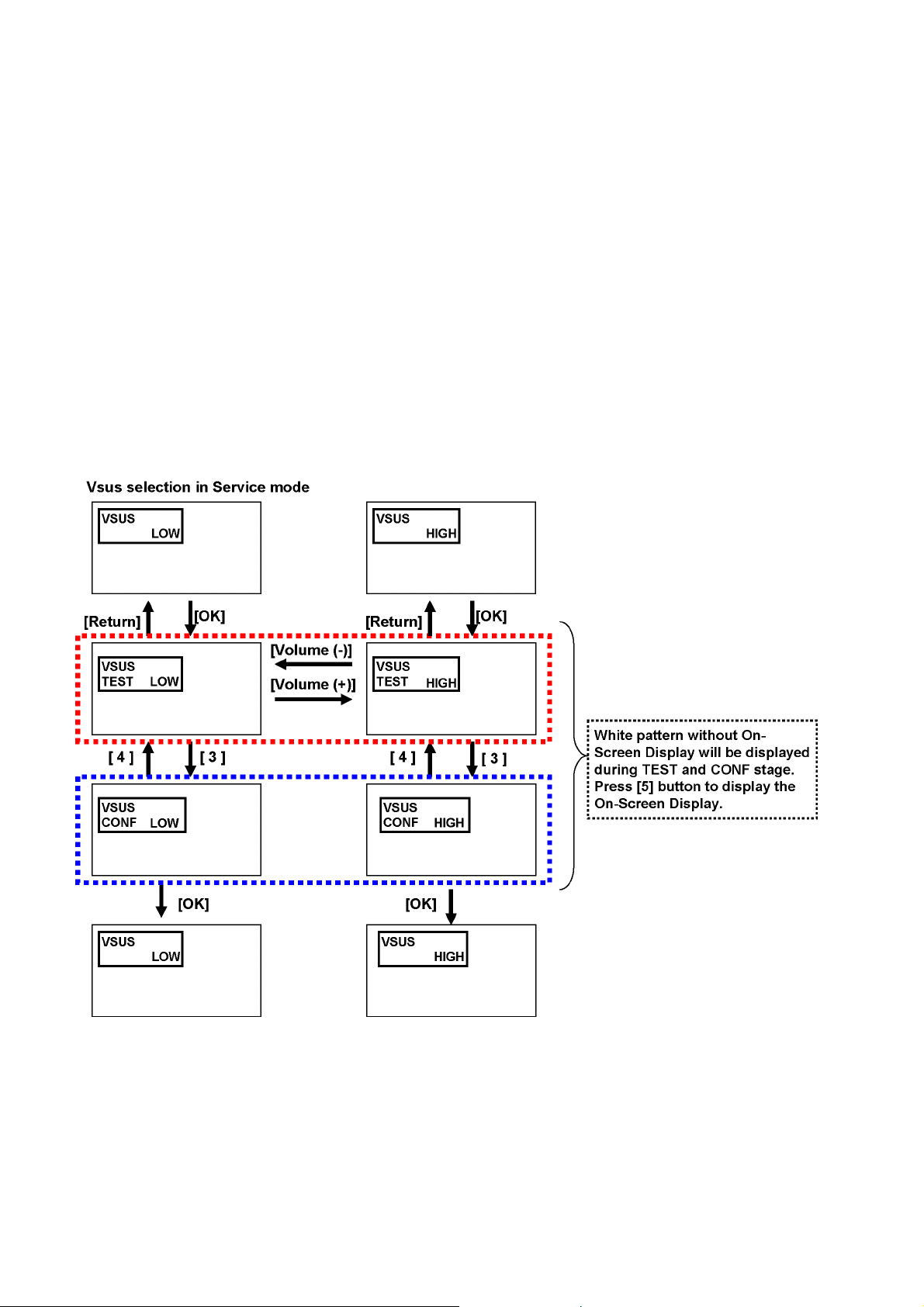
10 Measurements and Adjustments
10.1. Adjustment
10.1.1. Vsus selection
Caution:
When Plasma panel or A-board is replaced, Vsus should be set to LOW or HIGH.
Procedure
1. Go into main item [VSUS] in Service Mode. LOW or HIGH will be displayed.
2. Press [OK] button to go to TEST stage.
White pattern without On-Screen Display will be displayed during TEST and CONF stage. Press [5] button to display the
On-Screen Display.
3. Press [VOL (-)] button to set to LOW.
4. In LOW setting
a. If no several dead pixel is visible remarkably in white pattern, press [3] button to go to CONF stage.
b. If the several dead pixels are visible remarkably in white pattern, Set to HIGH by press [VOL (+)] button. Press [3] button
to go to CONF stage if the symptom is improved.
5. Press [OK] button in CONF stage to store LOW or HIGH.
6. Exit Service Mode by pressing [Power] button.
Notes:
Do not overwrite because data is written in Peaks-EEPROM after executing adjustment of V-SUS Voltage.
32
Page 33
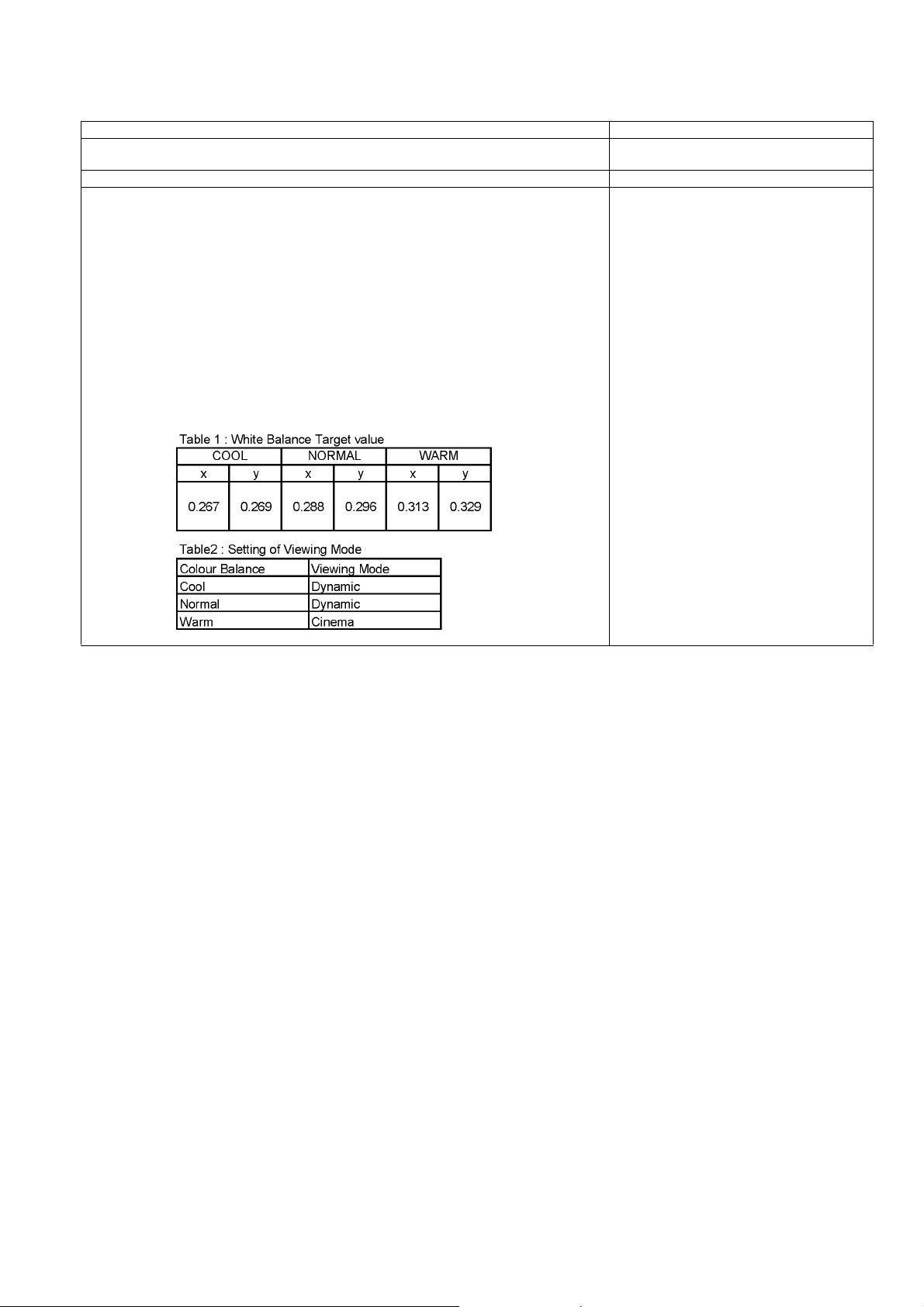
10.1.2. White balance adjustment
Name of measuring instrument Remarks
Color analyzer
(Minolta CS-2000 or equivalent)
Procedure Remarks
1. Enter the Service mode.
2. Receive the Analog-RF (except for no signal) or set CVBS/YUV/HDMI (no signal is
available).
3. Select [WB-ADJ] by using [1] and [2] key in the remote controller.
4. Check that the colour balance and the viewing mode is the values written in table1 and 2.
5. [INNER PATTERN] is displayed by using [5] key by using [5] key in the remote controller.
6. Select [G-CUTOFF] by using the [3] and [4] key in the remote controller, and set the value
to [80] by using the volume [+] and [-] key.
Also, [B-CUTOFF] and [R-CUTOFF] set to [80]
7. Set [G-DRIVE] value to the initial data (ex. D0).
8. Set the color analyzer and adjust color point to the values written in table1 by using [BDRIVE] and [R-DRIVE]
9. Increase RGB-DRIVE value so that the maximum drive value of one of R-DRIVE or GDRIVE or B-DRIVE should become [FF]
([ALL-DRIVE] set to [FF].)
33
Page 34

34
Page 35
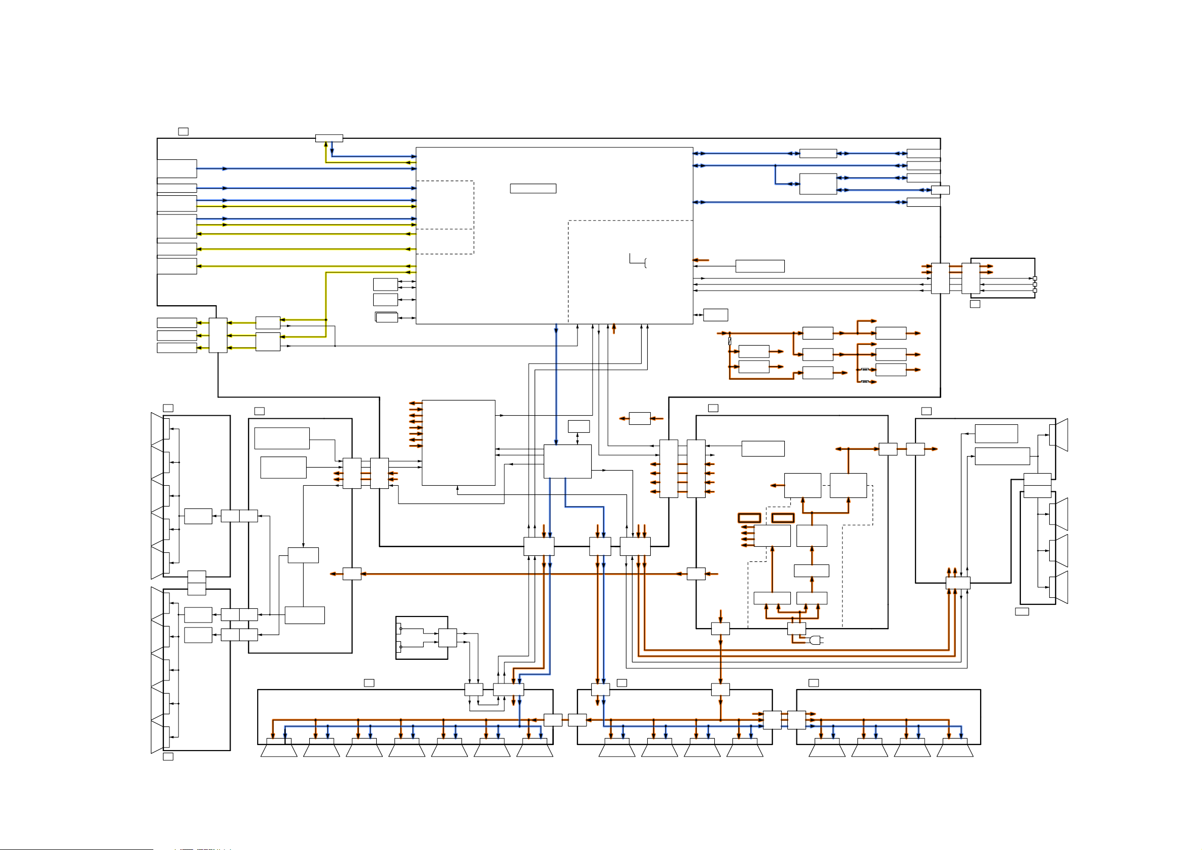
11 Block Diagram
11.1. Main Block Diagram
MAIN AV INPUT,PROCESSING
A
TUNER
AV2 VIDEO/
COMPONENT
AV1
AUDIO OUT
HEADPHONE
DIGITAL
AUDIO OUT
WOOFER
SPEAKER(L)
SPEAKER(R)
IFD_OUT
R/G/B/H/V
PC
V/Y/PB/PR
L/R
V
L/R
L/R OUT
HP L/R
DIGITAL AUDIO OUT
WO
L
A12
R
AUDIO
AMP2
AUDIO
AMP
ARC
(HDMI2)
HDMI1-3
TMDS DATA
NAND
FLASH
PEAKS
EEPROM
DDR3
HDMI I/F
ARC_OUT
TUNER I/F
R/G/B/H/V
V/YPbPr/RGB/YC
L/R
CVBS
L/R
LO1_L/R
HP_L/R
IEC_OUT
ASDOUT0
NAND FLASH I/F
CPU BUS
IIC1
DDR3 I/F
AV IN
AUDIO
OUT
PEAKS-LD4
LVDS I/F
STM
(LED:12TIMES)
SOUND_SOS
PANEL_SOS
(LED:10TIMES)
(LED:2TIMES)
(LED:4TIMES)
SOS4_PS
P+15V_DET
PANEL_MAIN_ON
P+15V
LAN CON I/F
SD CARD I/F
SUB+3.3V_SENSE
TUNER_POWER_SOS
REMOTE_IN
C.A.T.S_SENSOR
DMD IIC1
KEY1
KEY3
USB I/F
LED_R/G
SUB3.3V
TEMP
SENSOR
F15V
TUNER_POWER_SOS
(LED:10TIMES)
DCDC
SUB1.5V
DCDC
SUB1.1V
DCDC15V
USB
SUB1.5V
SUB1.1V
ETHERPHY
USB HUB
DCDC
SUB5V
DCDC
SUB3.3V
DCDC
P+1.2V
SUB5V
SUB3.3V
P+1.2V
ETHERNET DATA
SD CARD DATA
SUB5V
SUB3.3V
P
P+3.3V
P
USB
DP/DM
DCDC
P+5V
DCDC
SUB1.8V
DCDC
P+2.5V
DP/DM
SUB3.3V
STB3.3V
ETHERNET
USB_1-2
WiFi
SD CARD
P+5V
SUB1.8V
P+2.5V
A50
A1
BLUETOOTH
K1
SUB3.3V
STB3.3V
POWER LED
K
REMOTE RECEIVER
C.A.T.S. SENSOR
LED_R/G
REMOTE_RECEIVER
C.A.T.S_SENSOR
SU
SCAN OUT (UPPER)
SCAN
DRIVER
SU11
SD11
SCAN
DRIVER
LOGIC
SU41
SD42
SD46
SC
SC-BOARD
ENERGY RECOVERY
SOS DETECT
SC41
SC42
SC46
SCAN DRIVE
(LED:6TIMES)
SC-BOARD
FLOATING PART
SOS DETECT
(LED:7TIMES)
CONTROL
PULSE
VSCAN GEN.
VAD GEN.
SOS6_SC1
SOS7_SC2
P+5V
P+15V
SCAN CONTROL
VSUS
SC20
SC2
VDDSD
18V33V
STB3.3V
P+3.3V
SOS6_SC1
SOS7_SC2
A20
OPERATION
KEYS
POWER SW
DATA DRIVER (RIGHT)
C1
STB5V
F15V
SUB5V
SUB9V
SOS6_SC1
SOS7_SC2
P+5V
P+15V
SCAN CONTROL
CONTROL UNIT ASSY
ANALOG-ASIC
(LED:9TIMES)
(LED:6TIMES)
(LED:7TIMES)
SOS8_SS
(LED:8TIMES)
PANEL_SOSSTB1.1V
FFC_OFF_DET
SOS_DCC
KEYSCAN
KEY3
C14
KEY1
KEY3
A31
VIDEO DATA
P+3.3V
LVDS DATA
PD6H
SPI
FLASH
VIDEO DATA
SUSTAIN
CONTROL
SOS8_SS
P+3.3V
A32
STB5V
DCDC
STB5V
SOS4_PS
PANEL_MAIN_ON
SOUND15V
A33
EV5V
P+15V
F15V
P+5V
EV5V
A6
P+15V
P6
P2
POWER SUPPLY
POWER SUPPLY
P
P
SOS4_PS
PANEL_
MAIN_ON
SOUND15V
EV5V
P+15V
F15V
STB5V
P+15V
F15V
SOUND15V
VSUS
P-BOARD
SOS DETECT
(LED:4TIMES)
VDA
STANDBY
VOLTAGE
CONVERTER
HOTCOLD
PROCESS
VOLTAGE
CONVERTER
POWER
FACTOR
CONTROL
RECTIFIER
VSUS
SUSTAIN
VOLTAGE
CONVERTER
VSUS
SUSTAIN DRIVE
SS
SS-BOARD
SOS DETECT
SOS8_SS
SUSTAIN CONTROL
P+5V
(LED:8TIMES)
VSUS GEN.
VE GEN.
ENERGY RECOVERY
ZA16101
ZA16106
ZA16111
ZA16116
SS11
VSUS
P+15V
P11
SS33
RECTIFIER
VDA
VIDEO DATA
KEYSCAN
KEY3
P+3.3V
C11
P+3.3V
VIDEO DATA
C21
P+15V
P+5V
SUSTAIN CONTROL
SOS8_SS
DATA DRIVER (CENTER)
C2
P35
C25
RELAY
P9
AC CORD
DATA DRIVER (LEFT)
C3
SS2
SUSTAIN
OUT
(LOWER)
SCAN OUT (LOWER)
SD
DATA
DRIVER
DATA
DRIVER
DATA
DRIVER
DATA
DRIVER
VDA
VIDEO DATA
DATA
DRIVER
DATA
DRIVER
P+3.3V
DATA
DRIVER
P+3.3V
C20
C10
DATA
DRIVER
DATA
DRIVER
VDA
VIDEO DATA
DATA
DRIVER
P+3.3V
DATA
DRIVER
C26
P+3.3V
C36
DATA
DRIVER
DATA
DRIVER
VDA
VIDEO DATA
DATA
DRIVER
DATA
DRIVER
35
Page 36
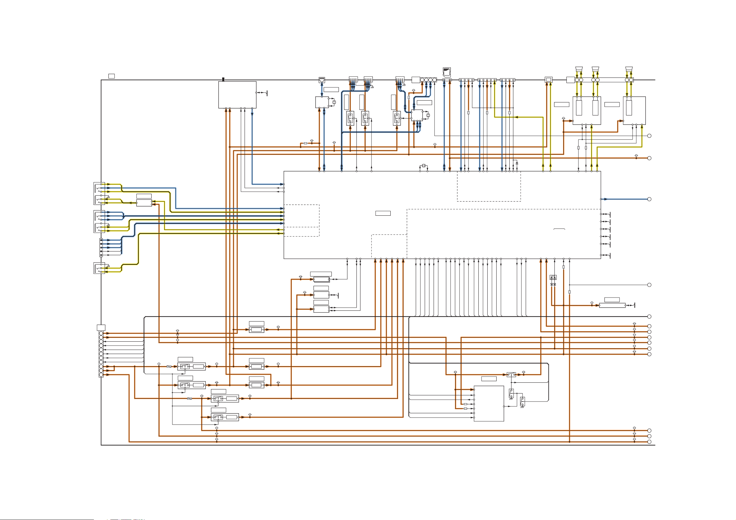
11.2. Block (1/4) Diagram
JK3101
AUDIO
OUT
JK3100
AV2 VIDEO/
COMPONENT
JK3202
HEADPHONE
PANEL_MAIN_ON
STB5V_SW_ON
TUNER_SUB_ON
AV1
JK3001
PC
SOUND15V
SOS4_PS
P+15V
EV5V
P_S1
P_S0
F15V
F15V
MAIN AV INPUT,PROCESSING
A
R
V
L
D1_R
D1_L
IC3051
L/RL_OUT
AUDIO
AMP
R_OUT
D1_PR
D1_PB
D1_Y/V
PC_R
PC_G
PC_B
PC_H
PC_V
HP_R
HP_L
ANT IN
Si_1.8V
TU6705
TUNER
Si_3.3V
FE_T_XRST
IFAGC1
IF1_P/N
DMD_
IIC0
IF1_P/N
FE_T_XRST
IFAGC1
CVBS
L/R
V/YPbPr/RGB/YC
L/R
R/G/B/H/V
LO1_L/R
HP_L/R
SUB1.5V
WOL3.3V
AV IN
AUDIO
OUT
JK8602A
ETHERNET
WOL3.3V
IC8200,01
IC8650
ETHERPHY
X8651
25MHz
SUB5V
LAN CON I/F
USB I/F
JK8603
USB1
IC8606
DDR3 I/F
JK8601
USB2
IC8602
USB1VBUS
NAND FLASH I/F
CPU BUS
USB2VBUS
IC8000
PEAKS-LD4
AVDDHP3.3V
VCC
HDMI3.3V
SUB3.3V
JK8605
WiFi
IC8603
SUB1.8V
SUB1.5V
SUB1.1V
A50
BT3.3V
BLUETOOTH
VBUS1
1 453
IC8601
USB HUB
X8600
12MHz
X8300
24.576MHz
AXO
REC_READY
STB_OFF
DP1
RF_LR
DM1
5
2
SUB3.3V
AXI
TUNER_SUB_ON
PANEL_MAIN_ON
CI_POWER_ON
JK8600
SD CARD
SD DATA:4bit
SD CARD I/F
SOS4_PS
(LED:4TIMES)
VDDSD1.8V3.3V
KEY1
KEY3
JK4702B
HDMI1
TMDS DATA
CLOCK
RX2
STM
XRSTSTM
DRVRST
+5V
DDC_IIC2
HDMI_CEC
DDC_IIC2
HDMI_5V_DET2
PD6H_XRST_SYS
XRST
JK4701B
HDMI2
DDC_IIC1
TMDS DATA
CLOCK
RX1
DDC_IIC1
HDMI I/F
R_LED_ON
REMOTE_IN
C.A.T.S_SENSOR
+5V
ARC
HDMI_CEC
HDMI_5V_DET1
PANEL_SOS
G_LED_ON
JK4700B
HDMI3
DDC_IIC0
TMDS DATA
CLOCK
RX0
POWER_DET
SW_OFF_DET
+5V
HDMI_CEC
HDMI_CEC
DDC_IIC0
HDMI_5V_DET0
HDMI_CEC_
PULL_ON
LOGO_ON
DISPEN
INIT_DONE
D3201
DIGITAL
AUDIO
ARC_OUT
STB1.1V
OUT
(LED:10TIMES)
STB3.3V
IC4900
AUDIO AMP
SOUND15V
IEC_OUT
TUNER_POWER_SOS
SUB3.3V_SENSE
D8771
SPEAKER_L
A12
P+15V_DET
1
2
L(+)
L(-)
L_OUT
SPEAKER
15V
SOUND_SOS
(LED:12TIMES)
(LED:2TIMES)
SOS
LVDS I/F
SPEAKER_R
R(-)
RESET
ASDOUT0
AMP_XRST
IIC0
IIC1
DMD_
IIC0
DMD_
IIC1
SBI0
SBO0
STM
IIC
3
R(+)
R_OUT
SPEAKER
ASDOUT1
IC4901
AUDIO AMP2
IIC0
IIC1
DMD_
IIC0
DMD_
IIC1
SBI0
SBO0
STM
IIC
WOOFER
6
WO(-)
WO(+)
WOOFER
15V
VDDSD18V33V
LVDS DATA
OUT
RESET
SOS
1
2
3
DDR3
DMD_
IIC1
4
5
6
7
8
9
10
11
12
13
14
IC8902
SUB3.3V
PEAKS
EEPROM
IIC1
IC8900
NAND
FLASH
IC8709
P6
A6
15
6
PANEL_MAIN_ON
1
2
3
4
5
7
10
11
13
SOS4_PS
STB5V_SW_ON
TUNER_SUB_ON
P_S1
P_S0
DCDCEN
F15V
SOUND15V
EV5V
SUB9V
PA8704
IC8704
IC8705
PA2000
SUB5V
+5V
SUB3.3V
+3.3V
DCDC15V
SUB5V
SUB3.3V
IC8101
IC8100
SUB1.5V
+1.5V
SUB1.1V
+1.1V
DCDC15V
F15V
P+15V
3.3V
IC8715
3.3V
IC8714
+1.8V
SUB1.5V
SUB1.1V
AVDDHP3.3V
HDMI3.3V
SUB1.8V
REC_READY
STB_OFF
KEY_POWER
KEY3
STB_OFF
REC_READY
CI_POWER_ON
TUNER_SUB_ON
PANEL_MAIN_ON
SOS4_PS
KEY1
KEY3
XRSTSTM
EV5V
PD6H_XRST_SYS
XRST
PDP_DRVRST
REMOTE_IN
C.A.T.S
VDD
KEY_POWER
KEY3
STB_ON_
ENB
RST_ENB
STB_OFF
REC_READY
R_LED_ON
G_LED_ON
IC2002
PEKO SW
PANEL_SOS
POWER_DET
STB_ON
SW_OFF_DET
Q2001
DISPEN
STB5V
Q2002
INIT_DONE
LOGO_ON
STB5V_SW_ON_A
STB5V_SW_ON
Q2004
D8772
D8773
SUB3.3V
IC2001
TEMP SENSOR
STB3.3V
STB1.1V
STB5V
SUB9V
SUB5V
SUB3.3V
DCDC15V
F15V
P+15V
36
Page 37
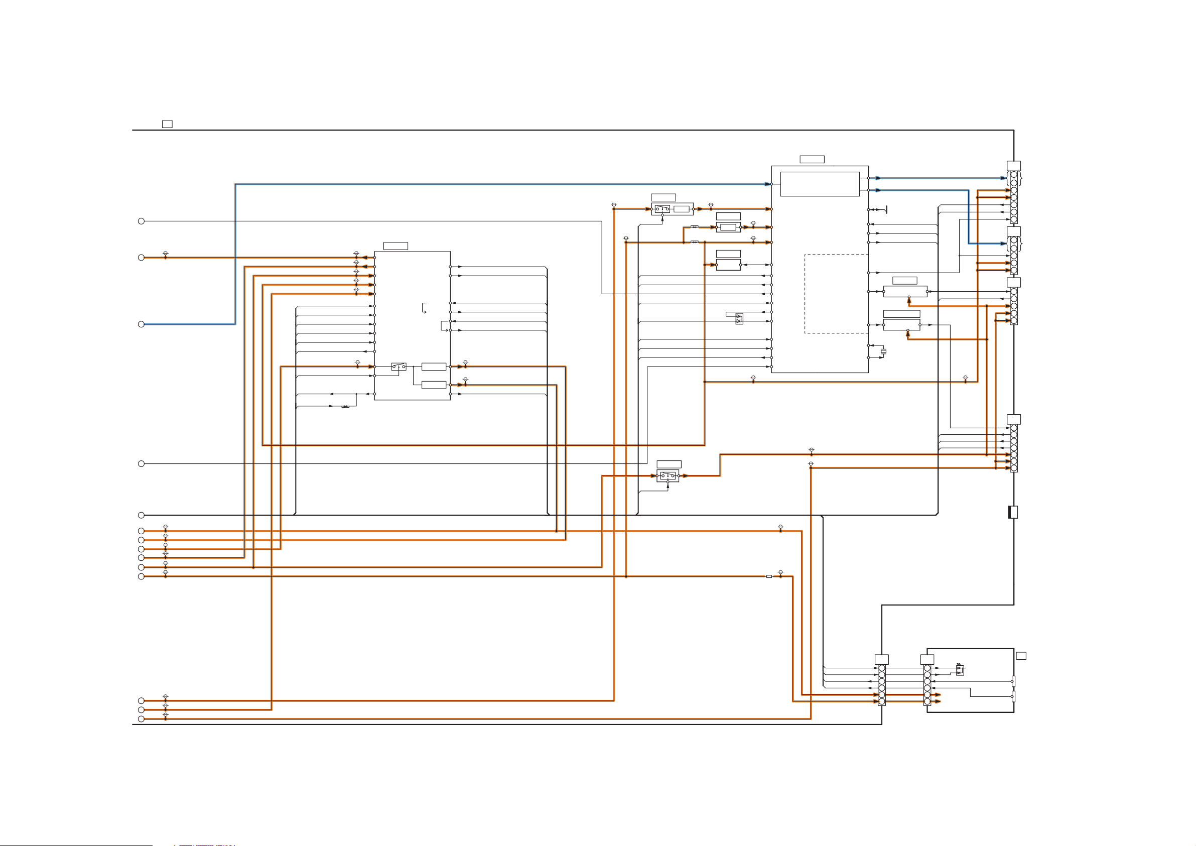
11.3. Block (2/4) Diagram
MAIN AV INPUT,PROCESSING
A
1
VDDSD18V33V
2
LVDS DATA
3
4
VDDSD18V33V
FFC_OFF_DET
SOS6_SC1
SOS7_SC2
SOS8_SS
SOS_DCC
PANEL_SOS
STB5V_SW_ON_A
POWER_DET
SW_OFF_DET
SUB9V
SUB5V
P+3.3V
VJ5000
F15V
STB5V
IC9300
PD6H
LVDS DATA
IC9803
IC9804
+1.2V
P+1.2V
P+5V
VJ9005
VJ9006
P+1.2V
IC9005
P+2.5V
+2.5V
P
P
IC9304
SPI
FLASH
P+3.3V
SI/SO
D9802
P+3.3V
DCDC15V
DCDCEN
SUB3.3V
IC5000
ANALOG-ASIC
SD_VCC
SUB9V
SUB5V
BUFF_EN
DTV_15V
FFC_OFF_DET
SOS6_SC1
(LED:6TIMES)
SOS7_SC2
(LED:7TIMES)
SOS8_SS
(LED:8TIMES)
SOS_DCC
(LED:9TIMES)
PANEL_SOS
S
POWER_DET
DTV_RST
DCDC_CTL
DRVRST_
IN
DRVRST_
OUT
UHZ
STB+1.1V
STB+3.3V
STBRST
STB1.1V
STB3.3V
DCDCEN
PDP_DRVRST
DRVRST
SC_UHZ
D_UHZ
XRSTSTM
XRST
P_S0
P_S1
DRVRST
PD6H_XRST_SYS
DISPEN
INIT_DONE
PLASMA AI
CPG
H/V Sync Control
Sub Filed Processor
1.2V
2.5V
3.3V
FLASH I/F
P_S0
P_S1
RF_LR
DRVRST
OFF_FLAG
XRST_SYS
DISPEN
LOGO_ON
INIT_DONE
P+15V DET
SOS_DCC
FFC_OFF_DET
DISCHARGE CONTROL
DATA DRIVER CONTROL
SUSTAIN CONTROL
SCAN CONTROL
P+5V
P+15V
VIDEO DATA
VIDEO DATA
D_UHZ
SOS_DCC
KEY1
KEY_POWER
IIC0
UHZ
FFC_OFF_DET
IC9402
SUSTAIN DATA
BUFFER
SOS8_SS
IC9400,01
SCAN DATA
BUFFER
X0LOGO_ON
X9300
20MHz
X1
P+3.3V
SC_UHZ
SOS6_SC1
SOS7_SC2
C11
A31
16
VIDEO DATA
54
1
P+3.3V
2
P+3.3V
4
KEYSCAN
5
KEY
DATA DRIVER CONTROL
A32
C21
2
VIDEO DATA
40
DATA DRIVER CONTROL
54
P+3.3V
55
P+3.3V
SS33
A33
SUSTAIN CONTROL
5
SOS8_SS
4
P+5V
2
P+15V
1
P+15V
SC20
A20
SCAN CONTROL
9
UHZ
3
SOS6_SC1
6
SOS7_SC2
1
P+5V
29
P+15V
30
P+15V
DCDCEN
CN0100
IIC0
D2820
IIC1
STM_IIC
SBO0/SBI0
G
R
5
STB3.3V
6
STB1.1V
7
STB5V
8
SUB9V
9
10
11
12
13
14
SUB5V
SUB3.3V
DCDC15V
F15V
P+15V
STB3.3V
SUB_AI3.3V
G_LED_ON
R_LED_ON
C.A.T.S
REMOTE_IN
A1
2
3
6
1
4
7
G_LED_ON
R_LED_ON
C.A.T.S
REMOTE_IN
STB3.3V
SUB_AI3.3V
K1
POWER LED
2
3
6
1
4
7
FOR
FACTORY
USE
POWER LED
K
REMOTE RECEIVER
C.A.T.S. SENSOR
SN2810
C.A.T.S SENSOR
RM2810
REMOTE
RECEIVER
37
Page 38
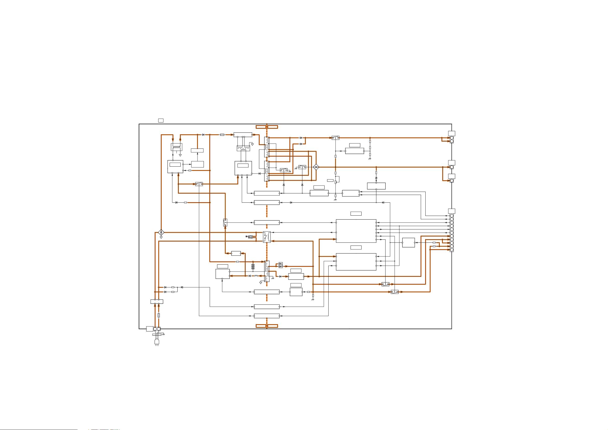
11.4. Block (3/4) Diagram
NEUTRAL
P9
P POWER SUPPLY
L100
L101
D100
D101
RECTIFIER
LF101
FILTER
LF102
**
F100
NO
HOLDER
LIVE
1
2
NPD
IC100
PFC
NP
NC
4
3
*2*
Q100
Q101
51
Q111
Q112
CONTROL
FET
DRIVER
Q307
D105,D113
D106,D116
F102
IC200
STB
CONTROL
Q107
Q300-Q303
RESONANCE
GD2
IC300
RESONANCE
CONTROL
VCC
Q202
+20V
SS
T300
GD1
RT
R100
**
HOT COLD
D302
OC
PC700
PHOTO COUPLER
PC400
PHOTO COUPLER
PC401
PHOTO COUPLER
RL100
1
*
23
D204
**
PC201
PHOTO COUPLER
PC200
PHOTO COUPLER
PC402
PHOTO COUPLER
T301
T302
T200
C25
P35
1
Vda
2
Vda
P2
1
Vsus
P11
1
Vsus
3
S0
2
S1
1
PANEL_MAIN_ON
4
SOS_P4
5
STB5V_SW_ON
7
TUNER_SUB_ON
6
STB5V
10
F15V
11
F15V
13
P+15V
15
SOUND+15V
SC2
SS11
A6P6
D700
D704
Vsus
VR251
Q600
PFC_ON/OFF
MAIN_RELAY_ON
VDD
VDD
AC_DET
VSUS_ON
IC600
Vda
ERROR DET
Q404,Q405
Vsus Adj
IC503
POWER MICOM
IC502
POWER MICOM
Q408,Q409
PANEL_MAIN_ON
SOS4_PS
STB5V_SW_ON
F_STB_ON
P+15V_ON
F15V_ON
POWER_SOS
P+15V_ON
SOS4_PS
(LED:4TIMES)
Vsus
ERROR DET
Q500
Q502
Vda
Vsus
Q503,Q504
P+15V
ERROR
DET
STB5V
F15V
+15V
D600
D601
Q701
Q415
Q416
Q702
IC700
Vsus
ERROR DET
PFC_ON/OFF
4
D501
IC501
D505
STB+5V
IC400
F_STBY
ERROR
DET
AC DET
VSUS_ON
COLDHOT
AC CORD
38
Page 39
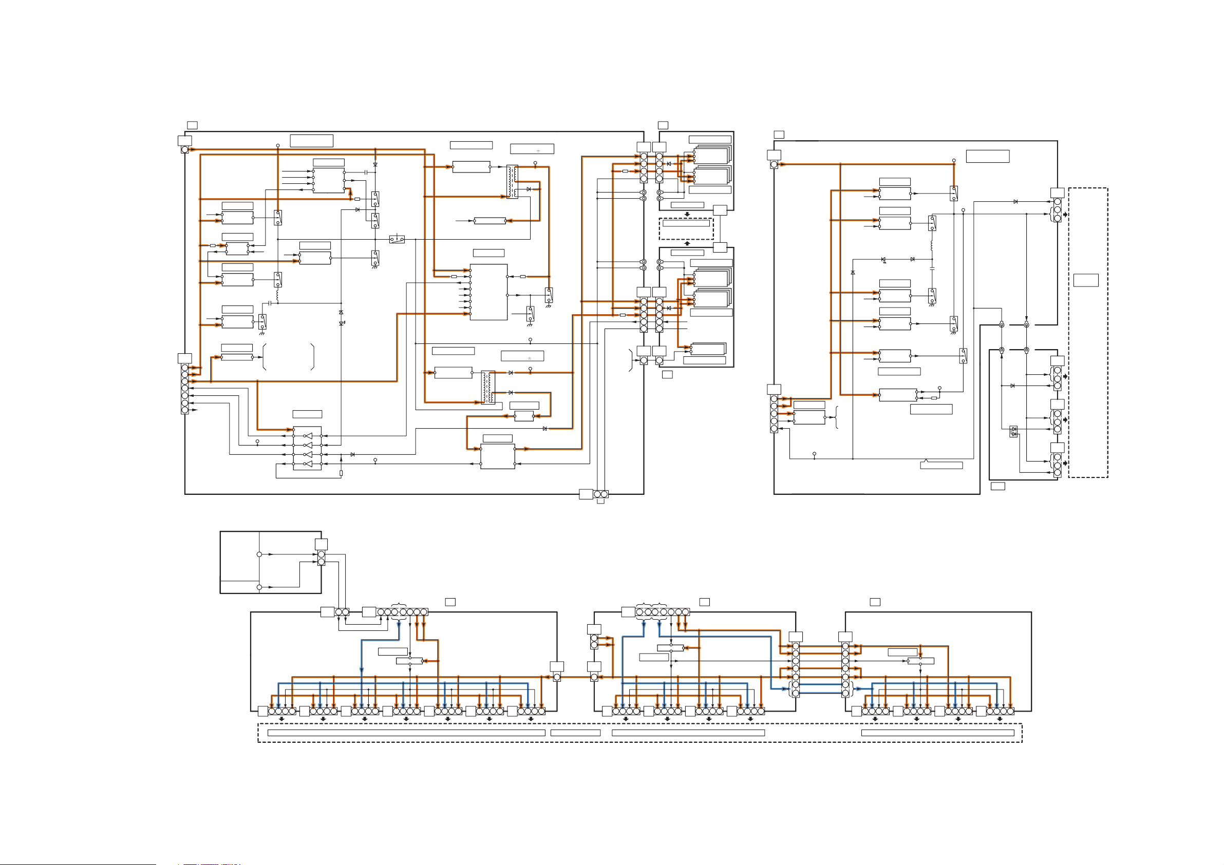
11.5. Block (4/4) Diagram
SC
SCAN DRIVE
P2
SC2
1
Vsus
IC16501
CMH
BUFFER
SUSTAIN H
IC16603
CSH
AND
IC16502
CSH
BUFFER
RECOVERY H
IC16522
CSL
BUFFER
RECOVERY L
SCAN CONTROL
A20
P+15V
P+15V
P+5V
SOS6
SOS7
SC
20
2
1
30
22
UHZ
28
25
SCAN
CONTROL
IC16561
BUFFER
(LED:6TIMES)
TPVSUS
Q16451
Q16452
CMH
CML
CSH
CSL
CPH
CIS NCVSET2
TPSOS6
ERM
CELR
CEL
NCRC1
NCRC2
NCEL
CPH
NCVSET2
CSH
NCPH
Q16402
Q16403
CML
Q16441
Q16442
Reference Voltage
Vsus Lo : 213V
Vsus Hi : 218V
VOL
IC16521
BUFFER
SUSTAIN L
SIU
OC1
OC2
CLK
SEL
IC16563
INVERTER
IC16600
BUFFER
D16583
LED(G)
D16477
Q16422
Q16424
UHZ
(LED:7TIMES)
D16618
Q16600
Q16601
TPSOS7
CIS
Q16621
Q16622
Q16623
Q16624
SEPA
SU
SCAN OUT (UPPER)
ZA14901
ZA14902
SU1-SU5
PLASMA PANEL
PANEL SCAN
ELECTRODE
SD1-SD5
ZA14951
ZA14952
IC14901,02
SD
SCAN OUT (LOWER)
IC14601-03
PDP SCAN
DRIVER
PDP SCAN
DRIVER
IC14604-06
IC14801-03
PDP SCAN
DRIVER
PDP SCAN
DRIVER
IC14804-06
SCN_PRO
CHA
LOGIC IC
SU
11
SD
11
IC16784,85
PC16897
IPD CIRCUIT
VAD GEN.
SHUNT REG
CELR
Q16646
Q16647
Q16660
Reference Voltage
Vad = 200
T16471
5V
TPVAD
VAD2
F5V
VSCN-F
VFO
VFG
ZA16411
ZA16412
SC
SU
41
41
2
66
8
1
2
8
1
VAD RECOVERY
VFG
CEL
NCRC1
NCRC2
NCVSET2
IC16786,87
PC16723
IPD CIRCUIT
VSCN GEN.
SHUNT REG
IC16921
IGBT CONTROL
VFG
T16472
NCEL
Reference Voltage
Vscn = 147
D16713
D16714
D16728
TPVFG
TPSC1
VAD
Q16661
Q16820
3V
VSCN-F
F5V
VSCN_F
VFO
VHIZ
SIU
OC1
OC2
CLK
SEL
ZA16421
ZA16422
SC
SD
42
42
6
6
2
2
1
1
8
8
9
9
SC
SD
46
46
IC16795
F15V
D16825
SUSTAIN CONTROL
IC16725
F5V
MAIN_STOP0
SCN_PRO
VFG
CHA
SC
2
1
50
SC JIG
P11
A33
P+15V
P+15V
SOS8_SS
Vsus
P+5V
SS
SS
11
1
SS
33
19
20
17
16
SUSTAIN DRIVE
IC16241
BUFFER
TPSOS8
(LED:8TIMES)
UEH
USL
USH
UML
UMH
D16255
UMH
USH
USL
UML
UEH
MAIN H
IC16131
BUFFER
IC16151
BUFFER
RECOVERY H
D16254A
LED(G)
RECOVERY L
IC16152
BUFFER
IC16132
BUFFER
MAIN L
PC16191
BUFFER
IC16304,12
PC16301
IPD CIRCUIT
VE GEN.
SHUNT REG
Q16002
Q16004
Q16041
MID
Q16051
Q16053
Q16021
Q16022
Q16024
TPVE
Reference Voltage
Ve = 170V
FPC PROTECTOR
Q16101
Q16102
TPVSUS
TPSS1
Reference Voltage
Vsus Lo : 213V
Vsus Hi : 218V
SUSOUT
SS2
D16286
ZA16106
ZA16116
D16352
D16351
SUSTAIN OUT
(LOWER)
ZA16101
ZA16111
SS
52
1
2
13
PLASMA
PANEL
PANEL
SUSTAIN
ELECTRODE
SS
54
2
13
1
SS
55
2
13
1
SS
57
2
13
1
CONTROL UNIT ASSY
OPERATION
KEYS
POWER SW
CB1
KEY3
352
C14
CB2 CB3
KEYSCAN
2
A31
C11
VIDEO DATA
CONTROL DATA
KEYSCAN
KEY3
2
55
40 1
51
IC17101
BUFFER
CB4
DATA DRIVER
P+3.3V
54
P+3.3V
CB5
C1
C25
P35
1
VDA
2
VDA
CB6
C10
1
CB7
C20
VDA
1
CB8
PLASMA PANEL
VIDEO DATA
A32
C21
VIDEO DATA
54
34
16
36
BUFFER
IC17201
CB9
DATA DRIVER
P+3.3V
P+3.3V
CONTROL DATA
2
CB
10
C2
DATA DRIVER (CENTER)DATA DRIVER (RIGHT)
C26
31
32
CONTROL DATA
36
40
VIDEO DATA
11
VIDEO DATA
29
CB
11
P+3.3V
P+3.3V
C36
VDA
VDA
C3
DATA DRIVER (LEFT)
10
9
5
1
30
12
CB
12
IC17301
CB
13
BUFFER
CB
14
CB
15
DATA DRIVER
39
Page 40

40
Page 41
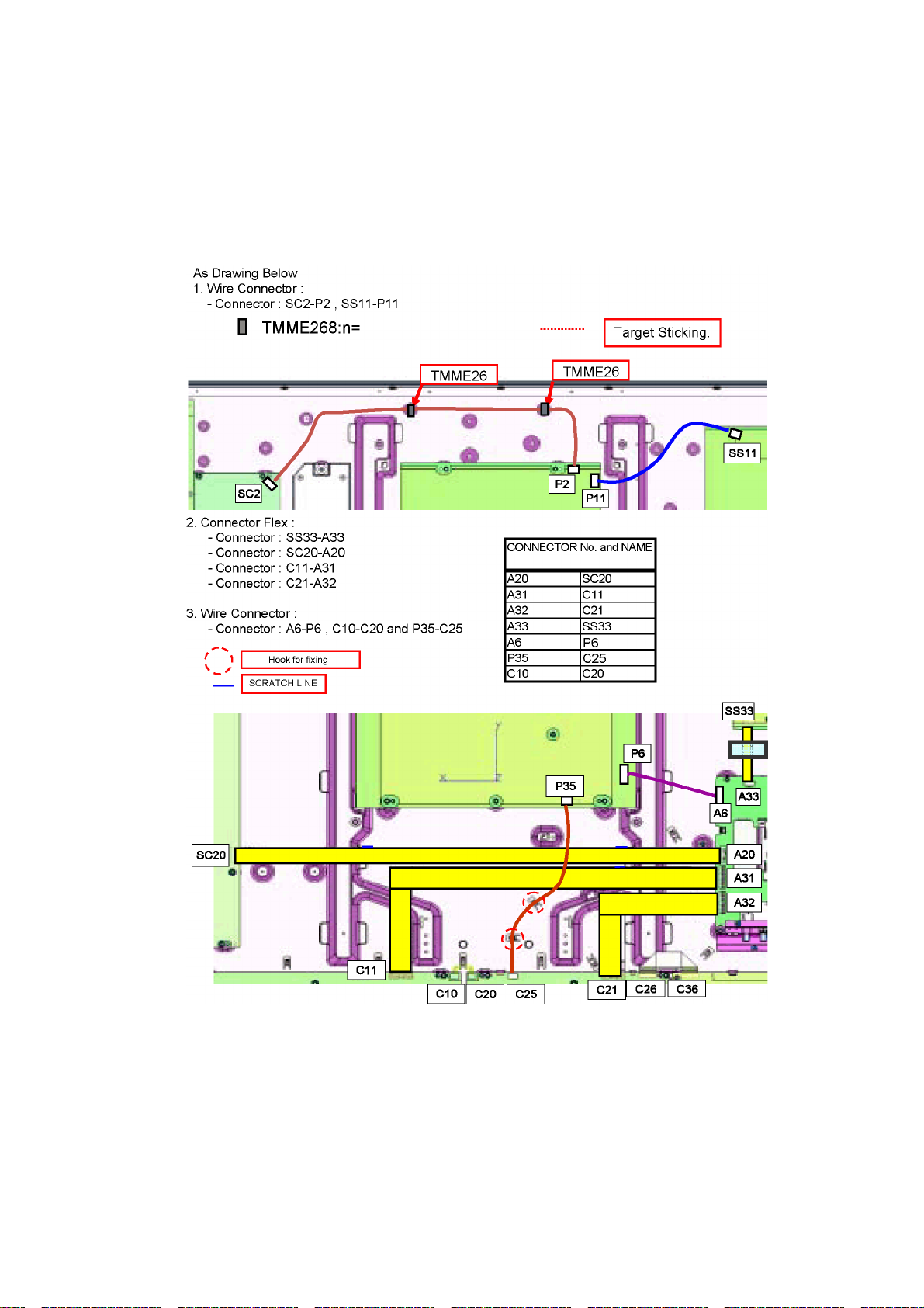
12 Wiring Connection Diagram
12.1. Caution statement.
Caution:
Please confirm that all flexible cables are assembled correctly.
Also make sure that they are locked in the connectors.
Verify by giving the flexible cables a very slight pull.
12.2. Wiring (1)
41
Page 42
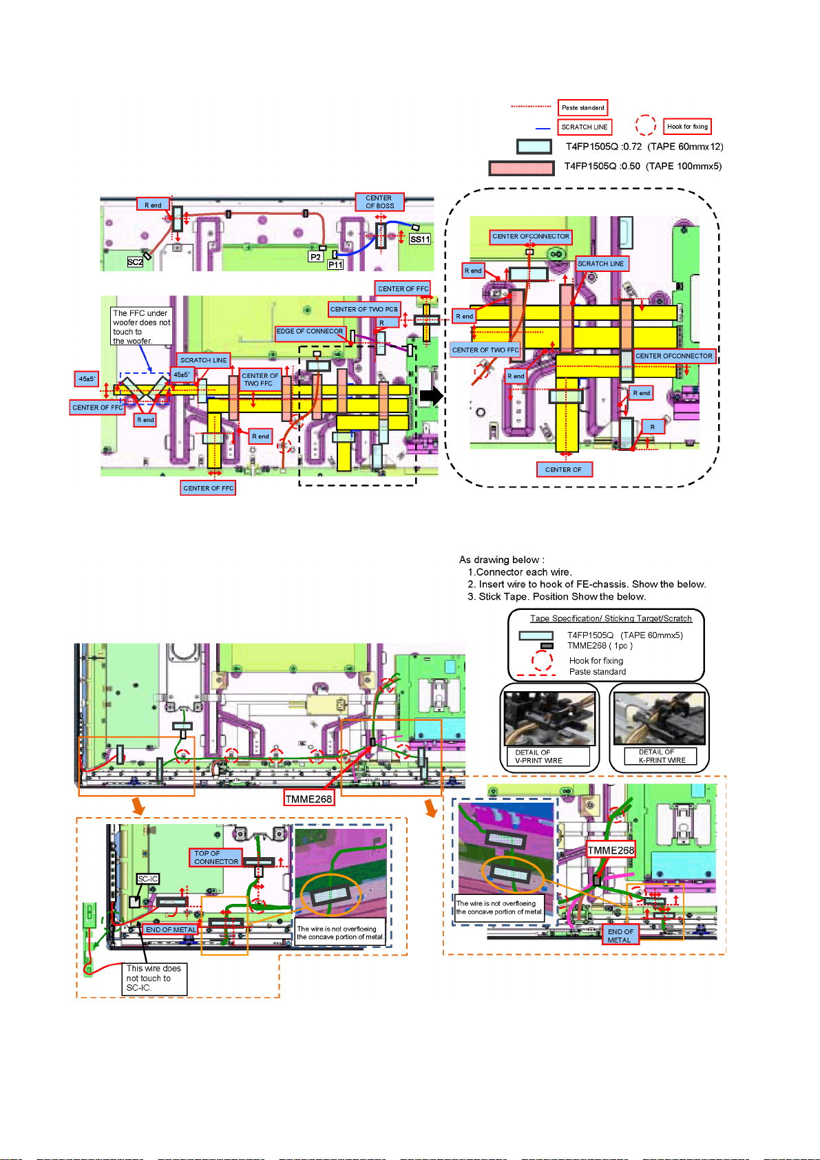
12.3. Wiring (2)
12.4. Wiring (3)
42
Page 43
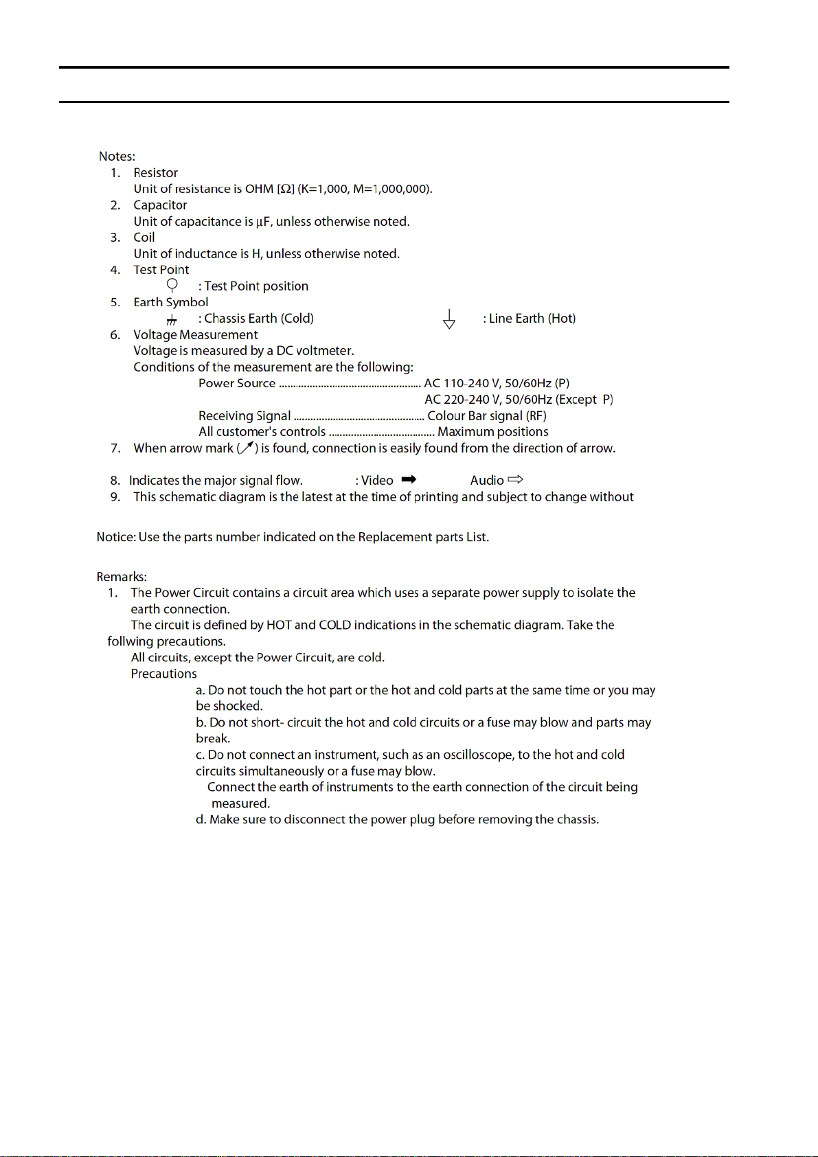
Model No. : TH-P50ST50A/D/G/K/M/P/S/T/V/Z Schematic Diagram Note
S-1
Page 44
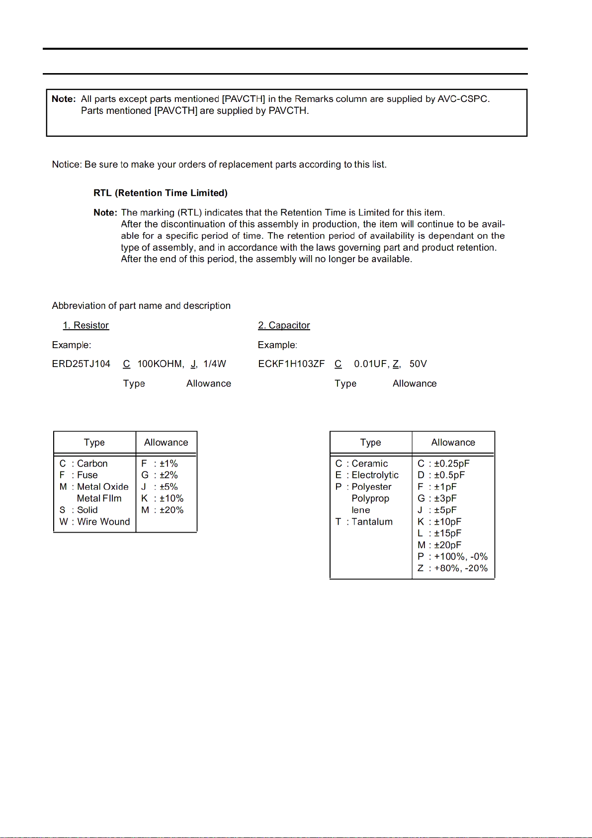
Model No. : TH-P50ST50A/D/G/K/M/P/S/T/V/Z Replacement Parts List Note
S-2
Page 45
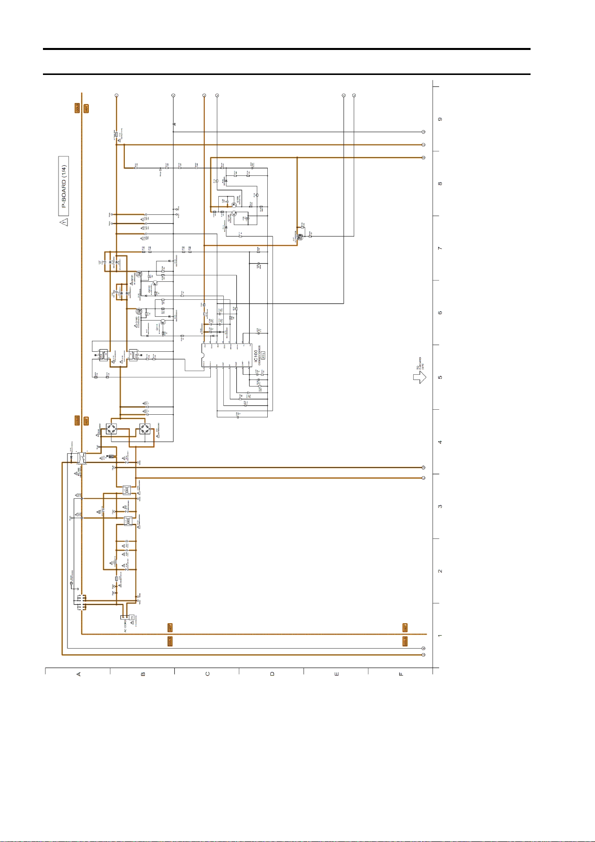
Model No. : TH-P50ST50A/D/G/K/M/P/S/T/V/Z P-Board (1/4)
S-3
Page 46
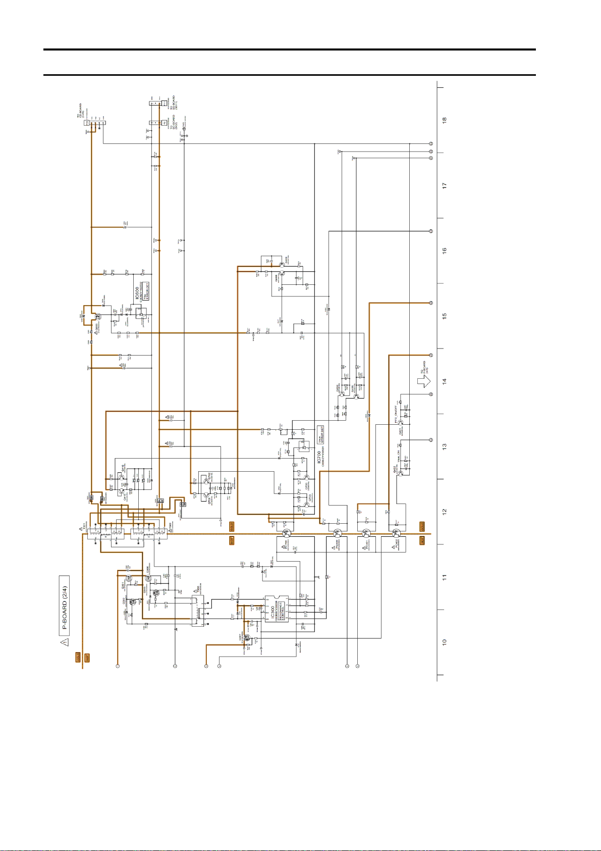
Model No. : TH-P50ST50A/D/G/K/M/P/S/T/V/Z P-Board (2/4)
S-4
Page 47
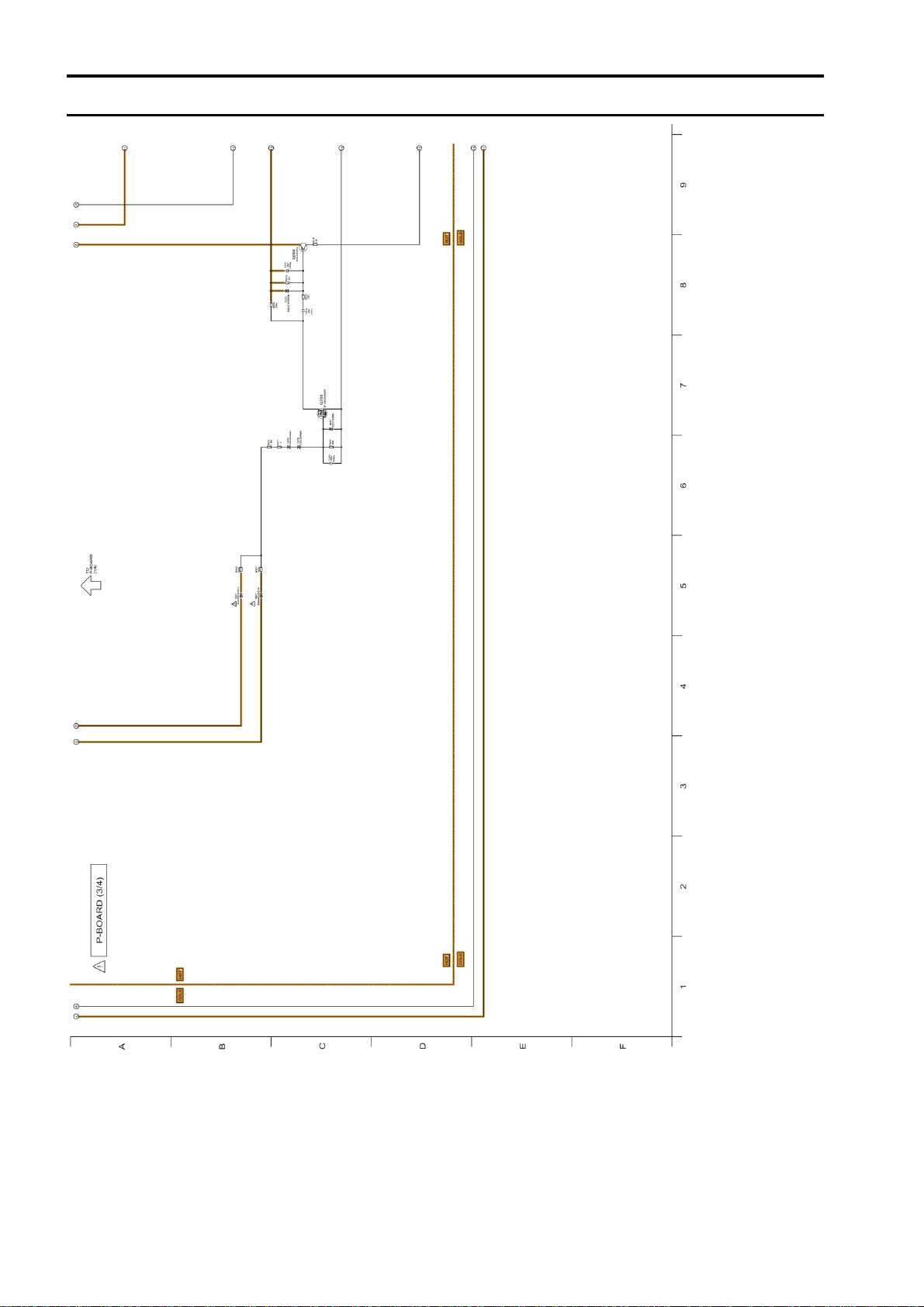
Model No. : TH-P50ST50A/D/G/K/M/P/S/T/V/Z P-Board (3/4)
S-5
Page 48
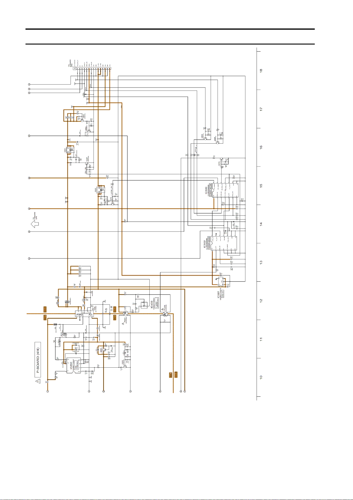
Model No. : TH-P50ST50A/D/G/K/M/P/S/T/V/Z P-Board (4/4)
S-6
Page 49
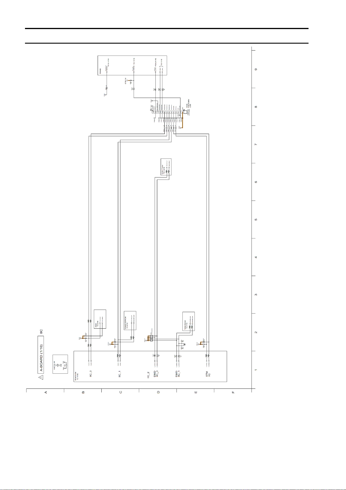
Model No. : TH-P50ST50A/D/G/K/M/P/S/T/V/Z A-Board (1/16)
S-7
Page 50
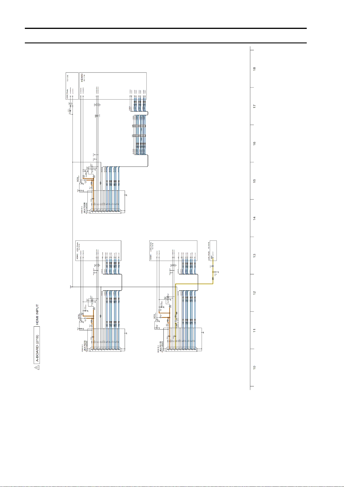
Model No. : TH-P50ST50A/D/G/K/M/P/S/T/V/Z A-Board (2/16)
S-8
Page 51
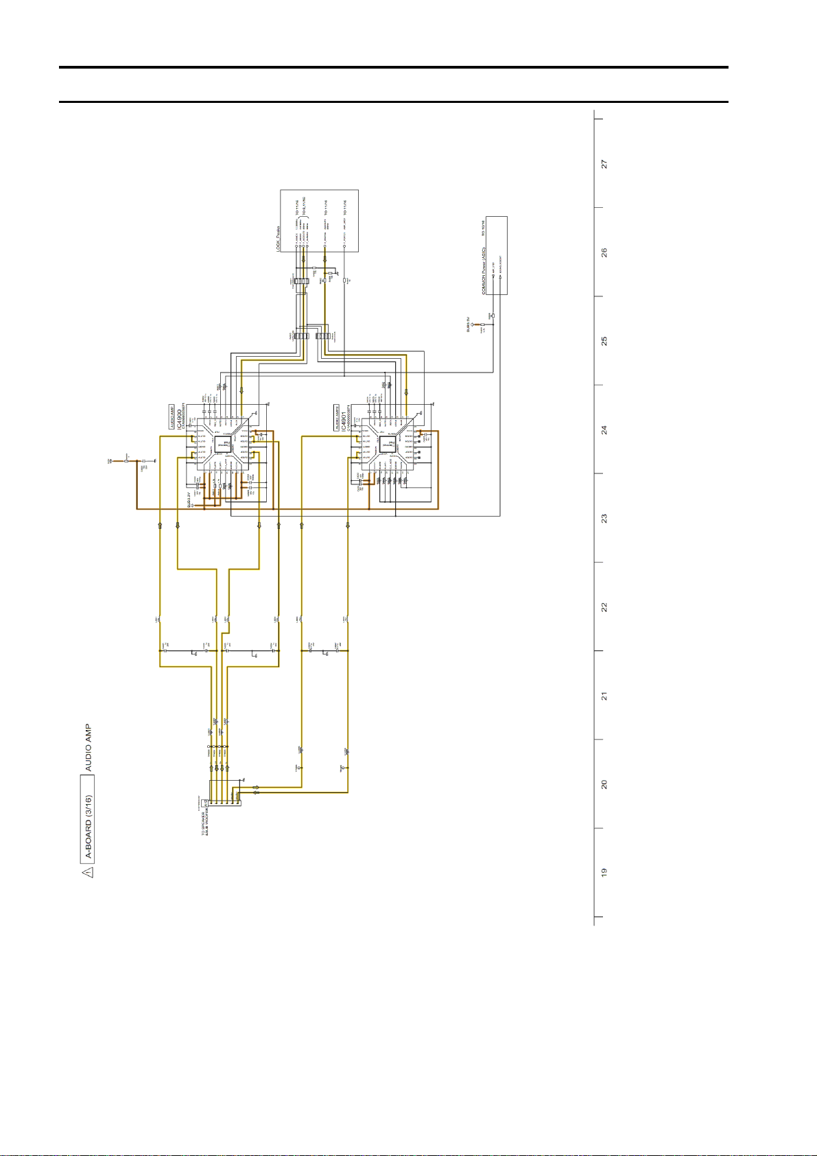
Model No. : TH-P50ST50A/D/G/K/M/P/S/T/V/Z A-Board (3/16)
S-9
Page 52
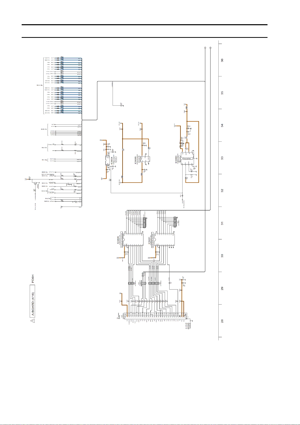
Model No. : TH-P50ST50A/D/G/K/M/P/S/T/V/Z A-Board (4/16)
S-10
Page 53
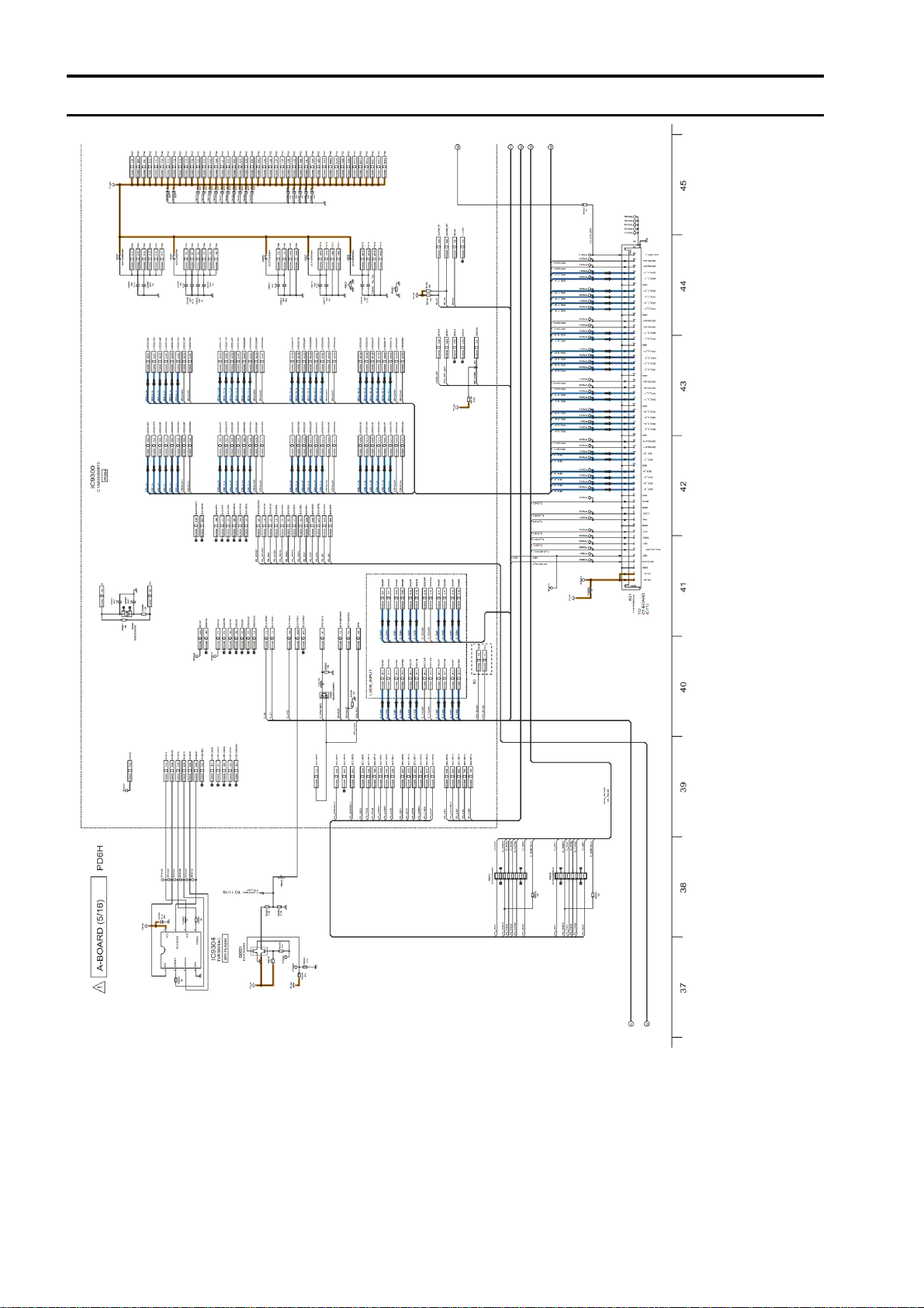
Model No. : TH-P50ST50A/D/G/K/M/P/S/T/V/Z A-Board (5/16)
S-11
Page 54
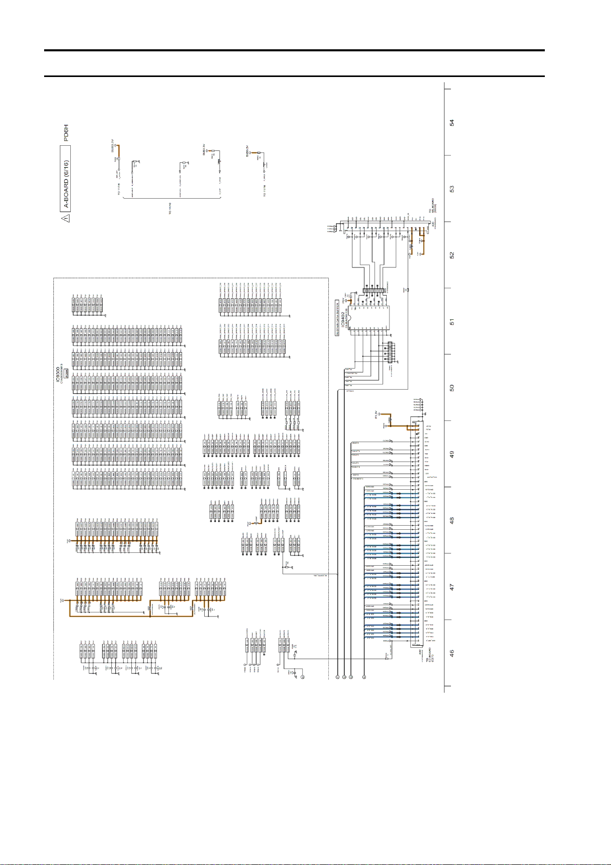
Model No. : TH-P50ST50A/D/G/K/M/P/S/T/V/Z A-Board (6/16)
S-12
Page 55
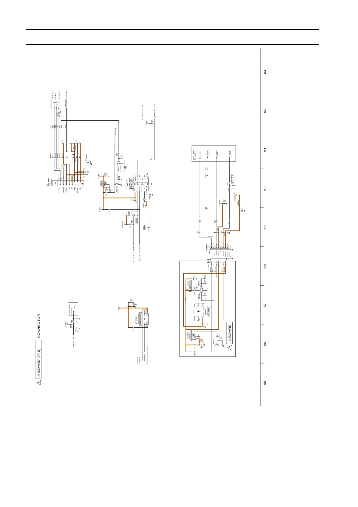
Model No. : TH-P50ST50A/D/G/K/M/P/S/T/V/Z A-Board (7/16) and K-Board
S-13
Page 56
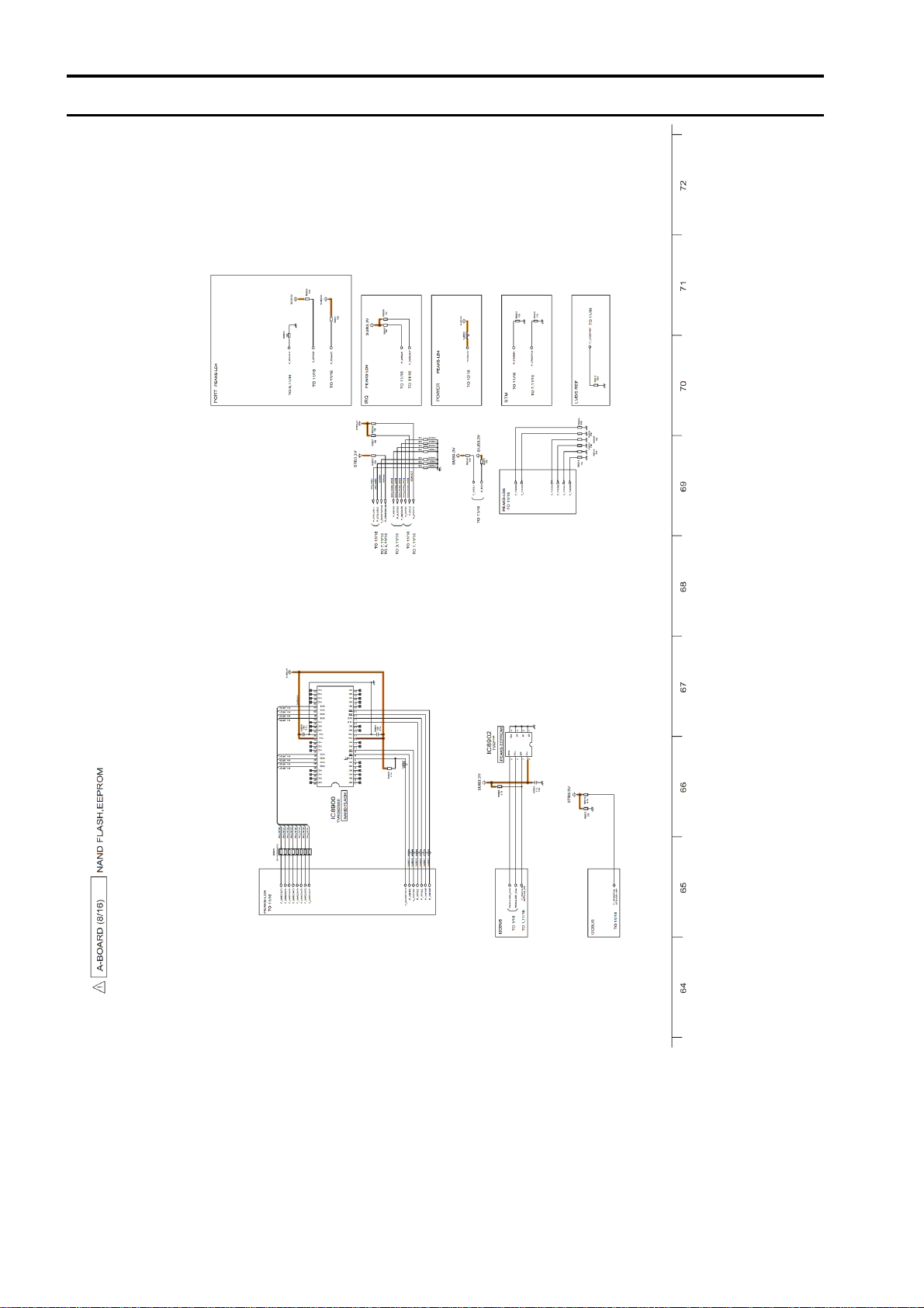
Model No. : TH-P50ST50A/D/G/K/M/P/S/T/V/Z A-Board (8/16)
S-14
Page 57
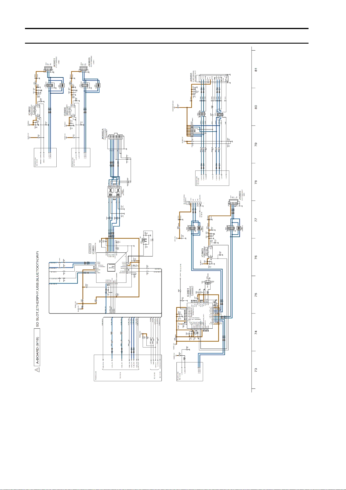
Model No. : TH-P50ST50A/D/G/K/M/P/S/T/V/Z A-Board (9/16)
S-15
Page 58
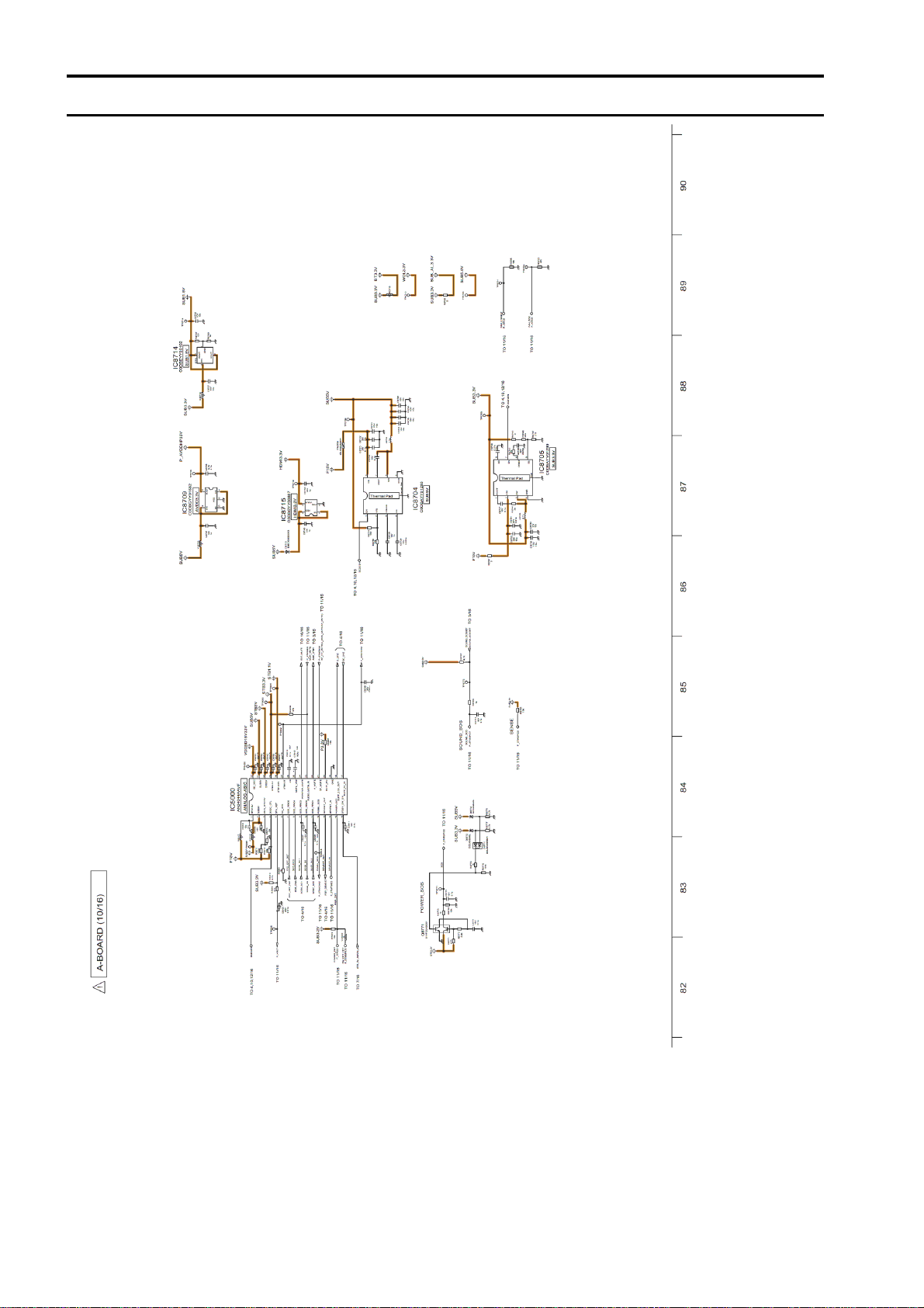
Model No. : TH-P50ST50A/D/G/K/M/P/S/T/V/Z A-Board (10/16)
S-16
Page 59
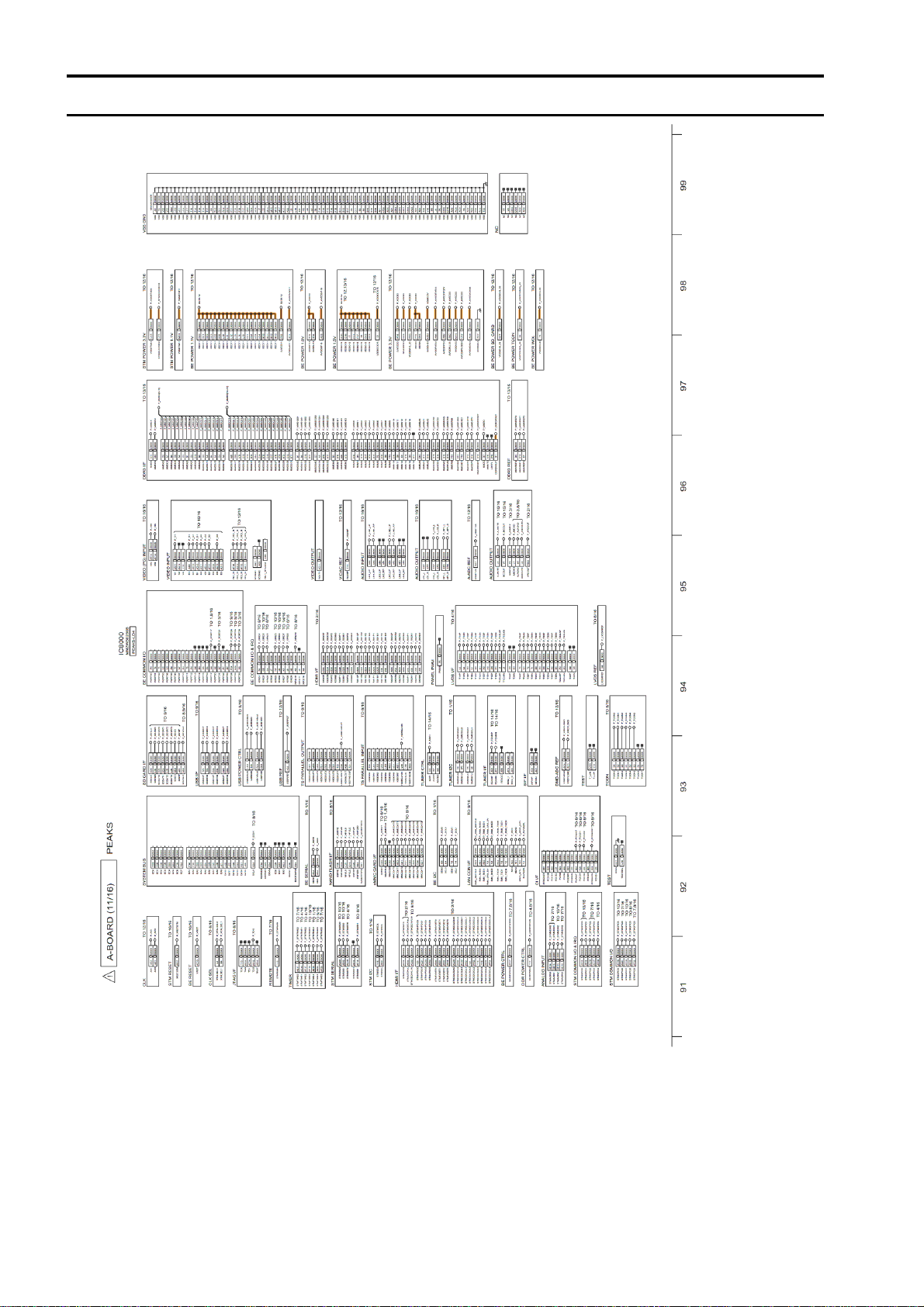
Model No. : TH-P50ST50A/D/G/K/M/P/S/T/V/Z A-Board (11/16)
S-17
Page 60
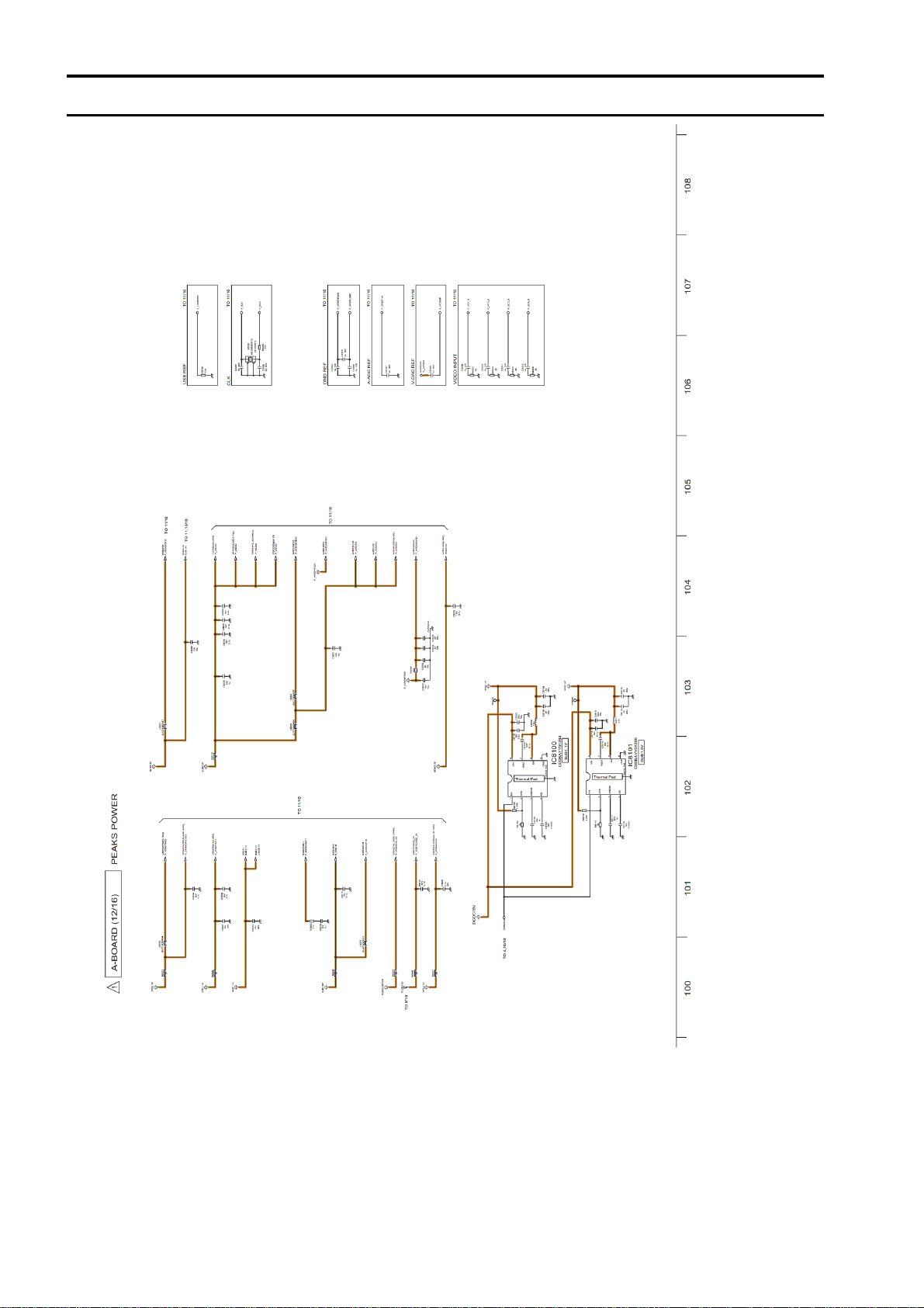
Model No. : TH-P50ST50A/D/G/K/M/P/S/T/V/Z A-Board (12/16)
S-18
Page 61
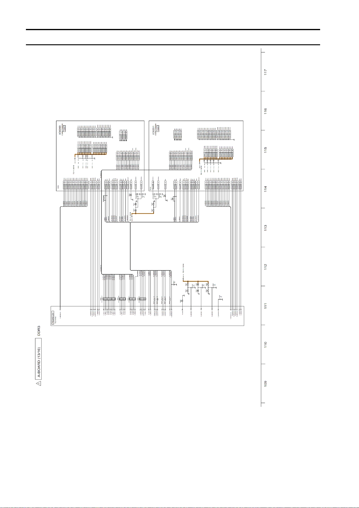
Model No. : TH-P50ST50A/D/G/K/M/P/S/T/V/Z A-Board (13/16)
S-19
Page 62
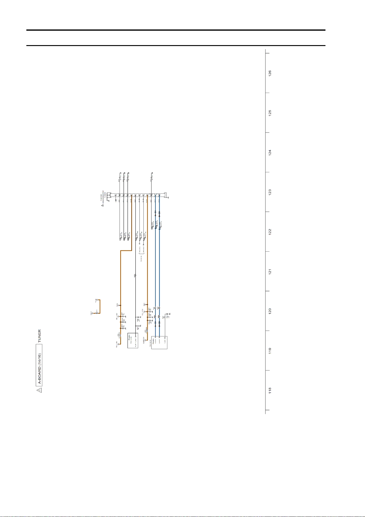
Model No. : TH-P50ST50A/D/G/K/M/P/S/T/V/Z A-Board (14/16)
S-20
Page 63
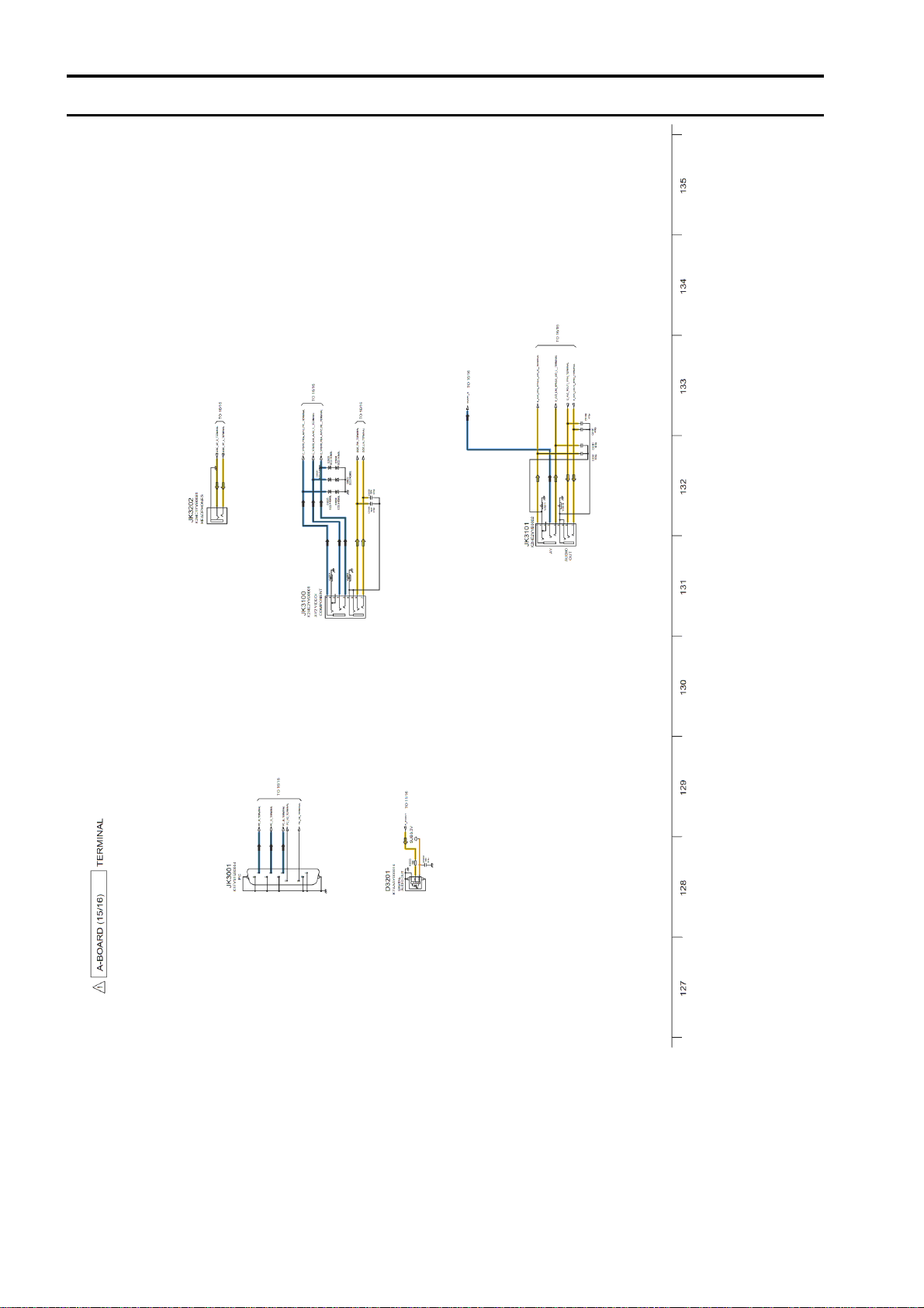
Model No. : TH-P50ST50A/D/G/K/M/P/S/T/V/Z A-Board (15/16)
S-21
Page 64
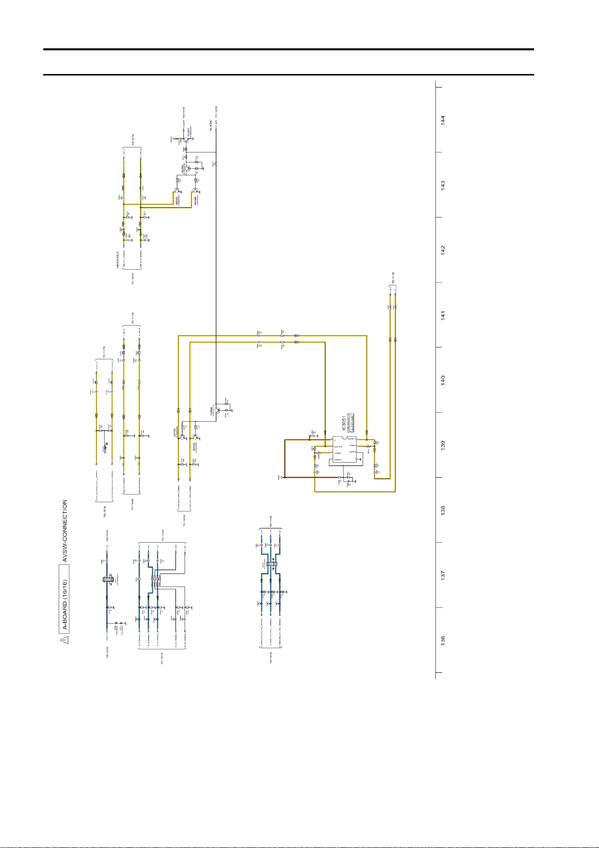
Model No. : TH-P50ST50A/D/G/K/M/P/S/T/V/Z A-Board (16/16)
S-22
Page 65
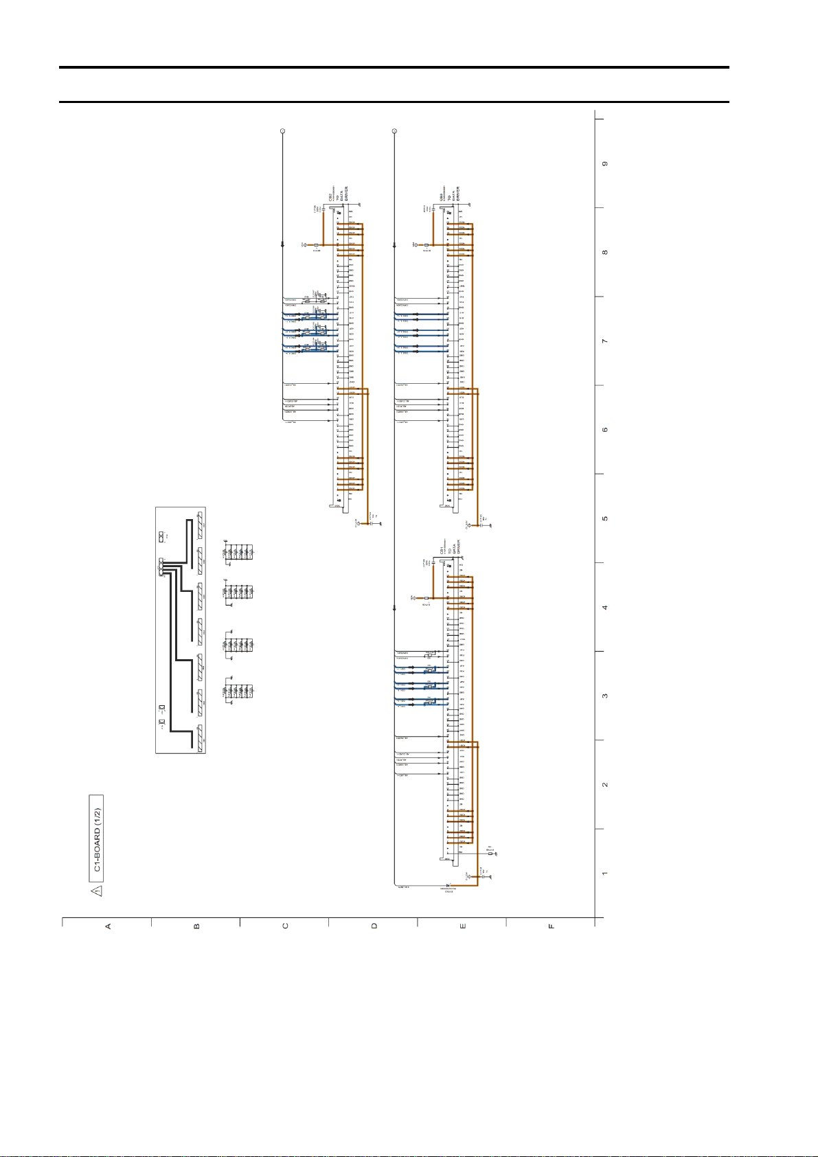
Model No. : TH-P50ST50A/D/G/K/M/P/S/T/V/Z C1-Board (1/2)
S-23
Page 66
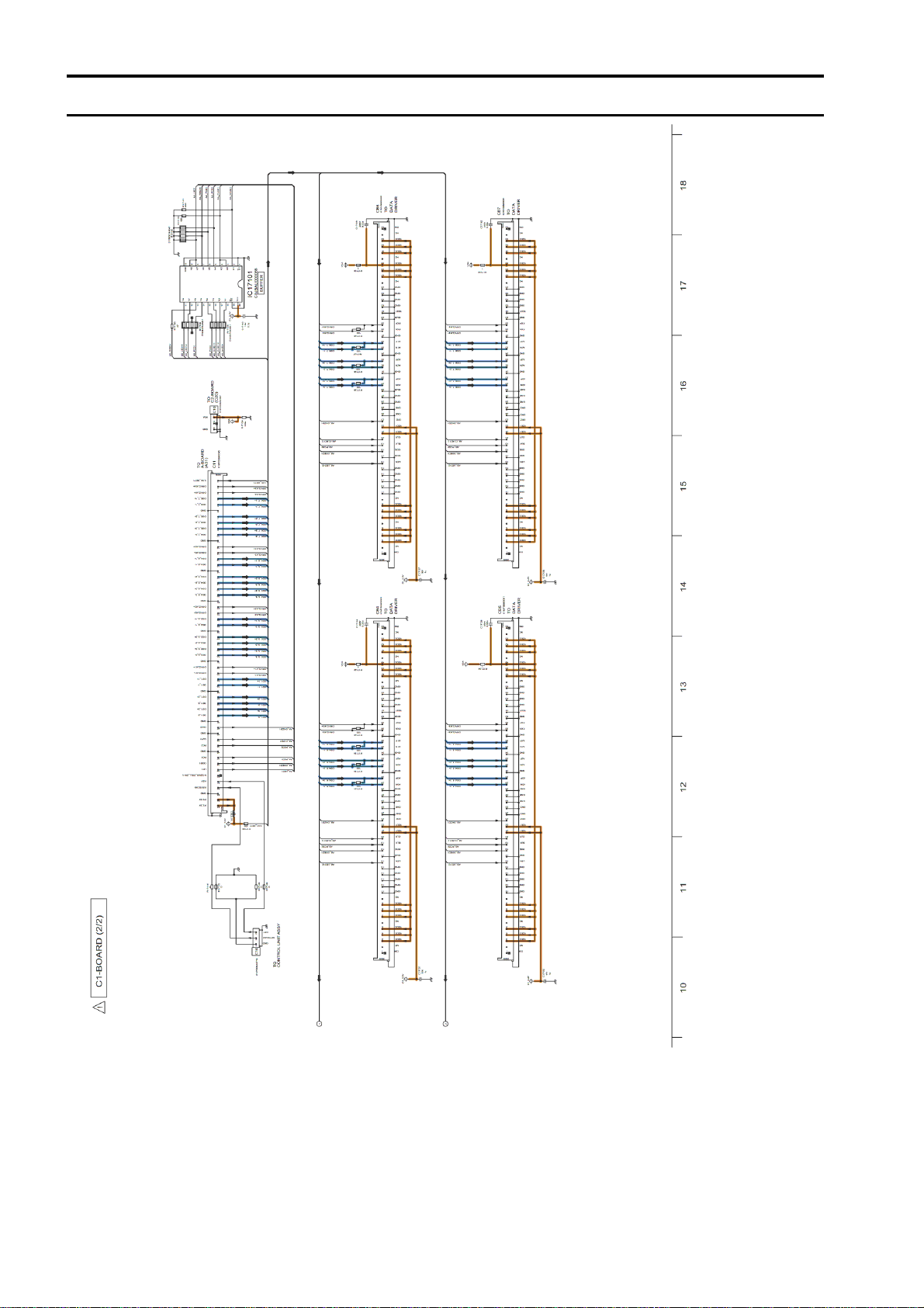
Model No. : TH-P50ST50A/D/G/K/M/P/S/T/V/Z C1-Board (2/2)
S-24
Page 67
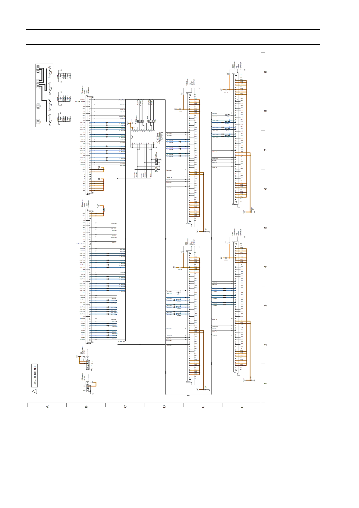
Model No. : TH-P50ST50A/D/G/K/M/P/S/T/V/Z C2-Board
S-25
Page 68
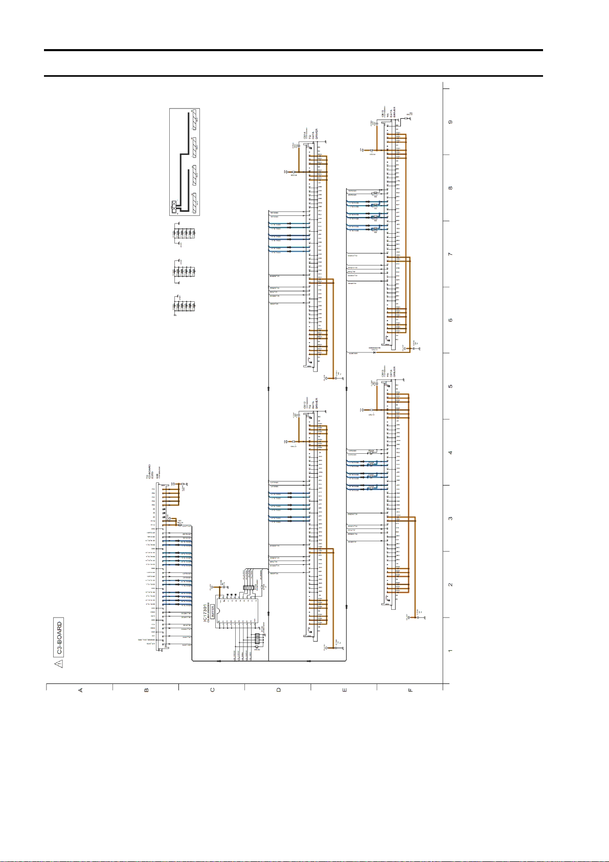
Model No. : TH-P50ST50A/D/G/K/M/P/S/T/V/Z C3-Board
S-26
Page 69
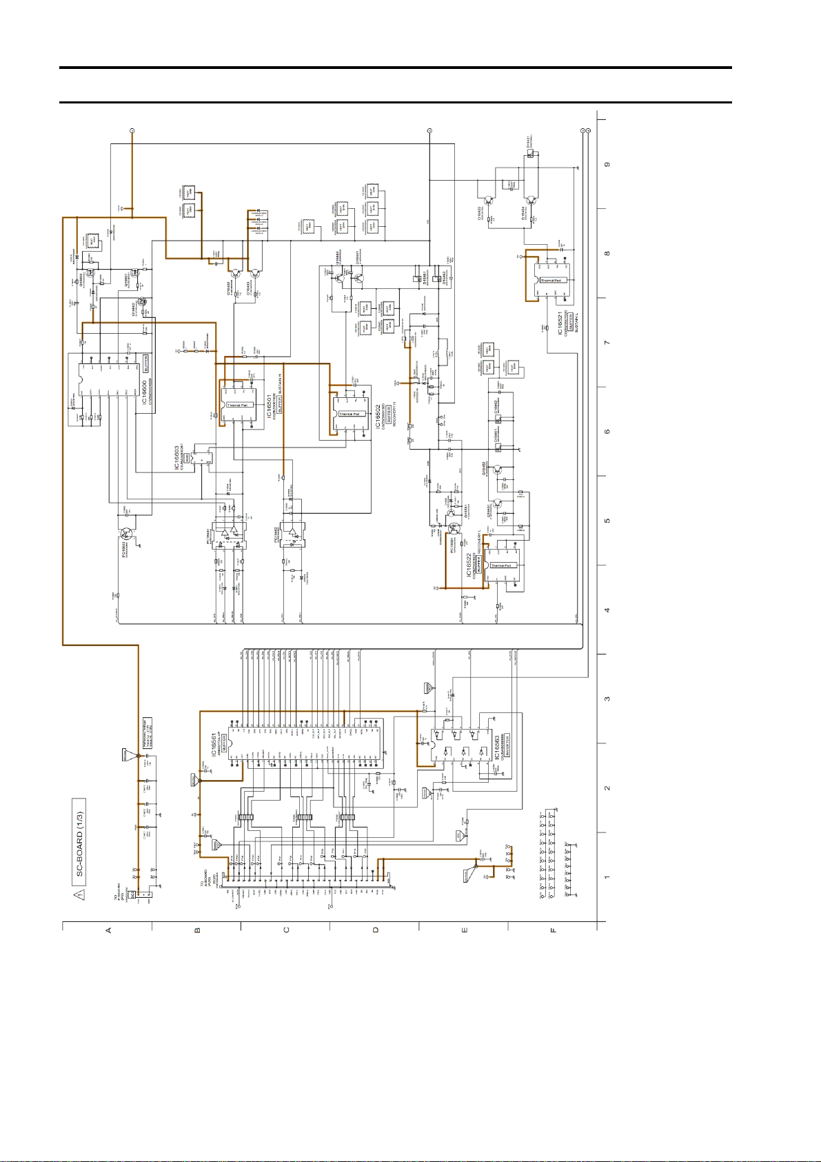
Model No. : TH-P50ST50A/D/G/K/M/P/S/T/V/Z SC-Board (1/3)
S-27
Page 70
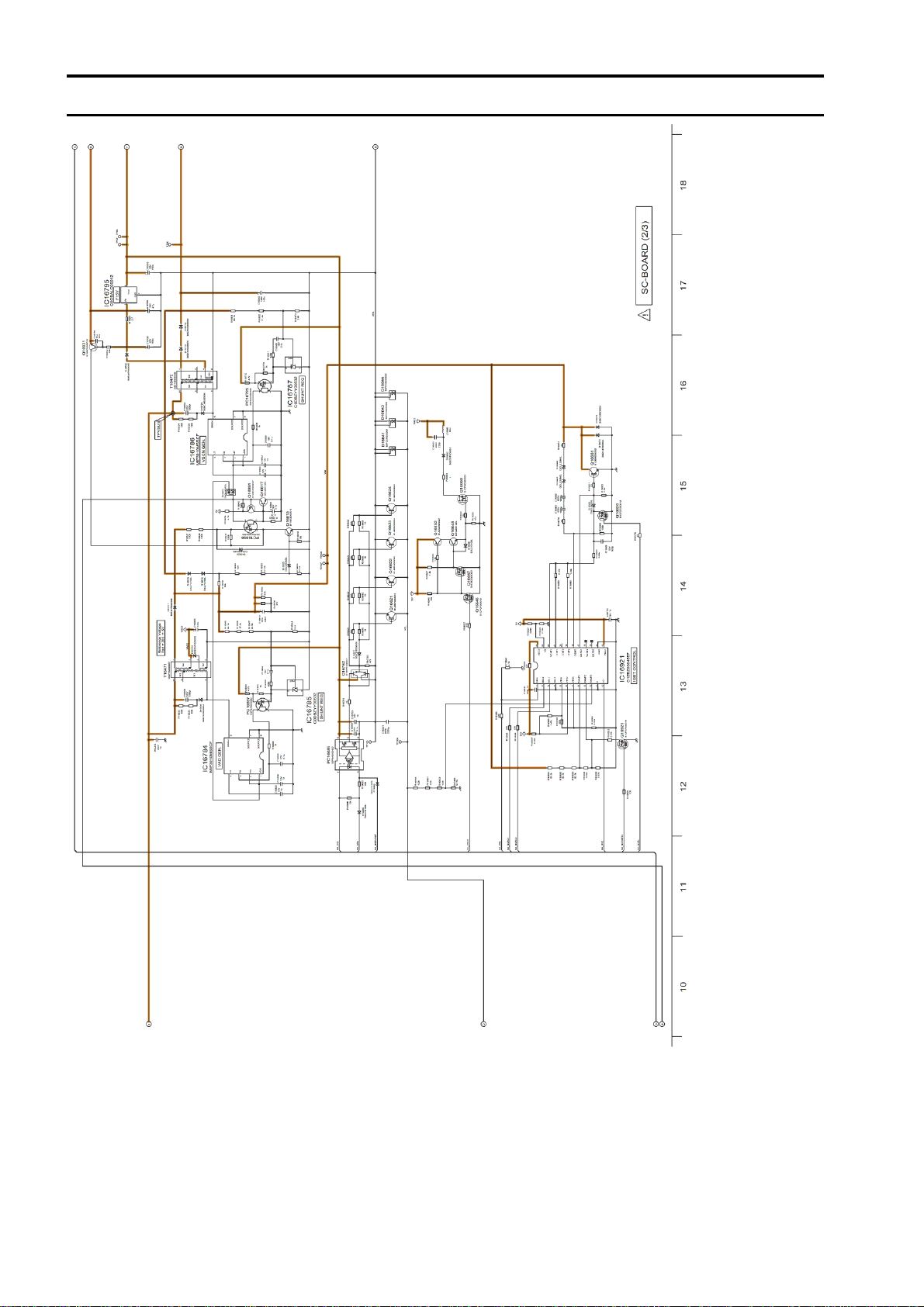
Model No. : TH-P50ST50A/D/G/K/M/P/S/T/V/Z SC-Board (2/3)
S-28
Page 71
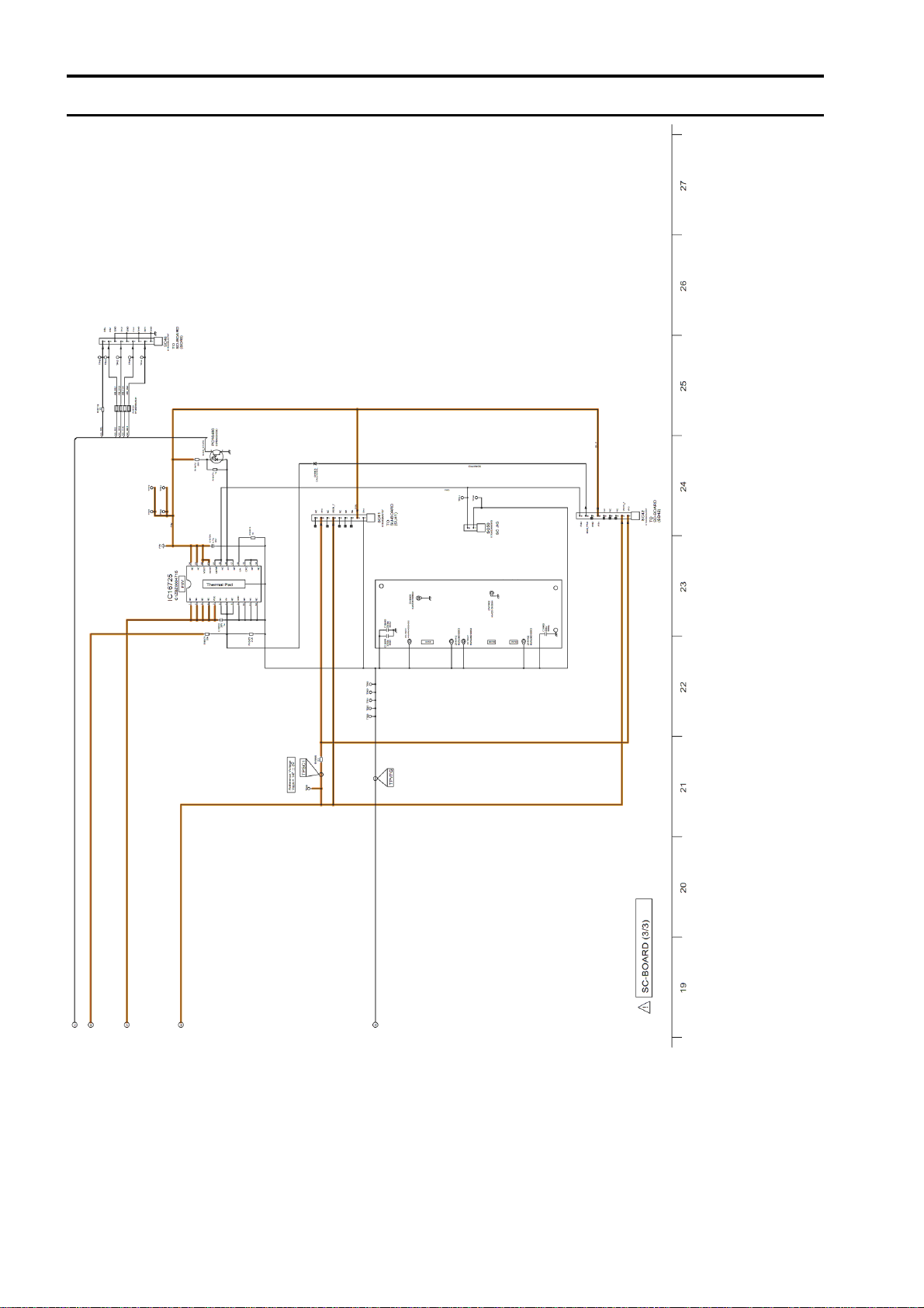
Model No. : TH-P50ST50A/D/G/K/M/P/S/T/V/Z SC-Board (3/3)
S-29
Page 72
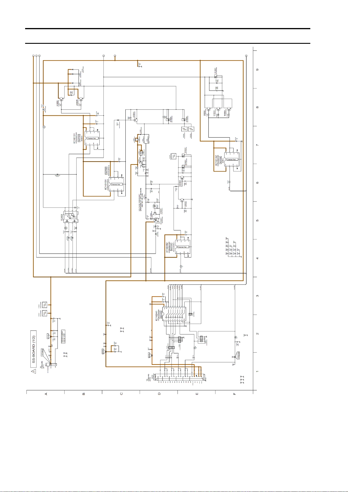
Model No. : TH-P50ST50A/D/G/K/M/P/S/T/V/Z SS-Board (1/2)
S-30
Page 73
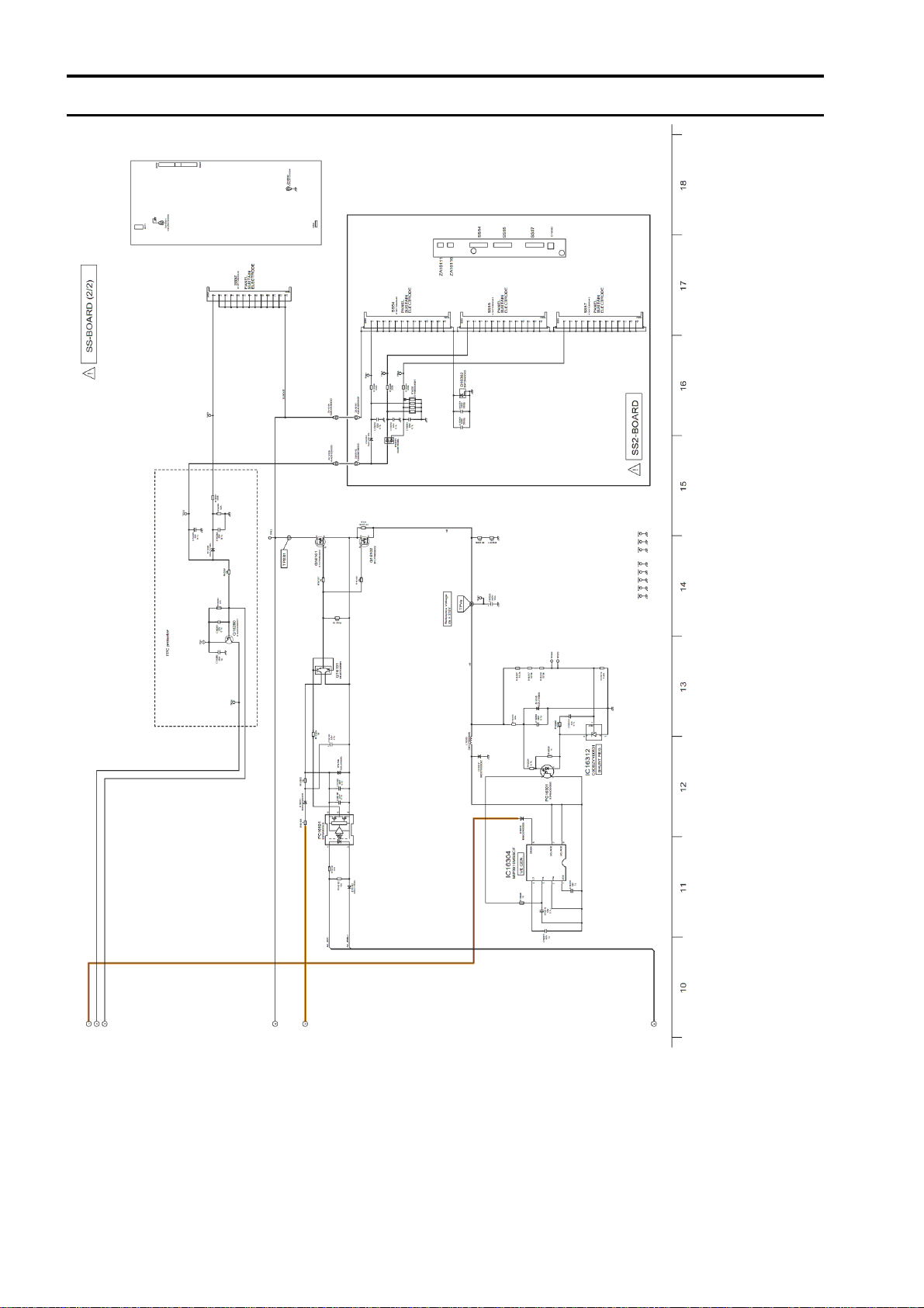
Model No. : TH-P50ST50A/D/G/K/M/P/S/T/V/Z SS-Board (2/2) and SS2-Board
S-31
Page 74
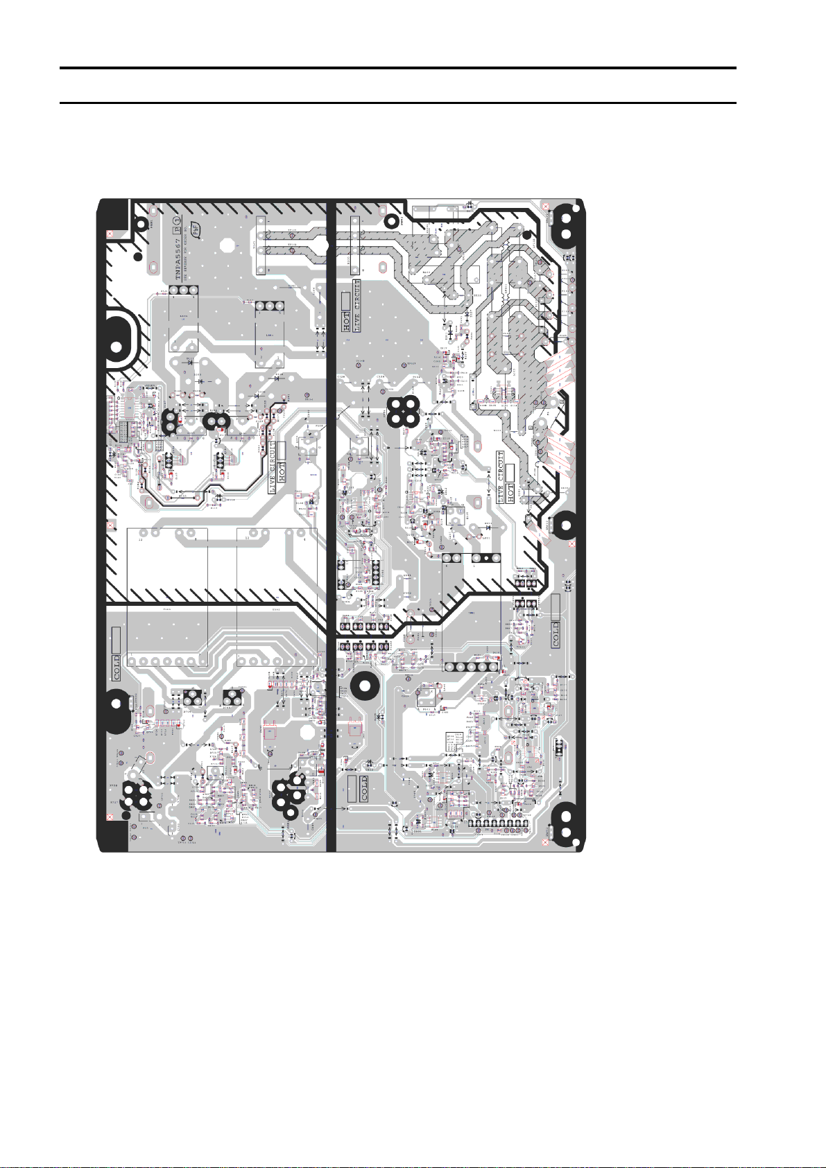
Model No. : TH-P50ST50A/D/G/K/M/P/S/T/V/Z P-Board (Foil Side)
S-32
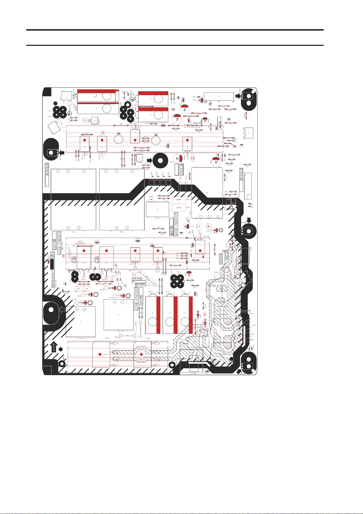
Page 75
Model No. : TH-P50ST50A/D/G/K/M/P/S/T/V/Z P-Board (Component Side)
S-33
Page 76
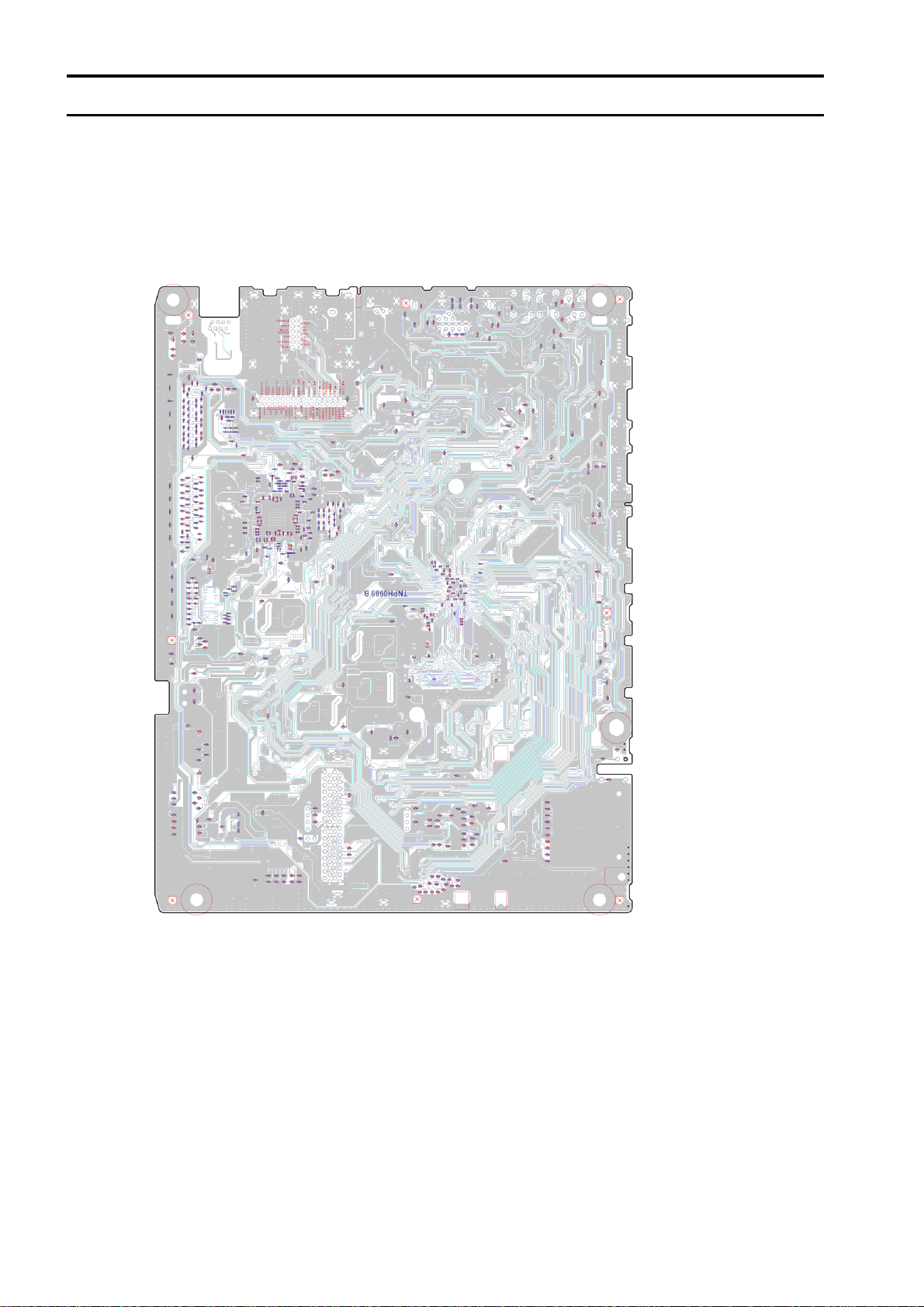
Model No. : TH-P50ST50A/D/G/K/M/P/S/T/V/Z A-Board (Foil Side)
S-34
Page 77
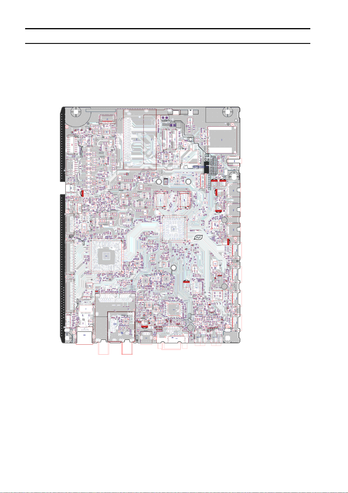
Model No. : TH-P50ST50A/D/G/K/M/P/S/T/V/Z A-Board (Component Side)
S-35
Page 78
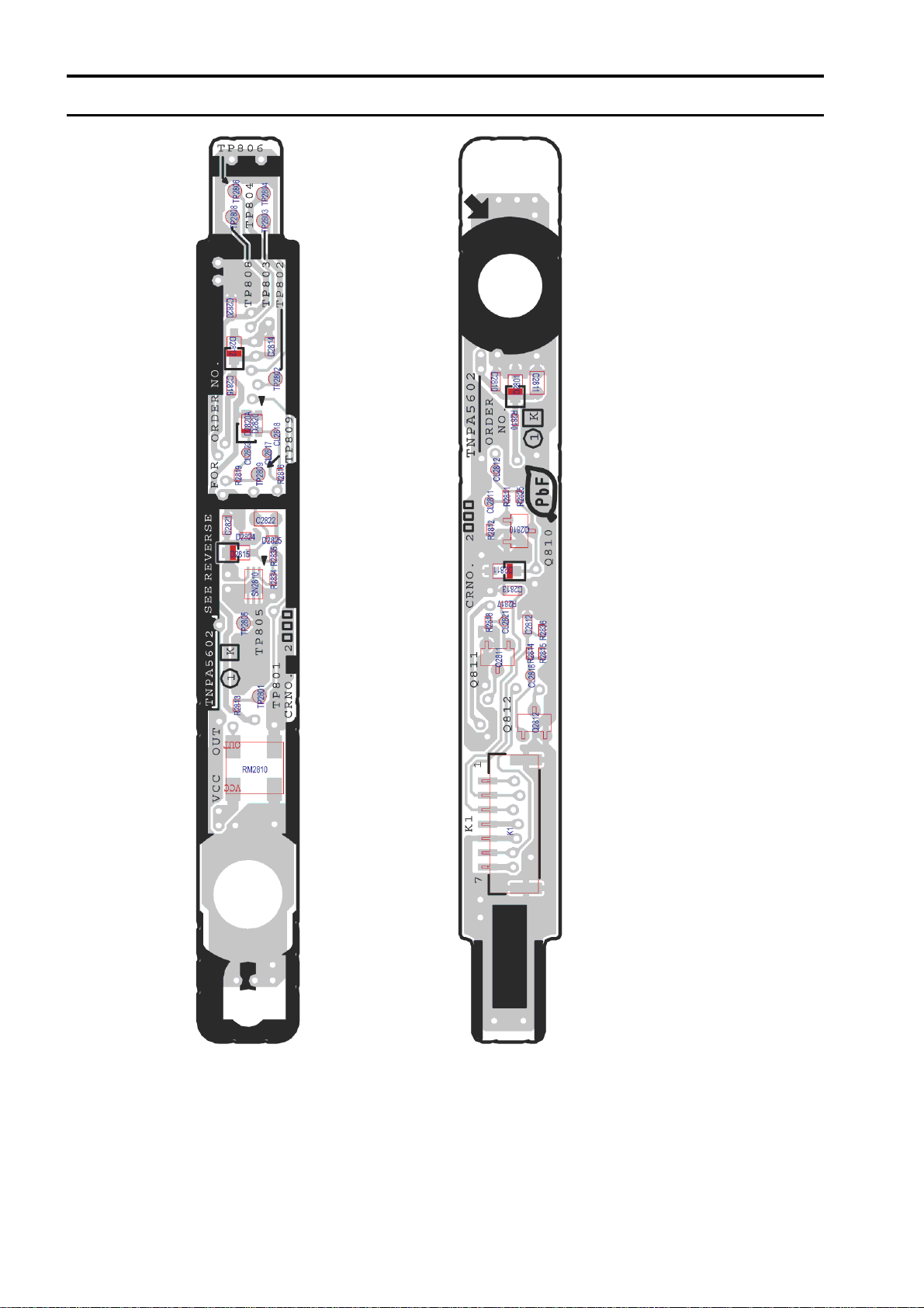
Model No. : TH-P50ST50A/D/G/K/M/P/S/T/V/Z K-Board
S-36
Page 79
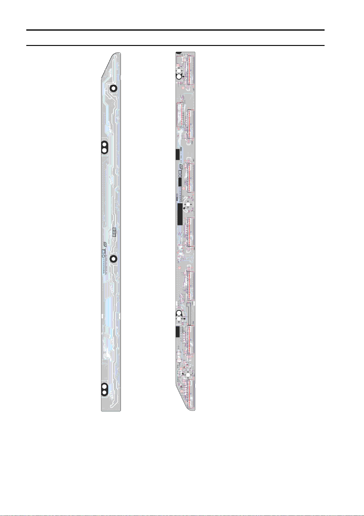
Model No. : TH-P50ST50A/D/G/K/M/P/S/T/V/Z C1-Board
S-37
Page 80
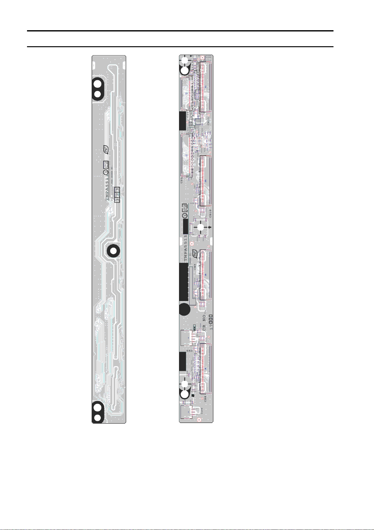
Model No. : TH-P50ST50A/D/G/K/M/P/S/T/V/Z C2-Board
S-38
Page 81
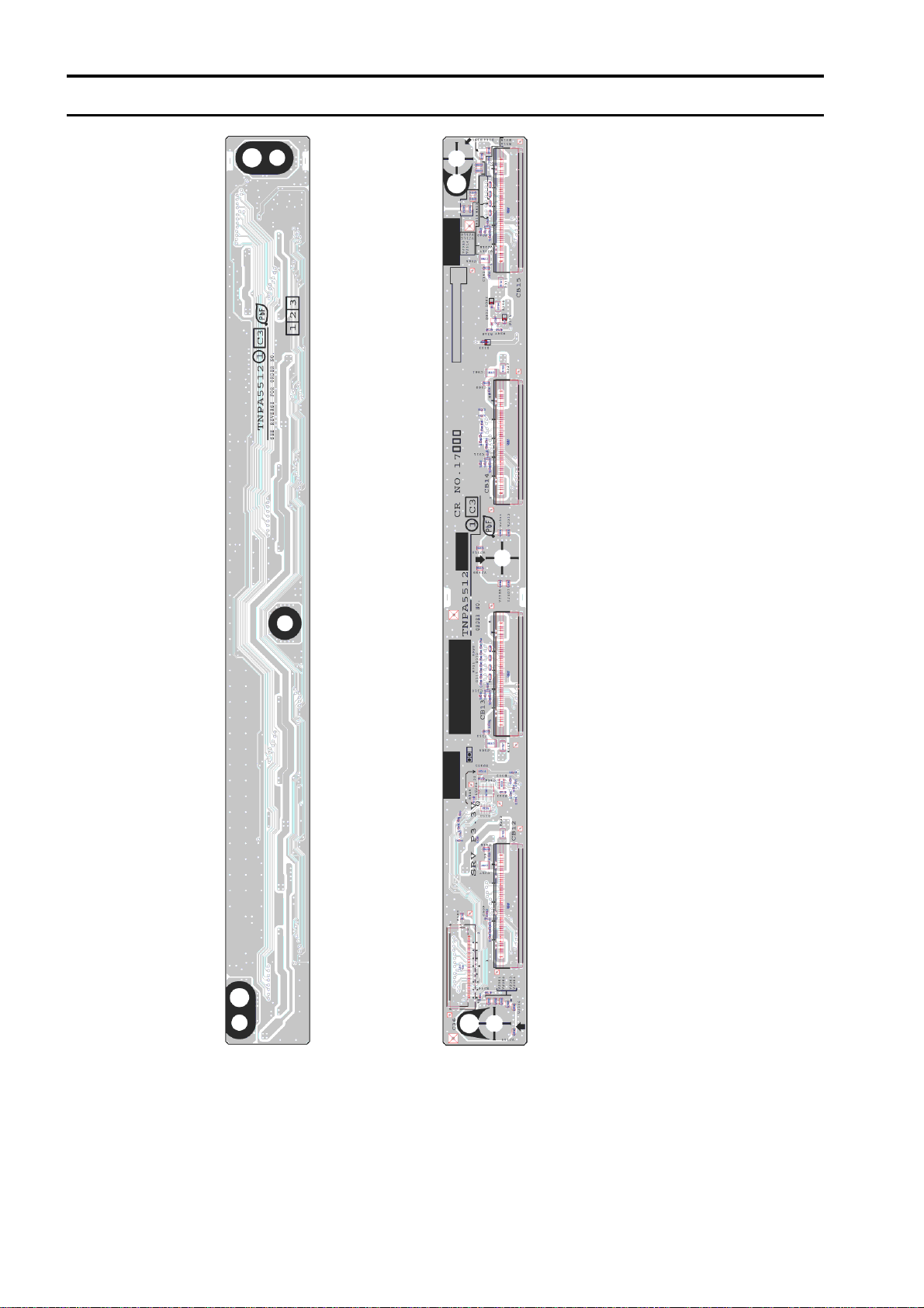
Model No. : TH-P50ST50A/D/G/K/M/P/S/T/V/Z C3-Board
S-39
Page 82
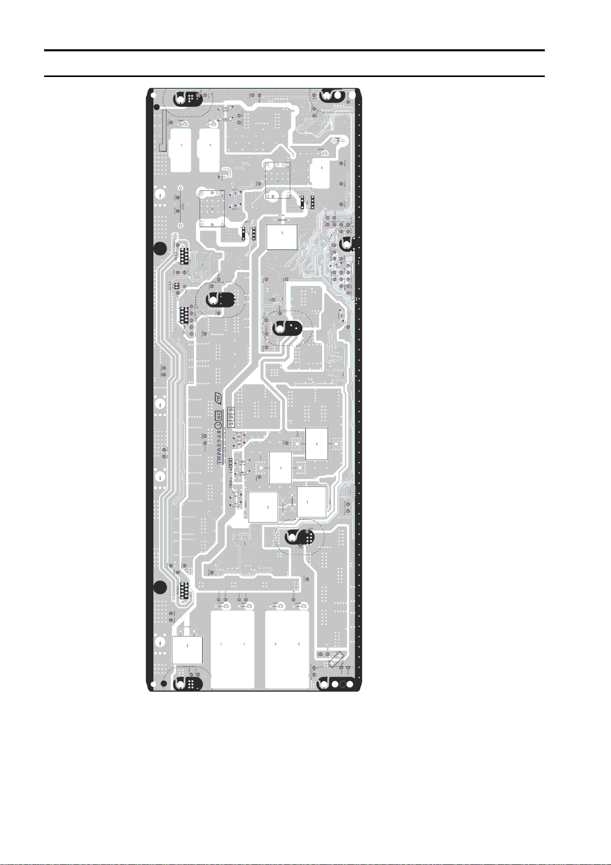
Model No. : TH-P50ST50A/D/G/K/M/P/S/T/V/Z SC-Board (Foil Side)
S-40
Page 83
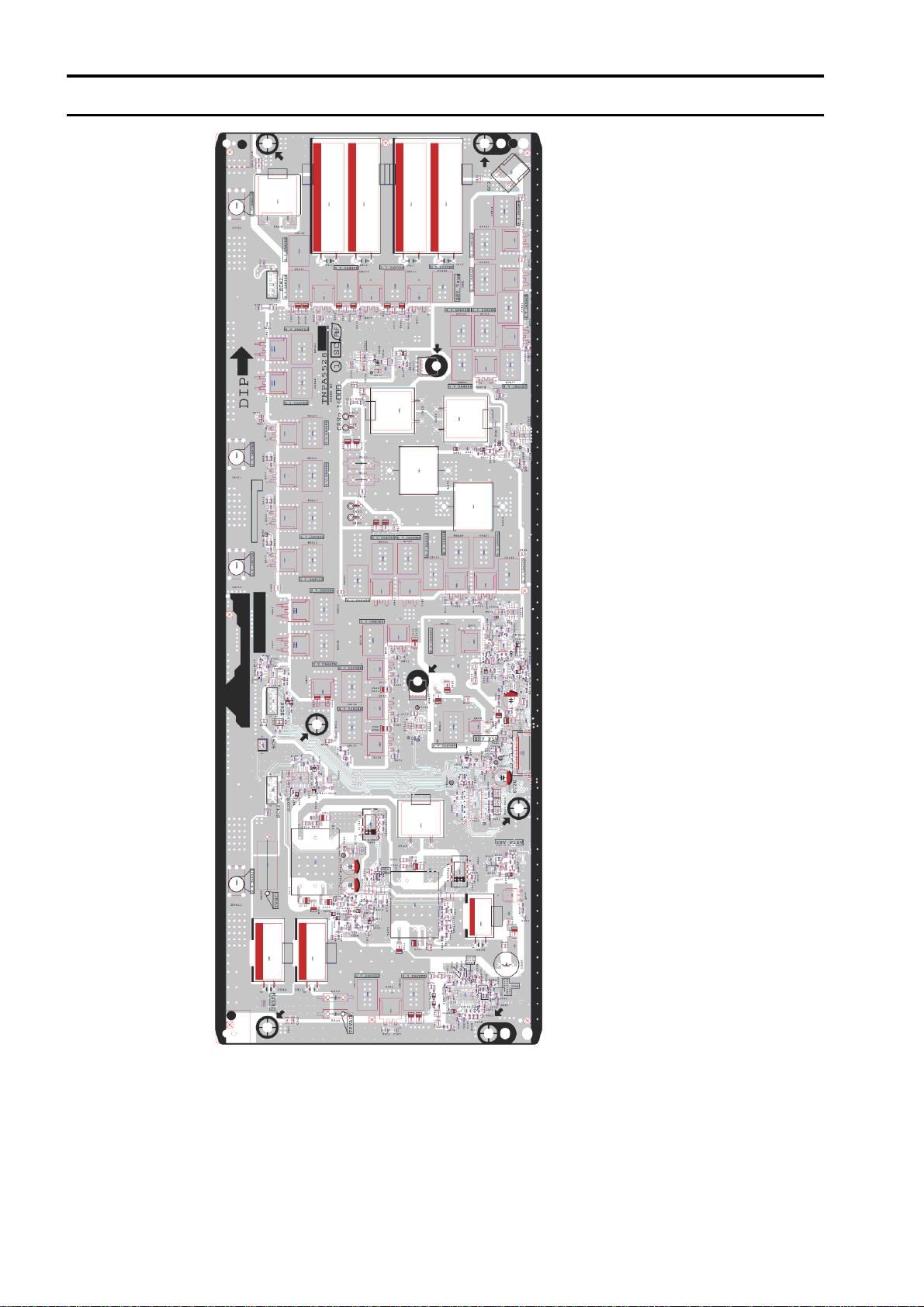
Model No. : TH-P50ST50A/D/G/K/M/P/S/T/V/Z SC-Board (Component Side)
S-41
Page 84
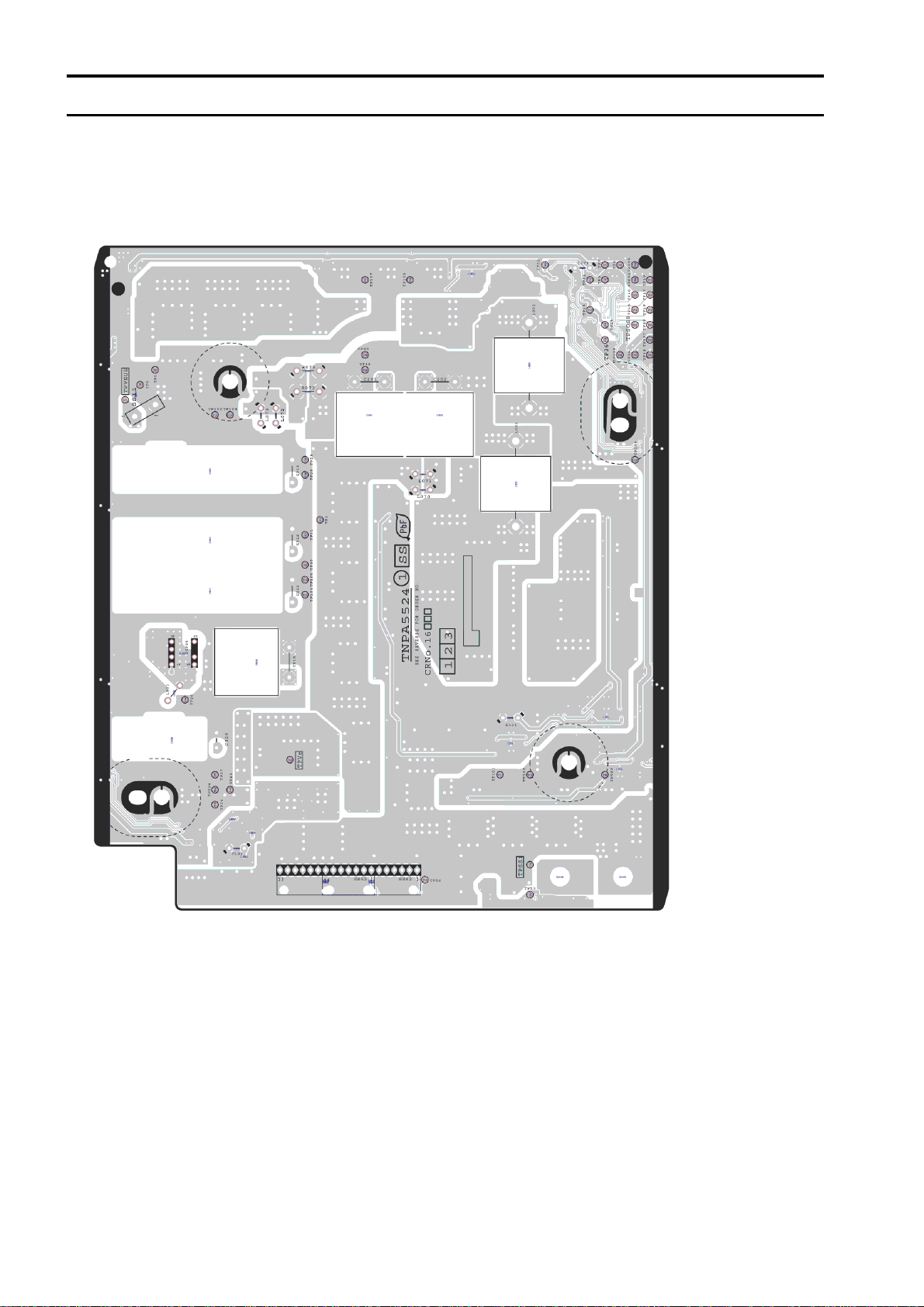
Model No. : TH-P50ST50A/D/G/K/M/P/S/T/V/Z SS-Board (Foil Side)
S-42
Page 85
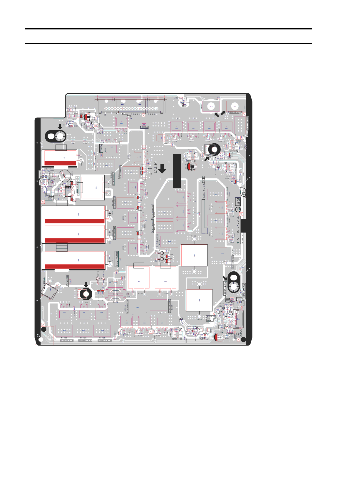
Model No. : TH-P50ST50A/D/G/K/M/P/S/T/V/Z SS-Board (Component Side)
S-43
Page 86
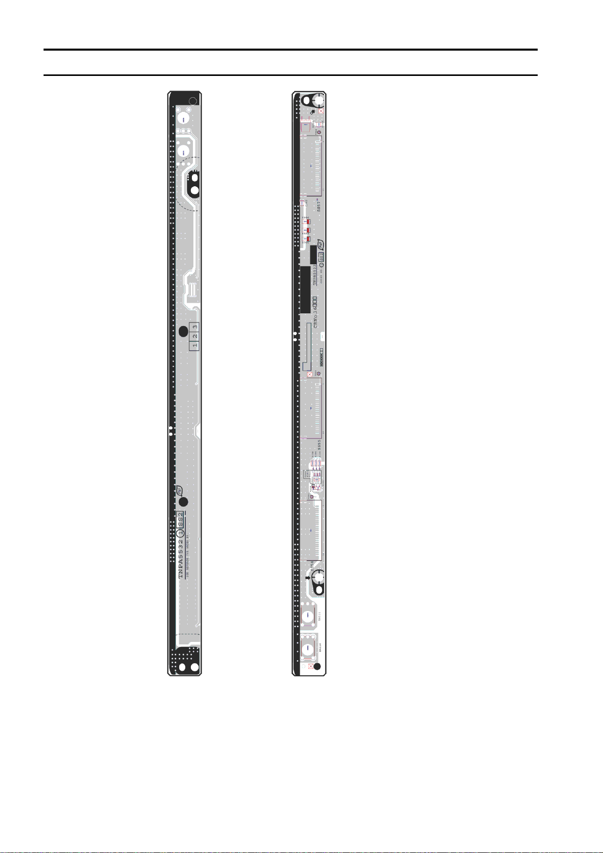
Model No. : TH-P50ST50A/D/G/K/M/P/S/T/V/Z SS2-Board
S-44
Page 87
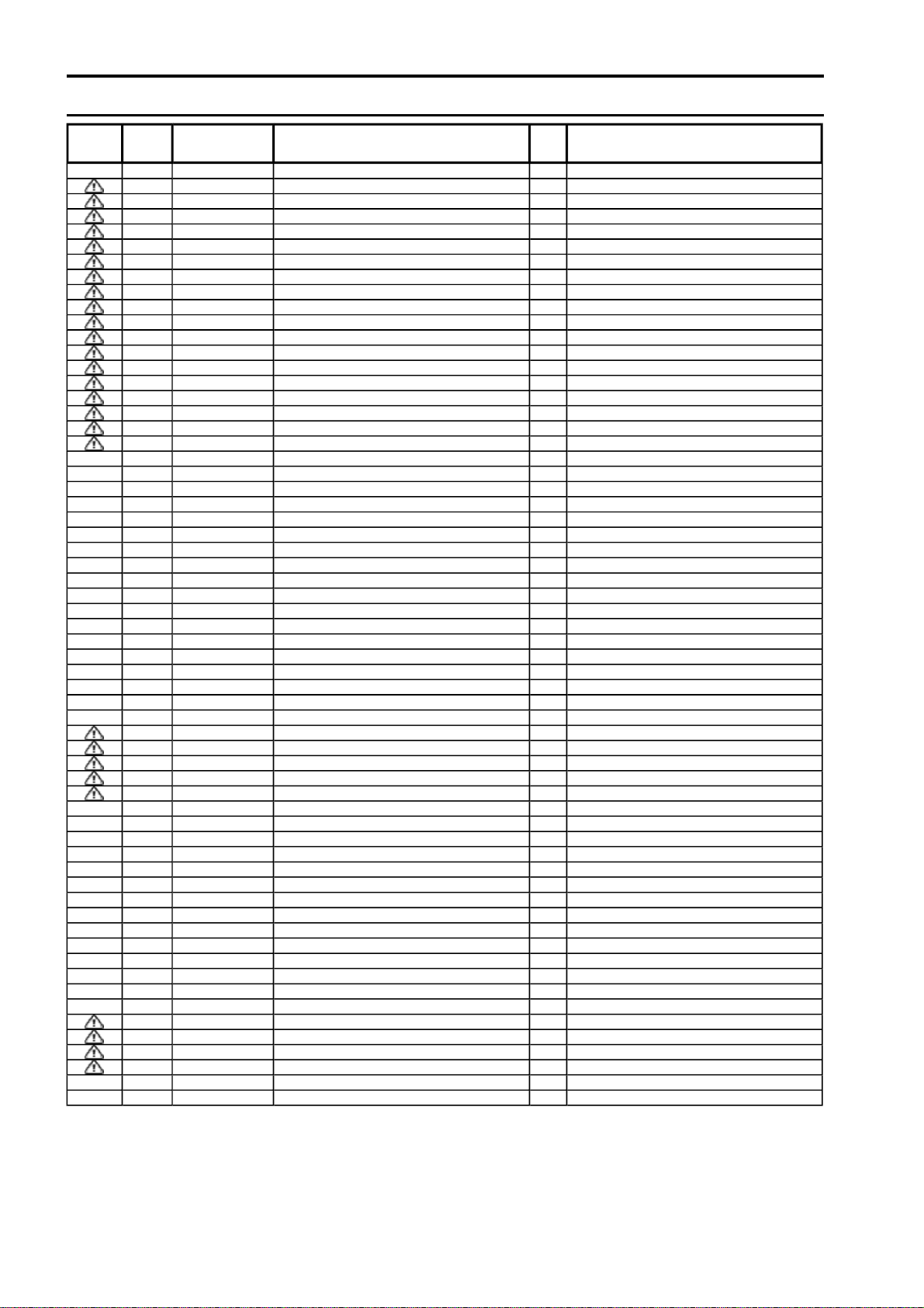
Model No. : TH-P50ST50A/D/G/K/M/P/S/T/V/Z Parts List
S-45
Safety
Ref.
No.
PCB TZTNP01PHUA A-PRINT COMPLETE 1 (A) (RTL)PAVCTH
PCB TZTNP01PCUD A-PRINT COMPLETE 1 (D) (RTL)PAVCTH
PCB TZTNP01PGUG A-PRINT COMPLETE 1 (G) (V) (RTL)PAVCTH
PCB TZTNP01NLUK A-PRINT COMPLETE 1 (K) (RTL)PAVCTH
PCB TZTNP01NHUM A-PRINT COMPLETE 1 (M) (T) (RTL)PAVCTH
PCB TZTNP01NXUP A-PRINT COMPLETE 1 (P) (RTL)PAVCTH
PCB TZTNP01PBUS A-PRINT COMPLETE 1 (S) (RTL)PAVCTH
PCB TZTNP01PAUZ A-PRINT COMPLETE 1 (Z) (RTL)PAVCTH
PCB TXNC11RFUU C1-PRINT COMPLETE 1 (RTL)PAVCTH
PCB TXNC21RFUU C2-PRINT COMPLETE 1 (RTL)PAVCTH
PCB TXNC31RFUU C3-PRINT COMPLETE 1 (RTL)PAVCTH
PCB TZRNP1STUE50 P-PRINT COMPLETE 1 (RTL)PAVCTH
PCB TXNSC1RFUU SC-PRINT COMPLETE 1 (RTL)PAVCTH
PCB TXNSD1RFUU SD-PRINT COMPLETE 1 PAVCTH
PCB TXNSS1RFUU SS-PRINT COMPLETE 1 (RTL)PAVCTH
PCB TXNSS21RFUU SS2-PRINT COMPLETE 1 (RTL)PAVCTH
PCB TXNSU1RFUU SU-PRINT COMPLETE 1 PAVCTH
PCB TXN/K1SUUE K-PRINT COMPLETE 1 (RTL)PAVCTH
A1 K1KA08B00270 8P CONNECTOR 1
A6 K1KY16BA0394 16P CONNECTOR 1 PAVCTH
A12 K1KY06BA0387 6P CONNECTOR 1 PAVCTH
A20 K1MY30BA0345 30P CONNECTOR 1
A31 K1MY55BA0345 55P CONNECTOR 1
A32 K1MY55BA0345 55P CONNECTOR 1
A33 K1MN20BA0231 20P CONNECTOR 1
A50 K1KY05AA0719 5P CONNECTOR 1
C10 K1KY03BA0387 3P CONNECTOR 1 PAVCTH
C11 K1MY55BA0345 55P CONNECTOR 1
C14 K1KY03AA0719 3P CONNECTOR 1
C20 K1KY03BA0387 3P CONNECTOR 1 PAVCTH
C21 K1MY55BA0345 55P CONNECTOR 1
C25 K1KY04BA0387 4P CONNECTOR 1 PAVCTH
C26 K1MY40BA0345 40P CONNECTOR 1
C36 K1MY40BA0345 40P CONNECTOR 1
C100 F0CAF334A105 C 0.33UF, 250V 1 PAVCTH
C101 F0CAF334A105 C 0.33UF, 250V 1 PAVCTH
C102 F1BAF471A088 C 470PF, 250V 1 PAVCTH
C103 F1BAF471A088 C 470PF, 250V 1 PAVCTH
C104 ECWF2W105KAC C 1UF, 450V 1 PAVCTH
C105 F1J1E334A272 C 0.33UF, 25V 1 PAVCTH
C106 F1J1E105A287 C 1UF, 25V 1 PAVCTH
C107 ECKD3A102KBP C 1000PF, 1KV 1
C108 ECKD3A102KBP C 1000PF, 1KV 1
C109 F1H1C105A179 C 1 uF 16 V 1 PAVCTH
C110 F1H1H104B047 C 0.1UF, 50V 1 PAVCTH
C111 F1H1H471B052 C 470PF, 50V 1 PAVCTH
C112 F1H1H104B047 C 0.1UF, 50V 1 PAVCTH
C113 F1J1E105A287 C 1UF, 25V 1 PAVCTH
C115 F1J1H102A909 C 1000pF, 50V 1 PAVCTH
C117 F1J1H102A909 C 1000pF, 50V 1 PAVCTH
C118 F1H1H104B047 C 0.1UF, 50V 1 PAVCTH
C120 F1J1H102A909 C 1000pF, 50V 1 PAVCTH
C123 F1H1H103B047 C 0.01UF, 50V 1 PAVCTH
C128 F2A2W101A248 E 100UF, 450V 1 PAVCTH
C129 F2A2W101A248 E 100UF, 450V 1 PAVCTH
C130 F2A2W101A248 E 100UF, 450V 1 PAVCTH
C143 ECWF2W105KAC C 1UF, 450V 1 PAVCTH
C145 F1J1E105A287 C 1UF, 25V 1 PAVCTH
C146 F1J1H103A900 C 0.01UF, 50V 1 PAVCTH
Part No. Part Name & Description Q'ty Remarks
Page 88
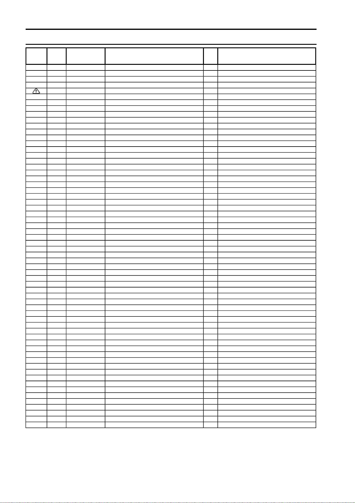
Model No. : TH-P50ST50A/D/G/K/M/P/S/T/V/Z Parts List
S-46
Safety
Ref.
No.
C200 F1H1H102B047 C 1000PF, 50V 1 PAVCTH
C201 F1J1E105A287 C 1UF, 25V 1 PAVCTH
C203 F1J1H222A911 C 2200pF, 50V 1 PAVCTH
C204 F2A1V470A092 C 47UF 35V 1
C206 F1BAF221A088 C 220PF, 250V 1 PAVCTH
C210 F1H1H103B047 C 0.01UF, 50V 1 PAVCTH
C211 F1H1H103B047 C 0.01UF, 50V 1 PAVCTH
C212 F1H1H103B047 C 0.01UF, 50V 1 PAVCTH
C213 F1H1H102B047 C 1000PF, 50V 1 PAVCTH
C214 F1H1E105A153 C 1UF, 16V 1 PAVCTH
C215 F2A1V470A092 C 47UF 35V 1
C216 F1H1H102B047 C 1000PF, 50V 1 PAVCTH
C217 F1H1H104B047 C 0.1UF, 50V 1 PAVCTH
C300 ECKD3A101KBP C 100PF, 1KV 1
C301 ECWH8333RHA C 0.033UF, 800V 1 PAVCTH
C302 ECWH8333RHA C 0.033UF, 800V 1 PAVCTH
C304 ECKD3A221KBP C 220PF, K, 1KV 1
C307 F1J1E105A287 C 1UF, 25V 1 PAVCTH
C308 F1J1H102A909 C 1000pF, 50V 1 PAVCTH
C309 F1J1H103A900 C 0.01UF, 50V 1 PAVCTH
C312 F1J1E105A287 C 1UF, 25V 1 PAVCTH
C313 F1H1H103B047 C 0.01UF, 50V 1 PAVCTH
C403 F1H1H103B047 C 0.01UF, 50V 1 PAVCTH
C404 F1H1H103B047 C 0.01UF, 50V 1 PAVCTH
C405 F1H1H103B047 C 0.01UF, 50V 1 PAVCTH
C407 F1H1H103B047 C 0.01UF, 50V 1 PAVCTH
C411 F1H1H104B047 C 0.1UF, 50V 1 PAVCTH
C412 F1H1H104B047 C 0.1UF, 50V 1 PAVCTH
C415 F1H1H102B047 C 1000PF, 50V 1 PAVCTH
C416 F1H1H104B047 C 0.1UF, 50V 1 PAVCTH
C417 F1J1H102A909 C 1000pF, 50V 1 PAVCTH
C419 F1J1H102A909 C 1000pF, 50V 1 PAVCTH
C420 F1J1E105A287 C 1UF, 25V 1 PAVCTH
C421 F1J1E105A287 C 1UF, 25V 1 PAVCTH
C426 F1H1H104B047 C 0.1UF, 50V 1 PAVCTH
C427 F1J1E105A287 C 1UF, 25V 1 PAVCTH
C502 F1J1H104A902 C 0.1UF, 50V 1 PAVCTH
C503 F2A1E471B730 E 470UF, 25V 1 PAVCTH
C504 F2A1E471B730 E 470UF, 25V 1 PAVCTH
C505 F2A1E471B730 E 470UF, 25V 1 PAVCTH
C506 F1J2E1020002 C 1000PF, 250V 1 PAVCTH
C507 F1H1H104B047 C 0.1UF, 50V 1 PAVCTH
C509 F1H1H104B047 C 0.1UF, 50V 1 PAVCTH
C510 F1H1H104B047 C 0.1UF, 50V 1 PAVCTH
C511 F1H1H104B047 C 0.1UF, 50V 1 PAVCTH
C512 F1J1H102A909 C 1000pF, 50V 1 PAVCTH
C513 F1J1H102A909 C 1000pF, 50V 1 PAVCTH
C518 F1J1E105A287 C 1UF, 25V 1 PAVCTH
C519 F1J1E105A287 C 1UF, 25V 1 PAVCTH
C520 F2A1E471B730 E 470UF, 25V 1 PAVCTH
C525 F1J1H102A909 C 1000pF, 50V 1 PAVCTH
C526 F1H1H104B047 C 0.1UF, 50V 1 PAVCTH
C527 F1J1H104A902 C 0.1UF, 50V 1 PAVCTH
C528 F1J1H104A902 C 0.1UF, 50V 1 PAVCTH
C529 F1H1H104B047 C 0.1UF, 50V 1 PAVCTH
C530 F1H1H104B047 C 0.1UF, 50V 1 PAVCTH
C531 F1H1H104B047 C 0.1UF, 50V 1 PAVCTH
C532 F1H1H104B047 C 0.1UF, 50V 1 PAVCTH
C533 F1H1H104B047 C 0.1UF, 50V 1 PAVCTH
C534 F1H1H104B047 C 0.1UF, 50V 1 PAVCTH
C601 F1H1H391B052 C 390PF, 50V 1 PAVCTH
C602 F1H1H104B047 C 0.1UF, 50V 1 PAVCTH
Part No. Part Name & Description Q'ty Remarks
Page 89
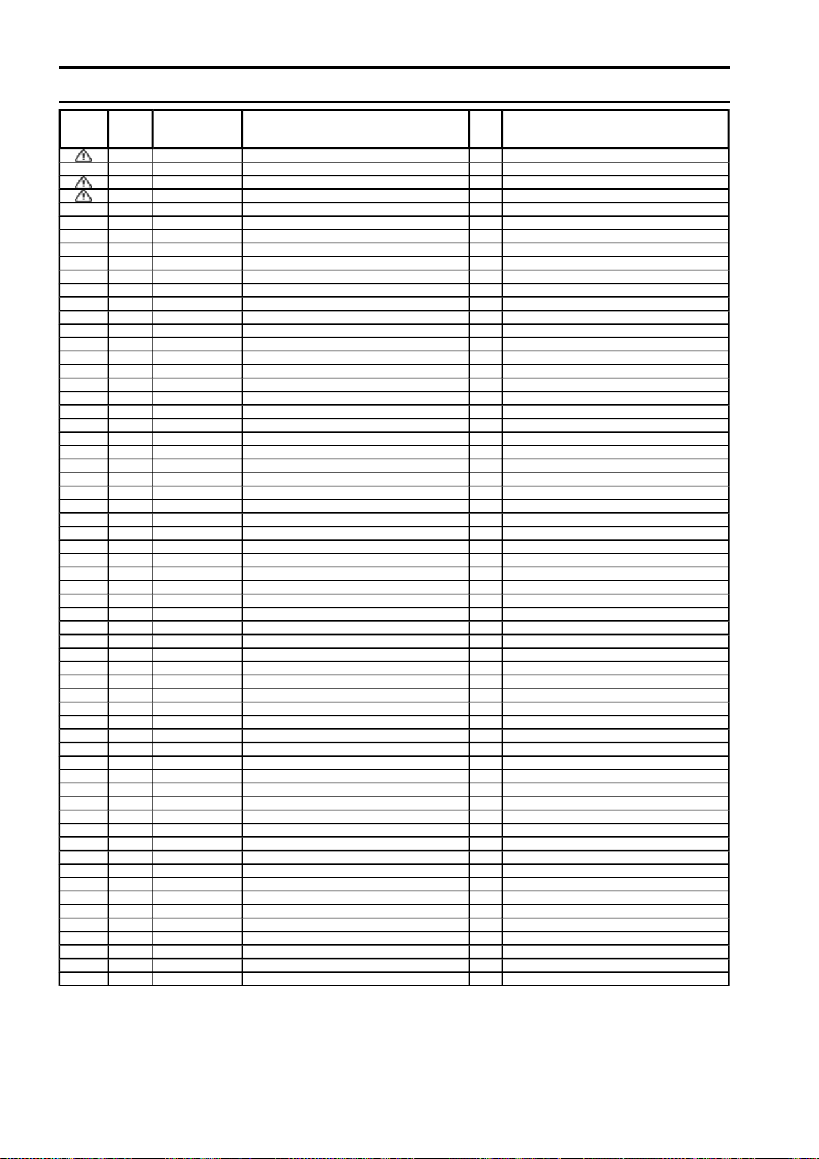
Model No. : TH-P50ST50A/D/G/K/M/P/S/T/V/Z Parts List
S-47
Safety
Ref.
No.
C603 F2AZZ821A034 E 820UF, 80V 1 PAVCTH
C604 F2A1J1520008 E 1500UF, 63V 1 PAVCTH
C700 F2A2E181A292 E 180UF, 250V 1 PAVCTH
C701 F2A2E181A292 E 180UF, 250V 1 PAVCTH
C703 F1J1E334A272 C 0.33UF, 25V 1 PAVCTH
C705 F1J1E105A287 C 1UF, 25V 1 PAVCTH
C707 F1H1H102B047 C 1000PF, 50V 1 PAVCTH
C2000 F1G1E1030005 C 0.01UF 25V 1
C2001 F1J1A106A110 C 10UF, 10V 1 PAVCTH
C2002 F1J1E105A287 C 1UF, 25V 1 PAVCTH
C2003 F1J1E105A287 C 1UF, 25V 1 PAVCTH
C2006 F1G1C104A077 C 0.1UF 16V 1
C2007 F1G1A105A047 C 1UF 10V 1
C2008 F1G1A105A047 C 1UF 10V 1
C2009 F1G1E1030005 C 0.01UF 25V 1
C2010 F1G1A105A047 C 1UF 10V 1
C2013 F1G1E1030005 C 0.01UF 25V 1
C2014 F1G1E1030005 C 0.01UF 25V 1
C2018 F1G1H1020008 C 1000PF 50V 1
C2019 F1G1E1030005 C 0.01UF 25V 1
C2026 F1G1C104A077 C 0.1UF 16V 1
C2032 F1H0J4750004 C 4.7UF, 16V 1
C2035 F1J1A106A087 C 10UF, 10V 1
C2036 F1J1A106A087 C 10UF, 10V 1
C2810 F1H1H103B047 C 0.01UF, 50V 1 PAVCTH
C2811 F1J1A106A087 C 10UF, 10V 1
C2815 F1H1H103B047 C 0.01UF, 50V 1 PAVCTH
C2821 ECJ1XB1C104K C 0.1UF, Z, 16V 1
C3040 F1J1A106A110 C 10UF, 10V 1 PAVCTH
C3042 F1J1A106A110 C 10UF, 10V 1 PAVCTH
C3045 F1J1A106A110 C 10UF, 10V 1 PAVCTH
C3046 F1G1A105A047 C 1UF 10V 1
C3047 F1G1A105A047 C 1UF 10V 1
C3050 F1K1E106A134 C 10UF, 25V 1
C3057 F1G1A105A047 C 1UF 10V 1
C3058 F1G1A105A047 C 1UF 10V 1
C3084 F1G1A105A047 C 1UF 10V 1
C3085 F1G1A105A047 C 1UF 10V 1
C3086 F1G1A105A047 C 1UF 10V 1
C3105 F1G1H471A834 C 470PF, 50V 1 PAVCTH
C3106 F1G1H471A834 C 470PF, 50V 1 PAVCTH
C3108 F1G1E333A059 C 0.033UF, 25V 1 PAVCTH
C3109 F1G1E333A059 C 0.033UF, 25V 1 PAVCTH
C3137 F1G1H471A834 C 470PF, 50V 1 PAVCTH
C3138 F1G1H471A834 C 470PF, 50V 1 PAVCTH
C3141 F1G1H471A834 C 470PF, 50V 1 PAVCTH
C3142 F1G1H471A834 C 470PF, 50V 1 PAVCTH
C3151 F1G1A105A047 C 1UF 10V 1
C3152 F1G1A105A047 C 1UF 10V 1
C3182 F1G1A105A047 C 1UF 10V 1
C3183 F1G1A105A047 C 1UF 10V 1
C3184 F1G1A105A047 C 1UF 10V 1
C3186 F1G1A105A047 C 1UF 10V 1
C3202 F1G1C104A077 C 0.1UF 16V 1
C3305 F2H1A101A040 C 100UF, 10V 1
C3307 F2H1A101A040 C 100UF, 10V 1
C4799 F1G1A105A047 C 1UF 10V 1
C4900 F1K1V106A010 C 10UF, 25V 1 PAVCTH
C4901 F1K1V106A010 C 10UF, 25V 1 PAVCTH
C4902 F1G1H1020008 C 1000PF 50V 1
C4903 F1G1C104A077 C 0.1UF 16V 1
C4904 F1G1C104A077 C 0.1UF 16V 1
Part No. Part Name & Description Q'ty Remarks
Page 90
Model No. : TH-P50ST50A/D/G/K/M/P/S/T/V/Z Parts List
S-48
Safety
Ref.
No.
C4905 F1G1C104A077 C 0.1UF 16V 1
C4906 F1G1C104A077 C 0.1UF 16V 1
C4907 F1K1V106A010 C 10UF, 25V 1 PAVCTH
C4908 F1G1H1020008 C 1000PF 50V 1
C4909 F1K1V106A010 C 10UF, 25V 1 PAVCTH
C4921 F1J1E105A287 C 1UF, 25V 1 PAVCTH
C4922 F1J1E105A287 C 1UF, 25V 1 PAVCTH
C4923 F1J1E105A287 C 1UF, 25V 1 PAVCTH
C4924 F1J1E105A287 C 1UF, 25V 1 PAVCTH
C4931 F1K1V106A010 C 10UF, 25V 1 PAVCTH
C4932 F1G1H1020008 C 1000PF 50V 1
C4933 F1G1C104A077 C 0.1UF 16V 1
C4934 F1G1C104A077 C 0.1UF 16V 1
C4935 F1G1C104A077 C 0.1UF 16V 1
C4936 F1G1C104A077 C 0.1UF 16V 1
C4937 F1K1V106A010 C 10UF, 25V 1 PAVCTH
C4946 F1J1E474A272 C 0.47UF, 25V 1 PAVCTH
C4947 F1J1E474A272 C 0.47UF, 25V 1 PAVCTH
C5000 F1G1E1030005 C 0.01UF 25V 1
C5002 F1JZZ1060001 C 10UF, 20V 1 PAVCTH
C5003 F1H1C105A145 C 1 uF 16 V 1
C5007 F1G1C104A077 C 0.1UF 16V 1
C5009 F1G1C104A077 C 0.1UF 16V 1
C5011 F1G1C104A077 C 0.1UF 16V 1
C5012 EEEHB1C101UP C 100PF, J, 16V 1
C5013 F1G1A105A047 C 1UF 10V 1
C5014 F1G1A105A047 C 1UF 10V 1
C5015 F1G1A105A047 C 1UF 10V 1
C5016 F1G1A105A047 C 1UF 10V 1
C5017 F1G1A105A047 C 1UF 10V 1
C5018 F1G1C104A077 C 0.1UF 16V 1
C5020 F1G1E1030005 C 0.01UF 25V 1
C6704 F1J1A106A110 C 10UF, 10V 1 PAVCTH
C6707 F1G1C104A077 C 0.1UF 16V 1
C6708 F1J1A106A110 C 10UF, 10V 1 PAVCTH
C6710 F1G1C104A077 C 0.1UF 16V 1
C6719 F1G1H220A834 C 22PF, 50V 1 PAVCTH
C6720 F1G1H220A834 C 22PF, 50V 1 PAVCTH
C6721 F1G1H220A834 C 22PF, 50V 1 PAVCTH
C6722 F1G1E472A144 C 4700pF 25V 1 PAVCTH
C6723 F1G1H101A834 C 100PF 50V 1 PAVCTH
C6724 F1G1H101A834 C 100PF 50V 1 PAVCTH
C6725 F1G1H220A834 C 22PF, 50V 1 PAVCTH
C6726 F1G1H470A834 C 47PF, 50V 1 PAVCTH
C6727 F1G1H470A834 C 47PF, 50V 1 PAVCTH
C6733 F1G1C104A077 C 0.1UF 16V 1
C6734 F1G1C104A077 C 0.1UF 16V 1
C6735 F1G1C104A077 C 0.1UF 16V 1
C6740 F1G1C104A077 C 0.1UF 16V 1
C6741 F1G1C104A077 C 0.1UF 16V 1
C6742 F1G1C104A077 C 0.1UF 16V 1
C6743 F1G1C104A077 C 0.1UF 16V 1
C6744 F1G1C104A077 C 0.1UF 16V 1
C8002 F1J1A106A087 C 10UF, 10V 1
C8004 F1G1C104A077 C 0.1UF 16V 1
C8005 F1G1C104A077 C 0.1UF 16V 1
C8007 F1J1A106A087 C 10UF, 10V 1
C8014 F1J0G2260001 C 22 UF 4 V 1
C8017 F1G1C104A077 C 0.1UF 16V 1
C8019 F1G1C104A077 C 0.1UF 16V 1
C8020 F1G1C104A077 C 0.1UF 16V 1
C8022 F1G1C104A077 C 0.1UF 16V 1
Part No. Part Name & Description Q'ty Remarks
Page 91
Model No. : TH-P50ST50A/D/G/K/M/P/S/T/V/Z Parts List
S-49
Safety
Ref.
No.
C8023 F1G1C104A077 C 0.1UF 16V 1
C8024 F1G1C104A077 C 0.1UF 16V 1
C8025 F1G1A105A047 C 1UF 10V 1
C8031 F1J1A106A087 C 10UF, 10V 1
C8033 F1J1A106A087 C 10UF, 10V 1
C8034 F1J0G2260001 C 22 UF 4 V 1
C8035 F1G1C104A077 C 0.1UF 16V 1
C8036 F1G1A105A047 C 1UF 10V 1
C8038 F1J0G2260001 C 22 UF 4 V 1
C8039 F1J0G2260001 C 22 UF 4 V 1
C8100 F1G1C223A146 C 0.022UF, 16V 1 PAVCTH
C8101 F1H1C105A145 C 1 uF 16 V 1
C8102 F1G1C104A077 C 0.1UF 16V 1
C8103 F1K1E106A134 C 10UF, 25V 1
C8105 F1J0G2260001 C 22 UF 4 V 1
C8106 F1J0G2260001 C 22 UF 4 V 1
C8108 ECJ1VB1E104K C 0.1 UF, 25V 1
C8110 F1G1C223A146 C 0.022UF, 16V 1 PAVCTH
C8111 F1H1C105A145 C 1 uF 16 V 1
C8112 F1G1C104A077 C 0.1UF 16V 1
C8113 F1K1E106A134 C 10UF, 25V 1
C8115 F1J0G2260001 C 22 UF 4 V 1
C8116 F1J0G2260001 C 22 UF 4 V 1
C8118 ECJ1VB1E104K C 0.1 UF, 25V 1
C8203 F1G1C104A077 C 0.1UF 16V 1
C8204 F1G1C104A077 C 0.1UF 16V 1
C8205 F1G1C104A077 C 0.1UF 16V 1
C8206 F1G1C104A077 C 0.1UF 16V 1
C8207 F1J1A106A087 C 10UF, 10V 1
C8208 F1G1C104A077 C 0.1UF 16V 1
C8210 F1G1C104A077 C 0.1UF 16V 1
C8212 F1G1C104A077 C 0.1UF 16V 1
C8215 F1G1C104A077 C 0.1UF 16V 1
C8216 F1J1A106A087 C 10UF, 10V 1
C8218 F1G1C104A077 C 0.1UF 16V 1
C8220 F1G1C104A077 C 0.1UF 16V 1
C8221 F1G1C104A077 C 0.1UF 16V 1
C8224 F1G1C104A077 C 0.1UF 16V 1
C8229 F1G1A105A047 C 1UF 10V 1
C8230 F1G1C104A077 C 0.1UF 16V 1
C8231 F1G1C104A077 C 0.1UF 16V 1
C8232 F1G1C104A077 C 0.1UF 16V 1
C8300 F1G1H9R0A831 C 9 PF, 50V 1 PAVCTH
C8301 F1G1H9R0A831 C 9 PF, 50V 1 PAVCTH
C8304 F1G1A105A047 C 1UF 10V 1
C8305 F1G1A105A047 C 1UF 10V 1
C8306 F1G1A105A047 C 1UF 10V 1
C8307 F1G1A105A047 C 1UF 10V 1
C8308 F1G1A105A047 C 1UF 10V 1
C8309 F1G1A105A047 C 1UF 10V 1
C8310 F1G1A105A047 C 1UF 10V 1
C8311 F1G1A105A047 C 1UF 10V 1
C8312 F1G1A105A047 C 1UF 10V 1
C8602 F1G1H120A834 C 12PF, 50V 1 PAVCTH
C8603 F1G1H120A834 C 12PF, 50V 1 PAVCTH
C8604 F1G1C104A077 C 0.1UF 16V 1
C8605 F1G1C104A077 C 0.1UF 16V 1
C8607 F1G1C104A077 C 0.1UF 16V 1
C8608 F1G1C104A077 C 0.1UF 16V 1
C8609 F1H1C105A145 C 1 uF 16 V 1
C8610 F1H1C105A145 C 1 uF 16 V 1
C8611 F1G1C104A077 C 0.1UF 16V 1
Part No. Part Name & Description Q'ty Remarks
Page 92
Model No. : TH-P50ST50A/D/G/K/M/P/S/T/V/Z Parts List
S-50
Safety
Ref.
No.
C8613 F1J1A106A110 C 10UF, 10V 1 PAVCTH
C8615 F1G1C104A077 C 0.1UF 16V 1
C8616 F1G1C104A077 C 0.1UF 16V 1
C8617 F1G1C1030008 C 0.01UF 16V 1
C8619 F1G1C104A077 C 0.1UF 16V 1
C8620 F1G1C104A077 C 0.1UF 16V 1
C8627 F1G1C104A077 C 0.1UF 16V 1
C8628 F1K0J226A049 C 22UF, 6.3V 1
C8629 F1K0J226A049 C 22UF, 6.3V 1
C8630 EEEHB0J221UP E 220UF, 6.3V 1
C8631 EEEHB0J221UP E 220UF, 6.3V 1
C8632 F1J1A106A110 C 10UF, 10V 1 PAVCTH
C8633 F1G1C104A077 C 0.1UF 16V 1
C8637 F1J1A106A110 C 10UF, 10V 1 PAVCTH
C8638 F1G1C104A077 C 0.1UF 16V 1
C8639 F1J1A106A110 C 10UF, 10V 1 PAVCTH
C8640 F1G1C104A077 C 0.1UF 16V 1
C8642 F1J1A106A110 C 10UF, 10V 1 PAVCTH
C8643 F1G1C104A077 C 0.1UF 16V 1
C8644 F1G1C1030008 C 0.01UF 16V 1
C8645 F1G1C104A077 C 0.1UF 16V 1
C8646 F1G1C104A077 C 0.1UF 16V 1
C8647 EEEHB0J221UP E 220UF, 6.3V 1
C8648 F1G1C104A077 C 0.1UF 16V 1
C8649 F1G1C104A077 C 0.1UF 16V 1
C8652 F1G1C104A077 C 0.1UF 16V 1
C8653 F1G1H8R0A831 C 8 PF, 50V 1 PAVCTH
C8654 F1G1H8R0A831 C 8 PF, 50V 1 PAVCTH
C8655 F1G1C104A077 C 0.1UF 16V 1
C8658 F1J1A106A110 C 10UF, 10V 1 PAVCTH
C8659 F1G1C104A077 C 0.1UF 16V 1
C8674 F1G1C104A077 C 0.1UF 16V 1
C8675 F1G1C104A077 C 0.1UF 16V 1
C8676 F1G1C104A077 C 0.1UF 16V 1
C8721 F1K1E106A134 C 10UF, 25V 1
C8722 F1K1E106A134 C 10UF, 25V 1
C8723 ECJ1VB1E104K C 0.1 UF, 25V 1
C8724 F1J1A106A110 C 10UF, 10V 1 PAVCTH
C8725 F1J1A106A110 C 10UF, 10V 1 PAVCTH
C8728 F1H1C105A145 C 1 uF 16 V 1
C8729 F1G1E472A086 C 4700pF 25V 1
C8730 F1G1C104A077 C 0.1UF 16V 1
C8731 F1G1E1030005 C 0.01UF 25V 1
C8732 F1K1V106A010 C 10UF, 25V 1 PAVCTH
C8733 F1J1A106A110 C 10UF, 10V 1 PAVCTH
C8734 F1J1A106A110 C 10UF, 10V 1 PAVCTH
C8737 F1G1C104A077 C 0.1UF 16V 1
C8738 F1G1H222A830 C 2200PF, 50V 1 PAVCTH
C8739 F1G1E1030005 C 0.01UF 25V 1
C8747 F1G1A105A047 C 1UF 10V 1
C8748 F1H0J4750004 C 4.7UF, 16V 1
C8749 F1G1A105A047 C 1UF 10V 1
C8750 F1G1A105A047 C 1UF 10V 1
C8757 F1J1A106A110 C 10UF, 10V 1 PAVCTH
C8758 F1J1A106A110 C 10UF, 10V 1 PAVCTH
C8771 F1G1C104A077 C 0.1UF 16V 1
C8772 F1G1C104A077 C 0.1UF 16V 1
C8773 F1G1C104A077 C 0.1UF 16V 1
C8790 F1J1A106A110 C 10UF, 10V 1 PAVCTH
C8791 F1J1A106A110 C 10UF, 10V 1 PAVCTH
C8900 F1G1C104A077 C 0.1UF 16V 1
C8901 F1G1C104A077 C 0.1UF 16V 1
Part No. Part Name & Description Q'ty Remarks
Page 93
Model No. : TH-P50ST50A/D/G/K/M/P/S/T/V/Z Parts List
S-51
Safety
Ref.
No.
C8902 F1G1C104A077 C 0.1UF 16V 1
C0902 F1G1H101A834 C 100PF 50V 1 PAVCTH
C0903 F1G1H101A834 C 100PF 50V 1 PAVCTH
C9096 F1J1A106A110 C 10UF, 10V 1 PAVCTH
C9102 F1JZZ1060001 C 10UF, 20V 1 PAVCTH
C9103 F1G1E1030005 C 0.01UF 25V 1
C9107 F1G1C104A077 C 0.1UF 16V 1
C9111 F1K1E106A134 C 10UF, 25V 1
C9116 F1G1C104A077 C 0.1UF 16V 1
C9119 ECJ1VB1E104K C 0.1 UF, 25V 1
C9120 F1H1C105A145 C 1 uF 16 V 1
C9121 F1G1H1020008 C 1000PF 50V 1
C9122 F1G1A105A047 C 1UF 10V 1
C9123 F1G1A105A047 C 1UF 10V 1
C9222 F1K1E106A134 C 10UF, 25V 1
C9235 ECJ1VB1E104K C 0.1 UF, 25V 1
C9237 F1K0J226A049 C 22UF, 6.3V 1
C9238 F1K0J226A049 C 22UF, 6.3V 1
C9300 F1G1C104A077 C 0.1UF 16V 1
C9301 F1G1H180A834 C 18PF, 50V 1 PAVCTH
C9302 F1G1H180A834 C 18PF, 50V 1 PAVCTH
C9308 F1G1C104A077 C 0.1UF 16V 1
C9309 F1G1A105A047 C 1UF 10V 1
C9311 F1G1C104A077 C 0.1UF 16V 1
C9312 F1J1A106A110 C 10UF, 10V 1 PAVCTH
C9317 F1G1A105A047 C 1UF 10V 1
C9318 F1G1A105A047 C 1UF 10V 1
C9319 F1G1A105A047 C 1UF 10V 1
C9320 F1G1A105A047 C 1UF 10V 1
C9321 F1G1A105A047 C 1UF 10V 1
C9322 F1G1A105A047 C 1UF 10V 1
C9323 F1G1A105A047 C 1UF 10V 1
C9324 F1G1A105A047 C 1UF 10V 1
C9325 F1G1A105A047 C 1UF 10V 1
C9326 F1G1A105A047 C 1UF 10V 1
C9335 F1J1A106A110 C 10UF, 10V 1 PAVCTH
C9336 F1J1A106A110 C 10UF, 10V 1 PAVCTH
C9337 F1J1A106A110 C 10UF, 10V 1 PAVCTH
C9346 F1G1A105A047 C 1UF 10V 1
C9347 F1G1A105A047 C 1UF 10V 1
C9354 F1G1A105A047 C 1UF 10V 1
C9355 F1J1A106A110 C 10UF, 10V 1 PAVCTH
C9356 F1J1A106A110 C 10UF, 10V 1 PAVCTH
C9357 F1J1A106A110 C 10UF, 10V 1 PAVCTH
C9366 F1G1A105A047 C 1UF 10V 1
C9367 F1G1A105A047 C 1UF 10V 1
C9368 F1G1A105A047 C 1UF 10V 1
C9371 F1J1A106A110 C 10UF, 10V 1 PAVCTH
C9375 F1G1C104A077 C 0.1UF 16V 1
C9376 F1G1A105A047 C 1UF 10V 1
C9378 F1G1C104A077 C 0.1UF 16V 1
C9379 F1G1C104A077 C 0.1UF 16V 1
C9380 F1G1C104A077 C 0.1UF 16V 1
C9381 F1G1C104A077 C 0.1UF 16V 1
C9382 F1G1C104A077 C 0.1UF 16V 1
C9383 F1G1C104A077 C 0.1UF 16V 1
C9384 F1G1C104A077 C 0.1UF 16V 1
C9385 F1G1C104A077 C 0.1UF 16V 1
C9386 F1G1A105A047 C 1UF 10V 1
C9387 F1G1A105A047 C 1UF 10V 1
C9388 F1G1A105A047 C 1UF 10V 1
C9391 F1J1A106A110 C 10UF, 10V 1 PAVCTH
Part No. Part Name & Description Q'ty Remarks
Page 94
Model No. : TH-P50ST50A/D/G/K/M/P/S/T/V/Z Parts List
S-52
Safety
Ref.
No.
C9392 F1J1A106A110 C 10UF, 10V 1 PAVCTH
C9393 F1J1A106A110 C 10UF, 10V 1 PAVCTH
C9395 F1G1C104A077 C 0.1UF 16V 1
C9396 F1G1C104A077 C 0.1UF 16V 1
C9401 F1G1C104A077 C 0.1UF 16V 1
C9402 F1G1A105A047 C 1UF 10V 1
C9404 F1G1C104A077 C 0.1UF 16V 1
C9408 F1J1A106A110 C 10UF, 10V 1 PAVCTH
C9409 F1J1A106A110 C 10UF, 10V 1 PAVCTH
C9410 F1G1A105A047 C 1UF 10V 1
C9411 F1J1A106A110 C 10UF, 10V 1 PAVCTH
C9412 F1G1A105A047 C 1UF 10V 1
C9413 F1J1A106A110 C 10UF, 10V 1 PAVCTH
C9415 F1J1A106A110 C 10UF, 10V 1 PAVCTH
C9416 F1G1C104A077 C 0.1UF 16V 1
C9417 F1J1A106A110 C 10UF, 10V 1 PAVCTH
C9418 F1G1C104A077 C 0.1UF 16V 1
C9419 F1J1A106A110 C 10UF, 10V 1 PAVCTH
C9420 F1G1C104A077 C 0.1UF 16V 1
C9421 F1G1C104A077 C 0.1UF 16V 1
C9422 F1G1C104A077 C 0.1UF 16V 1
C9423 F1G1C104A077 C 0.1UF 16V 1
C9427 F1J1A106A110 C 10UF, 10V 1 PAVCTH
C9428 F1J1A106A110 C 10UF, 10V 1 PAVCTH
C9591 F1G1C104A077 C 0.1UF 16V 1
C9817 F1J1A106A110 C 10UF, 10V 1 PAVCTH
C9822 F1J1A106A110 C 10UF, 10V 1 PAVCTH
C9824 F1G1A105A047 C 1UF 10V 1
C9825 F1J1A106A110 C 10UF, 10V 1 PAVCTH
C9826 F1G1C104A077 C 0.1UF 16V 1
C16003 F1L2J562A021 C 5600PF, 630V 1 PAVCTH
C16011 F2A2E261A290 E 260UF, 250V 1 PAVCTH
C16012 F2A2E261A290 E 260UF, 250V 1 PAVCTH
C16018 F0C2E225A307 C 2.2UF, 250V 1 PAVCTH
C16024 F1K2J332A024 C 3300PF, 630V 1 PAVCTH
C16028 F1K2J222A024 C 2200PF, 630V 1 PAVCTH
C16041 ECJ1VB1H392K C 3900UF, 50V 1
C16044 F1K2J821A043 C 820PF, 630V 1 PAVCTH
C16051 ECJ1VB1H392K C 3900UF, 50V 1
C16053 ECJ1VB1H392K C 3900UF, 50V 1
C16061 F1K2J821A043 C 820PF, 630V 1 PAVCTH
C16074 F1L2J472A021 C 4700PF, 630V 1 PAVCTH
C16104 F1H1E470A130 C 47PF, 25V 1
C16105 F1H1E470A130 C 47PF, 25V 1
C16131 F1K1E105A029 C 1UF, 25V 1
C16132 F1H1C105A145 C 1 uF 16 V 1
C16133 F2A1E1010130 E 100UF, 25V 1
C16135 F1K1E105A029 C 1UF, 25V 1
C16153 F1K1E105A029 C 1UF, 25V 1
C16154 F1K1E105A029 C 1UF, 25V 1
C16191 F1K1E475A134 C 4.7UF 25V 1
C16192 ECJ1VB1E104K C 0.1 UF, 25V 1
C16193 F2A1E4700094 E 47UF, 25V 1
C16195 F1K1E105A029 C 1UF, 25V 1
C16201 F0C2E225A307 C 2.2UF, 250V 1 PAVCTH
C16202 F0C2E225A307 C 2.2UF, 250V 1 PAVCTH
C16242 F1H1C105A145 C 1 uF 16 V 1
C16243 ECJ1VB1H103K C 0.01UF, 50V 1
C16244 F1J1A106A087 C 10UF, 10V 1
C16271 F2A1E151B705 E 150UF, 25V 1
C16280 F1K1E105A029 C 1UF, 25V 1
C16281 ECJ1VB1E104K C 0.1 UF, 25V 1
Part No. Part Name & Description Q'ty Remarks
Page 95
Model No. : TH-P50ST50A/D/G/K/M/P/S/T/V/Z Parts List
S-53
Safety
Ref.
No.
C16284 F1H1H104A913 C 0.1UF, K , 50V 1
C16295 F1H1H104A913 C 0.1UF, K , 50V 1
C16315 ECJ1VB1A105K C 1UF, 10V 1
C16316 ECJ1XB1C104K C 0.1UF, Z, 16V 1
C16317 ECJ1VB1A105K C 1UF, 10V 1
C16318 F1J1H104A717 C 0.1UF, 50V 1
C16319 F1J1H104A717 C 0.1UF, 50V 1
C16328 F2A2T101A022 E 100UF, 220V 1 PAVCTH
C16351 F1H1H104A970 C 0.1UF, , 50V 1
C16352 F1H1H104A970 C 0.1UF, , 50V 1
C16353 F1H1H104A970 C 0.1UF, , 50V 1
C16361 F1L2J562A021 C 5600PF, 630V 1 PAVCTH
C16362 F1L2J562A021 C 5600PF, 630V 1 PAVCTH
C16401 F1L2J562A021 C 5600PF, 630V 1 PAVCTH
C16411 F2A2E261A290 E 260UF, 250V 1 PAVCTH
C16412 F2A2E261A290 E 260UF, 250V 1 PAVCTH
C16413 F2A2E261A290 E 260UF, 250V 1 PAVCTH
C16414 F0C2E155A307 C 1.5UF, 250V 1 PAVCTH
C16415 F0C2E105A307 C 1UF, 250V 1 PAVCTH
C16423 F1L2J562A021 C 5600PF, 630V 1 PAVCTH
C16441 ECJ1VB1H392K C 3900UF, 50V 1
C16442 ECJ1VB1H392K C 3900UF, 50V 1
C16450 F1L2J472A021 C 4700PF, 630V 1 PAVCTH
C16451 ECJ1VB1H392K C 3900UF, 50V 1
C16452 ECJ1VB1H392K C 3900UF, 50V 1
C16460 F1K2J222A024 C 2200PF, 630V 1 PAVCTH
C16502 F1K1E475A134 C 4.7UF 25V 1
C16503 F2A1E151B705 E 150UF, 25V 1
C16505 F1K1E105A029 C 1UF, 25V 1
C16506 F1H1C105A145 C 1 uF 16 V 1
C16508 F1K1E105A029 C 1UF, 25V 1
C16531 F1K1E475A134 C 4.7UF 25V 1
C16534 F1H1C105A145 C 1 uF 16 V 1
C16551 F1K1E105A029 C 1UF, 25V 1
C16561 F1J1A106A087 C 10UF, 10V 1
C16562 F1H1C105A145 C 1 uF 16 V 1
C16563 F1H1C105A145 C 1 uF 16 V 1
C16565 ECJ1VB1H103K C 0.01UF, 50V 1
C16566 ECJ1VB1H103K C 0.01UF, 50V 1
C16584 ECJ1VB1H392K C 3900UF, 50V 1
C16593 F1H1H102A831 C 1000PF, 50V 1 PAVCTH
C16602 F1H1H2200008 C 22PF, 50V 1
C16603 F1K2J471A042 C 470PF, 630V 1 PAVCTH
C16631 F0C2E225A307 C 2.2UF, 250V 1 PAVCTH
C16632 F0C2E225A307 C 2.2UF, 250V 1 PAVCTH
C16641 F1K2J222A024 C 2200PF, 630V 1 PAVCTH
C16661 F1K2J1020001 C 1000PF, 630V 1 PAVCTH
C16662 F1K2J1020001 C 1000PF, 630V 1 PAVCTH
C16663 F1K2J2210003 C 220PF, 630V 1 PAVCTH
C16668 F1H1H821A831 C 820 PF, 50V 1
C16685 F1H1H104A913 C 0.1UF, K , 50V 1
C16723 F1K1E105A029 C 1UF, 25V 1
C16724 F1K1E475A134 C 4.7UF 25V 1
C16753 F1K1E105A029 C 1UF, 25V 1
C16770 F1H1C105A145 C 1 uF 16 V 1
C16791 F2A1E151B705 E 150UF, 25V 1
C16793 F2A1E151B705 E 150UF, 25V 1
C16794 F1J1A106A087 C 10UF, 10V 1
C16795 F2A1E151B705 E 150UF, 25V 1
C16796 F1K1E475A134 C 4.7UF 25V 1
C16813 F2A2T101A022 E 100UF, 220V 1 PAVCTH
C16833 F1K2J1020001 C 1000PF, 630V 1 PAVCTH
Part No. Part Name & Description Q'ty Remarks
Page 96
Model No. : TH-P50ST50A/D/G/K/M/P/S/T/V/Z Parts List
S-54
Safety
Ref.
No.
C16834 F1K2J1020001 C 1000PF, 630V 1 PAVCTH
C16835 F2AZZ121A032 E 120UF, 80V 1 PAVCTH
C16842 F2A2C101A217 E 100UF, 160V 1 PAVCTH
C16843 ECJ1VB1A105K C 1UF, 10V 1
C16844 ECJ1XB1C104K C 0.1UF, Z, 16V 1
C16854 ECJ1XB1C104K C 0.1UF, Z, 16V 1
C16856 ECJ1VB1A105K C 1UF, 10V 1
C16858 ECJ1XB1C104K C 0.1UF, Z, 16V 1
C16860 ECJ1VB1A105K C 1UF, 10V 1
C16861 ECJ1XB1C104K C 0.1UF, Z, 16V 1
C16862 ECJ1VB1A105K C 1UF, 10V 1
C16863 ECJ1XB1C104K C 0.1UF, Z, 16V 1
C16891 F1K1E105A029 C 1UF, 25V 1
C16903 F1K2J222A024 C 2200PF, 630V 1 PAVCTH
C16907 F1K2J2210003 C 220PF, 630V 1 PAVCTH
C16908 F1L2J472A021 C 4700PF, 630V 1 PAVCTH
C16910 F1K2J821A043 C 820PF, 630V 1 PAVCTH
C16912 F1K2J821A043 C 820PF, 630V 1 PAVCTH
C17101 F1H1A105A099 C 1UF, 10V 1 PAVCTH
C17102 F1H1A105A099 C 1UF, 10V 1 PAVCTH
C17103 F1H1A105A099 C 1UF, 10V 1 PAVCTH
C17108 F1L2E224A028 C 0.22UF, 250V 1
C17109 F1L2E224A028 C 0.22UF, 250V 1
C17111 F1L2E224A028 C 0.22UF, 250V 1
C17131 F1H1A105A099 C 1UF, 10V 1 PAVCTH
C17132 F1H1A105A099 C 1UF, 10V 1 PAVCTH
C17134 F1L2E224A028 C 0.22UF, 250V 1
C17136 F1L2E224A028 C 0.22UF, 250V 1
C17137 F1H1A105A099 C 1UF, 10V 1 PAVCTH
C17138 F1H1A105A099 C 1UF, 10V 1 PAVCTH
C17139 F1L2E224A028 C 0.22UF, 250V 1
C17142 F1L2E224A028 C 0.22UF, 250V 1
C17143 ECJ1XB1C104K C 0.1UF, Z, 16V 1
C17154 F1H1H102A831 C 1000PF, 50V 1 PAVCTH
C17155 F1H1H102A831 C 1000PF, 50V 1 PAVCTH
C17156 F1H1H102A831 C 1000PF, 50V 1 PAVCTH
C17157 F1H1H102A831 C 1000PF, 50V 1 PAVCTH
C17201 F1H1A105A099 C 1UF, 10V 1 PAVCTH
C17204 F1H1A105A099 C 1UF, 10V 1 PAVCTH
C17207 F1H1A105A099 C 1UF, 10V 1 PAVCTH
C17208 F1H1A105A099 C 1UF, 10V 1 PAVCTH
C17209 ECJ1XB1C104K C 0.1UF, Z, 16V 1
C17249 F1L2E224A028 C 0.22UF, 250V 1
C17251 F1L2E224A028 C 0.22UF, 250V 1
C17253 F1L2E224A028 C 0.22UF, 250V 1
C17255 F1L2E224A028 C 0.22UF, 250V 1
C17309 F1H1A105A099 C 1UF, 10V 1 PAVCTH
C17310 F1H1A105A099 C 1UF, 10V 1 PAVCTH
C17311 F1H1A105A099 C 1UF, 10V 1 PAVCTH
C17312 F1H1A105A099 C 1UF, 10V 1 PAVCTH
C17357 F1L2E224A028 C 0.22UF, 250V 1
C17359 F1L2E224A028 C 0.22UF, 250V 1
C17361 F1L2E224A028 C 0.22UF, 250V 1
C17363 F1L2E224A028 C 0.22UF, 250V 1
C17364 ECJ1XB1C104K C 0.1UF, Z, 16V 1
CB1 K1MY55B00001 55P CONNECTOR 1
CB2 K1MY55B00001 55P CONNECTOR 1
CB3 K1MY55B00001 55P CONNECTOR 1
CB4 K1MY55B00001 55P CONNECTOR 1
CB5 K1MY55B00001 55P CONNECTOR 1
CB6 K1MY55B00001 55P CONNECTOR 1
Part No. Part Name & Description Q'ty Remarks
Page 97
Model No. : TH-P50ST50A/D/G/K/M/P/S/T/V/Z Parts List
S-55
Safety
Ref.
No.
CB7 K1MY55B00001 55P CONNECTOR 1
CB8 K1MY55B00001 55P CONNECTOR 1
CB9 K1MY55B00001 55P CONNECTOR 1
CB10 K1MY55B00001 55P CONNECTOR 1
CB11 K1MY55B00001 55P CONNECTOR 1
CB12 K1MY55B00001 55P CONNECTOR 1
CB13 K1MY55B00001 55P CONNECTOR 1
CB14 K1MY55B00001 55P CONNECTOR 1
CB15 K1MY55B00001 55P CONNECTOR 1
CN0100 K1KA14A00248 14P CONNECTOR 1
D100 B0FBBR000092 DIODE 1 PAVCTH
D101 B0FBBR000092 DIODE 1 PAVCTH
D102 ERZVGED621 VARISTOR 1 PAVCTH
D104 DZ2J068M0L ZENER DIODE 1
D105 B0HAPR000013 DIODE 1
D106 B0HAPR000013 DIODE 1
D107 B0ECKM000053 DIODE 1
D108 B0ECKM000053 DIODE 1
D109 B0JCDD000001 DIODE 1
D110 B0JCDD000001 DIODE 1
D111 B0AACK000004 DIODE 1
D112 B0AACK000004 DIODE 1
D113 B0HAPR000013 DIODE 1
D115 ERZVGED621 VARISTOR 1 PAVCTH
D116 B0HAPR000013 DIODE 1
D117 ERZVGED621 VARISTOR 1 PAVCTH
D118 B0ECKM000053 DIODE 1
D119 B0ECKM000053 DIODE 1
D201 B0AAMT000014 DIODE 1 PAVCTH
D204 B0BB20000009 DIODE 1 PAVCTH
D205 B0ECKM000053 DIODE 1
D206 B0ECKM000053 DIODE 1
D209 DZ2J150M0L ZENER DIODE 1
D210 B0AACK000004 DIODE 1
D212 B0AACK000004 DIODE 1
D213 DZ2J270M0L ZENER DIODE 1 PAVCTH
D217 DZ2J150M0L ZENER DIODE 1
D219 DZ2J300M0L ZENER DIODE 1
D220 B0AACK000004 DIODE 1
D227 B0AAMT000014 DIODE 1 PAVCTH
D228 B0JCDD000001 DIODE 1
D229 B0JCDD000001 DIODE 1
D231 B0JCDD000001 DIODE 1
D232 DZ2J200M0L ZENER DIODE 1
D300 B0AACK000004 DIODE 1
D301 B0AACK000004 DIODE 1
D302 DA2J10100L DIODE 1
D304 DA2J10100L DIODE 1
D309 B0JCDD000001 DIODE 1
D310 B0JCDD000001 DIODE 1
D401 DA2J10100L DIODE 1
D402 B0AACK000004 DIODE 1
D410 B0AACK000004 DIODE 1
D412 B0AACK000004 DIODE 1
D417 DZ2J068M0L ZENER DIODE 1
D418 B0ECKM000053 DIODE 1
D419 DZ2J03300L ZENER DIODE 1 PAVCTH
D501 B0FBBM000025 DIODE 1 PAVCTH
D502 B0AACK000004 DIODE 1
D503 B0AACK000004 DIODE 1
Part No. Part Name & Description Q'ty Remarks
Page 98
Model No. : TH-P50ST50A/D/G/K/M/P/S/T/V/Z Parts List
S-56
Safety
Ref.
No.
D505 B0ECKM000053 DIODE 1
D506 DZ2J100M0L ZENER DIODE 1
D509 DZ2J100M0L ZENER DIODE 1
D600 B0FCAM000003 DIODE 1 PAVCTH
D601 B0FCAM000003 DIODE 1 PAVCTH
D602 DZ2J200M0L ZENER DIODE 1
D603 DZ2J200M0L ZENER DIODE 1
D604 DZ2J150M0L ZENER DIODE 1
D605 B0BC018A0225 DIODE 1 PAVCTH
D700 B0FBBP000008 DIODE 1 PAVCTH
D701 DZ2J051M0L ZENER DIODE 1
D702 B0ECKM000053 DIODE 1
D704 B0FBBP000007 DIODE 1 PAVCTH
D705 DA2J10100L DIODE 1
D706 DA2J10100L DIODE 1
D2002 B0JCME000093 DIODE 1
D2820 B3AGB0000065 LED 1
D3009 DZ2J140M0L ZENER DIODE 1
D3010 DZ2J140M0L ZENER DIODE 1
D3021 DZ2J140M0L ZENER DIODE 1
D3022 DZ2J140M0L ZENER DIODE 1
D3023 DZ2J140M0L ZENER DIODE 1
D3024 DZ2J140M0L ZENER DIODE 1
D3025 DZ2J140M0L ZENER DIODE 1
D3026 DZ2J140M0L ZENER DIODE 1
D3201 K7AAAY000014 PHOTO LINK 1 PAVCTH
D4703 DZ2J056M0L ZENER DIODE 1
D4720 DZ2J056M0L ZENER DIODE 1
D4771 DZ2J056M0L ZENER DIODE 1
D4773 B0JCCE000021 DIODE 1
D8710 B0ECKM000053 DIODE 1
D8771 B0ADCK000001 DIODE 1
D8772 DZ2J068M0L ZENER DIODE 1
D8773 DZ2J068M0L ZENER DIODE 1
D9802 B0ADCK000001 DIODE 1
D16001 B0ECKP000061 DIODE 1 PAVCTH
D16003 B0ECKP000061 DIODE 1 PAVCTH
D16004 B0ECKP000061 DIODE 1 PAVCTH
D16021 B0FCBN000002 DIODE 1 PAVCTH
D16041 B0FCCN000005 DIODE 1 PAVCTH
D16042 B0FCCN000005 DIODE 1 PAVCTH
D16051 B0FCCN000005 DIODE 1 PAVCTH
D16053 B0FCCN000005 DIODE 1 PAVCTH
D16071 B0ECKP000055 DIODE 1
D16072 B0ECKP000055 DIODE 1
D16131 B0ECKP000055 DIODE 1
D16133 DA2J10100L DIODE 1
D16134 DZ2J051M0L ZENER DIODE 1
D16135 DA2J10100L DIODE 1
D16191 B0ECKP000055 DIODE 1
D16192 DA2J10100L DIODE 1
D16196 DZ2J200M0L ZENER DIODE 1
D16243 DA3X103E0L DIODE 1 PAVCTH
D16251 DZ2J330M0L ZENER DIODE 1
D16252 DZ2J330M0L ZENER DIODE 1
D16254A B3ABB0000381 LED 1 PAVCTH
D16255 DA2J10100L DIODE 1
D16286 DA2J10100L DIODE 1
D16315 DZ2J150M0L ZENER DIODE 1
D16316 B0ECKP000055 DIODE 1
D16317 B0ECHS000002 DIODE 1
D16351 DA3X102D0L DIODE 1 PAVCTH
Part No. Part Name & Description Q'ty Remarks
Page 99
Model No. : TH-P50ST50A/D/G/K/M/P/S/T/V/Z Parts List
S-57
Safety
Ref.
No.
D16352 DA2J10100L DIODE 1
D16362 B0FCBN000002 DIODE 1 PAVCTH
D16401 B0ECKP000061 DIODE 1 PAVCTH
D16402 B0ECKP000061 DIODE 1 PAVCTH
D16404 B0ECKP000061 DIODE 1 PAVCTH
D16407 B0JCDE000006 DIODE 1
D16411 DA2J10100L DIODE 1
D16413 DA2J10100L DIODE 1
D16421 DA3CF30ACL ZENER DIODE 1
D16430 B0ECKP000061 DIODE 1 PAVCTH
D16432 B0ECKP000055 DIODE 1
D16461 B0FCCN000005 DIODE 1 PAVCTH
D16462 B0FCCN000005 DIODE 1 PAVCTH
D16473 DA2J10100L DIODE 1
D16477 DA2J10100L DIODE 1
D16481 B0FCCN000005 DIODE 1 PAVCTH
D16482 B0FCCN000005 DIODE 1 PAVCTH
D16506 DZ2J051M0L ZENER DIODE 1
D16534 DZ2J051M0L ZENER DIODE 1
D16536 B0ECKP000055 DIODE 1
D16581 DZ2J330M0L ZENER DIODE 1
D16582 DZ2J330M0L ZENER DIODE 1
D16583 B3ABB0000381 LED 1 PAVCTH
D16601 DZ2J051M0L ZENER DIODE 1
D16608 B0ECKP000055 DIODE 1
D16609 B0ECKP000055 DIODE 1
D16618 B0ECKP000055 DIODE 1
D16641 B0FCCN000006 DIODE 1 PAVCTH
D16643 B0FCCN000006 DIODE 1 PAVCTH
D16644 B0FCCN000006 DIODE 1 PAVCTH
D16648 DA2J10100L DIODE 1
D16652 B0ECKP000055 DIODE 1
D16662 DZ2J220M0L TRANSISTOR 1
D16663 DZ2J220M0L TRANSISTOR 1
D16669 DA2J10100L DIODE 1
D16673 B0ECHR000004 DIODE 1
D16674 B0ECHR000004 DIODE 1
D16676 DA2J10100L DIODE 1
D16685 DA2J10100L DIODE 1
D16686 DA2J10100L DIODE 1
D16711 B0ECHR000004 DIODE 1
D16712 B0ECKP000055 DIODE 1
D16713 B0ECHS000002 DIODE 1
D16714 B0ECHS000002 DIODE 1
D16720 B0ECHR000004 DIODE 1
D16728 B0ECKP000055 DIODE 1
D16823 DA3X103E0L DIODE 1 PAVCTH
D16824 DA2J10100L DIODE 1
D16825 DZ2J330M0L ZENER DIODE 1
D16826 DZ2J330M0L ZENER DIODE 1
D16828 DA2J10100L DIODE 1
D16833 B0ECHR000004 DIODE 1
D17103 B0JCCD000020 DIODE 1
D17303 B0JCCD000020 DIODE 1
F100 K5E802YYA143 FUSE 1 PAVCTH
F102 K5E402YYA142 FUSE 1 PAVCTH
HS16001 K4AZ02D00004 TERMINAL 1 PAVCTH
HS16002 K4AZ02D00004 TERMINAL 1 PAVCTH
HS16044 K4AZ02D00004 TERMINAL 1 PAVCTH
HS16045 K4AZ02D00004 TERMINAL 1 PAVCTH
Part No. Part Name & Description Q'ty Remarks
Page 100
Model No. : TH-P50ST50A/D/G/K/M/P/S/T/V/Z Parts List
S-58
Safety
Ref.
No.
HS16054 K4AZ02D00004 TERMINAL 1 PAVCTH
HS16402 K4AZ02D00004 TERMINAL 1 PAVCTH
HS16403 K4AZ02D00004 TERMINAL 1 PAVCTH
HS16423 K4AZ02D00004 TERMINAL 1 PAVCTH
HS16442 K4AZ02D00004 TERMINAL 1 PAVCTH
HS16444 K4AZ02D00004 TERMINAL 1 PAVCTH
HS16445 K4AZ02D00004 TERMINAL 1 PAVCTH
HS16446 K4AZ02D00004 TERMINAL 1 PAVCTH
HS16452 K4AZ02D00004 TERMINAL 1 PAVCTH
HS16453 K4AZ02D00004 TERMINAL 1 PAVCTH
HS16454 K4AZ02D00004 TERMINAL 1 PAVCTH
HS16600 K4AZ02D00004 TERMINAL 1 PAVCTH
HS16621 K4AZ02D00004 TERMINAL 1 PAVCTH
HS16622 K4AZ02D00004 TERMINAL 1 PAVCTH
HS16624 K4AZ02D00004 TERMINAL 1 PAVCTH
HS16625 K4AZ02D00004 TERMINAL 1 PAVCTH
HS16626 K4AZ02D00004 TERMINAL 1 PAVCTH
IC100 C0DBBYY00025 IC 1 PAVCTH
IC200 C0DBBYY00047 IC 1 PAVCTH
IC300 C0DBBYY00034 IC 1 PAVCTH
IC400 C0DBZYY00531 IC 1 PAVCTH
IC501 C0DBGYY02978 IC 1 PAVCTH
IC502 C1ZBZ0004664 IC 1 PAVCTH
IC503 C1ZBZ0004665 IC 1 PAVCTH
IC600 C0DBZYY00532 IC 1 PAVCTH
IC700 C0DBZYY00531 IC 1 PAVCTH
IC2001 C1ZBZ0004368 IC 1
IC2002 C1ZBZ0004683 IC 1 PAVCTH
IC3051 C0ABBB000179 IC 1 PAVCTH
IC4900 C1AB00003871 IC 1 PAVCTH
IC4901 C1AB00003871 IC 1 PAVCTH
IC5000 AN34044AAVF IC 1
IC8000 MN2WS0250E IC 1 PAVCTH
IC8100 C0DBAYY01283 IC 1 PAVCTH
IC8101 C0DBAYY01285 IC 1 PAVCTH
IC8200 C3ABUY000020 IC 1 PAVCTH
IC8201 C3ABUY000020 IC 1 PAVCTH
IC8601 C1CB00003747 IC 1 PAVCTH
IC8602 C0DBZYY00541 IC 1 PAVCTH
IC8603 C0DBZYY00541 IC 1 PAVCTH
IC8606 C0DBZYY00541 IC 1 PAVCTH
IC8650 C1CB00003736 IC 1 PAVCTH
IC8704 C0DBAYY01283 IC 1 PAVCTH
IC8705 C0DBAYY01299 IC 1 PAVCTH
IC8709 C0DBGYY01682 IC 1
IC8714 C0DBEYY00102 IC 1 PAVCTH
IC8715 C0DBGYY00887 IC 1
IC8900 TVRS623AE IC 1 PAVCTH
IC8902 TVR***A IC 1 (A) PAVCTH
IC8902 TVR***D IC 1 (D) PAVCTH
IC8902 TVR***G IC 1 (G) PAVCTH
IC8902 TVR***K IC 1 (K) PAVCTH
IC8902 TVR***M IC 1 (M) (T) PAVCTH
IC8902 TVR***P IC 1 (P) PAVCTH
IC8902 TVR***S IC 1 (S) PAVCTH
IC8902 TVR***V IC 1 (V) PAVCTH
IC8902 TVR***Z IC 1 (Z) PAVCTH
IC9005 C0CBCAG00046 IC 1
IC9300 C1AB00003813 IC 1 PAVCTH
IC9304 TVRS629AC IC 1 PAVCTH
IC9400 C0JBAZ001120 IC 1
Part No. Part Name & Description Q'ty Remarks
 Loading...