

Panasonic SEFX-50-EB, SHFX-50-TEB, SHHT-880-WEB Service manual
Specification
n AMPLIFIER SECTION (For digital receiver)
RMS Output Power
Surround Ch 70 W per channel (4Ω), 1 kHz, 10
%THD
DIN Output Power
Surround Ch 45 W per channel (4Ω), 1 kHz, 1
%THD
ORDER NO. MD0504154C2
Digital Transmitter & Receiver
SH-HT880WEB
SH-FX50TEB
SE-FX50EB
Colour
(S)..........Silver Type
Type of emissions
Data rate 1Mbps
Operating temperature range +5 °C to +35 °C
Operating humidity range 5%to90%RH(no
condensation)
n GENERAL (For digital transmitter and receiver)
Power supply AC 230 - 240 V, 50Hz
Power consumption
Digital transmitter 0.3 W
Digital receiver 35 W
Dimensions (W x H x D)
Digital transmitter 97 mm x 47.5 mm x 8.5 mm
Digital receiver 103 mm x 215 mm x 178 mm
Mass
Digital transmitter 0.03 kg
Digital receiver 2.3 kg
Wireless module
Frequency range 2.402 - 2.480 GHz
No. of channels 79
Bandwidth/Channel 1MHz
RF Output Power 13 dBm (Max)
RF Output Impedance 50 Ω
Notes:
1. Specifications are subject to change without notice.
Mass and dimensions are approximate
2. Total harmonic distortion is measured by a digital spectrum
analyzer
© 2005 Matsushita Electric Industrial Co. Ltd.. All
rights reserved. Unauthorized copying and
distribution is a violation of law.
SH-HT880WEB / SH-FX 50TEB / SE-FX50E B
CONTENTS
Page Page
1 Safety Precautions 3
1.1. GENERAL GUIDELINES
2 Caution for AC Mains Lead
3 Handling the Lead-free Solder
3.1. About lead free solder (PbF)
4 Before Repair and Adjustment (Digital Receiver SE-FX50)
5 Protection Circuitry
6 Using of Digital Receiver Unit (SE-FX50)
6.1. Below is tips on using the digital receiver
6.2. Tips for using Digital Transmitter (SH-FX50T)
7 Technical Information (New Features)
7.1. RF Wireless Audio Transceiver
7.2. Detail Block Diagram (Receiver module)
7.3. Class-D Amplifier
8 TX & RX Module P.C.B.
8.1. TX and RX Inspection Layout
8.2. List of RF components
8.3. RF Transmit Power Test
8.4. Receiver Sensitivity
8.5. Program ID
8.6. Testing of link between transmitter & receiver
9 Assembling & Disassembling
9.1. Disassembly flow chart
9.2. P.C.B. Positions
9.3. Disassembly & Assembly Procedures
9.4. Service Positions (Digital Receiver SE-FX50)
10 Block Diagram
10.1. POWER BLOCK
13
17
17
18
19
22
25
28
29
29
30
31
34
35
35
3
4
5
5
5
5
6
6
7
8
8
9
10.2. RECEIVER MODULE BLOCK
10.3. TRANSMITTER MODULE BLOCK
11 Notes of Schematic Diagram
12 Schematic Diagram
12.1. DIGITAL AMP CIRCUIT, TRANSFO RMER CIRCUIT, LED
CIRCUIT and SWITCH CIRCUIT
12.2. RECEIVER MODULE CIRCUIT
12.3. TRANSMITTER MODULE CIRCUIT
13 Printed Circuit Board
13.1. DIGITAL AMP P.C.B
13.2. TRANSFORMER P.C.B, LED P.C.B and SWITCH P.C.B
13.3. RECEIVER MODULE P.C.B
13.4. TRANSMITTER MODULE P.C.B
14 Wiring Connection Diagram
15 Illustration of ICs, Transistors and Diodes
16 Terminal Function Of IC 痴
16.1. IC2 (M9Z000000013): IC RF
17 Voltage Measurement
17.1. DIGITAL AMP P.C.B.
17.2. TRANSFORMER P.C.B.
18 Parts Location and Replacement Parts List
18.1. Cabinet
18.2. Module Kit Unit (For Service Parts Replacement)
18.3. Electrical Part List (SE-FX50)
18.4. Electrical Part List (SH-FX50T)
18.5. Packing Materials & Accessories Parts List
18.6. Packaging
36
38
40
41
41
43
46
49
49
50
51
52
53
54
55
55
56
56
56
57
58
61
62
65
67
67
2
SH-HT880WEB / SH-FX 50TEB / SE-FX50E B
1 Safety Precautions
1.1. GENERAL GUIDELINES
1. When servicing, observe the original lead dress. If a short circuit is found, replace all parts which have been overheated or
damaged by the short circuit.
2. After servicing, see to it that all the protective devices such as insulation barriers, insulation papers shields are properly
installed.
3. After servicing, make the following leakage current checks to prevent the customer from being exposed to shock hazards.
1.1.1. LEAKAGE CURRENT COLD CHECK
1. Unplug the AC cord and connect a jumper between the two prongs on the plug.
2. Measure the resistance value, with an ohmmeter, between the jumpered AC plug and each exposed metallic cabinet part on
the equipment such as screwheads, connectors, control shafts, etc. When the exposed metallic part has a return path to the
chassis, the reading should be between 1MΩand 5.2Ω.
When the exposed metal does not have a return path to the chassis, the reading must be
.
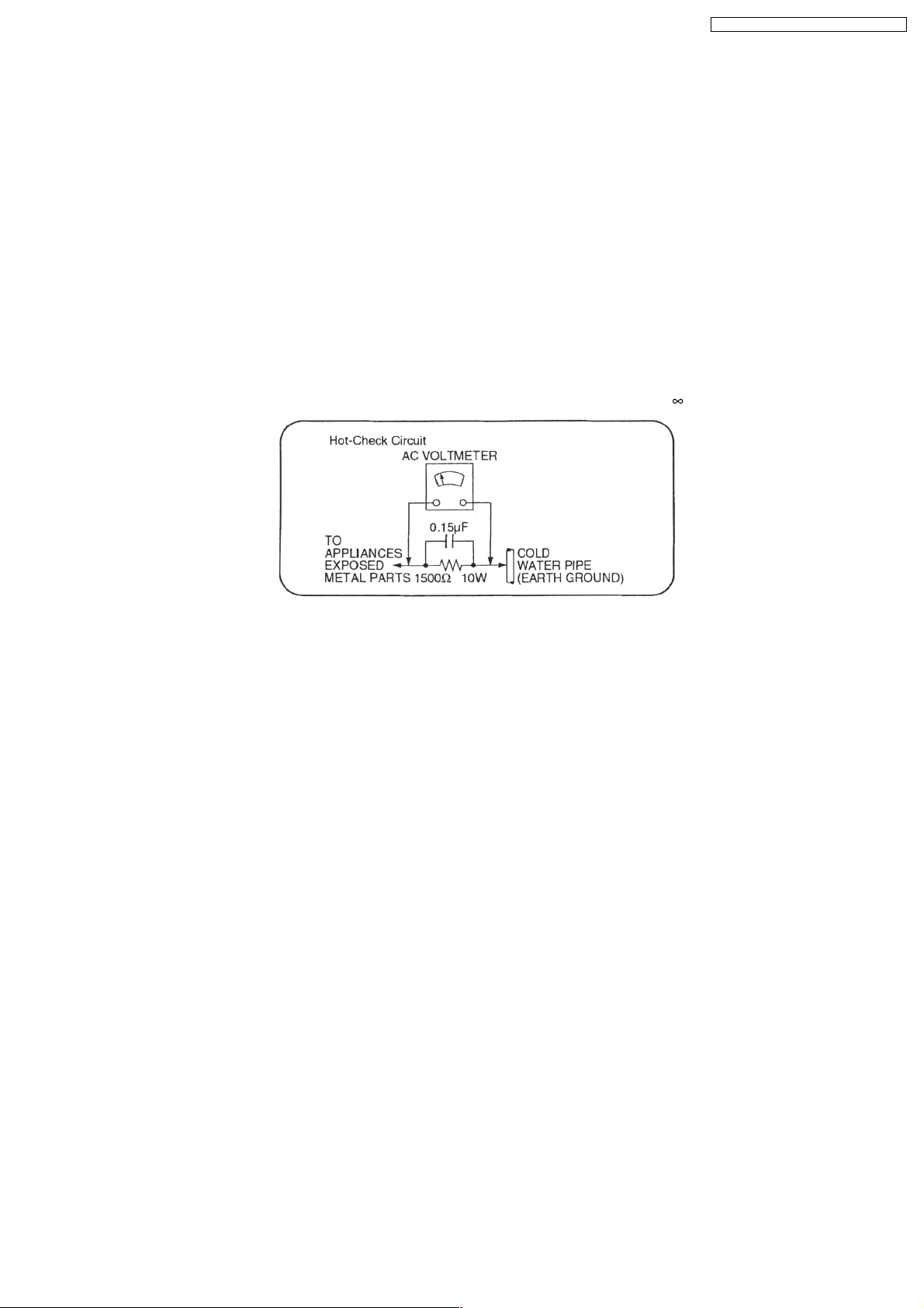
Fig. 1
1.1.2. LEAKAGE CURRENT HOT CHECK (See Figure 1.)
1. Plug the AC cord directly into the AC outlet. Do not use an isolation transformer for this check.
2. Connect a 1.5kΩ, 10 watts resistor, in parallel with a
good earth ground such as a water pipe, as shown in Figure 1.
3. Use an AC voltmeter, with 1000 ohms/volt or more sensitivity, to measure the potential across the resistor.
4. Check each exposed metallic part, and measure the voltage at each point.
5. Reverse the AC plug in the AC outlet and repeat each of the above measurements.
6. The potential at any point should not exceed 0.75 volts RMS. A leakage current tester (Simpson Model 229 or equivalent) may
be used to make the hot checks, leakage current must not exceed 1/2 milliamp. In case a measurement is outside of the limits
specified, there is a possibility of a shock hazard, and the equipment should be repaired and rechecked before it is returned to
the customer.
0.15µF capacitors, between each exposed metallic part on the set and a
3
SH-HT880WEB / SH-FX 50TEB / SE-FX50E B
2 Caution for AC Mains Lead
4

SH-HT880WEB / SH-FX 50TEB / SE-FX50E B
3 Handling the Lead-free Solder
3.1. About lead free solder (PbF)
Distinction of PbF P.C.B. :
P.C.B.s (manufactured) using lead free solder will have a PbF stamp on the P.C.B.
Caution:
· Pb free solder has a higher melting point than standard solder. Typically the melting point is 50 - 70°F (30 - 40°C) higher.
Please use a high temperature soldering iron. In case of the soldering iron with temperature control, please set it to 700 ± 20°F
(370 ± 10°C).
· Pb free solder will tend to splash when heated too high (about 1100°F/600°C).
· W hen soldering or unsoldering, please completely remove all of the solder on the pins or solder area, and be sure to heat the
soldering points with the Pb free solder until it melts enough.
4 Before Repair and Adjustment (Digital Receiver SE-FX50)
Disconnect AC power, discharge Power Supply Capacitors C5903 , C5904 , C5920 and C5926 through a 10 Ω, 1 W resistor to
ground.
DO NOT SHORT-CIRCUIT DIRECTLY (with a screwdriver blade, for instance), as this may destroy solid state devices.
After repairs are completed, restore power gradually using a variac, to avoid overcurrent.
Current consum ption at AC 230 - 240V, 50Hz in NO SIGNAL mode should be ~248 mA.
5 Protection Circuitry
The protection circuitry may have operated if either of the following conditions are noticed:
· No sound is heard when the power is turned on.
· Stops during a performance.
The function of this circuitry is to prevent circuitry damage if, for example, the positive and negative speaker connection wires are
“shorted”, or if speaker systems with an impedance less than the indicated rated impedance of the amplifier are used.
If this occurs, follow the procedure outlines below:
1. Turn off the power.
2. Determine the cause of the problem and correct it.
3. Turn on the power once again after one minute.
Note:
When the protection circuitry functions, the unit will not operate unless the power is first turned off and then on again.
5
SH-HT880WEB / SH-FX 50TEB / SE-FX50E B
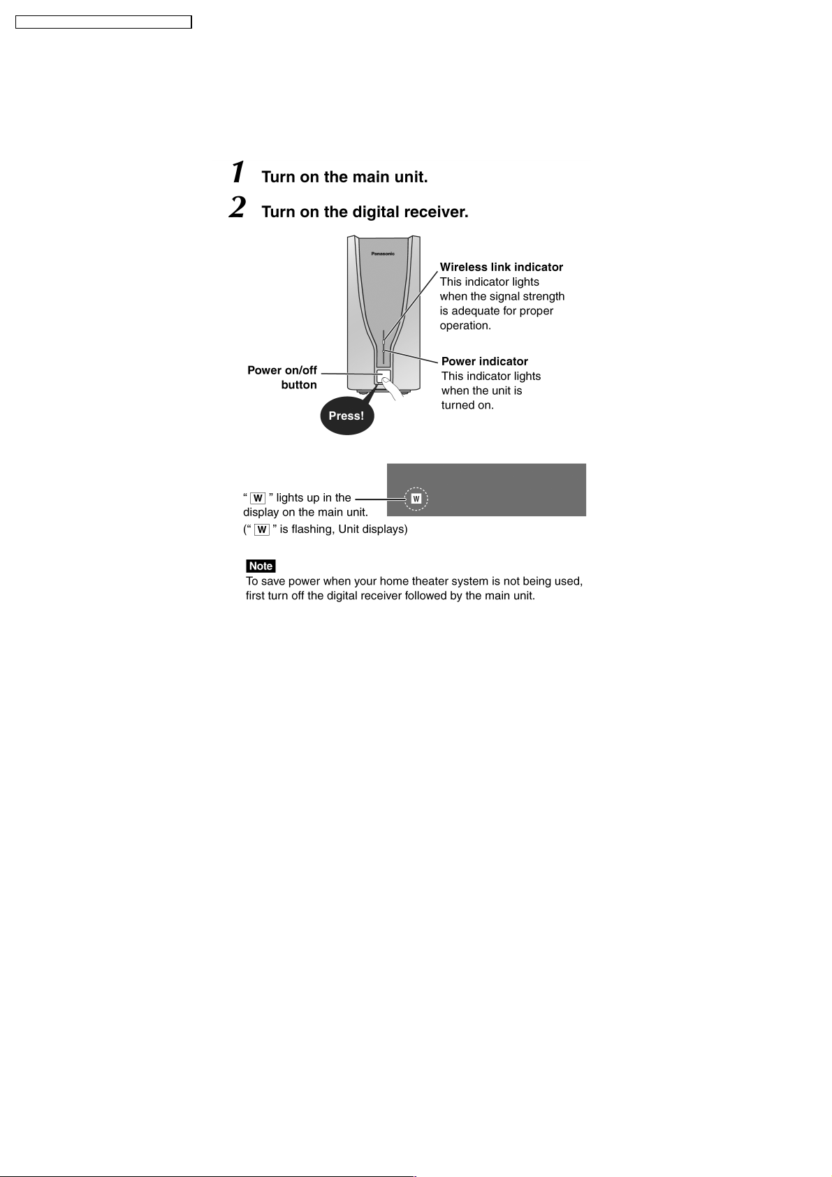
6 Using of Digital Receiver Unit (SE-FX50)
· This model can be equipped with the digital transmitter and receiver to enjoy surround sound wirelessly.
6.1. Below is tips on using the digital receiver
Special Note:
This unit is equipped with auto-off function (Relay will turn off the power after 1 minute to reduce power consumption).
6

6.2. Tips for using Digital Transmitter (SH-FX50T)
SH-HT880WEB / SH-FX 50TEB / SE-FX50E B
7
SH-HT880WEB / SH-FX 50TEB / SE-FX50E B
7 Technical Information (New Features)
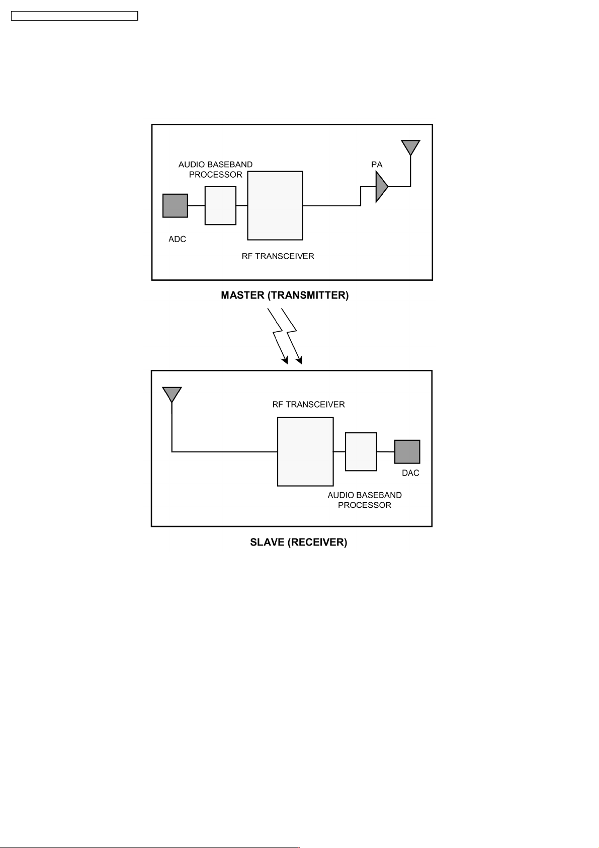
7.1. RF Wireless Audio Transceiver
7.1.1. Block Diagram
7.1.2. Definition
1. ADC : Analog-to-Digital Converter
2. Transceiver : Transmitter-Receiver Device
3. PA : Power Amplifier
4. DAC : Digital-to-Analog Converter
7.1.3. Features
· Crystal Clear CD Quality Stereo Sound
· Highly Robust Forward Error Correction
· 44.1KHz / 48KHz sampling frequency
· Adaptive Frequency Hopping System
· Range (open space) : 100m
· Low power consumption
· SNR (for left / right channel analog interface) : 80 dB
· THD : 0.2%
· Compact : 40mm x 80mm
8
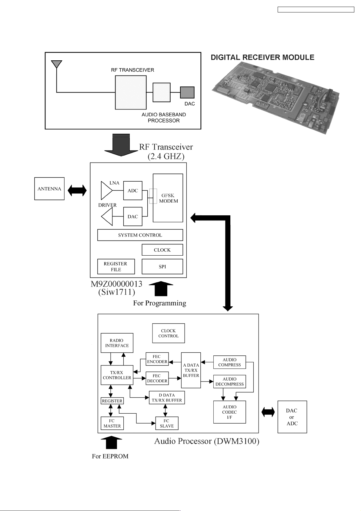
7.2. Detail Block Diagram (Receiver module)
SH-HT880WEB / SH-FX 50TEB / SE-FX50E B
9
SH-HT880WEB / SH-FX 50TEB / SE-FX50E B
7.2.1. Operation
RF signal transmission and reception:
During the receive process, the radio signal is taken from a pair of balanc ed RF I/O pins that feed into the low noise amplifier (LNA).
Direct I/Q down conversion and on-chip filtering send the processed I/Q data to the analog-to-digital converter before processing
by the GFSK (Gaussian Frequency Shift Keying) demodulator. Within the demodulator, data detection and timing recovery circuits
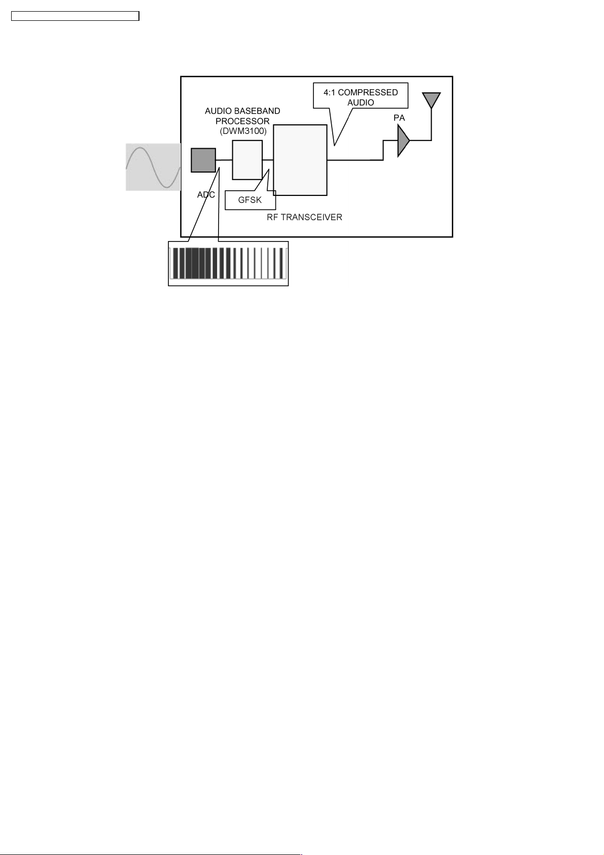
convert the data for transfer to an external device. The transmit process operates in a similar fashion in reverse order.
The transmitted signal is GFSK (Gaussian Frequency Shift Keying) modulated data that is amplified on the chip to yield a radiated
output of 0dBm. A power control signal for an external amplifier is provided.
The audio baseband processor (DWM3100) is a digital audio processor IC encompassing apt-XTM audio compress/decompress
algorithm for wireless transmission of crystal-clear CD quality audio data.
For digital transmission the analog audio signals are sampled at 48kHz and converted to 1.536Mbps digital data through an
external 16-bit stereo audio codec. The digitized data are apt-XTM 4:1 compressed to 384Kbps stream data for efficient
transmission. Redundancy bits for forward error correction (FEC), synchronization flags, and control signals for time-division
duplexing (TDD) are appended to form data frames for error-free transmission.
In the receiver(Slave), synchronization flags and control data are first detected from the input stream. FEC decoder corrects any
errors that may have been introduced during the transmission and produces error-free compressed audio data. The compressed
audio is decompressed into 16-bit stereo PCM audio data through digital signal processing blocks. External audio codec converts
the PCM data to 2-channel (left and right) analog audio signals.
The Tx/Rx controller is in charge of several functions such as radio channel setup, frequency hopping for interference reduction and
generation of control signal for TDD and external RF chip.
In audio mode, the transmitter(Master) can send additional 16Kbps digital data simultaneously with stereo audio data.
How much time delay to transmit audio in wireless?
Audio compression and decompression requires about 3ms. Total time delay can be calculated as follows: Total delay time = audio
compression time + transmitter operating time + receiver operating time + audio decompression time. Total delay time is
approximately 12.2ms.
What is the power consumption?
The 2.4GHz RF module consumes about 45mA (max 65mA) for the transmitter and 55mA (max 71mA) for the receiver. The
EEPROM consumes about 1mA while the baseband IC consumes about 20mA.The total power consum ption is 66mA (max 86mA)
for the transmitter and 76mA (max 92mA) for the receiver.
10
SH-HT880WEB / SH-FX 50TEB / SE-FX50E B
Does the system support any mode to save power consumption?
Yes, it has POWER SAVING SCAN mode. When the communication link is lost, the slave starts scanning procedure to re-establish
the link. If the slave cannot find the master within a certain amount of time (info stored in EEPROM), the slave automatically goes
into power saving scan mode.
How does the system handle interference from other 2.4GHz RF devices?
It adopts Adaptive Frequency Hopping Spread Spectrum (AHSS) technology to avoid interference.
How does the system handle interference from other 2.4GHz RF devices?
The system supports 3 types of Spread Spectrum. These are
1. FHSS - Frequency Hopping Spread Spectrum
2. AHSS - Adaptive Frequency Hopping Spread Spectrum
3. Fixed Chann el Mode
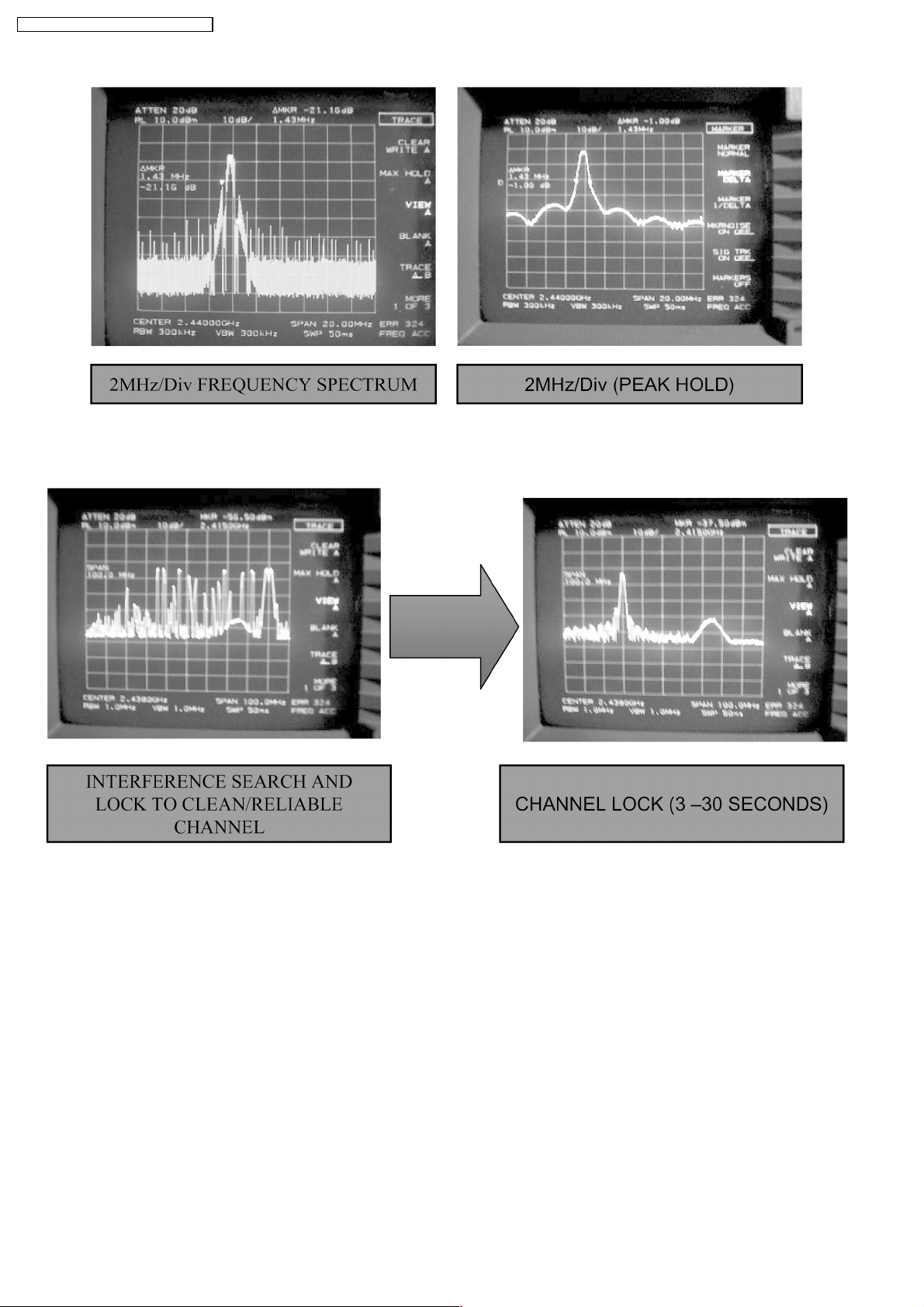
FHSS refers to the conventional 79 channels (or 23 dependent on the country) hopping of Bluetooth. Devices using such hoppin g
method receives a lot of interference from other devices that use 2.4GHz range frequency such as WLAN and other Bluetooth
devices. FHSS, being built to avoid interfering with other devices, rather interferes a lot with devices that has high output power
using 2.4GHz frequency range and with other FHSS devices.During initialization, system scans 79 channels (or 23) and selects the
clear, non-interfered and reliable channel and starts the communication between master and slave. During the channel link, the
channel becomes unreliable and the error detection from FEC block exceeds the preset error threshold value, the system executes
scanning, as in initialization, and reselects new clear and reliable channel.
FHSS and AHSS can be selected by setting appropriate parameters on the EEPRO M.
In Fixed Channel mode, 4 frequency levels can be selected (2.410GHz, 2.430GHz, 2.450GHz and 2.470GHz)
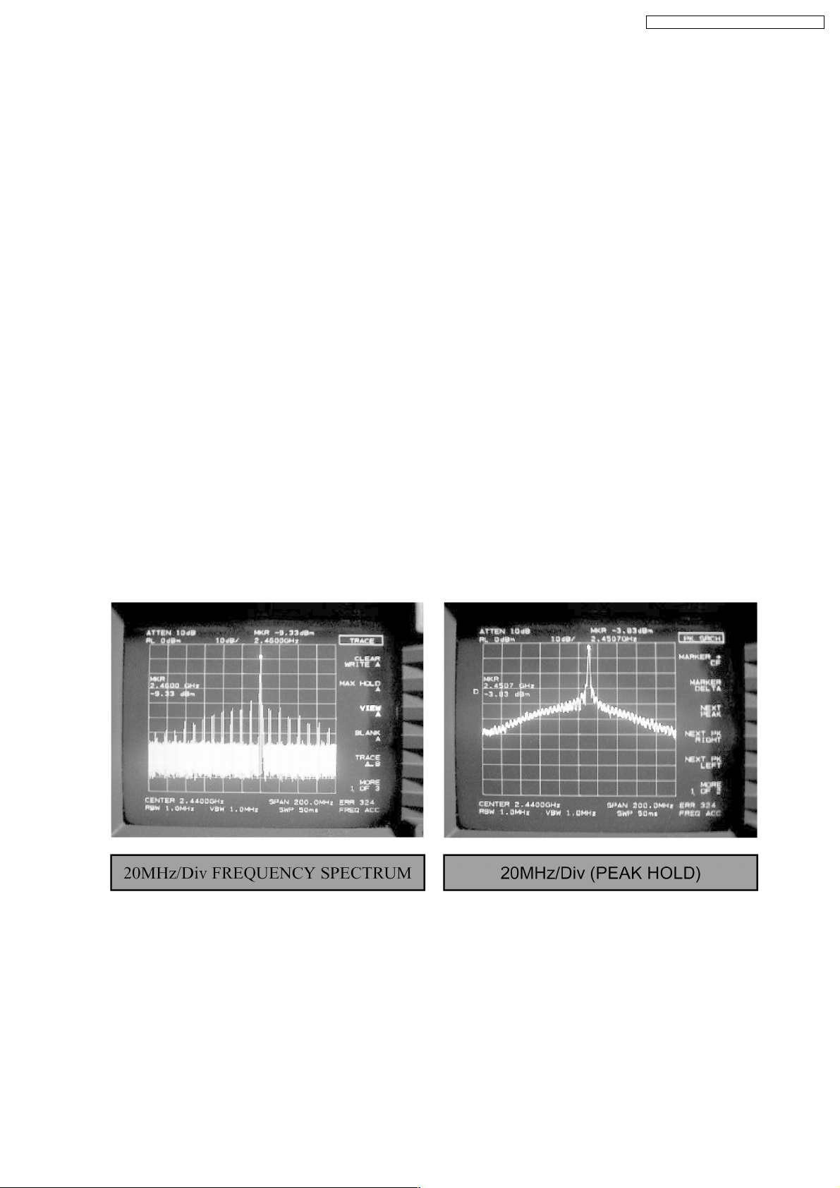
Spectrum distribution characteristic of 2.4GHz RF signal
11
SH-HT880WEB / SH-FX 50TEB / SE-FX50E B
Spectrum distribution characteristic of 2.4GHz RF signal
How can Master or Slave setting be selected? By software or hardware?
It can be selected by external control pin.
How long does it take to transmit single packet?
To establish communication channel properly, hopping frequency and Syncword of each packet should be determined by Device
ID(Identification). Device ID is unique value of each device, master and slaves. Only master and slaves with same Device ID can
communicate each other. Device ID can be set manually in case selected master and slaves do not communicate together. This
procedure is *Device ID set*. Device ID set procedure occurs when master and slave devices boot simultaneously with ID_SET=1.
In this procedure, the slave can figure out the Device ID of the master and store it in external EEPROM.When ID_SET is
established, S5G3000 performs ID send/scan to send Device ID of master to slave before general page operation. In normal mode,
communication is accomplished by going into page state directly without ID send/scan.
How can the Master and Slave units be paired to prevent mix-up?
It takes 2.5ms.
12
SH-HT880WEB / SH-FX 50TEB / SE-FX50E B
7.3. Class-D Amplifier
7.3.1. How are digital amplifiers different?
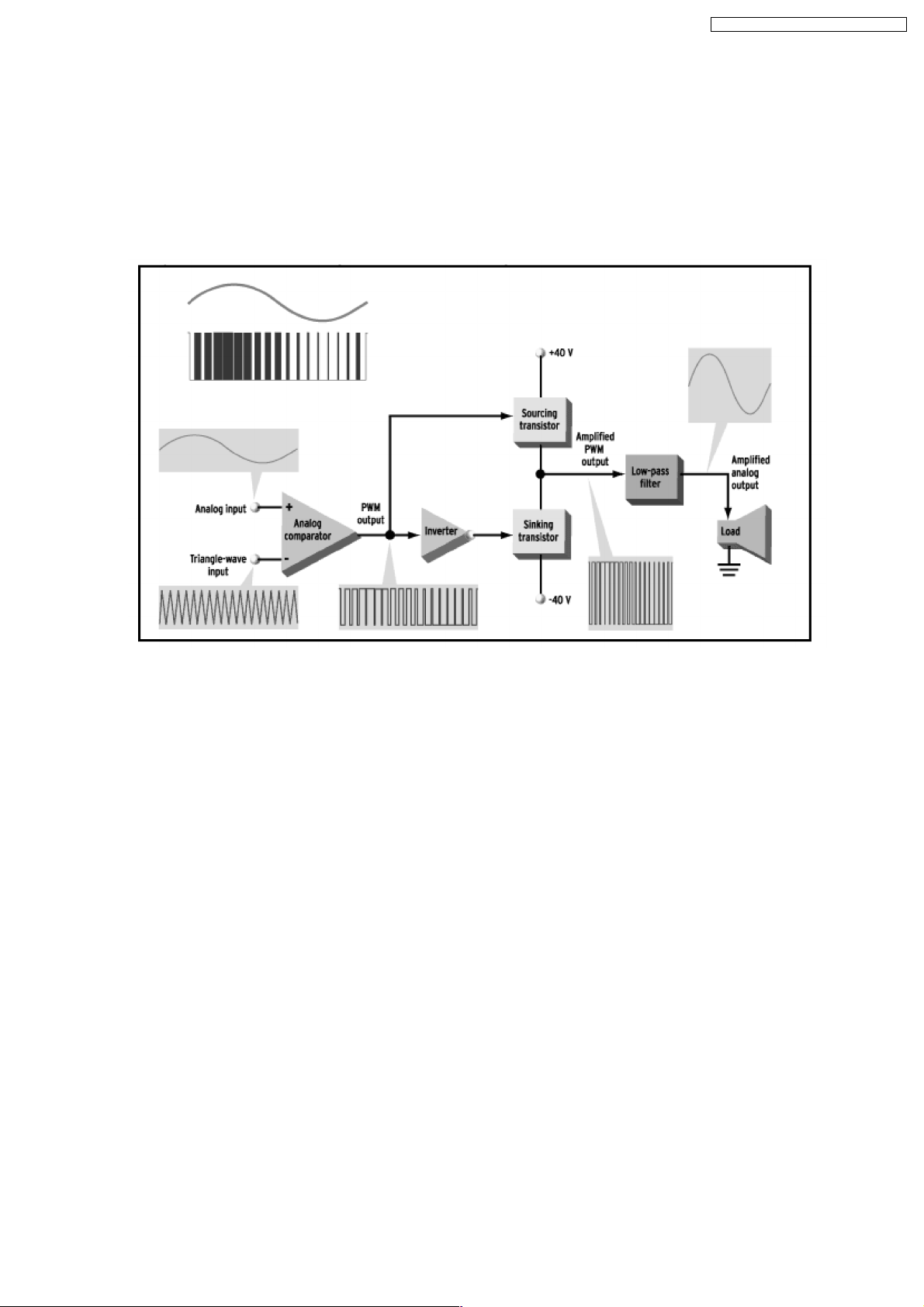
A digital amplifier incorporates a switching output stage that operates according to a principle known as pulse width modulation
(PWM). In contrast to the low-frequency control signal used in a conventional analog amplifier output stage, the switching output
stage of a digital amplifier is controlled by a high-frequency digital signal. The high-frequency digital signal is a PWM signal, in
which the music is modulated into a fixed-frequency carrier signal. In a digital amplifier, the modulation process is based on a digital
pulse code modula ted (PCM) representation of the music signal (or other signal that needs amplification) from a CD player, a DVD
player, or some other device.
BLOCK DIAGRAM OF TYPICAL ANALOG INPUT CLASS-D AMPLIFIER
7.3.2. What are the advantages of digital amplification technology?
· High power efficiency, i.e., smaller heat sinks and/or no fan required
· Compact (reduced PCB area)
· Low weight (reduced transformer size)
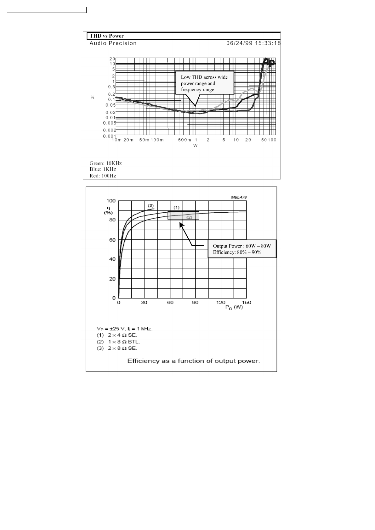
· Good sound quality (low signal distortion/THD)
7.3.3. Why is the digital amplifier so efficient?
A class-D amplifier is one in which the output transistors are operated as switches. When a transistor is off, the current through it
is zero. When it is on, the voltage across it is small, ideally zero. In each case, the power dissipation is very low.
7.3.4. Does the “D” in class-D mean DIGITAL?
No. This is not correct because the operation of the class-D amplifier is based on analog principles. There is no digital coding of
the signal. Before the advent of the class-D amplifier, the standard classes were class-A, class-AB, class-B, and class-C. The “D”
is simply the next letter in the alphabet after “C.” Indeed, the earliest work on class-D amplifiers involved vacuum tubes and can
be traced to the early 1950s.
13
SH-HT880WEB / SH-FX 50TEB / SE-FX50E B
7.3.5. What are the potential problems of a Class-D amplifier based system?
The two most common issues of class-D amp system are AM interference and EMI.The switching frequency of class-D ranges from
300kHz to 450kHz typically 315kHz. The harmonics of such switching frequency will fall into the AM band of 600kHz to 1710kHz.
To avoid interference, it is recommended to have a variable switching frequency adjustment circuit [usually known as beatproofing
in PSG). Systems without AM tuner are not required to have such circuitry.
14
SH-HT880WEB / SH-FX 50TEB / SE-FX50E B
Class-D amp systems are basically switching systems. As such, it is prone to EMI. EMI issues can be rectified through proper
grounding techniques and proper components layout. It is quite common to see ferrite beads, capacitors and inducto rs on these
systems.
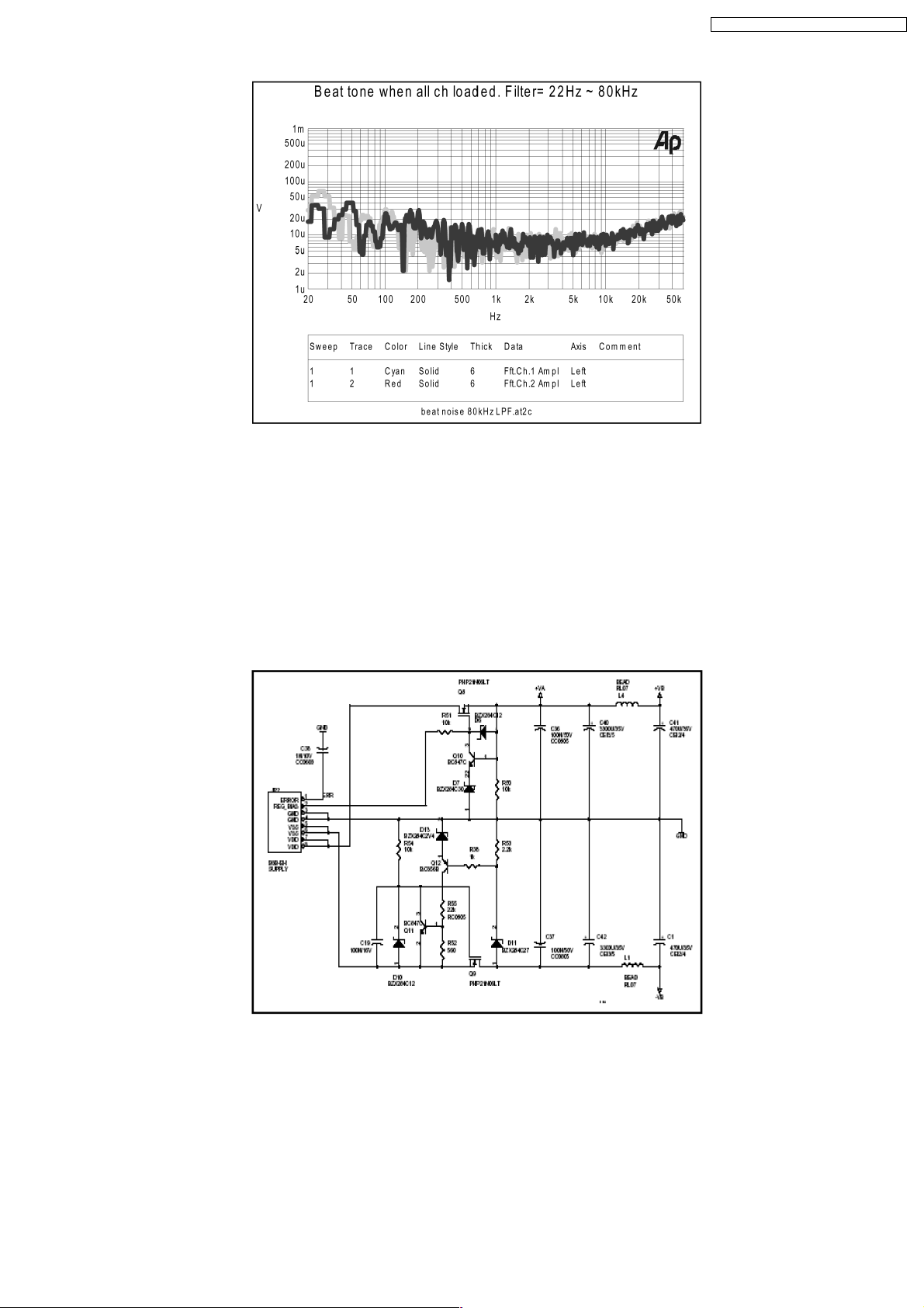
Another issue would be interchannel modulation. This problem would only arise if each channe l is using different switching
frequency. It would create an amplified “beat” that can be heard from speakers.
7.3.6. Other issues should we be aware of ?
The class-D amplifier IC is limited to only +/- 30volts power supply . This system uses a linear power source to supply power to the
module. These linear power supplies are unregulated (i.e. voltage is not fixed). Therefore we have to implement a voltage limiter
circuit that would limit the maximum voltage of +/-27volts. It is also imperative that the power supply voltages are almost balanced.
Also, the class-D amplifier IC is configured as single-ended connection. It means one of the outputs is a signal while the other is
connected to ground. With this configuration, this Class D amplifiers will deliver energy back to the power supply. We refer to this
phenomenon as “Supply pumping effect”. Supply pumping effect is more evident on very low frequencies. It is recommended to
have enough buffer on the supply rails to limit the supply pumping effect.It is also advised not to use any type of speakers for
testing. There is an output filter that needs to be matched with the intended speaker. A normal resistive load may be used.
7.3.7. Actual Class-D amplifier IC information
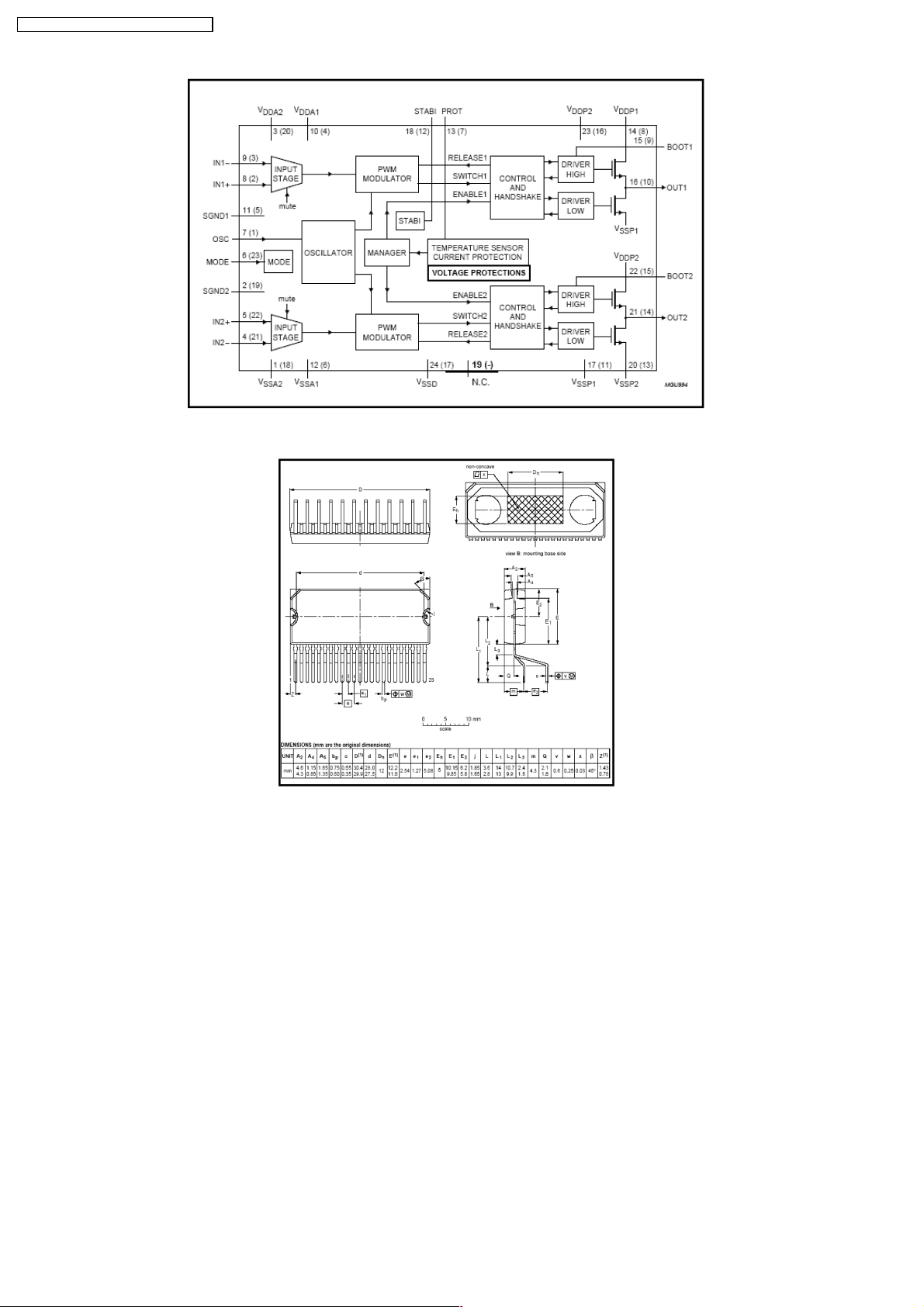
Part number: C1BA0 0000407 (TDA8920BJ)
Block diagram:
15
SH-HT880WEB / SH-FX 50TEB / SE-FX50E B
IC Package Information
Soldering Information
Wave Soldering/Dipping: The maximum permissible temperature of the solder is 260 ーC; solder at this temperature must not be in
contact with the joints for more than 5 seconds. The total contact time of successive solder waves must not exceed 5
seconds.Manual Soldering: If the temperature of the soldering iron bit is less than 300 ーC it may remain in contact for up to 10
seconds. If the bit temperature is between 300 and 400 ーC, contact may be up to 5 seconds.
16
8 TX & RX Module P.C.B.
8.1. TX and RX Inspection Layout
· The following processes is required when
1. EEPROM IC was replaced due to fault.
2. Replacement of RF components (Refer to section 8.2 for list of RF components.)
SH-HT880WEB / SH-FX 50TEB / SE-FX50E B
17
SH-HT880WEB / SH-FX 50TEB / SE-FX50E B
8.1.1. TX and RX Inspection Process
Below is a list equipments & softwares needed:
1. Test jig (For component level repair & replacement) [M]
2. Frequency spectrum analyser (3 GHZ Range: Recommend)
3. Personal computer (Hyper Terminal)
4. Load EEPROM_I.O. exe (EEPROM / FIRMWARE DOWNLOADING) [M]
5. Program IDI.O. exe (ID programming)
6. Service jig Part no: (RFKZFX50PP-S) [M]
Note:
Item 1 to 5 as mentioned applies during component level repair. Item 6 is used for purpose of verification the functionality of TX
& RX.
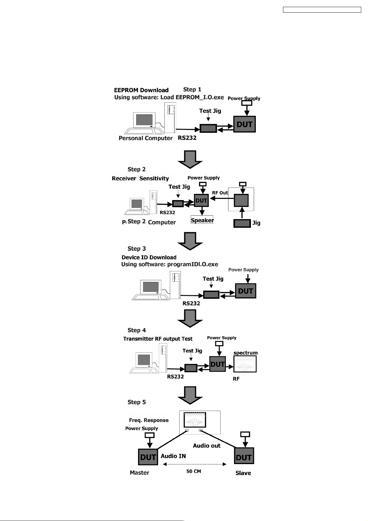
Step 1: EEPROM Download
To download Parameters & Status into the Registers of Baseband IC. (IC3 - DWM3100)
Step 2: Receiver Sensitivity
To ensure the communication distance between master & slave of at least 100m. (Ref to BER test at section 8.4)
Step 3: Device ID Programming
To program into both the Master (Transmitter Module) & Slave (Receiver Module) an unique number so as not to interfere with the
communication between one unit with another.
Note:
For ID No. please refer to indication on the modules P.C.B. (Ref to section 13.3 and 13.4)
Step 4: Transmitter RF Output Test
To ensure the Transmitting Power is within 11 to 16dBM (At center freq = 2.441GHZ, Span = 100MH Z, Ref Level = +25dBM)
Step 5: Audio Frequency Response Measurement
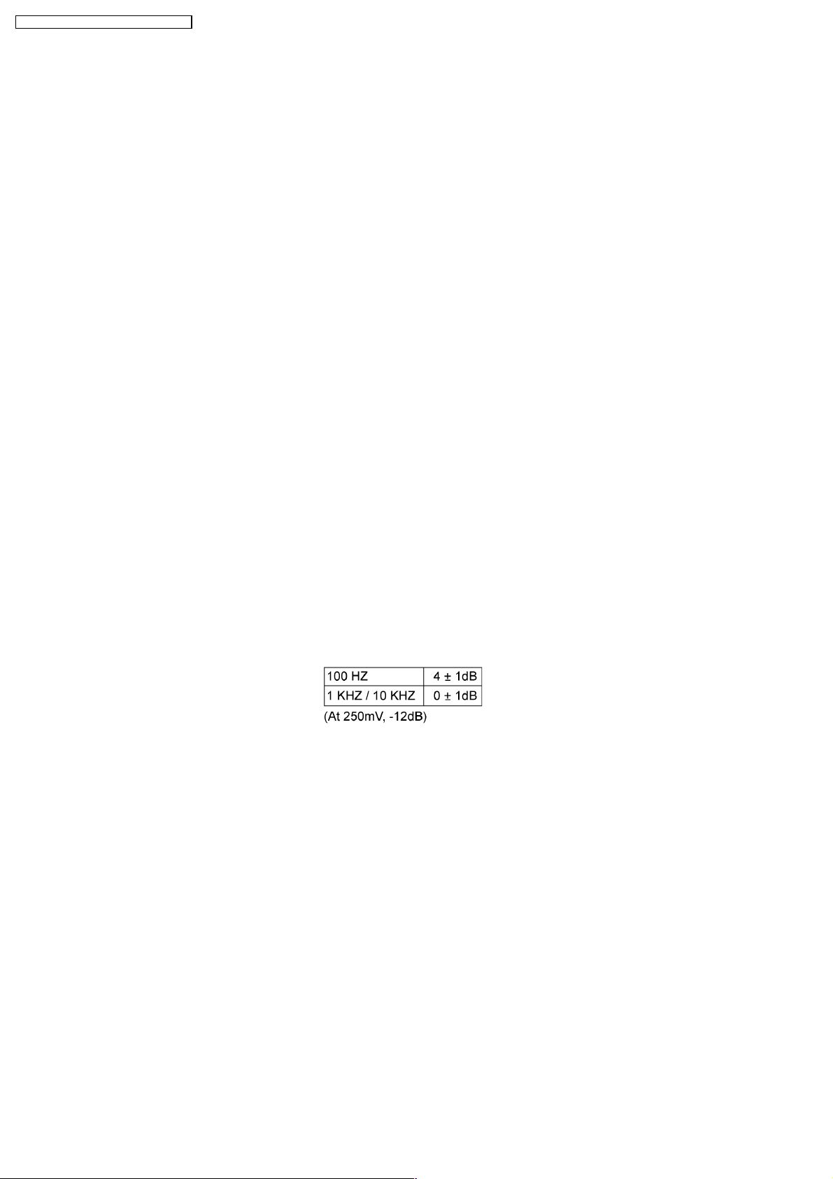
To ensure the frequency response of the unit as below:
8.2. List of RF components
Below is the list of RF components that need special care (handling) during replacement of parts:
· AN1 - chip dielectric antenna
· J1 - Microwave coaxial connector
· FL1 - LC Filter
· IC2 - RF Transceiver
· IC1 - RF Power Amplifier
· IC3 - Audio Processor IC
· SW1 - RF switch
Note:
Please refer to electrical partlist (section 18.3. and 18.4.) for part no. For location of these components, please refer to section
13.1.
18
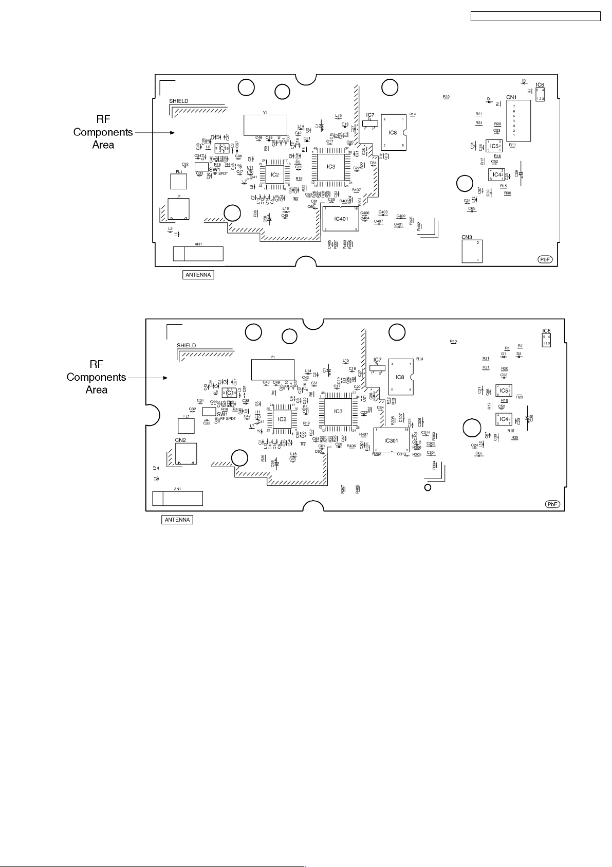
8.2.1. Component Layer side A (Receiver Module P.C.B.)
8.2.2. Component Layer side A (Transmitter Module P.C.B.)
SH-HT880WEB / SH-FX 50TEB / SE-FX50E B
8.3. RF Transmit Power Test
Note:
This test is carried out & necessary for component level repair / replacement.
8.3.1. Procedure
Step 1 : Put PCB properly on the inspection jig and connect RF cable into the PCB.
19
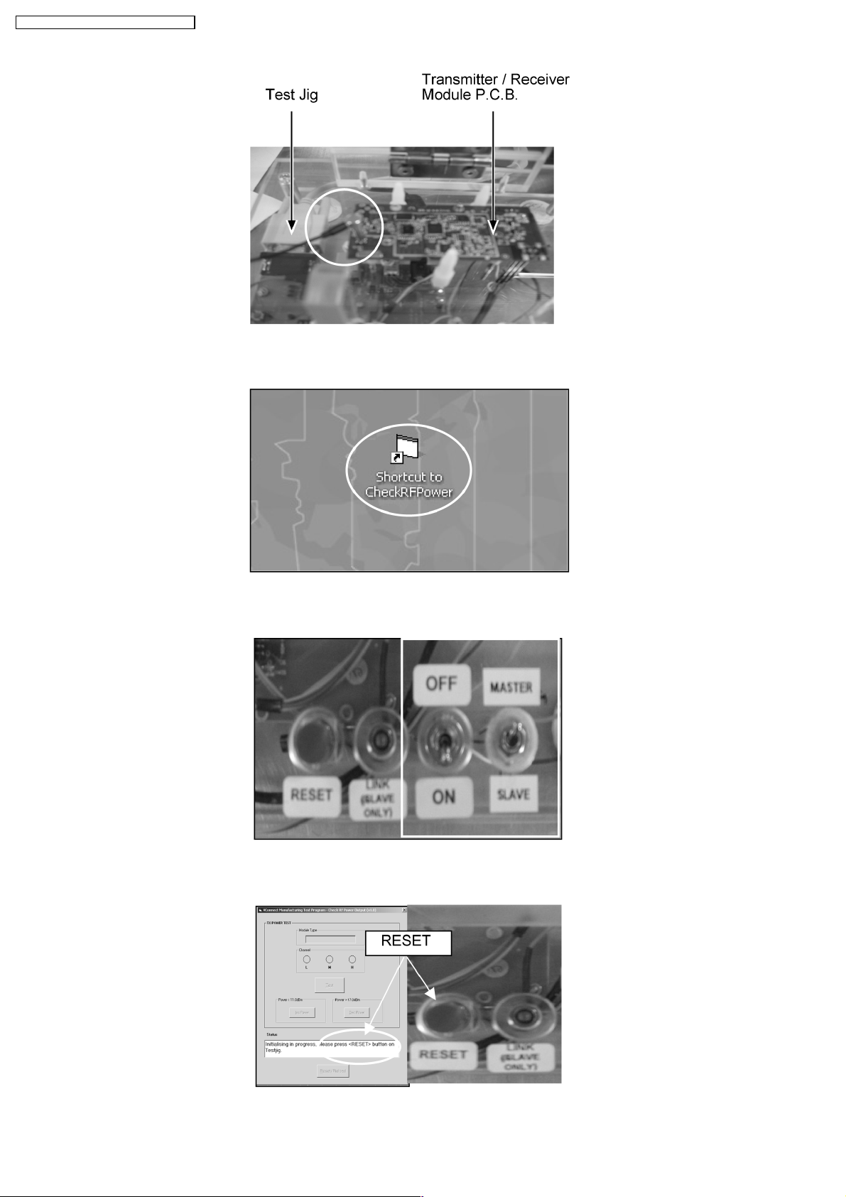
SH-HT880WEB / SH-FX 50TEB / SE-FX50E B
Step 2 : Select EEPRO M programming icon.
Step 3 : On the switch and according to the PCB BLOCK NO select slave (A) or master (B) module .
Step 4 : Follow the reset information, press reset button.
20
SH-HT880WEB / SH-FX 50TEB / SE-FX50E B
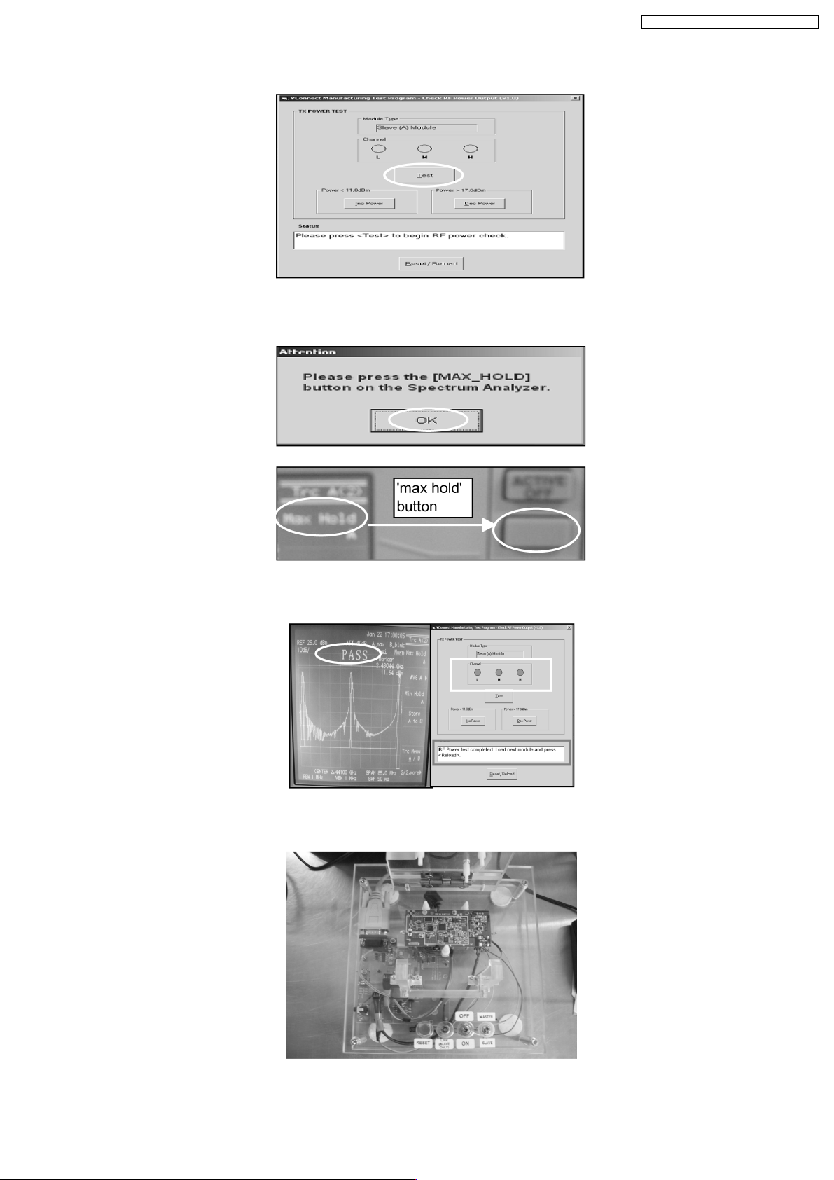
Step 5 : Press ´Test´ icon
Step 6 : When the ´max_hold´ info shown, press max_hold´ button on the spectrum analyzer, then press ´OK´ icon.
Step 7 : Base on the Fail or Pass information on the spectrum analyzer to judge PCB condition.
Step 8 : OFF the switch, take out the PCB from jig and put marking.
21
 Loading...