

Panasonic SEFX-61-GN, SHHT-995-WGN Service manual
Specification
n WIRELESS SYSTEM AND DIGITAL TRANSCEIVER
Power supply AC 230-240 V, 50 Hz
Power consumption
Digital transceiver (SH-FX80T) 0.85 W
Wireless system (SE-FX61) 30 W
Dimensions (W x H x D)
Digital transceiver (SH-FX80T) 97 mm x 47.5 mm x 8.5 mm
Wireless system (SE-FX61) 89 mm x 189 mm x 180 mm
Mass
Digital transceiver (SH-FX80T) 0.03 kg
Wireless system (SE-FX61) 0.7 kg
Wireless module
Frequency range 2.403-2.425 GHz
No. of channels 23
Operating temperature range +5 °C to +35 °C
Operating humidity range 5 % to 90 % RH (no condensation)
Power consumption in standby mode : approx. 4 W
n System : SC-HT995WGNS
Music Center : SA-HT995WGNS
Front Speaker : SB-FS990E-S
Surround Speaker : SB-FS540E1-
Center Speaker : SB-PC895GC-S
Subwoofer : SB-W895GC-S
Digital Tx & Rx System : SH-
HT995WGNS
ORDER NO. MD0605202CE
Digital Transmitter & Receiver
SH-HT995WGN
SE-FX61GN
SH-FX80TGN
Colour
(S)..........Silver Type
Notes:
1. Specifications are subject to change without notice.
Mass and dimensions are approximate
2. Total harmonic distortion is measured by a digital spectrum
analyzer
Power supply:
This model uses Switching Mode Power Supply (SMPS) Module for
powering the receiver unit. It is replaceable as an assembly unit.
S
© 2006 Matsushita Electric Industrial Co. Ltd.. All
rights reserved. Unauthorized copying and
distribution is a violation of law.
SH-HT995WGN
CONTENTS
Page Page
1 Safety Precautions 3
1.1. GENERAL GUIDELINES
1.2. Before Repair and Adjustment (Digital Receiver SE-
FX61GN)
1.3. Protection Circuitry
2 Prevention of Electro Static Discharge (ESD) to
Electrostatically Sensitive (ES) Devices
3 Handling the Lead-free Solder
3.1. Service caution based on legal restrictions
4 Accessories
5 Using of Digital Receiver Unit
5.1. Connecting the digital transceiver (SH-FX80TGN)
5.2. Connecting the surround speaker cables to the wireless
system (SE-FX61GN)
5.3. AC Power Cord connection (SE-FX61GN)
5.4. Making the wireless link (SE-FX61GN)
6 Technical Information (Wireless Surround)
6.1. RF Wireless Audio Transceiver
6.2. Detail Block Diagram (Receiver module)
6.3. Class-D Amplifier
7 Assembling and Disassembling
7.1. Note
7.2. Disassembly flow chart (For SE-FX61GN)
7.3. Main Parts Location Diagram
7.4. Disassembly of Wireless System (SE-FX61GN)
7.5. Disassembly of Digital Transceiver (SH-FX80TGN)
8 Service Positions
8.1. Checking of Led and Receiver Module P.C.B.
8.2. Checking of Digital Amp and SMPS Module Unit
9 Service Hint
9.1. Use of Service Jig (RFKZFX50PP-S)
9.2. Procedures for testing of link between digital transmitter &
receiver
9.3. Troubleshooting Guide for Wireless Surround Speaker
10 Service parts replacement
3
3
4
5
6
6
7
8
8
8
8
9
10
10
11
15
18
18
19
19
20
25
28
28
29
30
30
31
33
10.1. Replacement of P.C.B.
10.2. Replacement of Transmitter Assembly
10.3. ID Location
10.4. Digital Transceiver Card Service Assembly
(RFKVHFX80TE)
11 Voltage Measurement
11.1. DIGITAL AMP P.C.B.
11.2. LED P.C.B.
12 Wiring Connection Diagram
13 Block Diagram
13.1. DIGITAL AMP MODULE BLOCK
13.2. RECEIVER MODULE BLOCK
13.3. TRANSIMITTER MODULE BLOCK
14 Notes of Schematic Diagram
15 Schematic Diagram
15.1. DIGITAL AMP CIRCUIT and LED CIRCUIT
15.2. RECEIVER MODULE CIRCUIT
15.3. TRANSMITTER MODULE CIRCUIT
16 Printed Circuit Board Diagram
16.1. DIGITAL AMP P.C.B and LED P.C.B
16.2. RECEIVER MODULE P.C.B and TRANSMITTER
MODULE P.C.B
17 Illustration of IC's, Transistors and Diodes
18 Terminal Functions of Integrated Circuits
18.1. IC12 (M9Z000000013): IC RF
19 Exploded Views
19.1. Cabinet Parts Location
19.2. Packaging
19.3. Main Unit Packaging
20 Replacement Parts List
20.1. Parts List (SE-FX61GN)
20.2. Parts List (SH-FX80TGN)
35
35
35
36
37
38
38
38
39
41
41
42
43
45
47
47
48
50
53
53
54
55
56
56
57
57
58
59
60
60
62
2
SH-HT995WGN
1 Safety Precautions
1.1. GENERAL GUIDELINES
1. When servicing, observe the original lead dress. If a short circuit is found, replace all parts which have been overheated or
damaged by the short circuit.
2. After servicing, see to it that all the protective devices such as insulation barriers, insulation papers shields are properly
installed.
3. After servicing, make the following leakage current checks to prevent the customer from being exposed to shock hazards.
1.1.1. LEAKAGE CURRENT COLD CHECK
1. Unplug the AC cord and connect a jumper between the two prongs on the plug.
2. Measure the resistance value, with an ohmmeter, between the jumpered AC plug and each exposed metallic cabine t part on
the equipment such as screwheads, connectors, control shafts, etc. When the exposed metallic part has a return path to the
chassis, the reading should be between 1MΩ and 5.2Ω.
When the exposed metal does not have a return path to the chassis, the reading must be
.
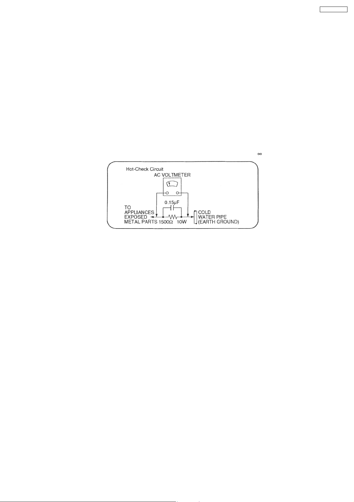
Figure. 1
1.1.2. LEAKAGE CURRENT HOT CHECK (See Figure 1.)
1. Plug the AC cord directly into the AC outlet. Do not use an isolation transformer for this check.
2. Connect a 1.5kΩ, 10 watts resistor, in parallel with a 0.15µF capacitors, between each exposed metallic part on the set and a
good earth ground such as a water pipe, as shown in Figure 1.
3. Use an AC voltmeter, with 1000 ohms/volt or more sensitivity, to measure the potential across the resistor.
4. Check each exposed metallic part, and measure the voltage at each point.
5. Reverse the AC plug in the AC outlet and repeat each of the above measurements.
6. The potential at any point should not exceed 0.75 volts RMS. A leakage current tester (Simpson Model 229 or equivalent) may
be used to make the hot checks, leakage current must not exceed 1/2 milliamp. In case a measurement is outside of the limits
specified, there is a possibility of a shock hazard, and the equipment should be repaired and rechecked before it is returned to
the customer.
1.2. Before Repair and Adjustment (Digital Receiver SE-FX61GN)
This model uses switching mode power supply (SMPS) module to provide the necessary voltages for the receiver (SE-FX61GN)
DO NOT SHORT-CIRCUIT DIRECTLY (with a screwdriver blade, for instance), as this may destroy solid state devices.
After repairs are completed, restore power gradually using a variac, to avoid overcurrent.
Current consum ption at AC 230-240V, 50Hz in NO SIGNAL mode should be ~150 mA.
This model uses the switching mode power supply unit (SMPS) to provide necessary voltage supply for powering.
3

SH-HT995WGN
1.3. Protection Circuitry
The protection circuitry may have operated if either of the following conditions are noticed:
· No sound is heard when the power is turned on.
· Stops during a performance.
The function of this circuitry is to prevent circuitry damage if, for example, the positive and negative speaker connection wires are
“shorted”, or if speaker systems with an impedance less than the indicated rated impedance of the amplifier are used.
If this occurs, follow the procedure outlines below:
1. Turn off the power.
2. Determine the cause of the problem and correct it.
3. Turn on the power once again after one minute.
Note:
When the protection circuitry functions, the unit will not operate unless the power is first turned off and then on again.
4
SH-HT995WGN
2 Prevention of Electro Static Discharge (ESD) to
Electrostatically Sensitive (ES) Devices
Some semiconductor (solid state) devices can be damaged easily by electricity. Such components commonly are called
Electrostatically Sensitive (ES) Devices. Examples of typical ES devices are integrated circuits and some field-effect transistors and
semiconductor “chip” components. The following techniques should be used to help reduce the incidence of component damage
caused by electro static discharge (ESD).
1. Immediately before handling any semiconductor component or semiconductor-equiped assembly, drain off any ESD on your
body by touching a known earth ground. Alternatively, obtain and wear a commercially available discharging ESD wrist strap,
which should be removed for potential shock reasons prior to applyin g power to the unit under test.
2. After removing an electrical assembly equiped with ES devices, place the assembly on a conductive surface such as aluminium
foil, to prevent electrostatic charge build up or exposure of the assembly.
3. Use only a grounded-tip soldering iron to solder or unsolder ES devices.
4. Use only an anti-static solder removal device. Some solder removal devices not classified as “anti-static (ESD protected)” can
generate electrical charge to damage ES devices.
5. Do not use freon-propelled chemicals. These can generate electrical charges sufficient to damage ES devices.
6. Do not remove a replacement ES device from its protective package until immediately before you are ready to install it. (Most
replacement ES devices are packaged with leads electrically shorted together by conductive foam, aluminium foil or
comparable conductive material).
7. Immediately before removing the protective material from the leads of a replacement ES device, touch the protective material
to the chassis or circuit assembly into which the device will be installed.
Caution
Be sure no power is applied to the chassis or circuit, and observe all other safety precautions.
8. Minimize bodily motions when handling unpackaged replacement ES devices. (Otherwise harmless motion such as the
brushing together of your clothes fabric or the lifting of your foot from a carpeted floor can generate static electricity (ESD)
sufficient to damage an ES device).
5
SH-HT995WGN
3 Handling the Lead-free Solder
3.1. Service caution based on legal restrictions
3.1.1. General description about Lead Free Solder (PbF)
The lead free solder has been used in the mounting process of all electrical components on the printed circuit boards used for this
equipment in considering the globally environmental conservation.
The normal solder is the alloy of tin (Sn) and lead (Pb). On the other hand, the lead free solder is the alloy mainly consists of tin
(Sn), silver (Ag) and Copper (Cu), and the melting point of the lead free solder is higher approx.30 degrees C (86°F) more than that
of the normal solder.
Definition of PCB Lead Free Solder being used
The letter of “PbF” is printed either foil side or components side on the PCB using the lead free solder.
(See right figure)
Service caution for repair work using Lead Free Solder (PbF)
· The lead free solder has to be used when repairing the equipment for which the lead free solder is used.
(Definition: The letter of “PbF” is printed on the PCB using the lead free solder.)
· To put lead free solder, it should be well molten and mixed with the original lead free solder.
· Remove the remaining lead free solder on the PCB cleanly for soldering of the new IC.
· Since the melting point of the lead free solder is higher than that of the normal lead solder, it takes the longer time to melt
the lead free solder.
· Use the soldering iron (more than 70W) equipped with the temperature control after setting the temperature at 350±30
degrees C (662±86°F).
Recommended Lead Free Solder (Service Parts Route.)
· The following 3 types of lead free solder are available through the service parts route.
RFKZ03D01K-----------(0.3mm 100g Reel)
RFKZ06D01K-----------(0.6mm 100g Reel)
RFKZ10D01K-----------(1.0mm 100g Reel)
Note
* Ingredient: Tin (Sn), 96.5%, Silver (Ag) 3.0%, Copper (Cu) 0.5%, Cobalt (Co) / Germanium (Ge) 0.1 to 0.3%
6

4 Accessories
Note : Refer to Packing Materials & Accessories Parts List (Section 20) for the part number.
AC Main Lead
SH-HT995WGN
7
SH-HT995WGN
5 Using of Digital Receiver Unit
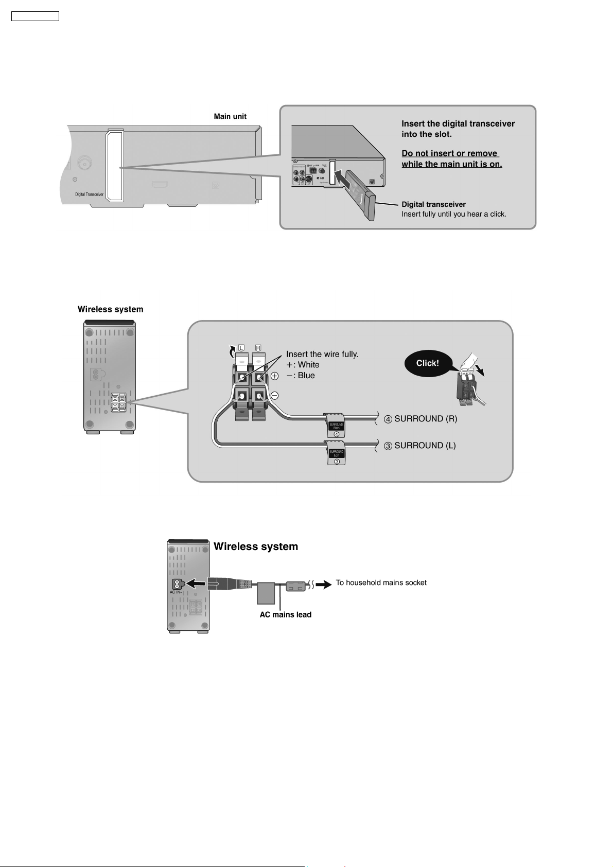
5.1. Connecting the digital transceiver (SH-FX80TGN)
5.2. Connecting the surround speaker cables to the wireless system
(SE-FX61GN)
5.3. AC Power Cord connection (SE-FX61GN)
8
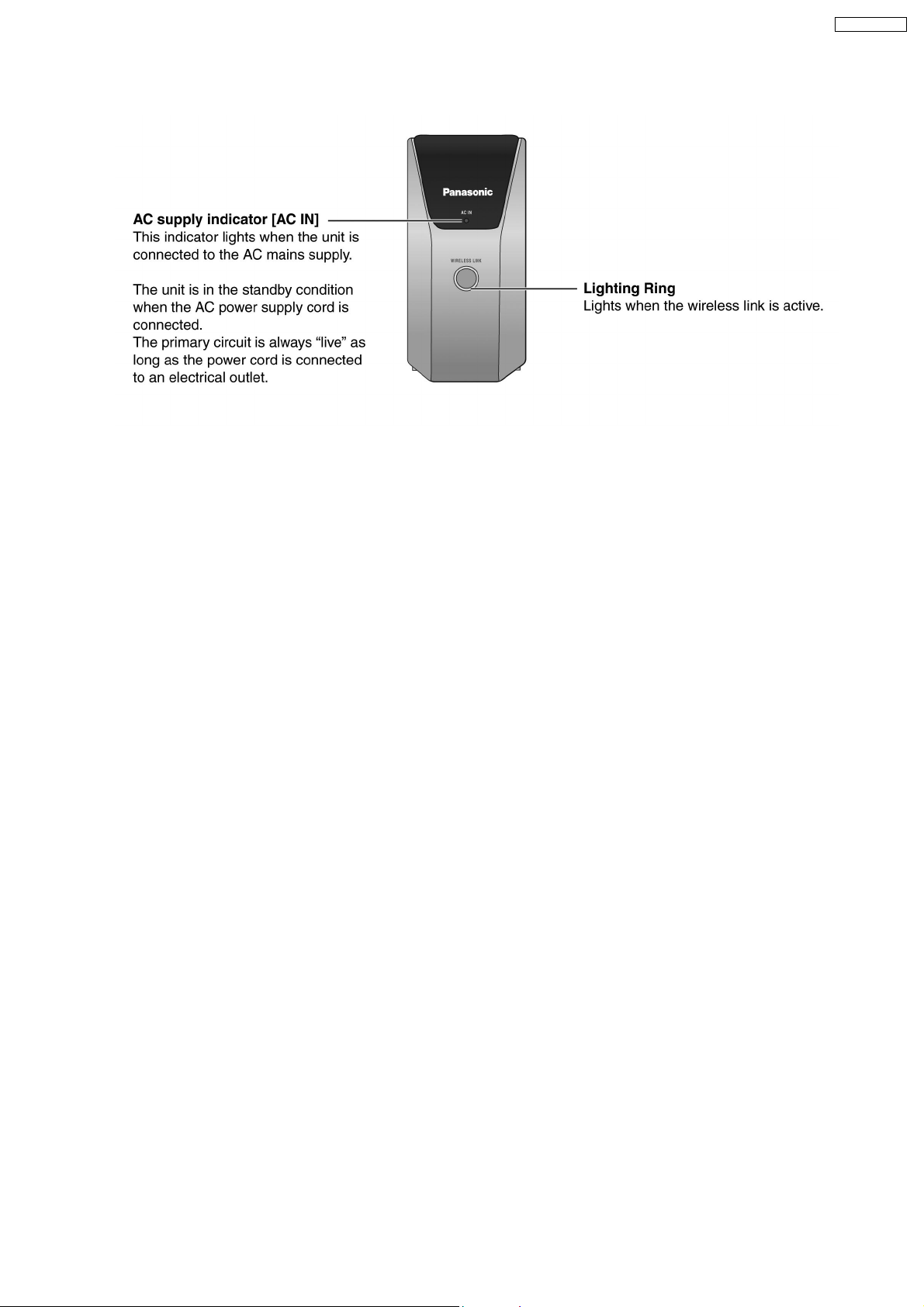
5.4. Making the wireless link (SE-FX61GN)
SH-HT995WGN
9
SH-HT995WGN
6 Technical Information (Wireless Surround)
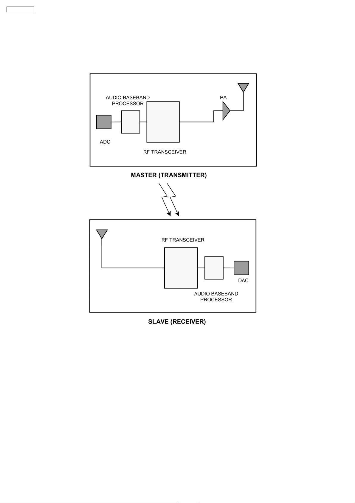
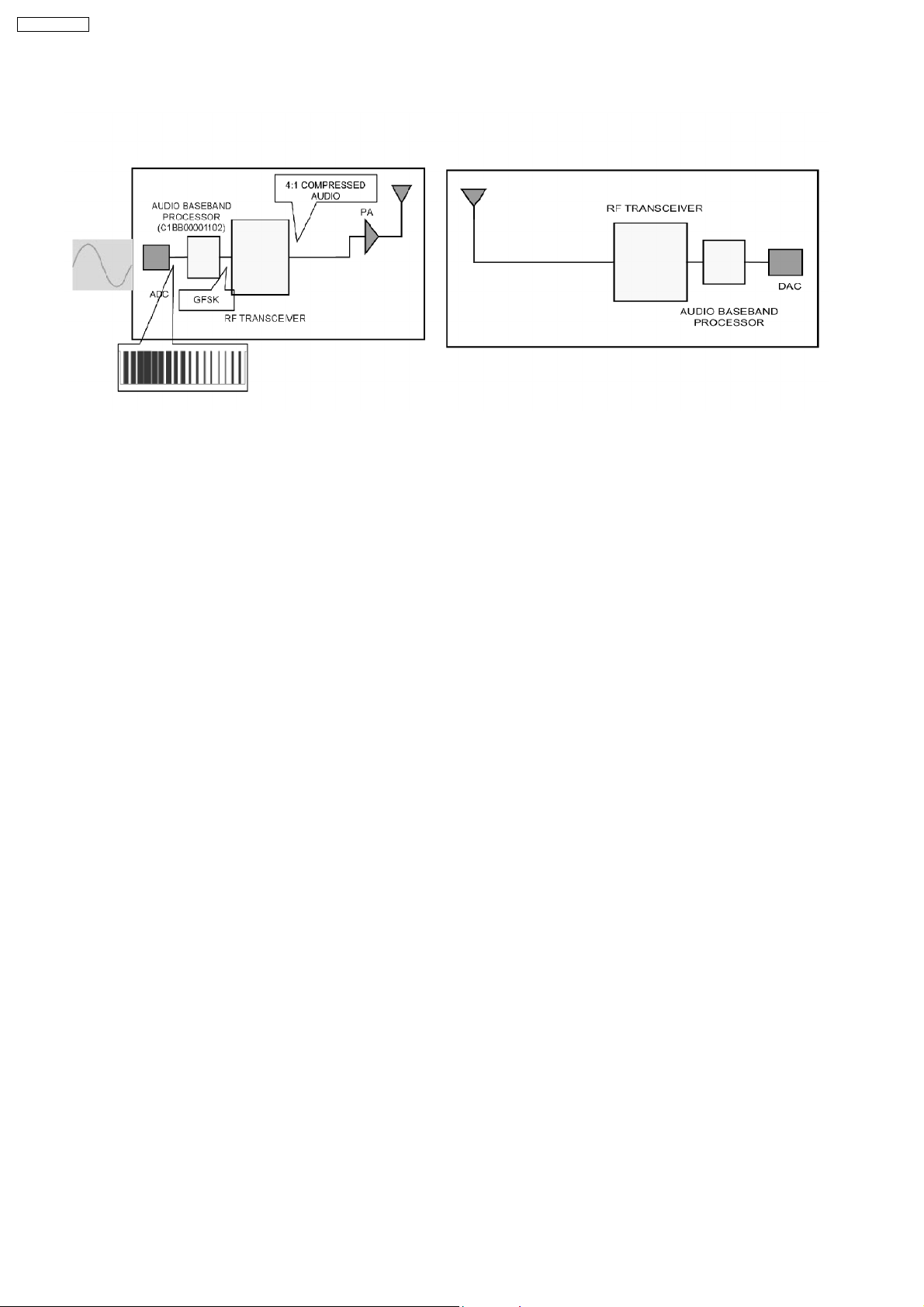
6.1. RF Wireless Audio Transceiver
6.1.1. Block Diagram
6.1.2. Definition
1. ADC : Analog-to-Digital Converter
2. Transceiver : Transmitter-Receiver Device
3. PA : Power Amplifier
4. DAC : Digital-to-Analog Converter
6.1.3. Features
· Crystal Clear CD Quality Stereo Sound
· Highly Robust Forward Error Correction
· 44.1KHz / 48KHz sampling frequency
· Adaptive Frequency Hopping System
· Range (open space) : 100m
· Low power consumption
· SNR (for left / right channel analog interface) : 80 dB
· THD : 0.2%
· Compact : 40mm x 80mm
10

6.2. Detail Block Diagram (Receiver module)
SH-HT995WGN
11
SH-HT995WGN
6.2.1. Operation
RF signal transmission and reception:
During the receive process, the radio signal is taken from a pair of balanc ed RF I/O pins that feed into the low noise amplifier (LNA).
Direct I/Q down conversion and on-chip filtering send the processed I/Q data to the analog-to-digital converter before processing
by the GFSK (Gaussian Frequency Shift Keying) demodulator. Within the demodulator, data detection and timing recovery circuits
convert the data for transfer to an external device. The transmit process operates in a similar fashion in reverse order.
The transmitted signal is GFSK (Gaussian Frequency Shift Keying) modulated data that is amplified on the chip to yield a radiated
output of 0dBm. A power control signal for an external amplifier is provided.
The audio baseband processor (C1BB00001102) is a digital audio processor IC encompassing apt-XTM audio
compress/decompress algorithm for wireless transmission of crystal-clear CD quality audio data.
For digital transmission the analog audio signals are sampled at 48kHz and converted to 1.536Mbps digital data through an
external 16-bit stereo audio codec. The digitized data are apt-XTM 4:1 compressed to 384Kbps stream data for efficient
transmission. Redundancy bits for forward error correction (FEC), synchronization flags, and control signals for time-division
duplexing (TDD) are appended to form data frames for error-free transmission.
In the receiver(Slave), synchronization flags and control data are first detected from the input stream. FEC decoder corrects any
errors that may have been introduced during the transmission and produces error-free compressed audio data. The compressed
audio is decompressed into 16-bit stereo PCM audio data through digital signal processing blocks. External audio codec converts
the PCM data to 2-channel (left and right) analog audio signals.
The Tx/Rx controller is in charge of several functions such as radio channel setup, frequency hopping for interference reduction and
generation of control signal for TDD and external RF chip.
In audio mode, the transmitter(Master) can send additional 16Kbps digital data simultaneously with stereo audio data.
How much time delay to transmit audio in wireless?
Audio compression and decompression requires about 3ms. Total time delay can be calculated as follows: Total delay time = audio
compression time + transmitter operating time + receiver operating time + audio decompression time. Total delay time is
approximately 12.2ms.
What is the power consumption?
The 2.4GHz RF module consumes about 45mA (max 65mA) for the transmitter and 55mA (max 71mA) for the receiver. The
EEPROM consumes about 1mA while the baseband IC consumes about 20mA.The total power consumption is 66mA (max 86mA)
for the transmitter and 76mA (max 92mA) for the receiver.
How does the system handle interference from other 2.4GHz RF devices?
12
SH-HT995WGN
It adopts Adaptive Frequency Hopping Spread Spectrum (AHSS) technology to avoid interference.
How does the system handle interference from other 2.4GHz RF devices?
The system supports 3 types of Spread Spectrum. These are
1. FHSS - Frequency Hopping Spread Spectrum
2. AHSS - Adaptive Frequency Hopping Spread Spectrum
3. Fixed Chann el Mode
FHSS refers to the conventional 79 channels (or 23 dependent on the country) hopping of Bluetooth. Devices using such hopping
method receives a lot of interference from other devices that use 2.4GHz range frequency such as WLAN and other Bluetooth
devices. FHSS, being built to avoid interfering with other devices, rather interferes a lot with devices that has high output power
using 2.4GHz frequency range and with other FHSS devices.During initialization, system scans 79 channe ls (or 23) and selects the
clear, non-interfered and reliable channel and starts the communication between master and slave. During the channel link, the
channel becomes unreliable and the error detection from FEC block exceeds the preset error threshold value, the system executes
scanning, as in initialization, and reselects new clear and reliable channel.
FHSS and AHSS can be selected by setting appropriate parameters on the EEPROM IC.
In Fixed Channel mode, 4 frequency levels can be selected (2.410GHz, 2.430G Hz, 2.450GHz and 2.470GHz)
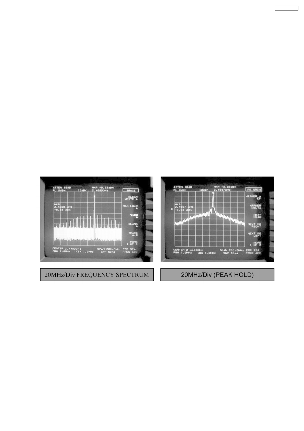
Spectrum distribution characteristic of 2.4GHz RF signal
13
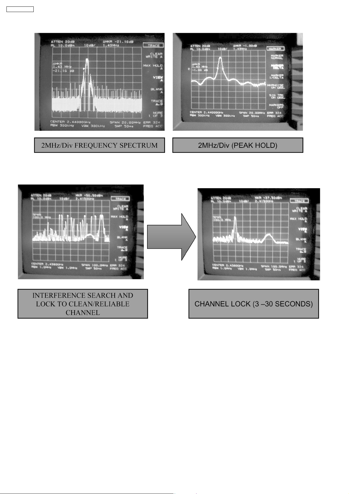
SH-HT995WGN
Spectrum distribution characteristic of 2.4GHz RF signal
How can Master or Slave setting be selected? By software or hardware?
It can be selected by external control pin.
How long does it take to transmit single packet?
To establish communication channel properly, hopping frequency and Syncword of each packet should be determined by Device
ID(Identification). Device ID is unique value of each device, master and slaves. Only master and slaves with same Device ID can
communicate each other. Device ID can be set manually in case selected master and slaves do not communicate together. This
procedure is *Device ID set*. Device ID set procedure occurs when master and slave devices boot simultaneously with ID_SET=1.
In this procedure, the slave can figure out the Device ID of the master and store it in external EEPROM.When ID_SET is
established, S5G3000 performs ID send/scan to send Device ID of master to slave before general page operation. In normal mode,
communication is accomplished by going into page state directly without ID send/scan.
How can the Master and Slave units be paired to prevent mix-up?
It takes 2.5ms.
14

SH-HT995WGN
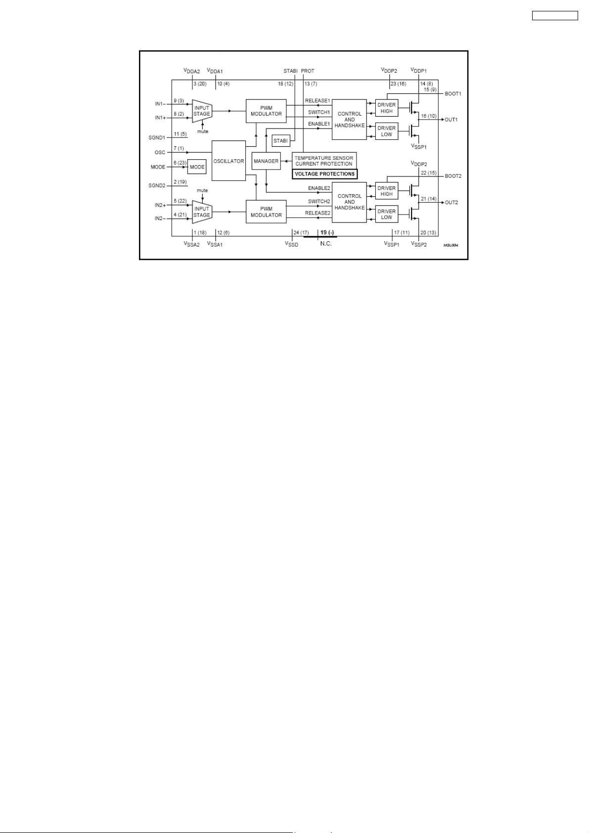
6.3. Class-D Amplifier
6.3.1. How are digital amplifiers different?
A digital amplifier incorporates a switching output stage that operates according to a principle known as pulse width modulation
(PWM). In contrast to the low-frequency control signal used in a conventional analog amplifier output stage, the switching output
stage of a digital amplifier is controlled by a high-frequency digital signal. The high-frequency digital signal is a PWM signal, in
which the music is modulated into a fixed-frequency carrier signal. In a digital amplifier, the modulation process is based on a digital
pulse code modula ted (PCM) representation of the music signal (or other signal that needs amplification) from a CD player, a DVD
player, or some other device.
BLOCK DIAGRAM OF TYPICAL ANALOG INPUT CLASS-D AMPLIFIER
6.3.2. What are the advantages of digital amplification technology?
· High power efficiency, i.e., smaller heat sinks and/or no fan required
· Compact (reduced PCB area)
· Low weight (reduced transformer size)
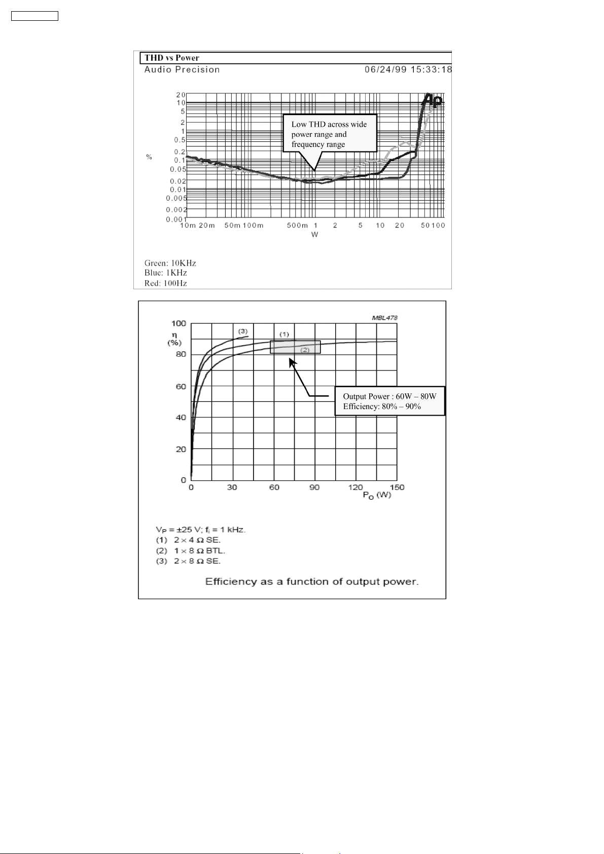
· Good sound quality (low signal distortion/THD)
6.3.3. Why is the digital amplifier so efficient?
A class-D amplifier is one in which the output transistors are operated as switches. When a transistor is off, the current through it
is zero. When it is on, the voltage across it is small, ideally zero. In each case, the power dissipation is very low.
6.3.4. Does the “D” in class-D mean DIGITAL?
No. This is not correct because the operation of the class-D amplifier is based on analog principles. There is no digital coding of
the signal. Before the advent of the class-D amplifier, the standard classes were class-A, class-AB, class-B, and class-C. The “D”
is simply the next letter in the alphabet after “C.” Indeed, the earliest work on class-D amplifiers involved vacuum tubes and can
be traced to the early 1950s.
15
SH-HT995WGN
6.3.5. Actual Class-D amplifier IC information
Part number: C1AA00000755 (TDA8920BJ)
Block diagram:
16
SH-HT995WGN
Soldering Information
If the temperature of the soldering iron bit is less than 300 °C it may remain in contact for up to 10 seconds. If the bit temperature
is between 300 and 400 °C, contact may be up to 5 seconds.
17

SH-HT995WGN
7 Assembling and Disassembling
7.1. Note
“ATTENTION SERVICER”
Some chassis components may be have sharp edges. Be careful when disassembling and servicing.
1. This section describes procedures for checking the operation of the major printed circuit boards and replacing the main
components.
2. For reassembly after operation checks or replacement, reverse the respective procedures.
Special reassembly procedures are described only when required.
3. Select items from the following index when checks or replacement are required.
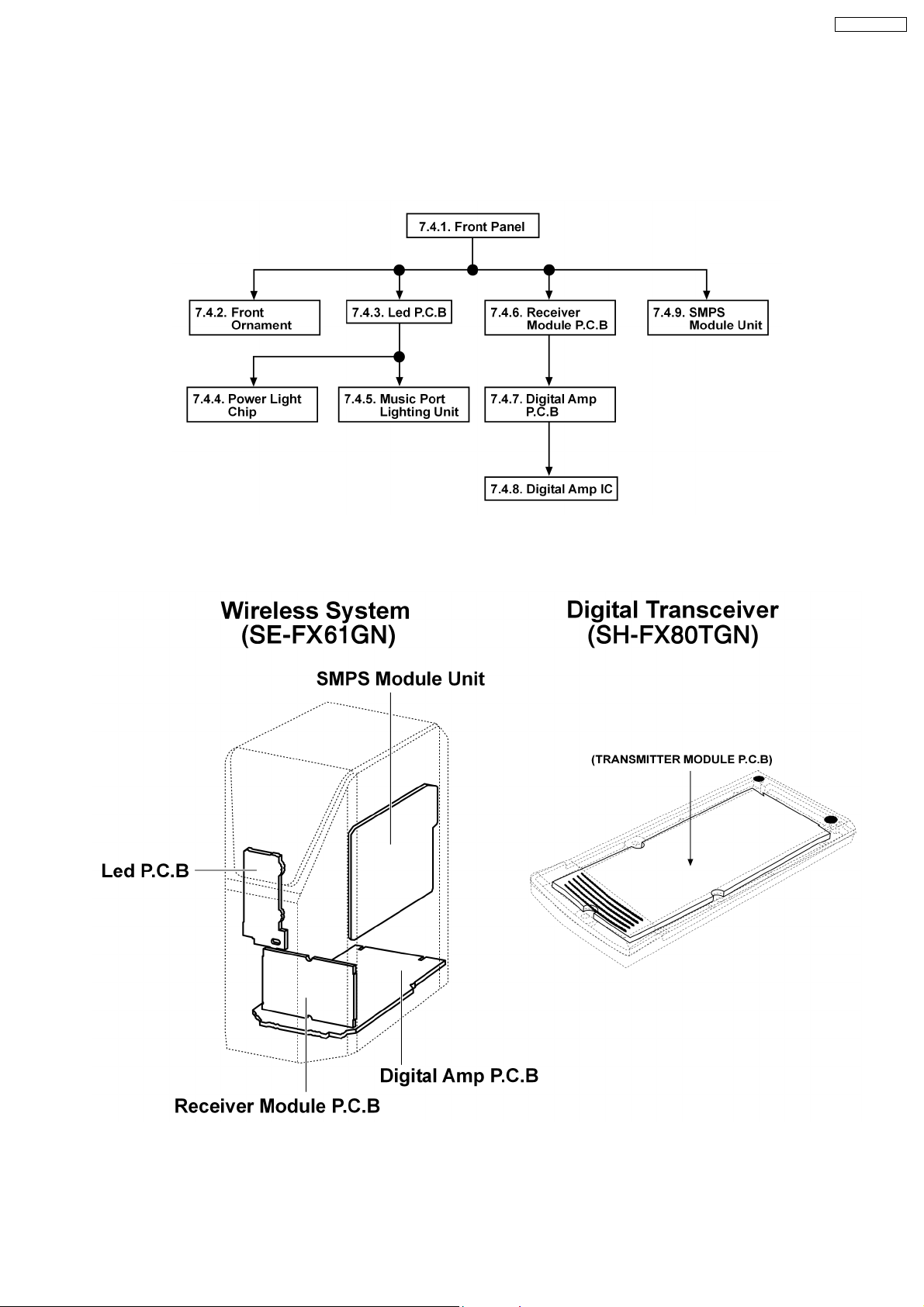
Below is the list of disassembly sections
· Disasse mbly of Front Panel
· Disasse mbly of Front Ornament
· Disasse mbly of Led P.C.B
· Disasse mbly of Power Light Chip
· Disasse mbly of Music Port Lighting Unit
· Disasse mbly of Receiver Module P.C.B
· Disasse mbly of Digital Amp P.C.B
· Disasse mbly of Digital Amp IC
· Disasse mbly of SMPS Module Unit
· Disasse mbly of Digital Transceiver (SH-FX80TGN)
7.1.1. SMPS Module Unit Replacement
1. This model uses SMPS Module unit to provide the necessary supply voltages for the receiver unit (SE-FX61).
2. It is advisable to replace the SMPS Module Unit if upon detecting of non-working conditions. Do not attempt to repair or replace
its components on board.
3. Non-working conditions include :
· No output voltage (±30V, ±5V) at pin 2,3,7,8,9, of H1000/W1 respectively.
· Broken fuse part (compatible substitute fuse part : K5D31 2BNA005).
18
SH-HT995WGN
7.2. Disassembly flow chart (For SE-FX61GN)
The following chart is the procedure for disassembling the casing and inside parts for internal inspection when carrying out the
servicing. For the digital receiver unit only.
To assemble the unit, reverse the steps shown in the chart below.
7.3. Main Parts Location Diagram
19
SH-HT995WGN
7.4. Disassembly of Wireless
System (SE-FX61GN)
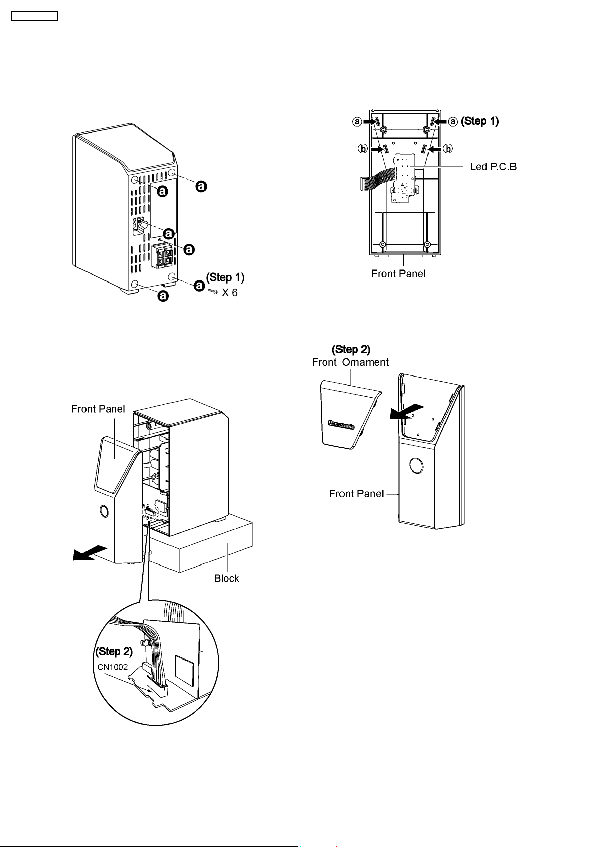
7.4.1. Disassembly of Front Panel
Step 1 : Remove 6 screws.
7.4.2. Disassembly of Front Ornament
· Follow the (Step 1) - (Step 3) of item 7.4.1.
Step 1 : Detach the catches as arrow shown.
Step 2 : Detach flat cable (CN1002).
Step 3 : Remove front panel.
Step 2 : Remove front ornament as arrow shown.
7.4.3. Disassembly of Led P.C.B
· Follow the (Step 1) - (Step 3) of item 7.4.1.
20
 Loading...