

Page 1
Wireless System and Digital Transceiver
Specification
n AMPLIFIER SECTION
RMS output power stereo mode
Surround Ch (both ch driven) 65 W per channel (4Ω), 1 kHz, 10
%THD
Total RMS stereo mode power 130 W
FTC output power stereo mode
Surround Ch (both ch driven) 40 W per channel (4Ω), 20 Hz-20
kHz, 1 % THD
Total FTC stereo mode power 80 W
n RF SECTION
Wireless module
Frequency range 2.402 to 2.480 GHz
RF output power 19 dBm (Max)
RF output impedance 50 Ω
Music Port (Rear)
Sensitivity 100 mV
Input impedance 4.7 kΩ
Terminal Stereo, 3.5 mm (1/8”) jack
ORDER NO. MD0607248CE
A6
SH-HT441WP
SH-FX60TPP
SE-FX60P
Colour
(S)..........Silver Type (For SH-HT441WP & SH-
FX60TPP only)
(S1)..........Silver Type (For SE-FX60P only)
Digital transceiver (SH-FX60TPP) 0.03 kg (0.07 lbs)
Wireless system (SE-FX60P) 0.7kg(1.5lbs)
Operating temperature range +5°Cto+35°C(+41°Fto+
95°F)
Operating humidity range 5 % to 90 % RH (no condensation)
Power consumption in standby mode
Transmit mode (SH-FX60TPP) 0.5 W
Receive mode (SE-FX60P) 1.2 W
n System : SC-HT441WP-S
Music Center : SA-HT441W P-S
Front Speaker : SB-FS440P-S
Surround Speaker : SB-FS441P-S
Center Speaker : SB-PC640P-S
Subwoofer : SB-W 440P-S
Digital Tx & Rx System : SH-
HT441W P-S
n GENERAL
Power supply AC 120 V, 60Hz
Power consumption
Digital transceiver (SH-FX60TPP) 0.85 W
Wireless system (SE-FX60P) 30 W
Dimensions (W x H x D)
Digital transceiver (SH-FX60TPP) 97 mm x 47.5 mm x 8.5 mm
(3-13/16” x 1-7/8” x 11/32”)
Wireless system (SE-FX60P) 89 mm x 189 mm x 180 mm
(3-1/2” x 7-7/16” x 7-3/32”)
Mass
© 2006 Matsushita Electric Industrial Co. Ltd.. All
rights reserved. Unauthorized copying and
distribution is a violation of law.
Page 2
SH-HT441WP
Power supply:
Notes:
1. Specifications are subject to change without notice.
Mass and dimensions are approximate
2. Total harmonic distortion is measured by a digital spectrum
analyzer
This model uses Switching Mode Power Supply (SMPS) Module for
powering the receiver unit. It is replaceable as an assembly unit.
CONTENTS
Page Page
1 Safety Precautions
1.1. GENERAL GUIDELINES
1.2. Before Repair and Adjustment (Digital Receiver SE-
FX60P)
1.3. Protection Circuitry
1.4. Caution for fuse replacement
2 Prevention of Electro Static Discharge (ESD) to
Electrostatically Sensitive (ES) Devices
3 Service caution based on legal restrictions
3.1. General description about Lead Free Solder (PbF)
4 Accessories
5 Using of Digital Receiver Unit
5.1. Connecting the digital transceiver (SH-FX60TPP)
5.2. Connecting the surround speaker cables to the wireless
system (SE-FX60P)
5.3. AC Power Cord connection (SE-FX60P)
5.4. Making the wireless link (SE-FX60P)
6 Technical Information (Wireless Surround)
6.1. RF Wireless Audio Transceiver
6.2. Detail Block Diagram (Receiver module)
6.3. Class-D Amplifier
7 Assembling and Disassembling
7.1. Note
7.2. Disassembly flow chart (For SE-FX60P)
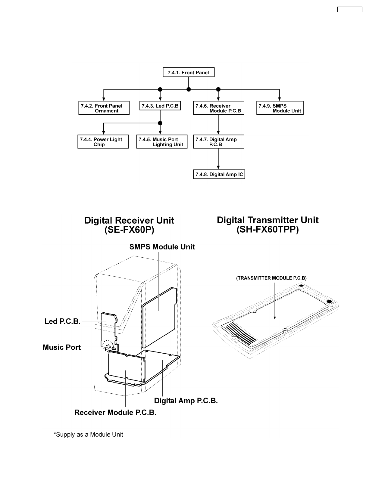
7.3. Main Parts Location Diagram
7.4. Disassembly of Wireless System (SE-FX60P)
7.5. Disassembly of Digital Transceiver (SH-FX60TPP)
8 Service Positions
8.1. Checking of Led and Receiver Module P.C.B.
8.2. Checking of Digital Amp and SMPS Module Unit
9 Service Hint
9.1. Use of Service Jig (RFKZFX50PP-S)
9.2. Procedures for testing of link between digital transmitter &
receiver
3
3
3
4
4
5
6
6
7
8
8
8
8
9
10
10
11
15
18
18
19
19
20
25
28
28
29
30
30
31
9.3. Troubleshooting Guide for Wireless Surround Speaker 33
10 Service parts replacement
10.1. Replacement of P.C.B.
10.2. Replacement of Transmitter Assembly
10.3. ID Location
10.4. Digital Transceiver Card Service Assembly
(RFKVHT441WPS)
11 Voltage Measurement
11.1. DIGITAL AMP P.C.B.
11.2. LED P.C.B.
12 Wiring Connection Diagram
13 Block Diagram
13.1. DIGITAL AMP MODULE BLOCK
13.2. RECEIVER MODULE BLOCK
13.3. TRANSIMITTER MODULE BLOCK
14 Notes of Schematic Diagram
15 Schematic Diagram
15.1. DIGITAL AMP CIRCUIT and LED CIRCUIT
15.2. RECEIVER MODULE CIRCUIT
15.3. TRANSMITTER MODULE CIRCUIT
16 Printed Circuit Board Diagram
16.1. DIGITAL AMP P.C.B and LED P.C.B
16.2. RECEIVER MODULE P.C.B and TRANSMITTER
MODULE P.C.B
17 Illustration of IC's, Transistors and Diodes
18 Terminal Functions of Integrated Circuits
18.1. IC12 (M9Z000000013): IC RF
19 Exploded Views
19.1. Cabinet Parts Location
19.2. Packaging
19.3. Main Unit Packaging
20 Replacement Parts List
20.1. Parts List (SE-FX60P)
20.2. Parts List (SH-FX60TPP)
35
35
35
36
37
38
38
38
39
41
41
42
43
45
47
47
48
50
53
53
54
55
56
56
57
57
58
59
60
60
63
2
Page 3

SH-HT441WP
1 Safety Precautions
1.1. GENERAL GUIDELINES
1. When servicing, observe the original lead dress. If a short circuit is found, replace all parts which have been overheated or
damaged by the short circuit.
2. After servicing, see to it that all the protective devices such as insulation barriers, insulation papers shields are properly
installed.
3. After servicing, make the following leakage current checks to prevent the customer from being exposed to shock hazards.
(This “Safety Precaution” is applied only in U.S.A.)
1. Before servicing, unplug the power cord to prevent an electric shock.
2. When replacing parts, use only manufacturer’s recommended components for safety.
3. Check the condition of the power cord. Replace if wear or damage is evident.
4. After servicing, be sure to restore the lead dress, insulation barriers, insulation papers, shields, etc.
5. Before returning the serviced equipment to the customer, be sure to make the following insulation resistance test to prevent the
customer from being exposed to a shock hazard.
1.1.1. LEAKAGE CURRENT COLD CHECK
1. Unplug the AC cord and connect a jumper between the two prongs on the plug.
2. Measure the resistance value, with an ohmmeter, between the jumpered AC plug and each exposed metallic cabinet part on
the equipment such as screwheads, connectors, control shafts, etc. When the exposed metallic part has a return path to the
chassis, the reading should be between 1MΩ and 5.2Ω.
When the exposed metal does not have a return path to the chassis, the reading must be
.
Figure. 1
1.1.2. LEAKAGE CURRENT HOT CHECK (See Figure 1.)
1. Plug the AC cord directly into the AC outlet. Do not use an isolation transformer for this check.
2. Connect a 1.5kΩ, 10 watts resistor, in parallel with a 0.15µF capacitors, between each exposed metallic part on the set and a
good earth ground such as a water pipe, as shown in Figure 1.
3. Use an AC voltmeter, with 1000 ohms/volt or more sensitivity, to measure the potential across the resistor.
4. Check each exposed metallic part, and measure the voltage at each point.
5. Reverse the AC plug in the AC outlet and repeat each of the above measurements.
6. The potential at any point should not exceed 0.75 volts RMS. A leakage current tester (Simpson Model 229 or equivalent) may
be used to make the hot checks, leakage current must not exceed 1/2 milliamp. In case a measurement is outside of the limits
specified, there is a possibility of a shock hazard, and the equipment should be repaired and rechecked before it is returned to
the customer.
1.2. Before Repair and Adjustment (Digital Receiver SE-FX60P)
This model uses switching mode power supply (SMPS) module to provide the necessary voltages for the receiver (SE-FX60P)
DO NOT SHORT-CIRCUIT DIRECTLY (with a screwdriver blade, for instance), as this may destroy solid state devices.
After repairs are completed, restore power gradually using a variac, to avoid overcurrent.
Current consum ption at AC 120V, 60Hz in NO SIGNAL mode (at volume minimum) should be ~150 mA.
3
Page 4
SH-HT441WP
1.3. Protection Circuitry
The protection circuitry may have operated if either of the following conditions are noticed:
· No sound is heard when the power is turned on.
· Stops during a performance.
The function of this circuitry is to prevent circuitry damage if, for example, the positive and negative speaker connection wires are
“shorted”, or if speaker systems with an impedance less than the indicated rated impedance of the amplifier are used.
If this occurs, follow the procedure outline s below:
1. Turn off the power.
2. Determine the cause of the problem and correct it.
3. Turn on the power once again after one minute.
Note:
When the protection circuitry functions, the unit will not operate unless the power is first turned off and then on again.
1.4. Caution for fuse replacement
Substituted service part no. for fuse: K5D312BNA005
4
Page 5
SH-HT441WP
2 Prevention of Electro Static Discharge (ESD) to
Electrostatically Sensitive (ES) Devices
Some semiconductor (solid state) devices can be damaged easily by electricity. Such components commonly are called
Electrostatically Sensitive (ES) Devices. Examples of typical ES devices are integrated circuits and some field-effect transistors and
semiconductor “chip” components. The following techniques should be used to help reduce the incidence of component damage
caused by electro static discharge (ESD).
1. Immediately before handling any semiconductor component or semiconductor-equiped assembly, drain off any ESD on your
body by touching a known earth ground. Alternatively, obtain and wear a commercially available discharging ESD wrist strap,
which should be removed for potent ial shock reasons prior to applyin g power to the unit under test.
2. After removing an electrical assembly equiped with ES devices, place the assembly on a conductive surface such as aluminium
foil, to prevent electrostatic charge build up or exposu re of the assembly.
3. Use only a grounded-tip soldering iron to solder or unsold er ES devices.
4. Use only an anti-static solder removal device. Some solder removal devices not classified as “anti-static (ESD protected)” can
generate electrical charge to damage ES devices.
5. Do not use freon-propelled chemicals. These can generate electrical charges sufficient to damage ES devices.
6. Do not remove a replacement ES device from its protective package until immediately before you are ready to install it. (Most
replacement ES devices are packaged with leads electrically shorted together by conductive foam, aluminium foil or
comparable conductive material).
7. Immediately before removing the protective material from the leads of a replacement ES device, touch the protective material
to the chassis or circuit assembly into which the device will be installe d.
Caution
Be sure no power is applied to the chassis or circuit, and observe all other safety precautions.
8. Minimize bodily motions when handling unpackaged replacement ES devices. (Otherwise harmless motion such as the
brushing together of your clothes fabric or the lifting of your foot from a carpeted floor can generate static electricity (ESD)
sufficient to damage an ES device).
5
Page 6
SH-HT441WP
3 Service caution based on legal restrictions
3.1. General description about Lead Free Solder (PbF)
The lead free solder has been used in the mounting process of all electrical components on the printed circuit boards used for this
equipment in considering the globally environmental conservation.
The normal solder is the alloy of tin (Sn) and lead (Pb). On the other hand, the lead free solder is the alloy mainly consists of tin
(Sn), silver (Ag) and Copper (Cu), and the melting point of the lead free solder is higher approx.30 degrees C (86°F) more than that
of the normal solder.
Definition of PCB Lead Free Solder being used
The letter of “PbF” is printed either foil side or components side on the PCB using the lead free solder.
(See right figure)
Service caution for repair work using Lead Free Solder (PbF)
· The lead free solder has to be used when repairing the equipment for which the lead free solder is used.
(Definition: The letter of “PbF” is printed on the PCB using the lead free solder.)
· To put lead free solder, it should be well molten and mixed with the original lead free solder.
· Remove the remaining lead free solder on the PCB cleanly for soldering of the new IC.
· Since the melting point of the lead free solder is higher than that of the normal lead solder, it takes the longer time to melt
the lead free solder.
· Use the soldering iron (more than 70W) equipped with the temperature control after setting the temperature at 350±30
degrees C (662±86°F).
Recommended Lead Free Solder (Service Parts Route.)
· The following 3 types of lead free solder are available through the service parts route.
RFKZ03D01K-----------(0.3mm 100g Reel)
RFKZ06D01K-----------(0.6mm 100g Reel)
RFKZ10D01K-----------(1.0mm 100g Reel)
Note
* Ingredient: Tin (Sn), 96.5%, Silver (Ag) 3.0%, Copper (Cu) 0.5%, Cobalt (Co) / Germanium (Ge) 0.1 to 0.3%
6
Page 7

4 Accessories
Note : Refer to Packing Materials & Accessories Parts List (Section 20) for the part number.
AC Power Cord
SH-HT441WP
7
Page 8
SH-HT441WP
5 Using of Digital Receiver Unit
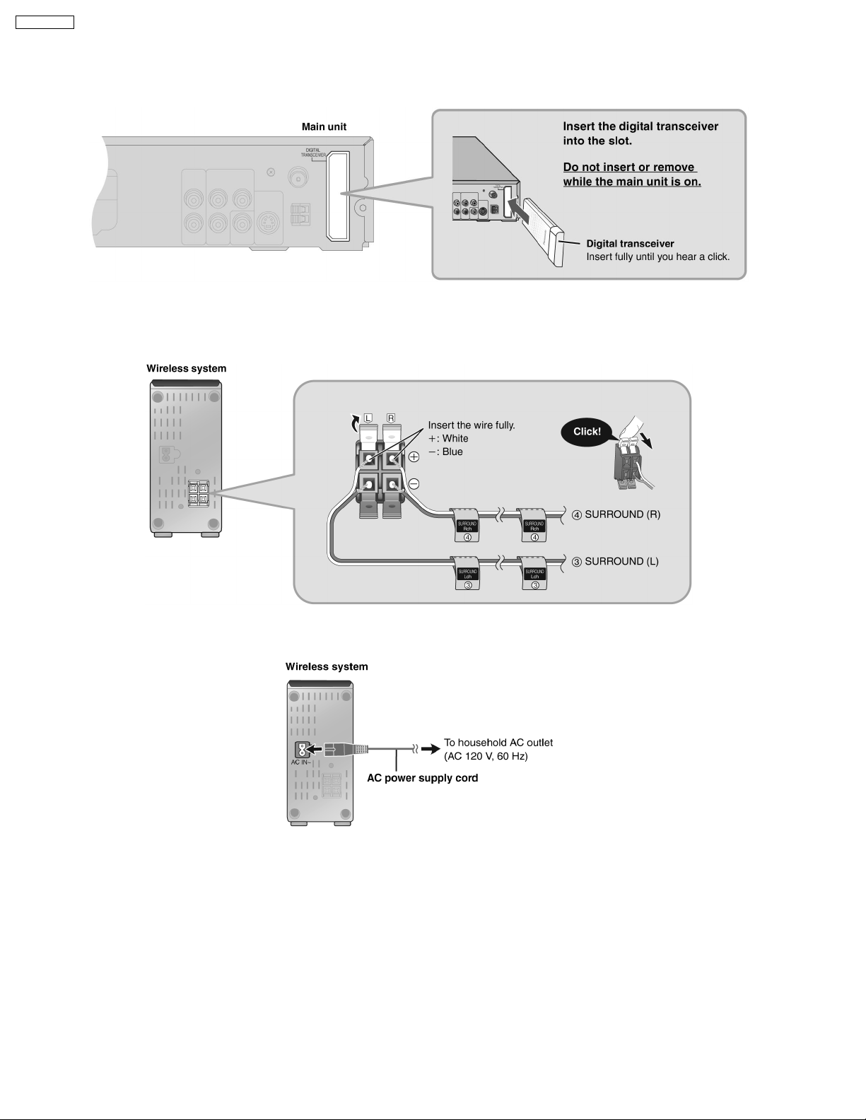
5.1. Connecting the digital transceiver (SH-FX60TPP)
5.2. Connecting the surround speaker cables to the wireless system (SEFX60P)
5.3. AC Power Cord connection (SE-FX60P)
8
Page 9

5.4. Making the wireless link (SE-FX60P)
SH-HT441WP
9
Page 10
SH-HT441WP
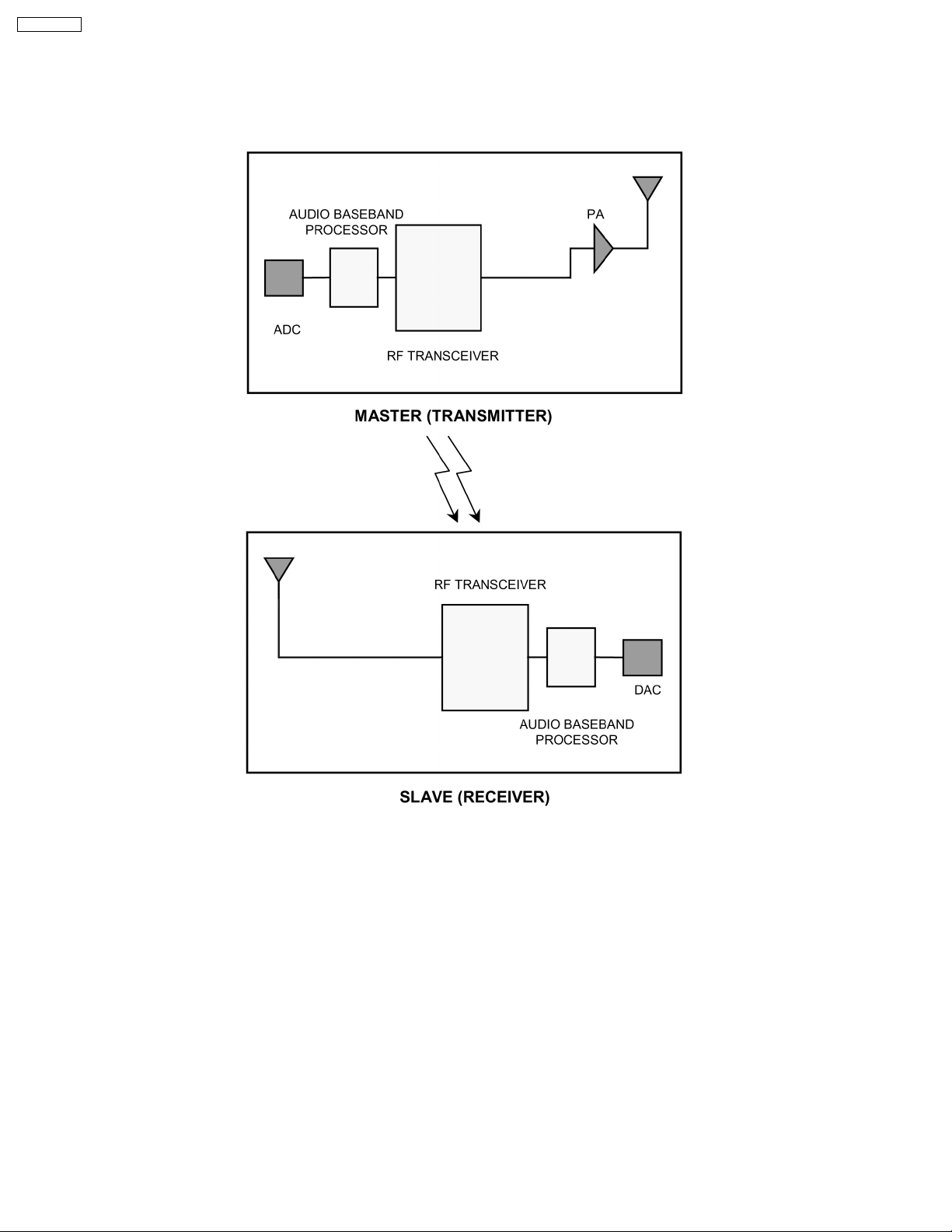
6 Technical Information (Wireless Surround)
6.1. RF Wireless Audio Transceiver
6.1.1. Block Diagram
6.1.2. Definition
1. ADC : Analog -to-Digital Converter
2. Transceiver : Transmitter-Receiver Device
3. PA : Power Amplifier
4. DAC : Digital-to-Analog Converter
6.1.3. Features
· Crystal Clear CD Quality Stereo Sound
· Highly Robust Forward Error Correction
· 44.1KHz / 48KHz sampling frequency
· Adaptive Frequency Hoppin g System
· Range (open space) : 100m
· Low power consum ption
· SNR (for left / right channel analog interface) : 80 dB
· THD : 0.2%
· Compact : 40mm x 80mm
10
Page 11
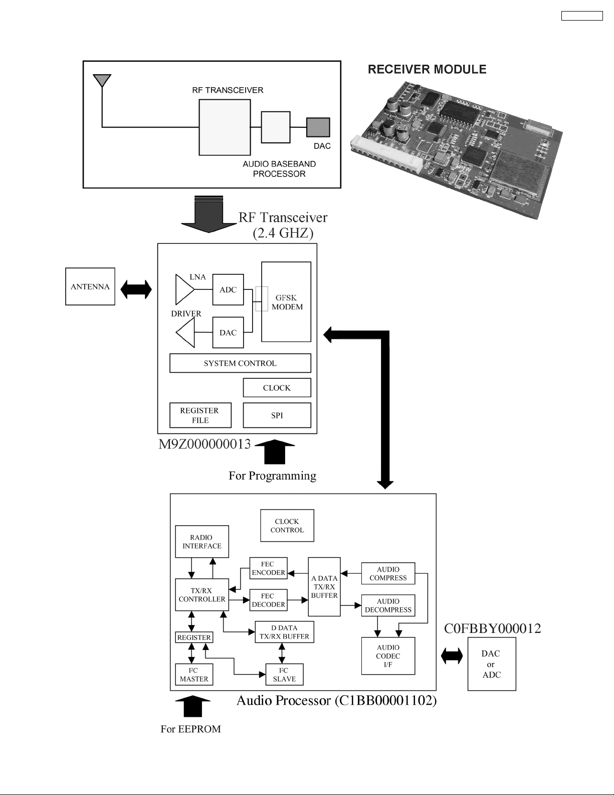
6.2. Detail Block Diagram (Receiver module)
SH-HT441WP
11
Page 12

SH-HT441WP
6.2.1. Operation
RF signal transmission and reception:
During the receive process, the radio signal is taken from a pair of balanc ed RF I/O pins that feed into the low noise amplifier (LNA).
Direct I/Q down conversion and on-chip filtering send the processed I/Q data to the analog-to-digital converter before processing
by the GFSK (Gaussian Frequency Shift Keying) demodulator. Within the demodulator, data detection and timing recovery circuits
convert the data for transfer to an external device. The transmit process operates in a similar fashion in reverse order.
The transmitted signal is GFSK (Gaussian Frequency Shift Keying) modulated data that is amplified on the chip to yield a radiated
output of 0dBm. A power control signal for an external amplifier is provided.
The audio baseband processor (C1BB00001102) is a digital audio processor IC encompassing apt-XTM audio
compress/decompress algorithm for wireless transmission of crystal-clear CD quality audio data.
For digital transmission the analog audio signals are sampled at 48kHz and converted to 1.536Mbps digital data through an
external 16-bit stereo audio codec. The digitized data are apt-XTM 4:1 compressed to 384Kbps stream data for efficient
transmission. Redundancy bits for forward error correction (FEC), synchronization flags, and control signals for time-division
duplexing (TDD) are appended to form data frames for error-free transmission.
In the receiver(Slave), synchronization flags and control data are first detected from the input stream. FEC decoder corrects any
errors that may have been introduced during the transmission and produces error-free compressed audio data. The compressed
audio is decompressed into 16-bit stereo PCM audio data through digital signal processing blocks. External audio codec converts
the PCM data to 2-channel (left and right) analog audio signals.
The Tx/Rx controller is in charge of several functions such as radio channel setup, frequency hopping for interference reduction and
generation of control signal for TDD and external RF chip.
In audio mode, the transmitter(Master) can send additional 16Kbps digital data simultaneously with stereo audio data.
How much time delay to transmit audio in wireless?
Audio compression and decompression requires about 3ms. Total time delay can be calculated as follows: Total delay time = audio
compression time + transmitter operating time + receiver operating time + audio decompression time. Total delay time is
approximately 12.2ms.
What is the power consumption?
The 2.4GHz RF module consumes about 45mA (max 65mA) for the transmitter and 55mA (max 71mA) for the receiver. The
EEPROM consumes about 1mA while the baseband IC consumes about 20mA.The total power consumption is 66mA (max 86mA)
for the transmitter and 76mA (max 92mA) for the receiver.
How does the system handle interference from other 2.4GHz RF devices?
12
Page 13
SH-HT441WP
It adopts Adaptive Frequency Hoppin g Spread Spectrum (AHSS) technology to avoid interference.
How does the system handle interference from other 2.4GHz RF devices?
The system supports 3 types of Spread Spectrum. These are
1. FHSS - Frequency Hopping Spread Spectrum
2. AHSS - Adaptive Frequency Hopping Spread Spectrum
3. Fixed Chann el Mode
FHSS refers to the conventional 79 channels (or 23 dependent on the country) hopping of Bluetooth. Devices using such hopping
method receives a lot of interference from other devices that use 2.4GHz range frequency such as WLAN and other Bluetooth
devices. FHSS, being built to avoid interfering with other devices, rather interferes a lot with devices that has high output power
using 2.4GHz frequency range and with other FHSS devices.During initialization, system scans 79 channels (or 23) and selects the
clear, non-interfered and reliable channel and starts the communication between master and slave. During the channel link, the
channel becomes unreliable and the error detection from FEC block exceeds the preset error threshold value, the system executes
scanning, as in initialization, and reselects new clear and reliable channel.
FHSS and AHSS can be selected by setting appropriate parameters on the EEPROM IC.
In Fixed Channel mode, 4 frequency levels can be selected (2.410GHz, 2.430GHz, 2.450GHz and 2.470GHz)
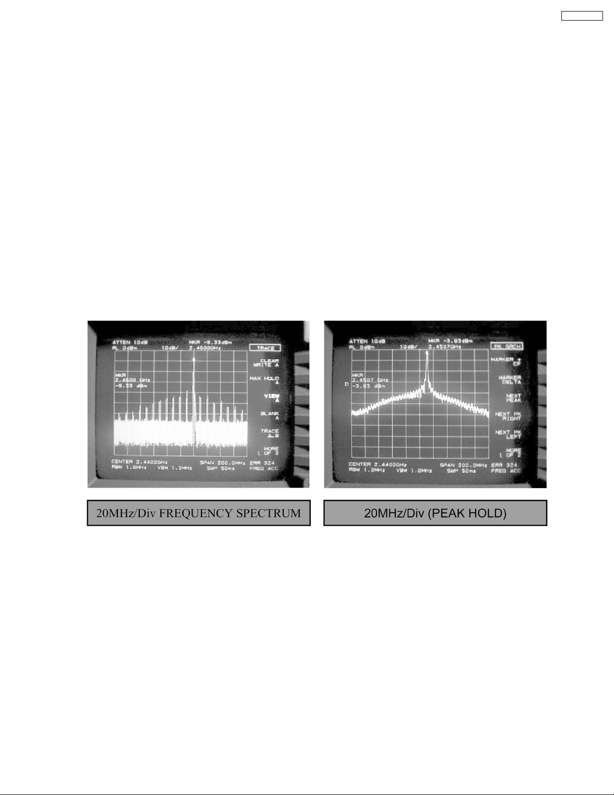
Spectrum distribution characteristic of 2.4GHz RF signal
13
Page 14

SH-HT441WP
Spectrum distribution characteristic of 2.4GHz RF signal
How can Master or Slave setting be selected? By software or hardware?
It can be selected by external control pin.
How long does it take to transmit single packet?
To establish communication channel properly, hopping frequency and Syncword of each packet should be determined by Device
ID(Identification). Device ID is unique value of each device, master and slaves. Only master and slaves with same Device ID can
communicate each other. Device ID can be set manually in case selected master and slaves do not communicate together. This
procedure is *Device ID set*. Device ID set procedure occurs when master and slave devices boot simultaneously with ID_SET=1.
In this procedure, the slave can figure out the Device ID of the master and store it in external EEPROM.When ID_SET is
established, S5G3000 performs ID send/scan to send Device ID of master to slave before general page operation. In normal mode,
communication is accomplished by going into page state directly without ID send/scan.
How can the Master and Slave units be paired to prevent mix-up?
It takes 2.5ms.
14
Page 15

SH-HT441WP
6.3. Class-D Amplifier
6.3.1. How are digital amplifiers different?
A digital amplifier incorporates a switching output stage that operates according to a principle known as pulse width modulation
(PWM). In contrast to the low-frequency control signal used in a conventional analog amplifier output stage, the switching output
stage of a digital amplifier is controlled by a high-frequency digital signal. The high-frequency digital signal is a PWM signal, in
which the music is modulated into a fixed-frequency carrier signal. In a digital amplifier, the modulation process is based on a digital
pulse code modula ted (PCM) representation of the music signal (or other signal that needs amplification) from a CD player, a DVD
player, or some other device.
BLOCK DIAGRAM OF TYPICAL ANALOG INPUT CLASS-D AMPLIFIER
6.3.2. What are the advantages of digital amplification technology?
· High power efficiency, i.e., smaller heat sinks and/or no fan required
· Compact (reduced PCB area)
· Low weight (reduced transformer size)
· Good sound quality (low signal distortion/THD)
6.3.3. Why is the digital amplifier so efficient?
A class-D amplifier is one in which the output transistors are operated as switches. When a transistor is off, the current through it
is zero. When it is on, the voltage across it is small, ideally zero. In each case, the power dissipation is very low.
6.3.4. Does the “D” in class-D mean DIGITAL?
No. This is not correct because the operation of the class-D amplifier is based on analog principles. There is no digital coding of
the signal. Before the advent of the class-D amplifier, the standard classes were class-A, class-AB, class-B, and class-C. The “D”
is simply the next letter in the alphabet after “C.” Indeed, the earliest work on class-D amplifiers involved vacuum tubes and can
be traced to the early 1950s.
15
Page 16
SH-HT441WP
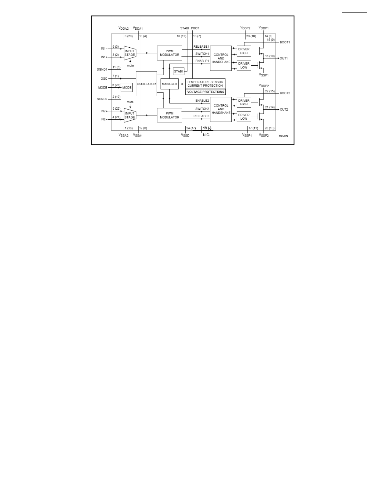
6.3.5. Actual Class-D amplifier IC information
Part number: C1AA0 0000755 (TDA8920BJ)
Block diagram:
16
Page 17
SH-HT441WP
Soldering Information
If the temperature of the soldering iron bit is less than 300 °C it may remain in contact for up to 10 seconds. If the bit temperature
is between 300 and 400 °C, contact may be up to 5 seconds.
17
Page 18

SH-HT441WP
7 Assembling and Disassembling
7.1. Note
“ATTENTION SERVICER”
Some chassis components may be have sharp edges. Be careful when disassembling and servicing.
1. This section describes procedures for checking the operation of the major printed circuit boards and replacing the main
components.
2. For reassembly after operation checks or replacement, reverse the respective procedures.
Special reassembly procedures are described only when required.
3. Select items from the following index when checks or replacement are required.
Below is the list of disassembly sections
· Disasse mbly of Front Panel
· Disasse mbly of Front Panel Ornament
· Disasse mbly of Led P.C.B
· Disasse mbly of Power Light Chip
· Disasse mbly of Music Port Lighting Unit
· Disasse mbly of Receiver Module P.C.B
· Disasse mbly of Digital Amp P.C.B
· Disasse mbly of Digital Amp IC
· Disasse mbly of SMPS Module Unit
· Disasse mbly of Digital Transceiver (SH-FX60TPP)
7.1.1. SMPS Module Unit Replacement
1. This model uses SMPS Module unit to provide the necessary supply voltages for the receiver unit (SE-FX60).
2. It is advisable to replace the SMPS Module Unit if upon detecting of non-working conditions. Do not attempt to repair or replace
its components on board.
3. Non-working conditions include:
· No output voltage (±30V, ±5V) at pin 2,3,7,8,9, of H1000/W1 respectively.
· Broken fuse part (compatible substitute fuse part : K5D312BNA005).
18
Page 19
SH-HT441WP
7.2. Disassembly flow chart (For SE-FX60P)
The following chart is the procedure for disassembling the casing and inside parts for internal inspection when carrying out the
servicing. For the digital receiver unit only.
To assemble the unit, reverse the steps shown in the chart below.
7.3. Main Parts Location Diagram
19
Page 20

SH-HT441WP
7.4. Disassembly of Wireless
System (SE-FX60P)
7.4.1. Disassembly of Front Panel
Step 1 : Remove 6 screws.
7.4.2. Disassembly of Front Panel
Ornament
· Follow the (Step 1) - (Step 3) of item 7.4.1.
Step 1 : Detach the catches as arrow shown.
Step 2 : Detach flat cable (CN1002).
Step 3 : Remove front panel.
Step 2 : Remove front panel ornament as arrow shown.
7.4.3. Disassembly of Led P.C.B
· Follow the (Step 1) - (Step 3) of item 7.4.1.
20
Page 21

Step 1 : Remove 3 screws.
SH-HT441WP
Step 1 : Detach power light chip from front panel assembly.
7.4.5. Disassembly of Music Port
Lighting Unit
· Follow the (Step 1) - (Step 3) of item 7.4.1.
· Follow the (Step 1) - (Step 2) of item 7.4.3.
Step 2 : Detach Led P.C.B from the front panel assembly.
7.4.4. Disassembly of Power Light Chip
· Follow the (Step 1) - (Step 3) of item 7.4.1.
· Follow the (Step 1) - (Step 2) of item 7.4.3.
Step 1 : Detach the catches of music port lighting unit from Led
P.C.B.
21
Page 22

SH-HT441WP
Step 2 : Remove music port lighting unit as arrow shown.
7.4.6. Disassembly of Receiver Module
P.C.B
· Follow the (Step 1) - (Step 3) of item 7.4.1.
Step 2 : Detach the flat cable from the ribs of back cabinet
assembly.
Step 3 : Detach connector CN1003 and remove Receiver
Module P.C.B.
Note: Ensure during assembly, the flat cable must be
properly dressed in between the 2 supporting ribs.
Step 1 : Push in the Speaker Jack (JK1002) as arrow shown.
Note: Take note of the 2 catches on the inside of the back
cabinet assembly.
When pushing up the Speak er Jack (JK1002), be careful
not to break the catches and do not apply too much
pressure on them.
22
Page 23

Step 4 : Desolder 4 points on the receiver shield plate as
shown.
SH-HT441WP
Step 6 : Desolder 4 points on the transmitter shield plate as
shown.
Step 5 : Detach Rx shield plate as arrow shown.
Step 7 : Detach transmitter shield plate as arrow shown.
7.4.7. Disassembly of Digital Amp P.C.B
· Follow the (Step 1) - (Step 3) of item 7.4.1.
· Follow the (Step 1) - (Step 2) of item 7.4.6.
23
Page 24

SH-HT441WP
Step 1 : Detach flat cable (CN2) .
Step 2 : Remove Digital Amp P.C.B as arrow shown.
Step 2 : De-solder and remove IC1500.
7.4.8. Disassembly of Digital Amp IC
· Follow the (Step 1) - (Step 3) of item 7.4.1.
· Follow the (Step 1) - (Step 2) of item 7.4.6.
· Follow the (Step 1) - (Step 2) of item 7.4.7.
Step 3 : Detach IC1500 from heat sink unit.
Step 1 : Remove heat sink clip as arrow shown.
Step 4 : Detach IC Insurator A from heat sink unit.
7.4.9. Disassembly of SMPS Module Unit
· Follow the (Step 1) - (Step 3) of item 7.4.1.
24
Page 25

Step 1 : Detach flat cable (CN2).
Step 2 : Remove SMPS Module as arrow shown.
SH-HT441WP
Step 2 : Remove bottom casing as arrow shown.
7.5. Disassembly of Digital
Transceiver (SH-FX60TPP)
Step 1 : Remove 4 screws.
Step 3 : Remove Transmitter Module P.C.B as arrow shown.
25
Page 26

SH-HT441WP
Step 4 : Desold er 4 points from Transmitter Module P.C.B.
Step 6 : Desold er 4 points from Transmitter Module P.C.B.
Step 5 : Remove Tx shield plate as arrow shown.
Step 7 : Remove Rx shield plate as arrow shown.
· Assembly of Digital Transceiver (SH-FX60TPP)
26
Page 27

Step 1 : Fix side-A ends of bottom casing and top casing
together.
Step 2 : Fit bottom casing and top casing together from side-A
to side-B.
SH-HT441WP
27
Page 28

SH-HT441WP
8 Service Positions
Note: For description of the disassembly procedures, see the Section 7.
8.1. Checking of Led and Receiver Module P.C.B.
28
Page 29

8.2. Checking of Digital Amp and SMPS Module Unit
SH-HT441WP
29
Page 30

SH-HT441WP
9 Service Hint
9.1. Use of Service Jig (RFKZFX50PP-S)
The service jig (Part No. RFKZFX50PP-S) is used for the purpose of testing the link between the digital transmitter and receiver
unit.It is available to see either the digital transmitter & receiver or Home Theater unit has cause of no connection to the
wirelesslink.
Below is the block diagram for the connection of the service jig:-
30
Page 31

SH-HT441WP
9.2. Procedures for testing of link between digital transmitter & receiver
Below is the list of steps to be carry out for the testing of the link between the digital transmitter & the receiver unit: -
Step 1 : Insert the digital transmitter unit into the service jig. (Part No. RFKZFX50PP-S)
Step 2 : Connect the 5V from the DC power source to the service jig as indicated by the jumper “5V”. Ensure that the DC power
source is connected properly.
Step 3 : Connect the Audio Signals (L & R) to the service jig as indicated by the jumpers (Left & Right) respectively from an audio
source.
Step 4 : Power on the digital Transmitter unit via the 5V DC power source.
Step 5 : Power on the digital receiver unit via AC power source by pressing the Power on/off button.
Ensure that the light indicator at the receiver unit is turn on. (Refer to the diagram below for the location of the Power on/off button)
31
Page 32

SH-HT441WP
Step 6 : Ensure that the Green LED (Digital Transmitter) is light-up. If it does not light up, there is no established link between them.
(No communication is established between the digital transmitter & receiver unit). It could be due the below possible causes:
1. The digital transmitter unit is not fully inserted into the slot of the service jig. (Note: The wireless link indicator light will be
flashing if the digital transmitter unit is not fully inserted into the slot.
2. The 5V DC power supply to the service jig is not connected properly or it is connected loosely.
3. The digital transmitter or the receiver unit is not operating properly due to power supply not connected properly. (Refer to
section 9.3.1 for troubleshooting procedures for the receiver module P.C.B.)
Step 7 : Ensure that the audio input into the digital transmitter can be heard from the speaker at the digital receiver unit. If there
is no audio output at the speaker, check and confirm the connection of speakers at the rear of the receiver unit. (Refer to section
9.3.3 for the troubleshooting procedures for checking of power Amp IC).
32
Page 33

9.3. Troubleshooting Guide for Wireless Surround Speaker
9.3.1. Troubleshooting for digital receiver unit (SE-FX60P)
Problem Phenomenon Possible Causes
No Audio Output (At surround
speaker)
1. No wireless connection between the main unit and
the digital receiver unit (SE-FX60).
1. Transmitter card is not inserted properly in
the main unit.
SH-HT441WP
Intermittent Audio output (At surround
speaker)
Note: When using Home Theater unit SU-RX57
The wireless option LED of the unit will not light up if
the wireless connection link is not established. If the
wireless option LED lights up, it means the wireless link
connection is established.
When using Home Theater unit SH-HT805W-S
FL Display on main unit will not show "W" if the wireless
connection link is not established. If FL displays shows
"W", it means the wireless link connection is
established.
Wireless link connection is established with FL display
showing "W"
2. No AC input power to the digital receiver
unit (SE-FX60) or AC cord faulty.
3. Shorted/Open circuit at speaker jack.
4. SMPS module unit or the digital amp P.C.B
is not working properly (For more
information, refer to section 9.2 on the
troubleshooting of the digital amp circuit.)
5. Transmitter card is not working properly due
to faulty parts within.
6. No +5V supply voltage to the transmitter
card due to failure within Home Theater
unit. (Refer to the troubleshooting for Home
Theater unit)
1. Transmitted signal interrupted by nearby
operating devices.
2. Loose speaker wire connection SMPS
module unit or the digital amp P.C.B is not
working properly (For more information,
refer to following section on the
troubleshooting of the digital amp circuit.)
Special Note: The digital transceiver and the receiver module P.C.B should be replaced using the transmitter assembly
(RFKVHFX60PPS) if it is found in not working condition.
9.3.2. Troubleshooting for digital amp circuit (Step By Step guide)
Below is the step by step guide on the troubleshooting of the digital amp circuit (When there is no audio output): -
Procedures Checking points Checking components
Step 1 Check open/short circuit connection at speaker jack JK1002, L1601-L1603 (Replace parts when
Step 2 1. Check regulated supply voltage +27V (pin 4, 8, 16
& 20)
2. Check regulated supply voltage -27V (pin 6, 11, 13
& 18)
Regulated supply to digital amp IC from SMPS module
unit.
determine NG)
Digital amp IC, IC1500
1. If no supply voltages to IC1500, go to Step
3.
2. If there is regulated voltage supply to
IC1500, go to Step 4.
33
Page 34

SH-HT441WP
Procedures Checking points Checking components
Step 3 Check for supply voltage +30V (pin 1 & 2) / -30V (pin 6
& 7) & +5V (pin 8)
Step 4 Check for supply voltage at pin 4 (+VCC) & 8 (-Vcc) Op-amp IC, IC1501If there is supply voltages to
Step 5 Check voltage regulator circuit Q1000, Q1002, Q1010 & Q1011If parts NG,
Step 6 1. Check for output audio signal at pin 10 & 14
2. Check for input audio signal at pin 3 & 22
No supply voltages (from SMPS module unit to
Digital amp P.C.B), check the following: -
1. Wire cable (W1) at H1000 (Digital amp
P.C.B)
2. F1 (blown fuse),
3. SMPS module unit (Faulty parts with burnt
mark etc)
4. AC Inlet Jack (SMPS module unit).
If there is supply from SMPS module unit, go to
Step 4
Special note: SMPS module should be replaced
if determined NG.
IC1501, proceed to Step 6If no supply voltages
to IC1501, proceed to Step 5
replaced.
Digital amp IC, IC1500
If there is input signal but no generated output
signal from IC1500 (all supply voltages is
present), replaced IC1500.
If there is no input audio signal, go to Step 7 for
checking on the Op-amp output.
Step 7 1. Check for output audio signal at pin 1 & 7
2. Check for input audio signal at pin 2 & 6
Step 8 Check input audio signal at pin 5 & 7 (CN1003) If no input signal, check following:
Step 9 (For music port input only) Check input signal at pin 6 & 8 (CN1002) If no input signal, check following:
Op-amp IC, IC1501
If there is input signal but no output signal from
IC1501, (all supply voltages is present),
replaced IC1501.
If there is no input signal, go to Step 8
1. FFC cable NG
2. FFC cable not connected properly
3. Receiver module P.C.B NG (parts NG Baseband IC, RF antenna etc)
4. No signal received by Receiver module due
to no transmission from the digital
transmitter.
5. No supply to receiver module. (Check pin 8
at H1000 from SMPS module)
1. If wire cable is not connected properly or
NG.
2. Music port jack abnormal (shorted).
(SMPS stands for switching mode power supply)
Special Note: The SMPS module unit is supplied as service parts and should be replaced as a unit if it is in not working condition.
34
Page 35

SH-HT441WP
10 Service parts replacement
10.1. Replacement of P.C.B.
Part No Part Name & Descriptions Applied models Remarks
RFKBHFX60PPS Module Kit Assembly SH-HT441WP-S [M]
Table 1
· Both Transmitter module P.C.B and Receiver Module P.C.B. should be replaced together using above Module Kit unit when you
find fault of IC5 within at the service operation.
· If ID codes of IC5 located on the back of both Transmitter and Receiver P.C.B. are not correspondent, wireless link will not be
established.
· The Module Kit unit is designed for the paired kit of the transmitter & receiver module P.C.B. with the same ID code.
10.2. Replacement of Transmitter Assembly
[In case of replacement of a new Transmitter by necessity, i.e, its loss.]
Applied models Digital system Transmitter Receiver
- SH-HT441WP-S SH-FX60TPPS SE-FX60P-S1
Table 2
· Both Transmitter Module P.C.B and Receiver Module P.C.B. should be replaced together using above Module Kit unit.
· If ID codes of IC5 located on the back of both Transmitter and Receiver P.C.B. are not correspondent, wireless link will not be
established as P.C.B.
· The Module Kit unit is designed for the paired kit of the transmitter & receiver module P.C.B. with the same ID code.
RFKVHFX60PPS Transmitter Assembly
Failure to do so may lead to the disabled of receiver unit due to ID codes mismatched hence no function of wireless surround.
35
Page 36

SH-HT441WP
10.3. ID Location
10.3.1. Transmitter Module P.C.B.
10.3.2. Receiver Module P.C.B.
36
Page 37

10.4. Digital Transceiver Card Service Assembly (RFKVHT441WPS)
If the digital transceiver card is lost, the Module kit assembly can be used for as service parts replacement.
The following steps needed to be performed together using main unit when replacing with new digital transceiver kit.
10.4.1. ID SET
1. Remove Back Cabinet Assembly.
2. Remove DAMP P.C.B & SMPS module unit.
3. Connect a wire to Pin 10 of Receiver Module P.C.B.
4. Power Up the digital receiver unit (SE-FX60).
5. Insert the transceiver into main unit.
6. Press “Surround Music” for main unit until the wireless LED lights up & FL displays “W”.
7. Short the wire on Receiver Module P.C.B to GROUND (Pin 2).
SH-HT441WP
37
Page 38

11 Voltage Measurement
Note:
· Indicated voltage values are the standard values for the unit measured by the DC electronic circuit tester (high-impedance)
with the chassis taken as standard.
Therefore, there may exist some errors in the voltage values, depending on the internal impedance of the DC circuit tester.
· Circuit voltage and waveform described herein shall be regarded as reference information when probing defect point
because it may differ from actual measuring value due to difference of Measuring instrument and its measuring condition
and product itself.
11.1. DIGITAL AMP P.C.B.
DIGITAL AMP P.C.B.
Ref No.
MODE 1 2 3 4 5 6 7 8 9 10 11 12 13 14 15 16 17 18 19 20
POWER ON -28.3 0 0 29.4 0 -28.3 -27..3 29.4 0 0 -28.4 -28.2 -28.3 -0.1 0 29.9 -28.4 -28.7 0 29.4
STANDBY -28.6 0 0 29.1 0 -28.7 -27.7 29.1 0 -0.6 -28.7 -28.5 -28.6 -27.5 -24.5 29.1 -28.7 -28.7 0 29.1
Ref No.
MODE 21 22 23
POWER ON 0 0 0
STANDBY 0 0 0
Ref No.
MODE 1 2 3 4 5 6 7 8
POWER ON 0 0 0 -0.3 0 0 0 -0.3
STANDBY 0 0 0 0 0 0 0 0
Ref No.
MODE E C B E C B E C B E C B E C B
POWER ON -0.4 -0.7 -0.7 0 -0.8 -0.4 -0.4 0 0 5 0 5 0 5.1 0
STANDBY -0.4 -0.7 -0.7 0 -0.7 -0.7 -0.4 0 0 5 0 6.7 0 7.2 0
Ref No.
MODE E C B E C B E C B E C B E C B
POWER ON 0 0 2.4 29.1 0 28.1 0 28.1 0 0 -27.5 0 -28.4 -0.7 -27.7
STANDBY 0 0 2.4 28.7 0 28 0 27.9 0 0 -27.8 0 -28.6 -0.7 -28
Ref No.
MODE E C B
POWER ON 0 3.3 0
STANDBY -0.6 1.3 0
Q1000 Q1001 Q1002 Q1003
Q1006 Q1008 Q1009 Q1010 Q1011
Q1013
IC1500
IC1500
IC1501
Q1004
11.2. LED P.C.B.
Ref No.
MODE E C B
POWER ON 0 4.8 0
STANDBY 0 5.9 0
Q1007
LED P.C.B.
38
Page 39

12 Wiring Connection Diagram
CN1002
1 . . . . . . . . . 9
1 . . . . . . . . . . . 12
CN1003
B
LED P.C.B
SH-HT441WP
SOLDER SIDE
H1000/W1
9
.
.
.
.
.
.
.
.
1
SOLDER SIDE
TO SMPS MODULE UNIT
A
DIGITAL AMP P.C.B
JK1002
SURROUND
SPEAKER
H1001/W2
1
.
.
.
.
.
.
.
.
9
MUSIC
JK1001
PbF
PORT
TO MAIN UNIT
11 . . . . . . . . . . . . . 1
J1
PbF
SOLDER SIDE
(SIDE A)
12 . . . . . . . . . . .1
CN2
C
RECEIVER MODULE P.C.B
SOLDER SIDE
PbF
D
TRANSMITTER MODULE P.C.B
PbF
39
Page 40

SH-HT441WP
40
Page 41

13 Block Diagram
13.1. DIGITAL AMP MODULE BLOCK
IC1500
C1AA00000755
DIGITAL AMP
SH-HT441WP
JK1001
MUSIC PORT
TO RECIVER
MODULE BLOCK
A
AUDIOLEFT
(AUDIORIGHT)
3(22) 10(14) 9(15)23
TO SWITCH MODE
POWER SUPPLY
UNIT
B
-30V
+30V
TEMP.TRIG
IN1-(IN2+)
VSSR1
VSSR2
STBY
VSSA1
1311 6 1 812 168420
VSSA2
B
VDDP1
B
VDDP2
B
Q1003
SWITCH
VDDA1
VDDA2
MODE
Q1006
MUTE
SWITCH
L1601,
L1602,
L1603
OUT1(OUT2)
FILTER
BOOT1(BOOT2)
JK1002
SURROUND LEFT( RIGHT)
SPEAKER
PCONT
MUTE
DC_DETECT
Q1004
PCONT
SWITCH
D1004~D1007
MUSIC PORT LED
B
D1003
Q1007
LED
SWITCH
B
SIGNAL LINES
: MAIN SIGNAL LINE
( ) Indicates Pin No. of Right Channel Note : Signal Lines are applicable to the Left Channel only.
Q1012,
Q1013
PCONT
SWITCH
41
Page 42

SH-HT441WP
DIGITAL AMP MODULE
13.2. RECEIVER MODULE BLOCK
AN1
CHIP
ANTENNA
BPF1
RF BANDPASS FILTER
J0E2457B0011
X2
H0J320500012
B
B
B
5
6,7,26,
28,30,32
15,18
25
24
IC6
C0DBZGC00067
Rfc
VCC
VCC
XTAL_P
XTAL_N
1
FILTER
31
C1BB00001029
Rf1
RF_IN
SW1
RF SPDT
FROM
CN1
RF SWITCH
K1QZA1AD0012
A
IC13
C0DBZGC00067
3.3V REGULATOR 3.3V REGULATOR
V2
V1
46
B
B
54
VC1
3
33
Rf2
FILTER
IC12
M9Z000000013
RF IC
IC7
C0DBZGC00067 C0DBZGC00067
3.3V REGULATOR 3.3V REGULATOR
6
PA1
OUT
C1CB00002396
POWER AMP
VRA
2
IC8
B B
VC0
RF_OUT
HOP_STROBE
SPI_SS
CD_TXEN
RX_TX_DATA
BB_CLK
SPI_TXD
SPI_CLK
SPI_RXD
RESET_N
ENABLE_RM
3
IN
IC11
FILTER
47
EPEAN
48
ELNA_CTRL
29
RF_
23
22
21
19
16
14
13
12
11
9
12
HOPSTB
5
RF_SEN
11
RF_TXON
8
RF_RXD
6
BB_CLK
3
RF_SIN
2
RF_SCLK
7
RF_SOUT
RF_
1
BCLKEN
46
CONNECT
30
ID_SET
XFILTER
38
IC4
C1BB00001102
BASEBAND IC
AMCLK/CS
ABCK/RE
ALRCK/WE
13 14 15 16
ADATA/ED7
26 1
EINT I1
SDA
SCL
RST
SCL
SDA
28
27
31
H0J600400025
27
28
9
10
8
2
X1
3
B
FILTER
FILTER
15(16)
10 12 11 8
LRCK
3(2)
AINL
(AINR)
AOUTL
(AOUTR)
SCLK
IC1
C0FBBY000012
CODEC IC
MCLK
SDT0
9
SDT1
13
/PWAD
14
/PWDA
C0JBAS000232
LOGIC IC
4
19
P2.4
P2.5
P2.3
IC10
C2BBYY000152
8 BIT CONTROLLER
XIN
XOUT
P0.5
14
5
SDA
6
SCL
IC5
7
RFKBHFX60PPS
WP
EEPROM
8
VCC
Z
P0.1
2,3,4
4
3
1
A
B1
B2
2
VCC
4
/RST
18
P0.1
11
P2.6
16
P0.3
15
P0.4
13
P0.6
6
P2.1
7
P2.2
5
P2.0
IC2
C0JBAC000232
LOGIC IC
B
IC9
1
C1BB00001071
POWER ON RESET
2
3
DC_DET
B
PCONT
MPORT_DET
PWR_OFF
MUTE
B
5
6
S
VCC
STATIC-SENSITIVE PART
LINK
ID_SET
AUDIO_L(AUDIO_R)
42
Page 43

13.3. TRANSIMITTER MODULE BLOCK
AN1
CHIP
ANTENNA
BPF1
RF BANDPASS FILTER
J0E2457B0011
X2
H0J320500012
B
B
B
5
6,7,26,
28,30,32
15,18
25
24
IC6
C0DBZGC00067
Rfc
VCC
VCC
XTAL_P
XTAL_N
1
FILTER
31
C1BB00001029
Rf1
RF_IN
SW1
RF SPDT
V2
46
V1
B
FROM
MAIN UNIT
A
CN1
RF SWITCH
K1QZA1AD0012
IC13
C0DBZGC00067
3.3V REGULATOR 3.3V REGULATOR
B
54
VC1
3
33
Rf2
FILTER
IC12
M9Z000000013
RF IC
IC7
C0DBZGC00067
3.3V REGULATOR
Q1,Q2
MUTING
B
SWITCH
PA1
6
OUT
C1CB00002396
POWER AMP
VRA
2
B
RF_OUT
SPI_SS
CD_TXEN
BB_CLK
SPI_TXD
SPI_CLK
SPI_RXD
RESET_N
3
IN
FILTER
29
23
22
21
19
16
14
13
12
11
9
VC0
HOP_STROBE
RX_TX_DATA
ENABLE_RM
IC8
C0DBZGC02588
BUFFER IC
24
SH-HT441WP
IC11
26 1
EINT I1
47
EPEAN
48
ELNA_CTRL
28
SDA
27
SCL
RF_
12
HOPSTB
5
RF_SEN
11
RF_TXON
8
RF_RXD
6
BB_CLK
3
RF_SIN
2
RF_SCLK
7
RF_SOUT
RF_
1
BCLKEN
46
CONNECT
30
ID_SET
XFILTER
38
IC4
C1BB00001102
BASEBAND IC
AMCLK/CS
ABCK/RE
ALRCK/WE
13 14 15 16
ADATA/ED7
RST
SCL
SDA
31
H0J600400025
27
28
B
FILTER
FILTER
15(16)
10 12 11 8
LRCK
3(2)
AINL
(AINR)
AOUTL
(AOUTR)
SCLK
IC1
C0FBBY000012
CODEC IC
MCLK
SDT0
9
SDT1
13
/PWAD
14
/PWDA
9
10
8
2
X1
3
B
C0JBAS000232
LOGIC IC
4
19
P2.4
P2.5
P2.3
IC10
C2BBYY000152
8 BIT CONTROLLER
XIN
XOUT
P0.5
14
5
SDA
6
SCL
IC5
7
RFKBHFX60PPS
WP
EEPROM
8
VCC
Z
P0.1
2,3,4
4
3
1
A
B1
B2
2
VCC
4
/RST
18
P0.1
11
P2.6
16
P0.3
15
P0.4
13
P0.6
6
P2.1
7
P2.2
5
P2.0
IC2
C0JBAC000232
LOGIC IC
B
IC9
1
C1BB00001071
POWER ON RESET
2
3
DC_DET
B
PCONT
MPORT_DET
PWR_OFF
MUTE
B
5
6
S
VCC
STATIC-SENSITIVE PART
MUTE_MCU
DWL_STATE
LINK
LINK
ID_SET
AUDIO_L(AUDIO_R)
43
Page 44

SH-HT441WP
44
Page 45

14 Notes of Schematic Diagram
(All schematic diagrams may be modified at any time with the
development of the new technology)
Note:
· Importance safety notice :
Components identified by
characteristics important for safety & special anti-static
handling. Furthermore, special parts which have purposes
of fire-retardant (resistors), high-quality sound (capacitors),
low-noise (resistors), etc. are used. When replacing any of
components, be sure to use only manufacturer´s specified
parts shown in the parts list.
mark have special
SH-HT441WP
Special Note :
· This model uses Switching Mode Power Supply (SMPS) for
providing necessary voltages.
· There is no schematic drawings included in this document
for the SMPS Module.
· It is advisable to replace the SMPS module as an assembly
unit.
· Substitute service part no for fuse (in SMPS) is
K5D312BNA005 (Manufacturer : Little fuse) 250V at 3.15A.
45
Page 46

SH-HT441WP
46
Page 47

15 Schematic Diagram
15.1. DIGITAL AMP CIRCUIT and LED CIRCUIT
SCHEMATIC DIAGRAM - 1
SH-HT441WP
LED CIRCUIT
W1001
0
W1004
+5V GND
7
6
1
W1006 0
2
3
4
5
0
W1009 0
W1002 0
JK1001
MUSIC PORT
W1008
0
W1005
C1004
0
W1007
220P
0
C1005
220P
R1009
470
R1010
470
R1023
47K
R1022
47K
DIGITALAMP CIRCUIT
FOR SH-FX60 ONLY
W1108 0
W1106 0
FOR P/PC ONLY
: +B SIGNAL LINE: -B SIGNAL LINE : MAIN SIGNALLINE
R1017 0
D1003
330
R1014
POWER_OFF
LINK
1
2
1
2
LINK
POWER_OFF
B3AAA0000583
R1019 100
R1015 100
R1024 100
R1025 100
R1013
D1005
0
W1111 0
L1000
J0JBC0000019
MPORT_IN
AUDIO RIGHT
AUDIO GND
AUDIO LEFT
+5V
+5V GND
PCONT
8
5
6
7
8
5
6
7
+5V
AUDIO GND
AUDIO LEFT
AUDIO RIGHT
0
W1112
C1704 16V10
4
3
4
3
PCONT
+5V GND
9
H1001/
W2
CN1002 CN1003
9
MPORT_IN
C1703 16V10
W1003
0
D1006
B1GBCFJJ0051
D1004
Q1007
LED SWITCH
D1004, D1005, D1006, D1007
B3ABA0000483
MUSIC PORT LED
D1007
W1110 0
TO
RECEIVER MODULE CIRCUIT (CN2)
ON SCHEMATIC DIAGRAM - 2
8
6
7
AUDIO GND
DC_DETECT
AUDIO RIGHT
4
5
3
LINK
PCONT
AUDIO LEFT
1
2
5V
+5V GND
10 91112
MPORT_IN
POWER_OFF
MUTE
C1701
6.3V820
TO
SMPS MODULE
UNIT
H1000/
W1
+5V
9
-30V
8
-30V
7
+5V GND
6
PGND
5
PGND
4
+30V
3
+30V
2
TEMP.TRIG
1
R1011
AGND
47K
AGND
C1533
0.1
R1008
47K
C1530
35V47
C1532
0.1
AGND
C1531
35V47
AGND
R1503
0
R1501
0
J0JKB0000020
R1502
L1503
R1603
0
R1601
0
0
W1114
C1502
35V470
L1502
J0JKB0000020
0
AGND
AGND
AGND
C1501
35V470
R1612
5.6K
R1611
5.6K
R1512
5.6K
R1511
5.6K
PGND
C1606
0.47
C1607
0.47
C1506
0.47
C1507
0.47
R1513
22K
C1520 220P
C1519 220P
C1620 220P
C1619 220P
R1602
0
AGND
C1511
0.1
R1514
10
R1614
10
OSC
IN1+
IN1-
VDDA1
SGND1
VSSA1
PROT
C1512
220P
0.1
C1617
AGND
VDDP1
C1624
C1616
0.015
0.1
2
45
3
1
C1608
330P
R1519
10
C1522
100V47
R1520
10
6 7 8 9 10 11 12 13 14 15 16 17 18 19 20 21 22 23
C1618
C1621
0.1
0.1
AGND
C1526
0.22
C1AA00000755
DIGITALAMP
BOOT1
OUT1
AGND
IC1500
VSSP1
STAB1
0.1
C1513
0.1
C1614
C1514
AGND
132
L1601
ETQA15A150T
0.1
4
VSSP2
OUT2
C1516
0.015
C1615
0.68
AGND
C1515
0.68
C1524
0.1
BOOT2
C1517
AGND
0.1
R1623
5.6K
R1622
5.6K
VDDP2
PROT
C1610
0.1
R1615
22
R1515
22
C1510
0.1
VSSA2
C1518
0.1
C1626
SGND2
C1521
0.1
AGND
0.22
1
2
G0B9R5K00001
1
2
G0B9R5K00001
VDDA2
L1602
L1603
IN2-
C1508
330P
4
3
4
3
IN2+
MODE
C1604
16V10
R1624
5.6K
R1618
5.6K
B1GBCFJJ0051
R1604
4.7K
AGND
Q1004
B1GBCFJJ0051
PCONT SWTICH
Q1006
MUTE SWITCH
C1803
AGND
C1802
Q1003
B1ADCE000012
PCONT SWITCH
R1616
4.7K
AGND
AGND
0.015
0.015
R1521
4.7K
RIGHT
AGND
AGND
LEFT
3
1
2
4
JK1002
B1AACF000117
22K
R1621
C1627
AGND AGND
R1619
R1620
120K
120K
SURROUND
SPEAKERS
Q1012
DC DET SWITCH
Q1012
6.3V100
AGND
Q1013
AGND
Q1013
B1AACF000117
DC DET SWITCH
SE-FX60P DIGITAL AMP/LED CIRCUIT
47
Page 48

SH-HT441WP
15.2. RECEIVER MODULE CIRCUIT
SCHEMATIC DIAGRAM - 2
TO
DIGITAL AMP
CIRCUIT
(CN1003) ON
SCHEMATIC
DIAGRAM - 1
CN2
RECEIVER MODULE CIRCUIT
ANT1
CHIP ANTENNA
VCC
1
GND
2
PCONT
3
LINK
4
AUDIO_L
5
GND
6
AUDIO_R
7
DC_DET
8
MUTE
9
IDSET
10
MPORT_DET
11
PWR_OFF
12
C62
G1C1N1ZA0068
13
20
22
11
10
1
LNA_CTRL
PA_CTRL
8
7
9
4
3
2
SWITCH CONNECTOR
1
2
3
L8
2P
C62
4
12
C80
0.1
C79
0.1
K1QZA1AD0012
IN
OUT
GND GND
IN
CN1
3
C58
8.2P
C71
8.2P
OUT
C65
8.2P
6
GND
5
GND
4
BPF1
J0E2457B0011
BANDPASS FILTER
C91
2.2P
L90
G1C1N0ZA0068
4
5
6
EINT
19
: +B SIGNAL LINE : MAIN SIGNAL LINE
G1C22NJA0048
L7
12
C63
2.2P
SW1
C1BB00001029
RF SPDT
V2
Rfc
V1
15
IC11
C0JBAS000232
LOGIC IC
I1
1
GND
2
I0
3
S
VCC
L4
C1CB00002396
VC1
5
OUT
6
7
GND
Rf2
3
2
G
1
Rf1
R47
10K
6
5
4
Z
PA1
POWER AMP
3.3VMCU
C40
C90
1.5P
0.1
INT0
VC0
VRA
VCT
R48
100
IN
C72
8.2P
L3
6.8
C41
C42
10V10
0.1
L5
G1C10NJA0048
4
3
2
1
C59
0
C66
56P
VCC
VIN GND STBY NC VOUT
1
C27
16V1
R34 680P
C57
0.1
C56
8.2P
L10
ECJ0EC1H220J
C0DBZGC00067
3.3V REGULATOR
G1C3N9ZA0068
G1C2N2ZA0068
IC6
2345
C29
10V10
L11
L12
L13
G1C3N3ZA0068
C28
2.2
G1C10NJA0048
C68
3.3VRF
LD0_CTRL
10V10
L9
0.1
C30
16V1
C43
C44
0.1
H0J320500019
C55
0.1
C60
0.1
C69
0.1
VCC
VIN GND STBY NC VOUT
1
C49
15P
3.3VRF
C45
0.1
X2
C50
15P
XTAL_N
XTAL_P
25
VCC
26
27
VTUNE
28
VCC
M9Z000000013
RF_OUT
29
30
VCC
31
RF_IN
32
VCC
IDAC
1
C73
C74
0.1
L14
G1C18NJA0048
IC7
C0DBZGC00067
3.3V REGULATOR
2345
C33
10V10
222324
21
SPI_SS
HOP_STROBE
IC12
RF IC
VREFP_CAP
VREFN_CAP
234
0.1
19
20
CD_TXEN
VBB_READY
VCC_OUT
VBATT_ANA
5
6
C75
0.1
C32
2.2
1.8VD
18
17
VBB_OUT
VBATT_DIG
BB_CLK
RX_TX_DATA
VDD_IO
SPI_TXD
SPI_CLK
SPI_RXD
RESET_N
TX_RX_SW
ENABLE_RM
VCC
VCC
CHG_
PUMP
7
8
C76
0.1
3.3VD
LD0_CTRL
R51
30K
C78
390P
C51
R49
10K
C54
0.1
0.1
RF_
1
3.3VD
C25
10
11
12
0.1
BCLKEN
RF_SCLK
2
RF_SIN
3
VDDIO1
4
RF_SEN
5
BB_CLK
6
RF_SOUT
7
RF_RXD
8
RF_TXD
9
VSSIO1
RF_TXON
RF_
HOPSTB
R15 100
16
15
14
13
12
11
10
9
C77
47P
C31
16V1
R50
10K
C70
0.1
3.3VRF
VCC
C0DBZGC00067
VIN GND STBY NC VOUT
1
3.3V REGULATOR
2345
IC8
C35
10V10
R19 100
C34
2.2
3.3VMCU
LINK
PA_CTRL
LNA_CTRL
C81
0.1
C19
0.1
R12
4.7K
EPAEN
VSSINT2
VDDINT2
CONNECT
ELNA_CTRL
ABCK/RE
ALRCK/WE
13 14 15 16 17 18 19 20 21
R22 51
R24 51
R26 51
LRCK
BCLK
MCLK
3.3VD
R16 10K
R17 4.7K
R18 4.7K
BOOT_DIS
IDSET_DONE
IC4
C1BB00001102
BASEBAND IC
VDDINT1
MUTE/ED6
APWD/ED5
AMCLK/CS
ADATA/ED7
C26
R28 51
0.1
ADATA
1.8VD
C24
0.1
39
404142434445464748
AVSS
TMODE
VSSINT1
APIO4/ED4
22
WP
C17
2200P
38
37
IREF
AVDD
XFILTER
DVSS
DVDD
AXOUT
VSSIO2
ID_SET
VDDIO2
APIO0/
APIO3/ED3
APIO2/ED2
APIO1/ED1
23
24
SCL
SDA
RFKBHFX60PPS
8
VCC
7
WP
6
SCL
SDA
5
R11
10K
C20
0.1
36
35
34
AXIN
33
32
RST
31
30
29
SDA
28
SCL
27
EINT
26
25
ED0
R23 10K
R25 10K
R27 10K
R29 10K
R30 10K
IC5
EEPROM
C18
0.1
3.3VD
SCL
GND
1.8VD
C22
C21
10V10
0.1
BB_CLK
C23
0.1
ID_SET
EINT
R13 10K
R21 4.7K
3.3VD
SDA
DWM_NRST
R14
10K
1
NC
2
NC
3
NC
4
STATIC SENSITIVE PART
R31
R33
R31,R33
J0JCC0000166
48
SE-FX60P RECEIVER MODULE CIRCUIT
1/2
Page 49

SCHEMATIC DIAGRAM - 3
SH-HT441WP
RECEIVER MODULE CIRCUIT
C5
50V4.7
R53 0
R55 0
3.3VA
C8
50V4.7
R3 1K
R8 1K
C12 10
C13
0.1
C0FBBY000012
VCOM
1
AINR
2
AINL
3
VSS
4
VDD
5
DEM0
6
DEM1
7
SDT0
8
C0JBAS000232
B2
1
GND VCC
2
B1
3
IC1
CODEC IC
IC2
LOGIC IC
AOUTR
AOUTL
/PWDA
PWAD
SCLK
MCLK
LRCK
SDTI
S
A
6
5
4
C1 25V4.7
16
C6 25V4.7 R4 1K
15
14
13
12
11
10
9
: +B SIGNAL LINE
AUDIO_R
AUDIO_L
5
6
R1 1K
C11
0.1
PWDA
PWAD
BCLK
MCLK
10P
: MAIN SIGNAL LINE
LRCK
R6
10K
R7
10K
C9
MUX_CTRL
3.3VD
ADATA
MUX_CTRL
PWDA
PWAD
DWM_NRST
SCL
SDA
3.3VMCU
C1BB00001071
3
R52 10K
D1
B0JCAE000001
X1
H0J600400025
C38
15P
12
14 18
C39
15P
17
IC9
RESET IC
VOUT
1
R42 0
R43 100
R44 100
VSSVIN
2
IC10
C2BBYY000152
8 BIT CONTROLLER
VSS
1
2
XIN
3
XOUT
4
/RST
P2.0
5
P2.1
6
7
P2.2
P2.3
8
P2.4
9
P2.5
10
VDD
P0.0
P0.1
P0.2
P0.3
P0.4
P0.5
P0.6
P0.7
P2.6
VCC
AVCC
L15
100
IC13
C0DBZGC00067
3.3V REGULATOR
VIN GND EN Byp Vout
2345
1
C2
6.3V47
20
19
18
17
16
15
14
13
12
11
16 21
C4
0.1
C37
10V10
C3
6.3V47
C36
3.3VA
LDO_CTRL
0.1
R58 0
R46 10K
R45 10K
LD0_CTRL
PCONT
49
R57
0
PCONT
MPORT_DET
PWR_OFFWPMUTE
LD0_CTRL
TMODE
DC_DET
INT0
3.3VMCU
R40 10K
SE-FX60P RECEIVER MODULE CIRCUIT
2/2
R36 10K
R37 10K
R38 10K
R39 10K
Page 50

SH-HT441WP
15.3. TRANSMITTER MODULE CIRCUIT
SCHEMATIC DIAGRAM - 4
TO
MAIN UNIT
(CN2003)
1
2
3
4
5
6
7
8
9
10
11
J1
TRANSMITTER MODULE CIRCUIT
CN1
ANT1
CHIPANTENNA
ID_SET
AUDIO_L
GND
AUDIO_R
MUTE
GND
LINK
GND
VCC
MS_SEL
HOP_CHANGE
L8
3P
LNA_CTRL
PA_CTRL
9
4
5V
K1QZA1AD0012
SWITCH CONNECTOR
1
IN
2
OUT
3
GND GND
C62
G1C1N0ZA0068
C62
4
IN
1
C80
0.1
C79
0.1
5
GND
GND
3
BAND PASS FILTER
OUT
2
C65
8.2P
C58
8.2P
C71
8.2P
6
5
4
BPF1
J0E2457B0011
C91
2.2P
EINT
18
14
19 12
L90
G1C1N0ZA0068
L90
SW1
C1BB00001029
RF SPDT
V2
4
Rfc
5
6
V1
IC11
C0JBAS000232
LOGIC IC
I1
1
GND
2
3
I0
: +B SIGNAL LINE
L4
G1C22NJA0048
L7
12
C1CB00002396
5
VC1
6
OUT
7
GND
Rf2
3
2
G
1
Rf1
3.3VD
R46
10K
S
6
VCC
5
R43 100
4
Z
C40
PA1
POWER AMP
C63
2.2P
0.1
VC0
IN
VRA
VCT
C90
1.5P
C72
8.2P
INT0
C83
6.3V150P
4
3
2
1
: MAIN SIGNAL LINE
G1C10NJA0048
C59
0
C66
56P
VCC
2
10
C0DBZGC00067
3.3V REGULATOR
VIN GND STBY NC VOUT
1
C29
6.3V150
C41
C42
10V10
0.1
L5
C57
0.1
C56
8.2P
L10
22P
L11
G1C3N9ZA0068
L12
G1C2N2ZA0068
G1C3N3ZA0068
IC6
2345
C32
10V22
C31
2.2
L13
3.3VRF
L3
6.8
C43
10V10
L9
G1C10NJA0048
C68
0.1
C44
0.1
H0J320500019
C55
0.1
C60
0.1
C69
0.1
VCC
VIN GND STBY NC VOUT
1
C30
6.3V150
3.3VRF
C45
0.1
C49
12P
X2
C50
15P
XTAL_N
XTAL_P
25
VCC
26
27
VTUNE
28
VCC
M9Z000000013
RF_OUT
29
30
VCC
31
RF_IN
32
VCC
IDAC
1
C73
C74
0.1
0.1
L14
G1C18NJA0048
IC7
C0DBZGC00067
3.3V REGULATOR
2345
C34
10V10
222324
20
21
SPI_SS
CD_TXEN
HOP_STROBE
IC12
RF IC
VREFP_CAP
VREFN_CAP
VCC_OUT
5
234
C75
0.1
C33
2.2
19
18
17
VBATT_DIG
VBB_READY
RX_TX_DATA
ENABLE_RM
VBATT_ANA
VCC
VCC
6
7
C76
2.7P
3.3VD
1.8VD
VBB_OUT
BB_CLK
VDD_IO
SPI_TXD
SPI_CLK
SPI_RXD
RESET_N
TX_RX_SW
CHG_
PUMP
8
R49
30K
C78
390P
C51
PA_CTRL
LNA_CTRL
IDSET_DONE
R11
1K
C19
2200P
EPAEN
VSSINT2
CONNECT
ELNA_CTRL
IDSET_DONE
C1BB00001102
BASEBAND IC
ABCK/RE
ALRCK/WE
AMCLK/CS
ADATA/ED7
MUTE/ED6
R26 51
R28 51
R30 51
BCLK
MCLK
ADATA
3.3VD
C26
0.1
R15 10K
R16 4.7K
R17 4.7K
C21
0.1
VDDINT2
IC4
APWD/ED5
1.8VD
R12
4.7K
404142434445464748
AVSS
TMODE
BOOT_DIS
VDDINT1
VSSINT1
APIO4/ED4
C28
0.1
WP
39
38
IREF
APIO3/ED3
22
23
SCL
SDA
37
AVDD
XFILTER
APIO2/ED2
APIO1/ED1
24
8
7
6
5
R47
10K
C54
0.1
0.1
RF_
1
C27
BCLKEN
RF_SCLK
2
RF_SIN
3
VDDIO1
4
RF_SEN
5
BB_CLK
6
RF_SOUT
7
RF_RXD
8
RF_TXD
9
VSSIO1
10
RF_TXON
11
RF_
12
HOPSTB
0.1
3.3VD
13 14 15 16 17 18 19 20 21
R24 51
LRCK
R18 100
16
15
14
13
12
11
10
9
C77
47P
R48
10K
C70
0.1
3.3VRF
R19 100
C20
0.1
C22
0.1
DVSS
36
DVDD
35
AXOUT
34
AXIN
33
VSSIO2
32
RST
31
30
ID_SET
VDDIO2
29
SDA
28
SCL
27
EINT
26
APIO0/
25
ED0
R22 10K
R23 10K
R25 10K
R27 10K
R29 10K
SCL
3.3VD
IC5
RFKBHFX60PPS
EEPROM
VCC
TEST
SCL
SDA
NC
GND
1.8VD
C24
C23
10V10
0.1
BB_CLK
C25
0.1
ID_SET
EINT
R21 4.7K
R13 10K
SDA
DWM_NRST
3.3VD
R14
10K
1
2
NC
3
NC
4
8
STATIC SENSITIVE PART
R31
R35
R34 680P
R31,R35
J0JCC0000166
50
SH-FX60TPP TRANSMITTER MODULE CIRCUIT
1/2
Page 51

SCHEMATIC DIAGRAM - 5
SH-HT441WP
TRANSMITTER MODULE CIRCUIT
C12 16V2.2
C13
1K
3.3VA
AVCC
R51
47K
R53
47K
R50
1.8K
R52
1.8K
VCC
L15
56
R3 1K
C5 16V4.7
R8
C8 16V4.7
IC13
C0DBZGC00067
3.3V REGULATOR
VIN GND EN Byp Vout
2345
1
0.1
IC1
C0FBBY000012
CODEC IC
VCOM
1
AINR
2
AINL
3
VSS
4
VDD
5
DEM0
6
DEM1
7
SDT0
8
C0JBAS000232
B2
1
GND VCC
2
B1
3
AOUTR
AOUTL
/PWDA
PWAD
IC2
LOGIC IC
3.3VA
LDO_CTRL
SCLK
MCLK
LRCK
SDTI
S
A
16
15
14
13
12
11
10
9
6
5
4
: +B SIGNAL LINE
C1 10V22
C6 10V22
R1 1K
R4 1K
C11
0.1
6
AUDIO_R
7
AUDIO_L
: MAIN SIGNAL LINE
BCLK
MCLK
PWDA
PWAD
LRCK
10K
R7
C9
10P
MUX_CTRL
R6
10K
3.3VD
ADATA
MUX_CTRL
PWDA
PWAD
DWN_NRST
SCL
SDA
3.3VD
R54 10K
X1
H0J600400025
C38
15P
17 13
IC9
C1BB00001071
RESET IC
VOUT
1
C39
15P
B0JCAE000001
1116
R44 100
R45 100
VSSVIN
R42 0
D1
3
2
IC10
C2BBYY000152
8 BIT CONTROLLER
VSS
1
2
XIN
3
XOUT
4
/RST
P2.0
5
P2.1
6
7
P2.2
P2.3
8
P2.4
9
P2.5
10
VDD
P0.0
P0.1
P0.2
P0.3
P0.4
P0.5
P0.6
P0.7
P2.6
20
19
18
17
16
15
14
13
12
11
R37 10K
R38 10K
2
20 15
1
R39 10K
R40 10K
IC8
C0JBAZ002588
BUFFER IC
NC IN A GND OUT Y VCC
2345
1
DMW_STATE
C35
30P
C37
10V10
3.3VD
C36
0.1
R56 0
LINK
3
C2
6.3V47
C4
0.1
C3
6.3V47
3.3VD
HOP_CHANGEWPIDSET_DONE
INT0
TMODE
MS_SEL
3.3VD
MUTE
R33
10K
3.3VD
Q1,Q2
UNR521400L
MUTING SWITCH
Q1
Q2
SH-FX60TPP TRANSMITTER MODULE CIRCUIT
2/2
51
Page 52

SH-HT441WP
52
Page 53

16 Printed Circuit Board Diagram
16.1. DIGITAL AMP P.C.B and LED P.C.B
SH-HT441WP
1
2
3
4
5
6
7
8
ABCDEFG
A B
DIGITAL AMP P.C.B (REPX0525F) LED P.C.B (REPX0525F)
W1237
W1233
W1224
W1215
W1216
1
4
L1603
C1701
L1503
W1102
IC1500
C1511
W1211
R
1615
C1610
R1623
W1111
C1530
R1513
2
3
CN1003
123456789101112
W1236
H1000/W1
TO SMPS UNIT
9
8
7
6
5
4
3
2
1
C1533
C1532
L1502
C1502
C1501
CN1002
W1234
W1235
W1228
W1110
R1614
C1620
C1617
W1210
W1203
W1229
R1611
R1612
C1624
3
C1607
C1616
W1207
W1204
W1232
W1231
R1602
C1606
C1513
C1514
W1223
C1524
C1614
C1703
C1531
W1222
C1512
C1526
1
C1608
2
4365871091211141316151817201922
C1621
C1619
R1520
C1618
C1522
L1601
4
C1803
2345678
W1225
W1238
W1239
R1011
R1008
W1112
W1226
W1220
R1601
W1221
W1214
C1506
W1101
C1626
C1516
2
R1514
C1520
C1519
W1019
1
21 23
C1508
C1517
C1518
HEATSINK
R1519
W1202
C1704
R1512
C1507
R1511
C1521
L1602
Q1012
R1603
R1502
R1503
R1616
C
R1604
C
Q1006
C1510
R1622
1
4
91
B
C
E
R1501
W1114
E
Q1004
B
E
B
Q1003
R1618
R1624
R1521
C
B
C1515
C1615
W1106
...P/PC
1619
R
R1620
R1621
Q1013
W1219
W1218
W1217
W1213
W1212
W1214
E
W1209
R1515
2
3
W1108
C1627
C1604
W1103
...FX60
H1001/W2
BCE
D1006
JK1001
PbF
R1017
1
2
3
R1013
4
5
R1009
6
7
8
9
W1008
W1009
R1019
0486A-3
0486A-3
L1000
R1022
D1005
1
3
D1003
R1010
5
W1007
R1023
6
4
R1025
C1005
W1004
7
2
W1005
D1004
R1015
R1014
Q1007
E
C
C1004
W1001
W1002
W1006
W1003
HI J KL MNO P
R1024
B
D1007
MUSIC
PORT
9
4
L+
JK1002
C1802
2
L-
3
R+
SURROUND
SPEAKER
1
R-
0486A-3
0486A-3
PbF
53
Page 54

SH-HT441WP
16.2. RECEIVER MODULE P.C.B and TRANSMITTER MODULE P.C.B
1
2
3
4
5
ABCDEFG
C D
RECEIVER MODULE P.C.B
SHIELD
SW1
RF SPDT
R33
C42
C43
C41
L3
C40
L7
L4
C49
654
PA1
L90
L5
123
C57
C63
C90
123
654
C65
C58
C91
12
34
BPF1
C62
L8
25
C59
C60
C55
L9
L10
C66
L11
C56
C69
C72
32
L12
L13
C76
C79
C71
C80
C29
IC12
C74
C28
C50
C45
C68
C75
L14
R31
C24
C54
R15
C70
1724
16
R19
R49
9
8
R51
C78
C77
R50
R14
1
45
R34
SDA SCL EINT
C44
C51
X2
1
C73
CN1
ANT1
354
2
IC6
C30
1
C81
1
12
13 24
IC5
TMODE
GND
C33
VCC
C18
C19
R12
C17
C20
R11
3748
36
IC4
25
R23
R25
C26
R27
R29
R30
C25
8
R16
R44
R18
R17
R43
R48
IC11
1
6
2
5
3
4
34
2
IC7
C32
5
1
C22
C21
R21
R13
C23
R28
R22
C9
R26
R24
R7
10
11 20
R47
R45
R46
R40
C31
R6
IC10
R38
12
11
CN2
R53
R55
C2
IC2
2345
1
6
C11
9
IC1
16
R37
R36
R39
2341
IC13
5
8
C3
C4
1
C12
C13
1
R42
C38
X1
C39
C37
C36
C8
L15
C5
R3
R8
R4
R1
C1
D1
R58
A
IC9
1
2
PbF
(SIDE A) (SIDE A)
R57
R52
3
0488A-2
0488A-2
12345678910
C27
2341
IC8
5
C34
C35
C6
ANT1
HI J KL MNO P
TRANSMITTER MODULE P.C.B
SHIELD
SW1
RF SPDT
CN1
L90
C63L5C57
C90
C58
C91
C62
654
PA1
123
123
654
C65
12
34
BPF1
L8
R31
IC6
C43
C42
C41
L3
C40
L7
L4
C49
25
C59
C55
C60
L9
L10
C56
L11
C66
C69
C72
32
L12
L13
C76
C79
C71
C80
C32
C44
C51
C50
X2
C45
C54
C70
1724
16
IC12
9
18
C73
R49
C78
C77
C68
C74
C75
L14
C31
354
2
C29
1
R35
C27
R18
1
R19
R47
12
R48
13
R14
1
45
R34
SDA SCL EINT
C20
C21
C19
R12
IC4
C28
C25
8
IC5
TMODE
IC2
123
456
IC8
15
2
34
C35
R7 R6
IC10
R40
R39
C11
B
E
C
Q1 Q2
R38
R37
R33
B
E
C
1
C23
3748
36
25
24
R22
R23
R25
R27
R29
R15
IC11
1
2
3
R24
C9
C22
R28
R21
R26
R13
C26
10
R45
R17
R16
R44
R43
6
11 20
R46
5
4
R30
C24
R11
VCCGND
C33
C34
8
9
IC1
16
C6
R42
X1
C38
C39
C36
C37
1
C13
C1
R4
R54
D1
IC7
354
2
1
C30
IC13
L15
354
C3
PbF
R3
C5
R50
3
R8
C8
0487A-2
0487A-2
2
1
C2
R53
R52
R56
A
C83
C4
C12
R51
R1
IC9
1
2
6
7
8
9
0488A-2
0488A-2
PbF
(SIDE B) (SIDE B)
54
PbF
J1
TO MAIN UNIT
11
10
9
8
7
6
5
4
3
2
1
0487A-2
0487A-2
0487A-2
Page 55

17 Illustration of IC's, Transistors and Diodes
SH-HT441WP
C1AA00000755
2
1
22
23
C0JBAS000232
6
1
2
3
5
C0FBBY000012
16
1
8
C1BB00001102 (48P) M9Z000000013 (32P)
4
B3AAA0000583
B3ABA0000483
Anode
Cathode
ACa
C2BBYY000152 (20P)
9
No.1
C1BB00001071
1
2
B1AACF000117
B
C
E
C0DBZGC00067
3
1
5
4
2
3
B1ADCE000012
B1GBCFJJ0051
C0JBAZ002588
5
1
2
3
4
B0JCAE000001
UNR521400L
Cathode
C
B
E
Anode
A
Ca
55
Page 56

SH-HT441WP
18 Terminal Functions of Integrated Circuits
Pin
18.1. IC12 (M9Z000000013): IC RF
Pin
Terminal Name I/O Function
NO.
1 IDAC - POWER CONTROL TO EXT
2 VREFP_CAP - DECOUPLING CAPACITOR FOR
3 VREFN_CAP - DECOUPLING CAPACITOR FOR
4 VCC_OUT - REGULATED OUTPUT FROM
5 VBATT_ANA - SUPPLY VOLTAGE TO INTERNAL
6 VCC - SUPPLY VOLTAGE FOR ON-CHIP
7 VCC - SUPPLY VOLTAGE FOR ON-CHIP
8 CHG_PUMP - RF PLL LOOP FILTER
9 ENABLE_RM I ENABLE FOR OPERATION AFTER
10 TX_RX_SW O SIGNAL INDICATING THE
11 RESET_N I RESET FOR DIGITAL CIRCUITS
12 SPI_RXD I SPI DATA INPUT PORT
13 SPI_CLK I SERIAL PROGRAMMING
14 SPI_TXD O SPI DATA OUTPUT PORT
15 VDD_IO - SUPPLY VOLTAGE TO ON-CHIP I/O
16 BB_CLK O SELECTABLE CLK OUTPUT TO
POWER AMP
VOLTAGE REFERENCE FOR
THEINTERNAL A/D CONVERTER
VOLTAGE REFERENCE FOR THE
INTERNAL A/D CONVERTER
INTERNAL ANALOG REGULATO R
ANALOG VOLTAGE REGULATO R
ANALOG CIRCUIT
ANALOG CIRCUIT
WAKING UP FROM THE SLEEP
MODE.
CURRENT STATE OF RADIO
ONLY
INTERFACE (SPI) CLK FOR
SYNCHRONOUS DATA TRANSFER
ON SPI BUS
INTERFACE
EXTERNAL BASEBAND
CONTROLLER
Terminal Name I/O Function
NO.
17 VBB_OUT - REGULATED OUTPUT FROM
18 VBATT_DI G - SUPPLY VOLTAGE TO INTERNAL
19 RX_TX_
DATA
20 VBB_
READY
21 CD_TXEN I/O DUAL FUNCTION CARRIER
22 SPI_SS I SPI SLAVE FOR ENABLE
23 HOP_
STROBE
24 XTAL_IN I SYSTEM CLOCK CRYSTAL -VE
25 XTAL_P I SYSTEM CLOCK CRYSTAL +VE
26 VCC - SUPPLY VOLTAGE FOR ON-CHIP
27 VTUNE - REFERENCE PLL LOOP FILTER
28 VCC - SUPPLY VOLTAGE FOR ON-CHIP
29 RF_OUT O RF SIGNAL OUTPUT FROM
30 VCC - SUPPLY VOLTAGE FOR ON-CHIP
31 RF_IN I RF SIGNAL INPUT INTO THE
32 VCC - SUPPLY VOLTAGE FOR ON-CHIP
INTERNAL DIGITAL REGULATO R
DIGITAL VOLTAGE REGULATOR
I/O DATA FROM RADIO; OR TRANSMIT
DATA TO RADIO
- SUPPLY VOLTAGE TO ON-CHIP I/O
INTERFACE
DETECT AND TRANSMIT ENABLE.
INTERNAL RADIO MODEM
I SIGNAL GENERATED BY THE
BASEBAND TO INDICATE THE
START OFTRANSMITING (TX) OR
RECEIVING (RX) RAMP-UP
INPUT. (NOT CONNECTED WHEN
REFERNCE CLK FREQUENCY IS
USED)
INPUT / REFERENCE CLK INPUT
ANALOG CIRCUIT
ANALOG CIRCUIT
TRANSMITTER
ANALOG CIRCUIT
RECEIVER
ANALOG CIRCUIT
56
Page 57

19 Exploded Views
19.1. Cabinet Parts Location
SH-HT441WP
57
Page 58

SH-HT441WP
19.2. Packaging
58
Page 59

19.3. Main Unit Packaging
SH-HT441WP
59
Page 60

SH-HT441WP
20 Replacement Parts List
Notes:
· Important safety notice:
Components identified by
Furthermore, special parts which have purposes of fire-retardent (resistors), high-quality sound (capacitors), low noise
(resistors), etc are used.
When replacing any of these components, be sure to use only manufacturer’s specified parts shown in the parts list.
· The parenthesized indications in the Remarks columns specify the areas or colour. (Refer to the cover page for area or colour)
Parts without these indications can be used for all areas.
· Capacitor values are in microfarads (µF) unless specified otherwise, P= Pico-farads (pF), F= Farads.
· Resistance values are in ohms, unless specified otherwise, 1K=1,000 (OHM).
· The marking (RTL) indicates that the Retention Time is limited for this items. After the discontinuation of this assembly in
production, the item will continue to be available for a specific period of time. The retention period of a availability is depen dent
on the type of assembly, and in accordance with the laws governing part and product retention. After the end of this period, the
assembly will no longer be available.
· [M] Indicates in the Remarks columns indicates parts supplied by PAVCSG.
· Reference for O/I book languages are as follows:
Ar: Arabic Du: Dutch It: Italian Sp: Spanish
Cf: Canadian French En: English Ko: Korean Sw: Swedish
Cz: Czech Fr: French Po: Polish Co: Traditional Chinese
Da: Danish Ge: German Ru: Russian Cn: Simplified Chinese
Pe: Persian Ur: Ukraine
mark have special characteristics important for safety.
Caution:
1. The transmitter & receiver module must be changed & replaced together.
2. This parts list does not include parts for SMPS module except fuse. (Fuse part no : K5D31 2BNA005)
20.1. Parts List (SE-FX60P)
Ref.
No.
2 RYKX0325-S4 NEW ASSY BLOCK DUE T [M]
2-1 RKAX0028-K LEG CUSHION [M]
3 RYPX0129-S1 FRONT PANEL ASSY [M]
3-1 RGLX0134-Q POWER LIGHT CHIP [M]
3-2 RKAX0028-K LEG CUSHION [M]
3-3 RKWX0261-Q1 FRONT PANEL ORNAMENT [M]
4 RYPX0130-S1 MUSIC PORT LIGHTING [M]
5 RGNX0331-1 NAMEPLATE STICKER CH [M]
6 RXXX0073-1 HEATSINK UNIT [M]
7 XTB3+10JFJ SCREW [M]
8 XTB3+8JFJ SCREW [M]
9 RMCX0035 HEAT SINK CLIP [M]
10 RSCX0122 Rx SHIELD PLATE [M]
11 RMZX0026-1 IC INSULATOR A [M]
12 RSCX0125 Rx SHIELD PLATE [M]
Part No. Part Name & Description Remarks
CABINET AND CHASSIS
PRINTED CIRCUIT BOARD
REPX0525F DIGITAL AMP P.C.B / LED P.C.B [M]
RFKBHFX60PPS MODULE KIT ASSEMBLY [M]
RFKVHFX60PPS TRANSMITTER ASSEMBLY [M]
RFKVHT441WPS TRANSMITTER CARD ASSEMBLY [M]
N0AZ6GY00004 SMPS MODULE [M]
INTEGRATED CIRCUITS
(RTL)
(RTL)
(RTL)
(RTL)
(RTL)
Ref.
No.
IC1 C0FBBY000012 IC CODEC [M]
IC2 C0JBAS000232 IC LOGICS [M]
IC4 C1BB00001102 IC BASE BAND [M]
IC5 RFKBHFX60PPS IC VOLTAGE DETECTION [M]
IC6 C0DBZGC00067 IC 3.3V REGULATOR [M]
IC7 C0DBZGC00067 IC 3.3V REGULATOR [M]
IC8 C0DBZGC00067 IC 3.3V REGULATOR [M]
IC9 C1BB00001071 IC POWER ON RESET [M]
IC10 C2BBYY000152 IC 8 BIT CONTROLLER [M]
IC11 C0JBAS000232 IC LOGICS [M]
IC12 M9Z000000013 IC RF [M]
IC13 C0DBZGC00067 IC 3.3V REGULATOR [M]
IC1500 C1AA00000755 IC DIGITAL AMP [M]
Q1003 B1ADCE000012 TRANSISTOR [M]
Q1004 B1GBCFJJ0051 TRANSISTOR [M]
Q1006 B1GBCFJJ0051 TRANSISTOR [M]
Q1007 B1GBCFJJ0051 TRANSISTOR [M]
Q1012 B1AACF000117 TRANSISTOR [M]
Q1013 B1AACF000117 TRANSISTOR [M]
D1 B0JCAE000001 DIODE [M]
D1003 B3AAA0000583 DIODE [M]
D1004 B3ABA0000483 DIODE [M]
D1005 B3ABA0000483 DIODE [M]
D1006 B3ABA0000483 DIODE [M]
D1007 B3ABA0000483 DIODE [M]
SW1 C1BB00001029 SW RF SPDT [M]
Part No. Part Name & Description Remarks
TRANSISTORS
DIODES
SWITCHES
60
Page 61

Ref.
No.
Part No. Part Name & Description Remarks
Ref.
No.
SH-HT441WP
Part No. Part Name & Description Remarks
CONNECTORS
CN1 K1QZA1AD0012 SWITCH CONNECTOR [M]
CN2 K1KB12B00037 12P CONNECTOR [M]
CN1002 K1KA09A00150 9P PLUG IN CONNECTOR [M]
CN1003 K1KA12AA0031 CONNECTOR [M]
COILS & TRANSFORMERS
L3 ERJ3GEYJ6R8V CHIP RESISTOR [M]
L4 G1C22NJA0048 CHIP INDUCTOR [M]
L5 G1C10NJA0048 CHIP INDUCTOR [M]
L7 ERJ2GEJ120X SMT RESISTOR [M]
L8 F1G1H2R0A577 INDUCTOR [M]
L9 G1C10NJA0048 INDUCTOR [M]
L10 ECJ0EC1H220J CONDENSOR [M]
L11 G1C3N9ZA0068 CHIP INDUCTOR [M]
L12 G1C2N2ZA0068 INDUCTOR [M]
L13 G1C3N3ZA0068 CHIP INDUCTOR [M]
L14 G1C18NJA0048 CHIP INDUCTOR [M]
L15 ERJ3GEYJ101V CHIP RESISTOR [M]
L90 G1C1N0ZA0068 CHIP INDUCTOR [M]
L1000 J0JBC0000019 CHIP INDUCTOR [M]
L1502 J0JKB0000020 EMI BEAD CORE [M]
L1503 J0JKB0000020 EMI BEAD CORE [M]
L1601 ETQA15A150T COIL [M]
L1602 G0B9R5K00001 COIL [M]
L1603 G0B9R5K00001 COIL [M]
PA1 C1CB00002396 RF PA [M]
BPF1 J0E2457B0011 BANDPASS FILTER [M]
ANT1 N1LAFJ000001 CHIP ANTENNA [M]
OSCILLATORS
X1 H0J600400025 DPIM SURFACE MOUNTIN [M]
X2 H0J320500019 DPIM SURFACE MOUNTIN [M]
HOLDERS
H1000 K1YF09000001 9P WIRE HOLDER [M]
H1001 K1YZ09000002 WIRE HOLDER [M]
JACKS
JK1001 K2HC1YYA0005 JUMPER WIRE [M]
JK1002 K4BC04B00119 SPEAKER JACK [M]
WIRES
W1 REXX0523 WIRE [M]
W2 REXX0524 WIRE [M]
CHIP RESISTORS
W1001 ERJ3GEY0R00V CHIP JUMPER [M]
W1002 ERJ3GEY0R00V CHIP JUMPER [M]
W1003 ERJ3GEY0R00V CHIP JUMPER [M]
W1004 ERJ3GEY0R00V CHIP JUMPER [M]
W1005 ERJ3GEY0R00V CHIP JUMPER [M]
W1006 ERJ3GEY0R00V CHIP JUMPER [M]
W1007 ERJ3GEY0R00V CHIP JUMPER [M]
W1008 ERJ3GEY0R00V CHIP JUMPER [M]
W1009 ERJ6GEY0R00V CHIP RESISTOR [M]
W1106 ERJ3GEY0R00V CHIP JUMPER [M]
W1108 ERJ3GEY0R00V CHIP JUMPER [M]
W1110 ERJ3GEY0R00V CHIP JUMPER [M]
W1111 ERJ3GEY0R00V CHIP JUMPER [M]
W1112 ERJ3GEY0R00V CHIP JUMPER [M]
W1114 ERJ3GEY0R00V CHIP JUMPER [M]
PACKING MATERIALS
P1 RPNX0391 POLYFOAM [M]
P2 RPFX0120 MIRAMAT [M]
P2 RPFX0121-J MIRAMAT [M]
ACCESSORIES
A1 K2CB2CB00018 AC CORD [M]
A2 RQT8779-P O/I BOOK (En) [M]
RESISTORS
R1 ERJ2GEJ102X 1K 1/16W [M]
R3 ERJ2GEJ102X 1K 1/16W [M]
R4 ERJ2GEJ102X 1K 1/16W [M]
R6 ERJ2GEJ103X 10K 1/16W [M]
R7 ERJ2GEJ103X 10K 1/16W [M]
R8 ERJ2GEJ102X 1K 1/16W [M]
R11 ERJ2GEJ102X 1K 1/16W [M]
R12 ERJ2GEJ472X 4.7K 1/16W [M]
R13 ERJ2GEJ103X 10K 1/16W [M]
R14 ERJ2GEJ103X 10K 1/16W [M]
R15 ERJ2GEJ101X 100 1/16W [M]
R16 ERJ2GEJ103X 10K 1/16W [M]
R17 ERJ2GEJ472X 4.7K 1/16W [M]
R18 ERJ2GEJ472X 4.7K 1/16W [M]
R19 ERJ2GEJ101X 100 1/16W [M]
R21 ERJ2GEJ472X 4.7K 1/16W [M]
R22 ERJ2GEJ510X 51 1/16W [M]
R23 ERJ2GEJ103X 10K 1/16W [M]
R24 ERJ2GEJ510X 51 1/16W [M]
R25 ERJ2GEJ103X 10K 1/16W [M]
R26 ERJ2GEJ510X 51 1/16W [M]
R27 ERJ2GEJ103X 10K 1/16W [M]
R28 ERJ2GEJ510X 51 1/16W [M]
R29 ERJ2GEJ103X 10K 1/16W [M]
R30 ERJ2GEJ103X 10K 1/16W [M]
R31 J0JCC0000166 INDUCTOR [M]
R33 J0JCC0000166 INDUCTOR [M]
R34 ECJ1VB1H681K 1HM 1/8W [M]
R36 ERJ2GEJ103X 10K 1/16W [M]
R37 ERJ2GEJ103X 10K 1/16W [M]
R38 ERJ2GEJ103X 10K 1/16W [M]
R39 ERJ2GEJ103X 10K 1/16W [M]
R40 ERJ2GEJ103X 10K 1/16W [M]
R42 ERJ2GE0R00X 0 1/16W [M]
R43 ERJ2GEJ101X 100 1/16W [M]
R44 ERJ2GEJ101X 100 1/16W [M]
R45 ERJ2GEJ103X 10K 1/16W [M]
R46 ERJ2GEJ103X 10K 1/16W [M]
R47 ERJ2GEJ103X 10K 1/16W [M]
R48 ERJ2GEJ101X 100 1/16W [M]
R49 ERJ2GEJ103X 10K 1/16W [M]
R50 ERJ2GEJ103X 10K 1/16W [M]
R51 ERJ2GEJ303X 30K 1/16W [M]
R52 ERJ2GEJ103X 10K 1/16W [M]
R53 ERJ2GE0R00X 0 1/16W [M]
R55 ERJ2GE0R00X 0 1/16W [M]
R57 ERJ2GE0R00X 0 1/16W [M]
R58 ERJ2GE0R00X 0 1/16W [M]
R1008 ERJ3GEYJ473V 47K 1/16W [M]
R1009 ERJ3GEYJ471V 470 1/16W [M]
R1010 ERJ3GEYJ471V 470 1/16W [M]
R1011 ERJ3GEYJ473V 47K 1/16W [M]
R1013 ERJ3GEY0R00V 0 1/16W [M]
R1014 ERJ3GEYJ331V 330 1/16W [M]
R1015 ERJ3GEYJ101V 100 1/16W [M]
R1017 ERJ3GEY0R00V 0 1/16W [M]
R1019 ERJ3GEYJ101V 100 1/16W [M]
R1022 ERJ3GEYJ473V 47K 1/16W [M]
R1023 ERJ3GEYJ473V 47K 1/16W [M]
61
Page 62

SH-HT441WP
Ref.
No.
R1024 ERJ3GEYJ101V 100 1/16W [M]
R1025 ERJ3GEYJ101V 100 1/16W [M]
R1501 ERJ3GEY0R00V 0 1/16W [M]
R1502 ERJ3GEY0R00V 0 1/16W [M]
R1503 ERJ3GEY0R00V 0 1/16W [M]
R1511 ERJ3GEYJ562V 5.6K 1/16W [M]
R1512 ERJ3GEYJ562V 5.6K 1/16W [M]
R1513 ERJ3GEYJ223V 22K 1/16W [M]
R1514 ERJ8GEYJ100V 10 1/8W [M]
R1515 ERG1SJ220E 22 1W [M]
R1519 ERJ8GEYJ100V 10 1/8W [M]
R1520 ERJ8GEYJ100V 10 1/8W [M]
R1521 ERJ3GEYJ472V 4.7K 1/16W [M]
R1601 ERJ3GEY0R00V 0 1/16W [M]
R1602 ERJ3GEY0R00V 0 1/16W [M]
R1603 ERJ3GEY0R00V 0 1/16W [M]
R1604 ERJ3GEYJ472V 4.7K 1/16W [M]
R1611 ERJ3GEYJ562V 5.6K 1/16W [M]
R1612 ERJ3GEYJ562V 5.6K 1/16W [M]
R1614 ERJ8GEYJ100V 10 1/8W [M]
R1615 ERG1SJ220E 22 1W [M]
R1616 ERJ3GEYJ472V 4.7K 1/16W [M]
R1618 ERJ3GEYJ562V 5.6K 1/16W [M]
R1619 ERJ3GEYJ124V 120K 1/16W [M]
R1620 ERJ3GEYJ124V 120K 1/16W [M]
R1621 ERJ3GEYJ223V 22K 1/16W [M]
R1622 ERJ3GEYJ562V 5.6K 1/16W [M]
R1623 ERJ3GEYJ562V 5.6K 1/16W [M]
R1624 ERJ3GEYJ562V 5.6K 1/16W [M]
C1 EEE1EA4R7SR 4.7P 25V [M]
C2 F3G0J476A029 47 6.3V [M]
C3 F3G0J476A029 47 6.3V [M]
C4 ECJ0EF1C104Z 0.1 16V [M]
C5 EEE1EA4R7SR 4.7P 25V [M]
C6 EEE1EA4R7SR 4.7P 25V [M]
C8 EEE1EA4R7SR 4.7P 25V [M]
C9 ECJ0EC1H100D 10P 50V [M]
C11 ECJ0EF1C104Z 0.1 16V [M]
C12 F3G1A106A035 10 10V [M]
C13 ECJ0EF1C104Z 0.1 16V [M]
C17 ECJ0EB1E222K 2200P 25V [M]
C18 ECJ0EF1C104Z 0.1 16V [M]
C19 ECJ0EF1C104Z 0.1 16V [M]
C20 ECJ0EF1C104Z 0.1 16V [M]
C21 ECJ0EF1C104Z 0.1 16V [M]
C22 F1J1A106A041 10 10V [M]
C23 ECJ0EF1C104Z 0.1 16V [M]
C24 ECJ0EF1C104Z 0.1 16V [M]
C25 ECJ0EF1C104Z 0.1 16V [M]
C26 ECJ0EF1C104Z 0.1 16V [M]
C27 ECJ1VB1C105K 1 16V [M]
C28 F1J1C225A063 2.2 16V [M]
C29 F1J1A106A041 10 10V [M]
C30 ECJ1VB1C105K 1 16V [M]
C31 ECJ1VB1C105K 1 16V [M]
C32 F1J1C225A063 2.2 16V [M]
C33 F1J1A106A041 10 10V [M]
C34 F1J1C225A063 2.2 16V [M]
C35 F1J1A106A041 10 10V [M]
C36 ECJ0EF1C104Z 0.1 16V [M]
C37 F1J1A106A041 10 10V [M]
C38 ECJ0EC1H150J 15P 50V [M]
C39 ECJ0EC1H150J 15P 50V [M]
C40 ECJ0EF1C104Z 0.1 16V [M]
C41 ECJ0EF1C104Z 0.1 16V [M]
C42 F1J1A106A041 10 10V [M]
C43 F1J1A106A041 10 10V [M]
C44 ECJ0EF1C104Z 0.1 16V [M]
C45 ECJ0EF1C104Z 0.1 16V [M]
C49 ECJ0EC1H120J 12P 50V [M]
Part No. Part Name & Description Remarks
CAPACITORS
Ref.
No.
C50 ECJ0EC1H150J 15P 50V [M]
C51 ECJ0EF1C104Z 0.1 16V [M]
C54 ECJ0EF1C104Z 0.1 16V [M]
C55 ECJ0EF1C104Z 0.1 16V [M]
C56 F1G1H8R2A608 8.2P 50V [M]
C57 ECJ0EF1C104Z 0.1 16V [M]
C58 F1G1H8R2A608 8.2P 50V [M]
C59 ERJ2GE0R00X 02W [M]
C60 ECJ0EF1C104Z 0.1 16V [M]
C62 G1C1N1ZA0068 INUDCTOR [M]
C63 F1G1H2R2A609 2.2P 50V [M]
C65 F1G1H8R2A608 8.2P 50V [M]
C66 ERJ2GEJ560X 56 2W [M]
C68 ECJ0EF1C104Z 0.1 16V [M]
C69 ECJ0EF1C104Z 0.1 16V [M]
C70 ECJ0EF1C104Z 0.1 16V [M]
C71 F1G1H8R2A608 8.2P 50V [M]
C72 F1G1H8R2A608 8.2P 50V [M]
C73 ECJ0EF1C104Z 0.1 16V [M]
C74 ECJ0EF1C104Z 0.1 16V [M]
C75 ECJ0EF1C104Z 0.1 16V [M]
C76 ECJ0EF1C104Z 0.1 16V [M]
C77 ECJ0EC1H470J 47P 50V [M]
C78 F1G1H391A571 390P 50V [M]
C79 ECJ0EF1C104Z 0.1 16V [M]
C80 ECJ0EF1C104Z 0.1 16V [M]
C81 ECJ0EF1C104Z 0.1 16V [M]
C90 F1G1H1R5A577 1.5P 50V [M]
C91 F1G1H2R2A609 2.2P 50V [M]
C1004 ECJ1VB1H222K 2200P 50V [M]
C1005 ECJ1VB1H222K 2200P 50V [M]
C1501 ECA1VM471B 470 35V [M]
C1502 ECA1VM471B 470 35V [M]
C1506 ECJ1VB1A474K 0.47 10V [M]
C1507 ECJ1VB1A474K 0.47 10V [M]
C1508 ECJ1VB1H331K 330P 50V [M]
C1510 ECJ1VB1H104K 0.1 50V [M]
C1511 ECJ1VB1H104K 0.1 50V [M]
C1512 ECJ1VB1H221K 220P 50V [M]
C1513 ECJ1VB1H104K 0.1 50V [M]
C1514 ECJ1VB1H104K 0.1 50V [M]
C1515 ECQV1J684JM3 0.68 63V [M]
C1516 ECJ1VB1H153K 0.015 50V [M]
C1517 ECJ1VB1H104K 0.1 50V [M]
C1518 ECJ1VB1H104K 0.1 50V [M]
C1519 ECJ1VB1H221K 220P 50V [M]
C1520 ECJ1VB1H221K 220P 50V [M]
C1521 ECJ1VB1H104K 0.1 50V [M]
C1522 ECA2AM470B 47 100V [M]
C1524 ECJ3YB2A104K 0.1 100V [M]
C1526 F1K2A224A016 0.22 100V [M]
C1530 ECA1VM470B 47 35V [M]
C1531 ECA1VM470B 47 35V [M]
C1532 ECJ1VB1H104K 0.1 50V [M]
C1533 ECJ1VB1H104K 0.1 50V [M]
C1604 ECEA1CKA100B 10 16V [M]
C1606 ECJ1VB1A474K 0.47 10V [M]
C1607 ECJ1VB1A474K 0.47 10V [M]
C1608 ECJ1VB1H331K 330P 50V [M]
C1610 ECJ1VB1H104K 0.1 50V [M]
C1614 ECJ1VB1H104K 0.1 50V [M]
C1615 ECQV1J684JM3 0.68 63V [M]
C1616 ECJ1VB1H153K 0.015 50V [M]
C1617 ECJ1VB1H104K 0.1 50V [M]
C1618 ECJ1VB1H104K 0.1 50V [M]
C1619 ECJ1VB1H221K 220P 50V [M]
C1620 ECJ1VB1H221K 220P 50V [M]
C1621 ECJ1VB1H104K 0.1 50V [M]
C1624 ECJ3YB2A104K 0.1 100V [M]
C1626 F1K2A224A016 0.22 100V [M]
C1627 ECA0JAK101XB 100 6.3V [M]
C1701 EEUFC0J821B 820 6.3V [M]
C1703 ECEA1CKA100B 10 16V [M]
Part No. Part Name & Description Remarks
62
Page 63

Ref.
No.
C1704 ECEA1CKA100B 10 16V [M]
C1802 ECJ1VB1H153K 0.015 50V [M]
C1803 ECJ1VB1H153K 0.015 50V [M]
Part No. Part Name & Description Remarks
20.2. Parts List (SH-FX60TPP)
Ref.
No.
1 RGPX0249-W2 TOP CASING [M]
2 RGPX0250-W1 BOTTOM CASING [M]
3 RSCX0123 Tx SHIELD PLATE [M]
4 RSCX0124-1 Tx COPPER SHIELD PAD [M]
5 RSCX0127 Tx SHIELD [M]
6 RSCX0131 Tx INSULATOR [M]
7 XTB2+6GFJK SCREW [M]
8 RGNX0335-2 NAME PLATE [M]
9 N9ZZ00000343 N/SUPPRESSION SHEET [M]
IC1 C0FBBY000012 IC CODEC [M]
IC2 C0JBAS000232 IC LOGIC [M]
IC4 C1BB00001102 IC BASE BAND [M]
IC5 RFKBHFX60PPS IC EEPROM [M]
IC6 C0DBZGC00067 IC 3.3V REGULATOR [M]
IC7 C0DBZGC00067 IC 3.3V REGULATOR [M]
IC8 C0JBAZ002588 IC BUFFER [M]
IC9 C1BB00001071 IC RESET [M]
IC10 C2BBYY000152 IC MICRO P [M]
IC11 C0JBAS000232 IC LOGIC [M]
IC12 M9Z000000013 IC RF [M]
IC13 C0DBZGC00067 IC 3.3V REGULATOR [M]
Q1 UNR521400L TRANSISTOR [M]
Q2 UNR521400L TRANSISTOR [M]
D1 B0JCAE000001 DIODE [M]
SW1 C1BB00001029 SW RF SPDT [M]
CN1 K1QZA1AD0012 CONNECTOR [M]
L3 ERJ3GEYJ6R8V 6.8 1/16W [M]
L4 G1C22NJA0048 CHIP INDUCTOR [M]
L5 G1C10NJA0048 INDUCTOR [M]
L7 ERJ2GEJ120X 12 2W [M]
L8 F1G1H3R0A609 3P 50V [M]
L9 G1C10NJA0048 INDUCTOR [M]
L10 ECJ0EC1H220J 22 50V [M]
L11 G1C3N9ZA0068 CHIP INDUCTOR [M]
L12 G1C2N2ZA0068 INDUCTOR [M]
L13 G1C3N3ZA0068 CHIP INDUCTOR [M]
L14 G1C18NJA0048 CHIP INDUCTOR [M]
L15 ERJ3GEYJ560V 56 1/16W [M]
L90 G1C1N0ZA0068 CHIP INDUCTOR [M]
PA1 C1CB00002396 RF PA [M]
ANT1 N1LAFJ000001 CHIP ANTENNA [M]
BPF1 J0E2457B0011 BANDPASS FILTER [M]
Part No. Part Name & Description Remarks
CABINET AND CHASSIS
INTEGRATED CIRCUITS
TRANSISTORS
DIODE
SWITCH
CONNECTOR
COILS & TRANSFORMERS
Ref.
No.
X1 H0J600400025 CRYSTAL [M]
X2 H0J320500019 CRYSTAL [M]
R1 ERJ2GEJ102X 1K 1/16W [M]
R3 ERJ2GEJ102X 1K 1/16W [M]
R4 ERJ2GEJ102X 1K 1/16W [M]
R6 ERJ2GEJ103X 10K 1/16W [M]
R7 ERJ2GEJ103X 10K 1/16W [M]
R8 ERJ2GEJ102X 1K 1/16W [M]
R11 ERJ2GEJ102X 1K 1/16W [M]
R12 ERJ2GEJ472X 4.7K 1/16W [M]
R13 ERJ2GEJ103X 10K 1/16W [M]
R14 ERJ2GEJ103X 10K 1/16W [M]
R15 ERJ2GEJ103X 10K 1/16W [M]
R16 ERJ2GEJ472X 4.7K 1/16W [M]
R17 ERJ2GEJ472X 4.7K 1/16W [M]
R18 ERJ2GEJ101X 100 1/16W [M]
R19 ERJ2GEJ101X 100 1/16W [M]
R21 ERJ2GEJ472X 4.7K 1/16W [M]
R22 ERJ2GEJ103X 10K 1/16W [M]
R23 ERJ2GEJ103X 10K 1/16W [M]
R24 ERJ2GEJ510X 51 1/16W [M]
R25 ERJ2GEJ103X 10K 1/16W [M]
R26 ERJ2GEJ510X 51 1/16W [M]
R27 ERJ2GEJ103X 10K 1/16W [M]
R28 ERJ2GEJ510X 51 1/16W [M]
R29 ERJ2GEJ103X 10K 1/16W [M]
R30 ERJ2GEJ510X 51 1/16W [M]
R31 J0JCC0000166 INDUCTOR [M]
R33 ERJ2GEJ103X 10K 1/16W [M]
R34 ECJ1VB1H681K 680 50V [M]
R35 J0JCC0000166 INDUCTOR [M]
R37 ERJ2GEJ103X 10K 1/16W [M]
R38 ERJ2GEJ103X 10K 1/16W [M]
R39 ERJ2GEJ103X 10K 1/16W [M]
R40 ERJ2GEJ103X 10K 1/16W [M]
R42 ERJ2GE0R00X 0 1/16W [M]
R43 ERJ2GEJ101X 100 1/16W [M]
R44 ERJ2GEJ101X 100 1/16W [M]
R45 ERJ2GEJ101X 100 1/16W [M]
R46 ERJ2GEJ103X 10K 1/16W [M]
R47 ERJ2GEJ103X 10K 1/16W [M]
R48 ERJ2GEJ103X 10K 1/16W [M]
R49 ERJ2GEJ303X 30K 1/16W [M]
R50 ERJ2GEJ182X 1.8K 1/16W [M]
R51 ERJ2GEJ473X 47K 1/16W [M]
R52 ERJ2GEJ182X 1.8K 1/16W [M]
R53 ERJ2GEJ473X 47K 1/16W [M]
R54 ERJ2GEJ103X 10K 1/16W [M]
R56 ERJ2GE0R00X 0 1/16W [M]
C1 F3F1A226A047 22 10V [M]
C2 F3G0J476A029 47 6.3V [M]
C3 F3G0J476A029 47 6.3V [M]
C4 ECJ0EF1C104Z 0.1 16V [M]
C5 ECJ2FF1C475Z 4.7 16V [M]
C6 F3F1A226A047 22 10V [M]
C8 ECJ2FF1C475Z 4.7 16V [M]
C9 ECJ0EC1H100D 10P 50V [M]
C11 ECJ0EF1C104Z 0.1 16V [M]
C12 F1J1C225A063 2.2 16V [M]
C13 ECJ0EF1C104Z 0.1 16V [M]
C19 ECJ0EB1E222K 2200P 25V [M]
C20 ECJ0EF1C104Z 0.1 16V [M]
C21 ECJ0EF1C104Z 0.1 16V [M]
C22 ECJ0EF1C104Z 0.1 16V [M]
Part No. Part Name & Description Remarks
OSCILLATORS
RESISTORS
CAPACITORS
SH-HT441WP
63
Page 64

SH-HT441WP
Ref.
No.
C23 ECJ0EF1C104Z 0.1 16V [M]
C24 F1J1A106A041 10 10V [M]
C25 ECJ0EF1C104Z 0.1 16V [M]
C26 ECJ0EF1C104Z 0.1 16V [M]
C27 ECJ0EF1C104Z 0.1 16V [M]
C28 ECJ0EF1C104Z 0.1 16V [M]
C29 F3H0J157A058 150 6.3V [M]
C30 F3H0J157A058 150 6.3V [M]
C31 F1J1C225A063 2.2 16V [M]
C32 F3F1A226A047 22 10V [M]
C33 F1J1C225A063 2.2 16V [M]
C34 F1J1A106A041 10 10V [M]
C35 F1G1H300A565 30P 50V [M]
C36 ECJ0EF1C104Z 0.1 16V [M]
C37 F1J1A106A041 10 10V [M]
C38 ECJ0EC1H150J 15P 50V [M]
C39 ECJ0EC1H150J 15P 50V [M]
C40 ECJ0EF1C104Z 0.1 16V [M]
C41 ECJ0EF1C104Z 0.1 16V [M]
C42 F1J1A106A041 10 10V [M]
C43 F1J1A106A041 10 10V [M]
C44 ECJ0EF1C104Z 0.1 16V [M]
C45 ECJ0EF1C104Z 0.1 16V [M]
C49 ECJ0EC1H120J 12P 50V [M]
C50 ECJ0EC1H150J 15P 50V [M]
C51 ECJ0EF1C104Z 0.1 16V [M]
C54 ECJ0EF1C104Z 0.1 16V [M]
C55 ECJ0EF1C104Z 0.1 16V [M]
C56 F1G1H8R2A608 8.2P 50V [M]
C57 ECJ0EF1C104Z 0.1 16V [M]
C58 F1G1H8R2A608 8.2P 50V [M]
C59 ERJ2GE0R00X 02W [M]
C60 ECJ0EF1C104Z 0.1 16V [M]
C62 G1C1N0ZA0068 INDUCTOR [M]
C63 F1G1H2R2A609 2.2P 50V [M]
C65 F1G1H8R2A608 8.2P 50V [M]
C66 ERJ2GEJ560X 56 2W [M]
C68 ECJ0EF1C104Z 0.1 16V [M]
C69 ECJ0EF1C104Z 0.1 16V [M]
C70 ECJ0EF1C104Z 0.1 16V [M]
C71 F1G1H8R2A608 8.2P 50V [M]
C72 F1G1H8R2A608 8.2P 50V [M]
C73 ECJ0EF1C104Z 0.1 16V [M]
C74 ECJ0EF1C104Z 0.1 16V [M]
C75 ECJ0EF1C104Z 0.1 16V [M]
C76 F1G1H2R7A609 2.7P 50V [M]
C77 ECJ0EC1H470J 47P 50V [M]
C78 F1G1H391A571 390P 50V [M]
C79 ECJ0EF1C104Z 0.1 16V [M]
C80 ECJ0EF1C104Z 0.1 16V [M]
C83 F3H0J157A058 150 6.3V [M]
C90 F1G1H1R5A577 1.5P 50V [M]
C91 F1G1H2R2A609 2.2P 50V [M]
Part No. Part Name & Description Remarks
64
FLE0607/D/P/S/W
 Loading...