

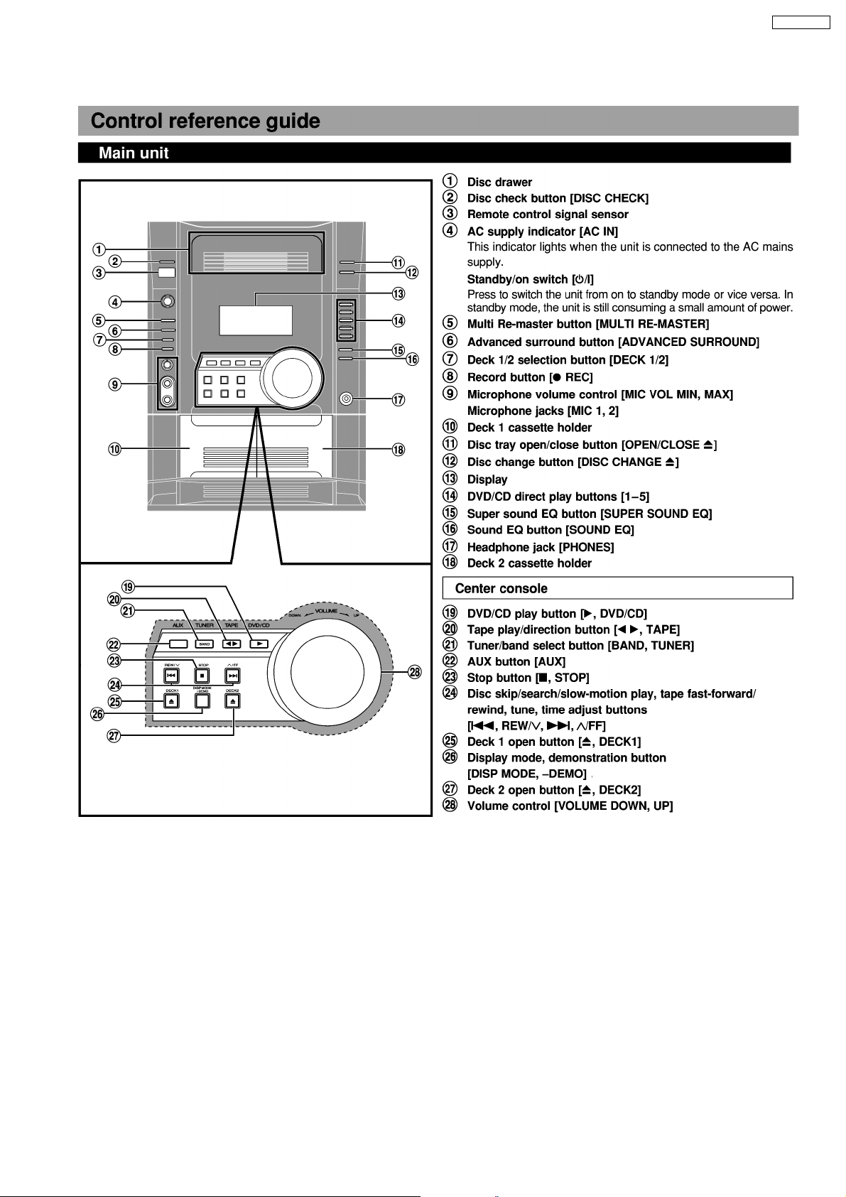
Page 1
A
A
A
A
A
*1
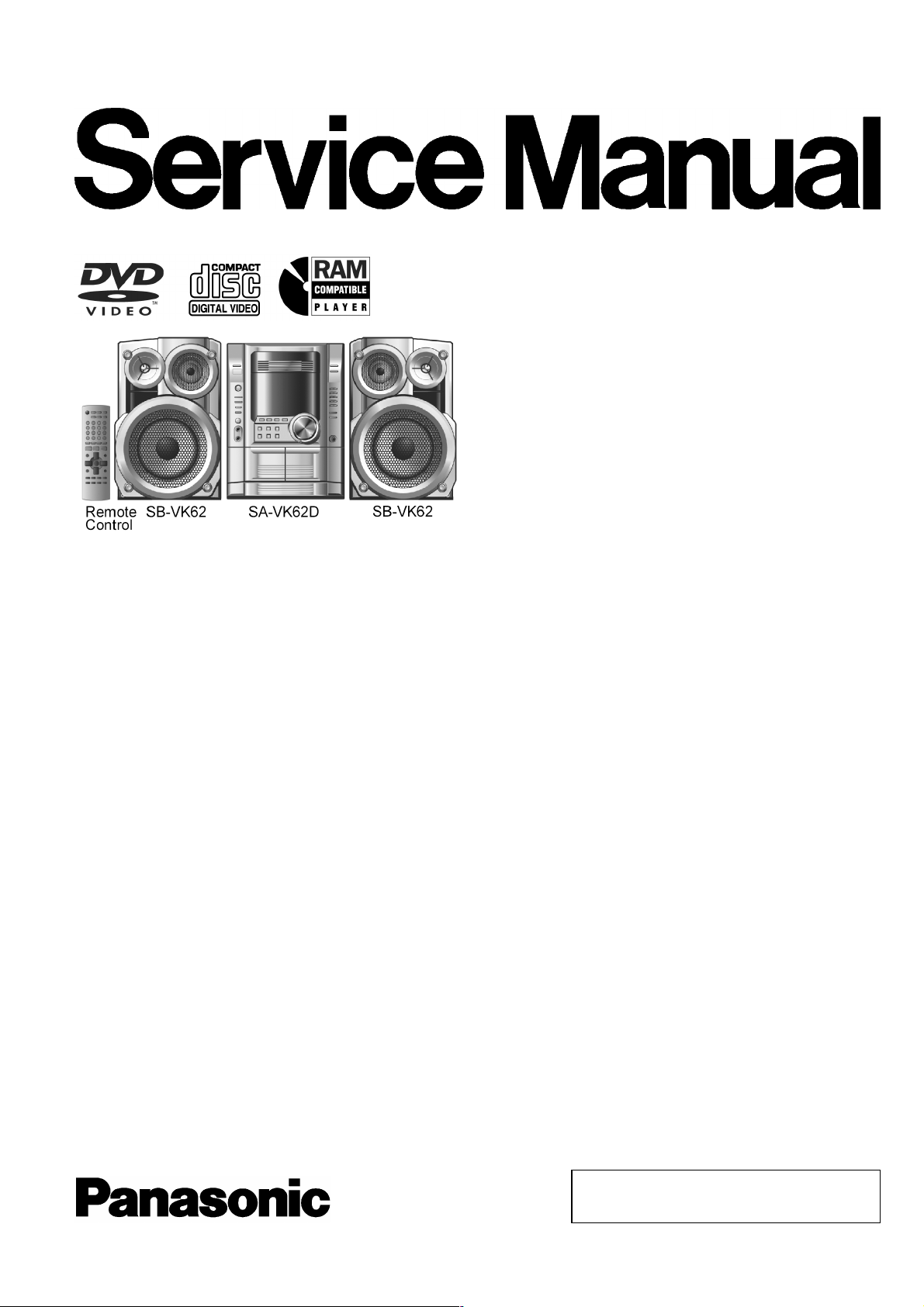
DVD Stereo System
SA-VK62DEE
Colour
(S)... Silver Type
ORDER NO. MD0504118C3
Specifications
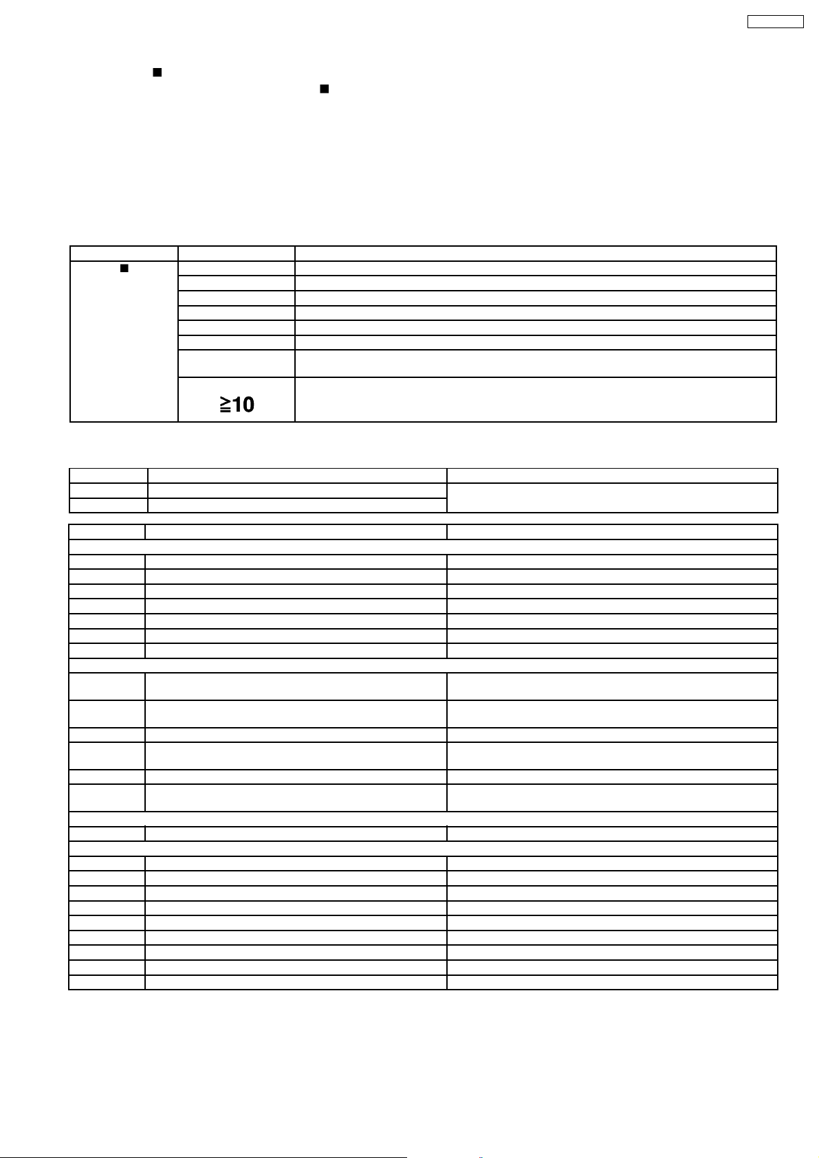
n AMPLIFIER SECTION
RMS Output Power Stereo Mode both channels driven:
10% Total Harmonic Distortion
1 kHz Front CH 110 W per channel (4 Ω )
Total RMS Stereo mode power 220 W
n FM/AM TUNER, TERMINALS SECTION
Preset station FM 15 stations
AM 15 stations
Frequency Modulation (FM)
Frequency range 87.50 - 108.00 MHz (50 kHz step)
Sensitivity 2.5 µV (IHF)
S/N 26dB 2.2 µV
ntenna terminals 75 Ω (unbalanced)
mplitude Modulation (AM)
Frequency range 522 - 1629 kHz (9 kHz step)
M Sensitivity S/N 20dB at 1000 kHz
560 µV/m
udio performance (Amplifier)
Input sensitivity/Input impedance
ux 250 mV, 12 kΩ
Digital audio output
Optical digital output Optical terminal
Phone jack
Terminal Stereo, 3.5 mm jack
Mic jack
Sensitivity 0.7 mV, 600 Ω
Terminal Mono, 6.3 mm jack (2 system)
n CASSETTE DECK SECTION
Type Auto-Reverse
Track system 4-Track, 2 Channel
Heads
Record/playback Solid permalloy head
Erasure Double gap ferrite head
Motor DC servo motor
Recording system AC bias 100 kHz
Erasing system AC erase 100 kHz
Tape speed 4.8 cm/s
Overall frequency response (+3, -6 dB) at DECK OUT
Normal 35 Hz - 14 kHz
S/N ratio 50 dB (A weighted)
Wow and flutter 0.18 % (WRMS)
Fast forward and rewind time Approx. 120 seconds with
C-60 cassette tape
n DISC SECTION
Disc played [8 cm or 12 cm]
(1) DVD (DVD-Video)
(2) DVD-RAM (DVD-VR, JPEG*4,*5)
(3) DVD-R/RW (DVD-Video)
+R/RW (Video)
(4) CD,CD-R/RW [CD-DA, Video CD, SVCD*1, MP3*2,*5, WMA*3,*5,
*4,*5
JPEG
, HighMAT Level 2 (Audio and Image)]
Conforming to IEC62107
© 2005 Matsushita Electric Industrial Co. Ltd.. All
rights reserved. Unauthorized copying and
distribution is a violation of law.
Page 2
*2
*3
*4
*5
A
SA-VK62DEE
Compatible compression rate: between 32 kbps and 320 kbps
Compatible compression rate: between 48 kbps and 320 kbps
Exif Ver 2.1 JPEG Baseline files
Picture resolution: between 320 x 240 and 6144 x 4096 pixels (Sub
sampling is 4:2:2 or 4:2:0)
The total combined maximum of recognizable audio, picture and
movie contents and groups: 4000 audio, picture and movie contents
and 400 groups.
Pick up
Wavelength
CD 785 nm
DVD 662 nm
udio output (Disc)
Number of channels (FL, FR) 2 ch (stereo)
n VIDEO SECTION
Video system PAL625/50, PAL525/60, NTSC
Composite video output
Output level 1Vp-p(75Ω)
Terminal Pin jack (1 system)
S-video output
Y output level 1Vp-p(75Ω)
C output level 0.3 Vp-p (75 Ω)(PAL)
0.286 Vp-p (75 Ω )(NTSC)
Terminal S terminal (1 system)
Component video output
Y output level 1Vp-p(75Ω)
PBoutput level 0.7 Vp-p (75 Ω)
PRoutput level 0.7 Vp-p (75 Ω )
Terminal
Pin jack (Y: green, PB:blue,PR:red)(1system)
n GENERAL
Power supply AC 230 V, 50Hz
Power consumption 193 W
Power consumption in standby mode:
0.9 W (approximate)
Dimensions (W x H x D) 250 x 364 x 330 mm
Mass 8kg
Operating temperature range +5 to +35°C
Operating humidity range 5 to 90% RH (no condensation)
n SYSTEM
SC-VK62D(EE) Music Center: SA-VK62D (EE)
Speaker: SB-VK62 (GC)
Notes:
1. Specifications are subject to change without notice. Mass and
dimensions are approximate.
2. Total harmonic distortion is measured by the digital spectrum
analyzer.
CONTENTS
Page Page
1 Before Repair and Adjustment
2 Protection Circuitry
3 Safety Precautions
3.1. General Guidelines
4 Prevention of Electro Static Discharge (ESD) to
Electrostatically Sensitive (ES) Devices
5 Handling the Lead-free Solder
5.1. About lead free solder (PbF)
6 Precaution of Laser Diode
7 Cautions to be taken when handling Optical Pickup
3
3
4
4
7.1. Handling Optical Pickup 9
7.2. Replacing Precautions for Optical Pickup Unit
7.3. Grounding for Preventing Electrostatic Destruction
8 Accessories
9 Operation Procedures
4
10 Disc information
6
11 About HighMAT
6
7
9
11.1. What 痴 HighMAT?
11.2. Why take advantage of HighMAT?
11.3. Benefits of HighMAT?
2
9
9
10
11
13
15
15
15
16
Page 3

SA-VK62DEE
12 Optical Pickup Self-Diagnosis and Replacement Procedure 19
12.1. Optical Pickup Breakdown diagnosis
13 Self-Diagnosis Function
13.1. Entering into Self-Diagnostic Mode
13.2. Automatic Displayed Error Codes
13.3. Memorized Error Codes
13.4. Service Mode Table 1
13.5. DVD/CD Self-Diagnosis Error Code Description
13.6. Mode Table 2
13.7. Doctor Mode set up
13.8. CR16 Mechanism Ageing Mode
13.9. Tray Lock Function
13.10. Things to Do After Repair
14 Cautions To Be Taken During Servicing
14.1. Recovery after the dvd player is repaired
14.2. DVD Player Firmware Version Upgrade Process
14.3. Firmware Version Upgrade Process by Using Disc and
Recovery Process
14.4. Using Recovery Disc
14.5. Total Usage Time Display
14.6. After replacement of DVD Module
15 Disassembly and Assembly of Main Component
15.1. Disassembly steps
15.2. Disassembly flow chart
15.3. Disassembly of Top Cabinet
15.4. Disassembly of Rear Panel
15.5. Disassembly of DVD Changer Unit
15.6. Disassembly of Main P.C.B.
15.7. Disassembly of Power P.C.B.
15.8. Disassembly of Transformer P.C.B.
15.9. Disassembly of Front Panel Unit
15.10. Disassembly for Panel P.C.B. & Mic P.C.B.
15.11. Disassembly for Tact Switch P.C.B.
15.12. Disassembly of Deck Mechanism Unit
15.13. Replacement for Traverse Deck
15.14. Replacement for Optical Pickup Unit (DVD mechanism)
15.15. Procedure for removing CD loading mechanism
15.16. CR16 mechanism disassembly procedure
15.17. CR16 mechanism assembly procedure
15.18. Disassembly for Traverse Unit
15.19. Replacement for the cassette lid ass 馳
15.20. Rectification for tape jam problem
19
20
20
20
20
21
21
21
23
24
24
24
25
25
25
25
25
25
26
27
27
28
29
29
29
30
31
32
32
33
33
34
34
35
38
38
44
56
57
58
16 Checking for major P.C.Bs
16.1. Checking of Main P.C.B.
16.2. Checking of Transformer P.C.B.
16.3. Checking of Panel, Deck & Deck Mechanism P.C.B.
16.4. Checking of Power P.C.B.
17 Measurements and Adjustments
17.1. Cassette Deck Section
17.2. Tuner Section
17.3. Alignment Points
18 Block Diagram
19 Schematic Diagram
19.1. Optical Pickup Unit Circuit
19.2. DVD Module Circuit
19.3. (A) Main (Tuner) Circuit
19.4. (B) Main Circuit
19.5. (C) Panel Circuit , (D) Tact Switch Circuit & (E) Mic Circuit
19.6. (F) Deck Circuit & (G) Deck Mechanism Circuit
19.7. (H) Power Circuit
19.8. (I) Transformer Circuit & (J) CD Loading Circuit
20 Printed Circuit Board
20.1. (A) DVD Module P.C.B. (Side: A & B )
20.2. (B) Main P.C.B.
20.3. (C) Panel P.C.B.
20.4. (D) Tact P.C.B. & (E) Mic P.C.B.
20.5. (F) Deck P.C.B. & (G) Deck Mechanism P.C.B.
20.6. (H) Power P.C.B.
20.7. (I) Transformer P.C.B.
20.8. (J) CD Loading P.C.B. & (K) Tuner Pack P.C.B.
21 Wiring Connection Diagram
22 Illustration of ICs, Transistors and Diodes
23 Terminal Function of IC
23.1. IC2801 (C2CBJG000639
24 Parts Location and Replacement Parts List
24.1. Deck Mechanism (RAA3413-S)
24.2. DVD Loading Mechanism
24.3. Cabinet
24.4. Electrical Parts List
24.5. Packing Materials & Accessories Parts List
24.6. Packaging
) System Microprocessor
59
59
60
61
62
63
63
64
65
66
76
77
78
85
86
93
96
98
99
100
100
102
104
106
107
108
110
111
112
114
115
115
117
118
121
124
127
138
139
1 Before Repair and Adjustment
Disconnect AC power, discharge Power Supply Capacitors C5820, C5840 and C5950 through a 10Ω, 5W resistor to ground.
DO NOT SHORT-CIRCUIT DIRECTLY (with a screwdriver blade, for instance), as this may destroy solid state devices.
After repairs are completed, restore power gradually using a variac, to avoid overcurrent.
Current consum ption at AC 230V, 50Hz in NO SIGNAL (vol. min, at CD mode) should be ~500mA .
2 Protection Circuitry
The protection circuitry may have operated if either of the following conditions are noticed :
3
Page 4
SA-VK62DEE
No sound is heard when the power is turned on.
·
Sound stops during a performance.
·
The function of this circuitry is to prevent circuitry damage if, for example, the positive and negative speaker connection wires are
“shorted”, or if speaker systems with an impedance less than the indicated rated impedance of the amplifier are used.
If this occurs, follow the procedure outlines below:
1. Turn off the power.
2. Determine the cause of the problem and correct it.
3. Turn on the power once again after one minute.
Note :
When the protection circuitry functions, the unit will not operate unless the power is first turned off and then on again.
3 Safety Precautions
3.1. General Guidelines
1. When servicing, observe the original lead dress. If a short circuit is found, replace all parts which have been overheated or
damaged by the short circuit.
2. After servicing, see to it that all the protective devices such as insulation barriers, insulation papers shields are properly
installed.
3. After servicing, make the following leakage current checks to prevent the customer from being exposed to shock hazards.
3.1.1. Leakage Current Cold Check
1. Unplug the AC cord and connect a jumper between the two prongs on the plug.
2. Measure the resistance value, with an ohmmeter, between the jumpered AC plug and each exposed metallic cabinet part on
the equipment such as screwheads, connectors, control shafts, etc. When the expose d metallic part has a return path to the
chassis, the reading should be between 1MΩ and 5.2MΩ.
When the exposed metal does not have a return path to the chassis, the reading must be ・.
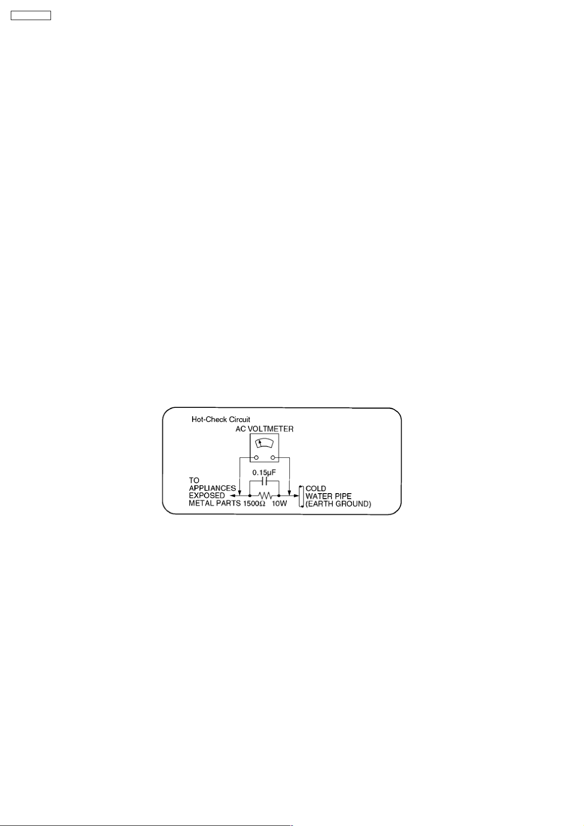
Figure 1
3.1.2. Leakage Current Hot Check
(See Figure 1)
1. Plug the AC cord directly into the AC outlet. Do not use an isolation transformer for this check.
2. Connect a 1.5kΩ, 10 watts resistor, in parallel with a 0.15µF capacitor, between each exposed metallic part on the set and a
good earth ground such as a water pipe, as shown in Figure 1.
3. Use an AC voltmeter, with 1000 ohms/volt or more sensitivity, to measure the potential across the resistor.
4. Check each exposed metallic part, and measure the voltage at each point.
5. Reverse the AC plug in the AC outlet and repeat each of the above measurements.
6. The potential at any point should not exceed 0.75 volts RMS. A leakage current tester (Simpson Model 229 or equivalent) may
be used to make the hot checks, leakage current must not exceed 1/2 milliamp. In case a measurement is out of the limits
specified, there is a possibility of a shock hazard, and the equipment should be repaired and rechecked before it is returned to
the customer.
4 Prevention of Electro Static Discharge (ESD) to
Electrostatically Sensitive (ES) Devices
Some semiconducto r (solid state) devices can be damaged easily by electricity. Such components commonly are called
4
Page 5
SA-VK62DEE
Electrostatically Sensitive (ES) Devices. Examples of typical ES devices are integrated circuits and some field-effect transistors and
semiconductor “chip” components. The following techniques should be used to help reduce the incidence of component damage
caused by electro static discharge (ESD).
1. Immediately before handling any semiconductor component or semiconductor-equipped assembly, drain off any ESD on your
body by touchin g a known earth ground. Alternatively, obtain and wear a commercially available discharging ESD wrist strap,
which should be removed for potential shock reasons prior to applying power to the unit under test.
2. After removing an electrical assembly equipped with ES devices, place the assembly on a conductive surface such as
aluminium foil, to prevent electrostatic charge build up or exposu re of the assembly.
3. Use only a grounded-tip soldering iron to solder or unsolder ES devices.
4. Use only an anti-static solder remover device. Some solder removal devices not classified as “anti-static (ESD protected)” can
generate electrical charge to damage ES devices.
5. Do not use freon-propelled chemicals. These can generate electrical charges sufficient to damage ES devices.
6. Do not remove a replacement ES device from its protective package until immediately before you are ready to install it. (Most
replacement ES devices are packaged with leads electrically shorted together by conductive foam, aluminium foil or
comparable conductive material).
7. Immediately before removing the protective material from the leads of a replacement ES device, touch the protective material
to the chassis or circuit assembly into which the device will be installed.
Caution
Be sure no power is applied to the chassis or circuit, and observe all other safety precautions.
8. Minimize body motions when handling unpackaged replacement ES devices. (Otherwise harmless motion such as the brushing
together of your clothes fabric or the lifting of your foot from a carpeted floor can generate static electricity (ESD) sufficient to
damage an ES device).
5
Page 6

SA-VK62DEE
5 Handling the Lead-free Solder
5.1. About lead free solder (PbF)
Distinction of PbF P.C.B.:
P.C.B.s (manufactured) using lead free solder will have a PbF stamp on the P.C.B.
Caution:
· Pb free solder has a higher melting point than standard solder; Typically the melting point is 50 - 70°F (30 - 40°C) higher. Please
use a high temperature soldering iron. In case of soldering iron with temperature control, please set it to 700 ± 20°F (370 ±
10°C).
· Pb free solder will tend to splash when heated too high (about 1100°F/600°C).
· W hen soldering or unsoldering, please completely remove all of the solder on the pins or solder area, and be sure to heat the
soldering points with the Pb free solder until it melts enough.
6
Page 7

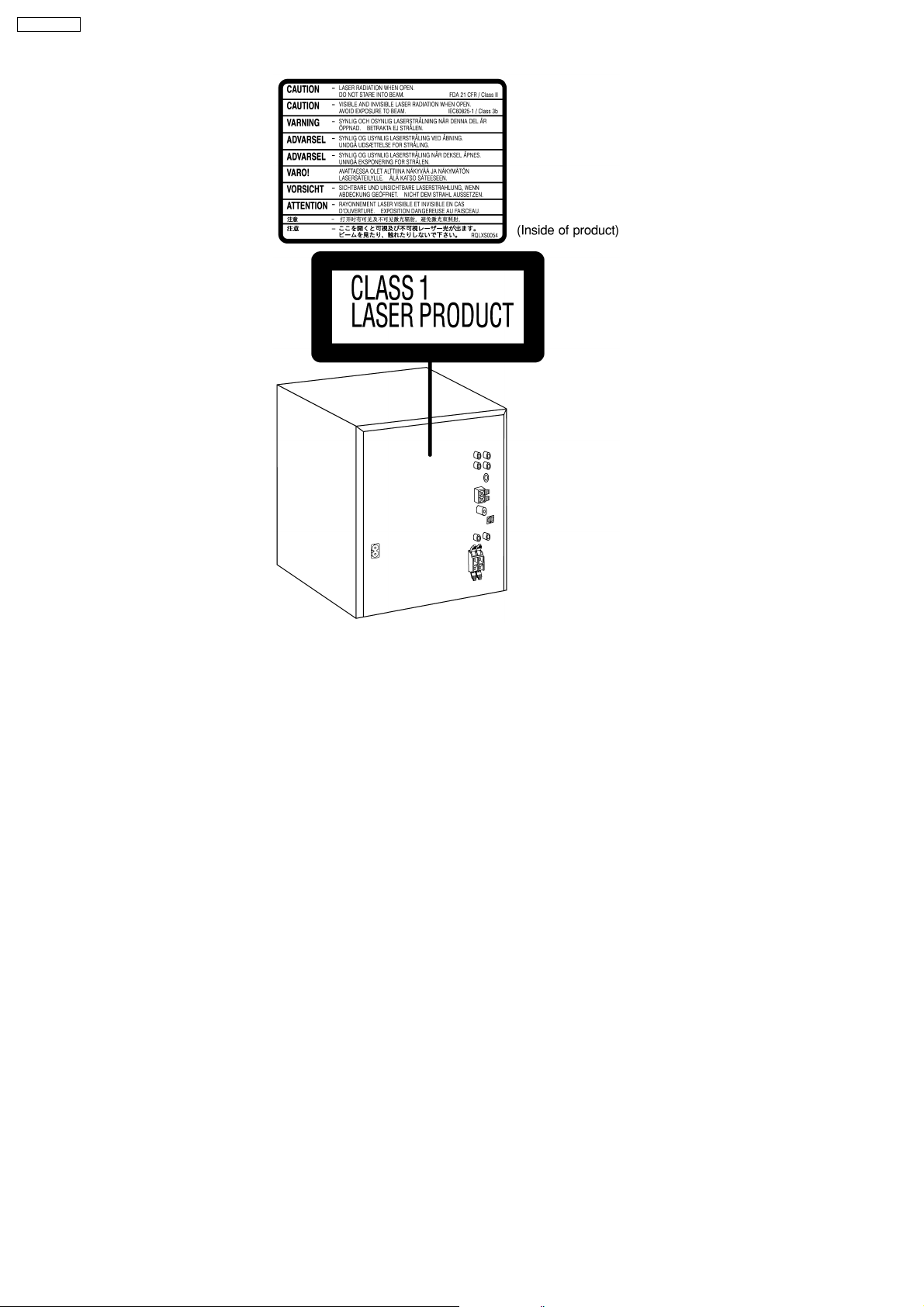
6 Precaution of Laser Diode
Caution :
This product utilizes a laser diode with the unit turned "ON", invisible laser radiation is emitted from the pick up lens.
Wavelength : 785 nm(CD)/662 nm(DVD)
Maximum output radiation power from pick up : 100 µW/VDE
Laser radiation from pick up unit is safety level, but be sure the followings:
1. Do not disassemble the optical pick up unit, since radiation from exposed laser diode is dangerous.
2. Do not adjust the variable resistor on the pick up unit. It was already adjusted.
3. Do not look at the focus lens using optical instruments.
4. Recommend not to look at pick up lens for a long time.
ACHTUNG :
Dieses Produkt enthält eine Laserdiode. Im eingeschalteten Zustand wird unsichtbare Laserstrahlung von der Lasereinheit
abgestrahlt.
Wellenlänge : 785nm (CD)/662 nm(DVD)
Maximale Strahlungsleistung der Lasereinheit :100 µW/VDE
Die Strahlung an der Lasereinheit ist ungefährlich, wenn folgend e Punkte beachtet werden:
1. Die Lasereinheit nicht zerlegen, da die Strahlung an der freigelegten Laserdiode gefährlich ist.
2. Den werkseitig justierten Einstellregler der Lasereinhit nicht verstellen.
3. Nicht mit optischen Instrumenten in die Fokussierlinse blicken.
4. Nicht über längere Zeit in die Fokussierlinse blicken.
SA-VK62DEE
ADVARSEL: I dette a apparat anvendes laser.
CAUTION!
THIS PRODUCT UTILIZES A LASER.
USE OF CONTROLS OR ADJUSTMENTS OR PERFORMANCE OF PROCEDURES OTHER THAN THOSE SPECIFIED HEREIN MAY RESULT
IN HAZARDOUS RADIATION EXPOSURE.
n Use of caution label
7
Page 8
SA-VK62DEE
8
Page 9
SA-VK62DEE
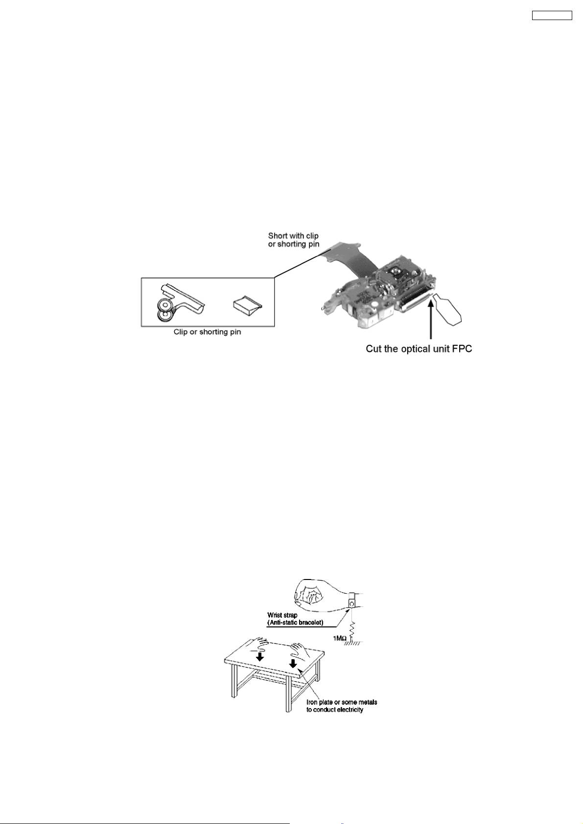
7 Cautions to be taken when handling Optical Pickup
The laser diode used inside optical pickup could be destroyed due to static electricity as a potential difference is caused by
electrostatic load discharged from clothes or human body. Handling the parts carefully to avoid electrostatic destruction during
repair.
7.1. Handling Optical Pickup
1. Do not impact on optical pickup as the unit structurally uses an extremely precise technology.
2. Short-circuit the flexible cable of optical pickup remove from the circuit board using a short-circuit pin or clip in order to prevent
laser diode from electrostatic destruction (Refer to Fig. 7.1 and Fig. 7.2)
3. Do not handle flexible cables forcibly as this may cause snapping. Handle the parts carefully (Refer to Fig. 7.1)
4. A new optical pickup is equipped with an anti-static flexible cable. After replacing and connecting to the flexible board, cut the
anti-static flexible cable. (Refer to Fig. 7.1)
Fig. 7.1
7.2. Replacing Precautions for Optical Pickup Unit
DVD/CD Optical Pickup
The optical pickup by which part supply was carried out attaches the short clip to the flexible board for laser diode electrostatic
discharge damage prevention. Please remove the short clip and be sure to check that the short land is open, before connecting.
(Please remove solder, when the short land short-circuits.)
7.3. Grounding for Preventing Electrostatic Destruction
1. Human body grounding
Use the anti-static wrist strap to discharge the static electricity accumulated in your body. (Refer to Fig. 7.2)
2. Work place grounding
Place a conductive material (conductive sheet) or iron board where optical pickup is placed . (Refer to Fig. 7.2)
Note :
Keep your clothes away from optical pickup as wrist strap does not release the static electricity charged in clothes.
Fig. 7.2
9
Page 10
SA-VK62DEE
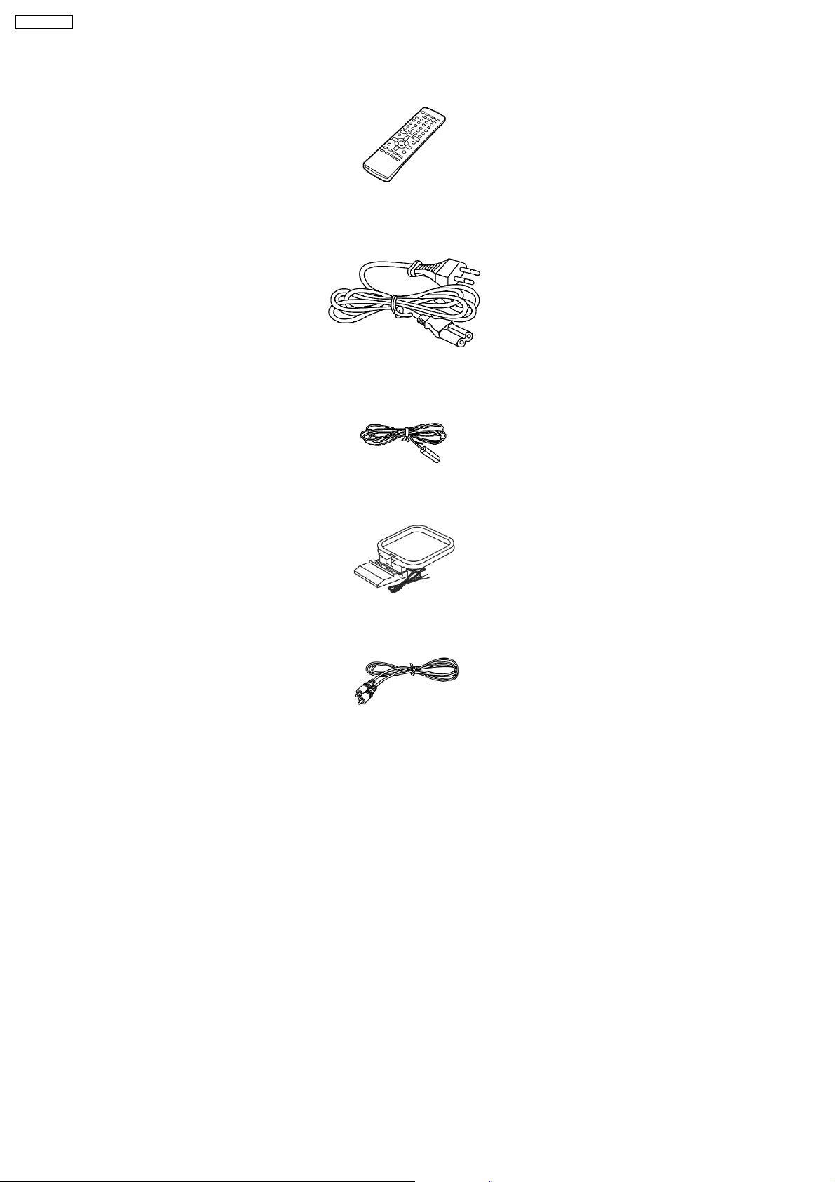
8 Accessories
Remote control
AC power supply cord
FM indoor antenna
AM loop antenna
Video cable
10
Page 11
9 Operation Procedures
SA-VK62DEE
11
Page 12
SA-VK62DEE
12
Page 13
10 Disc information
SA-VK62DEE
13
Page 14
SA-VK62DEE
14
Page 15

SA-VK62DEE
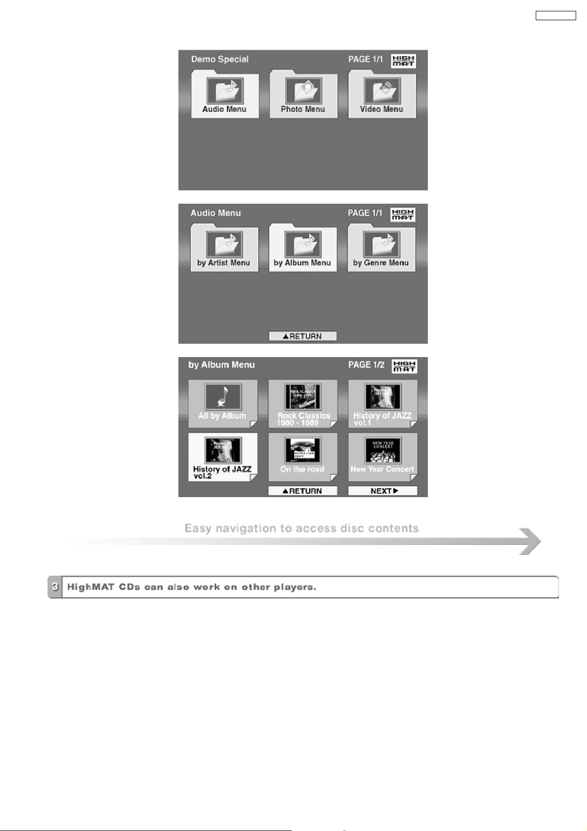
11 About HighMAT
11.1. What’s HighMAT?
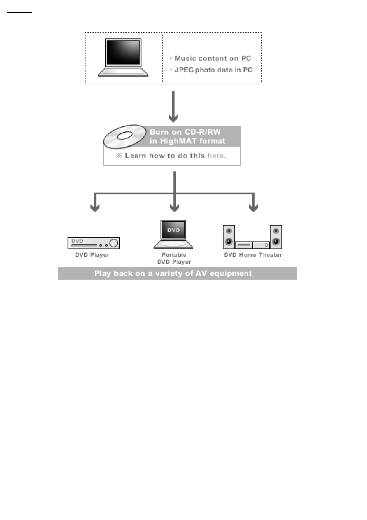
Consumers worldwide are using PCs to create their own collections of music, photos and even video by burning them onto CDs.
But how these collections can be experienced across different devices can be confusing to navigate, time consum ing to access for
a DVD player, and be incomplete in terms of music information available to the customer.
HighMAT offers a solution to this growing consumer problem. HighMAT dramatically improves the digital media experience on
consumer electronic devices by delivering a simple, standardized approach that allows consumers who have created personal
collections of digital music, photography and video on their PC to:
>> Create a HighMAT CD or DVD which can be easily played back on consum er electronics devices such as CD and DVD players ,
and car stereos.
>> Move digital media files (using recordable media such as CD-R and CD-RW) between the PC and various playba ck devices
such as CD and DVD players.
A new standard for creating personal media on consumer electronic devices, HighMAT enable easier and more seamless
interoperability between Windows PCs and devices designed for your living room, or the car.
11.2. Why take advantage of HighMAT?
A Problem Defined:Toda y, when consumers create their own digital audio, video or photo collections on CD-R or other physical
formats, there are numerous, inconsistent ways that devices read the data. For the consumer, the playback experience can be
confusing:
15
Page 16
SA-VK62DEE
A Solution Created: HighMAT delivers a better digital media access experience by creating a standard approach for PCs to
structure digital media on various physical formats and for playback devices to read the data.
11.3. Benefits of HighMAT?
Conventional HighMAT
Even though DVD player is CD-R/RW compatible, the inconsistent ways
that various DVD players can read the music or photos files often leads
to a confusing and inconsistant playback experince.
HighMAT compatible products play content back with consistent
interface. This includes products which are JPEG compatible products
without HighMAT support.
16
Page 17
SA-VK62DEE
17
Page 18
SA-VK62DEE
HighMAT is now available for CD Burning and in Leading DVD PlayersHighMAT is a new technology that is now available in leading
software and consumer electronic devices to dramatically improve the digital media experience when you create homemade
CDsHighMAT delivers a simple, standardized way for PC software and consumer electronics devices to talk to each other and work
better together.
When you create your homemade CDs with software that supports HighMAT CD burning, and then play them back on a DVD
player that supports HighMAT, you get better, easier navigation. You get folders you can access with a single click of your DVD
player´s remote control. You can view important information about your music like full song names, artist titles, album names and
genre. And you can get faster startup on your home entertainment device.
To enjoy the benefits of HighMAT, all you need is software that supports HighMAT for CD burning of music or photos, as well as
a home entertainment device like a DVD player that supports HighMAT for playback. Always look for the HighMAT logo on your
software or home entertainment device to ensure it supports the HighMAT experience.
18
Page 19
SA-VK62DEE
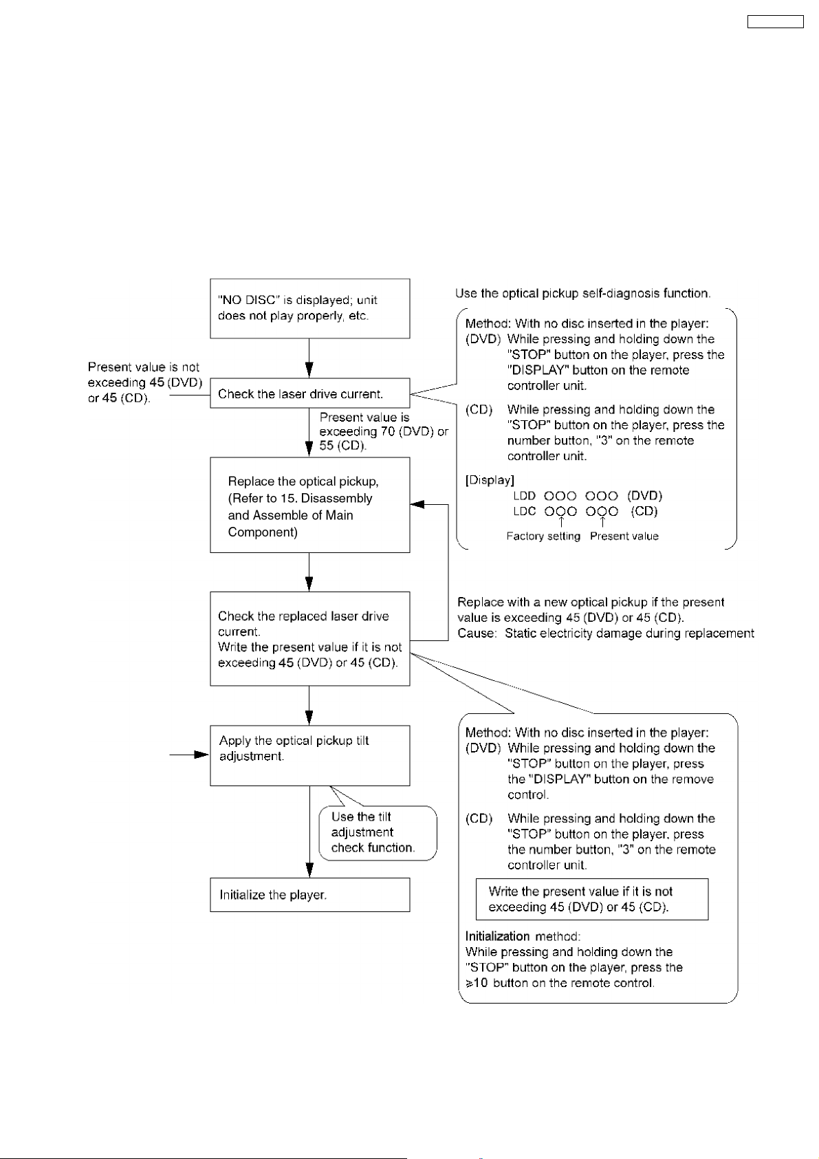
12 Optical Pickup Self-Diagnosis and Replacement
Procedure
12.1. Optical Pickup Breakdown diagnosis
This unit is equipped with the optical pickup self-diagnosis function and the tilt adjustment check function. Follow the procedure
described below during repair in order to perform self-diagnosis and tilt adjustment effectively. Especially when “NO DISC” is
displayed, be sure to apply the self-diagnosis function before replacing with an optical pickup. Replacement of optical pickup
generally requires when the present value of laser drive exceeds 45 (DVD) or 45 (CD).
Note:
Start diagnosis within three minutes after turning on the power (as diagnosis fails when the unit becomes warm).
19
Page 20
SA-VK62DEE
13 Self-Diagnosis Function
This unit is equipped with the self-diagnosis function, which display s an error when it occurs, for use during servicing.
13.1. Entering into Self-Diagnostic Mode
13.2. Automatic Displayed Error Codes
13.2.1. Automatic Display Function
For a power unit error, the code is automatically display ed.
F61: Automatically display ed on the LCD of the player.
13.2.2. Re-Display
· For F61 Display
−
− When the code, F61 is displayed, the power is automatically turned off.
− −
−
− The code, F61 is displayed for three seconds, and then the current time appears.
− −
−
− To retrieve the code, turn on the power button so that the code F61 appears, however, is switched to time display after three
− −
seconds, and the power is automatically turned off.
· For F76 Display
−
− The abnormalities is an output or the abnormalities in a power supply of POWER AMP IC.
− −
13.2.3. Description of Error Code
13.2.3.1. F61
· State, Condition
When the power is turned on, the unit is automatically turned off. The power does not turn on.
· Cause, Troubleshooting
Power circuit system failure and/or direct current flown to speaker terminal
Identify the cause and replace with new parts.
13.3. Memorized Error Codes
13.3.1. Activating Self-Diagnosis Function and Displaying Method
1. Turn on the power.
2. Select DVD/CD function. With no DVD/CD inserted in the player, press and hold down the
and press the “0” button on the remote control for at least two seconds in order to display “DVD_F_ _ _ ”.
20
button for at least two seconds,
Page 21
3. Press the button. If a memorized error is detected, the result of self diagnosis is displayed. (Ex.: T H15)
If several errors are detected, press the
button to display each.
13.3.2. Re-Display
· Press the power button to turn off the power, and then turn on the power.
· The details of self diagnosis are stored in the unit memory.
To retrieve them, follow the procedure described the above, “Activating Self-Diagnosis Function and Displaying Method”.
13.4. Service Mode Table 1
Following modes are available with combinations of the pressed buttons on the player and on the remote controller unit.
Player Remote Controller Unit Usage
button
0 Error code display (Refer to the Item 13.5. DVD/CD Self-Diagnosis Error Code Description)
5 Tilt adjustment (Jitter)
6 Region number and broadcasting system check
8 Bulit-in program version check (Micro-P)
DISPLAY DVD laser drive current check
3 CD laser drive current check
PAUSE Writing of laser drive current value after replacement of optical pickup
(Do use this function only when optical pickup is replaced.)
Initialization of the player (factory setting is restored.)
Used after replacement of micro-computer and its peripherals and printed circuit board.
SA-VK62DEE
13.5. DVD/CD Self-Diagnosis Error Code Description
Error Code State, Conditon Cause, Troublesh ooting
H15 The disc tray cannot be opened: it closes spontaneously. Disc tray open/close detection switch (S1001) failure.
H16 The disc tray cannot be closed: it opens spontaneously.
Error Code Meaning Details
U. H. Error
U11 Focus servo failure
H01 Tray loading failure
H02 Spindle servo failure (Spindle servo, DSC, SP motor, CLV servo failure)
H03 Traverse motor failure
H04 Tracking servo error
H05 Seek timeout failure
H06 Power supply error
DSC system
F500 DSC failure DSC stops due to servo failure.
F501 DSC not Ready failure Communication failure between DSC and system computer
F502 DSC Time out failure See F500.
F503 DSC communication failure Communication failure (Result failure occurs after communication
F505 DSC Attention Error See F500.
F506 Invalid media Disc is placed upside down; TOC is unreadable or invalid disc is
Disc Code
F103 Ilegal highlight position Disc standard is possibly illegal when highlight is displayed.
IIC Error
F4FF Forced initialization failure (Time out)
F880 Unsuitable task number When a message arrives from not existing task
F890 A message is sent during AV task transmission During transmission of a message to AV task
F891 Unable to transmit a message to AV task When transmission of a message to AV task starts
F893 DVD Module problem Check for firmware version
F894 EEPROM failure
F895 Firmware compatibility problem Check for firm version for Main & DVD Module P.C.B.
F897 Initialization is not done properly Follow proper steps for initialization & reset
F8A0 Unsuitable message command When transmission of a message to AV task starts
(Check and replace)
(Startup, focus failure, etc.)
(No communication because DSC does not move)
command is transmitted.)
inserted.
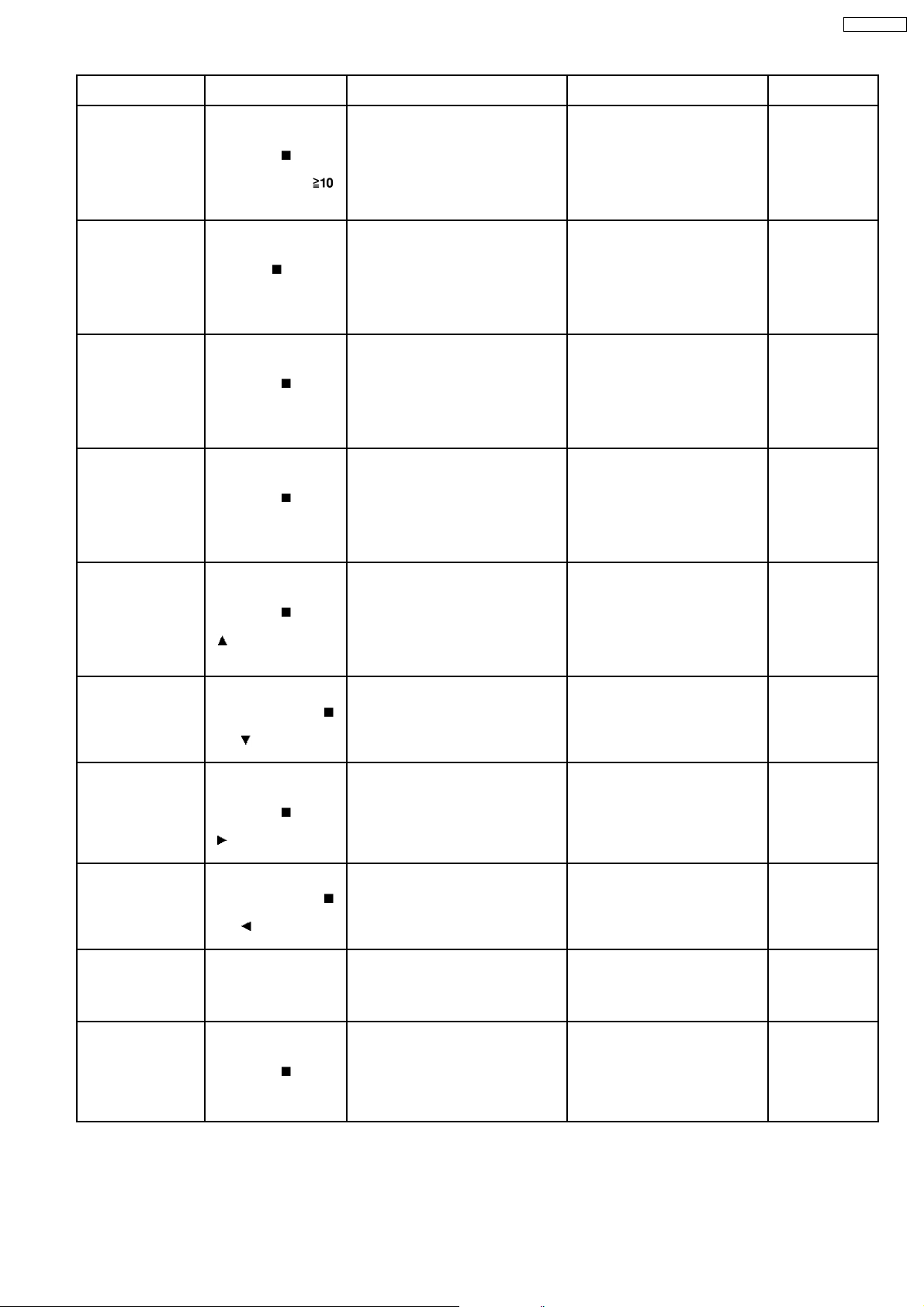
13.6. Mode Table 2
Following modes are available with combinations of the pressed buttons on the player and on the remote controller unit.
21
Page 22
SA-VK62DEE
Item Operational Condition
and Key Function
Jitter display While the player is
stopped and no disc is
inserted, press and hold
down the
button
on the player and the
number button, “5” on
the remote controller
unit.
Error code display While the player is
stopped and no disc is
inserted, press and hold
down the
button
on the player and the
number button, “0” on
the remote controller
unit.
Measurement of laser
current electricity
initialization value
While the player is
stopped and no disc is
inserted, press and hold
down the
button
on the player and the
button on the
remote controller unit.
Details Display TO Exit Mode
Jitter display
Measures and displays jitter.
Measurement is repeated every
second. Read error counter starts at 0
at the mode setting, and increased by
one as data read fails at target block. A
small defect is allowed to correct by
retry. Any possibility is counted as one
increment. Repetitive errors after retry
increase by two levels or more.
Error code display
Displays the latest error code stored in
EEPROM.
Measurement of laser current
electricity initialization value
Memorizes each initialization value of
DVD and CD in EEPROM.
J*1xxx*2_yyy*3_zz
*1
: Jitter display mode
*2
: Jitter measurement value
*3
: Read error counter
*4
: Focus driving value
*4
Values are shown to one decimal
place in the decimal digit. Focus
driving value is displayed in the
hexadecimal digit.
DVDnn_F---
*nn: Error history
*--: Error number
DVD 01 FOBF
LDO*1_013*2_032
*1
: Laser current electricity
measurement mode
*2
: DVD current electricity value
*3
: CD current electricity value
*3
Press the STOP or
OPEN button.
Press the OPEN
button.
Automatically exits
the mode after five
seconds.
Measurement of DVD
laser current electricity
ADSC internal RAM
display
Measurement of CD
laser current electricity
While the player is
stopped and no disc is
inserted, press and hold
down the
button
on the player and the
DISPLAY button on the
remote controller unit.
While the player is
stopped and no disc is
inserted, press and hold
down the
button
on the player and the
number button “1” or “2”
on the remote controller
unit.
While the player is
stopped and no disc is
inserted, press and hold
down the
button
on the player and the
number button “3” on the
remote controller unit.
Measurement of DVD laser current
electricity
Measures DVD laser current electricity
and displays the result together with
the initialization value stored in
EEPROM. After measurement, DVD
laser is lit till the power is turned off (or
goes off when the primary power is
turned off).
ADSC internal RAM display
Reads and displays the RAM value
inside ADSC. The address is renewed
when the CLEAR key is pressed so
that the values at eleven points appear.
Measurement of CD laser current
electricity
Measures CD laser current electricity
and displays the result together with
the initialization value stored in
EEPROM. After measurement, CD
laser is lit till the power is turned off (or
goes off when the primary power is
turned off).
Values are shown in the decimal
digit. The above example indicates
that the current electricity
initialization value is 13mA at DVD
laser and 32mA at CD laser when
laser is turned on.
LDD*1_012*2_014
*1
: DVD laser current electricity
measurement mode
*2
: Current electricity initialization
value stored in EEPROM
*3
: Present value of current
*3
electricity
Values are shown in the decimal
digit. The above example indicates
that the current electricity
initialization value is 12mA and its
present value is 14mA.
FB0 0000
Values are shown in the
hexadecimal digit. The above
example indicates that ADSC
value at the address, FB0h is
0000h.
LDC*1_032*2_032
*1
: CD laser current electricity
measurement mode
*2
: Current electricity initialization
value stored in EEPROM
*3
: Present value of current
*3
electricity
Automatically exits
the mode after five
seconds.
Press the STOP or
OPEN button.
Automatically exits
the mode after five
seconds.
22
Values are shown in the decimal
digit. The above example indicates
the current electricity initialization
value is 28mA and its present
value is 26mA when laser is turned
on.
Page 23
SA-VK62DEE
Item Operational Condition
and Key Function
User initialization While the player is
stopped and no disc is
inserted, press and hold
down the
button
on the player and the
number button
on the remote controller
unit.
Region display While the player is
stopped and no disc is
inserted, press and hold
down the
button on
the player and the
number button, “6” on
the remote controller
unit.
Firmware version
display
While the player is
stopped and no disc is
inserted, press and hold
down the
button
on the player and the
number button, “7” on
the remote controller
unit.
Region and firmware
display
While the player is
stopped and no disc is
inserted, press and hold
down the
button
on the player and the
number button, “8” on
the remote controller
unit.
Laser use time While the player is
stopped and no disc is
inserted, press and hold
down the
button
on the player and the
button on the
remote controller unit.
Reset laser use time While the usage time 1 is
displayed, press and
hold down the
button on the player and
the
button on the
remote controller unit.
Spindle use time While the player is
stopped and no disc is
inserted, press and hold
down the
button
on the player and the
button on the
remote controller unit.
Reset spindle use
time
While the usage time 2 is
displayed, press and
hold down the
button on the player and
the
button on the
remote controller unit.
User reset While the player is
stopped and no disc is
inserted, press “STOP” &
“ENTER” on remote
control.
Communication error
display
While the player is
stopped and no disc is
inserted, press and hold
down the
button
on the player and the
MENU button on the
remote controller unit.
Details Display TO Exit Mode
User initialization
“INIT” The user setting recovers the factory
setting.
Region display [xx yy zz]
Automatically exits
the mode after five
s : Panecon model type
seconds.
rrr : Panecon release number
x : Syscon generation (45)
y: Syscon model type
zzz: Syscon release number
Firmware version display rrr*1_xx*2y*3zzz
*1
: Panel computer release number
*2
: System computer generation
*3
: System computer model type
*4
: System computer release
*4
Automatically exits
the mode after five
seconds.
number
Region and firmware version display xx yy zz
*1
: Region number
*2
: System computer generation
*3
: System computer model type
*4
: System computer release
Automatically exits
the mode after five
seconds.
number
Laser usage time
Measures each for DVD and CD
respectively.
T1 1234
The numbers in the left show
Automatically exits
the mode after five
seconds.
usage time for DVD laser and
those in the right for CD laser. The
four-digit number is shown by the
ten hours in the decimal digit. The
number after 0000 is 9999.
Laser usage time reset
Resets both for DVD and CD at once.
T1 0000 Automatically exits
the mode after five
seconds.
Spindle motor usage time T2 00000
Automatically exits
the mode after five
The four-digit number is shown by
seconds.
the ten hours in the decimal digit.
The number after 00000 is 99999.
Usage time 2 reset
Spindle motor usage time
T2_0000 Automatically exits
the mode after five
seconds.
Reset the unit. “DVD RESET” Automatically exits
the mode after five
seconds.
Displays frequency of communication
errors between system computer firm
IC and mechanical computer IC during
ECC 00 Automatically exits
the mode after five
seconds.
DVD module.
13.7. Doctor Mode set up
1. Turn on power for the unit.
2. Select DVD/CD Mode. Ensure no disc is inserted in the unit.
23
Page 24
SA-VK62DEE
3. Press and hold [STOP] button on main unit at least 3 seconds, follow by [3] on the remote control. It enters into doctor mode.
4. Press [POWER] button on main unit or remote control to exit doctor mode.
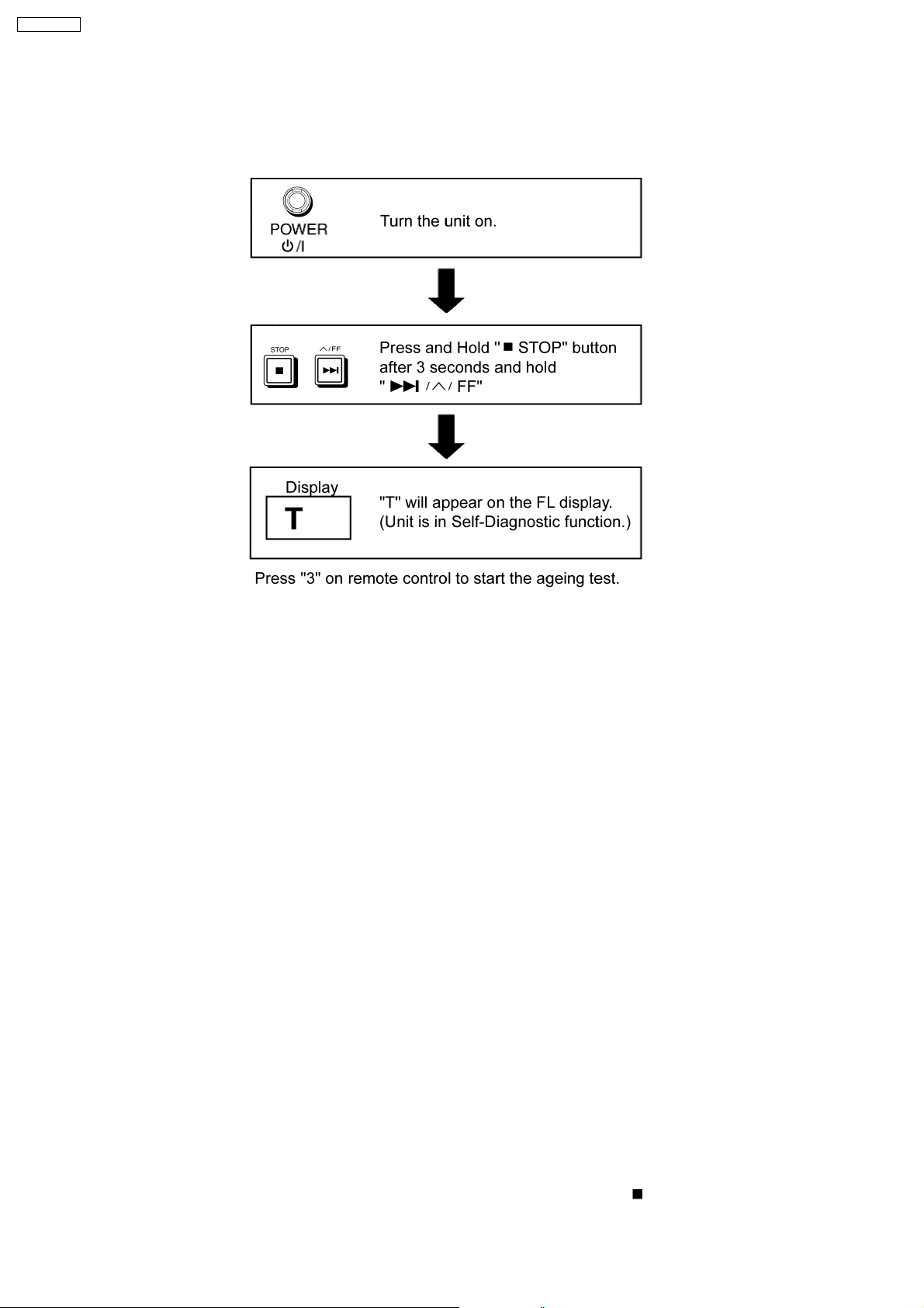
13.8. CR16 Mechanism Ageing Mode
To perform the ageing mode:
1. Enter into doctor mode. (Refer to Section 13.7 Doctor Mode set up) as mentioned above.
2. Press [3] button on remote control. It enters into ageing mode. (see below for ageing process)
Ageing process:
1. Tray 1 open.
2. It waits for one second (Note: Do not put any disc into the tray.
3. Tray close.
4. TOC READ (Reading incomplete)
5. Tray 2 open & repeat step 1 to step 4. (Process repeat until Tray 5)
6. Tray check.
7. Whole process complete (Counter on FL increase by 1)
Note: To exit ageing mode, press [POWER] button. The unit will power down. Do not unplug the power cord until FL display shows
“GOODBYE”. This is to avoid tray jam problem.
13.9. Tray Lock Function
13.9.1. Setting
· Disc Lock Function
1. With the SELECTOR on DVD/CD and POWER ON, hold down the [
[POWER] KEY on the remote control for 3 seconds to enter to Lock mode A.[_ _ _LOCKED_] will be display ed for 3
seconds, and then current disc will begin playing .
2. In Lock mode A, the following key is disabled.
[OPEN/CLOSE]
· Operation Lock Function
1. With the SELECTOR on DVD/CD and POWER ON, hold down the [CD PLAY] KEY on the main unit, and then press the
[POWER] KEY on the remote control for 3 seconds to enter Lock mode B.
[_ _ _ LOCKED_] will be displayed for 3 seconds, and the current disc will begin playing.
2. Lock mode B primarily controls the selector and disc operations, and disenables for the following keys.
Note:
OPEN/CLOSE
· Prohibiting operation of selector and disk
1. Select the DVD/CD function.
2. Press and hold down the
seconds. (The message, “___LOCKED_” appears when the function is activated.)
Note:
The following buttons are invalid and the player displays “___LOCKED_” while the lock function mode is entered.
button are invalid and the player displays “___LOCKED _” while the lock function mode is entered.
button on the player and the power button on the remote controller unit for at least three
STOP] KEY on the main unit, and then press the
13.10. Things to Do After Repair
Follow the procedure described below after repair.
1. While the power is on, press the
2. Press the power button to turn off the power.
3. Unplug the power cable.
button to close the tray.
24
Page 25

SA-VK62DEE
Note:
It is prohibited to unplug the power cable while the tray is opened and to close the tray manually.
14 Cautions To Be Taken During Servicing
14.1. Recovery after the dvd player is repaired
· W hen Flash ROM or DVD Module P.C.B. is replaced, carry out the recovery processing to optimize the drive. Playback the
recovery disc to process the recovery automatically.
· Recovery disc (Product number=RFKZD03R005)
· Performing recovery
1. Load the recovery disc (Product number: RFKZD03R005) to the player and run it.
2. Recovery is performed automatically . When it is finished, a message appears on the screen.
3. Remove the recovery disc.
4. Turn off the power.
14.2. DVD Player Firmware Version Upgrade Process
Firmware of DVD player may upgrade to conform to improvement of its performance and quality including operational range,
playability of non-standardized discs, etc. The version upgrade disc contains the recovery function, and the recovery disc is not
necessary.
Note:
Version upgrade process cannot be complete if the AC power is cut off due to power failure and other occasions during the
process. If this occurs, replace FLASH ROM IC and restart version upgrade. Version upgrade disc number is informed when
ordered.
14.3. Firmware Version Upgrade Process by Using Disc and Recovery
Process
· Recovery process
· Firmware version upgrade process
Both of the above procedures automatically start when the recovery disc is replayed.General CD-R disc allows version upgrade
process and recovery process, making version upgrade through disc simple.
Recovery process: Optimization process of player after replacement of FLASH ROM, EEPROM, or module circuit board
Version upgrade process: Renewal of firmware for improvement of operational range and performance
14.4. Using Recovery Disc
14.4.1. Recovery Process
1. Insert the recovery disc (RFKZD03R005) to the player to replay.
2. The recovery process automatically starts, and a message of completion prompts on the screen.
3. Remove the disc.
4. Turn off the power.
14.4.2. Version Upgrade Process
1. Insert the recovery disc to the player to replay.
2. The version of player is automatically checked and prompts if necessary.
3. Select version upgrade process using the cursor keys on the remote controller unit. (Select YES or NO)
4. a. If YES is selected, the process starts.
b. If NO is selected, only the recovery process is applied.
5. a. When the version upgrade process is complete, a message of completion appears on the screen. Remove the disc.
b. Follow the instruction appearing on the screen, and remove the disc.
6. Turn off the power.
14.5. Total Usage Time Display
1. Details of Operation/Display
25
Page 26

SA-VK62DEE
Keys for Operation:
Laser usage time: While the player is stopped and no disc is inserted, press both the
button on the remote controller unit.
Spindle motor usage time: While the player is stopped and no disc is inserted, press both the
the
To reset the usage time, while the usage time is displayed:
Laser usage time: press both the
Spindle motor usage time: press both the
2. Purpose of Use
To obtain reference data of laser and spindle motor systems during failure diagnosis.
To check faulty parts during re-repair.
button on the remote controller unit.
button on the player and the button on the remote controller unit.
button on the player and the button on the remote controller unit.
14.6. After replacement of DVD Module
Below steps is to be performed after changing of DVD Module
1. Press
2. FL will display “INITIALIZE”.
3. Press “STOP” & “ENTER” on remote control (For reset of unit)
4. FL will display “DVD RESET” before change to TOC reading again.
5. Power off the set. Unplug AC cord & wait for few seconds.
6. Plug in AC cord & power on set.
on remote control while pressing “STOP” on main unit.
button on the player and the
button on the player and
26
Page 27

SA-VK62DEE
15 Disassembly and Assembly of Main Component
“ATTENTION SERVICER”
Some chassis components may have sharp edges. Be careful when disassembling and servicing.
1. This section describes procedures for checking the operation of the major printed circuit boards and replacing the main
components.
2. For reassembly after operation checks or replacement, reverse the respective procedures.
Special reassembly procedures are described only when required.
3. Select items from the following index when checks or replacement are required.
4. Refer to the Parts No. on the page of “Parts Location and Replac ement Parts List” (Section 24), if necessary.
15.1. Disassembly steps
· Disasse mbly of Top Cabinet
· Disasse mbly of Real Panel
· Disasse mbly of DVD Changer Unit
· Disasse mbly of Main P.C.B.
· Disasse mbly of Power P.C.B.
· Disasse mbly of Transformer P.C.B.
· Disasse mbly of Front Panel Unit
· Disasse mbly of Panel P.C.B. & Mic P.C.B.
· Disasse mbly of Tact Switch P.C.B.
· Disasse mbly of Deck Mechanism Unit
· Replacement for Traverse Deck
· Replacement for Optical Pickup Unit (DVD Mechanism)
· Procedure for removing CD loading mechanism
· CR16 mechanism disassembly procedure
· CR16 mechanism assembly procedure
· Disasse mbly for Traverse Unit
· Replacement for cassette lid ass’y
· Rectification for tape jam problem
27
Page 28
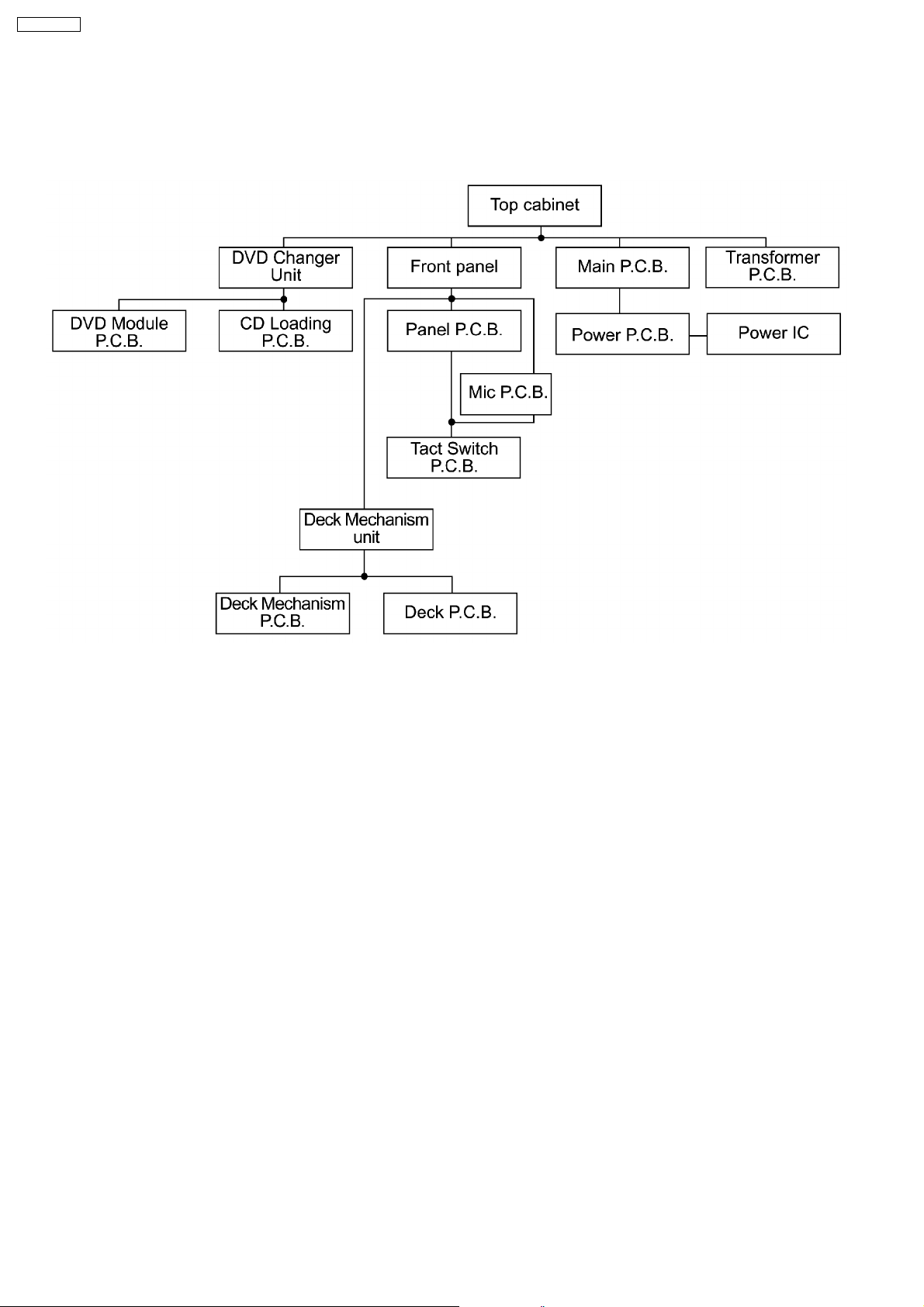
SA-VK62DEE
15.2. Disassembly flow chart
The following chart is the procedure for disassembling the casing and inside parts for internal inspection when carrying out the
servicing.
To assemble the unit, reverse the steps shown in the chart as below.
28
Page 29
15.3. Disassembly of Top Cabinet
Step 1 Remove 2 screws at each side and 5 screws at rear
panel.
Step 2 Lift up both sides of the top cabinet, push the top
cabinet towards the rear and remove the top cabinet.
SA-VK62DEE
15.4. Disassembly of Rear Panel
· Follow the (Step 1) - (Step 2) of Item 15.3 - Disassembly of Top Cabine t
Step 1 Remove 8 screws and disconnect wire CN2810 (Fan) at
rear cabinet as shown.
15.5. Disassembly of DVD Changer Unit
· Follow the (Step 1) - (Step 2) of Item 15.3 - Disassembly of Top Cabine t
Step 1 Remove one screw at rear panel.
Step 2 Detach the FFC wires (CN2801 & CN2805).
29
Page 30
SA-VK62DEE
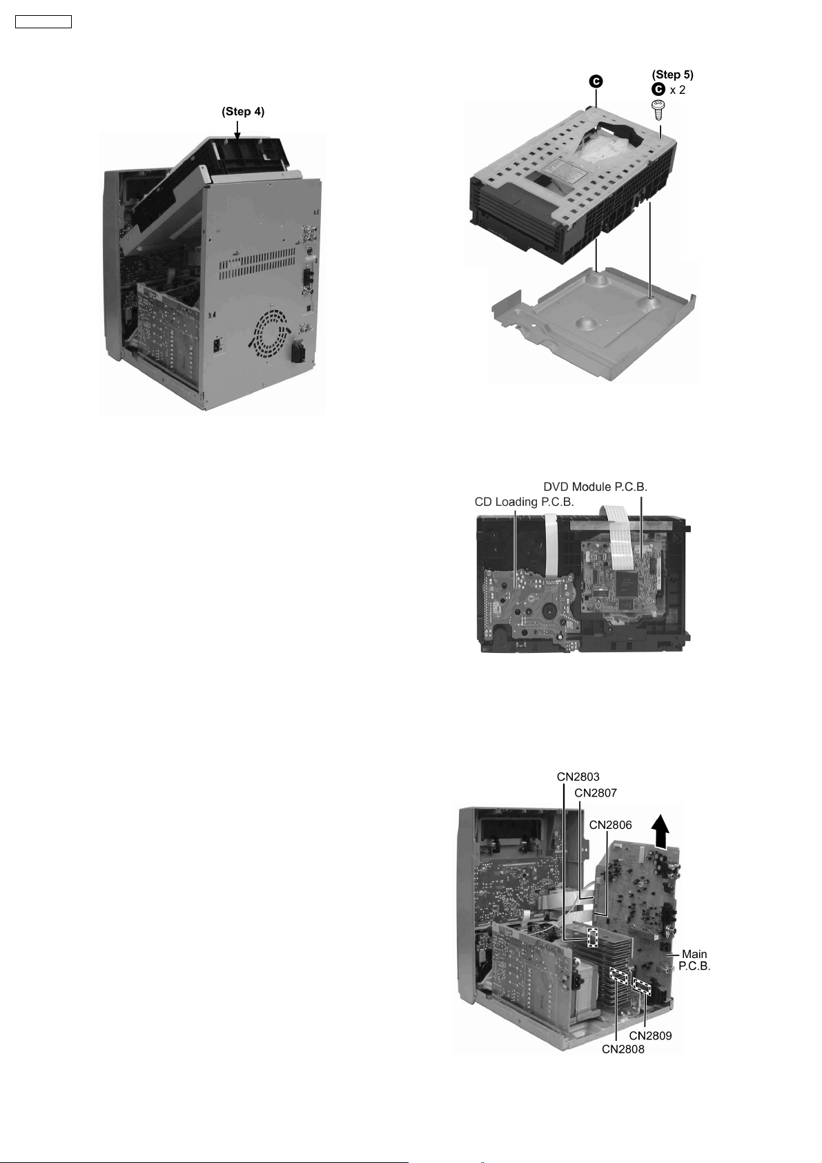
Step 3 Release the claws on both ends, and remove the DVD
changer unit.
Step 4 Lift the DVD changer unit upwards.
Step 5 Remove 2 screws.
Step 6 Remove the mechanism unit cover.
Step 7 Lay the unit.
· For disassembly of DVD mechanism unit, please refer to
Section 15.16 of this manual.
15.6. Disassembly of Main P.C.B.
· Follow the (Step 1) - (Step 2) of Item 15.3 - Disassembly of Top Cabine t
· Follow the (Step 1) of Item 15.4 - Disassembly of Rear Panel
· Follow the (Step 1) - (Step 3) of Item 15.5 - Disassembly of DVD Changer Unit
Step 1 Detach CN2810 (Fan).
Step 2 Disconnect FFC wires CN2803, CN2806 and CN2807
from Main P.C.B.
30
Page 31

SA-VK62DEE
Step 3 Lift up Main P.C.B. by disconnecting connectors
CN2808 & CN2809 as arrow shown above.
15.7. Disassembly of Power P.C.B.
· Follow the (Step 1) - (Step 2) of Item 15.3 - Disassembly of Top Cabine t
· Follow the (Step 1) of Item 15.4 - Disassembly of Rear Panel
· Follow the (Step 1) - (Step 3) of Item 15.5 - Disassembly of DVD Changer Unit
· Follow the (Step 1) - (Step 3) of Item 15.6 - Disassembly of Main P.C.B.
Step 1 Remove the 2 screws fixed at heat sink and 1 screw
fixed at Power P.C.B..
Step 2 Break the joints with a metal cutter as shown below.
Note:
Insulate the Power P.C.B. with insulation material to avoid short
circuit.
· Replacement of the Power Amplifier IC/ Voltage
Regulator
Step 1 Remove 2 screws fixed to the Power Amplifier IC
and 1 screw to Voltage Regulator.
Step 3 Unsolder the terminals of Power Amp IC, transistor
and replace the components.
Step 4 Fix back the cut portion with a screw as shown.
31
Page 32

SA-VK62DEE
15.8. Disassembly of Transformer P.C.B.
· Follow the (Step 1) - (Step 2) of Item 15.3 - Disassembly of Top Cabine t
· Follow the (Step 1) of Item 15.4 - Disassembly of Rear Panel
· Follow the (Step 1) - (Step 3) of Item 15.5 - Disassembly of DVD Changer Unit
· Follow the (Step 1) - (Step 3) of Item 15.6 - Disassembly of Main P.C.B.
· Follow the (Step 1) of Item 15.7 - Disassembly of Power P.C.B.
Step 1 Remove 3 screws, disconnect connectors W5950,
CN5950 & CN595 1.
15.9. Disassembly of Front Panel Unit
· Follow the (Step 1) - (Step 2) of Item 15.3 - Disassembly of Top Cabine t
· Follow the (Step 1) of Item 15.4 - Disassembly of Rear Panel
· Follow the (Step 1) - (Step 3) of Item 15.5 - Disassembly of DVD Changer Unit
Step 1 Lay the unit as shown below.
Step 2 Release 2 claws at bottom and 2 claws each side, draw
the front panel ass’y forward.
Step 3 Remove the volume knob.
32
Page 33

15.10. Disassembly for Panel P.C.B. & Mic P.C.B.
· Follow the (Step 1) - (Step 2) of Item 15.3 - Disassembly of Top Cabine t
· Follow the (Step 1) of Item 15.4 - Disassembly of Rear Panel
· Follow the (Step 1) - (Step 3) of Item 15.5 - Disassembly of DVD Changer Unit
· Follow the (Step 1) - (Step 3) of Item 15.9 - Disassembly of Front Panel Unit
Step 1 Remove 7 screws.
Step 2 Disconnect connectors (H6555/W6555, CN1001,
CN6806 and CN6807).
· Disasse mbly of Mic P.C.B.
SA-VK62DEE
Step 4 Remove 2 screws.
Step 5 Lift up Mic P.C.B. to remove it.
Step 3 Release 3 catches.
15.11. Disassembly for Tact Switch P.C.B.
· Follow the (Step 1) - (Step 2) of Item 15.3 - Disassembly of Top Cabine t
· Follow the (Step 1) of Item 15.4 - Disassembly of Rear Panel
· Follow the (Step 1) - (Step 3) of Item 15.5 - Disassembly of DVD Changer Unit
· Follow the (Step 1) - (Step 3) of Item 15.9 - Disassembly of Front Panel Unit
· Follow the (Step 1) - (Step 5) of Item 15.10 - Disassembly of Panel P.C.B. & Mic P.C.B.
Step 1 Remove 5 screws.
15.11.1. Disassembly of Lid
Step 1 Remove 2 screws.
Step 2 Draw Tact Switch P.C.B. forward.
Step 2 Lift the spring sideward.
Step 3 Remove Lid.
33
Page 34

SA-VK62DEE
Note: Do not misplace the spring.
15.12. Disassembly of Deck Mechanism Unit
· Follow the (Step 1) - (Step 2) of Item 15.3 - Disassembly of Top Cabine t
· Follow the (Step 1) of Item 15.4 - Disassembly of Rear Panel
· Follow the (Step 1) - (Step 6) of Item 15.5 - Disassembly of DVD Changer Unit
· Follow the (Step 1) - (Step 3) of Item 15.9 - Disassembly of Front Panel Unit
Step 1 Detach FFC wire (CN971).
Step 2 Disconnect FFC flat cable from the connector
(CN1001).
Step 3 Remove the 5 screws.
Step 4 Push the lever upward, and then open the cassette lid
ass’y (For DECK1 and DECK2).
Step 5 Tilt the cassette mechanism unit in the direction of
arrow (1), and then remove it in the direction of arrow (2).
· For replacement of Deck Mechanism P.C.B.
Step 6 Remove 3 screws.
Step 7 Unsolder the motor terminals.
Step 8 Remove Deck Mechanism P.C.B.
15.13. Replacement for Traverse Deck
· Follow the (Step 1) - (Step 2) of Item 15.3 - Disassembly of Top Cabine t
· Follow the (Step 1) of Item 15.4 - Disassembly of Rear Panel
· Follow the (Step 1) - (Step 7) of Item 15.5 - Disassembly of DVD Changer Unit
Step 1 Move ribs at both sides to the arrow direction (The
verticval rack (R) slides and the groove opens).
34
Page 35

Step 2 Remove DVD traverse deck by rotating to the arrow
direction.
15.14. Replacement for Optical Pickup Unit (DVD mechanism)
SA-VK62DEE
· Follow the (Step 1) - (Step 2) of Item 15.3 - Disassembly of Top Cabine t
· Follow the (Step 1) of Item 15.4 - Disassembly of Rear Panel
· Follow the (Step 1) - (Step 7) of Item 15.5 - Disassembly of DVD Changer Unit
· Follow the (Step 1) - (Step 2) of Item 15.13 - Replacement of Traverse Deck
Step 1 Pull out FFC.
Step 2 Widening the catch, push the pin in.
Step 3 Remove 4 pins.
Step 4 Remove the traverse deck.
Note: As floating springs (4 pieces) come off at the same time,
be careful not to lose them.
35
Page 36

SA-VK62DEE
Step 6 Remove the dvd module board and turn it over.
Step 7 Pull FFC out from the connector.
Note: Insert a short pin into FFC of the optical pickup. [See
“Notice on handling of the optical pickup”].
Step 10 Remove the catch of the drive rack, and take out the
drive rack.
Step 8 Rotate the traverse deck (B) to the arrow direction and
shift the optical pickup to the furthest backward.
Step 9 Remove 1 screw.
Step 11 Place the convex part of an optical pickup to the
concave part of a traverse base, then take out the optical
pickup.
36
Page 37

SA-VK62DEE
37
Page 38

SA-VK62DEE
15.15. Procedure for removing CD loading mechanism
1. Turn off by pressing power SW in the body.
2. Unplug AC power cord after the indication of [GOOD-BYE],
then disassemble the body.
3. Disassemble the body, and take out CD loading
mechanism.
4. Perform disassembly according to the following procedure
for disassembly.
15.16. CR16 mechanism disassembly procedure
15.16.1. Gear for servicing information
· This unit has a gear which used for checking items
(open/close of disc tray, up/down operation of traverse unit
by manually) when servicing. (For gear information, that is
described on the items for disassembly procedures.)
· For preparation of gear (for servicing), perform the
procedures as follows.
· In case of re-servicing the same set, the “gear for servicing”
may be took off becaus e it had been used. So, the “gear for
servicing” must be stored.
1. Remove the gear attached to top cover of CD loading
mechanism.
15.16.2. Replacement for the disc tray
2. Insert the hexagonal wrench (2.5mm) into the gear.
38
Page 39

SA-VK62DEE
39
Page 40

SA-VK62DEE
15.16.3. Replacement for the traverse deck
· Follow the (Step 1) - (Step 10) of item 15.16.2.
40
Page 41

15.16.4. Disassembly for CD loading unit
SA-VK62DEE
· Follow the (Step 1) - (Step 10) of item 15.16.2.
· Follow the (Step 1) - (Step 4) of item 15.16.3.
41
Page 42

SA-VK62DEE
42
Page 43

SA-VK62DEE
43
Page 44

SA-VK62DEE
15.17. CR16 mechanism assembly
procedure
The following specified greases and/or oil must be applied
when some specific parts are changed.
1. Floil grease (VFK1298) : The floil grease must be
applied to tray, tray (L) and tray (R).
2. Hanarl oil (VFK1700) : The hanarl oil must be applied to
any parts with grease other than the said parts.
44
Page 45

SA-VK62DEE
45
Page 46

SA-VK62DEE
46
Page 47

SA-VK62DEE
47
Page 48

SA-VK62DEE
48
Page 49

SA-VK62DEE
49
Page 50

SA-VK62DEE
50
Page 51

SA-VK62DEE
51
Page 52

SA-VK62DEE
52
Page 53

SA-VK62DEE
53
Page 54

SA-VK62DEE
54
Page 55

SA-VK62DEE
55
Page 56

SA-VK62DEE
15.18. Disassembly for Traverse Unit
· Follow the (Step 1) - (Step 10) of item 15.16.2
· Follow the (Step 1) - (Step 4) of item 15.16.3
56
Page 57

SA-VK62DEE
15.19. Replacement for the cassette lid ass’y
· Follow the (Step 1) - (Step 2) of Item 15.3 - Disassembly of Top Cabine t
Step 1 Lift up the lever upward, open the cassette lid ass’y.
(For DECK1 and DECK2)
Step 2 Push up the cassette lid ass’y in the direction of arrow.
(For DECK1 and DECK2).
57
Page 58

SA-VK62DEE
15.20. Rectification for tape jam problem
· Follow the (Step 1) - (Step 2) of Item 15.3 - Disassembly of Top Cabine t
Step 1 If a cassette tape cannot be removed from the deck (the
tape is caught by the capstan or pinch roller during playback or
recording), rotate the flywhe el F in the direction of the arrow to
remove it.
Step 2 Push the lever upward and open the cassette lid ass’y.
Remove the cassette tape.
58
Page 59

16 Checking for major P.C.Bs
Note:
Checking of all major P.C.Bs (Main P.C.B., Panel P.C.B., Transformer P.C.B., Deck P.C.B., Deck Mechanism P.C.B., Tact
Switch P.C.B., Mic P.C.B. and Power P.C.B.) can be carried out using below procedures.
For the disassembling procedures, refer to Section 15.
16.1. Checking of Main P.C.B.
1. Remove Top Cabinet and Rear Panel.
2. Remove CD Lid.
3. Disassemble DVD Mechanism Unit.
4. Connect FFC wires (CN2801 & CN2805) from DVD Mechanism Unit.
SA-VK62DEE
59
Page 60

SA-VK62DEE
16.2. Checking of Transformer P.C.B.
1. Remove Top Cabinet and Rear Panel.
2. Remove CD Lid.
3. Disassemble DVD Mechanism Unit.
4. Connect FFC wires (CN2801 & CN2805) from DVD Mechanism Unit.
60
Page 61

16.3. Checking of Panel, Deck & Deck Mechanism P.C.B.
1. Remove Top Cabinet.
2. Remove CD Lid.
3. Disassemble DVD Mechanism Unit.
4. Remove volume knob at Front Panel Unit.
5. Disassemble Panel P.C.B.
6. Disassemble Deck Mechanism Unit.
7. Use the extension cable (A) to reconnect (CN1001) Deck P.C.B. and (CN2803) Main P.C.B.
8. Use the extension cable (B) to reconnect (CP6401) Panel P.C.B. and (CN971) Deck Mechanism P.C.B.
SA-VK62DEE
Service Tools
Extension FFC
(A) Deck P.C.B. - Main P.C.B. REEX0485 (14 Pins)
(B) Panel P.C.B. - Deck Mechanism P.C.B. REEX0484 (10 Pins)
61
Page 62

SA-VK62DEE
16.4. Checking of Power P.C.B.
1. Remove Top Cabinet and Rear Panel.
2. Remove CD Lid.
3. Disassemble DVD Mechanism Unit.
4. Remove 3 screws at Transformer P.C.B..
5. Remove 2 screws at heat sink and 1 screw at Power P.C.B.
6. Flip the Power P.C.B.
7. Insulate the Power P.C.B. with insulation material to avoid short circuit.
8. Use the extension cable (A) to reconnect (CN1001) Deck P.C.B. and (CN2803) Main P.C.B.
9. Use the extension cable (B) to reconnect (CP6401) Panel P.C.B. and (CN971) Deck Mechanism P.C.B.
10. Use the extension cable (C) to reconnect (H5850/W5950) Power P.C.B. and (CN5950) Transformer P.C.B.
Service Tools
Extension FFC
(A) Deck P.C.B. - Main P.C.B. REEX0485 (14 Pins)
(B) Panel P.C.B. - Deck Mechanism P.C.B. REEX0484 (10 Pins)
(C) Power P.C.B. - Transformer P.C.B. RFKAK330 (9 Pins)
62
Page 63

17 Measurements and Adjustments
SA-VK62DEE
17.1. Cassette Deck Section
· Measurement Condition
−
− Reverse-mode selector switch:
− −
−
− Tape edit: NORMAL
− −
−
− Make sure head, capstan and press roller are clean.
− −
−
− Judgeable room temperature 20 ± 5 °C (68 ± 9°F)
− −
· Measuring instrument
−
− EVM (DC Electronic volmeter)
− −
−
− Digital frequency counter
− −
· Test Tape
−
− Tape speed gain adjustment (3 kHz, -10 dB);
− −
QZZCWAT
17.1.1. Head Azimuth Adjustment (Deck
1/2)
Caution:
· Please replace both azimuth adjustment screw and springs
simultaneously when readjusting the head azimuth. (shown
in Fig. 2) Even if you wish to readjust the head azimuth
without replacing the acrews and springs, a fine adjustment
to the azimuth screw and spring.
· Please remove the screw-locking bond left on the head
base when replacing the azimuth screw.
· If you wish to readjust the head azimuth, be sure to adjust
with adhering the cassette tape closely to the mechanism
by pushing the center of cassette tape with your finger.
(shown in Fig. 3)
1. Playback the azimuth adjustment portion (8 kHz, -20dB) of
the test tape (QZZCFM) in the forward play mode. Vary the
azimuth adjustment screw until the output of the R-CH (PB
OUT-R) are maximized.
2. Perform the same adjustment in the reverse play mode.
3. After the adjustment, apply screwlock to the azimuth
adjusting screw.
17.1.2. Tape Speed Adjustment (Deck 1/2)
1. Set the tape edit button to “NORMAL” position.
2. Insert the test tape (QZZCWAT) to DECK 2 and playback
(FWD side) the middle portion of it.
3. Adjust Motor VR (DECK 2) for the output value shown
below.
Adjustment target: 2940 ~ 3060 Hz (NORMAL speed)
4. After alignment, assure that the output frequency of the
DECK 1 FWD are within ±60 Hz of the value of the output
frequency of DECK 2 FWD.
Fig. 1
17.1.3. Bias Voltage Check
1. Set the unit “AUX” position.
2. Insert the Normal blank tape (QZZCRA) into DECK 2 and
the unit to “REC” mode (use “l REC/STOP” key).
3. Measure and make sure that the output is within the
standard value.
Bias voltage for Deck 2 14±4mV (Normal)
63
Fig. 2
Fig. 3
Page 64

SA-VK62DEE
17.1.4. Bias Frequency Adjustment (Deck
1/2)
1. Set the unit to “AUX” position.
2. Insert the Normal blank tape (QZZCRA) into DECK 2 and
set the unit to “REC” mode (l use “REC/STOP” key).
3. Adjust L1002 so that the output frequency is within the
standard value.
Standard Value: 89 ~ 110 kHz
17.2. Tuner Section
17.2.1. AM-IF Alignment
1. Connect the instrument as shown in Fig. 5.
2. Set the unit to AM mode.
3. Apply signal as shown in Fig. 5 from AM-SG.
4. Adjust Z2602 so that the output frequency is maximized in
Fig. 6.
Fig. 4
Fig. 5
Fig. 6
17.2.2. AM RF Adjustment
1. Connect the instrument as shown in Fig. 7.
2. Set the unit to AM mode.
3. Set AM-SG to 520kHz.
4. Receive 520kHz in the unit.
5. Adjust L2601 (OSC) so that the EVM-AC is maximized.
6. Set AM-SG to 600Hz.
7. Receive 600Hz in the unit.
8. Adjust L2601 (ANT) so that the EVM-SG is maximized.
9. Set AM-SG to 520kHz.
10. Receive 520kHz in the unit.
11. Adjust L2602 (OSC) so that the EVM-DC value is with
1.1±0.5V.
Fig. 7
64
Page 65

17.3. Alignment Points
17.3.1. Cassette Deck Section
17.3.2. Adjustment Point
SA-VK62DEE
65
Page 66

SA-VK62DEE
18 Block Diagram
OPTICAL PICKUP
B
QR8571
CONTROL
HFM
VCC
HFM
SUPPLY
SWITCH
Q8552
Q8551
OUT
LDDVD
SWITCH
SWITCH
Q8562
Q8561
LDCD
SWITCH
SWITCH
LDU
17
LD(DVD)
16
LD(CD)
15
SW
8
SUBSEL
1M
PIN(CD)
PIN(DVD)
VREF
SUB2
SUB1
13
11RF9
14
SUB1
SUB2
VREF1
6
RF
VREF2 (RF-)
FE2
FE1
7
FE1(DVD/CD)
FE2(DVD/CD)
TC
4
TC(DVD)
TD
5
TD(DVD)
TB
2
TB(DVD)
3
TA
TA(DVD)
TRACKING COIL
T-
T+
13
14
V01-
VIN3
23
V01+
9
F-
11
V02-
MUTE12
20
FOCUS COIL
F+
12
V02+
MUTE4
MUTE3
27
TRVM+
15
V04+
IC8251
C0GBG0000048
MOTOR DRIVE
VIN1
28
2
SPINDLE MOTOR UNIT
SPM+
TRVM-
16
17
V04-
V03+
VIN2
LDCNT
3
SPM-
TRV_INNER_SW
5
6
18
V03-
OPIN-
OPOUT
1
BIAS1
4
OPIN+
24
LDIN
25
BIAS2
26
TRIN
R
78
DRV3
LPC01
126
82
AD0
LPC02
143
124
134
125
130
133
110
129
123
LPC1
LPC2
DRV7
VIN9
VIN5
VIN10
127
VIN6
VREFH
111
RFINN
132
RFINP
131
VIN7
136
VIN8
VIN3
115
137
135
VIN3RF
VIN4
138
114
116
VIN2
VIN2RF
VIN4RF
MN2DS03VP1H
OSCO
OSCI
166
165
X8621
117
VIN1
IC8001
VIN1RF
76
DV2.1
148
83
DRV1
DRV8
146
79
DRV4
147
VCOF/AD4
PWM1
139
AD2
PWM0
75
DRV0
81
128
140
AD1
DRV6
VHALF
66
Page 67

Q8560
D8550
Q8550
SWITCH
SWITCH
B
IC8601
C0EBE0000384
RESET IC
SA-VK62DEE
DQ0
2,4,5,7,8,10,11,
13,42,44,45,47,
48,50,51,53
1,2,4,5,7,8,10,
11,13-15,17,18,
252,254,256
MDQ0
DQ15
MDQ15
A0
22-26,
29-35
217,220,221,223
224,226-228,230,
233,237,238
MA0
IC8051
C3ABPG000133
64 SDRAM
A11
20
234
MA11
IC8651
RFKWMH82H160
16M FLASH ROM
/WE
/CS
UDQM
BA1
LDQM
BA0
39
21
15
19
232
249
BA1
BA0
251
DQM0
240
DQM1
243
NCSM
/RAS
CLK
38
MCK
/CAS
16
17
18
244
245
248
241
NRAS
NCAS
NWE
MCKI
A16
9,10,16,17,48
21,30,31,43,45
EXADR16
A20
EXADR20
MN2DS03VP1H
A0
1-8,18-25
23-25,27,32,
33,36,37,39-42,
46,47,50,51
EXADT0
IC8001
A15
EXADT15
DV2.1
DQ0
39-36, 38-45
192-195,197-200,
203,204,206-208
210-212
MDQ16
DQ15
MDQ31
XWE
11
22
NEXWE
26
38
XRESET
XCE
28
52
NEXCE
XOE
NEXOE
12
R
Q8607
SWITCH
Q8606
SWITCH
IC8606
C0EBA0000031
RESET IC
IC8611
C3EBGC000055
16M EEPROM IC
VCC
B
SDA
SCL
5
6
73
59
60
P9
NRST
P8
67
Page 68

SA-VK62DEE
DIN1
45-47
DIN3
15(14)
8
MIXL(R)
10(9)
VOUTL(R)
FL(R)
SL(R)
20(19)
VOUT3(4)
VOUT5(6)
IC8420
C0FBBK000049
AUDIO DAC
SCK5BCK7DATA16LRCK
DSPCLK
A
TO MAIN
BLOCK
C
CNT
SW
15
16
VOUT8
VOUT7
ZERO2
MS
MC
MD
16
34
2
QR8420
MUTING
SWITCH
PY/Y/G
ZFLAG&AMUTE
PB/CB/B
PR/CR/R
Y
CMD
IECOUT
STATUS
4
IC8695
C0JBAA000346
LOGIC IC
2
1
B
QR8111
SWITCH
QR8112
SWITCH
5
IC8111
C0CBCBD00018
3.3V
REGULATOR
8
5
5
4
IC8691
C0JBAA000346
LOGIC IC
1
2
174-176
ADOUT0
169
ADOUT2
171
LRCK
170
ADOUT3
163
SRCK
DACCK
56
57
53
55
P11
P12
P13
P15
MN2DS03VP1H
IC8001
DV2.1
149
151
DAC1OUT
156
152
DAC3OUT
DAC2OUT
158
DAC5OUT
DAC4OUT
70
177
P1
IECOUT
69
P2
68
P3
68
Page 69

SA-VK62DEE
FM ANT
17
5
Q1 (RF AMP)
6
B
(FM)
Z2620
Q2
MIXER
Q3 Q4
BUFFER
OSC
CF2601 CF2602
8
Q2601
FM
IF AMP
IC2601
C1BB00000962
FM/AM IF AMP,
DET/AM OSC,
MIX/FM MPX
24
LEVEL
DET
FM
IF
1
ALC
BUFFER
AM ANT
L2601
D2602
L2602
B
RCH
22 21
23
AM
OSC
MIX
S-CURVE
AM/FM
FM
BUFFER
DET
REG
2
4
3
19
20
AM
IF
5
AM
RM AMP
AM
IF
AGC
COMP
TUNING
DRIVE
SD
6
18
DET
7
13
17
16
AM
ST
REG
9 10
8
15
PHASE
DET
VCO
FF FF
14
DECODER
STEREO
SWITCH
11
PILOT
CANCEL
PILOT
FF
DET
12
B
Z2602
AM
IFT
X2602
ST/DO
SD
16
PHASE DETECTOR
CHARGE PUMP
Q2606
TUNER
15V
SUPPLY
SWITCH
(FM)
DETECTOR
POWER ON
RESET
B
UNLOCK
UNIVERSAL
COUNTER
19
17
18
11
15
B
B
REFERENCE
DIVIDER
SWALLOW COUNTER
1/6,1/17,4 BITS
12 BITS PROGRAMMABLE
SHIFT REGISTER LATCH
10
7
1
2
DIVIDER
6
9
IC2602
C1CB00001937
PLL FREQUENCY SYNTHESIZER
C2B
I/F
8
1
X2603
20
14
12
13
5
DO
CE
2
3
DI
4
CL
ST/DO
PLLDA
PLLCLK
CE
B
69
Page 70

SA-VK62DEE
PLLDA
ST/DO
PLLCLK
SD
FL6601
P18
P1
23~40
11~14,
16~29
FL30
FL13
/RESET
/CS
SCK
9
SDATA
8
10
3
FL DISPLAY
IC6601
C0HBB0000044
FL DRIVER
RM11
UP/DOWN MOTOR
G1
G13
5~17
1~2,
30~40
FL0
FL12
XOUT
XIN
6
5
RM21
LOADING MOTOR
FROM POWER
TRANSFORMER
M M
4
OUT1
IC11
C0GAG0000007
UP/DOWN
MOTOR DRIVER
F_IN
7
2
R_IN
9
OUT2
4
C0GAG0000007
LOADING
MOTOR DRIVER
7
OUT1
IC21
F_IN
2
OUT2
R_IN
9
HALF
MODE
S951
S952
30
22
21
29
74
SD
ST/DO
PLLDA
CE
3
PLLCE
PLLCK
V_JOG_A
67
68
VR6201
JOG VOL
V_JOG_B
71
FL_CLK
72
FL_CS
FL_RESET
73
FL_DOUT
15
C2CBJG000639
X_IN
13
X2802
X_OUT
84
UP/DOWN_L
IC2801
10
83
UP/DOWN_R
MICROPROCESSOR
XC_OUT
XC_IN
11
X2801
80
OP/CL_FWD
79
OP/CL_REV
RMT
18
Z6481
REMOTE SENSOR
53
52
MODE_1
HALF_1
70
Page 71

(DECK 1)
P.B. HEAD
(DECK 2)
R/P HEAD
LCH
LCH
4
2
IC1004
C1AA00000612
R/P SELECT
(DECK 2)
ERASE HEAD
3
5
Q1003
SWITCHING
(BEAT PROOF/
RECH)
IC1001
AN7348S-E1
P.B EQ/REC AMP/
ALC/TPS AMP
24(23)
1(2)
22(3)
21(4)
17(8)
6
19
15
12
L1002
LOGIC L/H
ALC
NOR/CrO &
HI/LO LOGIC
LOGIC
REC/PB
9
B
RIPPLE
REJECTION
11
BIAS OSC
CONTROL
Q1004, Q1005,
Q1007
SA-VK62DEE
20(5)
18(7)
10
16
14
13
Q2978
SWITCH
IC951
CNB13030R2AU
PHOTO
INTERRUPTER
97
PHOTO_1
S1
STOCK
RECINH_R
S974
OPEN_SW
81
S4
Q2979
DECK
MOTOR
SWITCH
C2CBJG000639
S5
CHANGE
B
IC971
CNB13030R2AU
PHOTO
INTERRUPTER
95
PHOTO_2
CHANGE_SW
85
IC2801
MICROPROCESSOR
D6201~D6204
B
Q6415, Q6425
PLUNGER
SUPPLY SWITCH/
PLUNGER:ON/OFF
SWITCH
58
59
MTR
REC
LED1
48~51
LED4
60
56
PLG1
DECK1_H
POSITION
82
PHOTO COUPLER
Q6201~Q6204
LED
DRIVE
Q1
D951
Q6411, Q6421
PLUNGER
SUPPLY SWITCH/
PLUNGER:ON/OFF
SWITCH
57
PLG2
B
D971
Q1017
MOTOR
SWITCH
M
M1002
HALF
MODE
RECINH_F
S972
S975
S971
Z971
INTERFACE
91
DECK2
ST_SW
PLAY
PLAY_SW
87
S2
78
S3
BOTTOM
BOTTOM_SW
86
OPEN
71
Page 72

SA-VK62DEE
RED
JK2803
COMPONENT
VIDEO
MIX_L(R)
CR
12
CbOUT
2
CIN
C
BLUE
GREEN
JK2800
S.VIDEO OUT
G Y
CG
C0DAAZG00012
Y
VIDEO
CB
IC2561
REGULATOR
5
Q2552
SWITCH
IC2563
C0DBEZG00021
REGULATOR
13
CyOUT
15
VOUT
IC2701
Q2901
SWITCH
C9ZB00000466
VIDEO IC
11
CrOUT
14
YOUT
16
COUT
CyIN
CbIN
CrIN
4
YIN
6
8
9
JK2801
OPTICAL
Y
PY/PY/G
PB/CB/B
PR/CR/R
AUDIODIGITAL
DSPCLK
STATUS
CMD
B
Q2912
B
SWITCH
ZFLAG&AMUTE
A
TO DVD
BLOCK
36
4
6
37
35
DVDPCON
C2CBJG000639
WIDE1
IC2801
MICROPROCESSOR
72
DVD_MUTE
DVD_CLK
DVD_CMD
DVD_STAT
Page 73

JK6502
MIC2
JK6501
MIC1
SA-VK62DEE
7(8)
B1(2)
22(21)
JK2801
AUX
IC6550
Q6501, Q6502
Q6503
LIMITTER
Z
MIC
AMP
M65850FPCF0T
ECHO
2
10
9
IC2103
C0ABBB000067
DUAL OP-AMP
2(6)
3(5)
1(7)
13(14)
32(31)
9(10)
E1(2)
5(6)
A1(2)
IC2101
C1BB00000732
AUDIO SOUND
REC1(2)
PROCESSOR
C1(2)
2(4)
SEL1(2)
SI
SC
17
18
OUT1(2)
IC2802
C3EBDG000072
E-EPROM
(NOT SUPPLIED)
5
6
43
EE_DAT
42
4
41
EE_CLK
3
EE_CS
MICSW
Q6550
76
ECHO_MUTE
Q6504
75
ECHO_LVL3
C2CBJG000639
Q6505
Q6506
70
ECHO_LVL2
IC2801
MICROPROCESSOR
D2332
SWITCHSWITCHSWITCHSWITCH
26
69
ECHO_LVL1
1
LM_L
27
ASP_DAT
ASP_CLK
73
Page 74

SA-VK62DEE
IC2804
C0AABA000009
DUAL OP-AMP
2(6)
3(5)
Q2142 (Q2242)
Q2502
MUTING
SWITCH
Q2143 (Q2243)
MUTING
SWITCH
Q2501
MUTING
B
CONTROL
AGC
CONTROL
1(7)
FILTER
FILTER
Q2366
SWITCH
HP_L(R)
40
MUTE_A
C2CBJG000639
IC2801
MICROPROCESSOR
Q2806
POWER
RESET
CONTROL
SWITCH
12
B
/RESET/EFP_RESET
Q2701,
Q2704~Q2706
FAN
MOTOR
DRIVE
FAN
M
B
D2576
KEY1
B
B
B
B
DC_DET
HP_SW
20
39
46
SYNC
MUTE_H
Q2570
SWITCH
Q2576
SWITCH
Q2551
SWITCH
D2578
B
S6101~S6106,
S6201~S6210, S6301~S6310
DCDET
92 ~ 94
KEY3
SYNC
MUTE_H
PCONT/EFP_/CE
47
74
Page 75

SA-VK62DEE
DC_DET
FAN
HP _SW
MUTE_H
SYNC
D5813
10(14)
11(13)
12
9
-IN L(R)
+IN L(R)
IN GND
OUT GND
Q5812, Q5813
DC DETECT
SYNCHRONISING
IC5801
RSN35H2B-P
POWER HIC
FILTER
FILTER
SWITCH
Q5814
HEADPHONE
MUTING
SWITCH
Q5952
SWITCH
OUT L(R)
AC DET
LATCH
-VCCM
Q5801
10V VOLTAGE
REGULATOR
4(1)
6
5
FILTER
8
B
Q5802, Q5805
VOLTAGE SUPPLY/
CURRENT CONTROL
SWITCH
D5814
LCH
JK5851
HIGH CH
(6 W)
JK6551
HEADPHONE
RCH
Q5950
SYSTEM 6V
VOLTAGE
B
REGULATOR
Q5954
CURRENT
LIMITING
B
SWITCH
D5961~D5964
5V VOLTAGE
B
REGULATOR
Q6804
SWITCH
Q6805
SWITCH
SIGNAL LINES
: MAIN SIGNAL LINE
: FM OSC SIGNAL LINE
: FM SIGNAL LINE
( ) Indicates the Pin No. of Right Channel.
B
Q5804, Q5806, Q5807Q5808
CURRENT STABILISER/
LIMIT SWITCH/
10V VOLTAGE REGULATOR
B
Q6803
SWITCH
: CD SIGNAL LINE
: AM OSC SIGNAL LINE
: AUX SIGNAL LINE
D5969
Q5951
VOLTAGE
REGULATOR
(-VP)
FP5833
D5959
FP5950
FL DISPLAY
D5950~D5953
FP5951
TO
Q5803
15V VOLTAGE
REGULATOR
B
B
: AM SIGNAL LINE
: FM/AM SIGNAL LINE
: CD-DA (AUDIO/VIDEO) SIGNAL LINE
NOTE : Signal Lines are applicable to the Left Channel only.
T5950
POWER TRANSFORMER
Q5953
: PLAYBACK SIGNAL LINE
: RECORD SIGNAL LINE
: DVD (AUDIO) SIGNAL LINE
: DVD (VIDEO) SIGNAL LINE
RL5950
POWER
SWITCH
CONTROL
T5951
SUB
TRANSFORMER
JK5950
F1
Z5950
AC INLET
B
E5800
E5801
75
Page 76

SA-VK62DEE
19 Schematic Diagram
(All schematic diagrams may be modified at any time with the
development of the new technology)
Note:
S1 : Stock Switch
S2 : Play Switch
S3 : Bottom Switch
S4 : Open Switch
S5 : Change Switch
S951 : Mode Switch
S952 : Half Switch
S971 : Mode Switch
S972 : Half Switch
S974 : Recinh_R Switch
S975 : Recinh_F Switch
S6101 : Power Switch
S6102 : Disc Check Switch
S6103 : Multi Remaster Switch
S6104 : Surround Advanced Switch
S6105 : Deck1/2 Switch
S6106 : Rec Switch
S6201 : DVD/CD Switch
S6202 : Tape Switch
S6203 : Tuner Switch
S6204 : Aux Switch
S6205 : Deck 1 Switch
S6206 : Display Switch
S6207 : Deck 2 Switch
S6208 : Rew Switch
S6209 : FF Switch
S6210 : Stop Switch
S6301 : Open/Close Switch
S6302 : Disc Change Switch
S6303 : Disc 5 Switch
S6304 : Disc 4 Switch
S6305 : Disc 3 Switch
S6306 : Disc 2 Switch
S6307 : Disc 1 Switch
S6309 : S.SEQ Switch
S6310 : Sound EQ Switch
VR6201 : VR Volume Jog
VR6501 : VR Mic
· The voltage value and waveforms are the reference voltage
of this unit measured by DC electronic voltmeter (high
impedance) and oscilloscope on the basis of chassis.
Accordingly, there may arise some error in voltage values
and waveforms depending upon the internal impedance of
the tester or the measuring unit.
· Importance safety notice :
Components identified by
characteristics important for safety. Furthermore, special
parts which have purposes of fire-retardant (resistors), highquality sound (capacitors), low-noise (resistors), etc. are
used. When replacing any of components, be sure to use
only manufacturer´s specified parts shown in the parts list.
Caution !
IC, LSI and VLSI are sensitive to static electricity.
Secondary trouble can be prevented by taking care during
repair.
mark have special
· Cover the parts boxes made of plastics with aluminium foil.
· Put a conductive mat on the work table.
· Ground the soldering iron.
· Do not touch the pins of IC, LSI or VLSI with fingers directly .
76
Page 77

19.1. Optical Pickup Unit Circuit
SCHEMATIC DIAGRAM - 1
SA-VK62DEE
TO
HFM
PCB
TO
LDU
PCB
1
2
3
4
5
6
1
2
3
4
5
6
7
8
9
10
11
12
13
14
15
16
17
18
OPTICAL PICKUP UNIT CIRCUIT
GND
VCC
GND
GND
OUT
GND
GND
TB
TA
TC
TD
FE1
FE2
IM
RF
GND
VREF
VCC
SUB2
SUB1
SW
LD (CD)
LD (DVD)
LDGND
L4
J0JBC0000105
L3
J0JBC0000105
C8
0.1
C1
0.1
: +B SIGNAL LINE : CD-DA SIGNAL LINE
T+
26
F+
25
HFM
GND (IM)
VREF2(RF-)
PIN (DVD)
LD (CD)
LD GND
LD (DVD)
GND (OEIC)
VREF1
VCC
SUB2
SUB1
PIN(CD)
GND (IM)
FE2
FE1
SW
F-
T-
TA
TB
TD
TC
RF
24
23
22
21
20
19
18
17
16
15
14
13
12
11
10
9
8
7
6
5
4
3
2
1
TO
DVD MODULE
CIRCUIT
(FP8501) ON
SCHEMATIC
DIAGRAM - 2
TO ACT
R2
0
R4
C2
0
0.1
6.8K
R1
0
R3
0
R5
0
R6
0
R7
C3
0.1
VR1
6.8K
VR2
6.8K
C5
22PC622P
L2
J0JCC0000307
L1
J0JBC0000105
0.22
C7
0.1
C4
77
Page 78

SA-VK62DEE
19.2. DVD Module Circuit
SCHEMATIC DIAGRAM - 2
FP8201
TO
SPINDLE
MOTOR
DVD MODULE CIRCUIT
TRV_INNER_SW
1
DGND
2
TRVM+
3
TRVM-
4
SPM+
5
SPM-
6
C8251
6.3V220
C8254
0.1
R8261
82K
R8263
82K
R8264
4.7K
LB8512 ERJ3GEY0R00V
LB8513 ERJ3GEY0R00V
LB8511 ERJ3GEY0R00V
LB8514 ERJ3GEY0R00V
: +B SIGNAL LINE : CD-DA SIGNAL LINE
C8261
0.1
IC8251
C0GBG0000048
DRIVE IC
C8257
0.1
R8262
4.7K
BIAS1
1
VIN1
2
VIN2
3
4
OPIN+
OPIN-
5
OPOUT
6
GND(PRE)
7
FIN
VCC
8
MUTE12
9
GND
10
VO2-
11
VO2+
12
VO1-
13
14
VO1+
PREVCC
IC8251
LDCNT
MUTE3
TRIN
BIAS2
LDIN
VIN3
VCC
MUTE4
GND
VO3-
VO3+
VO4-
VO4+
C8262
0.1
28
27
CL8242 CL8241
26
25
CL8244 CL8243
24
23
22
FIN
3029
21
20
19
18
17
16
15
C8256
0.1
C8241
0.1
C8242
0.1
R8265
R8241
R8242
7.5K
R8251
C8253
16V22
0
22K
6.8
TL8201
C8255
0.1
R8201
2.2K
C8252
16V47
TRV-I-SW
D+5V
FODRV
TRDRV
VHALF
PNRST
MUTE3
DRV0
DRV1
M+9V
MUTE124
AD1
TO
OPTICAL
PICKUP
UNIT
CIRCUIT
ON
SCHEMATIC
DIAGRAM-1
FP8501
T+
26
F+
25
F-
24
T-
23
HFM
22
TA(DVD)
21
TB(DVD)
20
TD(DVD)
19
TC(DVD)
18
FE2(DVD/CD)
17
FE1(DVD/CD)
16
GND
15
RF
14
VREF2(RF-)
13
PIN(DVD)
12
LDCD
11
LDGND
10
LDDVD
9
GND(OEIC)
8
VREF1
7
VCC
6
SUB2
5
SUB1
4
PIN(CD)
3
SUBSEL
2
GND(VRCD)
1
C8504 0.1
RX8502
(56 x 4)
RX8504
(56 x 2)
RX8501
(56 x 2)
R8506 1.5K
LB8505 J0JCC0000119
LB8504 J0JCC0000119
LB8503 ERJ2GE0R00X
R8505 2.2K
R8501 0
RX8503
(56 x 2)
C8505
220P
C8218 1
C8217 1
C8506
100P
VIN1
VIN2
VIN4
VIN3
VIN8
VIN7
RFINP
RFINN
LPC1
VREFH
VIN6
VIN5
LPC2
RAM_CD
78
Page 79

SCHEMATIC DIAGRAM - 3
SA-VK62DEE
DVD MODULE CIRCUIT
CL8006
K8004
D8571
MA2J72800L
LB8507
J0JCC0000119
C8502
0.1
ERJ2GE0R00X
CL8012
ERJ2GE0R00X
UNR511V00L
SUPPLY CONTROL SWITCH
LB8502
J0JHC0000045
C8501
CL8002
K8009
CL8010
QR8571
10
C8561
0.1
C8112
1
CL8571
R8567
51
R8568
47K
C8113
470P
R8566
56
TL8111
: +B SIGNAL LINE
IC8111
C0CBCBD00018
3.3 REGULATOR IC
1
VO
2
NC
IC8111
3
GND
4
CN
C8563
R8563
6.3V47
R8565
2.2
Q8562
SWITCH
1K
TL8522
2SB09700RL
R8564
22
8
VIN
7
NC
6
NC
5
Cont
Q8550
2SB1219AHL
SWITCH
16V10
C8562
C8564 1
R8562
1K
C8 111
0.1
QR8112
UNR521400L
R8550
7.5K
R8560
1K
R8570
100K
R8561
0
Q8561
2SD1819A0L
SWITCH
SWITCH
C8550
6.3V33
R8569
12K
Q8560
R8112
22K
D8550
MA2J11100L
CL8561
R8 111
22K
QR8111
UNR521400L
SWITCH
L8550
G1C100KA0055
Q8560
2SD1819A0L
SWITCH
D+3.3V
D+5V
D+1.2V
HFMON
A+5V
PNRST
LPCO2
C8503
0.1
C8551
0.1
R8559
15K
R8557
51
R8558
47K
Q8552
2SB09700RL
SWITCH
R8556
56
TL8513
C8553
6.3V47
TL8512
79
R8553
1K
R8555
2.2
R8554
68
Q8551
2SD1819A0L
SWITCH
C8554 1
R8552
1K
C8552
16V10
R8551
AD0
CL8551
0
LPCO1
Page 80

SA-VK62DEE
SCHEMATIC DIAGRAM - 4
DVD MODULE CIRCUIT
Y/PY/G
CB/PB/B
CR/PR/R
Y
C
STBDAC
SBT3
SBO3
ADAC-CLK
DMIXOUT
SRCK
LRCK
VOUT4
VOUT3
AMUT
AUDIODIGITAL
A+5V
D+1.2V
M+9V
D+5V
CL8421
1
1
ZERO1
MS
2
MC
3
4
MD
IC8420
5
SCK
6
DATA
BCK
7
8
LRCK
IC8420
C0FBBK000049
2-CH DAC IC
CL8023
CL8491
C0JBAA000346
AND GATE LOGIC IC
ZERO2
VOUTL
VOUTR
VCOM
AGND
IC8691
VCC
16
15
14
13
12
11
10
NC
9
NC
C8423
6.3V33
C8424
0.1
C8428
0.1
J0JCC0000091
R8420
2.2K
LB8690
: MAIN SIGNAL LINE
: +B SIGNAL LINE
C8422
0.1
C8421
6.3V100
QR8420
UNR521100L
AUDIO MUTING SWITCH
: DVD VIDEO SIGNAL LINE
: DVD AUDIO SIGNAL LINE
LB8303 J0JCC0000119
LB8304 J0JCC0000119
LB8305 J0JCC0000119
LB8301 J0JCC0000119
LB8302
K8421 ERJ3GEY0R00V
LB8421 ERJ2GE0R00X
LB8422 ERJ2GE0R00X
LB8423 ERJ2GE0R00X
LB8424 ERJ2GE0R00X
LB8491
J0JCC0000119
ERJ2GE0R00X
FL8103
F1H0J1050022
FL8102
F1H0J1050022
FL8101
F1H0J1050022
FL8104
F1J1E1040022
ERJ2GE0R00X
K8106
VGND
Y/PY/G
VGND
CB/PB/B
VGND
CR/PR/R
VGND
VGND
ADAC5V
MIX-L
ADAC5V
MIX-R
ADACGND
ADACGND
ADACGND
ADACGND
ADACGND
CNT
ADACGND
A-REF
ZFLAG&AMUTE
DGND
AUDIODIGITAL
DGND
D+5V
DGND
D+5V
DGND
A+5V
AGND
A+5V
AGND
D+1.2V
DGND
D+1.2V
DGND
M+9V
MGND
M+9V
MGND
OP_CPU-CLK
OP_CPU-CMD
OP_CPU-STAT
Y
C
FL
FR
SL
SR
SW
FP8101
1
2
3
4
5
6
7
8
9
10
11
12
13
14
15
16
17
18
19
20
21
22
23
24
25
26
27
28
29
30
31
32
33
34
35
36
37
38
39
40
41
42
43
44
45
46
47
48
49
50
TO
MAIN CIRCUIT
(CN2801) ON
SCHEMATIC
DIAGRAM - 12
OPU_CPU-CLK
OPU_CPU-CMD
OPU_CPU-STAT
VCC
2
3
GND
IC8695
C0JBAA000346
AND GATE LOGIC IC
VCC
2
3
GND
51
C8691
0.1
4
51
C8695
0.1
4
LB8691
ERJ2GEJ101X
LB8692
ERJ2GEJ101X
LB8693
ERJ2GEJ101X
80
Page 81

SCHEMATIC DIAGRAM - 5
SA-VK62DEE
DVD MODULE CIRCUIT
IC8611
C3EBGC000055
16M EEPROM IC
(NOT SUPPLIED)
1
A0
2
A1
IC8611
3
A2
4
GND
VCC
SCL
SDA
8
C8611
0.1
7
WP
6
5
RX8021
(10K x 2)
CL8031
CL8032
R8022 10K
CL8033
R8023 47K
RX8611
(4.7K x 2)
R8611
100
CL8612
CL8611
OPU_CPU-STAT
: +B SIGNAL LINE
SCL
SDA
OPU_CPU-CLK
OPU_CPU-CMD
TRV-SW
PNRST
EXADT_15
EXADT_14
EXADT_13
EXADT_12
EXADT_11
EXADT_10
EXADT_9
EXADT_8
EXADR_19
EXADR_20
NEXWE
EXADR_18
EXADR_17
EXADT_7
EXADT_6
EXADT_5
EXADT_4
EXADT_3
EXADT_2
EXADT_1
IC8651
RFKWMH82H160
16M FLASH ROM IC
1
A15
A14
2
3
A13
A12
4
A11
5
6
A10
7
A9
8
A8
9
A19
10
A20
11
XWE
12
XRESET
13
NC
14
WP/ACC
RDY/XBSY
15
A18
16
A17
17
18
A7
19
A6
20
A5
A4
21
A3
22
23
A2
24
A1
XBYTE
DQ15/A-1
DQ14
DQ13
DQ12
DQ11
DQ10
A16
VSS
DQ7
DQ6
DQ5
DQ4
VDD
DQ3
DQ2
DQ9
DQ1
DQ8
DQ0
XOE
VSS
XCE
EXADR_16
48
47
46
FDT_15
45
FDT_7
44
FDT_14
43
FDT_6
42
FDT_13
41
FDT_5
40
FDT_12
39
FDT_4
38
37
FDT_11
36
35
FDT_10
34
33
32
31
30
29
28
27
26
EXADT_0
25
A0
FDT_3
FDT_2
FDT_9
FDT_1
FDT_8
FDT_0
C8651
0.1
C8652
0.1
81
Page 82

SA-VK62DEE
SCHEMATIC DIAGRAM - 6
DVD MODULE CIRCUIT
C8051
MDQ_0
MDQ_1
MDQ_2
MDQ_3
MDQ_4
MDQ_5
MDQ_6
MDQ_7
DQM0
NWE
NCAS
NRAS
NCSM
BA0
BA1
MA_10
MA_0
MA_1
MA_2
MA_3
C8606
3
GND
NC
4
C8052
C8053
220P
C8054
C8055
0.1
C8607
1
0.1
1
1
VDD
0.22
R8606
100K
2SD1819A0L
12
OUT
C0EBA0000031
CD
5
1
VDD
2
DQ0
3
VDDQ
4
DQ1
5
DQ2
6
VSSQ
7
DQ3
8
DQ4
9
VDDQ
10
DQ5
11
DQ6
12
VSSQ
13
DQ7
14
VDD
15
LDQM
16
/WE
/CAS
17
18
/RAS
19
/CS
20
BA0
21
BA1
22
A10/AP
23
A0
24
A1
25
A2
26
A3
27
VDD
Q8606
SWITCH
IC8606
RESET IC
IC8051
R8607
54
VSS
53
DQ15
52
VSSQ
51
DQ14
50
DQ13
49
VDDQ
48
DQ12
47
DQ11
46
VSSQ
45
DQ10
44
DQ9
43
VDDQ
42
DQ8
41
VSS
40
NC
39
UDQM
CLK
38
37
CKE
36
NC
35
A11
34
A9
33
A8
32
A7
31
A6
30
A5
29
A4
28
VSS
10K
Q8607
2SD1819A0L
SWITCH
: +B SIGNAL LINE
C8057
2200P
C8056
0.1
C8601
0.1
C0EBE0000384
C8031
0.1
MDQ_15
MDQ_14
MDQ_13
MDQ_12
MDQ_11
MDQ_10
MDQ_9
MDQ_8
DQM1
CLK
MA_11
MA_9
MA_8
MA_7
MA_6
MA_5
MA_4
IC8601
RESET IC
IC8051
C3ABPG000133
64 SDRAM IC
R8601
3
VDD
2
RESET
GND
1
RX8013
(82 x 4)
MDQ_5
MDQ_10
MDQ_4
MDQ_11
RX8012
(82 x 4)
MDQ_3
MDQ_12
MDQ_2
MDQ_13
RX8011
(82 x 4)
MDQ_1
MDQ_14
MDQ_0
MDQ_15
EXADR_20
NEXWE
EXADT_0
EXADT_4
EXADT_8
EXADT_12
EXADR_16
EXADR_18
EXADT_14
EXADT_10
EXADT_6
EXADT_2
EXADT_1
EXADT_5
EXADT_9
EXADT_13
EXADR_17
EXADR_19
EXADT_15
EXADT_11
EXADT_7
EXADT_3
STBDAC
AMUT
SBT3
1K
PNRST
SBO3
SCL
SDA
FG
R8243
10K
CL8024
CL8021
CL8022
CL8023
CL8025
CL8026
CL8027
R8021
10K
C8003
2200P
C8004
0.1
C8005
0.1
C8006
0.1
C8007
0.1
C8008
0.1
C8009
0.1
C8010
0.1
C8011
1
82
Page 83

SCHEMATIC DIAGRAM - 7
SA-VK62DEE
DVD MODULE CIRCUIT
MDQ_9
MDQ_6
RX8014
(82 x 4)
1
C8028
255
256
MDQ6
1
2
3
4
5
6
7
8
9
10
11
12
13
14
15
16
17
18
19
20
21
22
23
24
25
26
27
28
29
30
31
32
33
34
35
36
37
38
39
40
41
42
43
44
45
46
47
48
49
50
51
52
53
54
55
56
57
58
59
60
61
62
63
64
VDD33
MDQ9
MDQ5
VSS
MDQ10
MDQ4
VDD33
MDQ11
MDQ3
VSS
MDQ12
MDQ2
VDD33
MDQ13
MDQ1
MDQ14
VSS
MDQ0
MDQ15
VDD33
VSS
EXADR20
NEXWE
EXADT0
EXADT4
EXADT8
VDD12
EXADT12
VDD33
VSS
EXADR16
EXADR18
EXADT14
EXADT10
VDD33
VSS
EXADT6
EXADT2
NEXCE
EXADT1
EXADT5
EXADT9
EXADT13
EXADR17
VDD12
EXADR19
EXADT15
EXADT11
VDD33
VSS
EXADT7
EXADT3
NEXOE
P15
P14
P13
P12
P11
P10
P9
P8
P7
VDD33
MMOD
VSS
P6P5P4P3P2P1P0FGNRST
65 66 67 68 69 70 71 72 73
MDQ_8
254
MDQ8
MDQ_7
253
VSS
DQM_1
MDQ7
DQM1
VSS
NWE
DQM_0
248249250251252
DQM0
RX8015
(22 x 2)
C8027
247
VSS
NWE
VSS
74
0.1
246
75
NCAS
245
VDD33
DRV0
76
NRAS
244
NCAS
DRV1
77
24379242
NRAS
DRV2
78
MCK
DRV3
CLK
R8011 22
241
VSS
MCKI
DRV4
DRV5
80
NCSM
C8026
24082239
NCSM
DRV6
81
(82 x 4)
RX8016
2200P
238
VDD33
DRV7
83
MA_9
MA9
DRV8
MA_11
237
84
0.1
C8025
236
MA11
VDD33
MA_8
VDD12
P16
85
MA_10
235
VSS
P17
86
BA0
2348823389232
BA0
VSS
87
: +B SIGNAL LINE
BA1
MA_7
RX8017
(82 x 4)
1
C8024
231912309222993228942279522696225
BA1
VSS
MA8
MA10
VDD33
MN2DS03VP1H
MONI7
VDD12
MONI6
MONI5
MONI4
90
MA_0
MA7
MA0
IC8001
VSS
MONI3
MA_6
MA_1
1
C8023
MA6
DV2.1 IC
MONI2
2249822399222
MA1
VDD33
MONI1
MONI0
97
MA_5
MA5
AVDDD
MA_2
221
VSS
MA2
PLFIL1
AVSSD
100
MA_4
C8022
220
MA4
VREFH7
101
MA_3
0.1
219
VDD12
VREFM7
102
RX8018
(82 x 4)
218
217
VSS
VREFL7
103
104
MA3
CCAPA
216
105
C8021
0.1
215
VDD33
AVSSC
106
214
DQM2
CD ATA
107
213
VSS
DQM3
AVDDC
ANAMONI1
108
FDT_0
FDT_15
212
211
MDQ16
ANAMONI2
109
110
FD_T1
C8020
210
MDQ31
RFINN
111
0.1
209
VDD33
MDQ17
RFINP
VIN6RF
112
FDT_14
208
MDQ30
VIN5RF
113
FDT_2
207
114
FDT_13
206
MDQ18
MDQ29
VIN4RF
VIN3RF
115
205
116
FDT_3
204
VSS
MDQ19
VIN2RF
VIN1RF
117
FDT_12
1
C8019
203
MDQ28
AVDDB
118
202
VDD33
VREFH5
119
201
VSS
VREFM5
120
FDT_4
200
MDQ20
VREFL5
121
FDT_11
199
122
FDT_5
198
MDQ27
MDQ21
AVSSB
LPC1
123
FDT_10
0.1
C8018
197
196
MDQ26
LPC01
124
125
FDT_6
195
VDD33
LPC2
126
FDT_9
194
MDQ22
MDQ25
TRCDATA3
TRCDATA2
TRCDATA1
TRCDATA0
VCOF/AD4
LPC02
VREFH
127
FDT_7
193
MDQ23
MDQ24
VSS
VDD33
TRCST
TRCCLK
EXTRG1
SD ATA
EXTRG0
SCLOCK
VSS
VDD33
IECOUT
ADOUT0
ADOUT1
ADOUT2
VSS
VDD12
ADOUT3
SRCK
LRCK
EXTCK
VDD33
OSCO
OSCI
VSS
DACCK
AVSSG
AVDDG
AVSSE
AVDDE
DAC5OUT
AVSSF
DAC4OUT
COMP
IREF1
VREF
DAC3OUT
DAC2OUT
AVDDF
DAC1OUT
PWM0
PWM1
AVSSH
VREFH10
AD0
VREFL10
AVDDH
AD1
AD2
VIN1
VIN2
VIN3
VIN4
VIN5
VIN6
VIN7
VIN8
VIN9
VIN10
VHALF
128
192
191
190
189
188
187
186
185
184
183
182
181
180
179
178
177
176
175
174
173
172
171
170
169
168
167
166
165
164
163
162
161
160
159
158
157
156
155
154
153
152
151
150
149
148
147
146
145
144
143
142
141
140
139
138
137
136
135
134
133
132
131
130
129
CL8029
CL8028
OPU_CPU-CLK
KMODE
OPU_CPU-CMD
OPU_CPU-STAT
CL8030
FG
PNRST
TP8219
TP8218
TP8217
TP8216
TP8215
TP8214
CL8002
TP8220
CL8003
CL8035
CL8036
C8012
0.1
MUTE124
RAM_CD
TRV-SW
MUTE3
HFMON
DRV1
DRV0
C8013
0.1
C8207
0.1
TP8213
C8203 0.1
C8211 0.033
C8212 0.1
C8213 0.1
C8214 0.1
C8204 0.1
C8216 0.018
C8215 5600P
TP8211
TP8212
RFINN
RFINP
C8221 0.1
C8222 0.1
C8223 0.1
VIN2
VIN3
VIN4
C8224 0.1
C8205 0.1
C8225 0.1
VIN1
C8226 0.1
C8227 0.1
LPC1
LPC01
LPC2
LPC02
VREFH
C8229
VHALF
1
83
Page 84

SA-VK62DEE
FDT_8
CL8040
SCHEMATIC DIAGRAM - 8
DVD MODULE CIRCUIT
LB8001
J0JHC0000045
C8002
4V330
C8017
0.1
R8041
33
K8031
ERJ2GE0R00X
6.3V100
CKA1
C8001
LB8002
J0JHC0000045
RX8031
(4.7K x 2)
: CD-DA SIGNAL LINE
: +B SIGNAL LINE
: DVD VIDEO SIGNAL LINE
: DVD AUDIO SIGNAL LINE
D+3.3V
D+1.2V
RX8032
(4.7K x 2)
CL8034
KMODE
C8307 0.1
C8312 1
C8208 0.1
C8228
1
R8401
C8014
R8315 6.8
C8234 0.1
C8232 0.1
VIN1
VIN2
VIN3
VIN4
VIN5
VIN6
VIN7
VIN8
VIN5
VIN6
C8016 1
R8404 100
C8015 1
R8402 100
47K
0.1
LB8401
ERJ2GEJ151X
C8303 0.1
C8233
4700P
C8201
6.3V100
C8308
15P
CL8233
CL8235
C8235
1000P
CL8236
C8237
1000P
CL8234
CL8231
CL8206
C8202
6.3V100
RX8401
(100 x 2)
R8233
15K
R8621
1M
C8304 1
R8235
8.2K
C8236
1000P
R8236
8.2K
C8238
820P
D8231
MA2J11100L
R8622
R8231
C8206
10K
1
270
X8621
H0J270500085
R8312 1KR8313 24K R8314 0
R8311 2.4K
C8311 0.1
C8622 12P
C8621 12P
C8302
6.3V33
L8202
J0JCC0000079
L8201
G1C100K00020
J0JCC0000079
C8301
6.3V220
R8421
0
L8302
G1C100KA0055
L8301
R8325
160
R8326
R8341
82
AUDIODIGITAL
DMIXOUT
SRCK
LRCK
ADAC-CLK
C
Y
R8321
160
0
R8322
10
D+3.3V
CR/PR/R
CB/PB/B
R8335
82
Y/PY/G
R8331
160
R8332
10
TRDRV
AD0
FODRV
AD1
D+3.3V
84
Page 85

19.3. (A) Main (Tuner) Circuit
6
SA-VK62DEE
FM EXT
ANT
75 OHM
GND
AM LOOP ANT
AM EXT
ANT
JK2601
SCHEMATIC DIAGRAM - 9
MAIN (TUNER) CIRCUIT
TUNER PACK CIRCUIT
1
1
2
2
3
3
4
4
5
5.6P 2SK544
2.7K
L2601
G2A411C00001
R2610
C2607
1K
0.047
100K
100K
D2602
B0CDBB000015
1000P
2.2P
G2BPC0000016
R2612
100K
4.7P
L2602
: +B SIGNAL LINE
: FM/AM SIGNAL LINE
2.2P
2SC2786M
1.2U
3.3P
180P
C2636
1000P
560K
680K
390
2SC1675l1l2
100K
220
18P
1000P
680K
2.2P
2SC2787FL1TA
390
390
LA1833NMNTLM
DET/AM OSC MIX/FM MPX
C2608
8P
R2619
3.3K
0.47U
5.6P
FM/AM IF AMP
R2618
3.3K
C2614
50V3.3
IC2601
J0B1075AA014
7
6
8
CF2601
1
2
C2601
0.01
C2609
1000P
OSC OUT
3
2324
OSC
: FM SIGNAL LINE
: FM OSC SIGNAL LINE
R2604
1K
C2603
R2607
0.01
330
J0B1075AA014
R2601
R2606
C2604
1000P
R2605
470
470K
0
Q2601
B1AABC000003
R2603
C2602
270
16V10
C2619
680P
R2620
47K
0.033
C2616
C2615
50V4.7
150P
2122
AFC
AGC
AM OUT
AM RF IN
IC2601
DET OUT
CF2602
1
2
Q2601
FM IF AMP
R2621
22K
R2643
22K
C2639
R2602
C2631
PILOT IN
50V4.7
: AM SIGNAL LINE
: AM OSC SIGNAL LINE
3
C2638
0.01
C2618
R2623
PILOT OUT
0.01
68K
RCH
B1GCCFJJ0016
C2620
16V10
4.7K
3300P
C2637
16101511141213
MPX IN
Q2606
TUNER 15V
SUPPLY SWITCH
R2646
100K
C2617
0.01
R2642
6.8K
C2642
R2641
50V1
6.8K
C2641
50V1
R2645
100K
C2643
6800P
LCH
Q2606
C2644
6800P
D2601
B0BC5R000009
R2614
5.6K
C2610
0.01
R2652
0
C2633
12P
X2603
H0H720400007
C2634
12P
C2630
6.3V100
C2612
0.01
R2638
3.3K
R2630
10K
20
1
XOUT
XIN
10K
R2613
C2632
C2611
1000P
50V4.7
560
R2615
R2616
19
18
17516
AIN
VSS
AOUT
LC72131MDTRM
PLL FREQUENCY SYNTHESIZER
CL
DI
CE
2
4
3
R2636 1K
R2637 1K
R2635 1K
CE
PLLCLK
PLLDA
R2611
390
C2625
16V22
1K
PD
IC2602
DO
R2634 470
DO/ST
R2651
15714
VDD
AM
6
FM DET
REG
AM MIX OUT
R2632
10K
C2606
0.01
AM IF IN
4
C2629
6.3V100
R2633
1K
FM IF IN
1234
C2627
C2626
16V22
2
1
G2BAD0000003
R2617
47K
1000P
C2613
82
13
FMIN
AMIN
MONO
LW
STRQ
SDC
8
91210
Z2602
11
FM
IFIN
1
3
56
R2628
82
R2629 27K
C2624
100P
ST
SD
GND
5206197188179
C2647
1000P
C2648
0.01
R2626
1K
R2625
X2602
W2919
DO/ST
SD
VCC
33
R2624
470
H3F1065A0002
C2649
0.1
0
STRQ
470
R2627
FM/AM
C2622
R2622
MONO
50V1
2.7K
C2621
50V0.47
C2623
50V1
R2644
120
R2631
120
RCH
LCH
PLLDA
DO/ST
PLLCLK
TGND
DO/ST
+7.5V
CE
15V
SD
A
B
C
D
TO
MAIN
E
CIRCUIT
F
(2A) ON
G
SCHEMATIC
DIAGRAM - 1
H
I
J
K
1A
85
Page 86

SA-VK62DEE
19.4. (B) Main Circuit
SCHEMATIC DIAGRAM - 10
MAIN CIRCUIT
: +B SIGNAL LINE
: PLAYBACK SIGNAL LINE
: RECORD SIGNAL LINE
: AUX SIGNAL LINE
TO
DECK
CIRCUIT
(CN1001) ON
SCHEMATIC
DIAGRAM - 21
AUX
TO
CD LOADING
CIRCUIT
(CN1) ON
SCHEMATIC
DIAGRAM - 23
CN2803
RCH
LCH
JK2802
CN2805
CR02
1
MOTOR
2
3
DECK1_H
4
5
MOGND
6
MOT+B
7
REC_H
8
+15V
9
RECINR
10
RECINL
11
AFGND
12
PBR
13
PBL
14
PLAY_SW
14
ST_SW
13
OP/CL_REV
12
OP/CL_FWD
11
OPEN_SW
10
SW5V
9
POSITION
8
BOTTOM
7
UP/DOWN_R
6
UP/DOWN_F
5
P_GND
4
CHANGE_SW
3
LOAD_GND
2
+7.5V
1
W2918 0
C2026
0.22
W2968
C2027
0.22
0
W2805 0
Q2978
B1GDCFJJ0047
SWITCH
Q2978
C2028
0.1
W2518
R2216
0
12K
C2216
680P
C2116
680P
R2116
12K
R2931 0
R2932 0
R2933 0
R2934 0
R2935 0
R2936 0
R2937 0
R2938 0
R2939 0
R2940 0
R2943 0
R2941 0
R2942 0
D2731
B0EAKM000117
R2976 0
C2976
16V10
J0JCC0000120
J0JCC0000120
C2217
100P
C2117
100P
K2111
K2211
R2217
2.7K
R2117
2.7K
/REC
+15V
REC_RIN
REC_LIN
PBR
PBL
AUXR
W2969
0
AUXL
PLAY_SW
ST_SW
OP_CL_REV
OP_CL_FWD
OPEN_SW
SW5V
POSITION
BOTTOM_SW
UP/DOWN_R
UP/DOWN_F
CHG_SW
CD8V
MOT10V
SW5V
B1GDCFJJ0047
DECK MOTOR SWITCH
DECK1_H
Q2979
R2977
/MTR
0
86
Page 87

SCHEMATIC DIAGRAM - 11
SA-VK62DEE
MAIN CIRCUIT
C2520
0.01
C2301
10P
+9V
R2149
2.2K
R2146
C2401
10P
R2403
C2402
220K
47P
7
8
IC2804
C0AABA000009
DUAL OP-AMP
2
1
364
C2302
R2303
47P
220K
R2302
12K
0
R2531
B0ACCK000005
1K
R2402
12K
R2532
0
5
C2521
0.01
W2929
D2241
0
: +B SIGNAL LINE
: -B SIGNAL LINE
C2245
R2247
16V10
100K
R2248
4.7K
R2249
2.2K
Q2142
B1GDCFJJ0047
C2151
16V10
R2153
R2253
C2251
16V10
R2246
1K
Q2242
Q2142,Q2242
B1ABCF000176
AGC CONTROL
R2145
10K
Q2501
MUTING CONTROL
R2150
0
R2152
680
1.5K
1.5K
Q2143
W2928
R2252
680
Q2243
Q2143, 2243
B1ABEB000002
MUTING CONTROL
: MIC SIGNAL LINE
: MAIN SIGNAL LINE
R2245
10K
R2154
100K
0
R2254
100K
C2242
R2243
100K
R2501
2.2K
R2272
R2172
560
B1GFGCAA0001
1
Q2502
6
R2242
1.5K
5
4
C2142
R2502
56K
560
1
5
2
3
Q2366
MUTING CONTROL
R2241
2.7K
6
4
C2241
1
1
R2142
1.5K
2
R2143
100K
3
1
C2501
N
50V2.2
R2171
3.3K
R2271
3.3K
Q2502
B1GFGCAA0001
MUTING SWITCH
R2141
C2141
2.7K
1
R2503
27K
R2191
K2408
0
R216722R2166
C2166
1000P
R216922R2168
R226922R2268
C2266
1000P
R226722R2266
R2291
K2409
0
0
0
22
R2170
22
0
R2270
0
22
22
K2406
0
0
1
C2294
1
R2297
0
0
R2197
C2194
K2407
OUT2
OUT1
-9V
MUTE_A
HI_L
HP_L
HP_R
HI_R
R2001
0
SYS6V
PCONT
R2002 0
24
23
-9V
SYNC
SW5V
R2003 0
DGND
22
20
21
VREF+
19
18
RMT
KEY1
KEY2
PHOTO1
PHOTO2
16
14
15
17
TO
PANEL CIRCUIT
(CN6807) ON
SCHEMATIC
DIAGRAM - 19
KEY3
13
DECK2
12
11
FL_CLK
FL_DOUT
10
9
FL_CS
8
FL_RST
V_JOG_B
6
7
ECHO_1
ECHO_2
V_JOG_A
W2941 0
W2942 0
4
3
5
ECHO_3
ECHO_MUTE
2
1
CN2807
87
MOT10V
PGND
MOT10V
18
19
PLG2
PLG2
17
PLG1
PLG1
16
MODE_1
MODE_PB
15
HP_L
HP_R
HALF_1
HP_R
HALF_PB
HP_GND
HP_L
14
13
11
12
TO
PANEL CIRCUIT
(CN6806) ON
SCHEMATIC
DIAGRAM - 19
LED4
LED3
LED2
R2004 0
R2008 0
R2005 0
LED4
LED3
LED2
10
9
LED1
R2009 0
LED1
8
7
+9V
MIC
R2007 0
MIC
MIC_GND
+9V
4
6
5
DVREF+
R20060C2004
DVREF+
1
3
2
0.1
CN2806
Page 88

SA-VK62DEE
SCHEMATIC DIAGRAM - 12
MAIN CIRCUIT
: +B SIGNAL LINE
: MAIN SIGNAL LINE
: DVD VIDEO SIGNAL LINE
L2912
G0A100G00005
C2977
6.3V47
R2559
3.9K
C2555
1
D2552
R2558
330
R2557
1K
B0BC7R500001
R2552 1
R2551 1
L2551
G0A101G00022
C2552
6.3V1000
R2554 1
R2553 1
D2553
R2555 1
IC2561
C0DAAZG00012
DC-DC CONVERTER
Vin Vout COM 0adj Vsoft
2345
1
C2550
25V330
B0JCPD000025
R2556
1K
Q2551
C2551
100P
R2560
10K
R2568
1K
D2551
B0ACCK000005
C2916
0.01
C2917
0.01
50V22
C2913
C2915
0.01
R2951
C2914
47K
0.01
C2925
0.1
C2927
1
C2912
0.01
B1GBCFJN0033
MUTING SWITCH
C2911
10V220
Q2912
IC2701
C9ZB00000466
VIDEO BUFFER IC
VCC2
1
CIN
2
3
BIAS
4
YIN
VCC1
5
CYIN
6
GND1
7
CbIN
8
R2913
10K
DVD_MUTE
COUT
VOUT
YOUT
CYOUT
CbOUT
CrOUT
GND2
CrIN
Q2551
B1ADCF000001
CURRENT LIMITER
16
15
14
13
12
11
10
9
C2926
50V1
C2918 0.01
C2919 6.3V100
C2920 6.3V100
C2922 6.3V100
C2923 6.3V100
C2924 6.3V100
W2996
0
W2997
0
K2411
ERJ3GEY0R00V
W2989
0
R2987
0
L2905
J0JBC0000019
DVD_PCON
VGND
50
PY/Y/G
49
VGND
48
VGND
CB/PB/B
46
47
VGND
VGND
CR/PR/RYC
44
42
45
43
41
DVD_MIXL
ADAC5V
MIXL
40
39
DVD_MIXR
ADAC5V
MIXR
38
37
R2924 0
R2923 0
ADACGNDFLADACGND
FR
34
35
36
33
R2925 0
R2926 0
R2927 0
ADACGND
ADACGND
ADACGND
SL
SR
32
CENTER
29
27
28
31
30
TO
DVD MODULE CIRCUIT
(FP8101) ON
SCHEMATIC
DIAGRAM - 4
R2928 0
ADACGND
SUBW
25
26
MOT9V
DVD_CLK
DVD_CMD
DVD_STAT
C2907
0.01
ZFLAG
DGND
DGND
DGND
DGND
DGND
AUDIODIGITAL
D+5V
22
24
23
D+5V
20
21
19
18
17
DGND
A+5V
A+5V
D+1.2V
DGND
DGND
D+1.2V
M+9V
MGND
M+9V
MGND
DSPCLK
CMD
16
12
13
11
14
15
6
10
9
8
7
STATUS
4
3
2
1
5
L2904
1
OUT
OPTICAL
C2905
0.01
C2906
16V10
J0JBC0000019
2
3
GND
VCC
JK2801CN2801
TO
TRANSFORMER
CIRCUIT
(W5950) ON
SCHEMATIC
DIAGRAM - 23
1
3
2
CN2814
88
Page 89

SCHEMATIC DIAGRAM - 13
SA-VK62DEE
MAIN CIRCUIT
Q2552
B1ACKD000005
REGULATOR
Q2552
C2553
6.3V100
W2932
0
C2554
0.01
R2563
39K
R2562
2.2K
B0EAKM000117
C2562
6.3V470
D2555 - 2557
: +B SIGNAL LINE
: -B SIGNAL LINE
R2567
D2557D2556D2555
680
C2559
6.3V470
: DVD VIDEO SIGNAL LINE
IC2563
C0DBEZG00021
REGULATOR IC
ADJ PVCC GND VO VCC GND
2
45
3
1
R2565
R2566
C2557
2.2K
1K
1
C2558
1
6
W29810W29790W2980
0
W2993
W2995
0
0
R2912
2.2K
R2914
R2908
100K
R2907
100K
R2903
75
10K
R290175R2915
L2901
C2904
470P
J0JCC0000120
J0JCC0000120
C2933
0.1
10K
R2906
C2910
470P
R2922
75
L2908
J0JCC0000120
L2903
J0JCC0000120
C2903
C2931
C2930
10K
10K
R2921
R2920
75
R2909
L2906
JK2803 JK2800
75
R2910
C2908
470P
J0JCC0000120
C2932
CB L CR R L Y R
RED BLUE GREENVIDEO
L2907
C2909
470P
0.1
0.1
0.1
0.1
R2902
75
L2902
C2902
470P
J0JCC0000120
C2901
470P
1
4
G
Y
5
C
2
3
S-VIDEO
10K
WIDE_1
B1GBCFJN0033
R2911
0
Q2901
SWITCH
R2576
4.7K
R2577
39K
+9V
B1GBCFJA0028
R2578
15K
-9V
SW5V
Q2576
DETECT SWITCH
C2576
50V4.7
D2576
B0ADCJ000020
D2578
B0ACCK000005
D2911
B0ACCK000005
MOT10V
MOT9V
R2579
47K
VREF+
DC_DET
89
Page 90

SA-VK62DEE
SCHEMATIC DIAGRAM - 14
C2335
1500P
R2314
10K
R2315
8.2K
MAIN CIRCUIT
MIC
SEL1
C2315
1
R2313
68K
R2414
10K
R2415
8.2K
SEL2
C2415
1
R2413
68K
R2412
56K
C2413
12P
C2414
47P
364
IC2103
C0ABBB000067
DUAL OP-AMP
78
5
C2313
12P
C2314
47P
R2312
56K
R2319
5.6K
VIN2
12
VIN1
R2339
R2439
C2587
0.01
C2586
0.01
1K
1K
: +B SIGNAL LINE
: -B SIGNAL LINE
+9V
W2930
0
R2591
330K
R2331
0
C2331
1
R2592
R2332
0
22K
R2419
5.6K
D2411
B0BC4R300002
D2311
B0BC4R300002
R2320
1K
R2420
1K
: MIC SIGNAL LINE
: MAIN SIGNAL LINE
-9V
D2332
B0ADCC000002
R2333
0
LM_L
R2338
1K
R2337
C2334
470K
R2715
10K
C2708
16V100
D2705
B0ACCK000005
R2714
120K
Q2705
D2704
B0ACCK000005
R2710
220K
R2707
DCDET
0.22
1K
Q2706
2SD0601AHL
DETECT SWITCH
Q2705
2SB0709AHL
SWITCH
R2713
100K
R2711
100
D2703
B0ACCK000005
C2707
10V10
N
R2712
22
TO FAN UNIT
2
1
C2705
16V10
CN2810
R2704
0
W2940
0
R2571
R2570
MOT10V
R2702
3.3K
R2717
0
-9V
Q2701
Q2570
B1AAKD000009
R2720
MOTOR SUPPLY SWITCH
27
C2570
R2572
470
680
0.01
150
C2571
25V100
R2573
0
R2705
2.2K
Q2704
R2708
R2709
10K
100K
Q2704
2SB0709AHL
FAN MOTOR DRIVE
R2706
2.2K
C2706
0.01
C2701
Q2701
2SD0592ARA
FAN MOTOR DRIVE
0.01
R2701
2.2M
FAN
90
Page 91

SCHEMATIC DIAGRAM - 15
SA-VK62DEE
DVREF+
R2854 4.7K
R2869 4.7K
R2870 4.7K
R2871 4.7K
R2872 4.7K
R2873 4.7K
OPEN_SW
POSITION
UP_DOWN_R
UP_DOWN_F
CHG_SW
BOTTOM_SW
PLAY_SW
DECK2
KEY3
KEY2
KEY1
PHOTO_2
PHOTO_1
VREF+
VCC
MAIN CIRCUIT
W2958
0
R2863 100
R2858 100
R2859 100
R2860 100
R2861 100
R2862
100
W2961 0
100P
C2817
C2864 100P
C2863 100P
C2865 100P
R2874
15K
100P
100P
100P
C2814
C2816
C2815
C2862 100P
C2861 100P
C2860 100P
R2838 1K
R2839 1K
R2840 1K
R2849 1K
R2850 1K
R2851 1K
R2852 1K
R2875
10K
W2962
0
100P
C2813
OPEN_SW
81
POSITION
82
UP/DOWN_R
83
UP/DOWN_L
84
CHG_SW
85
BOTTOM_SW
86
PLAY_SW
87
NC
88
89
DVD_REG
NC
90
DECK2
91
KEY3
92
KEY2
93
KEY1
94
PHOTO_2
95
AVSS
96
PHOTO_1
97
VREF
98
AVCC
99
NC
100
C2821 100P
C2820 100P
C2819 100P
C2818 100P
ST_SW
OP_CL_REV
OP_CL_FWD
R2835 1K
R2837 1K
R2836 1K
80
79
FWD
OP/CL_
ST_SW
OP/CL_REV
NC
PLLCE
LM_1
1
3
2
: +B SIGNAL LINE
FL_CS
FL_CLK
ECHO_3
FL_DOUT
ECHO_MUTE
76
72
73
7475
7778
FL_CLK
HP_MUTE
FL_DOUT
ECHO_LVL3
ECHO_MUTE
DVD_PCON
DVD_MUTE
NC
BYTE
WIDE1
6
4
R2856 1K
5
8
7
R2801
10K
R2894 1K
R2895 100
9
FL_RST
ECHO_1
ECHO_2
V_JOG_B
V_JOG_A
68
697071
67
FL_CS
CNVSS/EFP_CNVSS
10
V_JOG_A
V_JOG_B
/FL_RESET
ECHO_LVL1
ECHO_LVL2
IC2801
C2CBJG000639
MICROPROCESSOR
VSS
XC_OUT
XC_IN
/RESET/EFP_RESET
X_OUT
1413
12
11
VCC
/REC
PLG1
/MTR
PLG2
DECK1_H
R2846 4.7K
R2844 10K
66
65
64
NC
NC
VSS
X_IN
VCC
/NMI
16
15
17
R2802
R2845 10K
58
56
60
59
62
63
61
57
NC
NC
VCC
REC
MTR
PLG1
PLG2
DECK1_H
NC
NC
NC
ST/DO
10K
R2803
SD
W2964
0
NC
2524232221
RMT
SYNC
18
2019
100
MODE_1
R2842 10K
54
55
53
NC
NC
EE_CS/EFP_/EPM
REG4/EFP_BUSY
ASP_DAT
ASP_CLK
0
W2807
LED4
HALF_1
R2841 10K
51
52
LED4
HALF_1
MODE_1
LED3
LED2
LED1
DCDET
PCONT/EFP_/CE
EE_DAT
EE_CLK
MUTE_A
MUTE_H
DVD_CLK
DVD_STA
DVD_CMD
REG3/EFP_SCLK
REG2/EFP_RxD1
REG1/EFP_TxD1
PLL_CLK
PLL_DATA
NC
3029282726
0
W2806
50
49
48
47
46
45
NC
44
NC
43
42
41
40
39
38
NC
37
36
35
34
33
32
31
R2804 47K
R2805 47K
R2807 10K
R2806 10K
W2909
0
R2827 10K
100K
100K
R2818
R2817
R2834
1K
R2890
0
100K
C2866 100P
R2819
R2889 1K
R2888 1K
R2887 1K
W2911 0
C2867 100P
C2868 100P
VREF+
LED3
R2831 10K
LED2
LED1
DCDET
PCONT
EE_DAT
EE_CLK
EE_CS
MUTE_A
MUTE_H
DVD_CLK
DVD_STAT
DVD_CMD
BUSY
CLK
RXD
TXD
1.8K
100K
R2978
R2822
SW5V
C2831 0.022
C2832 330P
R2876 22K
R2877 22K
C2833
330P
EE_CS
VREF+
EE_CLK
2
3
4
IC2802
C3EBEG000072
E-EPROM IC
(NOT SUPPLIED)
6
5
7
R2878
4.7K
LM_L
PLLCE
WIDE_1
EE_DAT
1
8
DVD_PCON
DVD_MUTE
CNVSS
XC_IN
/RESET
X_OUT
XC_OUT
R2883 330K
R2882
10M
XIN
X2801
VCC
H0A327200115
C2840
18P
C2841
18P
RMT
R2886
1M
C2838
68P
SYNC
DO/ST
SD
R2881
220
X2802
H2B100500004
IN OUT
GND
ASP_DAT
ASP_CLK
C2856
C2834
68P
PLLCLK
PLLDA
C2852
16V100
Q2806
1
B1GBCFJJ0051
POWER RESET
CONTROL SWITCH
C2851
0.1
R2891 47K
R2810 22K
C2853
0.1
Q2806
R2892
50V2.2
C2858
0.01
D2804
B0ACCK000005
0
C2854
16V100
C2857
B0ADCJ000020
D2801
R2811
0
B0ACCK000005
D2802
SYS6V
VREF+
91
Page 92

SA-VK62DEE
SCHEMATIC DIAGRAM - 16
MAIN CIRCUIT
: +B SIGNAL LINE
: -B SIGNAL LINE
:FM/AM SIGNAL LINE
: AUX SIGNAL LINE
: MAIN SIGNAL LINE
: TAPE PLAYBACK SIGNAL LINE
: TAPE RECORD SIGNAL LINE
C2101
1
R2111
10K
R2112
22K
C2112
1000P
DVD_MIXL
PBL
C2111
0.1
DVD_MIXR
R2101
3.3K
R2201
3.3K
R2102
1.2K
C2201
1
R2212
C2118
0.1
R2211
10K
22K
C2212
1000P
R2202
1.2K
AUXL
PBR
C2119
1000P
C2211
0.1
C2102
0.1
C2202
0.1
C2103
1000P
C2218
0.1
SEL2
AUXR
SEL1
C2411
0.15
C2203
1000P
C2219
1000P
C2311
0.15
C2581
16V100
C2412
0.15
C2312
0.15
VIN1
1
2
SEL1
VIN2
3
SEL2
4
A1(L)
5
A2(R)
6
B1(L)
7
8
B2(R)
C1(L)
9
10
C2(R)
C2114
0.01
11
D1
C2214
0.01
12
D2
13
E1(L)
E2(R)
14
FILTER
15
N
16
GND
C1BB00000732
AUDIO SOUND PROCESSOR
C2584
220P
C2120
1
C2220
IC2101
IC2101
R2584
R2318 2.7K
R2418 2.7K
1
MOUT1
MOUT2
BOUT1
BOUT2
330K
SW5V
REC1
REC2
MNF1
MNF2
BNF1
BNF2
OUT1
OUT2
CAP
VCC
R2317
100K
R2417
SI
SC
R2586
1.2K
100K
32
31
30
29
28
27
26
25
24
23
22
21
20
19
18
17
C2207 0.1
C2208
1000P
R2220 1K
R2120 1K
C2107
0.1
C2108
1000P
R2316
8.2K
R2416
8.2K
C2121
0.1
C2221
0.1
C2126
0.1
C2226
0.1
C2131
0.22
C2231
0.1
C2136
0.22
C2236
0.1
C2583
0.22
C2585
220P
ASP_CLK
R2207
47K
R2107
47K
R2103
8.2K
R2108
8.2K
R2113
8.2K
R2118
8.2K
R2585
330K
R2587
1.2K
C2588
0.1
C2206
3300P
C2106
3300P
ASP_DAT
R2206
R2106
C2582
16V100
100
100
R2582
0
/RESET
CNVSS
VCC
BUSY
REC_LIN
REC_RIN
VIN2
VIN1
OUT1
OUT2
+9V
W2912
W2926
0
R2033
4.7K
W2925
0
R2031
27
0
W2922
W2924
C2031
0.01
0
0
R2021 2.2K
CLK
RXD
TXD
PLLCE
PLLDA
PLLCLK
+15V
DO/ST
SD
+9V
FAN
DC_DET
MUTE_H
+15V +15V
HI_L
HI_R
CD8V
MOT10V
+9V
-9V
SW5V
/RESET
CNVSS
C2032
0.01
R2032
10K
D2031
B0BC7R500001
DC_DET
MUTE_H
HIGH_LIN
HIGH_RIN
A_GND
FL_GND
UP GND
MOT10V
C2021
16V100
VCC
BUSY
EFM
CLK
RXD
TXD
PLLDA
DO/ST
PLLCLK
DO/ST
FAN
T GND
P_GND
CD8V
+9V
-9V
SW5V
RCH
CE
LCH
TGND
+15V
+7.5V
SD
1
2
3
FOR
4
MICRO-P
5
UPDATE
6
7
8
CN2811
A
B
C
D
E
F
G
H
I
J
K
(2A)
1
2
3
4
TO
5
POWER
6
CIRCUIT
(CN5800) ON
7
SCHEMATIC
8
DIAGRAM - 22
9
10
11
12
CN2809
1
2
3
TO
4
POWER
5
CIRCUIT
6
(CN5801) ON
7
SCHEMATIC
8
DIAGRAM - 22
9
10
11
12
CN2808
TO
MAIN (TUNER)
CIRCUIT
(1A) ON
SCHEMATIC
DIAGRAM - 9
92
Page 93

19.5. (C) Panel Circuit , (D) Tact Switch Circuit & (E) Mic Circuit
SCHEMATIC DIAGRAM - 17
: +B SIGNAL LINE
PANEL CIRCUIT
D6102
D6101, 6102
B3AAA0000583
D6101
S6101
POWER
S6102
DISC CHECK
S6103
MULTI
REMASTER
S6104
SURR
ADVANCED
S6105
DECK 1/2
S6106
REC
+9V
MIC
MIC_OUT
R6109
2.7K
R6108
2.7K
R6107
R6101
R6102
R6103
R6104
R6105
R6106
10K
1.2K
1.8K
2.2K
2.7K
: -B SIGNAL LINE
SYS6V
VREF+
FL1
G1G2G3G4G5G6G7G8G9
KEY1
FL1
1K
1K
1
C6631
35V22
FL_CS
56
FL00
7
FL01
FL02
SW5V
FL_RESET
FL_CLK
FL_DOUT
: MIC SIGNAL LINE
FL6602
A2BD00000124
FL DISPLAY
G11
G12
G13NCNCNCNCNCP1P2P3P4P5P6P7P8P9
FL09
FL10
FL11
FL00
R6611
27K
FL01
FL13
FL14
10
FL15
1
2
3
4
5
6
7
8
9
FL1
FL2
CS
GND
XIN
XOUT
VCC
RESET
SCLK
SDATA
FL16
FL17
FL18
FL19
FL20
FL21
FL03
FL02
FL04
FL03
FL02
FL04
C0HBB0000044
FL DRIVER IC
P10
P11
FL22
FL23
FL05
FL06
FL05
FL06
IC6601
P12
FL24
FL07
FL07
FL06
FL07
FL08
R6601
470
R6602 470
R6603 220
R6604 220
G10
FL12
8 9 10 11 12 13 14 15 16 17 18 19 20 21 22 23 24 25 26 27 28 29 30 31 32 33 34 35 36 37 38 39 40 44
FL03
FL04
FL05
FL25
FL08
P13
FL08
FL26
FL09
P14
FL09
FL10
323334353637383940
FL27
P15
31
FL10
FL28
FL11
SA-VK62DEE
P16
P17
P18
FL2
C6632
FL29
FL30
35V22
FL11
FL12
FL12
30
FL13
29
FL13
FL14
FL14
28
FL15
FL15
27
FL16
FL16
26
FL17
25
FL17
FL18
FL18
24
FL19
FL19
23
FL20
FL20
22
FL21
21
FL21
H6501/
W6501
C6509
0.022
DGND
1
1
DGND
MIC_SW
3
2
3
2
MIC_SW
MIC_GND
MIC
MIC_OUT
4
5
6
4
5
6
MIC_GND
C6506
10V470
Q6501
R6507
330K
R6509
8.2K
Q6502
R6510
330K
C6508
50V0.1
R6501
2.2K
L6503
G0C100JA0052
680
R6505
R6426
330
7
H6502/
W6502
7
R6427
100
C6637
C6504
100P
C6502
50V1
R6502
470K
Q6503
C6515
470P
C6514
50V3.3
C6507 0.01
C6510 0.022
R6506 560
L6502
FL30
FL29
FL28
FL27VPFL26
FL25
FL24
FL23
FL26
11
10
9
8
7
6
5
4
3
2
1
FL25
CN6602
CP6201
FL24
20
FL23
FL22
11
10
FL22
9
8
7
6
5
4
3
2
1
LED_9V
LED_4
LED_3
LED_2
LED_1
GND2
GND2
KEY2
DVREF+
VJOG_B
VJOG_A
FL2
R6428
10K
VREF+
11 12 13 14 15 16 17 18 19
C6601 100
1.2K
1.8K
2.2K
C6602 100P0
1K
R6213
10K
1K
R6212
6.8K
R6211
4.7K
R6210
2.7K
C6636
180P
SW5V
D6201 - 6204
B3AAA0000583
D6201
R6201
2.7K
R6202
D6202
2.7K
R6203
D6203
2.7K
R6204
D6204
2.7K
S6201
DVD/CD
S6202
TAPE
S6203
TUNER
S6204
AUX
S6205
DECK 1
S6206
DISPLAY
D6481
B0BC5R600003
Q6204
Q6203
Q6202
Q6201
R6205
R6206
R6207
R6208
R6209
MIC CIRCUIT
VR6501
C6505
1000P
1
R6511
4.7K
C6503
5600P
R6508
47
C6501
0.047
C6513
1000P
C6512
50V4.7
R6503
4.7K
L6501
VR6501
EVUE27FK2B53
Q6501
B1ABCF000176
MIC AMP
Q6502
B1ABCF000176
MIC AMP
W6574
0
Q6503
B1ABCF000176
LIMITTER
L6501
G0C3R3JA0052
L6502
G0C100JA0052
C6511
0.022
R6504
680
C6621 100P
C6612 100P
C6604 100P
C6603 100P
C6623 6.3V47
Q6201 - 6204
B1GBCFJN0033
LED DRIVE
S6210
STOP
S6209
FF
S6208
REW
S6207
DECK 2
47K
R6214
330P
C6203
C6202
1500P
3
EVEK2F3524M
VOLUME JOG
FL30
FL29
R6215
47K
C6201
100P
2
1
COMBA
VR6201
FL28
FL27
-VP
LED_9V
LED_4
LED_3
LED_2
LED_1
GND2
GND2
KEY2
DVREF+
VJOG_B
VJOG_A
5
4
1
2
3
8
7
MIC 1 MIC 2
5
4
1
2
3
8
7
JK6502JK6501
TACT SWITCH
CIRCUIT
93
Page 94

SA-VK62DEE
SCHEMATIC DIAGRAM - 18
PANEL CIRCUIT
R6311
S6301
OPEN/CLOSE
S6302
DISC CHANGE
S6303
DISC 5
S6304
DISC 4
S6305
DISC 3
S6306
DISC 2
S6307
DISC 1
S6309
S.SEQ
S6310
SOUND EQ
10K
R6302
1K
R6303
1K
R6304
1.2K
R6305
1.8K
R6306
2.2K
R6307
2.7K
R6308
4.7K
R6309
6.8K
R6310
10K
R6301
22K
: +B SIGNAL LINE
: -B SIGNAL LINE
VREF+
KEY3
C6425
100P
HP_SW
: MAIN SIGNAL LINE
Q6421, Q6425
B1GBCFJJ0051
PLUNGER:ON/OFF SWITCH
C6421
100P
Q6425
R6416
1K
Q6415
R6415
22K
Q6421
R6411
R6412
22K
1K
Q6411, Q6415
B1ACKD000005
PLUNGER SUPPLY
SWITCH
R6425
10K
R6421
10K
Q6411
D6803
B0ACCE000003
R6403
2.7
R6404
2.7
R6902
0
PLG1
PLG2
MOT10V
SYS6V
C6554
0.01
HPL
HP_SW
L6552
L6551
4
5
HEADPHONE
L6553
2
HPR
C6553
0.01
C6552
0.01
C6551
0.01
3
L6551 - L6554
G0C101JA0052
L6554
7
1
6
JK6551
C6635
50V3.3
D6635
B0BC5R600003
R6632
47
R6631
47
H6555/
W6555
C6483
C6481
6.3V47
Z6481
B3RAB0000025
REMOTE SENSOR
O
VDD
G
321
R6961
C6482
0.01
FL2
R6642 1
FL2
1
0
1000P
R6481
27
-VP
FL1
SYS6V
R6641 1
SYS6V
-VP
FL1
SYS6V
5
4
2
3
TO
TRANSFORMER CIRCUIT
(CN5951) ON
SCHEMATIC
DIAGRAM - 23
VREF+
PCONT
PCONT
6
RMT
SYNC
7
STGND
8
DGND
9
Q6804 Q6803
Q6803, 6804
B1ACCF000094
POWER SUPPLY SWITCH
Q6805
B1GACFJJ0018
PCONT SWITCH
Q6805
R6957
470K
R6956
4.7K
R6402 10K
R6401 10K
C6405 100P
C6404 100P
C6403 100P
R6960
0
C6402
0.1
R6950
R6406 270K
R6405 270K
C6401
0.1
MODE_1
12 4 6
CP6401
R6954
47K
1K
PGND
PHOTO_1
DECK2
DVREF
8
HALF
PHOTO_2
VREF_GND
3
TO
DECK MECHANISM CIRCUIT
(CN971) ON
SCHEMATIC
DIAGRAM - 21
VREF+
PCONT
DVREF+
PHOTO_1
PHOTO_2
DVREF+
MODE_1
HALF_1
DECK2
R6959
0
PL1
PL2
10
975
94
Page 95

SCHEMATIC DIAGRAM - 19
PANEL CIRCUIT
R6551
10K
R6550
5.6K
Q6550
B1GBCFJJ0051
MUTING SWITCH
C6564
6800P
C6550
50V1
R6553
R6555
C6566
0.015
R6552
18K
15K
15K
: +B SIGNAL LINE
C6565
1500P
C6567
0.068
C6555
0.22
C6556
0.22
1
2
3
4
5
6
7
8
R6554
15K
: MIC SIGNAL LINE
: MAIN SIGNAL LINE
IC6550
C1BB00001061
ECHO IC
NC
LPF IN
LPF OUT
OPF1 OUT
OPF1 IN
CC1
CC2
GND
IC6550
OPF2 OUT
LPF2 OUT
VCC
OPF2 IN
LPF2 IN
CLK
REF
SA-VK62DEE
R652239R6523
39
D6501
C6517
0.01
C6563
0.1
C6562
16V47
16
NC
15
R6559
120K
14
C6561
16V47
13
12
C6560
1500P
11
10
C6557
1500P
9
R6558
15K
D6501
B0BC5R000009
R6557
15K
R6556
15K
C6558
6800P
R6901 0
R6903 0
MIC
MIC_OUT
MUTE_ECHO
SYS6V
1
PCONT
2
SYNC
3
SW5V
4
DGND
5
VREF+
6
RMT
7
PHOTO_1
8
PHOTO_2
W6560
0
KEY1
KEY2
KEY3
DECK2
10
12
13
9
11
TO
MAIN CIRCUIT
(CN2807) ON
SCHEMATIC
DIAGRAM - 11
14
R6533
FL_CLK
16
15
0
FL_DOUT
FL_CS
17
R6527
R6528
R6529
FL_RESET
VJOG_B
18
19
4.7K
2.7K
1K
R6532
VJOG_A
ECHO_1
212322
20
Q6504
Q6505
Q6506
4.7K
ECHO_2
C6340
16V220
C6339
16V220
C6338
6.3V47
B0EAKM000117
ECHO_3
MUTE_ECHO
24
R6560
LED9V
D6636
4.7K
R6530
4.7K
C6559
50V1
B1GBCFJJ0051
R6531
4.7K
R6958
0
MOT10V
1
Q6504 - 6506
SWITCH
GND1
PLG2
PLG1
2
4
3
MODE_1
HALF_1
6
5
HPR
HP_GND
HPL
LED4
LED3
8
10
9
11
7
TO
MAIN CIRCUIT
(CN2806) ON
SCHEMATIC
DIAGRAM - 11
LED2
12
R6906
LED1
13
0
MIC_OUT
MIC_GND
14
15
R69620R6907
0
+9V
DVREF+
18
16
19
17
CN6806CN6807
95
Page 96

SA-VK62DEE
19.6. (F) Deck Circuit & (G) Deck Mechanism Circuit
SCHEMATIC DIAGRAM - 20
PLACKBACK
HEAD
RECORD/PLAY
ERASE
HEAD
HEAD
: +B SIGNAL LINE
DECK CIRCUIT
1
1
2
L
3
4
5
R
CS1001
1
2
L
3
4
R
5
CS1002
R
2
3
L
4
5
C1012
C1015
1000P
1000P
5
10
1
2
3
4
5
11
: RECORD SIGNAL LINE
C1020
470P
4
3
R1009
18K
R1101
0
IC1001
AN7348S-E1
P.B EQ/REC AMP/
ALC/TPS AMP
R1017
8.2K
C1019
1000P
C1058
1000P
R1010
18K
C1021
470P
C1022
1000P
C1023
1000P
: PLAYBACK SIGNAL LINE
R1100
R1015
0
47
C1030
10V100
INPUT
INPUT
TAPE A
TAPE A
IC1001
TAPE B
INPUT
TAPE B
INPUT
1234
C1031
10V100
1000P
C1027
C1038
C1057
220P
1000P
C1032
0.018
3.9K
R1018
0.033
C1036
C1040
16V10
21222324
NF
EQ
CUT
REC IN
PB AMP
PB AMP
PB AMP
OUTPUT
ALC LOW
AB SW T
REC IN
PB AMP
OUTPUT
PB AMP
NF
PB AMP
EQ
5206197188179161015111412
3.9K
R1019
C1033
0.018
R1016
47
C1035
50V3.3
C1037
50V3.3
220P
C1039
R1028
8.2K
C1034
50V3.3
4.7M
R1029
ALC T
REC OUT
REC/PB SW
REC OUT
0
R1099
16V10
C1041
C1043
16V10
C1056
100
R1030
C1042
16V22
50V4.7
HI/LO
AB SW
R1055
2.2K
13
CRO/NOR
RIPPLE
FILTER
C1045
R1031
27K
R1090
220
VCC
OUTPUT
GND
10V22
R1035
10K
C1044
10V33
C1059
0.01
C1046
16V220
R1040
0
R1032
10K
R1022
10K
IC1004
1
R1005
4.7K
L1001
G0C470JA0052
R1004
1.5K
C1AA00000612
R/P SELECT
SW
GND
VCC
2345
R1026
1K
R1102
10K
C1008
50V1
CTRL2
CTRL1
R1020
0
Q1004, Q1005
B1AAGC000007
BIAS OSCILLATOR
C1011
0.047
R1007
C1010
25V100
C1014
1000P
Q1004
4.7
Q1005
C1016
2200P
12
C1002
2.2
R1027
R1003
10K
C1006
50V1
C1007
4700P
R1024
R1025
0
0
0
B0ACCK000005
C1009
16V47
L1002
7L1A62N
6
5
43
Q1003
B1AAGC000007
SWITCHING
(RECH)
D1003
1
2
R1002
0
C1013
1000P
C1017
2200P
B1ABCF000176
R1012
4.7K
C1018
3300P
R1013
4.7K
Q1007
R1011
8.2K
Q1007
BIAS OSC CONTROL
R1014
4.7K
C1026
6.3V47
96
Page 97

SA-VK62DEE
SCHEMATIC DIAGRAM - 21
DECK CIRCUIT
R1098
10K
R1084
2.2K
R1086
2.2K
C1049
3300P
C1050
3300P
: +B SIGNAL LINE
: RECORD SIGNAL LINE
R1049
0
R1050
0
: PLAYBACK SIGNAL LINE
PBL
PBR
R1091
0
R1087
47K
AFGND
R1092
0
R1085
47K
11121314
RECINL
R1057
2.2K
10
TO
MAIN CIRCUIT
(CN2803) ON
SCHEMATIC
DIAGRAM - 10
9
7
+B
MO+B
REC_H
RECINR
R1097
10K
68
5
DMT
MO GND
24
3
1
BP1
MOTOR
DECK1_H
R1060
390
B1AARC000003
MOTOR SWITCH
CN1001
Q1017
2
W1002
+
121
M
-
DECK MECHANISM CIRCUIT
IC971
CNB13030R2AU
PHOTO INTERRUPTER
S972 HALF
7
VREF_GND
6
HALF
S975 RECINH_F
S974 RECINH_R
S971 MODE
4
3
5
MODE
RECINH_F
RECINH_R
IC951
CNB13030R2AU
PHOTO INTERRUPTER
2
AD_OUT
1
STBY_5V
R952
820
R953
39K
RGSD12A1445T
Z971
S951
MODE
R972
820
R973
39K
D951
MA2C16500E
PL971
S952 HALF
D971
MA2C16500E
PL970
MODE
D1_CRO2
GND
PHOTO_T
HALF
STBY_5V
VREF_GND
PHOTO_S
MODE
D1_CRO2
GND
PHOTO_T
HALF
STBY_5V
VREF_GND
PL
PL2
1
PL1
2
STBY_5V
3
PL_GND
4
5
6
7
8
9
10
CN971
TO
PANEL
CIRCUIT
(CP6401) ON
SCHEMATIC
DIAGRAM - 18
AD_OUT
PHOTO_PB
PHOTO_RP
HALF_PB
VREF_GND
PL
MODE_PB
97
Page 98

R
SA-VK62DEE
19.7. (H) Power Circuit
SCHEMATIC DIAGRAM - 22
TO
MAIN
CIRCUIT
(CN2809) ON
SCHEMATIC
DIAGRAM - 16
CN5800
TO
MAIN
CIRCUIT
(CN2808) ON
SCHEMATIC
DIAGRAM - 16
CN5801
POWER CIRCUIT
FAN
1
DC_DET
2
MUTE_H
3
+15V
10
11
12
4
10
11
12
4
5
6
7
8
9
1
2
3
5
6
7
8
9
HI_L
HI_R
A_GND
T GND
P_GND
D_GND
UP GND
CD8V
MOT10V
+9V
-9V
SW 5V
R58760R5877
-IN_R
R5862
0
C5245
R5458
56K
R5863
R5258
0
56K
C5442
2200P
C5240
2200P
R5445
3.3K
0
C5452 50V1
Q5808
B1AAKD000014
5V VOLTAGE REGULATOR
Q5807
B1ABCF000176
10V VOLTAGE REGULATOR
Q5808
C5814
0.01
R5832
150
+IN_R
IN GND
+IN_L
820P
15K
R5246
820P
C5445
C5801
0.01
R5447 3.3K
R5247 3.3K
R5245
3.3K
15K
C5252 50V1
R5448
D5802, D5820
B0BC01500006
D5802D5820
B1BACG000023
15V VOLTAGE REGULATOR
B1BCCG000002
(SHORT CIRCUIT PROTECTION)
R5824
2.2
C5813
25V10
R5847
22
R5831
2.2K
: +B SIGNAL LINE
IC5801
-IN_L
GND
-VCCM
MUTE C
AC DET
C5451 100V10
0
R5864
R5861 0
R5801 10K
C5251
100V10
R5257
330K
C5241
39P
68K
R5802
B0ACCK000005
Q5814
HEADPHONE
R5807
330
R5808
330
Q5806
C5441
R5449
22K
R5249
D5813
B1ABCF000176
MUTING SWITCH
R5809
330
Q5803
Q5804
CURRENT STABILISER
SWITCH
B1GDCFGA0018
CURRENT LIMITING SWITCH
Q5803
R5822
C5809
3.3K
0.01
C5810
R5823
25V100
470
D5808
B0BC5R600003
LATCH
OUT_L
39P
68K
R5841
330
C5808
16V10
D5803
D5807
D5805, D5807
B0EAKM000117
: -B SIGNAL LINE : MAIN SIGNAL LINE
IC5801
RSN35H2B-P
OUT_R
1
R5252
100K
Q5812
R5804
47K
R5803
0
POWER HIC
K5253, 5453
ERDS1FVJ100T
L5201, 5401
G0AR76Y00001
R5452
220K
B0ACCK000005
C5838
50V2.2
C5803
1000P
K5453
L5401
K5253
L5201
R5857
22K
D5814
R5853
220K
Q5812-Q5813
B1ABCF000176
DC DETECT SWITCH
C5802
6.3V220
B1ABCE000016
B1BACG000023
10V VOLTAGE REGULATOR
B1BCCG000002
VOLTAGE SUPPLY SWITCH
CURRENT CONTROL SWITCH
R5805
47K
R5855
22K
B0ACCK000005
Q5812-Q5813
DC DETECT SWITCH
B1ACCF000094
-VCC
234567891011121314
+VCC
Q5801
R5810
R5811
2.7K
C5807
16V10
Q5802
R5845
6.8
D5805
B0BC01500006
470
R5812
2.7K
Q5805
0.01
R5813
C5806
R5844
6.8
D5804
B0ACCK000005
D5804
R5829
330
Q5807
3.3K
R5843
6.8
Q5804
16V100
B0BC01000014
R5834
27
R5846
6.8
C5812
25V33
C5805
R5818
D5801
R5816
C5811
0.01
R5833
C5804
0.01
R5814
150
3.3K
R5457
R5815
15
R5848
6.8
R5828
10K
150
C5250
0.047
R5256
10
D5815
R5806
100K
Q5801
Q5802
Q5805
27
27
2.2
R5825
D5809
B0BC01000014
C5249
0.01
C5450
0.047
R5456
10
D5816
B0ACCK000005
C5820
50V2200
FP5833
400
R5817
4.7
2.2
2.2
R5827
R5826
Q5806
R5830
1.2K
C5248
C5246
C5840
50V2200
0.01
0.01
C5446
0.01
Q5813
VCC+
VCC-
AC GND
ACIN
SUB+B
E5801
1
+
RIGHT
-
2
3
+
LEFT
-
4
JK5852
1
2
TO
3
TRANSFORME
4
CIRCUIT
5
(CN5950) ON
SCHEMATIC
6
DIAGRAM - 23
7
8
9
H5850/
W5950
E5800
FRONT
CHANNEL
SPEAKER
98
Page 99

19.8. (I) Transformer Circuit & (J) CD Loading Circuit
SCHEMATIC DIAGRAM - 23
SA-VK62DEE
TO
POWER
CIRCUIT
(H5850/
W5950) ON
SCHEMATIC
DIAGRAM - 22
TO
MAIN CIRCUIT
(CN2814) ON
SCHEMATIC
DIAGRAM - 12
TO
PANEL
CIRCUIT
(H6555/
W6555) ON
SCHEMATIC
DIAGRAM - 18
CN5950
W5950
CN5951
TRANSFORMER CIRCUIT
VCC+
1
2
VCC-
3
4
AC GND
5
6
AC_IN
7
SUB B
8
SUB+B GND
9
Q5951
2SB0621AHA
VOLTAGE REGULATOR
(-VP)
1
2
SUB+B GND
3
FL2
1
-VP
2
FL1
3
SYS6V
4
SYS6V
5
PCONT
6
SYNC
7
ST_GND
8
D_GND
9
Q5952
B1GACFJJ0018
SYCHRONISING
SWITCH
R5965
12K
Q5951
R5964
22K
D5966
B0EAKM000117
Q5950
B1BACD000018
SYSTEM 6V
VOLTAGE REGULATOR
Q5952
C5957
50V10
C5950
25V2200
C5958
0.01
R5961
150
R5956
10
Q5950
R5958
10K
C5954
0.01
D5952
1
R5955
10
C5952
10V47
D5953
R5960
4.7K
MAZ42700LF
R5957
B0EBNL000004
10K
D5950-D5953
B0EAMM000038
D5950
C5960
0.1
D5951
D5969
234
C5959
0.01
D5959
B0EAKM000117
C5956
50V47
D5960
D5991
R5954
B0EAKM000117
10
R5952
C5953
R5973
0.01
150
D5964
B0BA7R000005
C5963
35V4.7
2.2K
: +B SIGNAL LINE : -B SIGNAL LINE
T5950
G4C7AGK00008
8
9
10
11
12
13
14
15
16
17
B1AACF000064
POWER CONTROL
R5951
3.3K
D5961,D5962,
D5989,D5990
B0EAKM000117
D5961
RTP1H3E002
D5962
Q5953
SWITCH
T5951
C5955
50V22
D5958
B0EAKM000117
C5965
16V1000
FP5950
4000
FP5951
1000
D5989
C5951
0.01
D5990
7
5
1
3
6
4
2
RL5950
K6B1AEA00015
1
3
D5965
B0AACK000004
F1
250V 1.25A
FC5902
FC5901
Z5950
ERZV10V511CS
2
4
L5950
G0B371HA0005
2
1
JK5950
4
3
AC IN
230V
50Hz
RM11
UP/DOWN
MOTOR
RM21
LOADING
MOTOR
M
M
CD LOADING CIRCUIT
IC11
C0GAG0000007
UP/DOWN MOTOR DRIVE
VREF
OUT2
RNF
123456789
VREF
123456789
OUT1VMVCC
IC21
C0GAG0000007
LOADING MOTOR DRIVE
OUT2
RNF
OUT1VMVCC
F_IN
C11
C12
0.01
16V100P
Q1
B3NAA0000068
SENSOR
F_IN
C21
C22
0.01
16V100P
GND
GND
R_IN
R_IN
S5
CHANGE
S3
BOTTOM
S4
OPEN
S1
STOCK
S2
PLAY
+7.5V
PGND
CR16 SWITCH
DGND
UP/DOWN F
UP/DOWN R
BOTTOM SW
POSTION SENS
LED
OPEN SW
LOAD F
LOAD R
STOCK SW
PLAY SW
CN1
1
2
3
4
5
6
7
8
9
10
11
12
13
14
TO
MAIN CIRCUIT
(CN2805) ON
SCHEMATIC
DIAGRAM - 10
99
Page 100

SA-VK62DEE
20 Printed Circuit Board
20.1. (A) DVD Module P.C.B. (Side: A & B )
ABCDEFG
1
A
DVD MODULE P.C.B (REP3867G)
2
C8257
C8262
C8252
R8263
R8261
C8256
C8255
C8253
R8251
25
26
FP8501
TO OPTICAL
9
51
234678
PICKUP UNIT
111213
21
23
15
141916171824
22
20
10
3
4
5
6
7
C8550
L8550
K8421
C8251
C8561
L8301
14
C8112
C8111
LB8421
LB8422
C8421
C8301
IC8111
C8113
C8563
LB8491
LB8424
58
R8567
R8568
C8201
R8112
QR8112
B
C
LB8423
R8565
TL8111
E
R8566
R8564
C8562
X
C8302
QR8111
R8111
QR8420
C
C8423
Q8562
E
B
L8201
L8302
B
C
B
E
R8563
C8564
E
C
D8231
R8420
L8202
R8557
C8551
C8553
Q8552
C
EB
R8558
R8559
R8556
C8202
X8621
R8313
R8314
C8001
LB8001
R8555
R8312
LB8002
R8554
R8553
C8552
C8311
C8621
R8621R8622
C8622
C8554
C8014
R8311
C8303
C8015
C8016
C8228
C8206
C8208
C8304
C8017
C8002
IC8606
3
2
C8606
IC8601
CL8003
3
X
CL8002
R8601
X
R8023
C8211
C8212
C8213
C8214
C8215
C8216
28 54
C8601
R8606
1
2
541
R8607
C8031
CL8026
CL8025
R8022
X
X
C8607
Q8607
B
C
CL8024
X
R8021
RX8012
C8057C8056
E
E
R8243
C8009
C8007
Q8606
B
IC8695
C8008
C8006
C
C8695
4
RX8011
5
123
C8011
C8010
IC8051
C8054
C8053 C8052
C8055
XXXX
CKA5
CKA7
CKA3
CKA1
XXX
CKA4
CKA6
CKA2
RX8021
C8051
LB8690
C8691
1
C8652
127
IC8691
4
RX8013
RX8014
CL8010
X
K8009
X
CL8012
5
123
24
IC8651
2548
C8651
8
9
PbF
(SIDE A)
100
 Loading...