

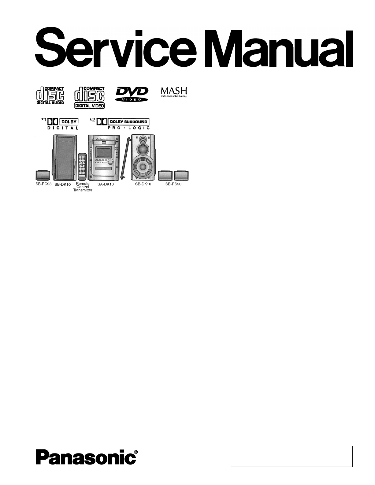
Panasonic SADK-10 Service manual
ORDER NO. MD010508 7C1
DVD Stereo System
SA-DK10
Colour
(S)... Silver Type
Area
(P)... U.S.A.
(PC)... Canada
TAPE SECTION :
AR2 MECHANISM SERIES
CD SECTION :
RAE0152Z-3 TRAVERSE DECK SERIES
A6
Specifications
■ AMPLIFIER SECTION
Stereo mode power output
THD 10% Total harmonic distortion
LF 75 Hz 65 W per channel (8 Ω)
HF 1 kHz 30 W per channel (6 Ω)
Total stereo mode power
LF 55Hz - 100 Hz 65 W per channel (8 Ω)
HF 100Hz - 15 kHz 28 W per channel (6 Ω)
Power output in Home Theater mode
THD 10%, both channels driven
Front
LF 75 Hz 65 W per channel (8 Ω)
HF 1 kHz 30 W per channel (6 Ω)
Center 1 kHz 40 W (8 Ω)
Surround 1 kHz 35 W per channel (8 Ω)
Total power output 300 W
Input sensitivity
AUX 250 mV
Input Impedance
AUX 10 kΩ
■ FM TUNER SECTION
Frequency range 87.9 - 107.9 MHz (200 kHz steps)
87.5 - 108.0 MHz (100 kHz steps)
Sensitivity 1.8 µV (IHF)
S/N 26 dB 1.5 µV
Antenna terminal(s) 75 Ω (unbalanced)
■ AM TUNER SECTION
Frequency range 520 - 1710 kHz (10 kHz steps)
Sensitivity
S/N 20 dB (at 1000 kHz) 500 µV/m
■ CASSETTE DECK SECTION
Track system 4 track, 2 channel
Heads
Record/playback Solid permalloy head
Erasure Double gap ferrite head
Motor DC servo motor
Recording system AC bias 100 kHz
Erasing system AC erase 100 kHz
Tape speed 4.8 cm/s (1 7/8 ips)
Frequency response (+3 dB, -6 dB at DECK OUT)
NORMAL (TYPE I) 35 Hz - 14 kHz
HIGH (TYPE II) 35 Hz - 14 kHz
S/N 50 dB (A weighted)
Wow and flutter 0.18 % (WRMS)
Fast forward and rewind time Approx. 120 seconds with
C-60 cassette tape
■ Disc SECTION
Disc
DVD-Video
© 2001 Matsushita Electronics (S) Pte. Ltd. All rights
reserved. Unauthorized copying and distribution is a
violation of law.
SA-DK10
8 cm/12 cm single sided, single layer
8 cm/12 cm single sided, double layer
8 cm/12 cm double sided, double layer
(One layer per side)
Video CD/CD 8 cm/12 cm
Video
Signal system NTSC
Output level
Composite video 1Vp-p(75Ω)
S-Video Y 1Vp-p(75Ω)
S-Video C 0.286 Vp-p (75 Ω/NTSC)
Audio
Sampling frequency
CD 44.1 kHz
DVD 48kHz/96 kHz
Decoding 16/20/24 bit linear
Wow and flutter Below measurable limit
D/A converter Delta-sigma DAC)
Pick up
Beam source Semiconductor Laser
Wavelength
DVD 658 nm
VCD/CD 790 nm
■ GENERAL
Power supply AC 120 V, 60Hz
Power consumption 161 W
Power consumption in standby mode
161 W
Dimensions (W x H x D) 215.4 X 315 X 350 mm
8 1/2” x 12 13/32” x 13 25/32”
Mass (7.8 kg) 17.2 lb
■ SYSTEM
SC-DK10(P) Music Center: SA-DK10(P)
Front Speaker: SB-DK10(P)
Surround Speaker: SB-PS90(P)
Center Speaker: SB-PC93(P)
SC-DK10(PC) Music Center: SA-DK10(PC)
Front Speaker: SB-DK10(P)
Surround Speaker: SB-PS90(P)
Center Speaker: SB-PC93(P)
Notes:
1. Specifications are subject to change without notice. Mass and
dimensions are aproximate.
2. Total harmonic distortion is measured by the digital spectrum
analyzer.
CONTENTS
Page Page
1 Safety Precaution
2 Before Repair and Adjustment
3 Protection Circuitry
4 Accessories
5 Handling Precautions For Traverse Deck
6 Precaution of Laser Diode
7 Operation Procedures
8 Disassembly and Main Component Replacement Procedures
3
9 Measurements and Adjustments
3
10 Illustration of ICs, Transistors and Diodes
11 Terminal Function of IC’s
3
4
12 Block Diagram
5
13 Schematic Diagram
14 Printed Circuit Board
6
7
15 Wiring Connection Diagram
16 Parts Location and Replacement Parts List
9
22
24
25
26
35
68
81
83
2
1 Safety Precaution
(This “Safety Precaution” is applied only in U.S.A.)
1. Before servicing, unplug the power cord to prevent an electric shock.
2. When replacing parts, use only manufacturer’s recommended components for safety.
3. Check the condition of the power cord. Replace if wear or damage is evident.
4. After servicing, be sure to restore the lead dress, insulation barriers, insulation papers, shields, etc.
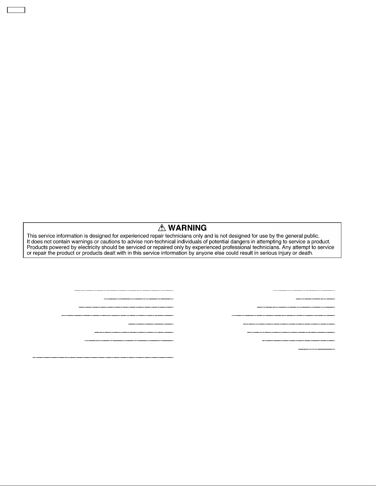
5. Before returning the serviced equipment to the customer, be sure to make the following insulation resistance test to
prevent the customer from being exposed to a shock hazard.
1.1. Insulation Resistance Test
1. Unplug the power cord and short the two prongs of the plug with a jumper wire.
2. Turn on the power switch.
3. Measure the resistance value with ohmmeter between the jumper AC plug and each exposed metal cabinet part, such as
screwheads, antenna, control shafts, handle brackets, etc.
Equipment with antenna terminals should read between 3 MΩ and 5.2 MΩ to all exposed parts*.(Fig.1)
Equipment without antenna terminals should read approximately infinity to all exposed parts.(Fig.2)
*Note: Some exposed parts may be isolated from the chassis by design. These will read infinity.
4. If the measurement is outside the specified limits, there is a possibility of a shock hazard. The equipment should be repaired
and rechecked before it is returned to the customer.
SA-DK10
2 Before Repair and Adjustment
Disconnect AC power, discharge Power Supply Capacitors C566~C569, C782 and C591 through a 10Ω, 5W resistor to ground.
DO NOT SHORT-CIRCUIT DIRECTLY (with a screwdriver blade, for instance), as this may destroy solid state devices.
After repairs are completed, restore power gradually using a variac, to avoid overcurrent.
Current consumption at AC 120V, 60 Hz in NO SIGNAL mode should be ~650mA.
3 Protection Circuitry
The protection circuitry may have operated if either of the following conditions are noticed:
• No sound is heard when the power is turned on.
• Sound stops during a performance.
The function of this circuitry is to prevent circuitry damage if, for example, the positive and negative speaker connection wires are
“shorted”, or if speaker systems with an impedance less than the indicated rated impedance of the amplifier are used.
If this occurs, follow the procedure outlines below:
1. Turn off the power.
2. Determine the cause of the problem and correct it.
3. Turn on the power once again after one minute.
Note :
When the protection circuitry functions, the unit will not operate unless the power is first turned off and then on again.
3
SA-DK10
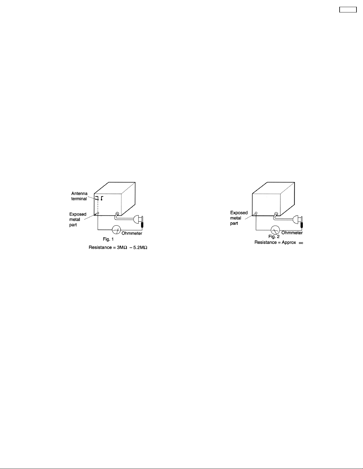
4 Accessories
Remote Control
Transmitter
FM indoor antenna
AC mains lead
AM Loop antenna
Video cable
4
5 Handling Precautions For Traverse Deck
SA-DK10
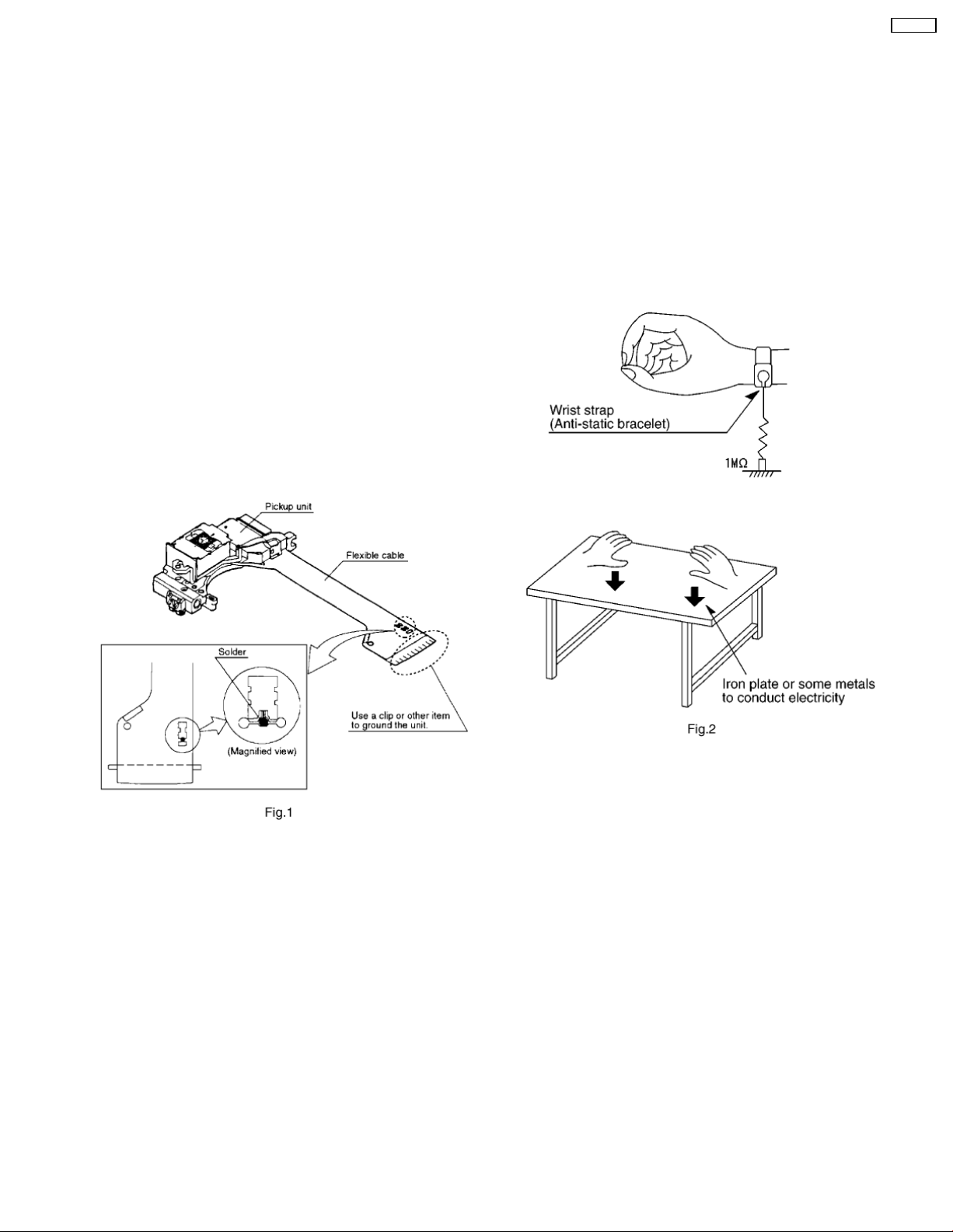
The laser diode in the traverse deck (optical pickup) may break
down due to potential difference caused by static electricity of
clothes or human body.
So, be careful of electrostatic breakdown during repair of the
traverse deck (optical pickup).
5.1. Handling the Traverse Deck
(Optical pickup)
1. The traverse deck (optical pickup) is an extremely
highprecsion construction and must not be subjected to
impact, excessive vibration, or other types of rough
handling.
2. In order to prevent static electricity damage to the laser
diode, use a short pin or similar tool to short the optical
pickup’s flexible circuit boards after they have been
disconnected from the main circuit board.
3. Handle the flexible circuit boards with care; excessive force
could cause them to be broken.
4. Do not turn the pre-set variable resistor (for adjustment of
the laser power); it has been adjusted at the factory. (as
shown in Fig. 1)
5.2. Grounding for electrostatic
breakdown prevention
1. Human body grounding
Use the anti-static wrist strap to discharge the static
electricity from your body.
2. Work table grounding
Put a conductive material (sheet) or steel sheet on the area
where the optical pickup is placed, and ground the sheet.
(sa shown in Fig. 2)
3.
Caution :
The static electricity of your clothes will not be grounded
through the wrist strap. So, take care not to let your clothes
touch the traverse deck (optical pickup).
5.3. Caution when Replacing the
Traverse Deck
The traverse deck has a short point shorted with solder protect
the laer diode against electrostatics breakdown. Be sure to
remove the solder from the short point before making
connections.
5

SA-DK10
6 Precaution of Laser Diode
CAUTION:
This product utilizes a laser diode with th unit turned “ON”,
invisible laser radiation is emitted from the pick up lens.
CAUTION!
THIS PRODUCT UTILIZES A LASER.
USE OF CONTROLS OR ADJUSTMENTS OR PERFORMANCE OF PROCEDURES OTHER THAN THOSE SPECIFIED HEREIN MAY RESULT
IN HAZARDOUS RADIATION EXPOSURE.
1. Do not disassembly the pick up unit, since radioation from
exposed laser diode is dangerous.
2. Do not adjust the variable resistor on the pickup unit. It was
already adjusted.
3. Do not lock at the focus lens using optical instrument.
4. Recommend not to lock up lens for long time.
6

7 Operation Procedures
SA-DK10
7
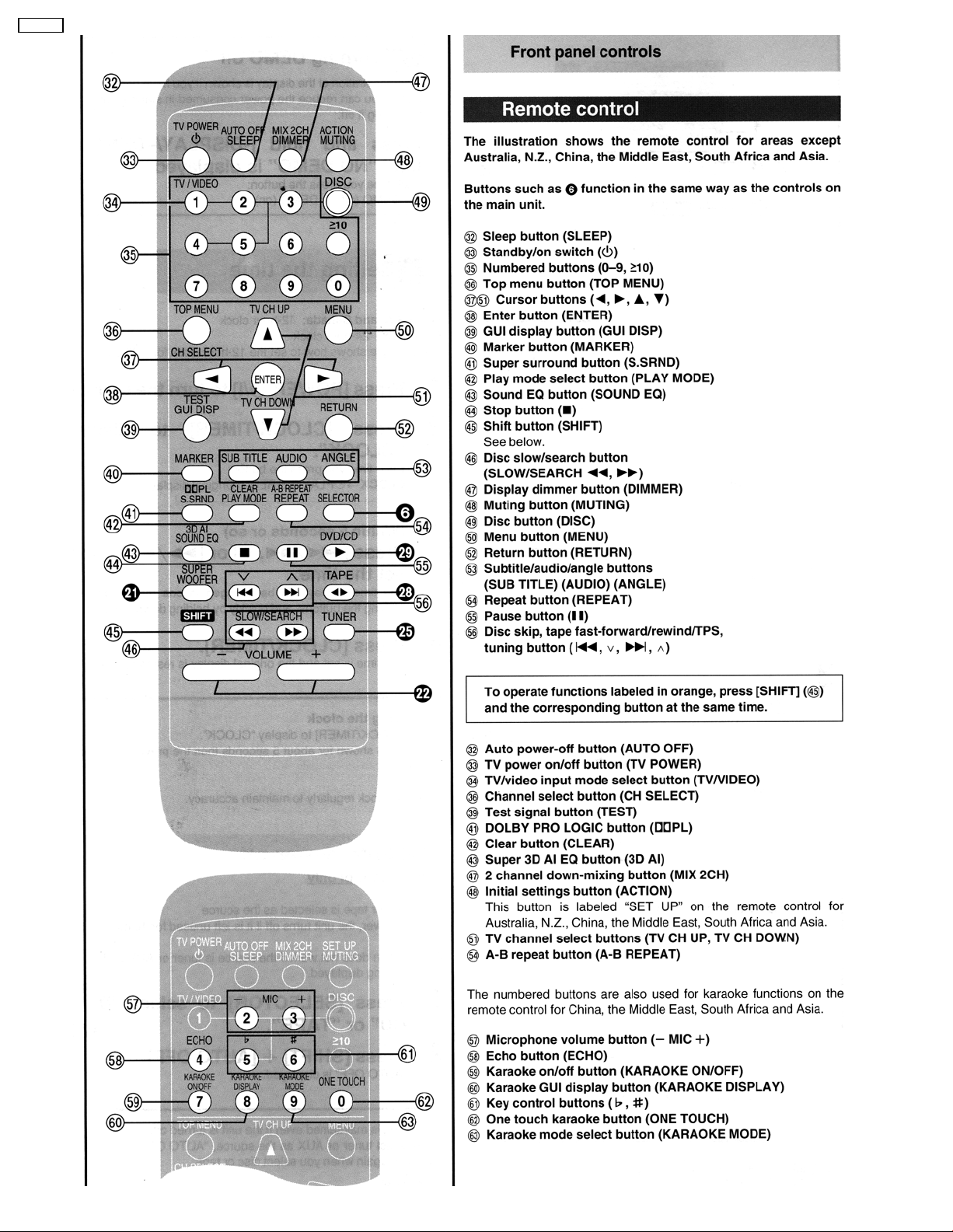
SA-DK10
8
8 Disassembly and Main Component Replacement
Procedures
SA-DK10
“ATTENTION SERVICER”
Some chassis components may have sharp edges.
Be careful when disassembling and servicing.
1. This section describes procedures for checking the operation of the major printed circuit boards and replacing the
main components.
2. For reassembly after operation checks or replacement, reverse the respective procedures.
Special reassembly procedures are described only when required.
3. Select items from the following index when checks or replacement are required.
Contents
• Checking Procedure For Each Major P.C.B.
1. Checking of the Main, Panel, Deck and Power P.C.B.
2. Checking for the DVD F/E Module P.C.B.
3. Disassembly for the DVD Changer Unit.
• Main Component Replacement Procedures
1. Replacement of the Traverse Deck.
2. Replacement of the Power Amplifier IC.
• Disassembly and assembly of the Traverse Unit
• Disassembly and assembly of the Disc Tray
Warning:
This product uses a laser diode. Refer to caution statement Precaution of Laser Diode.
9
SA-DK10
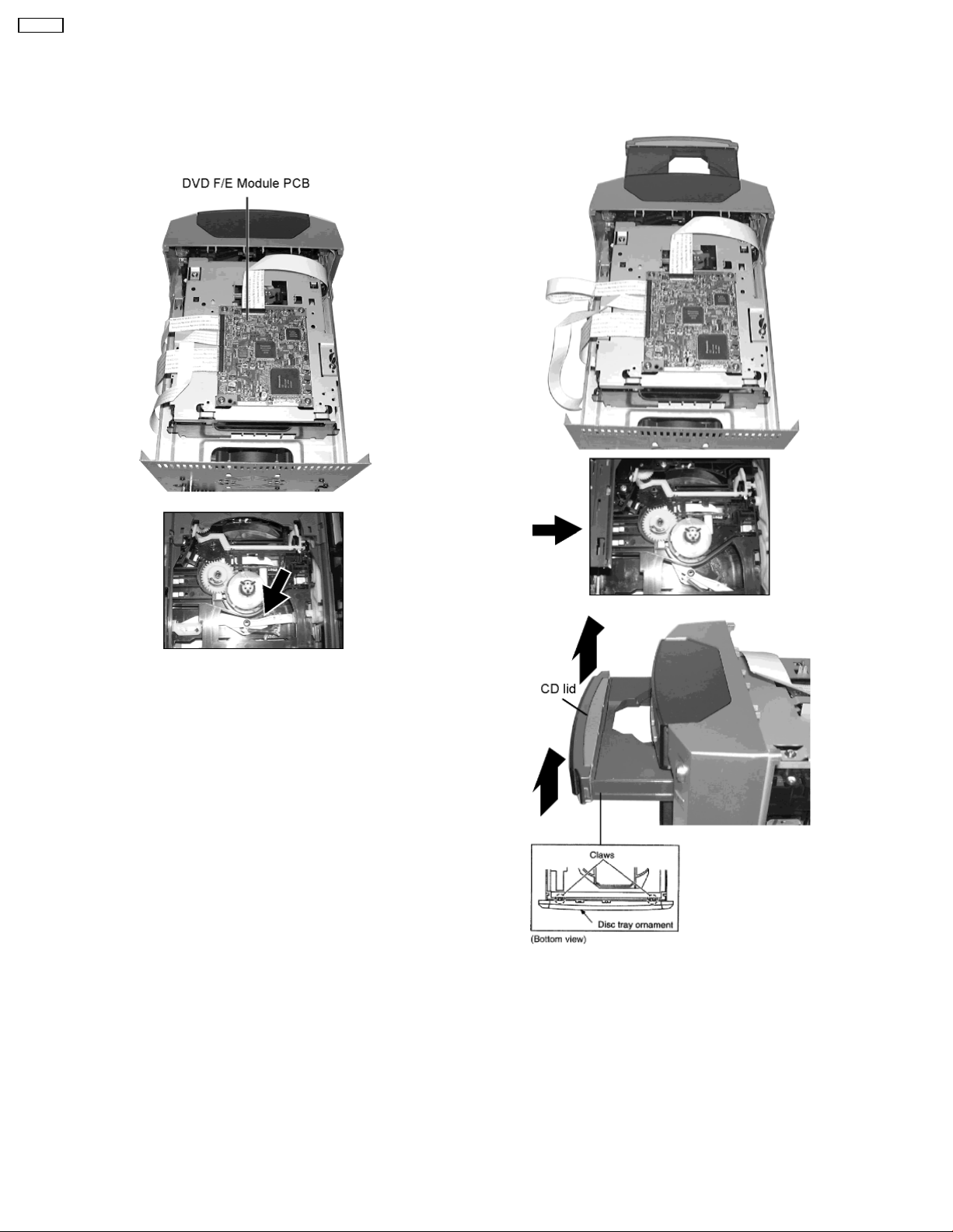
8.1. Disassembly Procedure for each major P.C.B. Checking
8.1.1. Checking of the DVD Servo, Main, Transformer, Panel and Deck P.C.B.
Step 1 Remove the top cabinet.
Step 2 Push lever in the direction of arrow.
Step 3 Pull out the CD tray as shown. Release the 2 claws and
remove the CD lid. Push back the CD tray after the CD lid has
been removed.
10
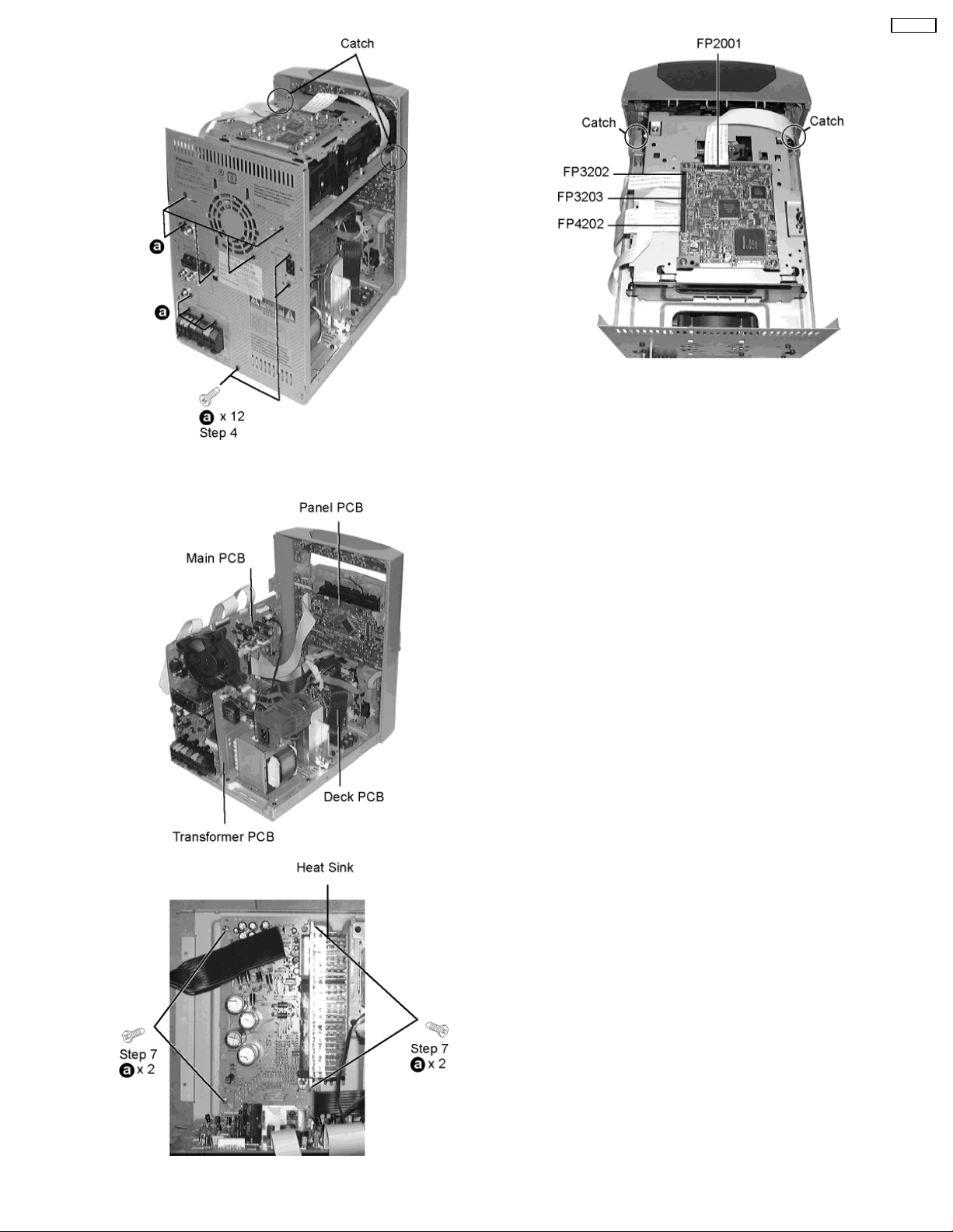
Step 4 Remove 12 screws and catches both side.
• Checking for Panel P.C.B., Main P.C.B. and Deck P.C.B..
SA-DK10
Step 5 Remove the wires at FP2001, FP3202, FP3203, and
FP4202.
Step 6 Release the wire from catch, remove the CD changer
base together with the CD changer.
11
SA-DK10
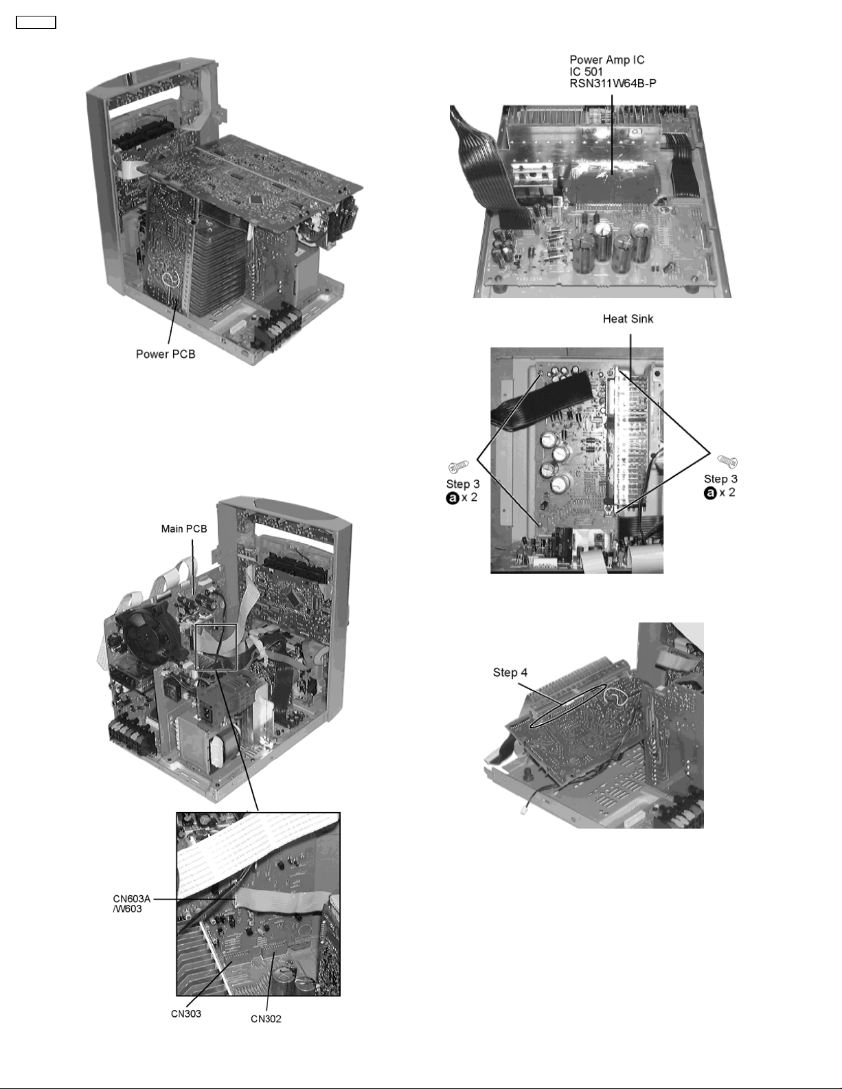
• Checking for Power P.C.B.
• Replacement of the Power Amplifier IC and Regulator
Transistor.
Step 1 Follow the procedures in “Checking procedure for each
major P.C.B.
Step 2 Remove the wires at CN302, CN303 and H603A/W603
and pull out the Main P.C.B..
Step 3 Remove 4 screws fixed to the Power Amplifier IC and
Transistor Holders.
Step 4 Unsolder the terminals of Power Amp IC and replace
the component.
12
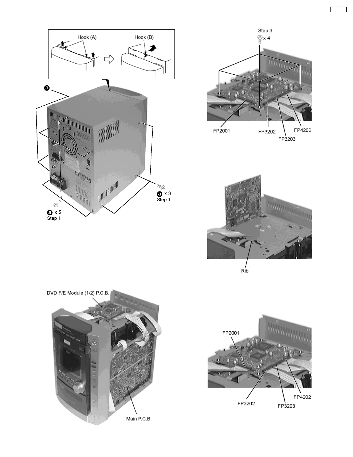
8.2. Checking for the Main and DVD F/E Module (1/2) P.C.B.
Step 3 Remove 4 screws.
Step 4 Remove 4 connectors.
Step 5 Pull out 4 FFCs.
SA-DK10
Step 1 Remove 3 screws each both side and 5 screws at rear
panel.
Step 2 Lift up the both sides cabinet ass’y to release the hook
(A). Then pull the cabinet ass’y toward the rear and release the
hook (B) to remove the cabinet ass’y.
NOTE: When installing the cabinet ass’y, take care not to
damage the front cabinet ass’y from hook (B).
• Check the Main P.C.B. and DVD F/E Module (1/2) P.C.B..
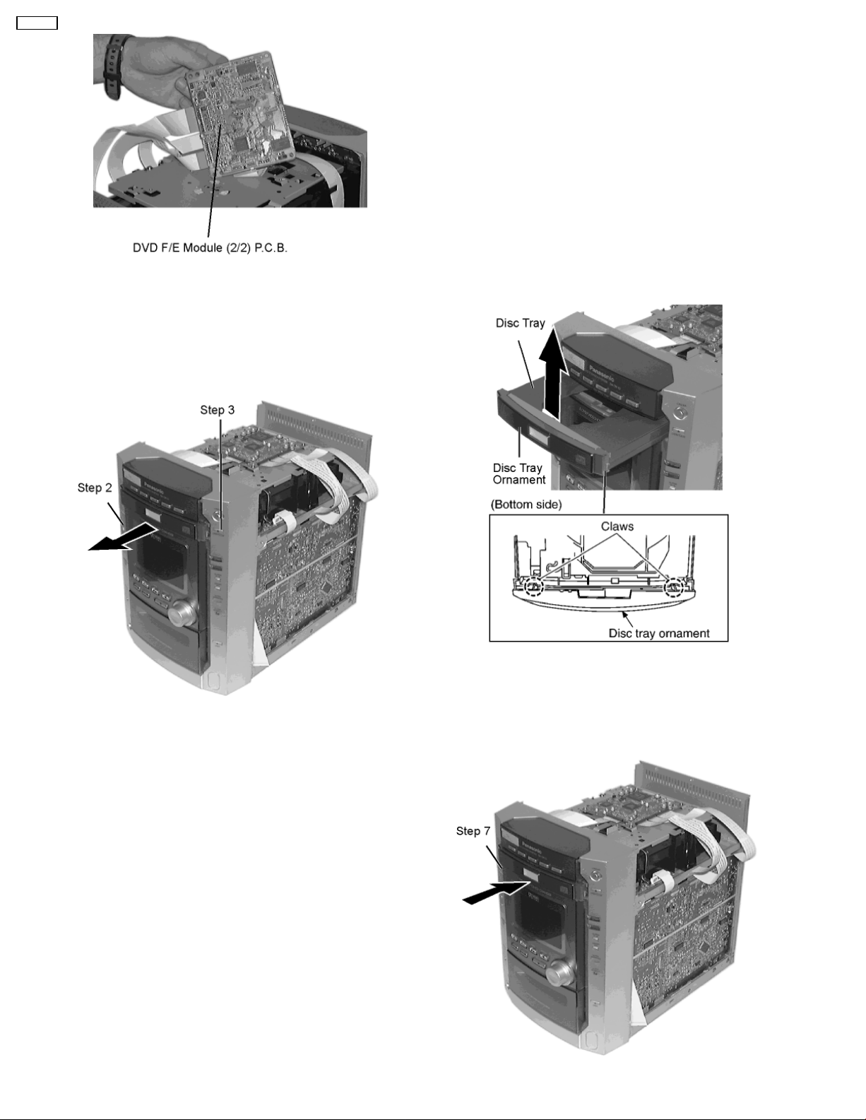
Step 6 Raise the DVD Module P.C.B..
• Checking the DVD F/E Module (2/2) P.C.B. as shown
below.
Step 7 Disconnect the FFCs to the connector.
Step 8 Lift up DVD F/E Module (2/2) P.C.B. as shown.
13
SA-DK10
8.3. Disassembly for DVD/CD changer unit
8.3.1. Disassembly for the disc tray
ornament
• Follow the (Step 1) - (Step 3) of item 8.1
When opening the disc tray automatically
Step 1
Step 2
Step 3
open automatically. (If the other buttons would be push, disc
tray would be open.)
Connect the power.
Push the button and the power turns ON.
Push the open/close button, so the disc tray will be
Step 4
Step 5
ornament.
Step 6
Step 7
Disconnect the power.
Connect the power again.
Push the button and the power turns ON.
Release the 2 claws, and then remove the disc tray
14
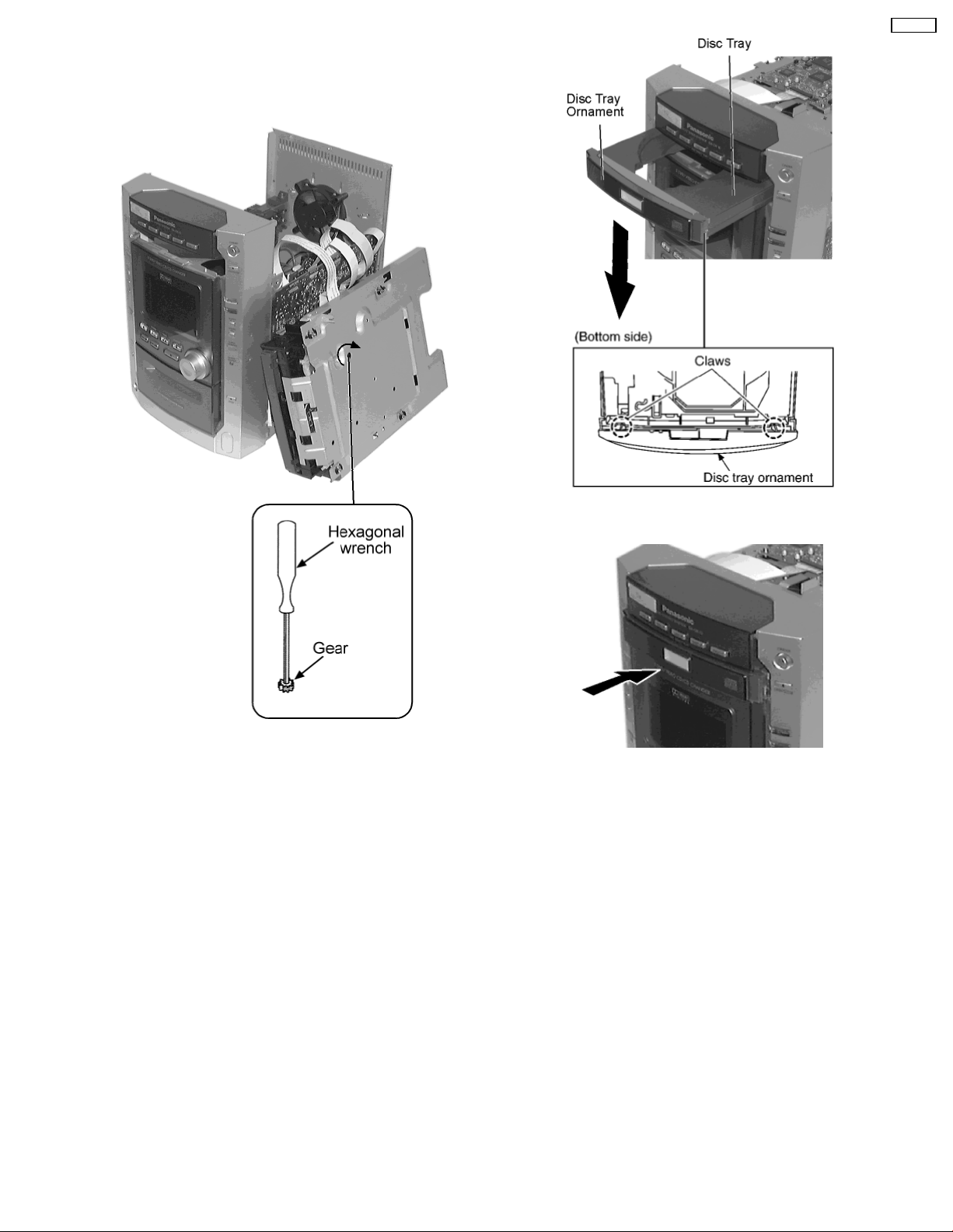
Step 8 Push the open/close button1, so the disc tray will be
close.
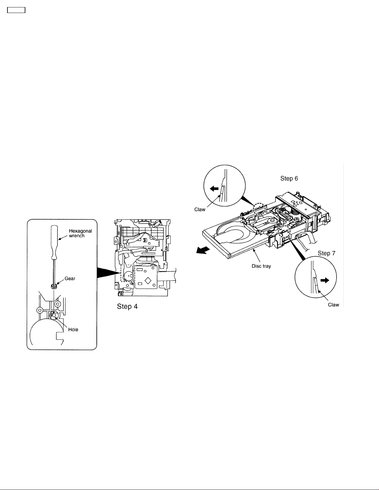
When opening the disc tray manually
Step 1 Off the unit.
SA-DK10
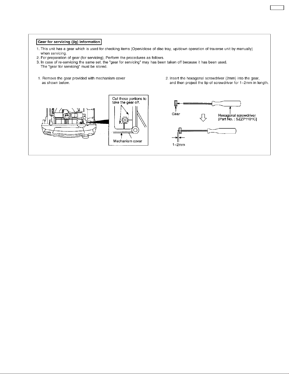
Step 2 Insert the gear for servicing into the bottom hole of
mechanism unit cover, and then rotate the hexagonal wrench
clockwise so the disc tray will be open.
Step 3 Release 2 claws, and then remove the disc tray
ornament.
Step 4 Push the disc tray.
15
SA-DK10
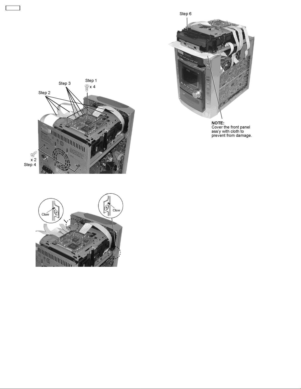
8.3.2. Disassembly for the DVD/CD
changer unit.
• Follow the (Step 1) - (Step 3) of item 8.1
• Follow the disassembly instruction for the disc tray
ornament .
Step 1
Step 2
Step 3
Step 4
Remove 4 screws.
Pull out 4 FFCs.
Remove 4 connectors.
Remove 2 screws at rear panel.
The preparation of checking procedures in operational
condition is completed.
Step 5
DVD changer unit.
Step 6
changer unit on the unit.
Release the claws of both ends, and then lift up the
Remove the DVD/CD changer and place the DVD/CD
16
8.4. Main Component Replacement Procedures
SA-DK10
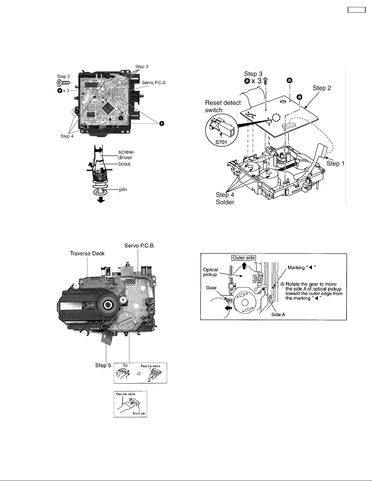
1. Replacement of the Traverse Deck
Step 1 Follow the procedures in ‘Disassembly of the Traverse
Unit’ ( Step 1 - Step 4 )
Insert a short pin into the flexible cable for traverse unit.
• Installation of the CD servo P.C.B. after replacement
Step 1 Connect the FFC board.
Step 2 Install the CD servo P.C.B. in the traverse deck
assembly.
Step 3 Desolder the 4 legs of the 2 motors and pull out the
Servo P.C.B.
Step 4 Widen the 3 bosses with a flat screwdriver and pull out
the 3 pins. Then remove the Traverse Deck.
Note:
Before installing the CD servo P.C.B., move the optical pickup
towards the outer edge from the marking (black triangle).
[Otherwise, the reset detect switch (S701) mounted on the CD
servo P.C.B. may be damaged.]
2. Replacement of the Power Amplifier IC
Step 1 Follow the procedures in ‘Checking Procedure for each
major P.C.B.’ ( Step 1 - Step 4 ).
Step 5 Remove the flexible cable CN 701.
• Removal of the flexible cable. Push the top of the connector
in the direction of the arrow 1, and then pull out the flexible
cable in the direction of the arrow 2.
Note:
17
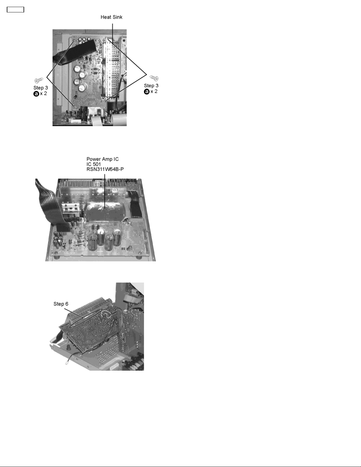
SA-DK10
Step 2 Remove the wires at CN302, CN303 and CN304 and
pull out the Main P.C.B.
Step 3 Remove 4 screws fixed to the Power Amplifier IC.
Step 4 Unsolder the terminals of Power Amp IC and replace
the respective component.
18
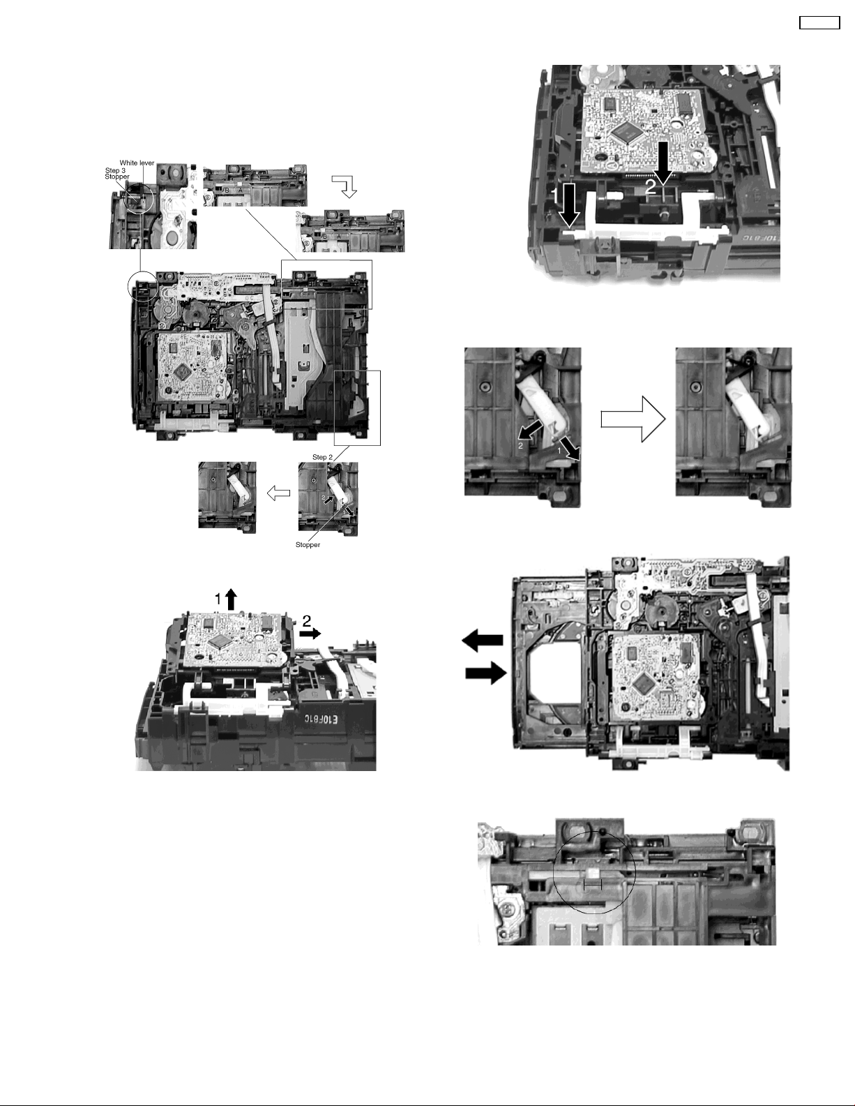
8.5. Disassembly and assembly of the Traverse Unit
Step 1 Push the lever from position A to B.
Step 2 Pull the stopper (black) in the direction of arrow 1 and
push the lever in the direction of arrow 2.
Step 3 Push the stpeer (black) down until the white lever eject
out.
Step 3 Pull the stopper in the direction of arrow 1 and release
the lever in the direction of arrow 2 as shown.
SA-DK10
Step 4 Lift up the traverse unit and slide out the unit as shown.
• Replacement of Traverse Unit
Step 1 Place the traverse unit as shown.
Step 2 Press in the lever shaft in the direction of arrow 1 as
shown and push the traverse unit into the position in the
direction of arrow 2.
Step 4 Pull out the tray half way and push it back fully.
Step 5 Push the lever to the initial position indicated ‘I---I’.
19
SA-DK10
8.6. Disassembly and assembly of the Disc Tray
Step 5 Rotate the hexagonal wrench in the direction of arrow
(clockwise), and then open the disc tray fully.
Step 2 With lifting the claw in the direction of arrow 1, draw the
clamp SW P.C.B. in the direction of arrow 2.
Step 3 Remove the mechanism cover.
Step 4 Insert the gear with hexagonal wrench into the hole.
Step 6 Upset the CD changer unit again.
Step 7 Release both the claws, and then draw the disc tray.
20
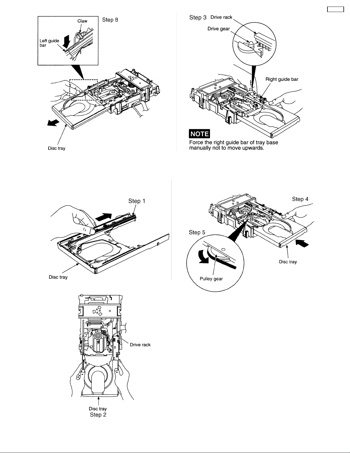
SA-DK10
Step 8 With forcing the left guide bar manually because the left
guide bar interfers with claw, draw the disc tray.
• Installation of the disc tray after replacement
Step 1 Slide the drive rack fully in the direction of arrow.
Step 3 Align the drive rack with the driver gear.
Step 4 Holding the disc tray manually, rotate the pulley gear in
the direction of arrow.
Step 5 Rotate the gear 5 or 6 times manually, and then push
the disc tray.
Step 2 Holding the drive rack not to move, install the disc tray.
21
SA-DK10
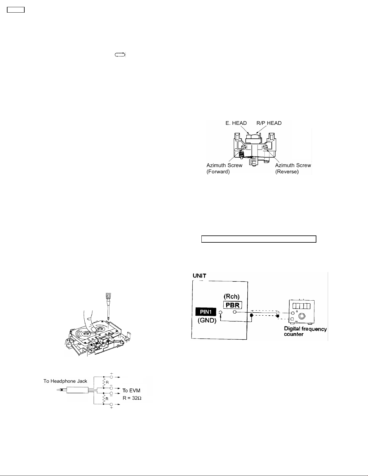
9 Measurements and Adjustments
9.1. Cassette Deck Section
• Measurement Condition
− Reverse-mode selector switch:
− Tape edit: NORMAL
− Record timer: OFF
− Make sure head, capstan and press roller are clean.
− Judgeable room temperature 20 ± 5 °C (68 ± 9°F)
• Measuring instrument
9.1.1. Head Azimuth Adjustment
Note :
If you wish to readjust the head azimuth, be sure to adjust with
adhering the casette tape closely to the mechanism by pushing
the cebter of cassette tape with your finger. (Shown in Fig. 1)
1. Connect the measuring instrument as shown in Fig. 2.
2. Replace azimuth screws for both forward and reverse
direction after removing the screw-locking bond left on the
head base.
3. Playback the azimuth adjustment portion(8kHz, -20dB) of
test tape(QZZCFM). Adjust the azimuth adjusting screw
until the outputs of the L/Rch are maximized. (Refer to Fig.
3)
Make sure that the difference in the peak level between the
left and right channels does not exceed 5dB.
4. Perform the same adjustment in reverse playback mode.
Check of the level difference forward and reverse
directions
5. Playback the playback gain adjustment portion(315Hz,
0dB) of test tape(QZZCFM). Check if level difference
between forward and reverse direction is within 1.5dB.
6. After the adjustment, apply screwlock to the azimuth
adjusting screw.
− EVM (Electronic Volmeter)
− Digital quency counter
• Test Tape
− Head azimuth adjustment (8 kHz, -20 dB); QZZCFM
− Tape speed gain adjustment (3 kHz, -10 dB);
QZZCWAT
− Playback gain adjustment (315 Hz, 0 dB); QZZCFM
− CrO2 tape, QZZCRX
Fig. 3
9.1.2. Tape Speed Adjustment (Deck 1/2)
1. Set the tape edit button to “NORMAL” position.
2. Insert the test tape (QZZCWAT) to DECK and playback
(FWD side) the middle portion of it.
3. Adjust Motor VR for the output value shown below.
Adjustment target: 2940~3060 Hz (NORMALspeed)
4. After alignment, assure that the output frequency of the
DECK REV is within ±60 Hz respectively of the value of the
output frequency of DECK FWD.
Fig. 1
Fig. 2
9.1.3. Bias and Erase Voltage Check
1. Set the unit “AUX” position.
2. Insert the Normal blank tape (QZZCRA) into DECK and the
unit to “REC” mode (use “● REC/PAUSE” key).
3. Measure and make sure that the output is within the
standard value.
4. Insert the Cr02 tape(QZZCRX).
5. Repeat steps 2 and 3.
Bias voltage 16 ± 4mV (Normal)
26 ± 5mV (Cr02)
Erase voltage for Deck 2 more than 80mV (Normal)
more than 90mV (Cr02)
22
9.1.4. Bias Frequency check
1. Set the unit to “AUX” position.
9.2. Alignment Points
Cassette Deck Section
SA-DK10
2. Insert the Normal blank tape (QZZCRA) into DECK 2 and
set the unit to “REC” mode (● use “REC/PAUSE” key).
3. Check so that the output frequency is within the standard
value.
Standard Value: 86 ±8 kHz
23

SA-DK10
10 Illustration of ICs, Transistors and Diodes
BU2090AF-E2 (16P)
M62457AFPE1 (16P)
M62456FPE1 (24P)
NJU7313AMT2 (30P)
M5218AFPE3 (8P)
BU4053BCF-E2 (14P)
M5228FPE1 (14P)
PQ1CZ31H2ZP
PQ018EZ01ZP
M62444FPE1
KM416S1DTG8T (60P)
C2BBFD000307 (42P)
C2BBFD000308 (42P)
C0CBCBD00002 (6P)
C1AB00001393 (16P)
C1DB00000582 (16P)
M5218AP
5
8
4
1
C0CBCBE00001 C3EBEC000024
2SC3940AQSTA
E
E
C
C
B
B
IMX9T110
B
B
C
E
C
Cathode
2SB1115-T1
B
2SB621ARSTA
2SD965RTA
KTA12710YTA
E
E
C
E
C
B
UDZSTE175R1B
UDZSTE177R5B
Ca
Anode
A
1SS355TE17
1SS380TE-17
Cathode
Anode
A
UDZSTE179R1B
DAP202KT146
DA204KT146
Cathode
Ca
Anode
Cathode
No.1
BA7755A
1
5
2SB1417PQTA
B
C
E
A
Anode
1D3E
RL1N4003N02
1N5402BM21
Cathode
A
Anode
SLR325MCT31W
Anode
Cathode
A
Ca
MN677533MP (208P)
MN103S13BGA (144P)
MN67706EC (100P)
AN8708FHK
MN102H60GFA (100P)
C0JBAA000001
PST596JNR
RFKFRV45C040
2SD2144STA
KRA102MTA
KRC102MTA
KTC3199GRTA
RVTDTC143EST
2SC2784FTA
Cathode
MTZJ30BTA
MTZJ4R7BTA
MTZJ6R8ATA
Ca
MTZJ16ATA
MTZJ9R1CTA
MA728TX
Ca
Anode
A
SELS5923C
Anode
A
Ca
Cathode
Cathode
C2BBGF000280 (100P)
C2HBZC000011 (80P)
C0FBBK000021 (48P)
KTC2026
KTA1046YU
KTA1046YTA
RSN311W64A-P
1
..................
2SA1037AKSTX
2SC2412KT96R
2SD2144K1
DTA114EKA146
DTA143XKA146
DTC114YKA146
MA165TA
MA700ATA
MA729TX
RVD1SS133TA
KRC103STA
MA111TX
Cathode
Ca
Anode
A
LNJ201LPQJA
Anode
A
Cathode
Ca
LM2940T5M
I
G
No.1
TA7291P
1
10
0N2180RLC1
4
1
3
2
4
1
26
2
3
O
AN7326K
C0GBG0000020
28
22
1
7
21
8
14
STK470-050A
1
14
15
DTC143XKA146
DTC114EKA146
C
DTC144TKA146
UN5212TX
UN2121-TX
KRC103STA
B
E
RK306LFU1
Ca
A
Anode
SFPB-72V
Anode
A
Ca
Cathode
Cathode
Ca
A
Anode
MA8047MTX
Anode
Ca
Cathode
Cathode
Ca
A
24
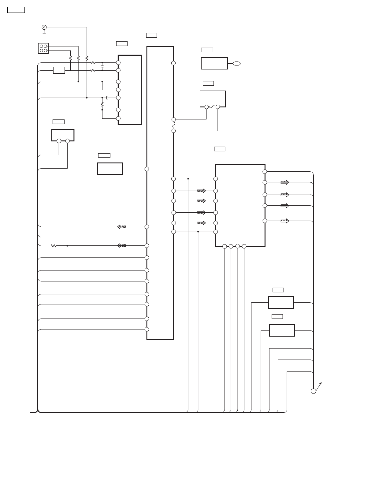
11 Terminal Function of IC’s
SA-DK10
11.1. IC601 (C2BBGF000280 )
System Microprocessor
Pin No.
1 SER5 I/O Searal 5 output (PLL/DSP DA)
2 MK_IN2 I/O Mech condition input 2
3 MK_IN1 I/O Mech condition input 1
4 KEY 3 I/O Key 3 input
5 KEY 2 I/O Key 2 input
6 KEY 1 I/O Key 1 input
7 JOG1B I/O JOG 1 input B Main Volume
8 JOG1A I/O JOG 1 input A Main Volume
9 SP_IN I/O Speana input
10 SP_A I/O Speana control output A
11 AP_B I/O Speana control output B
12 SP_C I/O Speana control output C
13 N.C. I/O No use
14 N.C. I/O No use
15 N.C. I/O No use
16 SER9 I/O Searal 9 output (Echo LA)
17 VSS - Ground
18 RESET I RESET input (Active L)
19 XCOUT I/O 32.768 kHz sub clock
20 XCIN I/O 32.768 kHz sub clock
21 VSS - Ground (0V)
22 XIN I 4.00 MHz main clock
23 XOUT O 4.00 MHz main clock
24 VCC - Power supply (+5V)
25 MBP1 I/O MPU beat proof output 1
26 MBP2 I/O MPU beat proof output 2
27 PCONT/PCNTI/O PCNT output
Mark I/O Function
(TPS/PHOTO)
(HALF/MODE/R_INHF/R_INHR)
Pin No.
98 VREF - Reference for A-D
99 SER7 I/O Searal 7 output (PLL CE)
100 SER6 I/O Searal 6 output (PLL/DSP CK)
Mark I/O Function
28 N.C. I/O No use
29 DCDET I/O DCDET input
30 SER4 I/O Searal 4 output (ROM CS)
31 RMT I/O Remoco input
32 SYNC I/O AC failure detect input
33 SER3 I/O Searal 3 output (Exp2 CK/ROM
34 SER2 I/O Searal 2 output (Exp1CK/ROM
35 SER1 I/O Searal 1 output (EXP1/2 DA)
36 DSPRST I/) DSP reset output
37 DSPACK I/O DSP ACK input
38 SENSE I/O DSP sense input
39 MIC SW I/O MIC output sw
40 PHONE I/O Phone output sw
41 D0/ST I/O Tuner D0/ST input
42 SDIN I/O Tuner signal DET input
43 REGION
IN/REG_IN
44-55 AND12-
1/REG12-1
56-88 SEG1-33 I/O Segment drive output (Anode
89 VEE - Power supply (-30V)
90 MECHSI I/O Mecha control data input
91 MECHSO I/O Mecha control data output
92 MECHCK I/O Mecha control clock input
93 MECHRQ I/O Mecha con request output
94 MECHCS I/O Mecha control CS input
95 MECRST I/O Mechcon reset output
96 SER8 I/O Searal 8 output (DSP LA)
97 AVSS - Analog ground (0V)
CK)
DA)
I/O Region input
I/O Grid drive output (Digit drive
output)
drive output)
25
SA-DK10
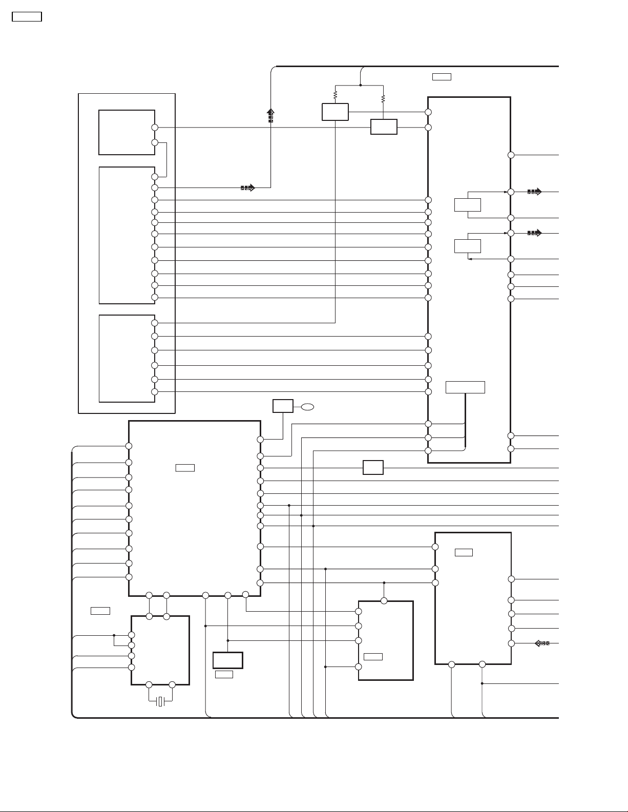
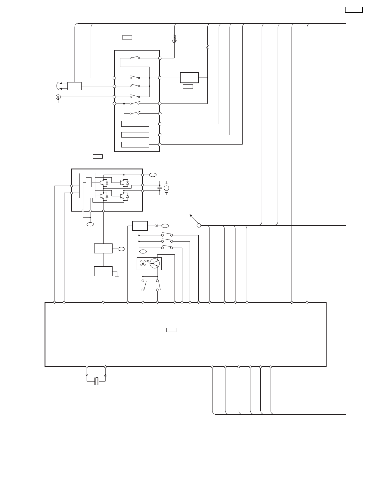
12 Block Diagram
OPTICAL PICKUP UNIT
HIGH FREQUENCY
DVD MODULATOR
CD MODULATOR
AMUTE
SDATA
SCLOCK
CMD
STATUS
DSPCLK
YDET
YVDL
STBDAC2
B
IC6501
C1DB00000582
CLOCK
CLK27M
EXTCLK
CLK16M
MODULATOR
64
AN2
56
SBO 4
53
SBT4
51
SBI3
52
SBO3
50
P82
63
AN1
49
DAC1
68
LCAS
7,18,78
3
4
10
13
LD-OUT
CLK27
CLK64
76BIS
CLK16
LD-IN
LD
SW
T2
T1
Mon
F2
F1
RFN
RFP
T4
T3
LD
F2
F
E
F1
Mon
AN323OSCI
65
14 15
FSEL
XTO
2
5
15
14
5
4
8
13
12
11
10
7
6
11
10
8
6
4
2
IC6201
MN102H60GFA
CPU
CLK33
XTI
78
93~100
NRST
82
8,41,42
RESET
IC6301
PST596JNR
VREF+
AN6,AN5
SBI1
SBT1
SBO1
TILTP
Q5215
QR5251
SWITCH
+B
80
47
AN7
79
PA4
46,45
76
PA0
71
70
72
1,6,13
2,3,
14~16,
26~33,
84~91
35~40,77
CD
SUPPLY
SWITCH
30,32,34,36,
39,41,43,45
16,17,26
6~8,11,
18~25,28,
29,31,33,
35,38,40,
42,44
LPCO1
Q5211
QR6301
RESET
SWITCH
1~5,
37,38,
40~48
12
XRESET
IC6302
RFKFRV45C040
4M FLASH ROM
LD
SUPPLY
SWITCH B
IC5201
AN8707FHK
FRONT END PROCESSOR
5
LPDO2
3
LPDO1
44
VIN2
43
VIN1
2
LPC1
41
VIN8
40
VIN7
33
RFINN
32
RFINP
46
VIN4
45
VIN3
38
VIN5
47
VIN9
48
VIN10
39
VIN8
4
LPC2
9
SEN
10
SCK
11
STDIO
32,57,58
30,31,45~55,
59,60,62,63,
68~70,72~74
26,37,
38,40~43
1,3,6,9,12,
14,17,20,24,
131,137,143
TRACKING
BALANCE
FOCUS
BALANCE
INTERFACE
IC7001
MN103S13BGA
CPU
85
NRST
FLTCP,
FLTON
TBAL
FBAL
RFENV
TESTSG
BDO
OFTR
BLKCK
ODCI1
26,27
TE
13
7
FE
20
6
36
21
FS
31
16
15
80
BD0
81,82,88,
90~92,
95~98,
109~111
97
100
112~115
X6501
SBI1
SBT1
SBO1
B1
C
NRST
D
26
TILTP
SA-DK10
LPCO1
97
AD6
54
TILTP
8,9
ARF,NARF
2
AD1
34
TRCRS
43
TBAL
3
AD0
IC2001
MN67706EC
44
100
50
DSC
FBAL
A03
1
A02
TSTSG
IC2501
C0GBG0000020
MOTOR DRIVE
VO3-
VO3+
VO4-
VO4+
VO2+
VO2-
VO1+
VO1-
STEPPING MOTOR UNIT
18
17
16
15
STEPPING MOTOR
-
M2501
M
+
-
M2502
M
+
OPTICAL PICK UP UNIT
ACTUATOR
FOCUS
12
11
14
13
ACT F+
ACT F-
ACT T+
ACT T-
COIL
TRACKING
COIL
CLK16M
85,86
61~63,
65~71,
76,83
77~80
49
47
84
87
90
88
89
83
48
BDO
OFTR
XRESET
ENS,ENC
CPUIRQ
CPUDTOUT
CPUCLK
CPUDTIN
TX
SYSCLK
DAT3~DAT0
TRSDRV
DA1,DA0
SPDRV
TILTIN
TILT
DTRD
IC6251
C0CBCBE00001
8
VIDEO
51
5,6
52
99
A04
56
55
SW2501
59
VCC
26
TRIN
3,2
VIN2,VIN1
23
VIN3
8
OPOUT
27
MUTE3
9
MUTE1
27
SA-DK10
K1
VIDEO OUT
JK701
VIDEO OUT
G
Y
C
CDET
WIDE1
CR/R
Y
SCLOCK
SDATA
CR/R
Y
YDET
YVDL
C
QR3301
AMP
IC6303
C3EBEC000024
EEPROM
6
5
15
12
11
10
2
+
5
6
IC3091
C0CBCD00002
REGULATOR
IC3301
C1AB00001393
VIDEO BUFFER
C-IN
C-OUT
CV-OUT
CV-SAG
Y-IN
Y-SAG
Y-OUT
118,123,
128,133
35~38,40~43,
45~47,49~51,
54~57,59,31
IC3001
MN677533MP
AV DECORDER
VCOUT
AOUT1,AOUT2
129
VCOUT
134
VYOUT
131
VREFY
LVDD
EXTCK
AOUT0
LRCK
SRCK
X HINT
174
1~10
110
92
93~94
89
90
158~208
IC3051
PQ018EZ01ZP
REGULATOR
IC3061
KM416S1DTG8T
SDRAM
IC4211
C0FBBK000021
6CH AUDIO
D/A CONVERTER
38
45
46,47
41
40
3712
SCLK1
DIN1
DIN2,DIN3
LRCIN
BCK IN
RSTB
33
MDO
+B
48
ZFLG1
12(11)
VOUT3
(VOUT4)
10
VOUT5
9
VOUT6
VOUT1
14(13)
(VOUT2)
ML
MC
MDI
36
35
34
ZFLAG
SL
CNT
SW
FL
CDET
D
B
B1
CLK27M
70~73,
75~78,
80~83
27,32,
33,
60~69
60~63,
65~67,
69
119
VBOUT
IC6222
C0JBAA000001
INVERTER
IC6221
99
CLK27
C0JBAA000001
INVERTER
STATUS
DSPCLK
AMUTE
CMD
WIDE1
TO MAIN
UNIT
D
EXTCLK
NRST
SBI1
SBO1
SBT1
STBDAC2
STATUS
DSPCLK
AMUTE
CMD
WIDE1
28
SER7
PBL(R)
IC201
NJU7313AMT2
SELECTOR
3(29)
MXL
LIN(R)
DATA
SA-DK10
ST
CK
AMUTE
ZFLAG
MUTE
PWCONT
FROM IC601
JK201
AUX1
TUNER
5
6
4(28)
5(24)
2(30)
9
Level shift
Latch circuit
Shift register
IC1
TA7291P
MOTOR DRIVE
Vs
REG
IN1
IN2
Vref
Vcc
GND
147
+B
Q451
SWITCH
OUT1
OUT2
Q1
POWER
SUPPLY
CONTROL
+B
+B
6(26)
7(24)
8
17
DATA
16
CK
14
ST
8
-B
2
10
M
+B
RM1
M5218AFPE3
SW2
SW1
SW3
OP
AMP
IC202
TO DVD UNIT
ZFLAG
D
CMD
DSPCLK
STATUS
AMUTE
WIDE1
33 32
CW
CCW
Q452
PLUNGER
SUPPLY
CONTROL
XOUT
20 19
X451
SW5
SW4
26
PLG
XIN
34 28
HALF
39
27 5
SW4
SW5
PSTN
IC451
C2BBFD000307
MECHA-CONTROL
31 30
SW3
SW1
29
SW2
35
DVD_CLK
DATA011DATA1
DATA0
36
DVD_CMD
12
DATA1
14
37
WIDE 1
DVD_STAT
B_CLK10B_CS9B_REQ8REST
B_CLK
B_CS
B_REQ
4
MUTE
PWCONT
18
REST
29
SA-DK10
PBL(R)
P.B. HEAD
FILTER
R/P HEAD
4
2
IC1000
BA7755A
ANALOG SWITCH
22(1)
+
+
21(2) 20(3) 19(4) 18 17 16 15 14 13 12 10
ALC
REC
PB LIN(R)
3
Q1317
BEAT PROOF
LEVEL
SWITCH
Q1313
SWITCH
Q1309,
Q1310,
Q1312
PB L NF(R)
SWITCH
PB L EQ(R)
SWITCHING
PB/REC
9
PB LOUT(R)
MUTE
SW
TPS GAIN
ALC LOW CUT
TPS
Q1305
SWITCH
+B
Q1304
SWITCH
(REC:H)
Q1308
SWITCH
(CR02:HIGH)
RECLIN(R)
Q1303
SWITCH
L OUT(R)
REC AMP (L)
ALC
TPS OUT
6
+B
VCC
RIPPLE
REJECTION
NOR/CRO SW
LOGIC
IC1001
AN7326K
P/B REC AMP
RF
Q1101
(Q1201)
MUTING
SWITCH
Q1302
DECK
MUTING
CONTROL
REST
B_REQ
B_CS
B_CLK
DATA1
DATA0
95
93
94
92
91
90
MECHARST
MECHRQ
MECHCS
MECHCK
MECHSQ
MECHSI
2
DATA
CLK
3
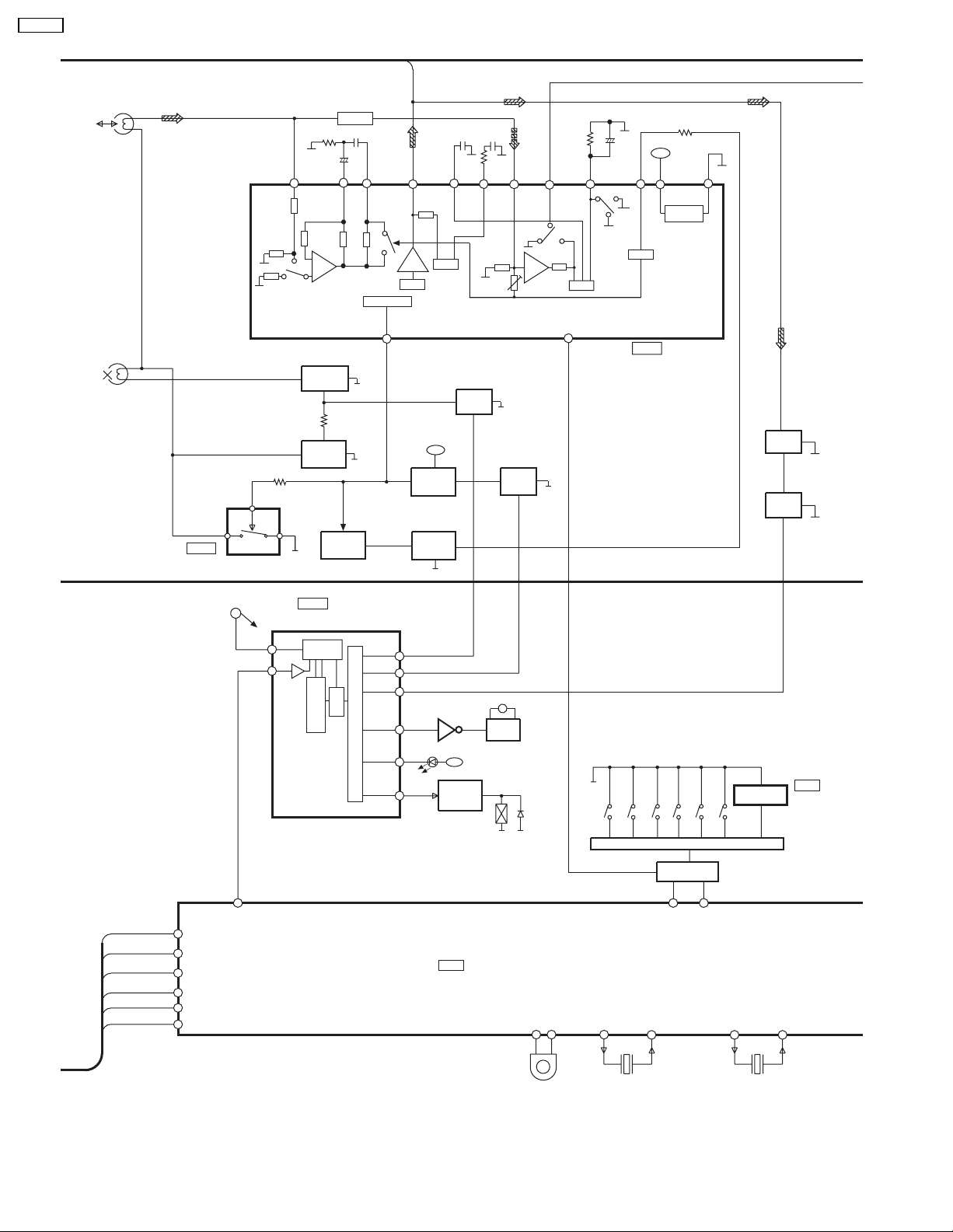
IC603
BU2090AF-E2
I/O EXPANDER 2
CONTROL
CIRCUIT
LATCH
REGISTER
12-BIT SHIFT
OUTPUT BUFFER
BP
15
14
REC_H
DMT
13
MRT_L
12
5~8
PL_L
11
C2BBGF000280
Q1314
+B
Q1315
SWITCH
MICRO-CONTROLLER
IC601
MOTOR
M
SWITCH
Q1316
SOLENOID
D1302
7
JOG1B
8
JOG1A
CR02
S1303
S1302
METAL
XCOUT
19 20
S1304
RECINH_L
Q1306,Q1307
XCIN
S1305
MODE
INTERFACE
SWITCH
2
MK_IN2
S1306
RECINH_R
3
HALF
S1307
MK_IN1
23 22
PHOTO
INTERRUPTOR
Z1001
XOUT
IC971
ON2180RLC1
(DECK 1)
XIN
A
33
SER3
30
VR601
JOG VOL
X601
X602
 Loading...