

Panasonic SA-AKX660PN, SA-AKX660PS, SA-AKX880PN, SA-AKX880PS Service manual
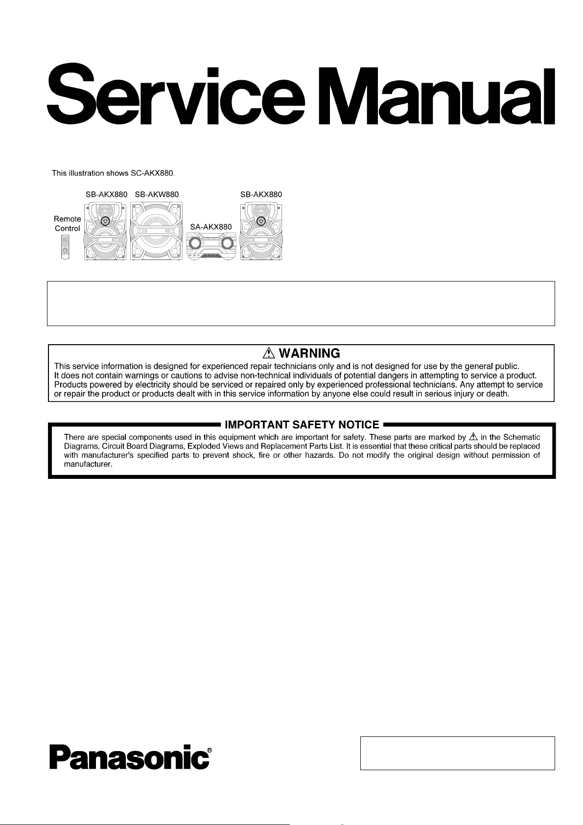
Model No. SA-AKX660PN
Product Color: (K)...Black Type
Please refer to the original service manual for:
O CD Mechanism Unit, (BRS12C) Order No. PSG1303059AE
O Speaker system SB-AKX880PNK Order No. PSG1603003CE
PSG1603002CE
CD Stereo System
SA-AKX660PS
SA-AKX880PN
SA-AKX880PS
TABLE OF CONTENTS
1 Safety Precautions----------------------------------------------- 3
1.1. General Guidelines---------------------------------------- 3
1.2. Before Repair and Adjustment ------------------------- 4
1.3. Protection Circuitry---------------------------------------- 4
1.4. Safety Parts Information --------------------------------- 5
2 Warning-------------------------------------------------------------- 6
2.1. Prevention of Electrostatic Discharge (ESD)
to Electrostatically Sensitive (ES) Devices---------- 6
2.2. Precaution of Laser Diode------------------------------- 6
2.3. General description about Lead Free Solder
(PbF)---------------------------------------------------------- 7
2.4. Handling Precautions for Traverse Unit-------------- 7
2.5. Grounding for electrostatic breakdown
prevention --------------------------------------------------- 8
3 Service Navigation----------------------------------------------- 9
3.1. Service Information --------------------------------------- 9
4 Specifications ----------------------------------------------------10
PAGE PAGE
5 Location of Controls and Components------------------ 12
5.1. Remote Control Key Button Operation ------------- 12
5.2. Main Unit Key Button Operation----------------------13
6 Service Mode ----------------------------------------------------- 14
6.1. Cold-Start --------------------------------------------------14
6.2. Sales Demonstration Lock Function ---------------- 14
6.3. Doctor Mode Table---------------------------------------15
6.4. Self-Diagnostic Mode -----------------------------------17
6.5. Self-Diagnostic Error Code Table--------------------17
7 Troubleshooting Guide ---------------------------------------19
7.1. No Power or No Display -------------------------------19
7.2. Bluetooth® Pairing Failure----------------------------- 19
7.3. No Key Function------------------------------------------19
7.4. No Remote Control Function-------------------------- 19
7.5. USB Device Cannot Detect----------------------------20
7.6. No Output Sound-----------------------------------------21
7.7. Check Point------------------------------------------------22
© Panasonic Corporation 2016. All rights reserved.
Unauthorized copying and distribution is a violation
of law.

8 Disassembly and Assembly Instructions---------------23
8.1. Types of Screws -----------------------------------------23
8.2. Disassembly Flow Chart--------------------------------24
8.3. Main Components and P.C.B. Locations-----------24
8.4. Disassembly of Top Cabinet---------------------------25
8.5. Disassembly of Front Panel Unit ---------------------25
8.6. Disassembly of Panel P.C.B.--------------------------26
8.7. Disassembly of USB P.C.B. ---------------------------26
8.8. Disassembly of Music Port P.C.B. -------------------27
8.9. Disassembly of Rear Panel----------------------------27
8.10. Disassembly of Main P.C.B.---------------------------28
8.1 1. Disassembly of CD Mechanism Unit----------------28
8.12. Disassembly of CD Interface P.C.B.-----------------30
8.13. Disassembly of Tuner P.C.B.--------------------------30
8.14. Disassembly of SMPS P.C.B.-------------------------30
9 Service Position-------------------------------------------------31
9.1. Checking of Panel P.C.B. ------------------------------31
9.2. Checking of Main P.C.B. and SMPS P.C.B. -------31
10 Block Diagram ---------------------------------------------------32
10.1. System Control -------------------------------------------32
10.2. Audio --------------------------------------------------------35
10.3. Power Supply ---------------------------------------------37
11 Wiring Connection Diagram---------------------------------40
12 Schematic Diagram---------------------------------------------42
12.1. Schematic Diagram Notes -----------------------------42
12.2. Main (CD Motor Driver) Circuit----------------------- -44
12.3. Main (USB EMMC) Circuit -----------------------------45
12.4. Main (SOC IO Expander) Circuit (1/2) --------------46
12.5. Main (SOC IO Expander) Circuit (2/2) --------------47
12.6. Main (Damp) Circuit (1/2) ------------------------------48
12.7. Main (Damp) Circuit (2/2) ------------------------------49
12.8. Main (Connector) Circuit -------------------------------50
12.9. Main (DSP) Circuit---------------------------------------51
12.10. Main (VREG Fan) Circuit (1/2)------------------------52
12.1 1 . Main (VREG Fan) Circuit (2/2)------------------------53
12.12. Main (Tuner) Circuit -------------------------------------54
12.13. SMPS Circuit (1/2) ---------------------------------------55
12.14. SMPS Circuit (2/2) ---------------------------------------56
12.15. CD Interface, USB and Music Port Circuit--------- 57
12.16. Panel Circuit-----------------------------------------------58
13 Printed Circuit Board ------------------------------------------59
13.1. Main P.C.B. (Side A)-------------------------------------59
13.2. Main P.C.B. (Side B)-------------------------------------60
13.3. SMPS P.C.B.----------------------------------------------61
13.4. Panel, USB, CD Interface and Music Port
P.C.B.--------------------------------------------------------62
13.5. Tuner P.C.B.-----------------------------------------------63
14 Vo ltage and Waveform Measurement --------------------64
14.1. Voltage Measurement-----------------------------------64
14.2. Waveform Chart ------------------------------------------68
15 Exploded View and Replacement Parts List-----------70
15.1. Cabinet Parts Location 1 -------------------------------70
15.2. Cabinet Parts Location 2 -------------------------------71
15.3. Packaging (For SC-AKX660PN/PS) ---------------- 72
15.4. Packaging (For SC-AKX880PN/PS) ---------------- 73
15.5. Mechanical Replacement Part List ------------------74
15.6. Electrical Replacement Parts List--------------------76
2
1 Safety Precautions
1.1. General Guidelines
1. IMPORTANT SAFETY NOTICE
There are special components used in this equipment which a re important for safety. These parts are marked by in the
Schematic Diagrams, Circuit Board Layout, Exploded Views and Replacement Parts List. It is essential that these critical parts
should be replaced with manufacturer’s specified parts to prevent X-RADIATION, shock, fire, or other hazards. Do not modify
the original design without permission of manufacturer.
2. An Isolation Transformer should always be used during the servicing of AC Adaptor whose chassis is not isolated from the AC
power line. Use a transformer of adequate power rating as this protects the technician from accidents resulting in personal
injury from electrical shocks. It will also protect AC Adaptor from being damaged by accidental shorting that may occur during
servicing.
3. Wh en servicing, observe the original lead dress. If a short circuit is found, replace all parts which have been overheated or
damaged by the short circuit.
4. After servicing, see to it that all the protective devices such as insulation barriers, insulation papers shields are properly
installed.
5. After servicing, make the following leakage current checks to prevent the customer from being exposed to shock hazards.
1.1.1. Leakage Current Cold Check
1. Unplug the AC cord and connect a jumper between the two prongs on the plug.
2. Measure the resistance value, with an o hmmeter, between the jumpered AC plug and each exposed metallic cabinet part on
the equipment such as screwheads, connectors, control shafts, etc. When the exposed metallic part has a return path to th e
chassis, the reading should be between 1MΩ and 5.2MΩ.
When the exposed metal does not have a return path to the chassis, the reading must be
1.1.2. Leakage Current Hot Check
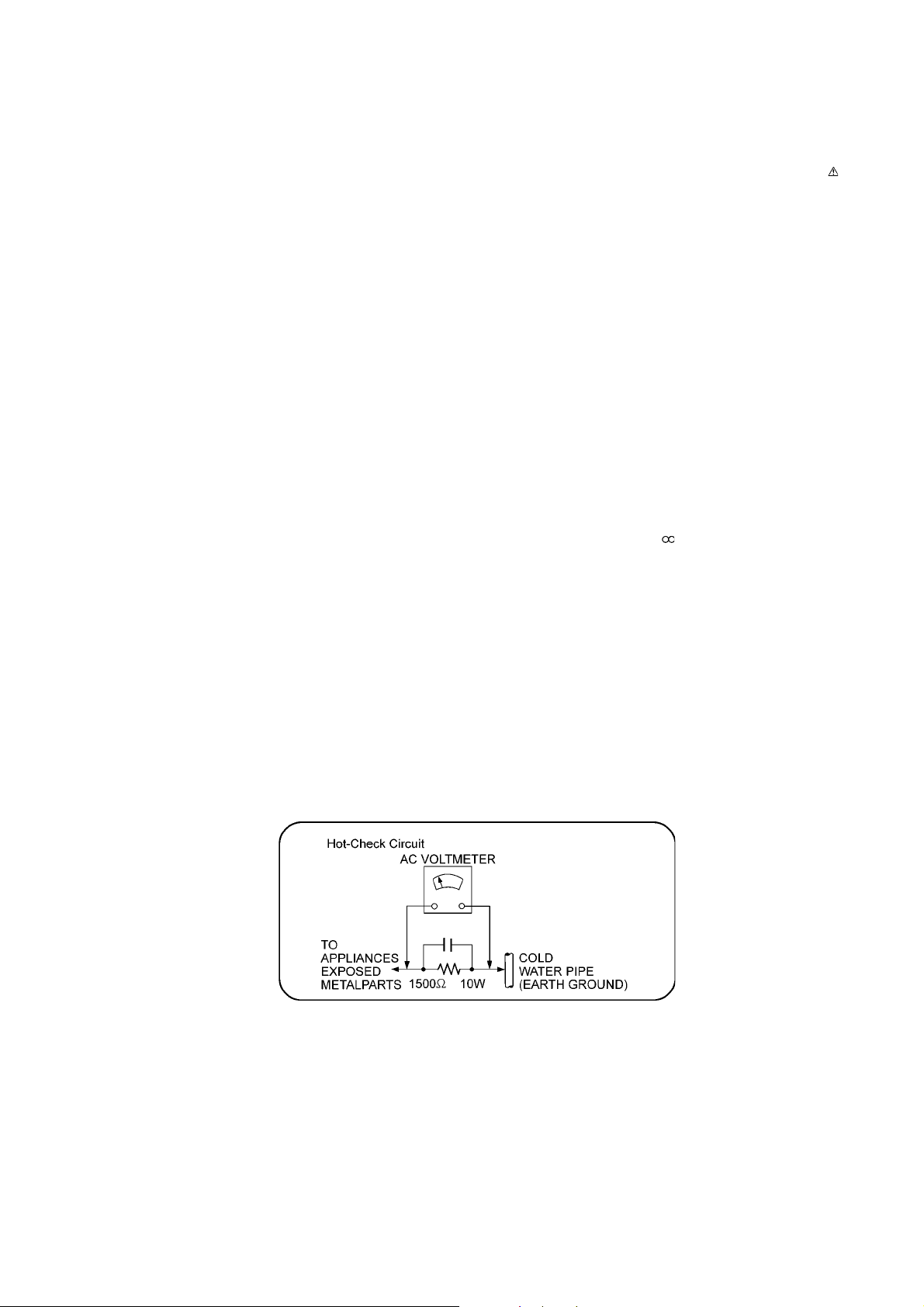
1. Plug the AC cord directly into the AC outlet. Do not use an isolation transformer for this check.
2. Connect a 1.5kΩ, 10 watts resistor, in parallel with a 0.15μF capacitors, between each exposed metallic part on the set and a
good earth ground such as a water pipe, as shown in Figure 1-1.
3. Use an AC voltmeter, with 1000 ohms/volt or more sensitivity, to measure the potential across the resistor.
4. Check each exposed metallic part, and measure the voltage at each point.
5. Reverse the AC plug in the AC outlet and repeat each of the above measurements.
6. Th e potential at any point should not exceed 0.75 volts RMS. A leakage current tester (Simpson Model 229 or equivalent)
may be used to make the hot checks, leakage current must not exceed 1/2 milliamp. In case a measurement is outside of the
limits specified, there is a possibility of a shock hazard, and the equipment should be repaired and rechecked before it is
returned to the customer.
Figure 1-1
3
1.2. Before Repair and Adjustment
Disconnect AC power to discharge AC capacitor (in SMPS P.C.B.) as indicate below diagram through a 10 Ω, 10 W resistor to
ground.
Figure 1-2
Caution:
DO NOT SHORT-CIRCUIT DIRECTLY (with a screwdriver blade, for instance), as this may destroy solid st ate devices.
After repairs are completed, restore power gradually using a variac to avoid overcurrent.
Current consumption at AC 120 V, 60 Hz in Power ON, FM Tuner at volume minimal mode should be ~ 750 mA (PN).
Current consumption at AC 220~240 V, 50/60 Hz in Power ON, FM Tuner at volume minimal mode should be ~ 750 mA (PS).
1.3. Protection Circuitry
The protection circuitry may have operated if either of the following conditions are noticed:
• No sound is heard when the power is turned on.
• Sound stops during a performance.
The function of this circuitry is to prevent circuitry damage if, for example, the positive and negative speaker connection wires are
“shorted”, or if speaker systems with an impedance less than the indicated rated impedance of the amplifier are used.
If this occurs, follow the procedure outlines below:
1. Turn off the power.
2. Determine the cause of the problem and correct it.
3. Turn on the power once again after one minute.
Note:
When the protection circuitry functions, the unit will not operate unless the power is first turned off and then on again.
4
1.4. Safety Parts Information
Safety Parts List:
There are special components used in this equipment which are important for safety.
These parts are marked by in the Schematic Diagrams, Exploded View & Replacement Parts List. It is essential that these
critical parts should be replaced with manufacturer’s specified parts to prevent shock, fire or other hazards. Do not modify the
original design without permission of manufacturer.
Safety Ref No. Part No. Part Name & Description Remarks
12 RGR0473D-AA REAR PANEL AKX660PN
12 RGR0473D-BA REAR PANEL AKX660PS
12 RGR0473E-AA REAR PANEL AKX880PN
12 RGR0473E-BA REAR PANEL AKX880PS
20 RKM0764A-K TOP CABINET
301 RAE1050Z-V TRAVERSE ASS'Y (E.S.D)
A2 K2CB2CB00022 AC CORD PN
A2 K2CQ2YY00119 AC CORD PS
A3 RQT0A60-1M O/I BOOK (Sp)
A3 RQT0A61-1B O/I BOOK (En)
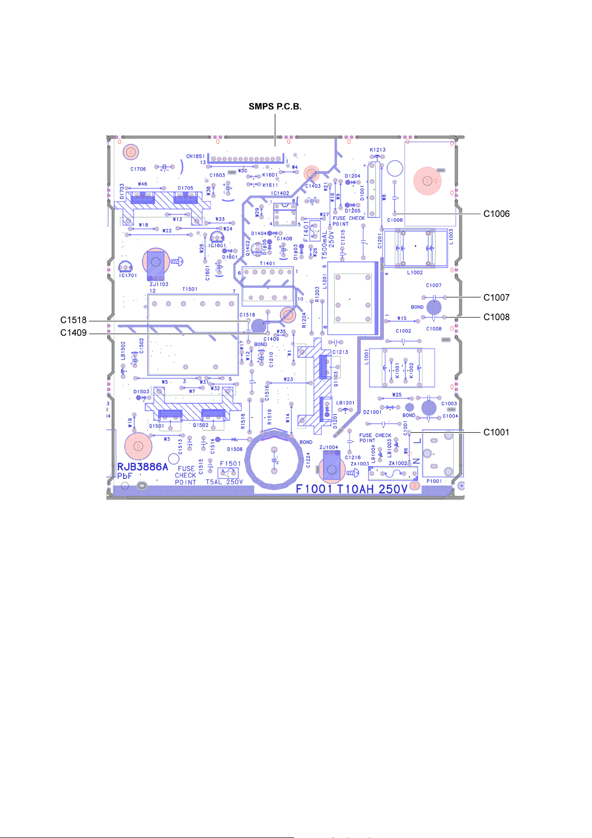
PCB7 REP5304A SMPS P.C.B (RTL) PN
PCB7 REP5304B SMPS P.C.B (RTL) PS
Q1403 B3PBA0000579 PHOTO COUPLER (E.S.D)
Q1404 B3PBA0000579 PHOTO COUPLER (E.S.D)
Q1405 B3PBA0000579 PHOTO COUPLER (E.S.D)
Q1505 B3PBA0000579 PHOTO COUPLER (E.S.D)
Q1701 B3PBA0000579 PHOTO COUPLER (E.S.D)
DZ1001 D4EAY511A127 DIODE (E.S.D)
L1002 G0B502J00005 LINE FILTER
T1401 G4DYA0000592 SWITCHING TRANSFORMER
T1501 G4DYA0000778 SWITCHING TRANSFORMER
F1001 K5D103BNA005 FUSE
F1401 K5G501YA0081 FUSE
F1501 K5G502Y00006 FUSE
P1001 K2AA2B000011 AC INLET PS
P1001 K2AB2B000007 AC INLET PN
R1001 D0GF105JA048 1M 1/4W
R1002 D0GF105JA048 1M 1/4W
R1003 D0GF105JA048 1M 1/4W
C1001 F0CAF104A105 0.1uF
C1006 F0CAF224A105 0.22uF
C1007 F1BAF471A215 470pF
C1008 F1BAF471A215 470pF
C1409 F1BAF471A215 470pF
C1518 F1BAF471A215 470pF
5
2Warning
2.1. Prevention of Electrostatic Discharge (ESD) to Electrostatically Sensi-
tive (ES) Devices
Some semiconductor (solid state) devices can be damaged easily by static electricity. Such components commonly are called Electrostatically Sensitive (ES) Devices.
The following techniques should be used to help reduce the incidence of component damag e caused by electrostatic discharge
(ESD).
1. Immediately before handling any semiconductor component or semiconductor-equipped assembly, drain off any ESD on your
body by touching a known earth ground. Alternatively, obtain and wear a commercially available discharging ESD wrist strap,
which should be removed for potential shock reasons prior to applying power to the unit under test.
2. After removing an electrical assembly equipped with ES devices, p lace the assembly on a cond ucti ve surface su ch as a luminum foil, to prevent electrostatic charge buildup or exposure of the assembly.
3. Use only a grounded-tip soldering iron to solder or unsolder ES devices.
4. Use only an anti-static solder removal device. Some solder removal devices not classified as “anti-static (ESD protected)” can
generate electrical charge sufficient to damage ES devices.
5. Do not use freon-propelled chemicals. These can generate electrical charges sufficient to damage ES devices.
6. Do not remove a replacement ES device from its protective package until immediately before you are ready to install it. (Most
replacement ES devices are packaged with leads electrically shorted together by conductive foam, aluminum foil or comparable conductive material).
7. Immediately before removing the protective material from the leads of a replacement ES device, touch the protective material
to the chassis or circuit assembly into which the device will be installed.
CAUTION:
Be sure no power is applied to the chassis or circuit, and observe all other safety precautions.
8. Minimize bodily motions when handling unpackaged replacement ES devices. (Otherwise harmless motion such as the
brushing together of your clothes fabric or the lif ting of your foot from a carpeted floor can generate static electricity (ESD) sufficient to damage an ES device).
2.2. Precaution of Laser Diode
Caution:
This product utilizes a laser diode with the unit turned “on”, invisible laser radiation is emitted from the pickup lens.
Wavelength: 790 nm (CD)
Maximum output radiation power from pick up : 10 0 μW/VDE
Laser radiation from the pickup unit is safety level, but be sure the followings:
1. Do not disassemble the pickup unit, since radiation from exposed laser diode is dangerous.
2. Do not adjust the variable resistor on the pickup unit. It was already adjusted.
3. Do not look at the focus lens using optical instruments.
4. Recommend not to look at pickup lens for a long time.
6
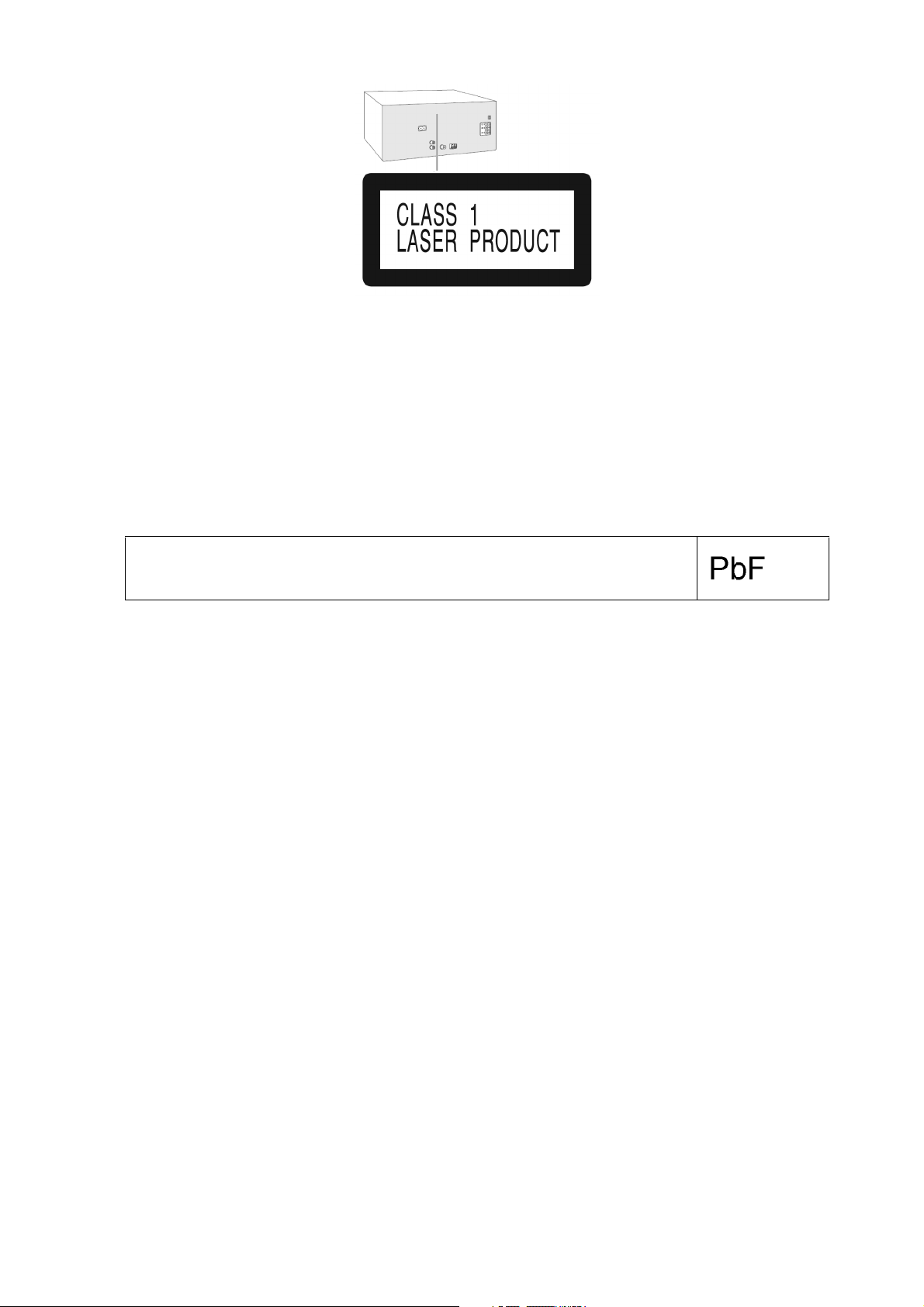
Figure 2-1
2.3. General description about Lead Free Solder (PbF)
The lead free solder has been used in the mounting proce ss of a ll electrical components on the printed circuit board s used for this
equipment in considering the globally environmental conservation.
The normal solder is the alloy of tin (Sn) and lead (Pb). On the other hand, the lead free solder is the alloy ma inly consists of tin
(Sn), silver (Ag) and Copper (Cu), and the melting point of the lead free solder is higher approx.30 degrees C (86°F) more than that
of the normal solder.
Definition of PCB Lead Free Solder being used
The letter of “PbF” is printed either foil side or components side on the PCB using the lead free solder.
(See right figure)
Service caution for repair work using Lead Free Solder (PbF)
• The lead free solder has to be used when repairing the equipment for which the lead free solder is used.
(Definition: The letter of “PbF” is printed on the PCB using the lead free solder.)
• To put lead free solder, it should be well molten and mixed with the original lead free solder.
• Remove the remaining lead free solder on the PCB cleanly for soldering of the new IC.
• Since the melting point of the lead free solder is higher than that of th e normal lead solder, it takes the longer time to melt the
lead free solder.
• Use the soldering iron (more than 70W) equipped with the temperature con trol after setting the temperatu re at 350±30 degrees
C (662±86°F).
Recommended Lead Free Solder (Service Parts Route.)
• The following 3 types of lead free solder are available through the service parts route.
RFKZ03D01K-----------(0.3mm 100g Reel)
RFKZ06D01K-----------(0.6mm 100g Reel)
RFKZ10D01K-----------(1.0mm 100g Reel)
Note
* Ingredient: tin (Sn), 96.5%, silver (Ag) 3.0%, Copper (Cu) 0.5%, Cobalt (Co) / Germanium (Ge) 0.1 to 0.3%
2.4. Handling Precautions for Traverse Unit
The laser diode in the optical pickup unit may break down due to static electricity of clothes or human b ody. Special care must be
taken avoid caution to electrostatic breakdown when servicing and handling the laser diode in the traverse unit.
2.4.1. Cautions to Be Taken in Handling the Optical Pickup Unit
The laser diode in the optical pickup un it may be damaged due to electrostatic discharge generating from clothes or human body.
Special care must be taken avoid caution to electrostatic discharge damage when servicing the laser diode.
1. Do not give a considerable shock to the optical pickup unit as it has an extremely high-precise structure.
2. To prevent the laser diode from the electrostatic discharge damage, the flexible cable of the optical pickup unit removed
should be short-circuited with a short pin or a clip.
3. The flexible cable may be cut off if an excessive force is applied to it. Use caution when handling the flexible cable.
4. The antistatic FFC is connected to the new optical pickup unit. After replacing the optical pickup unit and connecting the flexi-
7
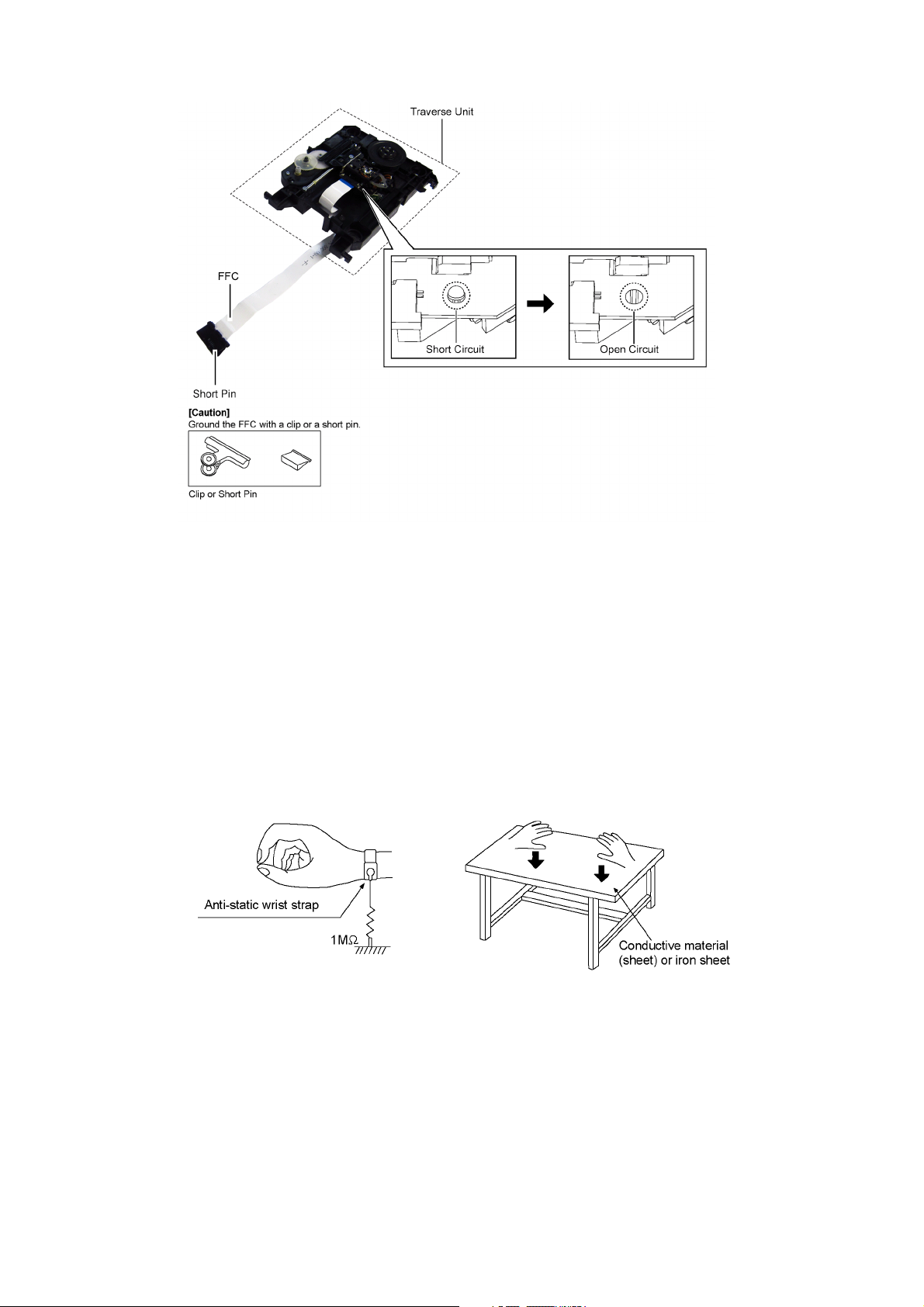
ble cable, cut off the antistatic FFC.
Figure 2-2
2.5. Grounding for electrostatic breakdown prevention
• As for parts that use optical pick-up (laser diode), the optical pick-up is destroyed by the static electricity of the working environment.
Repair in the working environment that is grounded.
2.5.1. Worktable grounding
• Put a conductive material (sheet) or iron sheet on the area where the optical pickup is placed and ground the sheet.
2.5.2. Human body grounding
• Use the anti-static wrist strap to discharge the static electricity form your body (Figure 2-3).
Figure 2-3
8

3 Service Navigation
UPDATE PROCEDURE
Perform the following steps.
Ɣ Step 1: Preparing USB devic
e
Ɣ Step 2: Software Update
Step 1: Preparing USB device
Before start creating the update USB, it is nessesary to check the update file.
It is important to use the correct file otherwise USB version up process will not
working.
Note: Please do not rename the file as the updating process will look for above naming. If different
name, version up process will not work.
To create USB update, copy the desired FRM file (depends on model) into USB device.
Please make sure there is no other files inside the USB device.
Step 2: Software Update
<Caution>
Ź During the update process, do not disconnect the AC power supply cord.
Ź Do not press any buttons, except as instructed. Failure to do so may result in the set
becoming unresponsive which will require repair.
Step:
Ź Set need to be turn ON in order to support USB update process.
Ź Go to USB selector until the display show "NODEVICE".
1. Insert USB device (With FRM file inside)
2. During the update process, the below message will shown on the display.
3. When "SUCCESS" display appear, unplug USB then ac out supply. Firmware updation process
completed.
Thisistheprecentageof
theupdateprocess.It
willstartwith0%until
99%
3.1. Service Information
This service manual contains technical information which will allow service personnel’s to understand and service this model.
Please place orders using the parts list and not the drawing reference numbers.
If the circuit is changed or modified, this information wil l be fol lowed by supplemen t service manual to be filed with original se rvice
manual.
3.1.1. Software Update Procedure
9

4 Specifications
Q Amplifier section
RMS output power stereo mode
Front Hi (both ch driven) 350 W per channel (3 Ω),
1 kHz, 30% THD (for AKX660)
350 W per channel (3 Ω),
1 kHz, 30% THD (for AKX880)
Front Lo (both ch driven) 500 W per channel (2 Ω),
100 Hz, 30% THD
(for AKX660)
500 W per channel (2 Ω),
100 Hz, 30% THD
(for AKX880)
Subwoofer Ch (for AKX880) 500 W per channel (2 Ω),
100 Hz, 30% THD
Total RMS stereo mode power 1700 W (for AKX660)
2200 W (for AKX880)
Q Tuner, terminals section
Preset memory FM 30 stations
AM 15 stations
Frequency modulation (FM)
Frequency range 87.5 MHz to 108.0 MHz
(100 kHz step) (for PN)
87.9 MHz to 107.9 MHz
(200 kHz step) (for PN)
87.50 MHz to 108.00 MHz
(50 kHz step) (for PS)
Antenna terminals 75 Ω (unbalanced)
Media file format support MP3 (*.mp3)
Memory recording
Bit rate 128 kbps
Memory recording speed 1x, 3x (CD only)
Recording file format MP3 (*. Mp3)
®
Q Bluetooth
Version
Class Class 2
Supported profiles A2DP, AVRCP, SPP OPP, FTP
Operating frequency 2.4 GHz band, FH-SS
Operating distance 10 m line of sight
Q General
Power supply AC 120 V, 60 Hz (for PN)
Power consumption 173 W
Dimensions (W x H x D) 348 mm x 193 mm x 251 mm
Mass 3.6 kg
Operating temperature range 0 °C to +40 °C
section
®
Bluetooth
AC 220 to 240 V, 50/60 Hz
Ver.2.1 + EDR
(for PS)
Amplitude modulation (AM)
Frequency range 520 kHz to 1710 kHz
(10 kHz step) (for PN)
522 kHz to 1629 kHz
(9 kHz step) (for PS)
520 kHz to 1630 kHz
(10 kHz step) (for PS)
AUX 1
Audio input Pin jack (1 system)
AUX 2
Sensitivity 100 mV, 4.7 k Ω
Q Disc section
Discs played (8 cm or 12 cm) CD, CD-R/RW (CD-DA, MP3*)
* MPEG-1 Layer 3
Pick up
Wavelength 790 nm (CD)
Q USB section
USB Port
USB standard USB 2.0 full speed
Media file format support MP3 (*.mp3)
USB device file system FAT12, FAT16, FAT32
USB recording
Bit rate 128 kbps
USB recording speed 1x, 3x (CD only)
Recording file format MP3 (*.mp3)
Q Internal memory section
Memory
Memory size 4 GB
Operating humidity range 35% to 80% RH
(no condensation)
Power Consumption in standby
mode (approximate)
Power Consumption in standby
mode (approximate)
(With "BLUETOOTH STANDBY" set
to "ON")
Note:
1. Specifications are subject to change without notice.
Mass and dimension are appropriate
2. Total harmonic distortion is measured by the digital spectrum
analyzer.
Q System: SC-AKX660PNK
Main Unit: SA-AKX660PNK
Speakers: SB-AKX880PNK
Q System: SC-AKX660PSK
Main Unit: SA-AKX660PSK
Speakers: SB-AKX880PNK
Q System: SC-AKX880PNK
Main Unit: SA-AKX880PNK
Speakers: SB-AKX880PNK
Subwoofer: SB-AKW880PNK
Q System: SC-AKX880PSK
Main Unit: SA-AKX880PSK
Speakers: SB-AKX880PNK
Subwoofer: SB-AKW880PNK
0.3 W (for PN)
0.4 W (for PS)
0.4 W (for PN)
0.6 W (for PS)
10
5 Location of Controls and Components
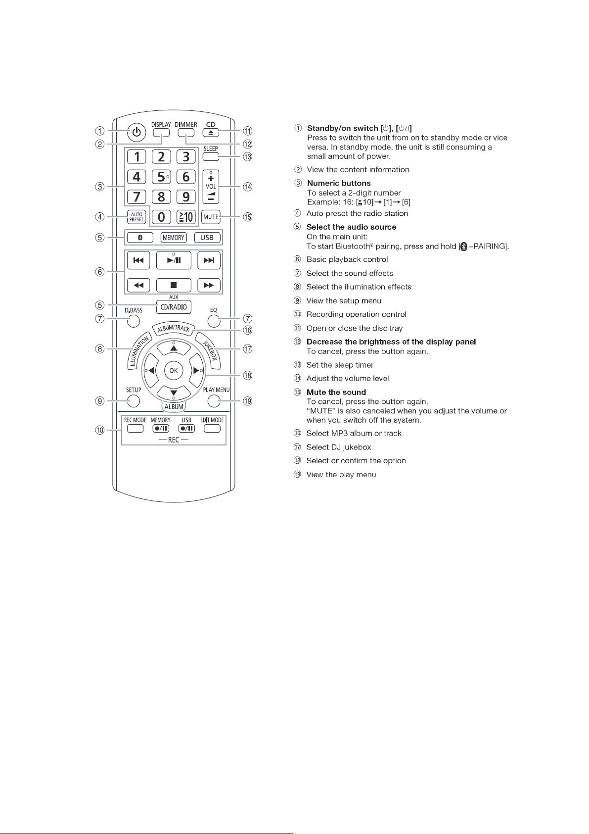
5.1. Remote Control Key Button Operation
11
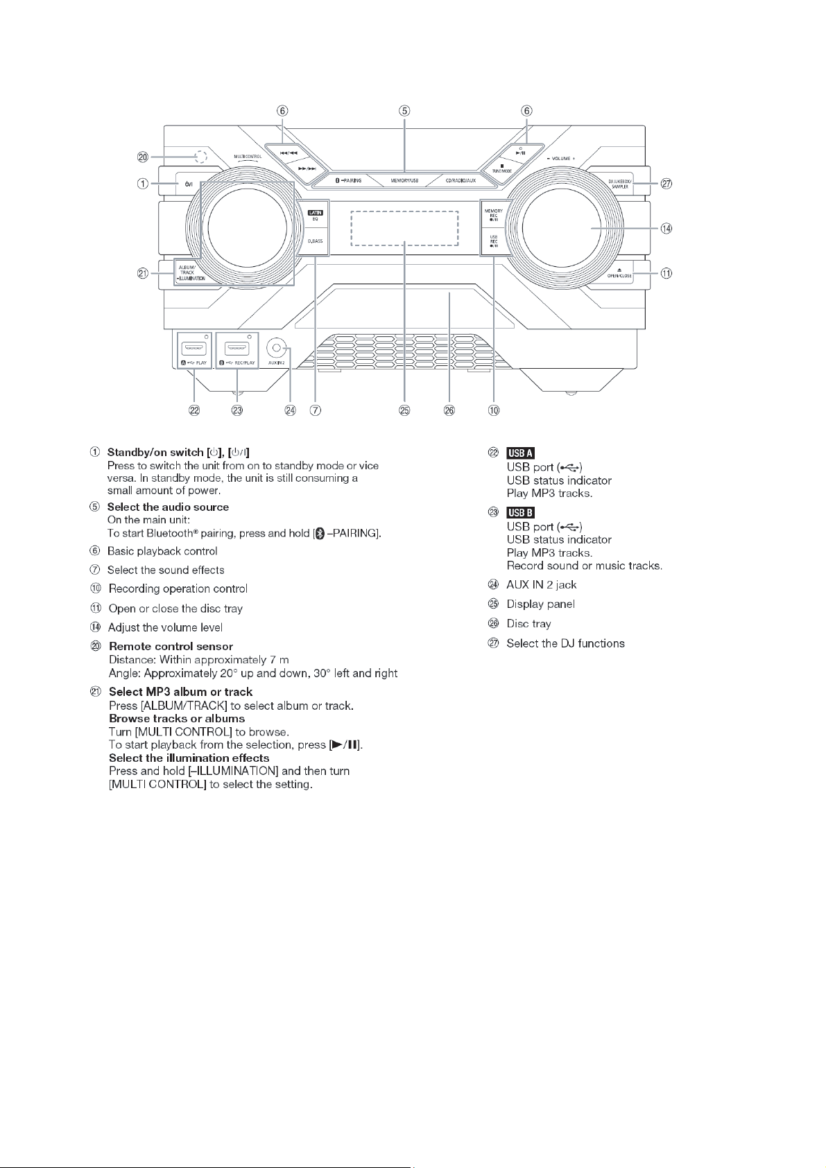
5.2. Main Unit Key Button Operation
12
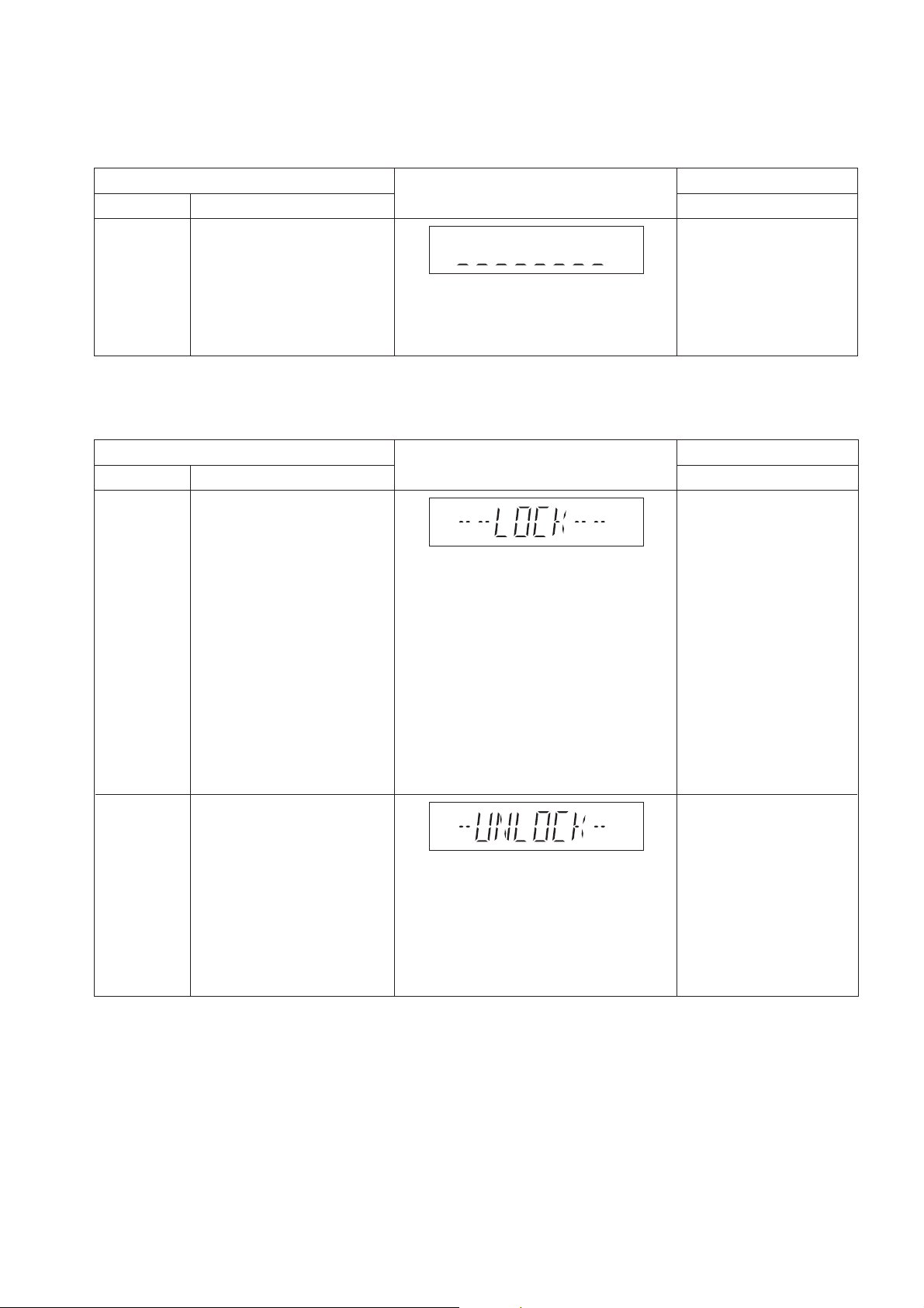
6 Service Mode
FL Display
Key Operation
Front Key
Item
DescriptionMode Name
Cold Start
To carry out cold-start or initialize
to shipping mode
1. Unplug AC power cord.
2. Press & hold [POWER]
button.
3. Plug in AC power cord
while [POWER] button
being pressed.
4. Release [POWER] button.
Entering into
Sales
Demonstration
Lock Mode
To enter into sales demonstration
lock mode.
1. Turn on the unit.
2. Select to any mode
function.
3. Press and hold
[;OPEN/CLOSE] and
[CD/RADIO/AUX] keys for
5 sec or more.
The display will show upon
entering into this mode for
2 sec.
Note: [;OPEN/CLOSE]
button is invalid and the main
unit displays "LOCKED" while
the lock function mode is
entered.
Cancellation of
Sales
Demonstration
Lock Mode
To cancel sales demonstration
lock mode.
1. Turn on the unit.
2. Select to CD mode function.
3. Set volume to Vol 19.
4. Press and hold
[;OPEN/CLOSE] and
[CD/RADIO/AUX] keys for
5 sec or more.
The display will show upon
entering into this mode for
2 sec.
FL Display
Key Operation
Front Key
Item
DescriptionMode Name
6.1. Cold-Start
6.2. Sales Demonstration Lock Function
13
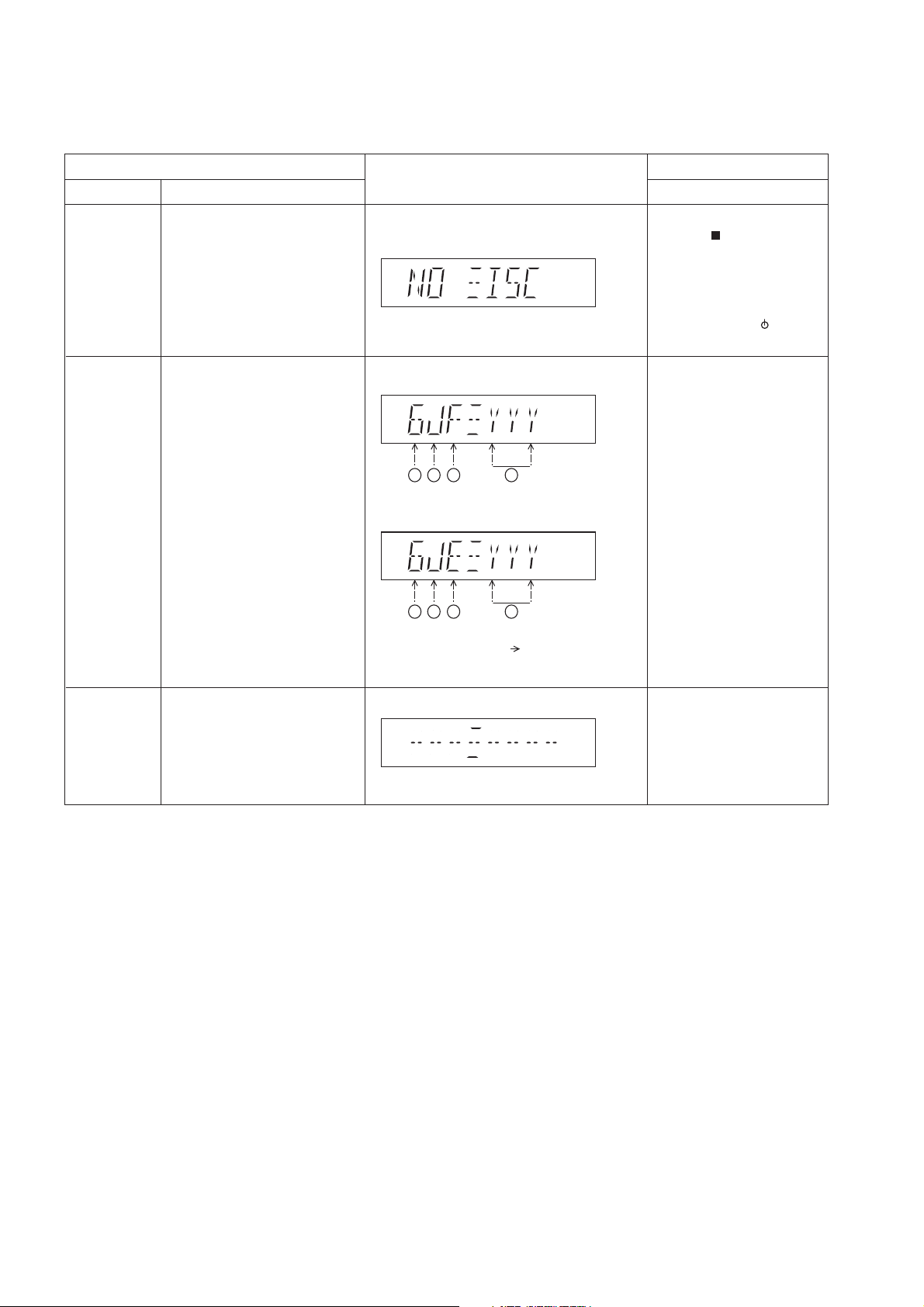
6.3. Doctor Mode Table
FL Display
Key Operation
Front Key
Item
DescriptionMode Name
Doctor Mode
EEPROM
checksum
check
(For AKX660)
(Decimal)
1 2 3 4
To enter into Doctor Mode In CD Mode:
1. Press [ ] button on
main unit follow by [4]
and [7] on remote control.
In CD mode:
1. Enter into Doctor Mode
2. To exit, press [SLEEP]
button on remote control or,
press [POWER, /I] button
on Main Unit
Displaying of
1. Year Develop.
2. Model Type.
3. ROM Type.
4. Firmware Version.
(For AKX880)
Cold Start
To active cold start upon next AC
power up when reset start is
execute the next time.
In Doctor Mode:
1. Press [4] button on the
remote control.
Version No. (001 ~ 999) specific for each
firmware
(Decimal)1 2 3 4
6.3.1. Doctor Mode Table 1
14
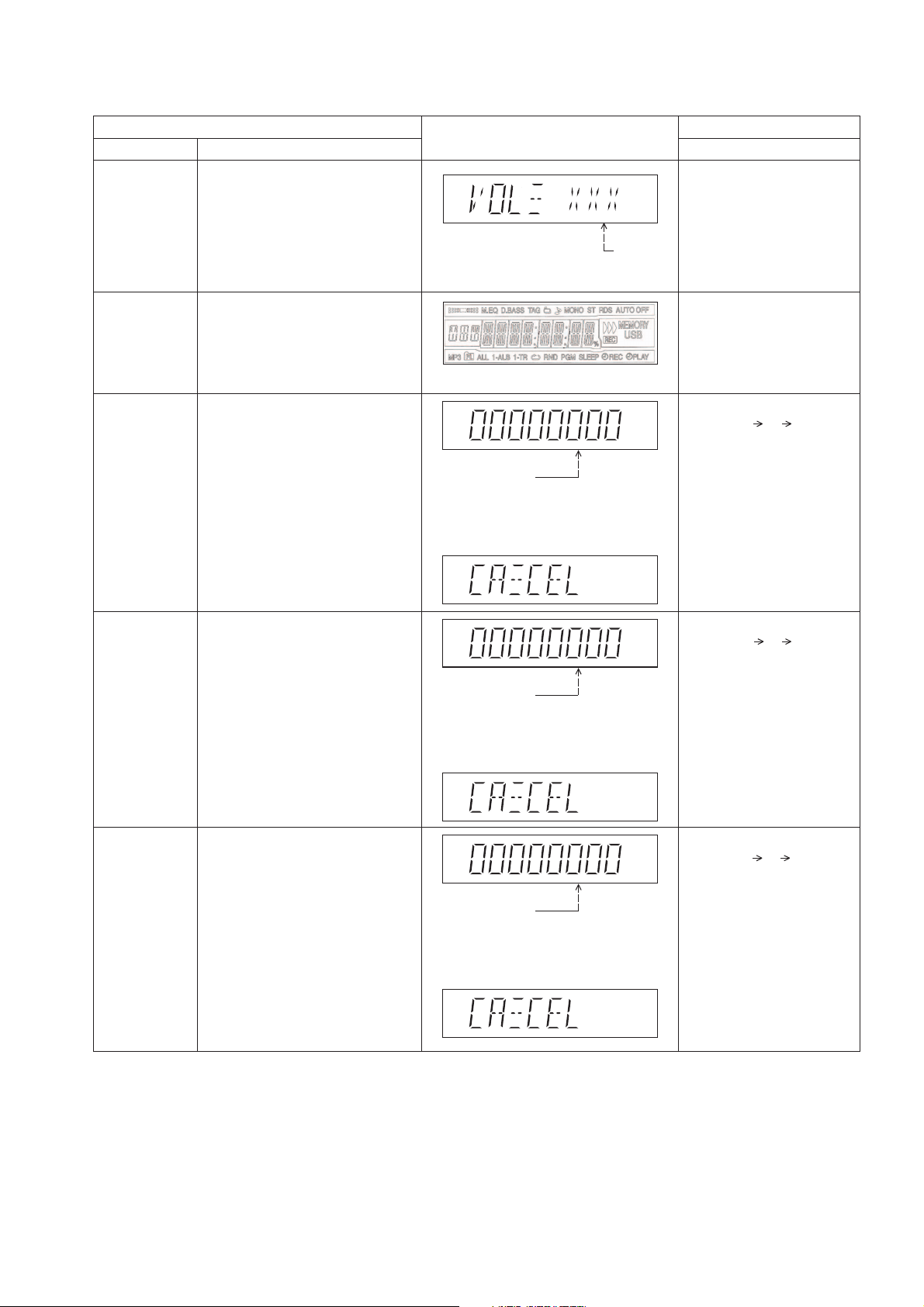
6.3.2. Doctor Mode Table 2
FL Display
Key Operation
Front Key
Item
DescriptionMode Name
Volume Setting
Check
FL Display Check
To check volume setting of the main
unit.
To check FL segment display.
All segments will light up while all LED
blink at 0.5s intervals.
In Doctor Mode:
1. Press [7], [8], [9] button on
the remote control.
In Doctor mode:
1. Press [1] button on the
remote control.
2. To cancel this mode, press
[0] button on the remote
control.
Press [7]: VOL50
Press [8]: VOL35
Press [9]: VOL0
Volume
In this mode, the tray will open & close
automatically.
Cancellation Display
Loading Test To determine open & close
operation of the CD Mechanism Unit.
The counter will
increment by one.
When reach 99999999
will change to 00000000
Cancellation Display
Traverse Test To determine traverse unit
operation for inner & outer access track.
The counter will
increment by one.
When reach 99999999
will change to 00000000
The counter will
increment by one.
When reach 99999999
will change to 00000000
Cancellation Display
Reliability Test
(Combination)
In this mode, ensure the CD is in the
main unit.
To determine traverse unit
operation & open/close operation of the
mechanism.
In this mode, ensure the CD is in the
main unit.
In Doctor Mode:
1. Press [10] [2] [1] button
on the remote control.
In Doctor Mode:
2. To cancel this mode, press
[0] button on the remote
control.
2. To cancel this mode, press
[0] button on the remote
control.
2. To cancel this mode, press
[0] button on the remote
control.
1. Press [10] [1] [2] button
on the remote control.
In Doctor Mode:
1. Press [10] [1] [5] button
on the remote control.
15
6.4. Self-Diagnostic Mode
FL Display
Key Operation
Front Key
Item
DescriptionMode Name
Self Diagnostic
Mode
edomDCtceleS:1petSgnikcehccitsongaidflesotniretneoT
(Ensure no disc is inserted).
To exit, press [ I] on main unit or
remote control.
Step 2: Press & hold [ ] button
follow by [ //] on
main unit for 2 seconds.
Error Code
Information
System will perform a check on
any unusual/error code from the
memory
,edomcitsongaidflesnI:1petS:elpmaxE
Press [ ] on main unit.
Delete error code To clear the stored in memory
(EEPROM IC)
Step 1: In self diagnostic mode,
Press [OK] on remote
control for 5 seconds.
To exit, press [ I] on main unit or
remote control.
/
Solution
(PCB exchange repair)
FL Display
Key Operation
Front Key
Item
DescriptionMode Name
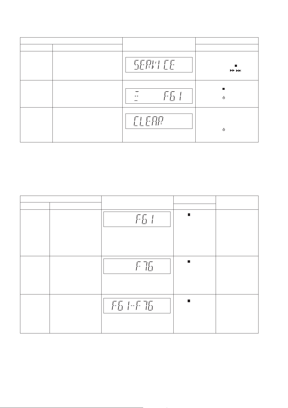
Error Code F61 Diagnosis Contents:
Power Amp IC output
abnormal.
Upon power on,
PCONT=HIGH,
DC_DET_AMP after
checking LSI.
Error Code F76 Diagnosis Contents:
Power Amp IC output
abnormal.
DC_DET_PWR.
Error Code
F61-76
Diagnosis Contents:
Power Amp IC output
abnormal.
Both DCDET (NG).
Press [ ] on main unit
for next error.
Press [ ] on main unit
for next error.
Press [ ] on main unit
for next error.
Check main (IC6000).
Check SMPS P.C.B.
(Main IC1002 / IC1003).
DAMP and power
supply abnormal.
6.5. Self-Diagnostic Error Code Table
Self-Diagnostic Function provides information on any problems occurring for the un it and its respective components by displaying
the error codes. These error code such as U**, H** and F** are stored in memory and held unless it is cleared.
The error code is automatically display after entering into self-diagnostic mode.
6.5.1. Power Supply Error Code Table
16
6.5.2. CD Mechanism Error Code Table
Solution
(PCB exchange repair)
FL Display
Key Operation
Front Key
Item
DescriptionMode Name
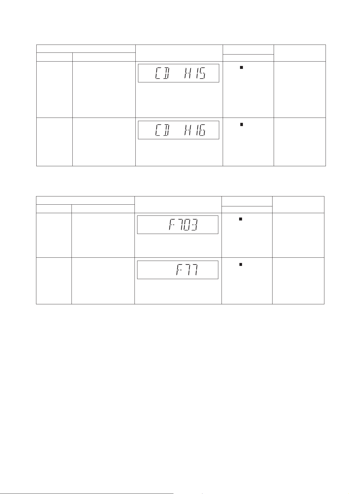
Error Code
CD H15
Diagnosis Contents:
CD Open Abnormal
.
During operation
POS_SW_R On fail to be
detected within 4 sec.
Error No. shall be clear
by force or during cold start.
Error Code
CD H16
Diagnosis Contents:
CD Closing Abnormal
.
During operation
POS_SW_CEN
On fail to be
detected within
Error No. shall be clear by
force
Press [ ] on main unit
for next error.
Press [ ] on main unit
for next error.
4 sec.
Check following:
1. CD Interface P.C.B.
(Pin 3, 4, 6)
2. SOC IC (IC1001)
Check following:
1. CD Interface P.C.B.
(Pin 6, 3, 4)
2. SOC IC (IC1001)
Solution
(PCB exchange repair)
FL Display
Key Operation
Front Key
Item
DescriptionMode Name
Error Code
F703
Diagnosis Contents:
Bluetooth Communication.
Communication between
Bluetooth module and
micro-p abnormal.
Error Code F77 Diagnosis Contents:
Bluetooth Address Error
If there is no valid Bluetooth
address stored in the
EEPROM IC.
Press [ ] on main unit
for next error.
Press [ ] on main unit
for next error.
Check following:
1. Bluetooth P.C.B.
2. SOC IC on Main
P.C.B.
Check following:
1. EEPROM IC
(IC1004) on Main
P.C.B.
6.5.3. Bluetooth Error Code Table
17
7 Troubleshooting Guide
7.1. No Power or No Display
Press Power Button
of Unit or Remote Control
to Turn ON the Unit
Check Secondary Cap. (C7)
DAMP VCC: 38
[refer to check point ]
4 -
NG
Check capacitor, C7
7.2. Bluetooth
Press Power Button
of Unit or Remote Control
to Turn ON the Unit
Caution:
No Display on
FL Panel
1. AC Cord Plug-out
2. Check Fuse(F1) = 0 ohm
[ refer to check point - ]
11
NG
Check AC Cord
& Fuse
OKOK OK OK OK
4
Check Regulator IC
(IC2108)
Measured 3.3V at Pin 2
[refer to check point ]
5
NG
Check IC2108
®
Pairing Failure
Press [PAIRING] on the Set
or Remote Control
Display "BLUETOOTH"
Check Regulator IC
(IC2101)
Measured 5.6V at C2155
[refer to check point ]
GGNN
Check IC2101
"PAIRING' will display and
blinking while handphone or other
devices are Connecting to the Set
option 1
NG
Do the Cold Start
AC Plug-out. Press and Hold
Power Button then
AC Plug-IN, wait to display "-------"
then will OFF the Set, back to start.
NG
option 2
Check Main P.C.B &
BT P.C.B
Check Primary E-Cap (C2)
Measured 300V or more
[refer to check point - ]
2
NG
Check Capacitor, C2
Check Connector (CN2506)
Measured 5/3.3/12/V
6
[refer to check point ]
Check FFC connection
2
at Pin 5-8
GN
& voltage
The set will displayed the
"READY" followed
by "BLUETOOTH"
NG
Change Main PCB or
BT P.C.B
Check Secondary Cap. (C6)
KOKO
or Back up 5V voltage
[refer to check point - ]
7
3 3
NG
Check Capacitor, C6
If No Display on
KKOOKO
No Problem
FL Panel
Check Panel
P.C.B
Found
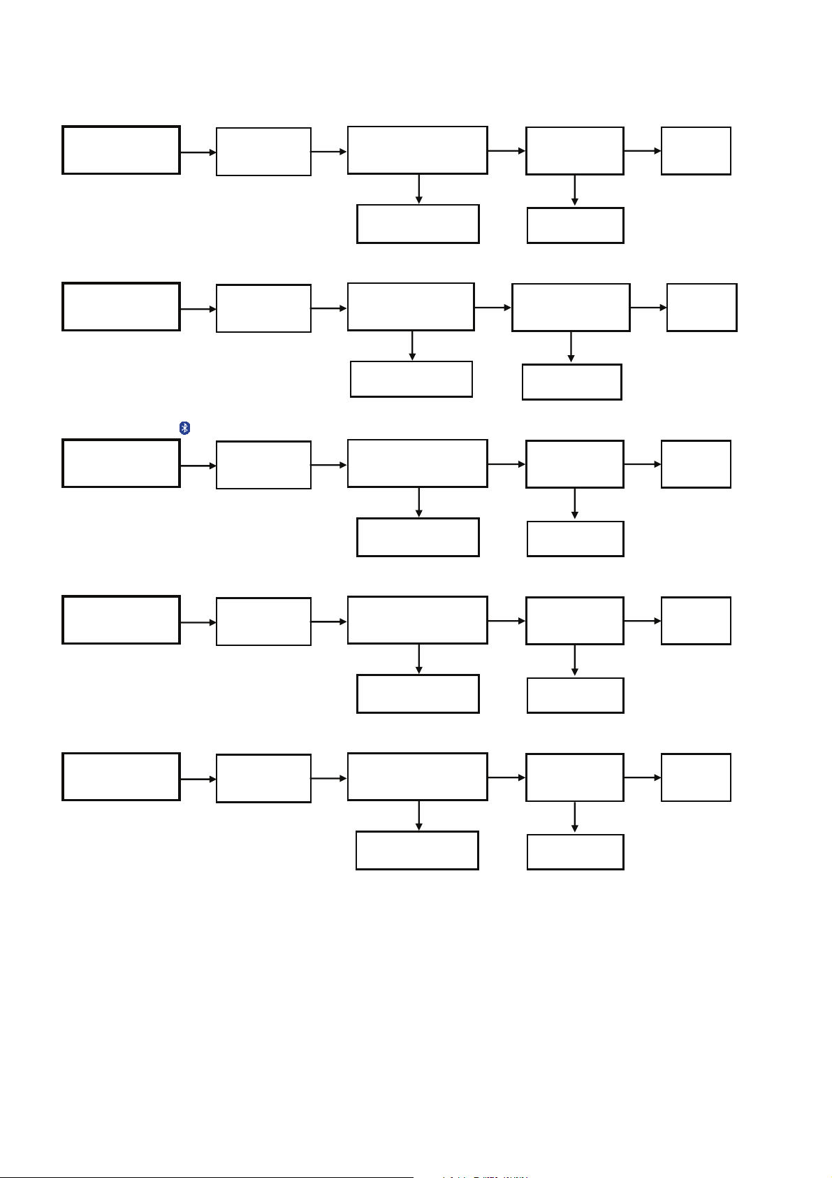
7.3. No Key Function
Press Power Button
or CD Door Open of Unit
to Turn ON the Unit
If Cannot
Power ON
(No Display)
Use Remote Control
to Turn ON the Set
NG
Check Main PCB
OK
7.4. No Remote Control Function
Press the Remote Control
Power Button
to Power ON the Unit
(Ensure have Battery & New)
If Cannot
Power ON
(No Display)
Press the Power Button
of the Unit
to Turn ON the Set
NG
Check Regulator IC
(IC2108)
Measured 3.3V at Pin # 2
[refer to check point ]
NG
Check IC2108
OK
5
FL Display
Show "HELLO"
FL Display
Show "HELLO"
OK
OK
Press the Power Buttons
or Other Buttons
NG
Check and Ensure that
Panel Connector is
Properly Insert
NG
If Buttons are not Working
Check Panel PCB
Press Remote
Control Buttons
NG
Check Panel P.C.B
OK
OK
All Remote Control
Buttons are Working
All Buttons
are Working
OK
OK
No Problem Found
No Problem Found
18

7.5. USB Device Cannot Detect
Press Power Button
of Unit or Remote Control
to Turn ON the Unit
Press [USB/CD] on the Set or
Remote Control to
Select USB A or B, Display
"USB A/B" and "NO DEVICE"
Plug-in USB Device to USB port
with Red LED indicated
(e.g. USB B) FL Display " USB B"
NG
USBB_5V at CN2511 pin #7
(USBA_5V at pin # 6)
[refer to check point
8
]
NG
Change FFC Connection,
USB , Main PCB
Press Play
FL Display
"Music Name or Title"
NG
Check Main PCB and
Panel P.C.B
KKOOKO
No Problem
Found
19
7.6. No Output Sound
CD Play
USB Play
Bluetooth Play
Tuner Mode
MEMORY Mode (AKX660 only)
Press Power Button
of Unit or Remote Control
to Turn ON the Unit
Check Speaker
Output at Main P.C.B
NG
Press Play
FL Display "Track & Count"
NG
Output Sound
No Problem
Found
KOKOKO
CD Mode
Check CD Mechanism
of Unit or Remote Control
to Turn ON the Unit
Check Speaker Output
at Main PCB
NG
Insert USB Thumdrive
FL Display "USB A/B"
Press "Play"
NG
Output Sound
No Problem
Found
OK KOKO
USB Mode
Check USB Thumdrive
and USB P.C.B
of Unit or Remote Control
to Turn ON the Unit
Check Speaker Output
at Main PCB
NG
Press Play
FL Display "BLUETOOTH "
NG
Output Sound
No Problem
Found
OK OK OK
Bluetooth Mode
Re-connect Bluetooth
into the Device
of Unit or Remote Control
to Turn ON the Unit
Change FFC, Speaker
O/P at Main PCB
NG
Search for Tuner Signal
NG
Output Sound
No Problem
Found
KOKOKO
FM/AM Mode
Check the Antenna
Wire Connection, Tuner IC
of Unit or Remote Control
to Turn ON the Unit
Check Memory IC
at Main PCB
NGNG
Output Sound
No Problem
Found
OK OK OK
MEMORY Mode
Press Play
FL Display "Track & Count"
Check Speaker output
at Main PCB
Press Power Button
Press Power Button
Press Power Button
Press Power Button
20
7.7. Check Point
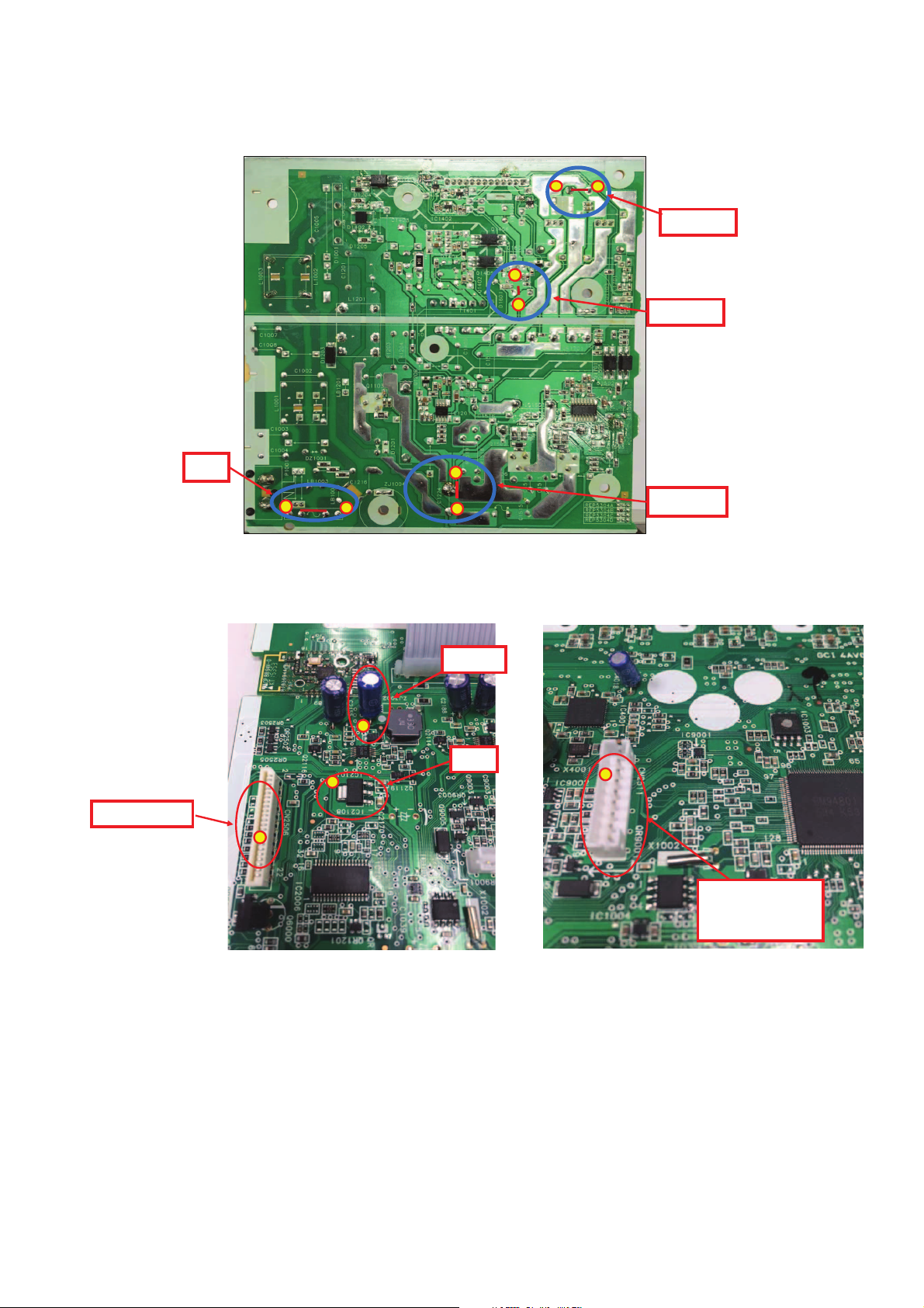
Fuse (F1)
(0 ohm)
11
2
2
Pri. Cap (C2)
(300V or more)
3
3
Sec. Cap. C6
(5V)
Sec. Cap. C7
(39V)
4
4
5
6
C2108
(3.3V)
C2155
5V
7
CN2506_Pin 5- 8
5V/3.3V/12V
8
CN2511
Pin #6 (USB-A)
/Pin #7 (USB-B)
5V
7.7.1. SMPS P.C.B.
7.7.2. Main P.C.B.
21
8 Disassembly and Assembly Instructions
• Illustration is based on SA-AKX880PN/PS.
Caution Note:
• This section describes the disassembly and/or assembly procedures for all major printed circuit boards & main components for the unit. (You may refer to the section of “Main components and P.C.B Locations” as described in the service
manual)
• Before carrying out the disassembly process, please ensure all the safety precautions & procedures are followed.
• During the disassembly and/or assembly process, please handle with care as there may be chassis components with
sharp edges.
• Avoid touching heatsinks due to its high temperature after prolong use. (See caution as described below)
• During disassembly and assembly, please ensure proper service tools, equipments or jigs is being used.
• During replacement of component parts, please refer to the section of “Replacement Parts List” as described in the service manual.
• Select items from the following indexes when disassembly or replacement are required.
• Disassembly of Top Cabinet
• Disassembly of Front Panel Unit
• Disassembly of Panel P.C.B.
• Disassembly of USB P.C.B.
• Disassembly of Music Port P.C.B.
• Disassembly of Rear Panel
• Disassembly of Main P.C.B.
• Disassembly of CD Mechanism Unit
• Disassembly of CD Interface P.C.B.
• Disassembly of Tuner P.C.B.
• Disassembly of SMPS P.C.B.
8.1. Types of Screws
22
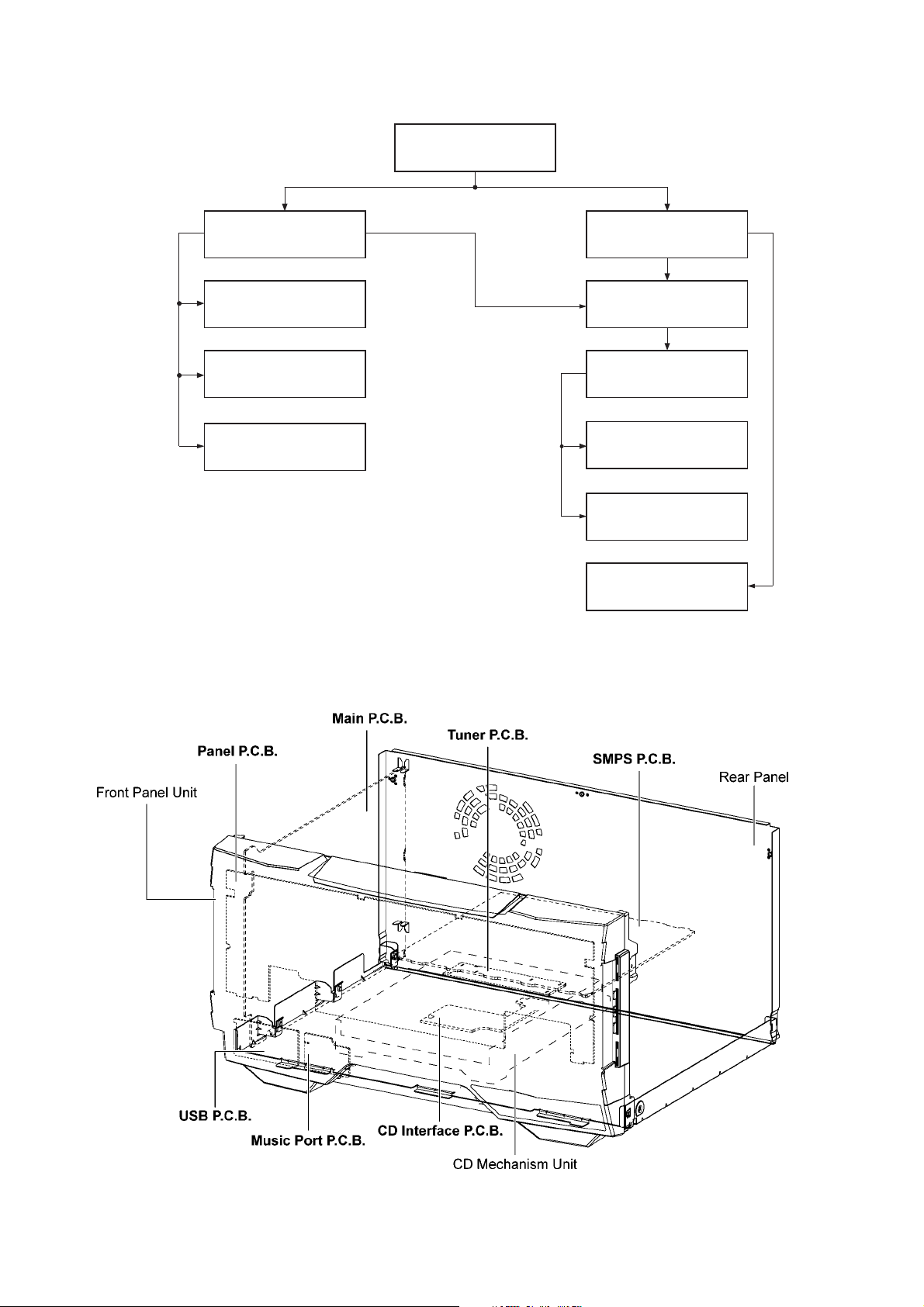
8.2. Disassembly Flow Chart
Top Cabinet
Front Panel Unit
Panel P.C.B.
USB P.C.B.
Music Port P.C.B.
8.3. Main Components and P.C.B. Locations
Rear Panel
Main P.C.B.
CD Mechanism
Unit
CD Interface
P.C.B.
Tuner P.C.B.
SMPS P.C.B.
23
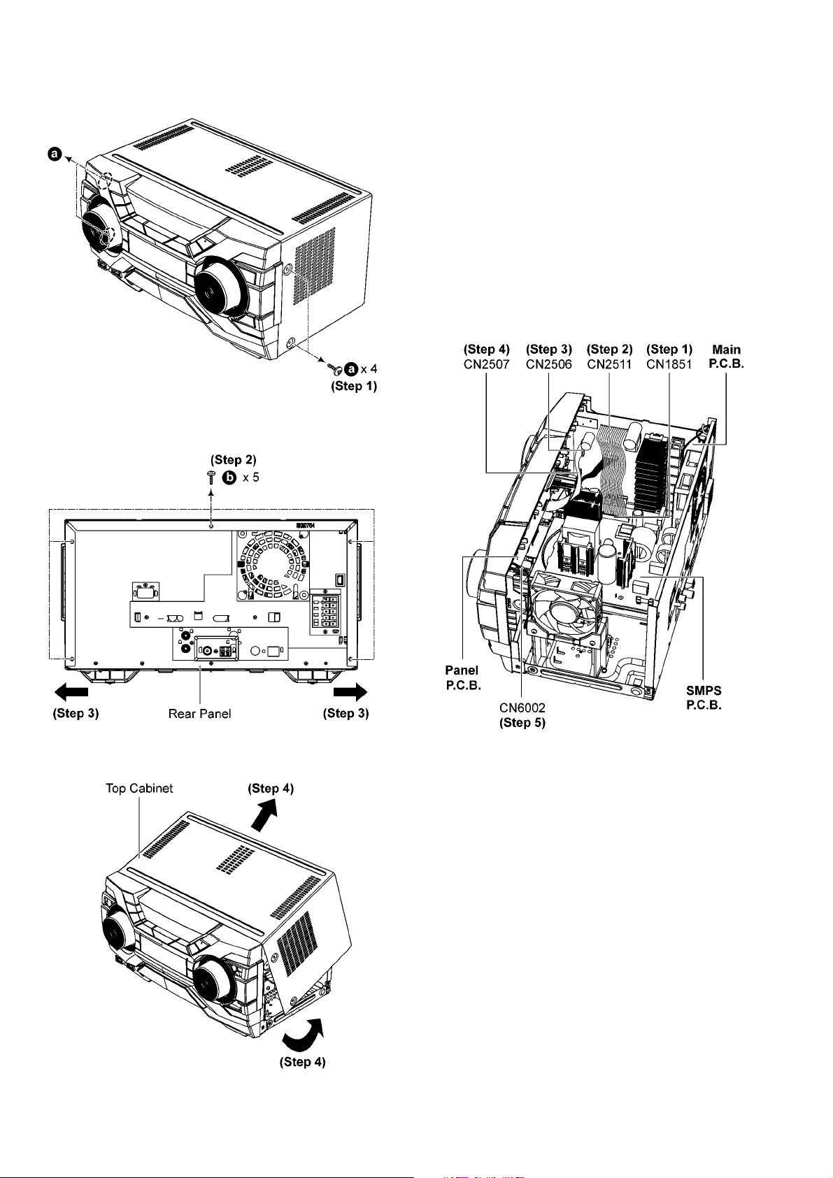
8.4. Disassembly of Top Cabinet
Step 1 Remove 4 screws.
Step 2 Remove 5 screws.
Step 3 Slightly release both sides of Top Cabinet.
8.5. Disassembly of Front Panel Unit
• Refer to “Disassembly of Top Cabinet”.
Step 1 Detach 13P Cable at connector (CN1851) on SMPS
P.C.B..
Step 2 Detach 9P Cable at connector (CN2511) on Main
P.C.B..
Step 3 Detach 22P FFC at connector (CN2506) on Main
P.C.B..
Step 4 Detach 4P Cable at connector (CN2507) on Main
P.C.B..
Step 5 Detach 2P Cable at connector (CN6002) on Panel
P.C.B..
Step 4 Slightly lift up to remove Top Cabinet.
24
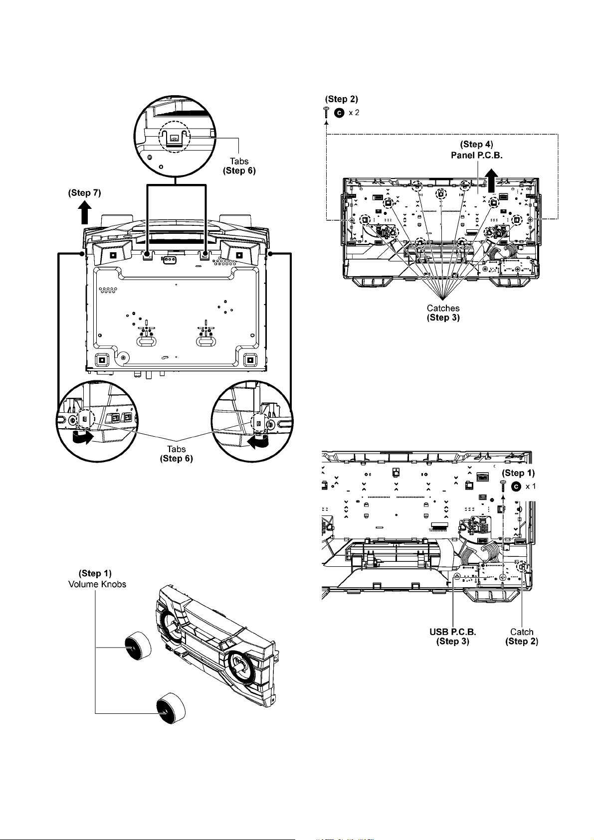
Step 6 Release tabs on both sides of Front Panel Unit and at
bottom of unit.
Step 7 Detach to remove Front Panel Unit.
Step 2 Remove 2 screws.
Step 3 Release catches.
Step 4 Lift up to remove Panel P.C.B..
8.6. Disassembly of Panel P.C.B.
• Refer to “Disassembly of Top Cabinet”.
• Refer to “Disassembly of Front Panel Unit”.
Step 1 Remove Volume Knobs.
8.7. Disassembly of USB P.C.B.
• Refer to “Disassembly of Top Cabinet”.
• Refer to “Disassembly of Front Panel Unit”.
Step 1 Remove screw.
Step 2 Release catch.
Step 3 Lift up to remove USB P.C.B..
25
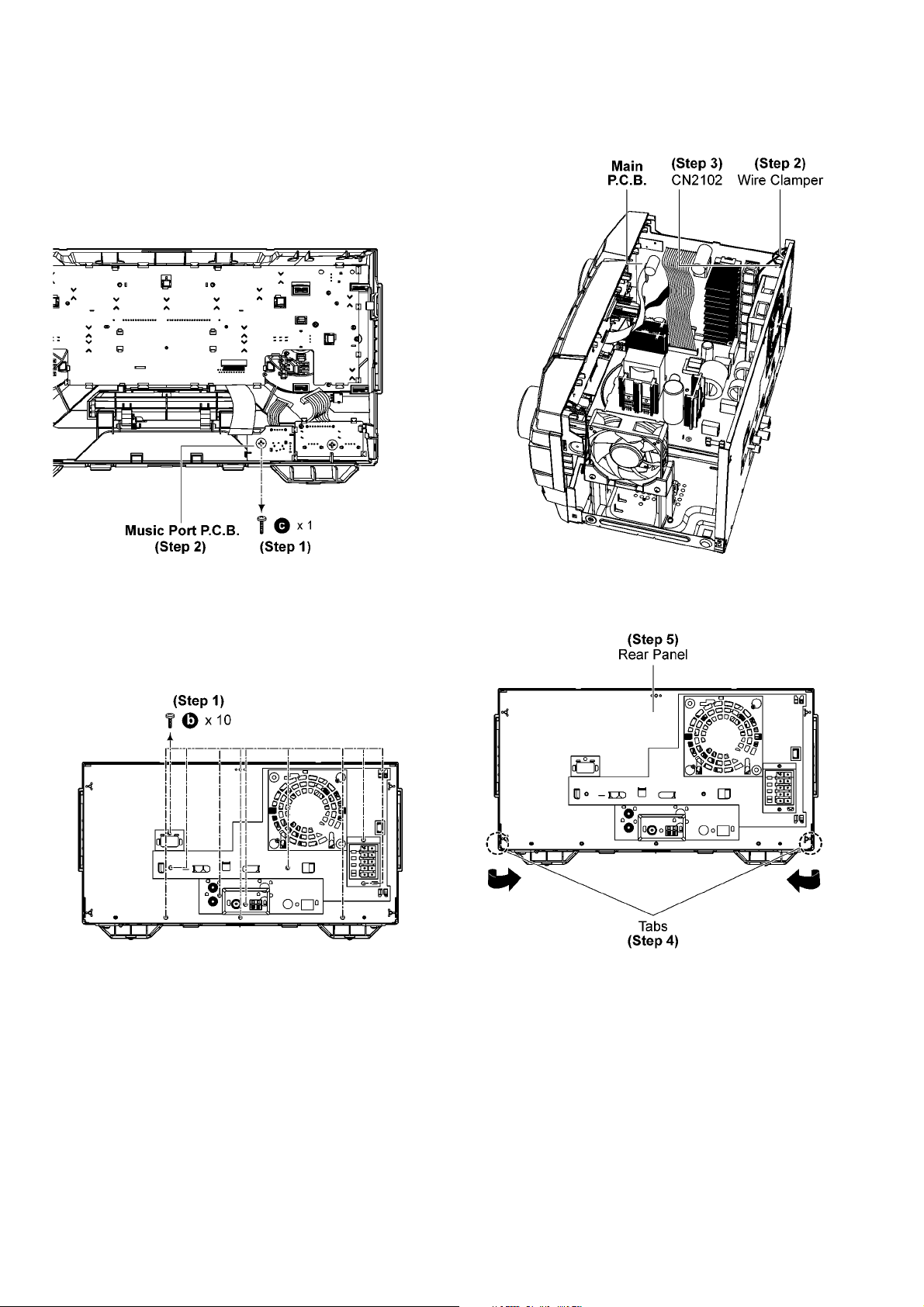
8.8. Disassembly of Music Port P.C.B.
• Refer to “Disassembly of Top Cabinet”.
• Refer to “Disassembly of Front Panel Unit”.
Step 1 Remove screw.
Step 2 Lift up to remove Music Port P.C.B..
Step 2 Lift up Wire Clamper.
Step 3 Detach 2P Cable at connector (CN2102) on Main
P.C.B..
8.9. Disassembly of Rear Panel
• Refer to “Disassembly of Top Cabinet”.
Step 1 Remove 10 screws.
Step 4 Release tabs.
Step 5 Remove Rear Panel.
26
 Loading...