

Panasonic SAAKX-30-PH, SAAKX-30-PN Service manual
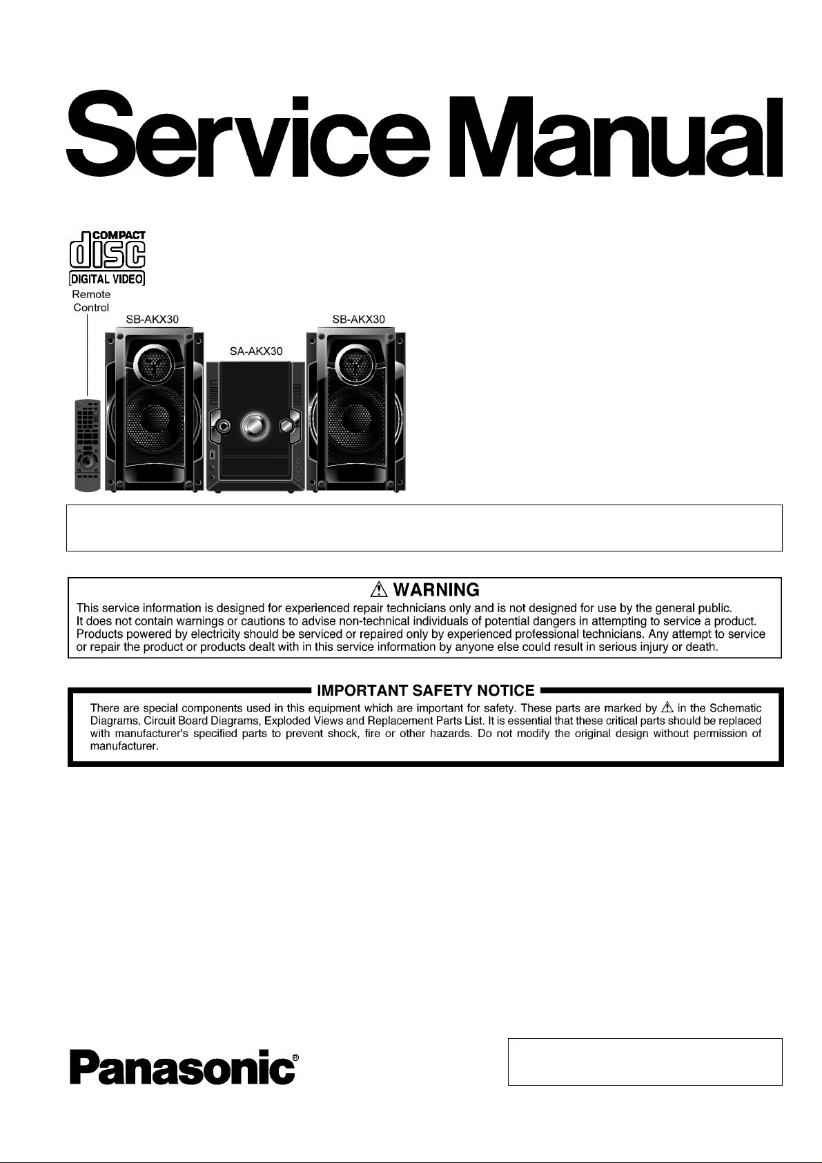
PSG1002032CE
CD Stereo System
Model No. SA-AKX30PH
SA-AKX30PN
Product Color: (K)...Black Type
Notes: This model’s CD Mechanism Unit is DLS6C. Please refer to the original service manual
(Order No. MD0803034CE) for this mechanism
TABLE OF CONTENTS
PAGE PAGE
1 Safety Precautions----------------------------------------------- 3
1.1. General Guidelines---------------------------------------- 3
1.2. Before Use (For PH only)-------------------------------- 3
1.3. Caution For Fuse Replacement ------------------------ 3
1.4. Before Repair and Adjustment ------------------------- 4
1.5. Protection Circuitry---------------------------------------- 4
1.6. Safety Parts Information --------------------------------- 4
2 Warning-------------------------------------------------------------- 6
2.1. Prevention of Electrostatic Discharge (ESD)
to Electrostatic Sensitive (ES) Devices -------------- 6
2.2. Precaution of Laser Diode------------------------------- 7
2.3. Service caution based on Legal restrictions--------8
2.4. Handling Precautions for Traverse Unit--------------9
3 Se rvice Navigation --------------------------------------------- 11
3.1. Service Information-------------------------------------- 11
4 Specifications ----------------------------------------------------12
5 Location of Controls and Components------------------ 13
5.1. Main Unit Key Button Operation----------------------13
5.2. Remote Control Key Button Operation ------------- 14
5.3. Media Information---------------------------------------- 15
6 Self-Diagnostic and Special Mode Setting -------------16
6.1. Cold-Start --------------------------------------------------16
6.2. Doctor Mode Table--------------------------------------- 17
© Panasonic Corporation 2010. All rights reserved.
Unauthorized copying and distribution is a violation
of law.

6.3. Reliability Test Mode (CD Mechanism Unit
(DLS6C)) ---------------------------------------------------19
6.4. Self-Diagnostic Mode -----------------------------------20
6.5. Self-Diagnostic Error Code Table--------------------21
7 Troubleshooting Guide----------------------------------------22
7.1. Troubleshooting Guide for F61 and/or F76--------22
7.2. Part Location ----------------------------------------------23
7.3. D-Amp IC Operation & Contro l -----------------------26
8 Service Fixture & Tools---------------------------------------28
8.1. Service Tools and Equipment-------------------------28
9 Disassembly and Assembly Instructions---------------29
9.1. Disassembly Flow Chart--------------------------------30
9.2. Main Components and P.C.B. Locations-----------31
9.3. Disassembly of Top Cabinet---------------------------32
9.4. Disassembly of Tuner P.C.B.--------------------------32
9.5. Disassembly of Front Panel Assembly -------------33
9.6. Disassembly of Panel P.C.B.--------------------------34
9.7. Disassembly of Remote Sensor P.C.B.-------------36
9.8. Disassembly of CD Open Button P.C.B.------------36
9.9. Disassembly of Jupiter P.C.B.-------------------------37
9.10. Disassembly of Music Port/Headphone P.C.B.---37
9.1 1 . Disassembly of CD Lid----------------------------------38
9.12. Disassembly of Main P.C.B. ---------------------------39
9.13. Replacement of Regulator IC (IC2010)-------------40
9.14. Disassembly of D-Amp P.C.B.------------------------41
9.15. Replacement of Audio Digital Amp IC
(IC5900) ----------------------------------------------------42
9.16. Disassembly of SMPS P.C.B.-------------------------44
9.17. Replacement of Switching Regulator IC
(IC5701) ----------------------------------------------------45
9.18. Replacement of Rectifier Diode (D5702)-----------47
9.19. Replacement of Regulator Diode (D5801)---------48
9.20. Replacement of Regulator Diode (D5802)---------49
9.21. Replacement of Regulator Diode (D5803)---------50
9.22. Disassembly of CD Mechanism Unit (DLS6C) ---51
9.23. Disassembly of Rear Panel----------------------------53
9.24. Disassembly of Voltage Selector P.C.B. (For
PH only) ----------------------------------------------------54
9.25. Disassembly of CD Servo P.C.B.---------------------55
10 Replacement of Traverse Unit------------------------------56
10.1. Disassembling Procedures----------------------------56
10.2. Assembling Procedure----------------------------------57
11 Service Position -------------------------------------------------59
11.1. Checking and Repairing of Main P.C.B. ------------59
11.2. Checking and Repairing of D-Amp P.C.B. ---------59
11.3. Checking and Repairing of Panel P.C.B.-----------59
11.4. Checking and Repairing of Jupiter P.C.B.----------59
11.5. Checking and Repairing of SMPS P.C.B. ----------60
12 Voltage & Waveform Chart-----------------------------------61
12.1. CD SERVO P.C.B. ---------------------------------------61
12.2. Main P.C.B. (1/2)-----------------------------------------62
12.3. Main P.C.B. (2/2)-----------------------------------------63
12.4. Jupiter P.C.B. (1/3)---------------------------------------64
12.5. Jupiter P.C.B. (2/3)---------------------------------------65
12.6. Jupiter P.C.B. (3/3)---------------------------------------66
12.7. Panel P.C.B.-----------------------------------------------66
12.8. D-Amp P.C.B. ---------------------------------------------66
12.9. SMPS P.C.B.----------------------------------------------67
12.10. Tuner P.C.B. -----------------------------------------------67
12.11. Waveform Table (1/2) -----------------------------------68
13 Illustration of ICs, Transistor and Diode ----------------69
14 Simplified Block Diagram------------------------------------ 71
14.1. Overall Simplified Block Diagram-------------------- 71
14.2. D-Amp Block Diagram---------------------------------- 72
15 Block Diagram--------------------------------------------------- 73
15.1. Servo/System Control ---------------------------------- 73
15.2. I C Terminal Chart (Servo/System Control)-------- 74
15.3. Audio-------------------------------------------------------- 75
15.4. Power Amplifier ------------------------------------------ 76
15.5. Power Supply--------------------------------------------- 77
16 Wiring Connection Diagram -------------------------------- 78
17 Schematic Diagram Notes----------------------------------- 79
18 Schematic Diagram-------------------------------------------- 81
18.1. CD Servo Circuit ----------------------------------------- 81
18.2. Main Circuit------------------------------------------------ 82
18.3. Jupiter Circuit --------------------------------------------- 88
18.4. Panel Circuit ---------------------------------------------- 92
18.5. CD Open Button, Remote Sensor, Tuner,
Music Port/Headphone Circuit------------------------ 94
18.6. D-Amp Circuit--------------------------------------------- 95
18.7. SMPS Circuit---------------------------------------------- 96
18.8. Voltage Selector Circuit (For PH Only)------------- 98
19 Printed Circuit Board------------------------------------------ 99
19.1. CD Servo & Voltage Selector P.C.B.---------------- 99
19.2. Main P.C.B.-----------------------------------------------100
19.3. Jupiter P.C.B.--------------------------------------------101
19.4. Panel P.C.B.----------------------------------------------102
19.5. CD Open Button, Remote Sensor, Tuner,
Music Port/Headphone & D-Amp P.C.B.----------103
19.6. SMPS P.C.B. (For PH Only) -------------------------104
19.7. SMPS P.C.B. (For PN Only) -------------------------105
20 Terminal Function of ICs------------------------------------107
20.1. IC2003 (RFKWAKX30PN): IC MICROPROCESSOR -------------------------------------------107
20.2. IC6901(C0HBB0000057): IC FL Driver-----------108
21 Exploded View and Replacement Parts List----------109
21.1. Exploded View and Mechanical replacement
Part List ---------------------------------------------------109
21.2. Electrical Replacement Part List--------------------115
2
1 Safety Precautions
1.1. General Guidelines
1. Wh en servicing, observe the original lead dress. If a short circuit is found, replace all parts which have been overheated or
damaged by the short circuit.
2. After servicing, see to it that all the protective devices such as insulation barriers, insulation papers shields are properly
installed.
3. After servicing, carry out the following leakage current checks to prevent the customer from being exposed to shock hazards.
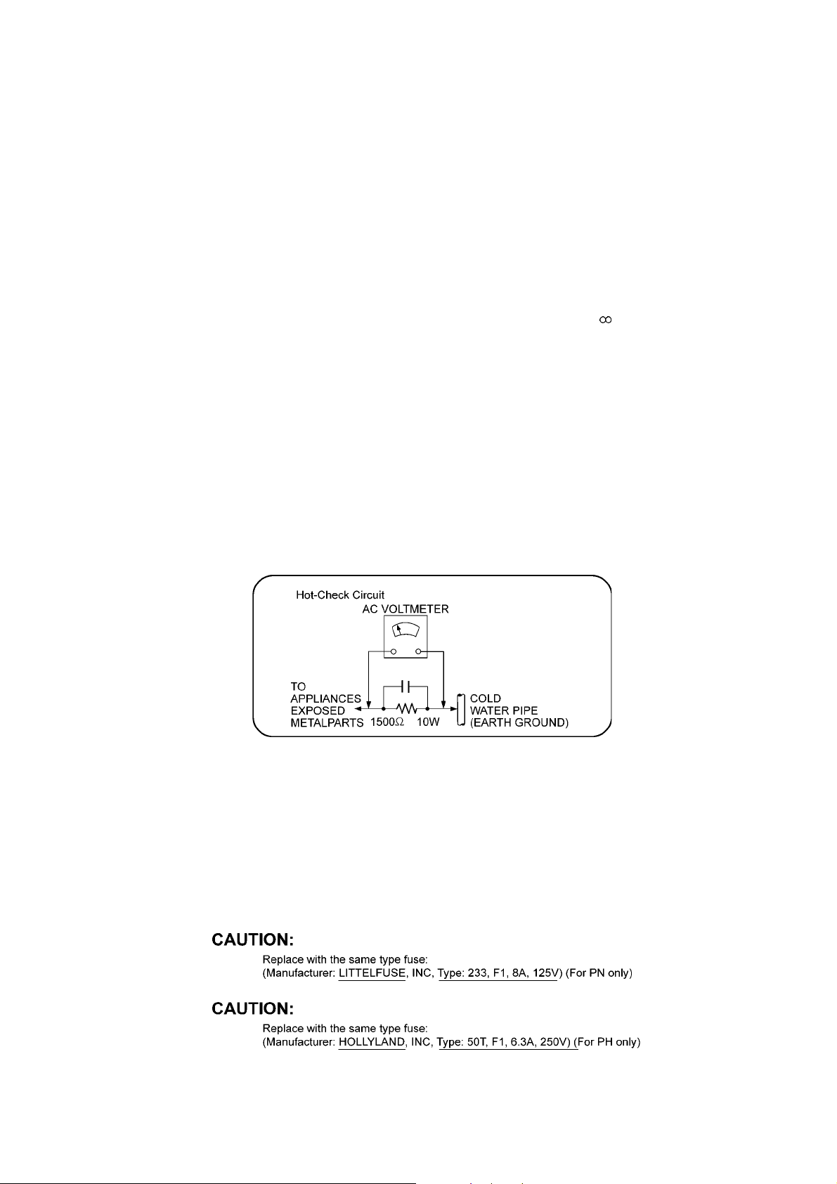
1.1.1. LEAKAGE CURRENT COLD CHECK
1. Unplug the AC cord and connect a jumper between the two prongs on the plug.
2. Measure the resistance value, with an o hmmeter, between the jumpered AC plug and each exposed metallic cabinet part on
the equipment such as screwheads, connectors, control shafts, etc. When the exposed metallic part has a return path to th e
chassis, the reading should be between 1MΩ and 5.2MΩ.
When the exposed metal does not have a return path to the chassis, the reading must be
1.1.2. LEAKAGE CURRENT HOT CHECK
1. Plug the AC cord directly into the AC outlet. Do not use an isolation transformer for this check.
2. Connect a 1.5kΩ, 10 watts resistor, in parallel with a 0.15µF capacitors, between each exposed metallic part on the set and a
good earth ground such as a water pipe, as shown in Figure 1.
3. Use an AC voltmeter, with 1000 ohms/volt or more sensitivity, to measure the potential across the resistor.
4. Check each exposed metallic part, and measure the voltage at each point.
5. Reverse the AC plug in the AC outlet and repeat each of the above measurements.
6. Th e potential at any point should not exceed 0.75 volts RMS. A leakage current tester (Simpson Model 229 or equivalent)
may be used to make the hot checks, leakage current must not exceed 1/2 milliamp. In case a measurement is outside of the
limits specified, there is a possibility of a shock hazard, and the equipment should be repaired and rechecked before it is
returned to the customer.
Figure 1
1.2. Before Use (For PH only)
Be sure to disconnect the mains cord before adjusting the voltage selector.
Use a minus(-) screwdriver to set the voltage selector (on the rear panel) to the voltage setting for the area in which the unit will be
used. (If the power supply in your area is 110V ~ 127V or 220V ~ 240V, set to the “110V ~ 127V or 220V ~ 240V” position.)
Note that this unit will be seriously damaged if this setti ng is not made correctly. (There is no voltage selector for some countries,
the correct voltage is already set.)
1.3. Caution For Fuse Replacement
3
1.4. Before Repair and Adjustment
Disconnect AC power to discharge unit AC Capacitors as such (C5701, C5703, C5704, C5705, C5706, C5707, C570 8) through a
10 Ω, 10 W resistor to ground.
Caution:
DO NOT SHORT-CIRCUIT DIRECTLY (with a screwdriver blade, for instance), as this may destroy solid state devices.
After repairs are completed, restore power gradually using a variac, to avoid overcurrent.
Current consumption at AC 120 V, 60 Hz in NO SIGNAL mode volume mi nimal should be ~ 500 mA. (PN)
Current consumption at AC 110~127 V / 220~240 V, 50/60 Hz in NO SIGNAL mode volume minimal should be ~ 500 mA. (PH)
1.5. Protection Circuitry
The protection circuitry may have operated if either of the following conditions are noticed:
• No sound is heard when the power is turned on.
• Sound stops during a performance.
The function of this circuitry is to prevent circuitry damage if, for example, the positive and negative speaker connection wires are
“shorted”, or if speaker systems with an impedance less than the indicated rated impedance of the amplifier are used.
If this occurs, follow the procedure outlines below:
1. Turn off the power.
2. Determine the cause of the problem and correct it.
3. Turn on the power once again after one minute.
Note:
When the protection circuitry functions, the unit will not operate unless the power is first turned off and then on again.
1.6. Safety Parts Information
Safety Parts List:
There are special components used in this equipment which are important for safety.
These parts are marked by in the Schematic Diagrams & Replacement Parts List. It is essential that these critical parts
should be replaced with manufacturer’s specified parts to prevent shock, fire or other hazards. Do not modify the original design
without permission of manufacturer.
Safety Ref. No. Part No. Part Name & Description Remarks
6 REXX1030 1P RED WIRE (VOLTAGE-SMPS) PH
7 REXX1031 1P BLACK WIRE (VOLTAGE-SMPS) PH
13 RGRX1002C-A3 REAR PANEL PN
13 RGRX1002D-A2 REAR PANEL PH
37 RKMX1003-K TOP CABINET
401 RAEX0190Z-V TRAVERSE UNIT
A2 K2CB2CB00021 AC CORD PN
A2 K2CQ2CA00007 AC CORD PH
A3 K2DAYYY00002 AC CORD PH
A3 RQTX1090-M O/I BOOK (Sp) PN
A3 RQTX1091-M O/I BOOK (Sp) PH
A3 RQTX1100-M O/I BOOK (En) PN
PCB3 REPX0809A SMPS P.C.B. (RTL) PN
PCB3 REPX0809C SMPS P.C.B. (RTL) PH
PCB10 REPX0809C VOLTAGE SELECTOR P.C.B. (RTL) PH
DZ5701 ERZV10V511CS ZNR
S5701 K0ABCA000007 SW VOLTAGE SELECTOR PH
L5703 G0B612H00002 LINE FILTER
T5701 ETS39AG4M6AD MAIN TRANSFORMER PH
T5701 ETS39AG4NGAD MAIN TRANSFORMER PN
T5751 ETS19AB2E6AG SUB TRANSFORMER
T6000 G4DYA0000214 SWITCHING TRANS
PC5701 B3PBA0000402 PHOTO COUPLER
PC5702 B3PBA0000402 PHOTO COUPLER
PC5720 B3PBA0000402 PHOTO COUPLER
PC5799 B3PBA0000402 PHOTO COUPLER
F1 K5D632BK0007 FUSE PH
F1 K5D802APA008 FUSE PN
TH5702 D4CAA2R20001 THERMISTOR
TH5860 D4CC11040013 THERMISTOR
TH5900 D4CC11040013 THERMISTOR
P5701 K2AA2B000011 AC INLET PH
P5701 K2AB2B000007 AC INLET PN
C2253 F1H1H470A004 47pF 50V
4

Safety Ref. No. Part No. Part Name & Description Remarks
C2254 F1H1H470A004 47pF 50V
C2263 F2A0J471A016 470uF 6.3V
C5701 F0CAF334A105 0.33uF
C5703 F0CAF104A105 0.1uF PH
C5703 F0CAF224A105 0.22uF PN
C5704 F1BAF1020020 1000pF
C5705 F1BAF1020020 1000pF
C5706 F1BAF1020020 1000pF PH
C5707 F1BAF1020020 1000pF PH
C5708 F1BAF1020020 1000pF
5

2Warning
2.1. Prevention of Electrostatic Discharge (ESD) to Electrostatic Sensitive
(ES) Devices
Some semiconductor (solid state) devices can be damaged easily by static electricity. Such components commonly are called Electrostatically Sensitive (ES) Devices. Examples of typical ES devices are integrated circuits and some field-effect transistors and
semiconductor "chip" components. The following techniques should be used to help reduce the incidence of component da mage
caused by electrostatic discharge (ESD).
1. Immediately before handling any semiconductor component or semiconductor-equipped assembly, drain off any ESD on your
body by touching a known earth ground. Alternatively, obtain and wear a commercially available discharging ESD wrist strap,
which should be removed for potential shock reasons prior to applying power to the unit under test.
2. After removing an electrical assembly equipped with ES devices, p lace the assembly on a cond ucti ve surface su ch as a luminum foil, to prevent electrostatic charge buildup or exposure of the assembly.
3. Use only a grounded-tip soldering iron to solder or unsolder ES devices.
4. Use only an anti-static solder removal device. Some solder removal devices not classified as “anti-static (ESD protected)” can
generate electrical charge sufficient to damage ES devices.
5. Do not use freon-propelled chemicals. These can generate electrical charges sufficient to damage ES devices.
6. Do not remove a replacement ES device from its protective package until immediately before you are ready to install it. (Most
replacement ES devices are packaged with leads electrically shorted together by conductive foam, aluminum foil or comparable conductive material).
7. Immediately before removing the protective material from the leads of a replacement ES device, touch the protective material
to the chassis or circuit assembly into which the device will be installed.
Caution:
Be sure no power is applied to the chassis or circuit, and observe all other safety precautions.
8. Minimize bodily motions when handling unpackaged replacement ES devices. (Otherwise harmless motion such as the
brushing together of your clothes fabric or the lif ting of your foot from a carpeted floor can generate static electricity (ESD) suf-
ficient to damage an ES device).
6
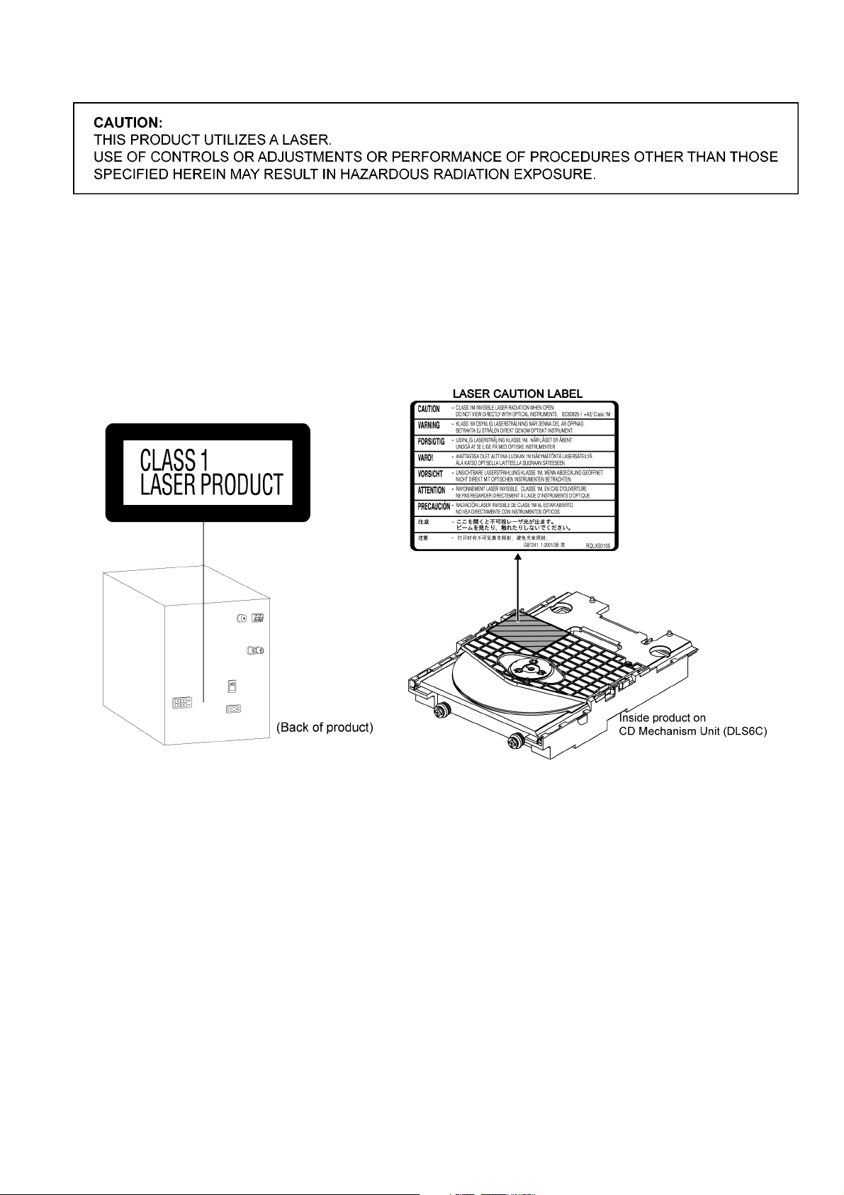
2.2. Precaution of Laser Diode
Caution:
This product utilizes a laser diode with the unit turned “on”, invisible laser radiation is emitted from the pickup lens.
Wavelength: 785 nm (CD)
Maximum output radiation power from pickup: 100 µW/VDE
Laser radiation from the pickup unit is safety level, but be sure the followings:
1. Do not disassemble the pickup unit, since radiation from exposed laser diode is dangerous.
2. Do not adjust the variable resistor on the pickup unit. It was already adjusted.
3. Do not look at the focus lens using optical instruments.
4. Recommend not to look at pickup lens for a long time.
7

2.3. Service caution based on Legal restrictions
2.3.1. General description about Lead Free Solder (PbF)
The lead free solder has been used in the mounting process of all electrical compone nts on the printed circuit boards used for this
equipment in considering the globally environmental conservation.
The normal solder is the alloy of tin (Sn) and lead (Pb). On the other hand, the lead free solder is the alloy mainl y consists of tin
(Sn), silver (Ag) and Copper (Cu), and the melting point of the lead free solder is higher approx.30 degrees C (86°F) more than that
of the normal solder.
Definition of PCB Lead Free Solder being used
The letter of “PbF” is printed either foil side or components side on the PCB using the lead free solder.
(See right figure)
Service caution for repair work using Lead Free Solder (PbF)
• The lead free solder has to be used when repairing the equipment for which the lead free solder is used.
(Definition: The letter of “PbF” is printed on the PCB using the lead free solder.)
• To put lead free solder, it should be well molten and mixed with the original lead free solder.
• Remove the remaining lead free solder on the PCB cleanly for soldering of the new IC.
• Since the melting point of the lead free solder is higher than that of the normal lead solder, it takes the longer time to melt the
lead free solder.
• Use the soldering iron (more than 70W) equi pped with the temperature co ntrol after setting the temp erature at 350±30 degrees
C (662±86°F).
Recommended Lead Free Solder (Service Parts Route.)
• The following 3 types of lead free solder are available through the service parts route.
RFKZ03D01K-----------(0.3mm 100g Reel)
RFKZ06D01K-----------(0.6mm 100g Reel)
RFKZ10D01K-----------(1.0mm 100g Reel)
Note
* Ingredient: tin (Sn), 96.5%, silver (Ag) 3.0%, Copper (Cu) 0.5%, Cobalt (Co) / Germanium (Ge) 0.1 to 0.3%
8
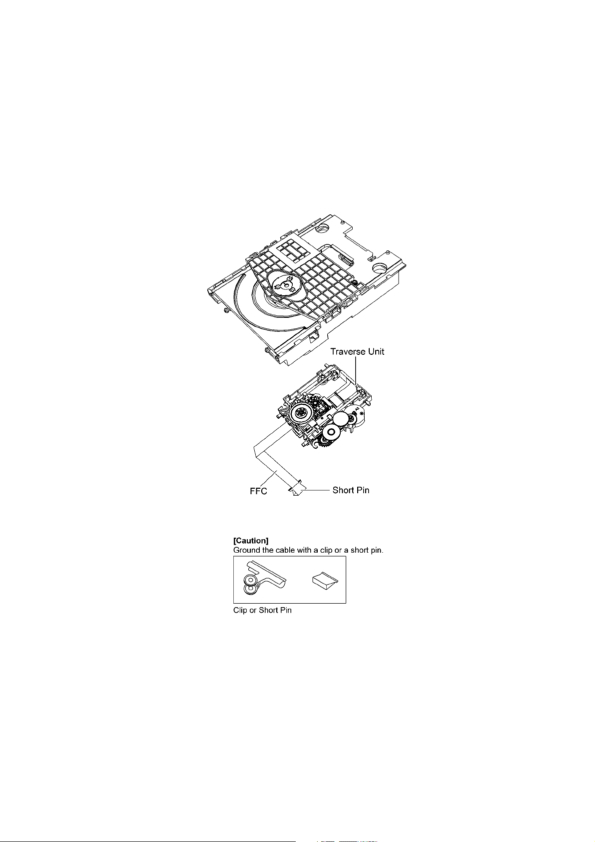
2.4. Handling Precautions for Traverse Unit
The laser diode in the optical pickup unit may break down due to static electricity of clothes or human b ody. Special care must be
taken avoid caution to electrostatic breakdown when servicing and handling the laser diode in the traverse unit.
2.4.1. Cautions to Be Taken in Handling the Optical Pickup Unit
The laser diode in the optical pickup un it may be damaged due to electrostatic discharge generating from clothes or human body.
Special care must be taken avoid caution to electrostatic discharge damage when servicing the laser diode.
1. Do not give a considerable shock to the optical pickup unit as it has an extremely high-precise structure.
2. To prevent the laser diode from the electrostatic discharge damage, the flexible cable of the optical pickup unit removed
should be short-circuited with a short pin or a clip.
3. The flexible cable may be cut off if an excessive force is applied to it. Use caution when handling the flexible cable.
4. The antistatic FPC is connected to the new optical pickup unit. After replacing the optical pickup unit and connecting the flexible cable, cut off the antistatic FPC.
2.4.2. Grounding for electrostatic breakdown prevention
Some devices such as the DVD player use the optical pickup (laser diode) and the optical pickup will be damaged by static electricity in the working environment. Proceed servicing works under the working environment where grounding works is completed.
2.4.2.1. Worktable grounding
1. Put a conductive material (sheet) or iron sheet on the area where the optical pickup is placed, and ground the sheet.
9
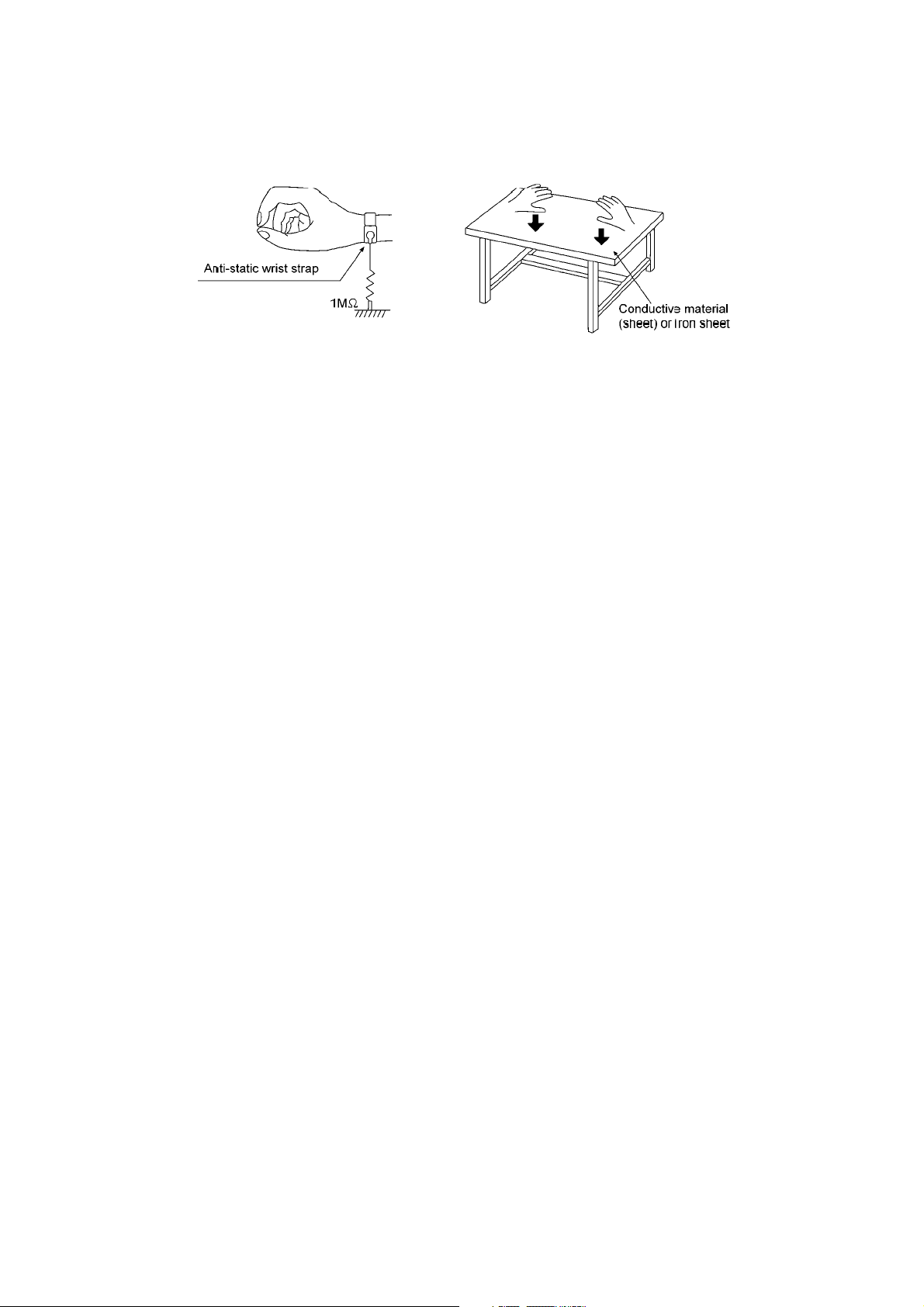
2.4.2.2. Human body grounding
1. Use the anti-static wrist strap to discharge the static electricity form your body.
10

3 Service Navigation
3.1. Service Information
This service manual contains technical information which will allow service personnel’s to understand and service this model.
Please place orders using the parts list and not the drawing reference numbers.
If the circuit is changed or modified, this information wil l be fol lowed by supplemen t service manual to be filed with original se rvice
manual.
• CD Mechanism unit (DLS6C):
1) This model uses CD Mechanism Unit (DLS6C).
2) This service manual does not contain the following information on CD Mechanism Unit (DLS6C)
- Schematic Diagram, Block Diagram and P.C.B. layout of CD Mechanism Unit (DLS6C) P.C.B.
- Parts List for individual parts of CD Mechanism Unit (DLS6C).
- Exploded View and Part List for individual parts of CD Mechanism Unit (DLS6C).
Please refer to original service manual (Order No. MD0803034CE)
• Micro-processo:
1) The following components are supplied as an assembled part.
- Micro-processor IC, IC2300 (RFKWMAKX30PN)
• Speaker system :
1) This model uses speakers, SB-AKX30PN-K (PSG1002019CE)
11

4 Specifications
Q AMPLIFIER SECTION
RMS output power stereo mode
Front Ch (both channels driven)
160 W per channel (3 Ω), 1 kHz, 10% THD
Total RMS stereo mode power
350 W
PMPO output power
3500 W
Q FM/AM TUNER, TERMINALS SECTION
Preset station FM 30 stations
AM 15 stations
Frequency Modulation (FM)
Frequency range
For PH only
87.50 to 108.00 MHz (50 kHz step)
For PN only
87.9 to 107.9 MHz (200 kHz step)
87.5 to 108.0 MHz (100 kHz step)
Antenna terminal (s)
75 Ω (unbalanced)
Amplitude Modulation (AM)
Frequency range
For PH only
522 to 1629 kHz (9 kHz step)
520 to 1630 kHz (10 kHz step)
For PN only
520 to 1710 kHz (10 kHz step)
AUX Input
RCA pin jack
Headphone jack
Terminal Stereo,3.5 mm jack
Output level (CD,1 KHz, -20dB) 32 Ω(Max)
Music port (front)
Sensitivity 100 mV,4.7k Ω
Terminal Stereo.3.5 mm jack
Q DISC SECTION
Discs played (8 cm or 12 cm)
(1) CD-Audio (CD-DA)
(2) CD-R/RW (CD-DA, MP3* formatted disc)
(3) MP3*
*MPEG-1 layer 3,MPEG-2 Layer 3
Pick up
Wavelength 795 nm(CD)
Laser Power CLASS 1 (CD)
Audio output (Disc)
Number of channels 2 (FL, FR)
FL = Front left channel
FR = Front right channel
Q USB SECTION
USB Port
USB standard USB 2.0 full speed
Media file format support MP3 (*.mp3)
USB device file system FAT12, FAT16, FAT32
USB Port power 500 mA (max)
Bit Rate 16kbps to 320 kbps (playback)
USB recording
Bit Rate 128 kbps / 192kbps / 320kbps
USB recording speed 1x,4x (CD only)
recording file format MP3 (*.mp3)
Memory section
Memory
Memory size 2 GB
Memory File format MP3 (*.mp3)
Memory recording
Bit Rate 128 kbps / 192 kbps / 320kbps
Memory Recording speed 1x,4x, (CD only)
Recording file format MP3 (*.mp3)
Capacity of total song recoreded 510 song
(Use 128 kbps, approximately 1 song + 4 mins)
Q GENERAL
Power supply
For PH only
AC 110 to 127 V, 50 Hz
AC 220 to 240 V, 60 Hz
For PN only
AC 120 V, 60 Hz
Power Consumption
For PH only
72 W
For PN only
68 W
Dimensions (W x H x D) 250 mm x 336 mm x 245 mm
Mass 3.2 kg
Operating temperature range 0 °C to +40 °C
Operating humidity range 35% to 80% RH
(no condensation)
Power Consumption in st andby
mode
For PH only 0.3 W (Approximate)
For PN only 0.2 W (Approximate)
Notes
1. Specifications are subject to change without notice.
Mass and dimensions are approximate.
2. Total harmonic distortion is measured by the digital spectrum
analyzer.
Q System: SC-AKX30PN-K
Main Unit: SA-AKX30PN-K
Front Speakers: SB-AKX30PN-K
Q System: SC-AKX30PH-K
Main Unit: SA-AKX30PH-K
Front Speakers: SB-AKX30PN-K
12
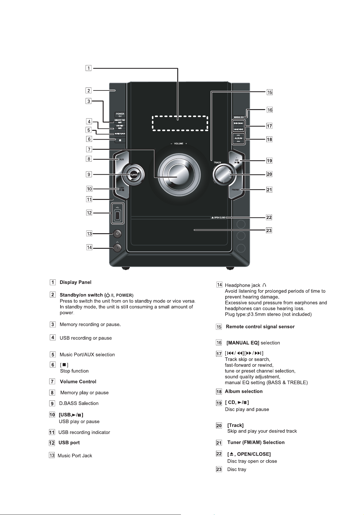
5 Location of Controls and Components
5.1. Main Unit Key Button Operation
13
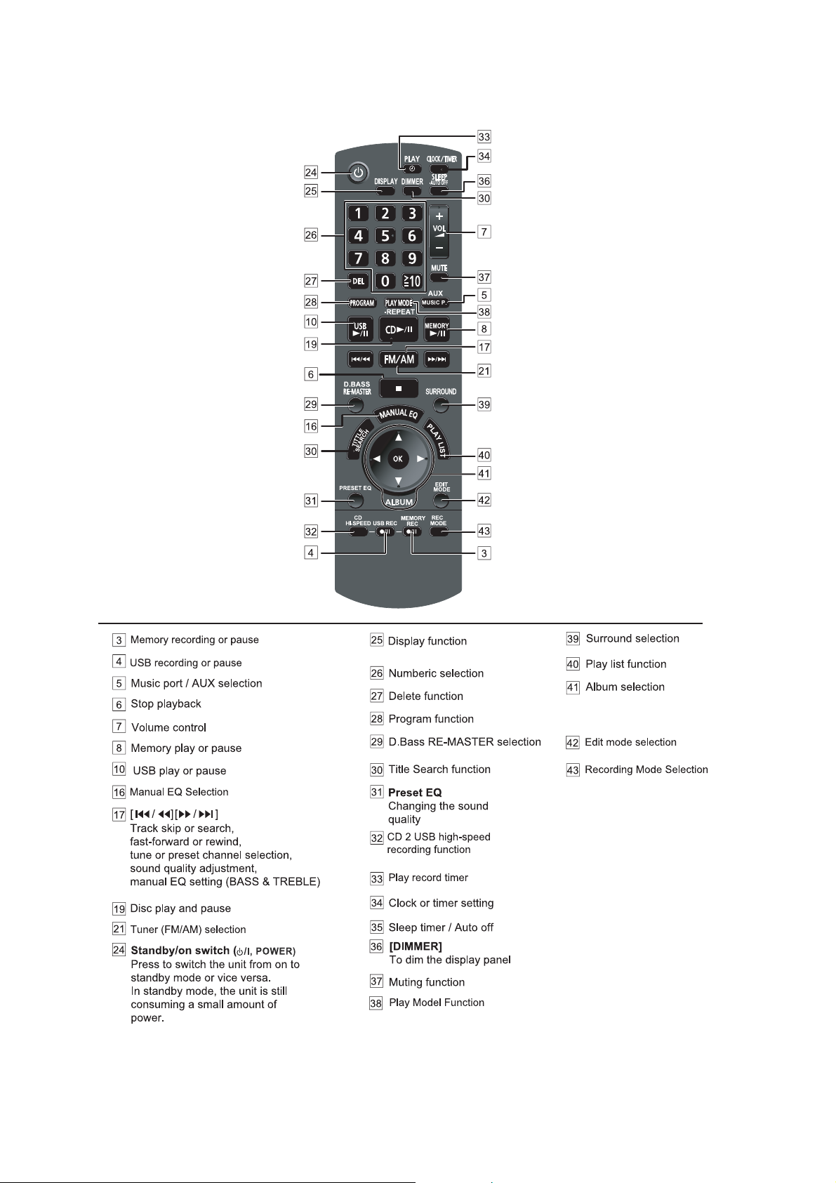
5.2. Remote Control Key Button Operation
14
5.3. Media Information
15

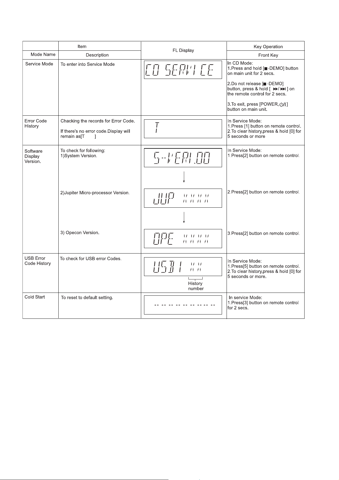
6 Self-Diagnostic and Special Mode Setting
6.1. Cold-Start
Here is the procedure to carry out cold-start or initialize to shipping mode.
1. Unplug AC power cord
2. Press & hold [POWER] button
3. Plug AC power cord while [POWER] button being pressed
FL Display will show “_ _ _ _ _ _ _ _”
4. Release [POWER] button
16
6.2. Doctor Mode Table
6.2.1. Doctor Mode Table 1
Doctor Mode
Micro-P Version
Display
Item
DescriptionMode Name
To enter into Doctor Mode
To check the firmware version
for Jupiter & Microprocessor IC.
Display 1 will display for 2 secs,
followed by display 2.
Display 1:
Display 2:
FL Display
Key Operation
Front Key
1.In CD Mode:
Press [ ] button on main
unit follow by [4] and [7] on
remote control.
2.To exit, press [OK] button on
remote control or press
[POWER, /I] button on main
unit or remote control.
In Doctor Mode:
1.Press [2] button on
remote control.
Jupiter
Micro-P
Version
Micro-processor
Version
17
6.2.2. Doctor Mode Table 2
Cold Start
Volume Setting
Check
FL Display
Check
CD Open
Check
Item
DescriptionMode Name
To active cold start upon next AC
power up when reset start is execute
the next time.
To check the volume setting of a main
unit.
To check the FL segment display
All segment will light up while all LED
blink at 0.5s,intervals.(if any)
To excute CD OPEN operation.
FL Display
Press [7]: VOLUME50
Press [8]: VOLUME35
Press [9]: VOLUME0
Press [PLAY MODE]: VOLUME30
Key Operation
Front Key
In Doctor Mode:
1. Press [DISPLAY] button
on remote control.
In Doctor Mode:
1. Press [7],[8],[9],
[PLAY MODE] button on
remote control.
Volume
In Doctor mode:
1. Press [1] button on
remote control.
In Doctor mode:
1. Press [DEL] button on
remote control.
DLS6 Reliability
Test (Loading)
To determine DLS6
Open/Close operation.
In this mode, the tray will open &
close.
Note: Refer to Section 6.3 Fig 1 for
process flow.
In Doctor Mode:
1.Press [>10], follow by [1]
and [1] buttons on remote
control.
The counter will
increment by one.
When reach 9999
will change to 0000
18
6.3. Reliability Test Mode (CD Mechanism Unit (DLS6C))
Below is the process flow chart of the aging test for the CD Mechanism Unit (DLS6C).
OPEN
Operation
OPEN wait
fot 1 s
CLOSE
Operation
CLOSE wait
for 5s
Fig. 1. Reliability Test (Loading)
Count up
19
6.4. Self-Diagnostic Mode
20
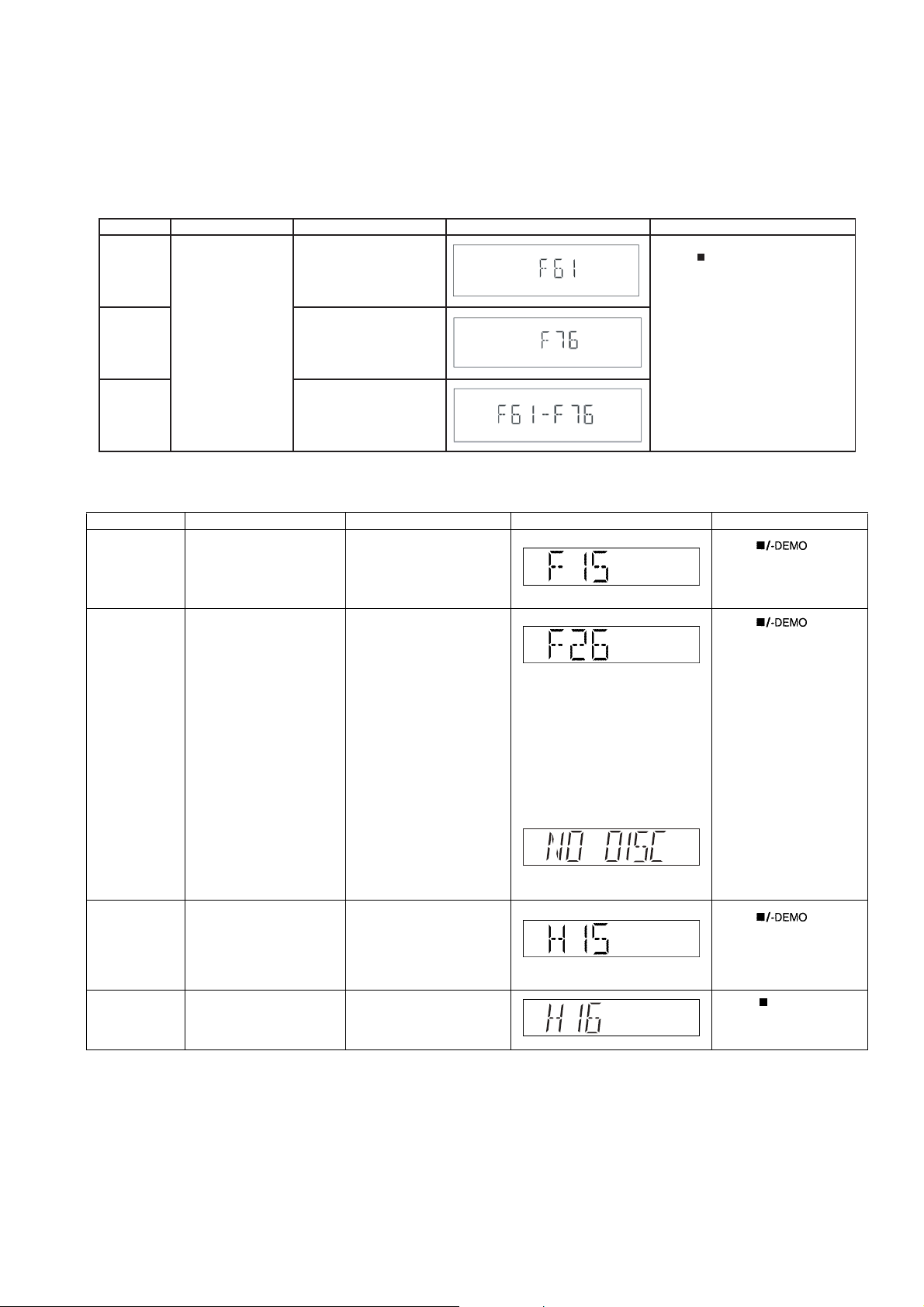
6.5. Self-Diagnostic Error Code Table
Self-Diagnostic Function (Refer Section 6.4. Self-Diagnostic Mode) provides information on any problems occurring for the unit and
its respective components by displaying the error codes. These error code such as U**, H** and F** are stored in memory and held
unless it is cleared.
The error code is automatically display after entering into self-diagnostic mode.
6.5.1. Power Supply Error Code Table
Error Code Diagnosis Contents Description of error Automatic FL Display Remarks
F61 Power Amp IC output
abnormal
F76 DCDET1 = L (NG)
Upon power on,
PCNT=HIGH, DCDET2=L
after checking LSI.
Press [ ] on main unit for
next error.
-DEMO
F61-76 Both DCDET1 and
DCDET2 L(NG)
6.5.2. Mechanism Error Code Table (CD Mechanism Unit (DLS6C))
Error Code Diagnosis Contents Description of error Automatic FL Display Remarks
F15 CD REST SW Abnormal
F26 Communication between
CD servo LSI and micro-p
abnormal.
CD traverse position initial
setting operation fail safe
time is over (10 sec) waiting
for REST SW to turn on.
At the time of switching to
CD function,SENSE = H
shall be detected using
DTMS system setting
command. If the error is
memorized when SENSE
= L is not detected within
fail safe timer time (20ms),
[F26] shall be displayed
simultaneously.This
display shall be retained if
the power is ON and at
CD function. If this error
occurs, CD operation
afterwards shall not be
executed as in the case of
[NO DISC].
Press [ ] on main
unit for next error.
Press [ ] on main
unit for next error.
H15 CD Open SW Abnormal During normal operation
H16
CD closing SW abnormal
CD OPEN SW On fail to be
detected with 3 sec.
During Closing operation,if
"POS_SW_CEN" is not
detected within 3 sec.
21
Press [ ] on main
unit for next error.
Press [ /-DEMO]on main
unit for next error.
7 Troubleshooting Guide
7.1. Troubleshooting Guide for F61 and/or F76
This section illustrates the checking procedures when upon detecting the error of “F61” and/or “F76” after power up of the unit. It is
for purpose of troubleshooting and checking in SMPS, D-Amp & Main P.C.B.
Symptom Remarks
Set cannot ON 1 AC Cord 1 Faulty AC Cord, Loose connection
2 AC Inlet, P5701 2 P5701 solder crack, dry joint.
3 Fuse, F1 3 Fuse, F1 Open
4 Photocoupler 4 PC5702/PC5799 solder crack.
PC5702, PC5799 Dry joint, short circuit, open circuit.
5 Switching IC, IC5701 5 IC5701 Faulty.
6 Switching IC, IC5799 6 IC5799 Faulty.
Set can ON 1 Speaker Output 1 Faulty speaker unit, Loose connection, Short. Refer to section
then F61
2 D-AMP circuit 2a D-AMP IC, IC5900 defective.
(DC voltage of +/-30V detected at speaker output)
Set can ON 1 Transformer T5701 1a Short circuit between Pin 14 and Pin 15.
then F76 1b Short circuit between Pin 15 and Pin 16.
1c Short circuit between Pin 16 and Pin 17.
2 DC-DC Circuit 2a Check cable wire connection between connector
CN2014(At Main P.C.B) & connector CN5802
(At SMPS P.C.B)
2b Voltage regulator IC (IC2010) & DC/DC Converter IC
(IC2011) faulty.
3 Photocoupler 3 PC5720 solder crack.
Set can ON 1 Rectifier D5801 1a Improper contact between D5801 to Heatsink
working normally Rectifier D5802
for some time 2 Thermistor TH5860 1b Set trigger temperature protection.
then F76
PC5720 dry joint, short circuit, open circuit.
Improper contact between D5802 to Heatsink
Possible Fault(s)Checking Items
Refer to
section 7.2.1
Fig.1 SMPS P.C.B..
7.2.3 Fig 3 D-Amp
P.C.B..
Refer to
section 7.2.1
Fig.1 SMPS P.C.B..
Refer to
section 7.2.2
Fig.2 Main P.C.B..
Refer to
section 7.2.1
Fig.1 SMPS P.C.B..
22
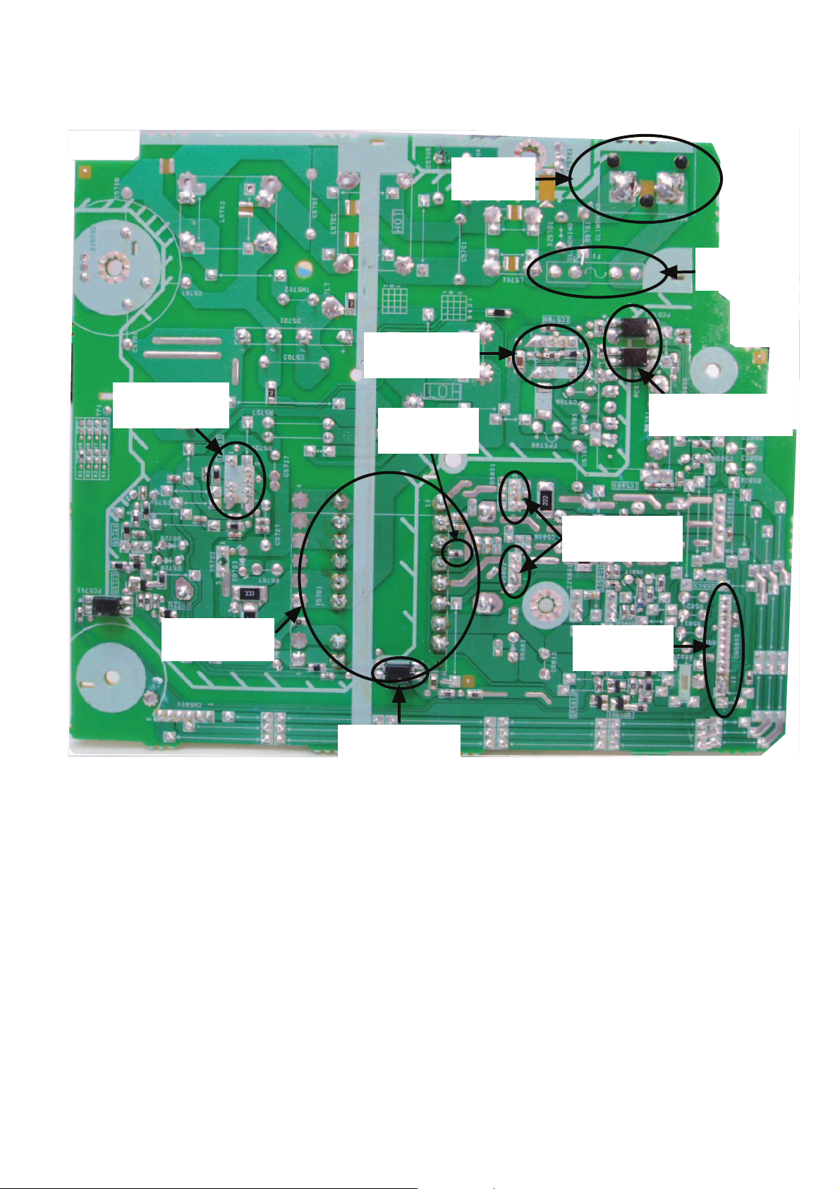
7.2. Part Location
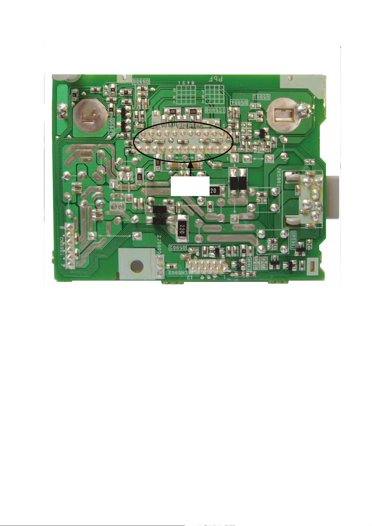
7.2.1. SMPS P.C.B.
AC Inlet:
P5701
Fuse:
F1
Switching IC:
IC5799
Switching IC:
IC5701
Transformer:
T5701
Thermistor:
TH5860
Photocoupler:
PC5720
Fig. 1 SMPS P.C.B.
Photocoupler:
PC5702, PC5799
Rectifier:
D5801, D5802
Connector:
CN5802
23
7.2.2. Main P.C.B.
Voltage Regulator IC:
IC2010
Connector:
CN2014
DC/DC Converter IC:
IC2011
Fig. 2 Main P.C.B.
24
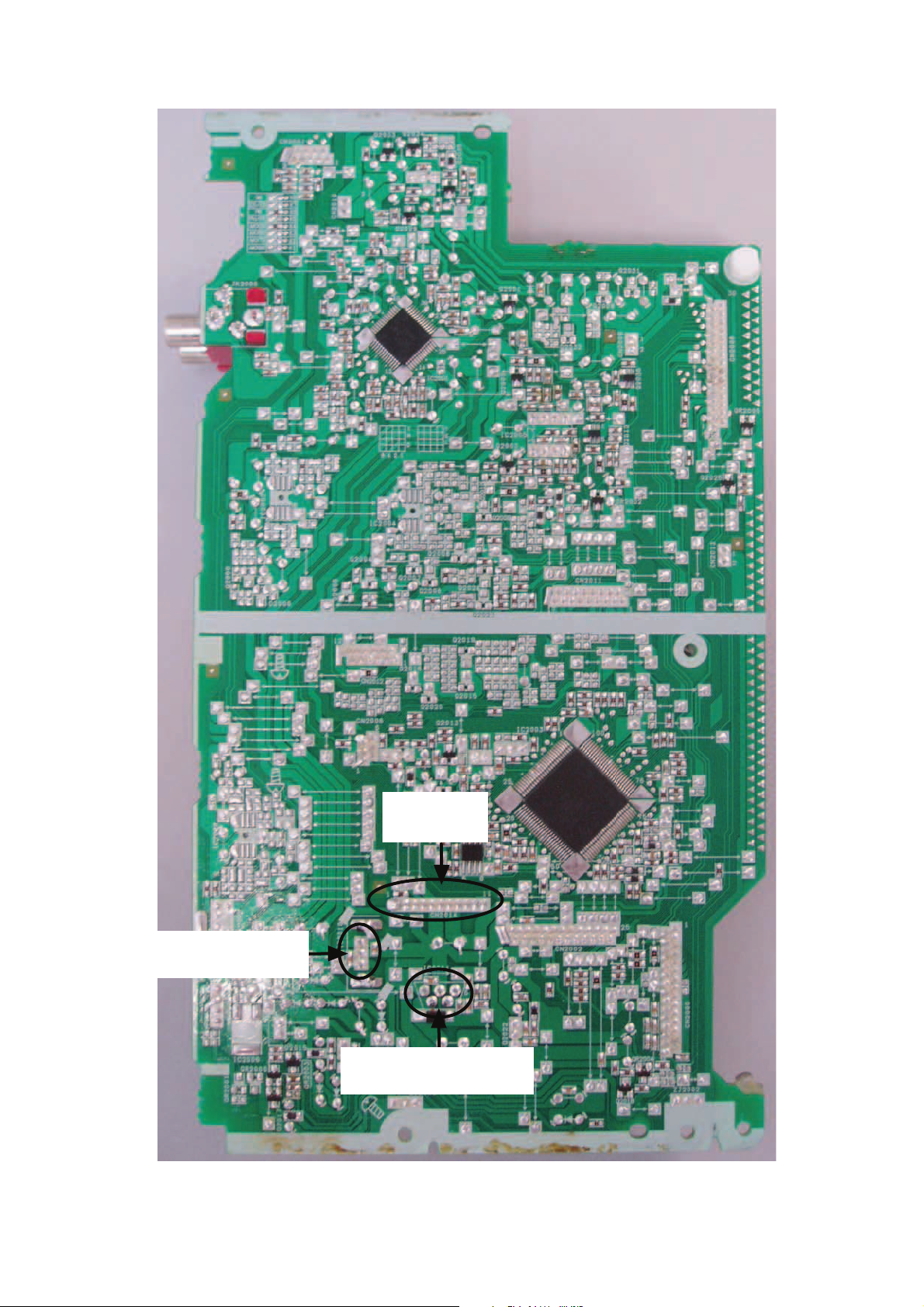
7.2.3. D-Amp P.C.B.
D-Amp IC:
IC5900
Fig. 3 D-Amp P.C.B.
25
7.3. D-Amp IC Operation & Control
D-AMP IC Operation & Control
1) D-AMP IC (C1AB0000497) was used for this model.
2) Three control pins (signal send from micro-processor IC) were used to control the D-AMP IC
operation such as muting, standby and normal operation. They are described as below: -
No Pin no Signal name Function
1 4 F_HOP Frequency Hop control.
2 6 MODE_DA Digital Amp On/Off control.
3 3 MUTE_F Digital Amp Muting control
Table 1: Digital AMP Pin Control.
Here is detailed description of the three control pins for the D-AMP IC
A) MODE_DA & MUTE_F were used to switch the D-AMP IC in the following muting status:
x L(Low/OFF): Standby / OFF
x H (High/ON): Operating or Mute
Below is the logic for the two pins used for the control of the D-AMP IC.
No MODE_DA MUTE_F Digital AMP IC mode status
1 L X OFF (0V)
2 H H Mute (2.5V)
3 H L Operating(5V)
Table 2: Digital AMP IC Mode Status.
Note: Standby/OFF condition of D.AMP IC is available / activated only during the following
event: Switching of Frequency Hoping, power off and start up (when the unit is undergoing
the transition from standby to normal operation mode)
B) F_HOP is used to control the D-AMP operation to avoid interference with AM source by
controlling the frequency source used. It will switch from one frequency to the other, depending on
the tuned AM frequency.
For 9 KHz Step
AM Band Frequency F_HOP Switching Frequency
522 ~ 558 L 301
567 ~ 639 H 350
648 ~ 855 L 301
864 ~ 945 H 350
954 ~ 1152 L 301
1161 ~ 1242 H 350
1251 ~ 1449 L 301
1458 ~ 1539 H 350
1548 ~ 1629 L 301
Table 3: F_HOP Control during 9 kHz Step
For 10 KHz Step
AM Band Frequency F_HOP Switching Frequency
520 ~ 560 L 301
570 ~640 H 350
650 ~ 860 L 301
870 ~ 950 H 350
960 ~ 1160 L 301
26

1170 ~ 1250 H 350
1260 ~ 1450 L 301
1460 ~ 1540 H 350
1550 ~ 1710 L 301
Table 4: F_HOP Control during 10 kHz Step
Note: During activating, the 3 control pins namely MUTE_F, MUTE_A and MODE_DA must
be used to cover the “Pop” sound cause by F-HOP switching.
27

8 Service Fixture & Tools
8.1. Service Tools and Equipment
Prepare service tools before process service position.
Service Tools Remarks
Main P.C.B. (CN2014) - SMPS P.C.B. (CN5802) REXX0189 (11P Cable Wire)
28
9 Disassembly and Assembly Instructions
Caution Note:
• This section describes the disassembly and/or assembly procedures for all major printed circuit boards & main components for the unit. (You ma y refer to the section of “Main components and P.C.B Locations” as described in the service
manual)
• Before carrying out the disassembly process, please ensure all the safety precautions & procedures are followed.
• During the disassembly and/or assembly process, please handle with care as there may be chassis components with
sharp edges.
• Avoid touching heatsinks due to its high temperature after prolong use. (See caution as described below)
• During disassembly and assembly, please ensure proper service tools, equipments o r jigs is being used.
• During replacement of component parts, please refer to the section of “Replacement Parts List” as described in the
service manual.
• Select items from the following indexes when disassembly or replacement are required.
• Disassembly of Top Cabinet
• Disassembly of Tuner P.C.B.
• Disassembly of Front Panel Assembly
• Disassembly of Panel P.C.B.
• Disassembly of Remote Sensor P.C.B.
• Disassembly of CD Open Button P.C.B.
• Disassembly of Jupiter P.C.B.
• Disassembly of Music Port/Headphone P.C.B.
• Disassembly of CD Lid
• Disassembly of Main P.C.B.
• Replacement of Regulator IC (IC2010)
• Disassembly of D-Amp P.C.B.
• Replacement of Audio Digital Amp IC (IC5900)
• Disassembly of SMPS P.C.B.
• Replacement of Switching Regulator IC (IC5701)
• Replacement of Regulator Diode (D5702)
• Replacement of Regulator Diode (D5801)
• Replacement of Regulator Diode (D5802)
• Replacement of Regulator Diode (D5803)
• Disassembly of CD Mechanism Unit (DLS6C)
• Disassembly of CD Servo P.C.B.
• Disassembly of Rear Panel
• Disassembly of Voltage Selector P.C.B. (For PH only)
29
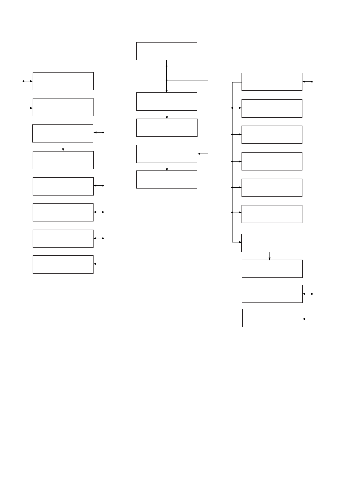
9.1. Disassembly Flow Chart
9.3. Top Cabinet
9.4. Tuner P.C.B.
9.5. Front Panel
Assembly
9.6. Panel P.C.B.
9.7. Remote Sensor
P.C.B.
9.8. CD Open Button
P.C.B.
9.9. Jupiter P.C.B.
Music Port/
9.10.
Headphone P.C.B.
9.12. Main P.C.B.
9.13. Regulator IC
(IC2010)
9.14. D-Amp P.C.B.
9.15. Audio Digital
Amp IC (IC5900)
9.16. SMPS P.C.B.
9.17. Switching Regulator
IC (IC5701)
9.18. Rectifier Diode
(D5702)
9.19. Regulator Diode
(D5801)
9.20. Regulator Diode
(D5802)
9.21. Regulator Diode
(D5803)
9.22. CD Mechanism Unit
(DLS6C)
9.11. CD Lid
9.23. CD Servo P.C.B.
9.24. Rear Panel
9.25.Voltage Selector P.C.B.
(For PH only)
30
 Loading...