

Page 1
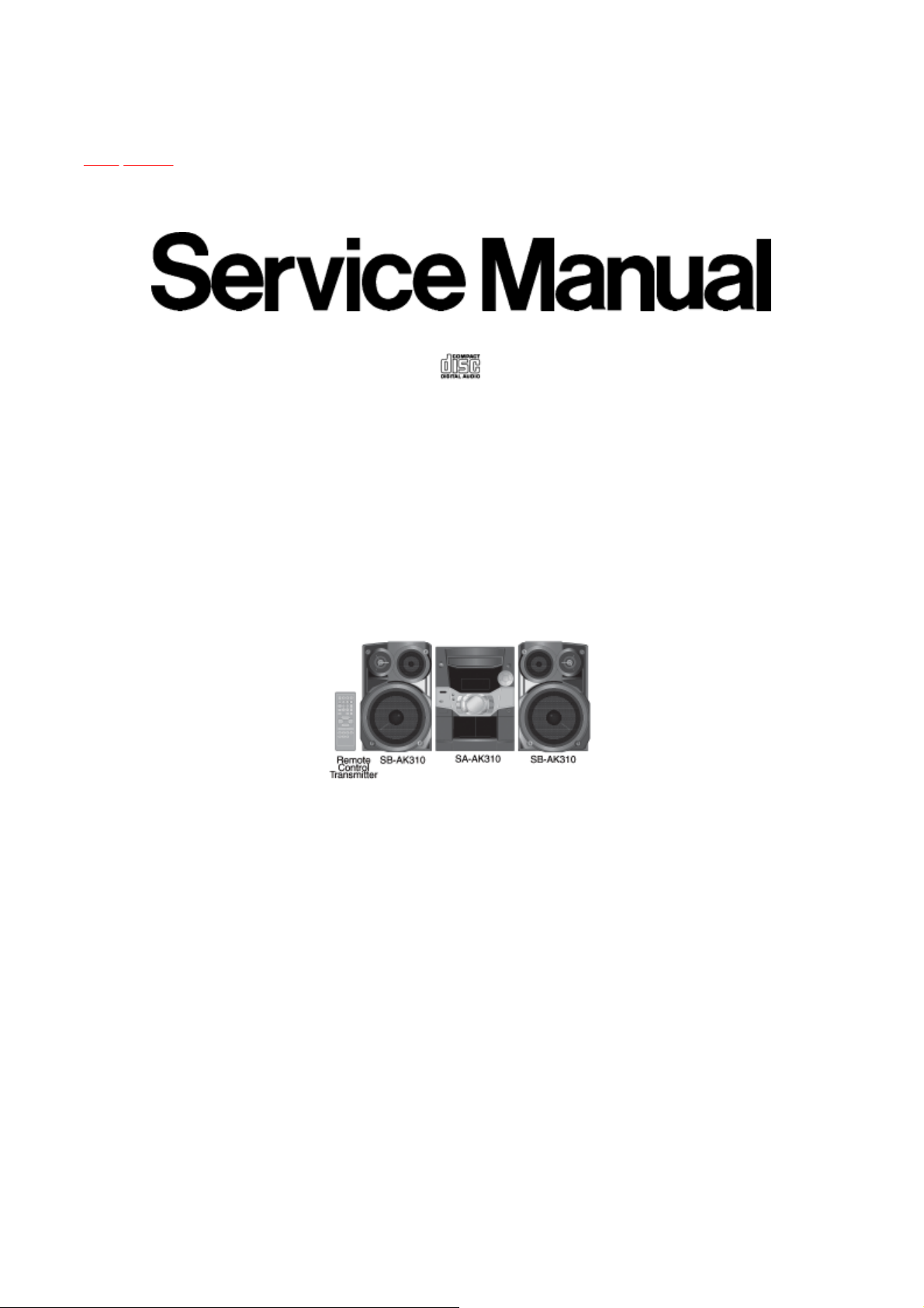
Service Manual
TOP NEXT
ORDER NO. MD0212275C3
CD Stereo System
SA-AK310GC
SA-AK310GN
Colour
(S)... Silver Type
TAPE SECTION :
SG-2W MECHANISM SERIES
Specifications
AMPLIFIER SECTION
Power output
10% Total harmonic distortion
1kHz, both channels driven
(Low channel) 55 W per channel (6Ω )
10kHz, both channels driven
(High channel) 55 W per channel (6Ω )
Total Bi-Amp power 110 W per channel
Input sensitivity
AUX 250 mV
Input Impedance
AUX 13.3 kΩ
FM TUNER SECTION
Frequency range 87.50 - 108.00 MHz (50 kHz steps)
Sensitivity 2.5µ V (IHF)
S/ N 26 dB 2.2µ V
Antenna terminal(s) 75Ω (unbalanced)
AM TUNER SECTION
Frequency range 522 - 1629 kHz (9 kHz steps)
520 - 1630 kHz (10 kHz steps)
Page 2

distribution is a violation of law.
Sensitivity
S/ N 20 dB (at 999 kHz) 560µ V/ m
CASSETTE DECK SECTION
Track system 4 track, 2 channel
Heads
Record/ playback Solid permalloy head
Erasure Double gap ferrite head
Motor DC servo motor
Recording system AC bias 100 kHz
Erasing system AC erase 100 kHz
Tape speed 4.8 cm/ s (1 7/ 8 ips)
Overall frequency response (+ 3 dB, -6 dB at DECK OUT)
NORMAL (TYPE I) 35 Hz - 14 kHz
S/ N 50 dB (A weighted)
Wow and flutter 0.18% (WRMS)
Fast forward and rewind time Approx. 120 seconds with
C-60 cassette tape
CD SECTION
Sampling frequency 44.1 kHz
Decoding 16 bit linear
Beam source/ wave length Semiconductor laser/ 780 nm
Number of channels Stereo
Frequency response 20 Hz - 20 kHz (+ 1, -2 dB)
Wow and flutter Below measurable limit
Digital filter 8 fs
D/ A converter MASH (1 bit DAC)
GENERAL
Power Supply
For GC only AC 110/ 127/ 220-230/ 240 V, 50/ 60Hz
For GN only AC 230-240 V, 50Hz
Power consumption
For GC only 172 W
For GN only 170 W
Power Consumption in standby mode
For GC only 0.85 W
For GN only 0.5 W
Dimensions (W x H x D) 250 x 330 x 370 mm
Mass
For GC only 7.8 kg
For GN only 7.0 kg
SYSTEM
SC-AK310 (GC) Music center: SA -AK310 (GC)
Speaker: SB-AK310 (GC)
SC-AK310 (GN) Music center: SA-AK310 (GN)
Speaker: SB-AK310 (GC)
Notes:
1. Specifications are subject to change without notice. Mass and dimensions are aproximate.
2. Total harmonic distortion is measured by the digital spectrum analyzer.
3. The labels“ HIGH ” and“ LOW” on the rear of the speakers refer to High frequency and Low frequency.
© 2002 Matsushita Electronics (S) Pte. Ltd. All rights reserved. Unauthorized copying and
Page 3

TOP
NEXT
Page 4

1 Before Use
TOP PREVIOUS NEXT
screwdriver to set the voltage selector (on the rear panel) to the voltage setting for the
Note that this unit will be seriously damaged if this setting is not made correctly. (There is no
TOP
PREVIOUS
NEXT
Be sure to disconnect the mains cord before adjusting the voltage selector.
Use a minus(-)
area in which the unit will be used. (If the power supply in your area is 117V or 120V, set to the
“127V” position.)
voltage selector for some countries, the correct voltage is already set.)
Page 5

2 Before Repair and Adjustment
TOP PREVIOUS NEXT
TOP
PREVIOUS
NEXT
Disconnect AC power, discharge Power Supply Capacitors C520 and C540 through a 10Ω, 5W
resistor to ground.
DO NOT SHORT-CIRCUIT DIRECTLY (with a screwdriver blade, for instance), as this may
destroy solid state devices.
After repairs are completed, restore power gradually using a variac, to avoid overcurrent.
Page 6

3 Protection Circuitry
TOP PREVIOUS NEXT
The function of this circuitry is to prevent circuitry damage if, for example, the positive and negative
Note:
TOP
PREVIOUS
NEXT
The protection circuitry may have operated if either of the following conditions are noticed:
No sound is heard when the power is turned on.
Sound stops during a performance.
speaker connection wires are
“shorted”, or if speaker systems with an impedance less than the indicated rated impedance of the
amplifier are used.
If this occurs, follow the procedure outlines below:
1. Turn off the power.
2. Determine the cause of the problem and correct it.
3. Turn on the power once again after one minute.
When the protection circuitry functions, the unit will not operate unless the power is first turned off
and then on again.
Page 7

4 Accessories
TOP PREVIOUS NEXT
TOP
PREVIOUS
NEXT
Remote control transmitter
FM indoor antenna
AC power supply cord (For GC only)
AC power supply cord (For GN only)
AM Loop antenna
Power plug adaptor
Page 8
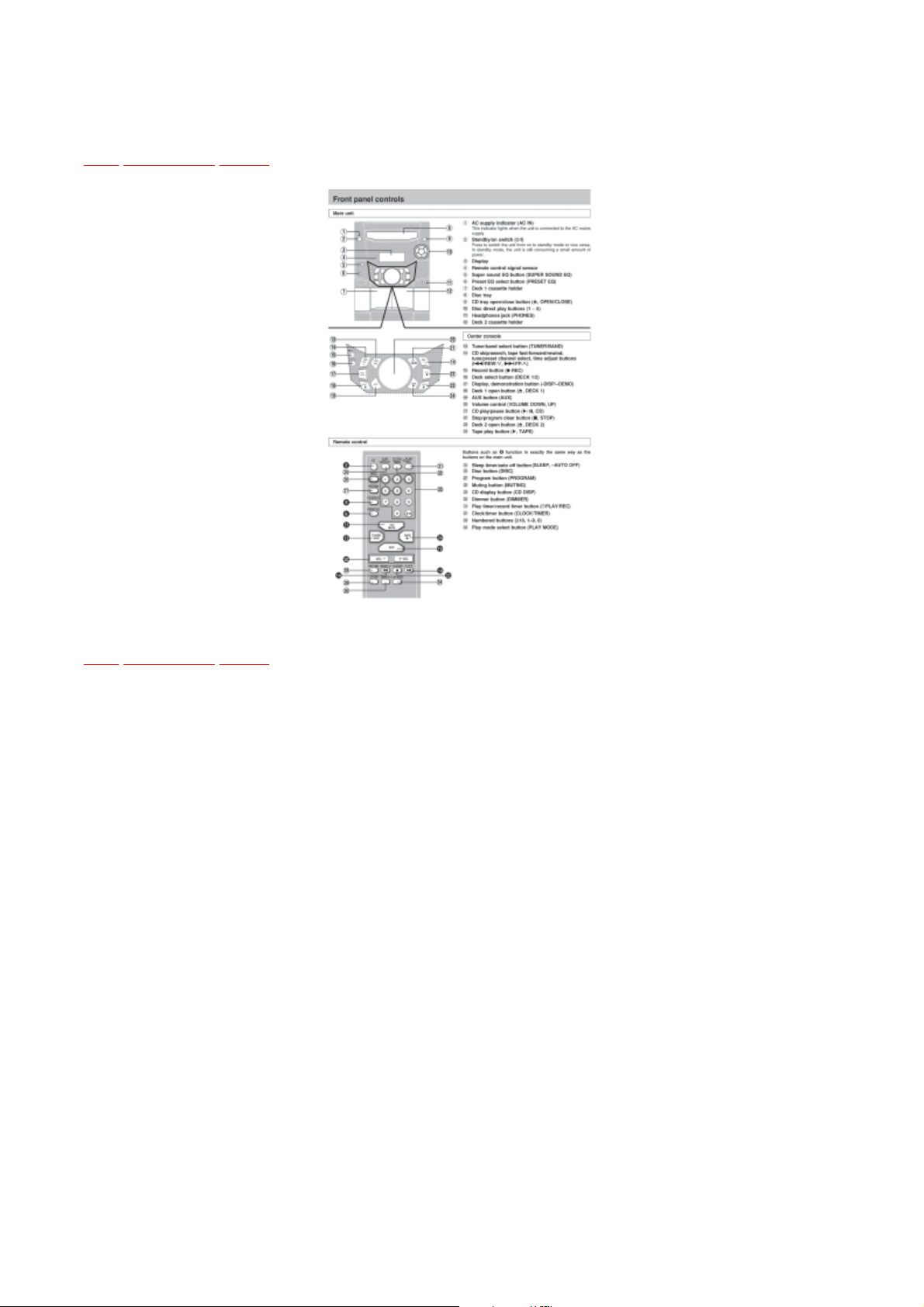
5 Operation Procedures
TOP PREVIOUS NEXT
TOP
PREVIOUS
NEXT
Page 9

6 Handling Precautions For Traverse Deck
TOP PREVIOUS NEXT
Do not subject the traverse deck (optical pickup) to static electricity as it is extremely sensitive
The static electricity of your clothes will not be grounded through the wrist strap. So, take care
connections.
The laser diode in the traverse deck (optical pickup) may break down due to potential difference
caused by static electricity of clothes or human body.
So, be careful of electrostatic breakdown during repair of the traverse deck (optical pickup).
Handling of traverse deck (optical pickup)
1.
to electrical shock.
2. The short land between the No.4(LD) and No.5(GND) pins on the flexible board (FFC) is
shorted with a solder build-up to prevent damage to the laser diode.To connect to the PC
board, be sure to open by removing the solder build-up, and finishthe workquickly.
3. Take care not to apply excessive stress to the flexible board (FFC).
4. Do not turn the variable resistor (laser power adjustment). It has already been adjusted.
Grounding for electrostatic breakdown prevention
1. Human body grounding
Use the anti-static wrist strap to discharge the static electricity from your body.
2. Work table grounding
Put a conductive material (sheet) or steel sheet on the area where the traverse deck
(optical pickup) is placed, and ground the sheet.
Caution :
not to let your clothes touch the traverse deck (optical pickup).
Caution when Replacing the Traverse Deck :
The traverse deck has a short point shorted with solder to protect the laer diode against
electroststics breakdown. Be sure to remove the solder from the short point before making
Page 10

TOP
PREVIOUS
NEXT
Page 11
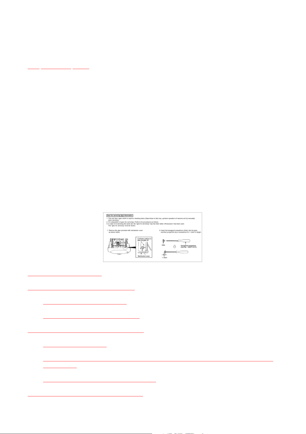
7 Operation Checks and Component
Replacement Procedures
7.4 Main Component Replacement Procedures
TOP PREVIOUS NEXT
“ATTENTION SERVICER”
Some chassis components may have sharp edges.
Be careful when disassembling and servicing.
1. This section describes procedures for checking the operation of the major printed circuit
boards and replacing the main components.
2. For reassembly after operation checks or replacement, reverse the respective procedures.
Special reassembly procedures are described only when required.
3. Select items from the following index when checks or replacement are required.
Warning:
This product uses a laser diode. Refer to caution statement Precaution of Laser Diode.
7.1 Checking for Main P.C.B.
7.2 Disassembly for the CD changer ass ’ y
7.2.1 Disassembly for the CD Lid
7.2.2 Disassembly for CD changer unit
7.3 Checking for the unit operational condition
7.3.1 Initial setting of CD
7.3.2 Checking for the CD Servo P.C.B., Panel P.C.B., Deck P.C.B., Transformer P.C.B. and
Power P.C.B.
7.3.3 Replacement of the Power Amplifier IC
Page 12

7.4.1 Replacement of the Traverse Deck
7.5 Replacement for the disc tray
TOP
PREVIOUS
NEXT
7.6 Disassembly and reassembly for mechanism base drive unit
7.7 Replacement for the motor ass ’ y
7.8 Replacement for the pinch roller ass ’ y and head block
7.9 Replacement for the Deck motor ass ’ y, capstan belt A, capstan belt B and winding belt
7.10 Replacement for the CD motor ass ’ y, capstan belt A, capstan belt B and winding belt
7.11 Replacement for the cassette lid ass ’ y
7.12 Measure for tape trouble
Page 13
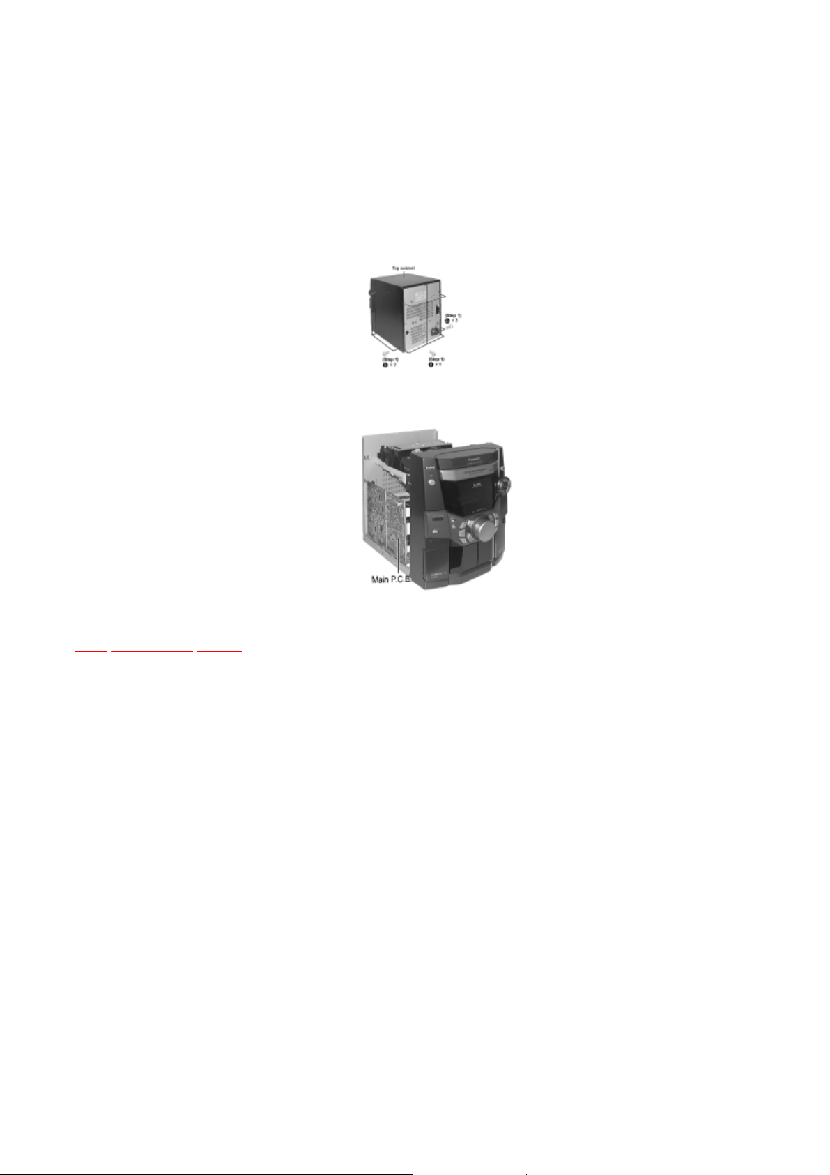
7.1 Checking for Main P.C.B.
TOP PREVIOUS NEXT
TOP
PREVIOUS
NEXT
Step 1 Remove 3 screws each side and 5 screws at rear panel.
Step 2 Lift up both sides of cabinet ass’y, push the cabinet ass’y toward the rear and remove the
cabinet ass’y.
Checking the Main P.C.B. as shown below.
Page 14

7.2 Disassembly for the CD changer ass
’ y
TOP PREVIOUS NEXT
TOP
PREVIOUS
NEXT
(The CD changer unit can be removed after the CD Lid is removed)
7.2.1 Disassembly for the CD Lid
7.2.2 Disassembly for CD changer unit
Page 15

7.2.1 Disassembly for the CD Lid
TOP PREVIOUS NEXT
Step 6
Press the OPEN/CLOSE button, the disc tray will be close.
Follow the (Step 1) - (Step 2) of Item 7.1.
When opening the disc tray automatically (Using Power Supply)
Step 1 Connect the AC power cord.
Step 2 Press the POWER button to power up the main unit.
Step 3 Press the OPEN/CLOSE button, the disc tray will be open automatically.
Step 4 Release the 2 claws, and then remove the CD Lid.
Step 5 Press the POWER button to turn the power on.
Page 16
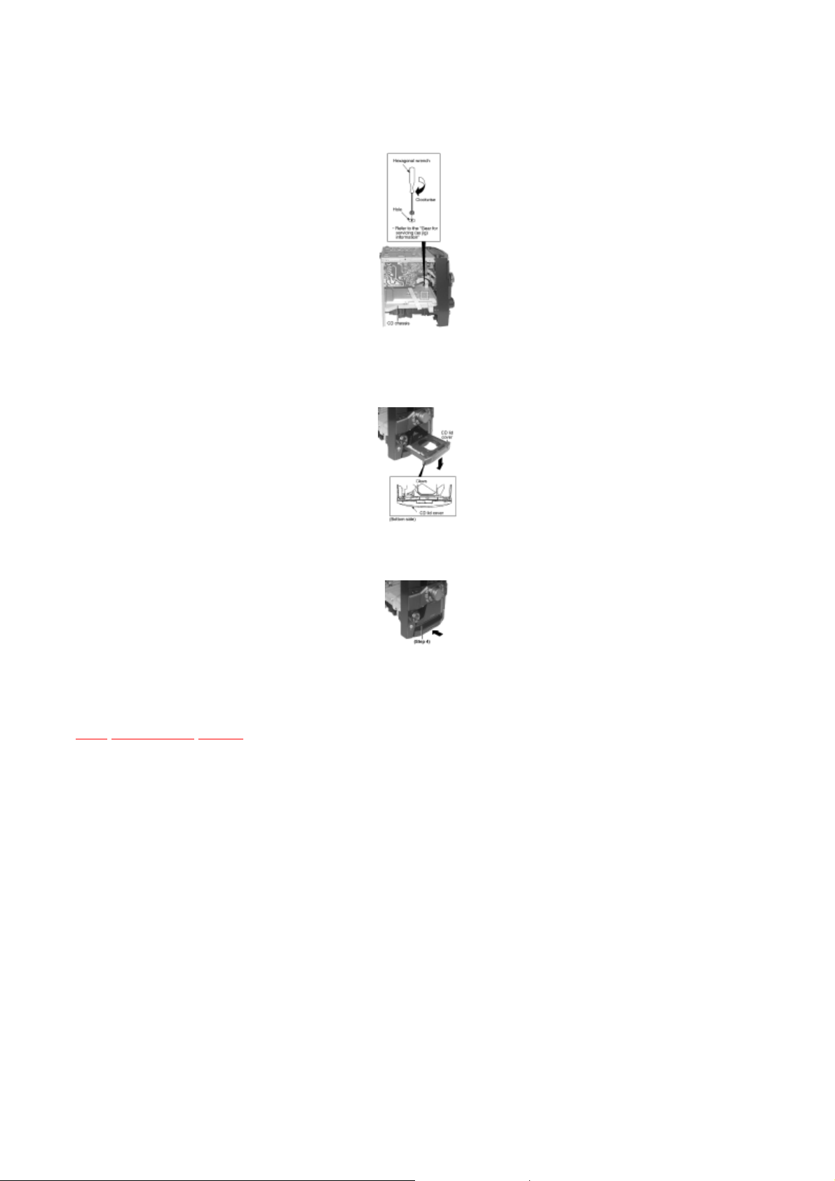
[Open the disc tray manually (Using service tools)]
Step 1 Upset the unit as shown below.
Insert the gear tool into the hole on the underside of CD chasis and then rotate in the direction
TOP
PREVIOUS
NEXT
Step 2
of arrow. The disc tray will be open.
Step 3 Release the 2 claws, and then remove the CD lid cover.
Step 4 Push the disc tray.
Page 17
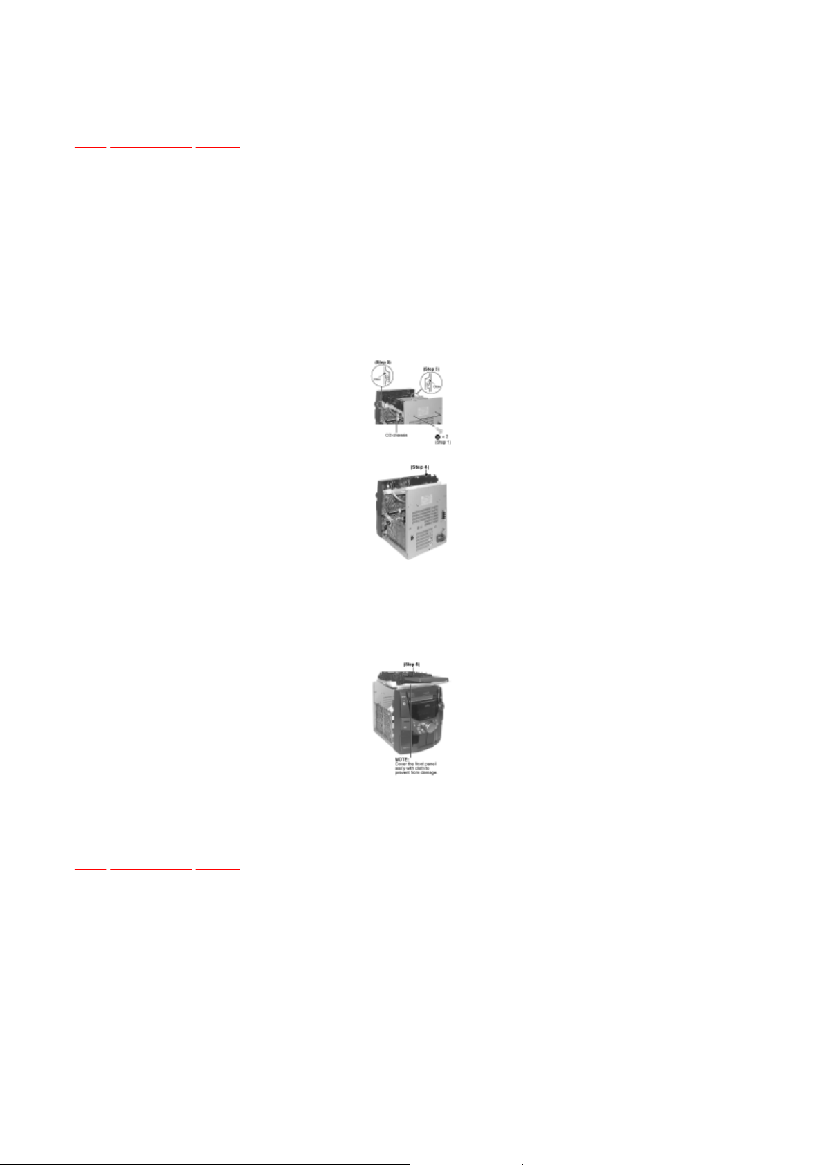
7.2.2 Disassembly for CD changer unit
TOP PREVIOUS NEXT
TOP
PREVIOUS
NEXT
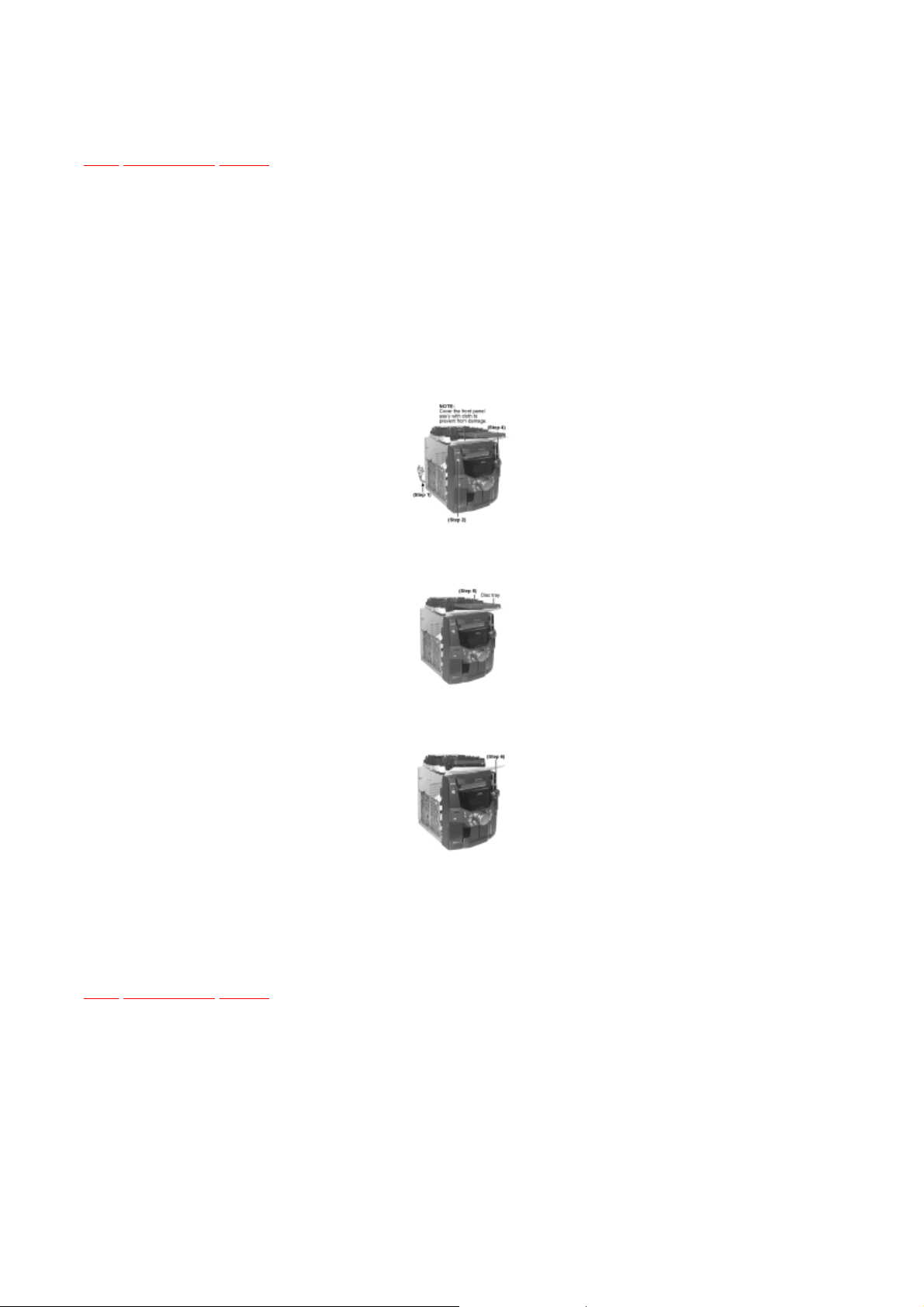
Follow the (Step 1) - (Step 2) of Item 7.1.
Follow the Disassembly for the CD Lid of Item 7.2.1.
Step 1 Remove 2 screws at rear cabinet as show below.
Step 2 Lift up the mechanism unit cover, and then push in the mechanism unit cover.
Step 3 Release the claws of both ends, and then lift up the CD changer unit.
Step 4 Upset the CD changer unit.
Step 5 Place the CD changer unit on the unit.
<The preparation of checking procedures in operational condition is completed>
Page 18

7.3 Checking for the unit operational condition
TOP PREVIOUS NEXT
TOP
PREVIOUS
NEXT
(Place the unit horizontally when loading the CD changer unit.)
7.3.1 Initial setting of CD
7.3.2 Checking for the CD Servo P.C.B., Panel P.C.B., Deck P.C.B., Transformer P.C.B. and Power
P.C.B.
7.3.3 Replacement of the Power Amplifier IC
Page 19
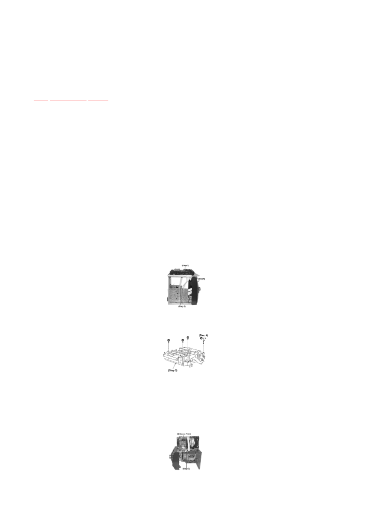
7.3.1 Initial setting of CD
TOP PREVIOUS NEXT
TOP
PREVIOUS
NEXT
Follow the (Step 1) - (Step 2) of Item 7.1.
Follow the Disassembly for the CD Lid of Item 7.2.1.
Step 1 Connect the AC power cord.
Step 2 Press POWER button to turn on power for main unit.
Step 3 Select the input select button to “CD”.
Step 4 Push the OPEN/CLOSE button, and then open the disc tray.
Step 5 Put the CD into the disc tray.
Step 6 Press the OPEN/CLOSE button 1, and then close the disc tray. (Then, the CD will load.)
<The initial setting of CD unit is completed.>
Page 20
7.3.2 Checking for the CD Servo P.C.B., Panel
P.C.B., Deck P.C.B., Transformer P.C.B. and
The initial setting of CD unit must be completed. (Refer to the initial setting of CD unit in item
Step 7
Connect the FFC board (19 pin) from CD servo P.C.B..
Power P.C.B.
TOP PREVIOUS NEXT
Follow the (Step 1) - (Step 2) of Item 7.1.
Follow the Disassembly for the CD Lid of Item 7.2.1.
The initial setting of CD unit must be completed. (Refer to the initial setting of CD unit in
Item 7.3.1).
Check for CD Servo P.C.B.
7.3.1.)
Step 1 Push the power button and the power turns OFF.
Step 2 Remove the FFC boards.
Step 3 Remove the CD changer unit.
Step 4 Remove 4 screws.
Step 5 Remove the mechanism unit cover.
Check the CD Servo P.C.B. as shown below
Step 6 Lay the unit.
Page 21
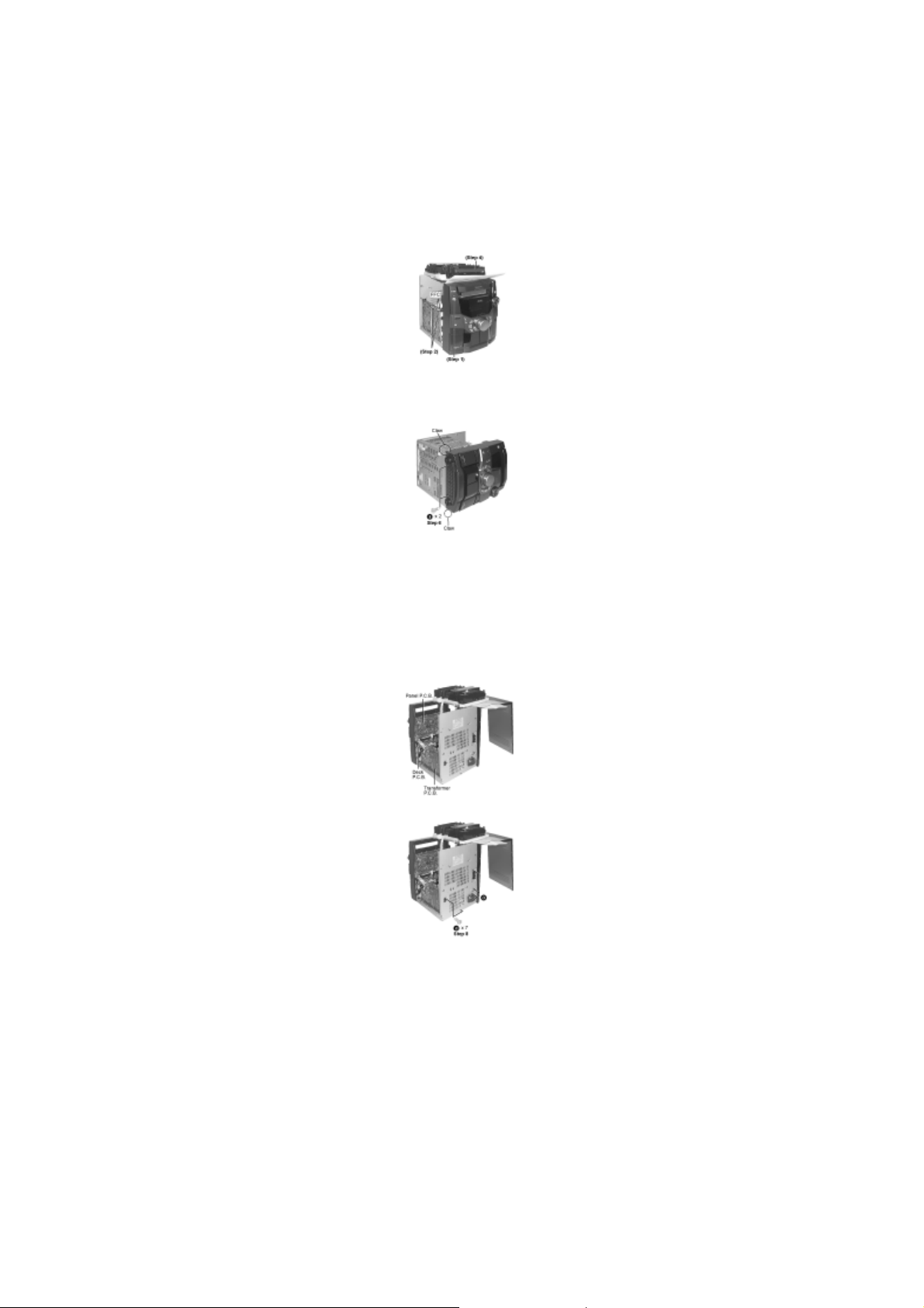
Step 1
Press the POWER button and the power turns off.
Step 2 Remove the connectors.
and Power P.C.B. of Item 7.3.2.
Step 3 Pull out the FFCs.
Step 4 Remove the CD changer unit.
Step 5 Lay the unit as shown below.
Step 6 Remove 2 screws.
Step 7 Release the 2 claws, and then draw the front panel ass’y.
Check the Panel P.C.B., Deck P.C.B. and Transformer P.C.B. as shown below
Step 8 Release the 6 screws, and then remove the rear cover.
Checking the Power P.C.B. as shown below
Follow the (Step 1) - (Step 2) of Item 7.1.
Follow the (Step 1) - (Step 6) of Disassembly for the CD Lid of Item 7.2.1.
Follow the (Step 1) - (Step 8) of Checking for Panel P.C.B.,Deck P.C.B., Transformer P.C.B.
Page 22
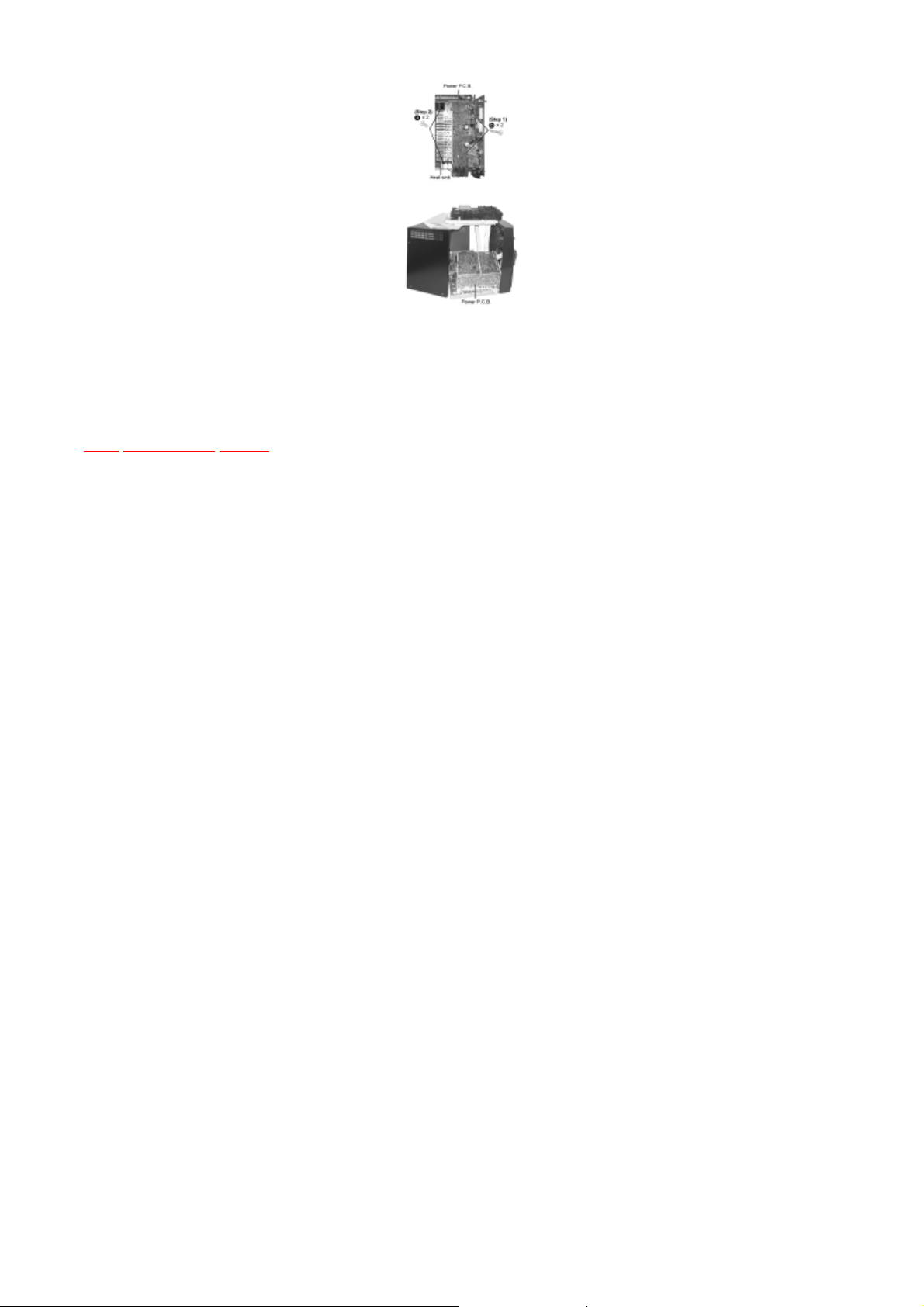
NOTE:
TOP
PREVIOUS
NEXT
Insulate Power P.C.B. with insulation material to avoid short circuit.
Page 23
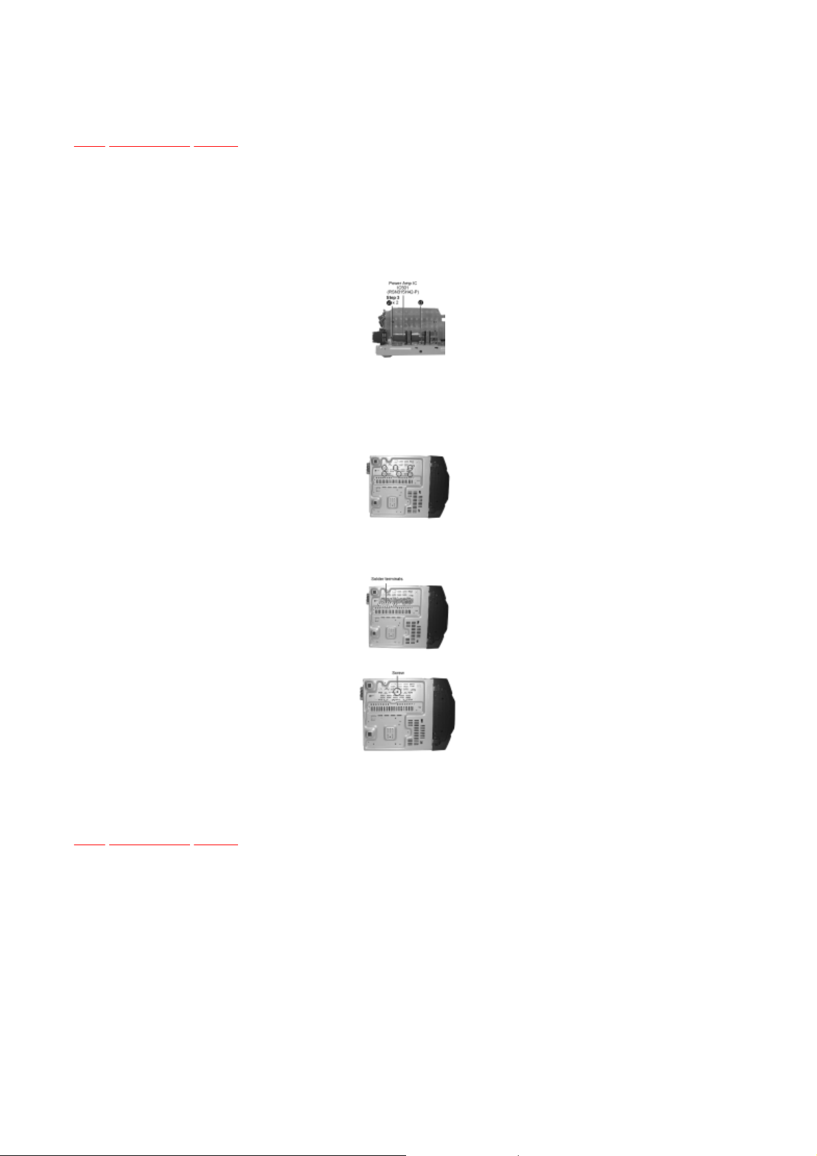
7.3.3 Replacement of the Power Amplifier IC
TOP PREVIOUS NEXT
TOP
PREVIOUS
NEXT
Checking the Power P.C.B.
Follow the (Step 1) - (Step 2) of Item 7.1.
Step 1 Remove the 2 screws fixed to the Power Amplifier IC.
Step 2 Remove 2 screws fixed to the Power Amplifier IC and Transistor Holders.
Step 3 Break the joint with a metal cutter as shown below.
Step 4 Unsolder the terminals of Power Amp IC, transistor and replace the component.
Step 5 Fix back the chasis with a screw as shown.
Page 24

7.4 Main Component Replacement Procedures
TOP PREVIOUS NEXT
TOP
PREVIOUS
NEXT
7.4.1 Replacement of the Traverse Deck
Page 25
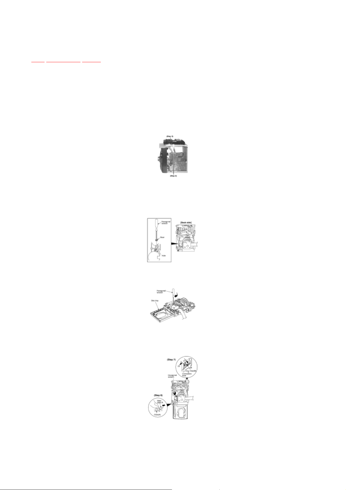
7.4.1 Replacement of the Traverse Deck
TOP PREVIOUS NEXT
Rotate the hexagonal wrench in the direction of arrow (clockwise), and then open the disc tray
for a little amount.)
Follow the (Step 1) - (Step 2) of Item 7.1.
Follow the (Step 1) - (Step 6) of Disassembly for the CD Lid of Item 7.2.1.
Follow the disassembly instruction for the CD changer unit of Item 7.2.2.
Step 1 Push the power button and the power turns OFF.
Step 2 Remove the FFC boards.
Step 3 Remove the CD changer unit.
Step 4 Insert the gear with hexagonal wrench into the hole.
Step 5
fully.
Step 6 With pressing the claw (A), rotate the hexagonal wrench clockwise. (The slide plate R moves
Page 26
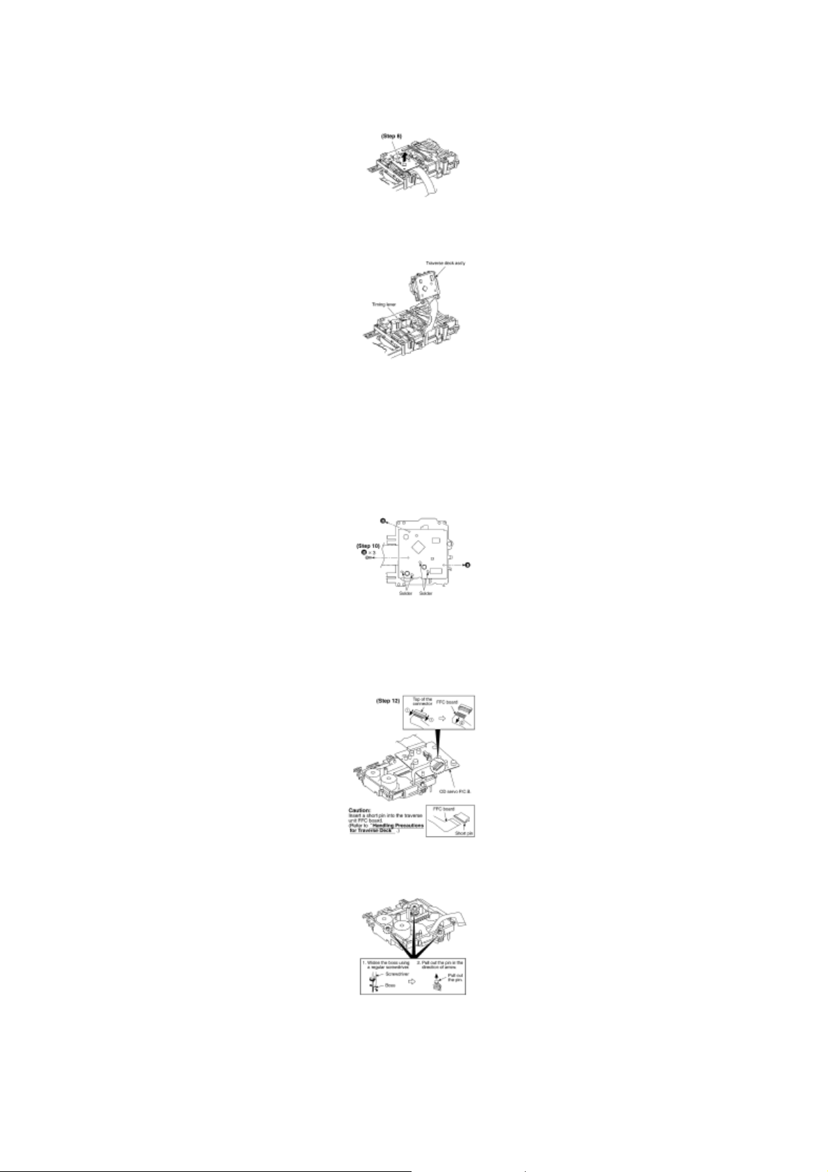
Step 7
Pressing the claw (B) in the direction of arrow (1), the connection lever moves in the direction
of arrow (2).
Step 13
Remove the pin.
Step 8 Lift up the traverse deck ass’y.
Step 9 Remove the traverse deck ass’y from the timing lever.
Caution:
When removing or inserting the traverse deck avoid touching the OPU lens and pressing onto the
turntable.
Step 10 Remove 3 screws.
Step 11 Unsolder the motor terminals (4 points).
Step 12 Remove the FFC board from the connector, and then remove the CD Servo P.C.B.
Page 27

Note:
Step 2
Align the boss of traverse deck ass
’
y with the slot of traverse cam gear.
Step 14 Release the claw, and then remove the traverse deck ass’y.
Be careful not to lose the 3 floating spring because those will also be removed on removal of the
traverse deck ass’y.
Installation of the CD Servo P.C.B. after replacement
Step 1 Connect the FFC board.
Step 2 Install the CD servo P.C.B. in the traverse deck ass’y.
Step 3 Remove 3 screws.
Step 4 Solder.
Note for installation of the CD servo P.C.B.
Installation for traverse deck ass’y
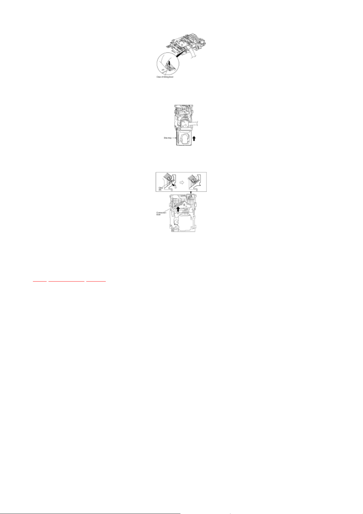
Step 1 Install the traverse deck ass’y to the timing lever.
Page 28
TOP
PREVIOUS
NEXT
Step 3 Force the claw of timing lever.
Step 4 Force the disc tray fully.
Step 5 With pressing the claw (B) in the direction of arrow (1), force the connection lever in the
direction of arrow (2).
Page 29
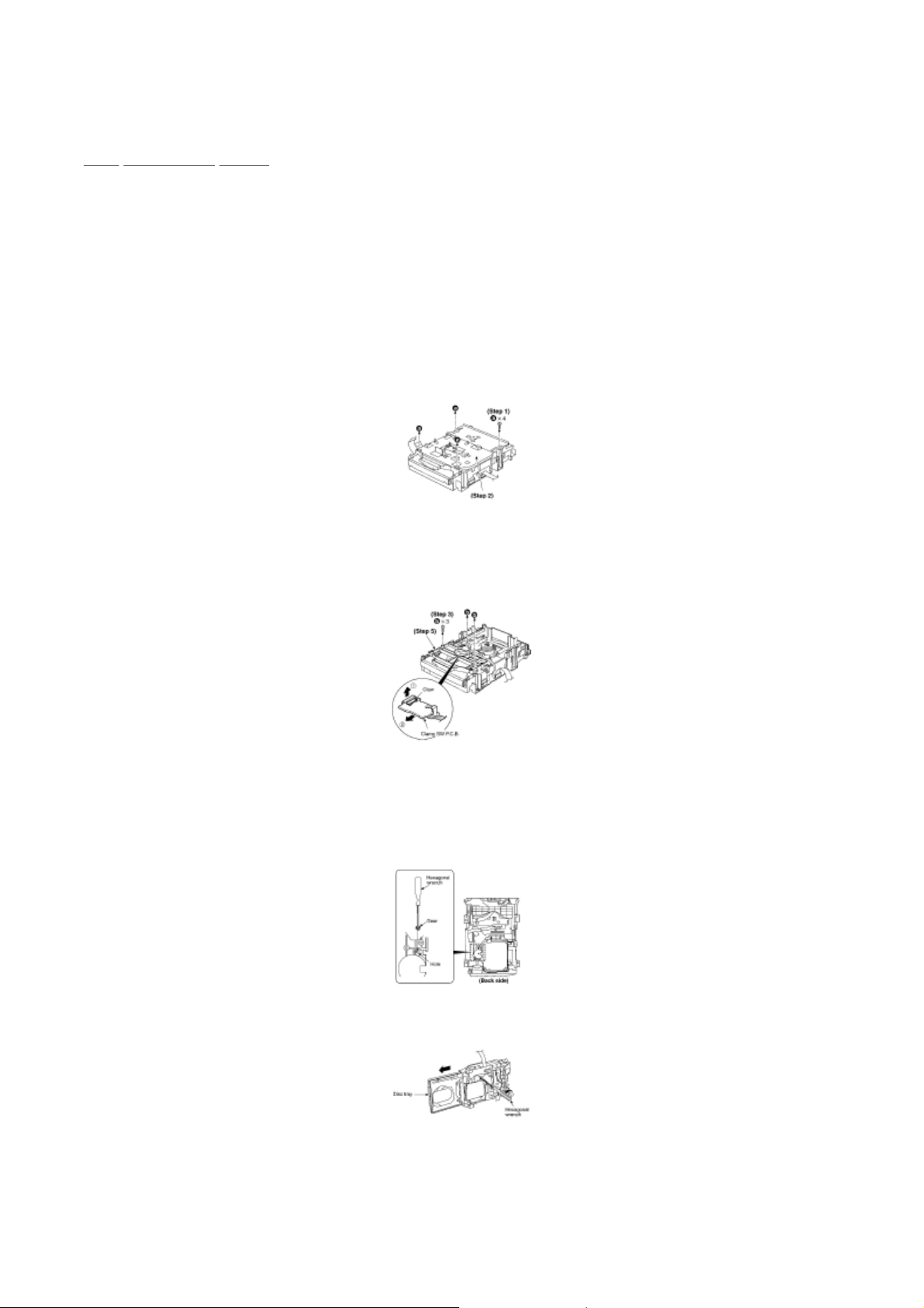
7.5 Replacement for the disc tray
TOP PREVIOUS NEXT
Step 7
Rotate the hexagonal wrench in the direction of arrow, and then open the disc tray fully.
Follow the (Step 1) - (Step 2) of Item 7.1
Follow the Disassembly for the CD Lid of Item 7.2.1.
Follow the Disassembly for the CD Changer Unit of Item 7.2.2.
Follow the (Step 1) - (Step 8) of Item 7.4
Step 1 Remove 4 screws.
Step 2 Remove the upper plate.
Step 3 Remove 3 screws.
Step 4 With lifting the claw in the direction of (1), draw the clamp SW P.C.B. in the direction of
arrow (2).
Step 5 Remove the mechanism cover.
Step 6 Insert the gear with hexagonal wrench into the hole.
Page 30
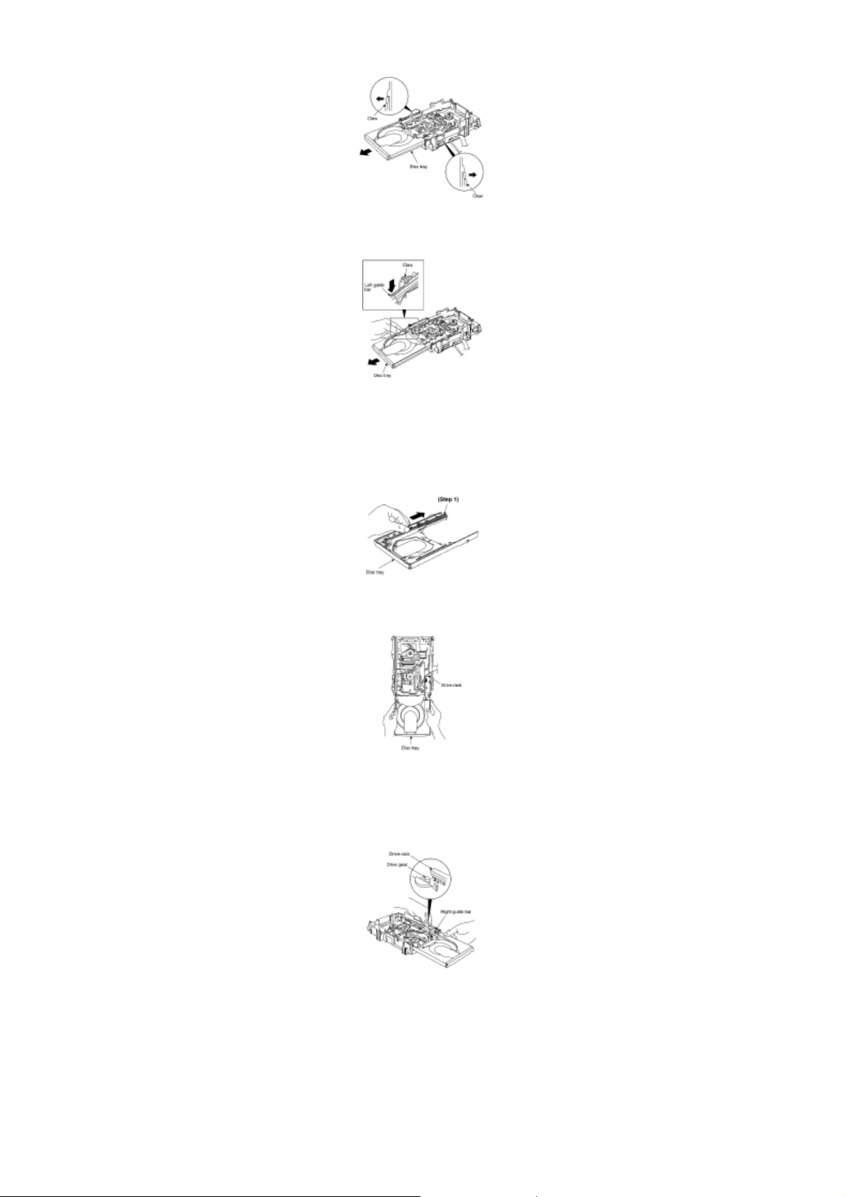
NOTE:
Force the right guide bar of tray base manually not to move upwards.
Step 8 Release the both claws, and then draw the disc tray.
Step 9 With forcing the left guide bar manually because the left guide bar interfers with claw, draw
the disc tray.
[Installation of the disc tray after replacement]
Step 1 Slide the drive rack fully in the direction of arrow.
Step 2 Holding the drive rack not to move, install the disc tray.
Step 3 Align the drive rack with the drive gear.
Page 31

TOP
PREVIOUS
NEXT
Step 4 Holding the disc tray manually, push the disc tray in the direction of the arrow.
Page 32
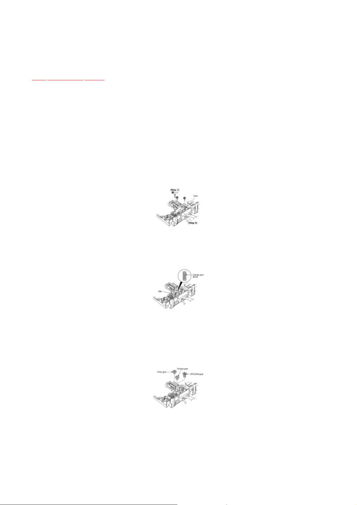
7.6 Disassembly and reassembly for mechanism
base drive unit
NOTE:
Step 5
Release the 2 claws, and then remove the bottom SW P.C.B..
TOP PREVIOUS NEXT
Follow the (Step 1) - (Step 2) of Item 7.1.
Follow the Disassembly for the CD Lid of Item 7.2.1.
Follow the Disassembly for the CD changer unit of Item 7.2.2.
Follow the (Step 1) - (Step 14) of Item 7.4
Follow the (Step 1) - (Step 9) of Item 7.5
Step 1 Remove 3 screws.
Step 2 Release the claw, and then remove the gear holder.
Step 3 Remove the belt and change gear spring.
Take care not to lose the change gear spring.
Step 4 Remove the pulley gear, change gear and UP/DOWN gear.
Page 33
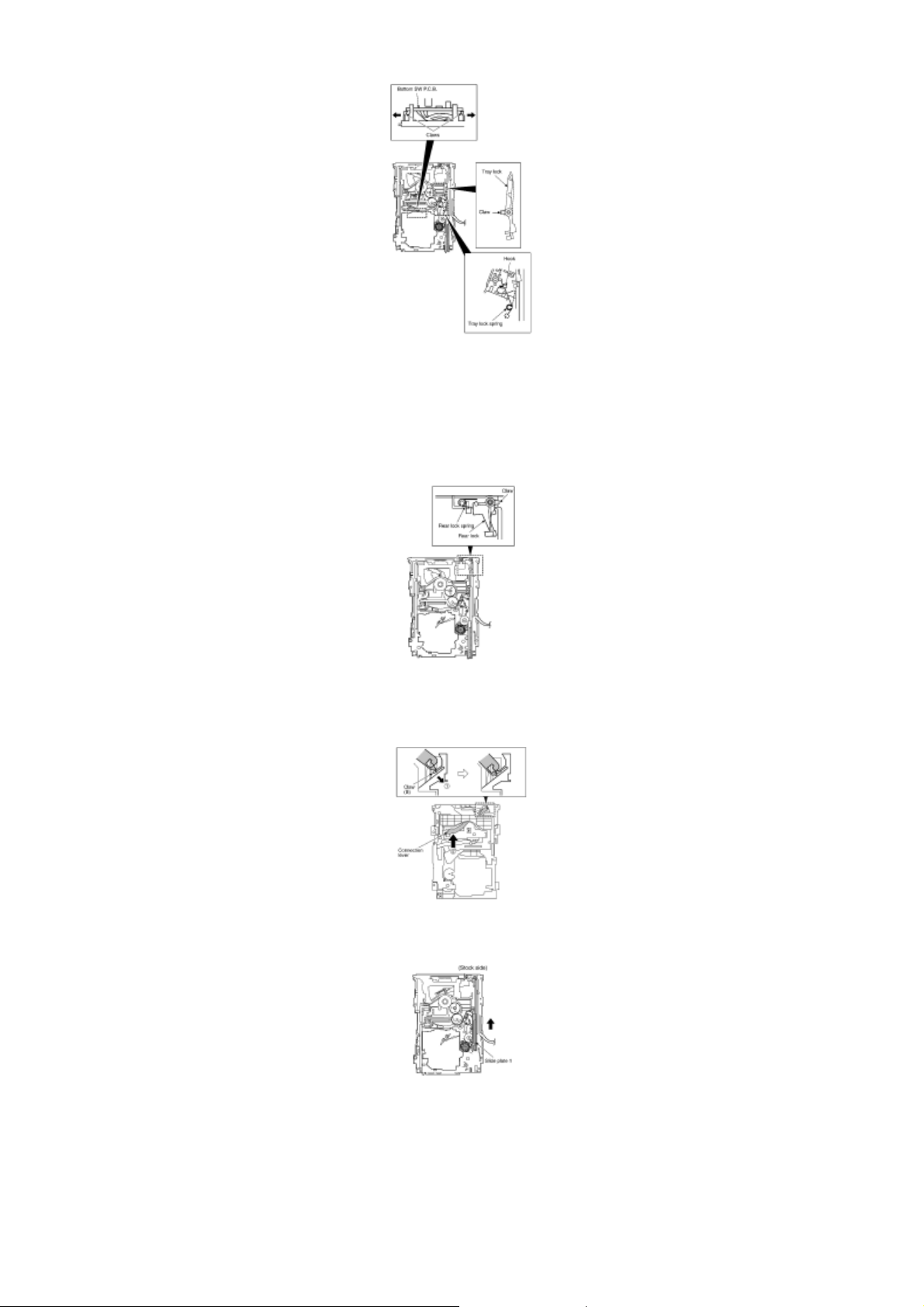
unit in the direction of arrow (2).
Step 6 Install the tray lock spring to hook temporary.
Step 7 Release the claw, and then remove the tray lock.
Step 8 Release the claw, and then remove the rear lock.
Step 9 Pressing the claw (B) in the direction of arrow (1), force the connection lever in the direction
of arrow (2).
Step 10 Move the slide plate 1 to the end of stock side.
Step 11 Lift up the left end of spindle base unit in the direction of arrow (1), and then remove the
Page 34
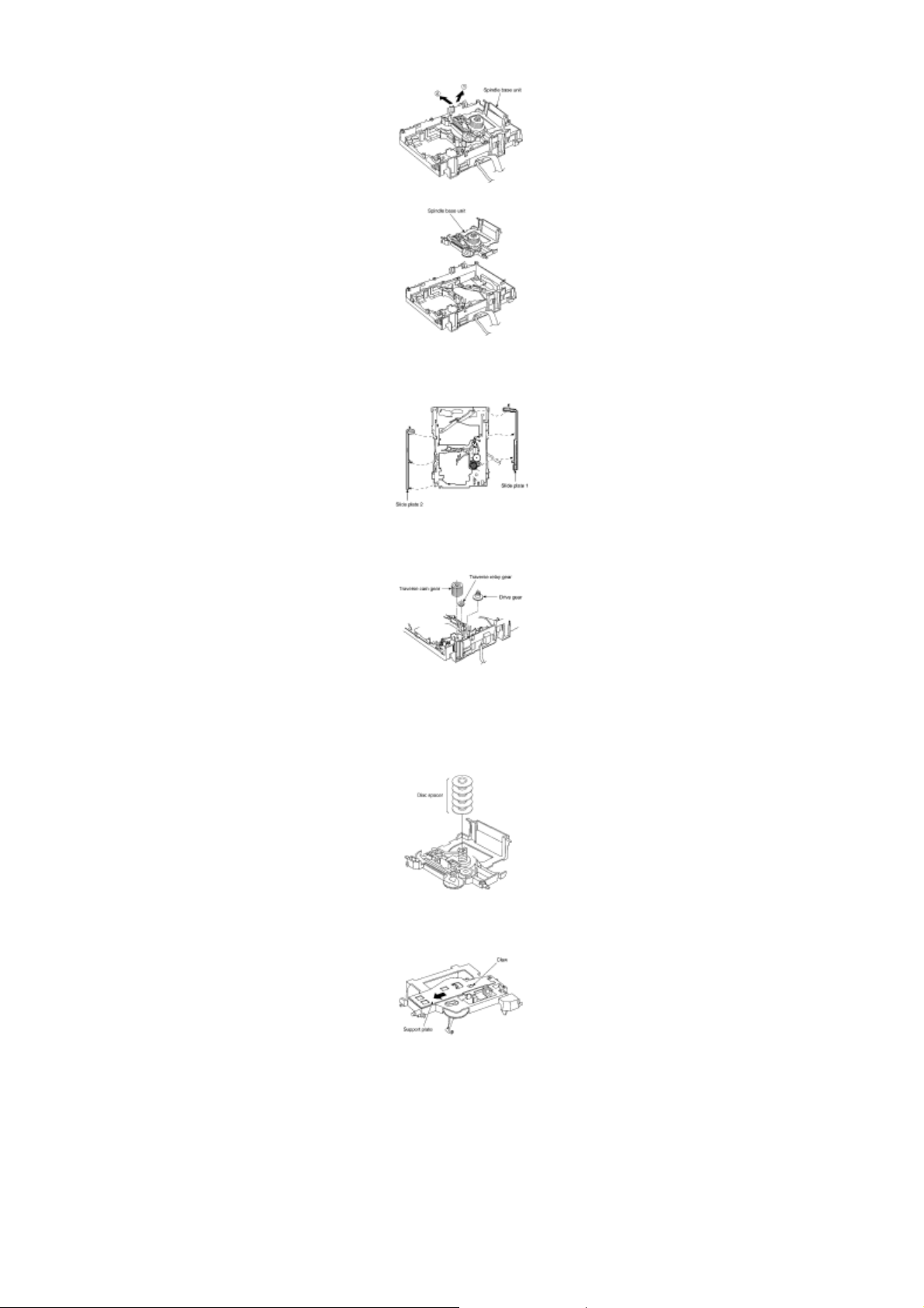
Step 3
Rotate the disc lever in the direction of arrow (1), draw the disc lever.
Step 12 Remove slide plate 1 and slide plate 2.
Step 13 Remove the traverse relay gear, traverse cam gear and drive gear.
[Dissassembly/reassembly for the spindle base unit]
Step 1 Draw the 5 disc spacers.
Step 2 Pushing the claw, slide the support plate in the direction of arrow, and then remove it.
Page 35
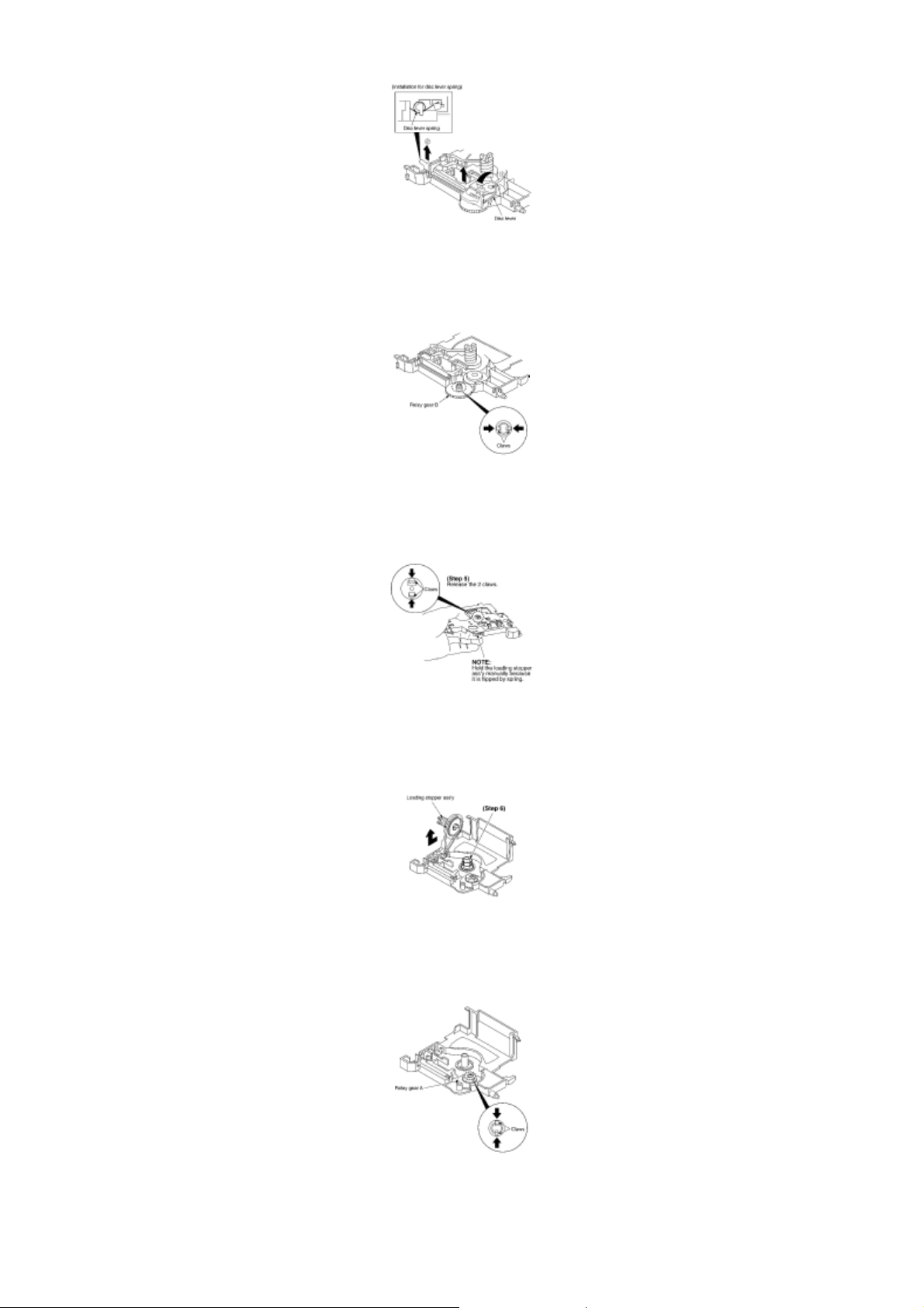
NOTE:
NOTE:
Step 8
Release the 2 claws, and then remove the relay gear A.
Take care not to lose the disc lever spring.
Step 4 Release the 2 claws, and then draw the relay gear B.
Step 5 Release the 2 claws as shown below.
Hold the loading stopper ass’y manually bacause it is flipped by spring.
Step 6 Remove the cushion spring.
Step 7 Remove the loading stopper ass’y in the direction of arrow.
Page 36
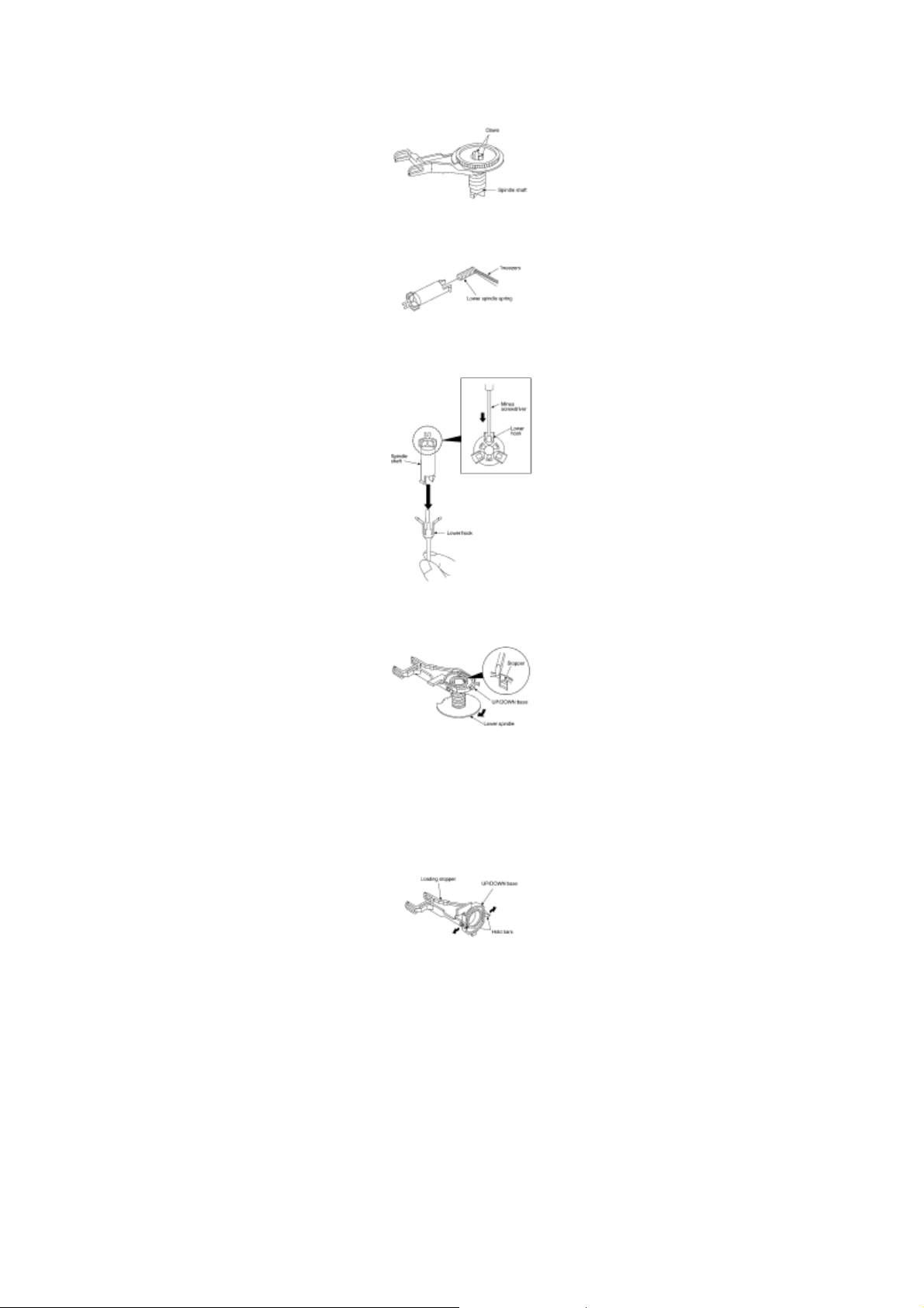
Step 9
Release the 2 claws, and then remove the spindle shaft.
Rotate the UP/DOWN base at a 90° angle. Then, spread the hold bars of loading stopper and
exercised when alignment of claw due to the size of claws.)
Step 10 Remove the lower spindle spring with tweezers.
Step 11 Force the lower hook with thin tip of minus screwdriver.
Step 12 Squeeze the shaft of lower hook, and then draw it.
Step 13 Rotate the lower spindle in the direction of arrow until the lower spindle interferes with
stopper.
Step 14 Insert the thin tip of minus screwdriver between the lower spindle and UP/DOWN base, and
then slacken the lower spindle to release the stopper. Then, rotate the lower spindle and remove it.
Step 15
remove the UP/DOWN base.
[Installation for loading stopper ass’y]
Step 1 Align the claw of loading stoppers ass’y with the slot of spindle base. (Caution should be
Page 37
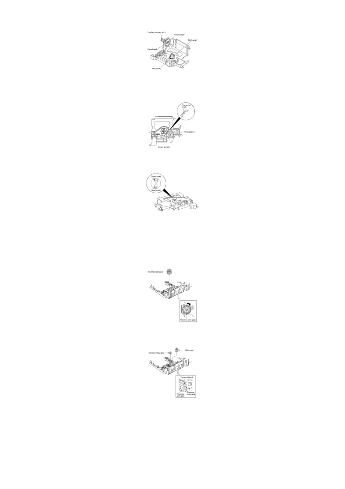
gear.
Step 2 Lower the loading stopper ass’y, and then align the lower spindle with the trapezoid tooth of
relay gear A.
Step 3 Force the loading stopper ass’y, latch the claw firmly.
[Reassembly for mechanism base drive unit]
Step 1 Install the traverse cam gear.
Step 2 Rotate the traverse cam gear to the direction of arrow.
Step 3 Install the drive gear and traverse relay gear.
*When installing the traverse relay gear, align the trapezoid tooth of gear with tooth of traverse cam
Page 38
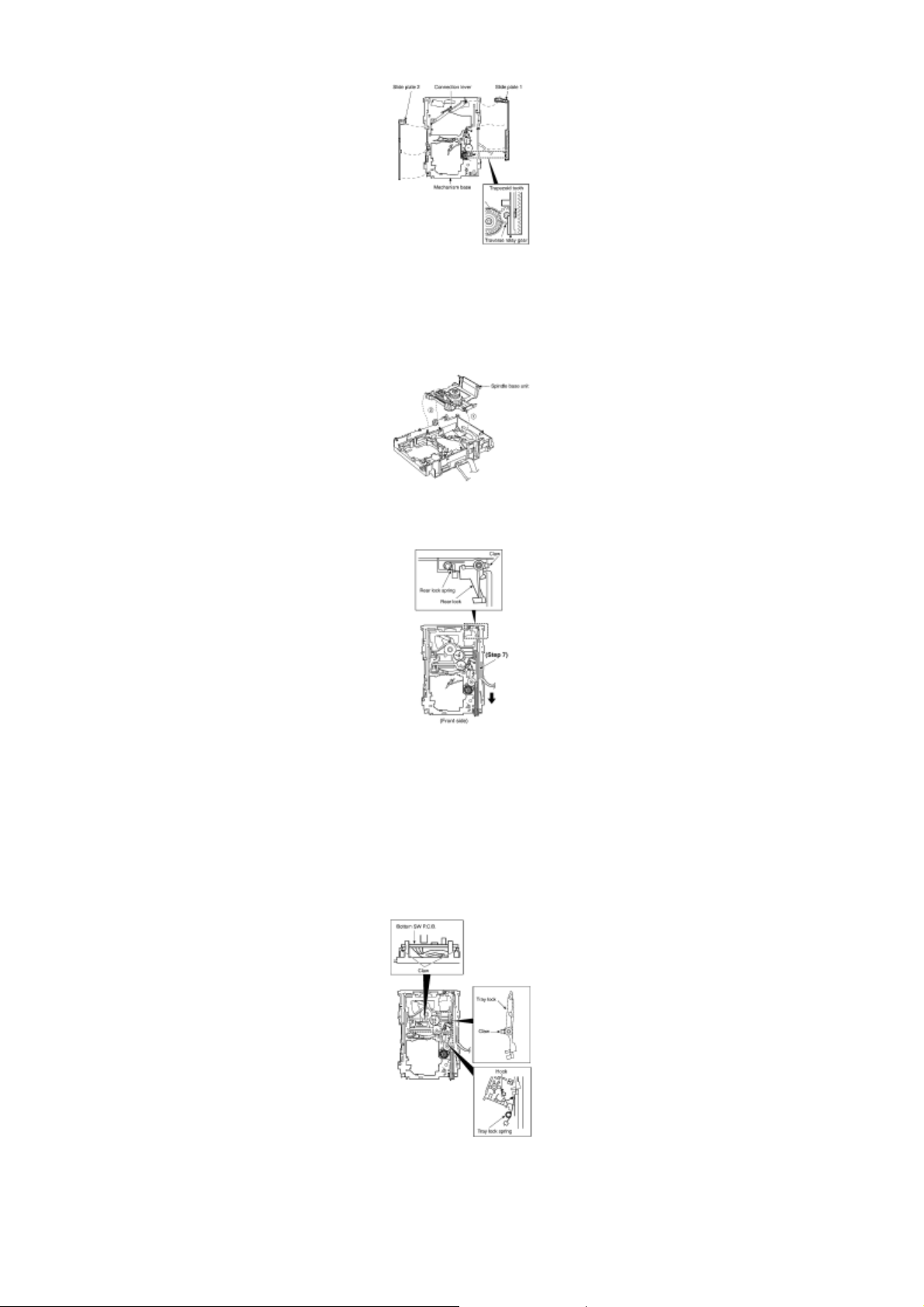
Step 11
Remove the tray lock spring from hook,and then latch to the tray lock.
Step 4 Install the slide plate 2 to the mechanism base, and then match to the connection lever.
Step 5 Install the slide plate 1 to the mechanism base, and then match to the connection leve and
align the trapezoid tooth of traverse relay gear with the slide plate 1.
Step 6 Install the spindle base unit. (First, slide plate 1.)
Step 7 Move the slide plate 1 to forward fully.
Step 8 Install the rear lock. (The claw should be latched.)
Step 9 Install the bottom SW P.C.B.. (The claw should be latched.)
Step 10 Install the tray lock. (The claw should be latched.)
Page 39
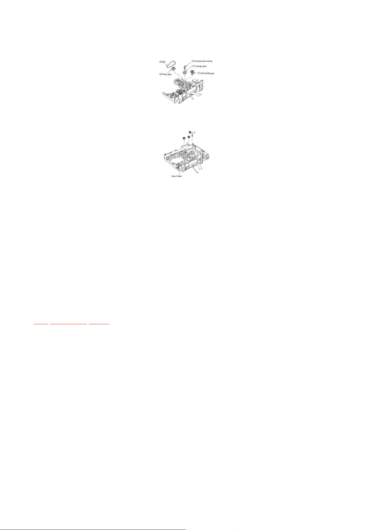
Step 12
Install the UP/DOWN gear, change gear, change gear spring, pulley gear and belt in the
order of (1) - (5).
TOP
PREVIOUS
NEXT
Step 13 Install the gear holder, and then tighten the screw (a).
Step 14 Install the tray base, traverse ass’y, mechanism cover and upper plate.
[Operation check after servicing]
Check the proper operation of following items with gear and hexagonal screwdriver.
1. Open/close of tray base.
2. Moving the tray base to the stock side.
3. UP/DOWN operation of spindle base unit.
4. UP/DOWN operation of traverse ass’y.
Page 40
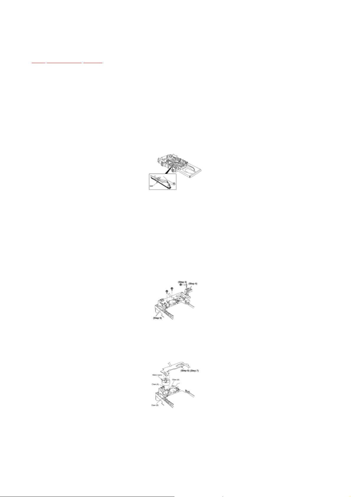
7.7 Replacement for the motor ass
’ y
TOP PREVIOUS NEXT
NOTE:
[Notice for motor ass
’
y installation]
Follow the (Step 1) - (Step 2) of Item 7.1.
Follow the Disassembly for the CD Lid of Item 7.2.1.
Follow the Disassembly for the CD changer unit of Item 7.2.2.
Follow the (Step 1) - (Step 8) of Item 7.4
Follow the (Step 1) - (Step 7) of Item 7.5
Step 1 Install the belt temporarily.
Take care not apply the grease to the belt.
Step 2 Upset the CD loading unit.
Step 3 Remove 3 screws.
Step 4 Unsolder the plunger terminals (2 points).
Step 5 Unsolder the motor terminals (2 points).
Step 6 Release the 2 claws (A), and then remove the Motor P.C.B.
Step 7 Release the claw (B), and then remove the motor ass’y.
Page 41

1.
Locate the name plate of motor to the traverse ass
’y.
2. Align the hole of motor with the ribs.
TOP
PREVIOUS
NEXT
Page 42
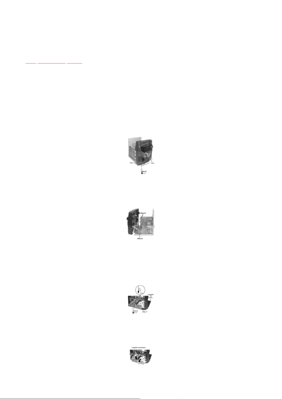
7.8 Replacement for the pinch roller ass
’ y and
head block
TOP PREVIOUS NEXT
Follow the (Step 1) - (Step 2) of Item 7.1.
Follow the Disassembly for the CD Lid of Item 7.2.1.
Follow the disassembly for the CD changer unit of Item 7.2.2.
Follow the (Step 1) - (Step 14) of Item 7.4
Step 1 Remove the connector.
Step 2 Remove 2 screws.
Step 3 Remove the 2 claws, and then draw the front panel ass’y.
Step 4 Pull out the FFC.
Step 5 Remove the flat cable from the connector.
Step 6 Push the lever upward, and then open the cassette lid ass’y (For DECK1 and DECK2).
Step 7 Remove the flat cable from the connector (CN1001).
Step 8 Remove the 5 screw.
Page 43
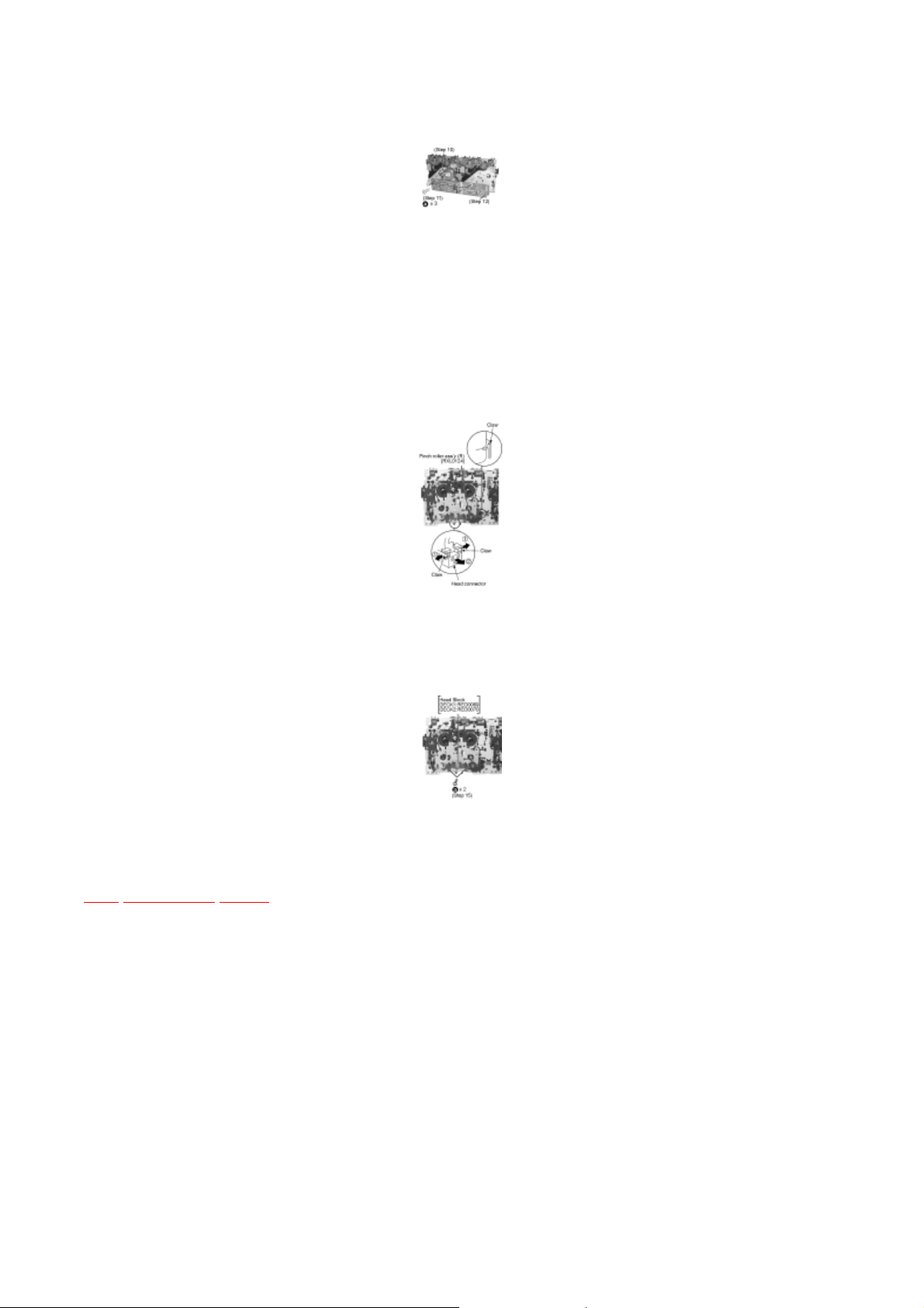
Step 9
Tilt the cassette mechanism in the direction of arrow (1), and then remove it in the direction
of arrow (2).
TOP
PREVIOUS
NEXT
Step 10 Unsolder the motor terminals.
Step 11 Remove 4 screws.
Step 12 Remove mechanism Deck P.C.B.
* The mechanism as shown below is for DECK1. For the one of DECK 2, perform the same
procedures.
Step 13 Release the 2 claws, and then remove the pinch roller (R), (F).
Step 14 Release ther 2 claws, and then remove the head connector.
Step 15 Remove 2 screws.
Page 44
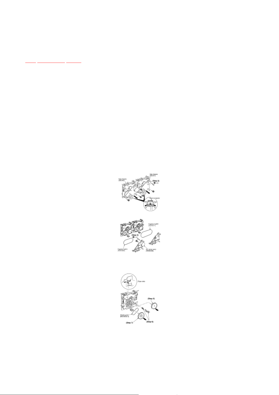
7.9 Replacement for the Deck motor ass
’ y,
capstan belt A, capstan belt B and winding belt
Step 7
Remove the flywheel F.
TOP PREVIOUS NEXT
Follow the (Step 1) - (Step 2) of Item 7.1.
Follow the Disassembly for the CD Lid of Item 7.2.1.
Follow the Disassembly for the CD changer unit of Item 7.2.2.
Follow the (Step 1) - (Step 14) of Item 7.4
Follow the (Step 1) - (Step 11) of Item 7.9
Step 1 Release the 2 claws, and then remove the head connector.
Step 2 Remove 6 screws.
Step 3 Remove the sub chassis.
Step 4 Remove 2 screws.
Step 5 Remove the flywheel R.
Step 6 Release the claw of tape side, and then remove the winding lever and spring.
Page 45
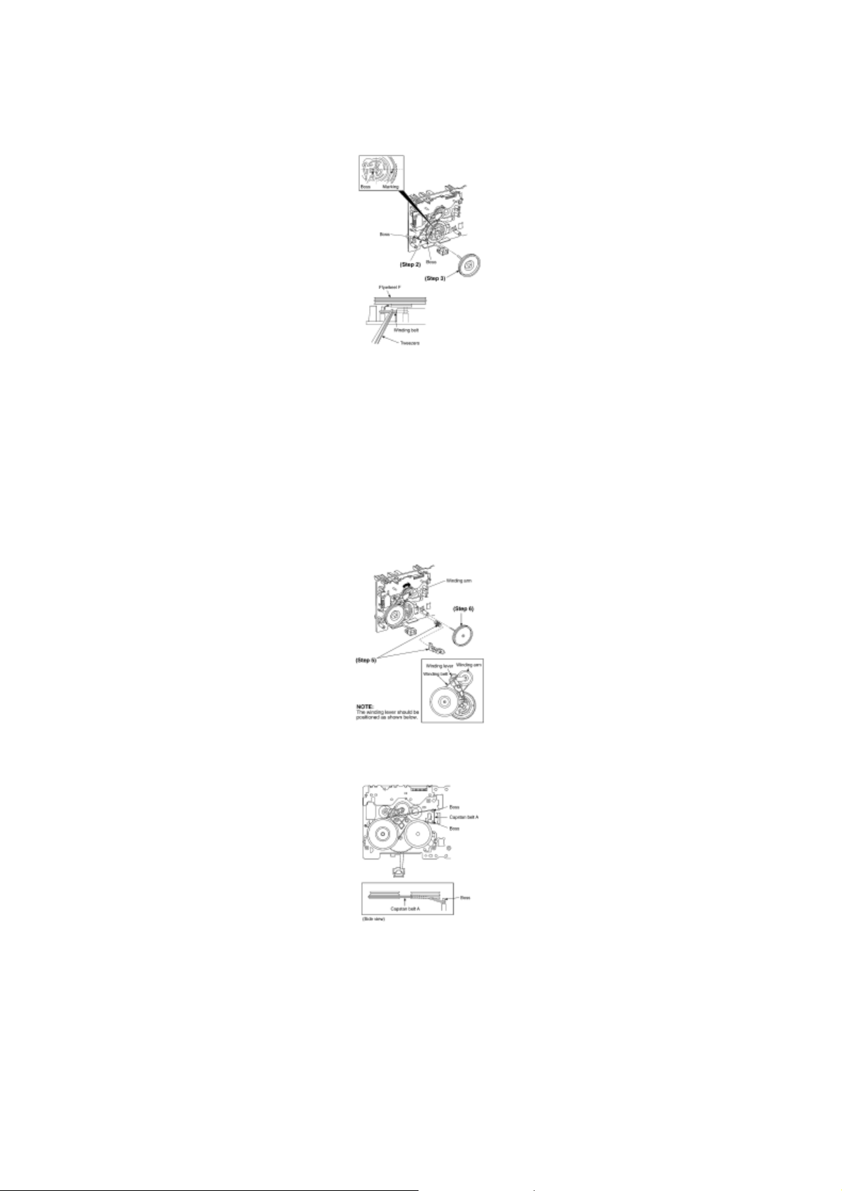
[Installation of the belt]
Step 1 The boss and marking should be positioned horizontally.
Step 9
Install the sub chassis to the mechanism, and then tighten screws.
Step 2 Put the winding belt on the pulley temporarily.
Step 3 Install the flywheel F.
Step 4 Put the winding belt on the flywheel F.
Step 5 Install the winding lever and spring while pressing the winding arm in the direction of arrow.
Step 6 Install the flywheel R.
Step 7 Put the capstan belt A temporarily as shown below.
Step 8 Put the capstan belt B on the motor ass’y pulley.
Page 46
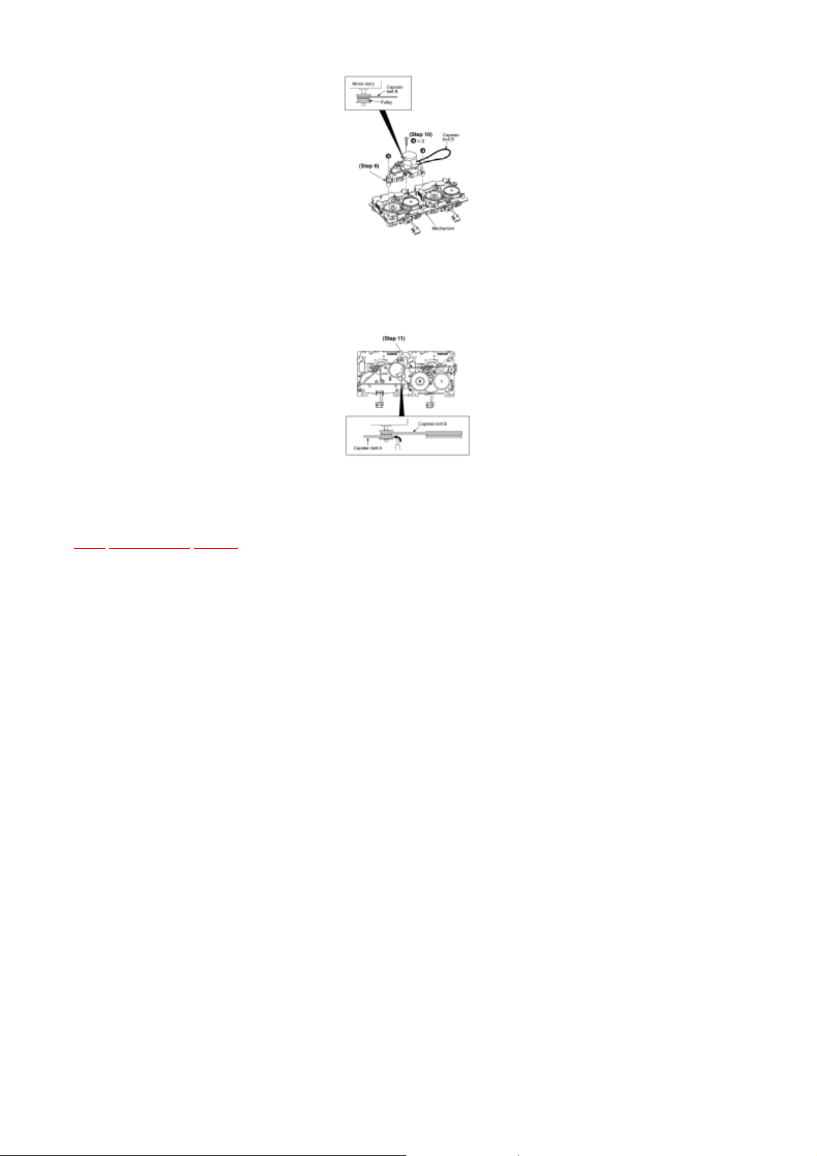
Step 10 Remove 3 screws.
TOP
PREVIOUS
NEXT
Step 11 Put the capstan belt B as shown below.
Step 12 Put the capstan belt A on the motor ass’y pulley.
Page 47
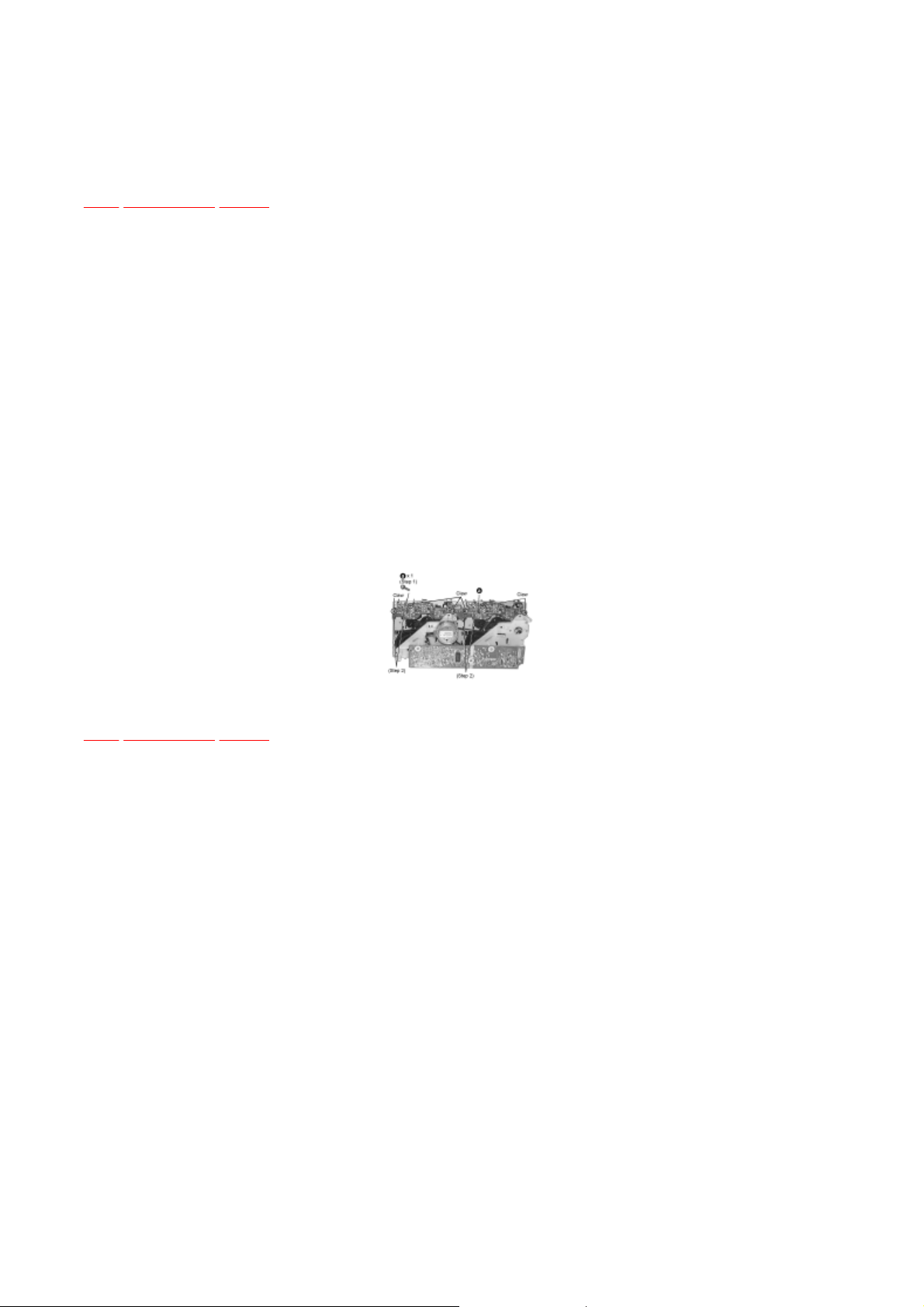
7.10 Replacement for the CD motor ass
’ y,
capstan belt A, capstan belt B and winding belt
TOP
PREVIOUS
NEXT
TOP PREVIOUS NEXT
Follow the (Step 1) - (Step 2) of Item 7.1.
Follow the Disassembly for the CD Lid of Item 7.2.1.
Follow the Disassembly for the CD changer unit of Item 7.2.2.
Follow the (Step 1) - (Step 14) of Item 7.4
Follow the (Step 1) - (Step 11) of Item 7.9
Step 1 Remove 2 screws.
Step 2 Unsolder the plunger terminals (2 points).
Step 3 Release the 3 claws, and then remove the mechanism P.C.B.
Page 48
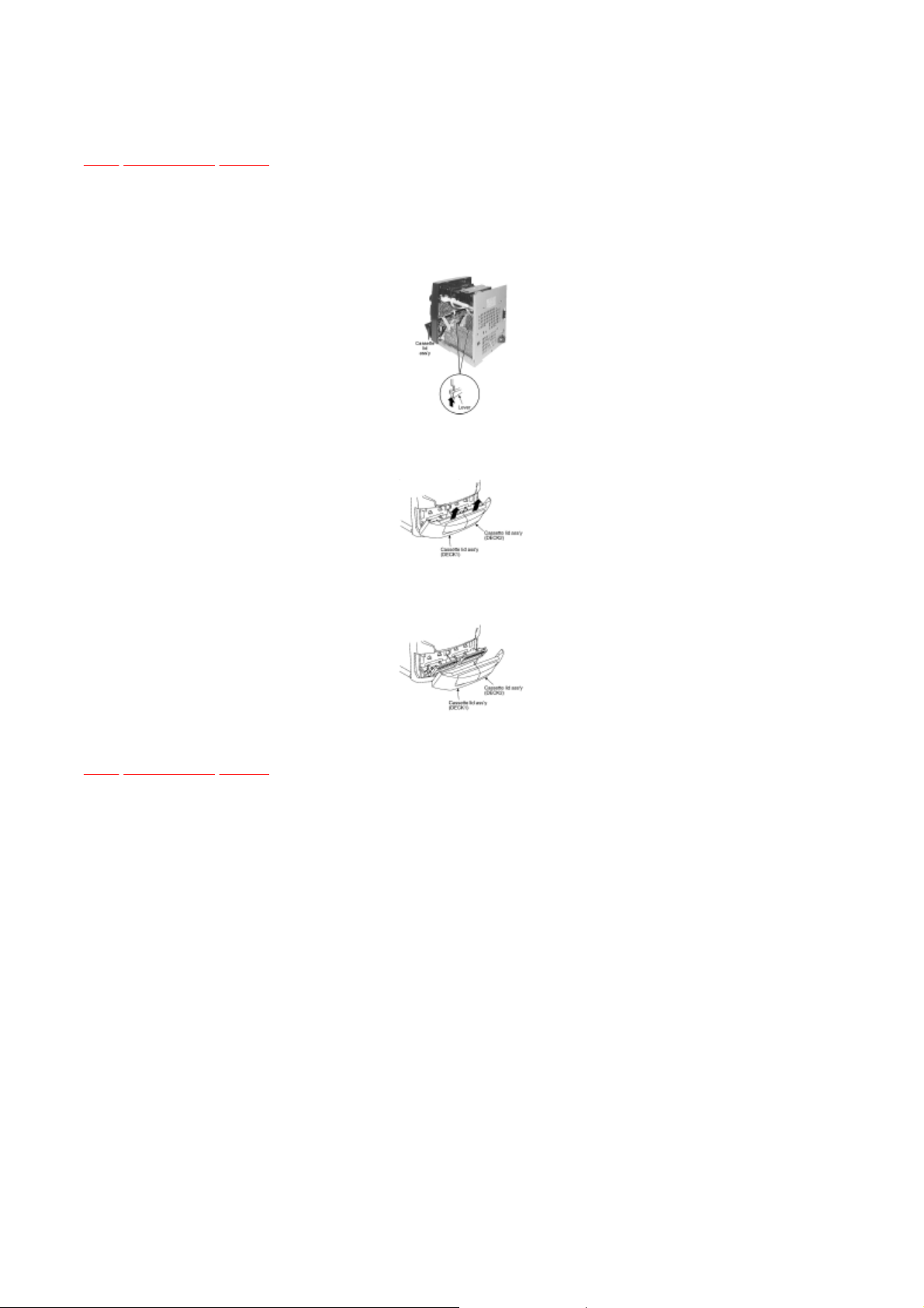
7.11 Replacement for the cassette lid ass
’ y
TOP PREVIOUS NEXT
TOP
PREVIOUS
NEXT
Follow the (Step 1) - (Step 2) of Item 7.1.
Step 1 Force the lever upward, open the cassette lid ass’y. (For DECK1 and DECK2)
Step 2 Lift up the cassette lid ass’y in the direction of arrow. (For DECK1 and DECK2).
Step 3 Remove the cassette lid ass’y. (For DECK1 and DECK2).
Page 49
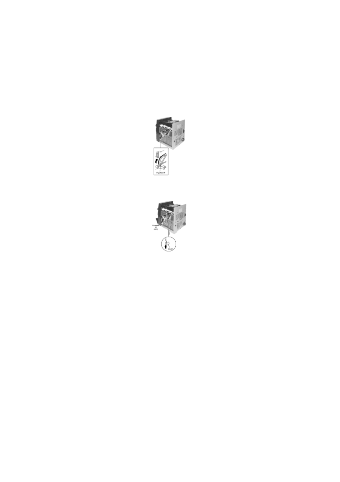
7.12 Measure for tape trouble
TOP PREVIOUS NEXT
TOP
PREVIOUS
NEXT
Follow the (Step 1) - (Step 2) of Item 7.1.
Step 1 If a cassette tape cannot be removed from the deck since the tape is caught by the capstan or
pinch roller during playback or recording, rotate the flywheel F in the direction of the arrow to
remove the tape.
Step 2 Force the lever upward and open the cassette lid ass’y. Take the cassette tape off.
Page 50
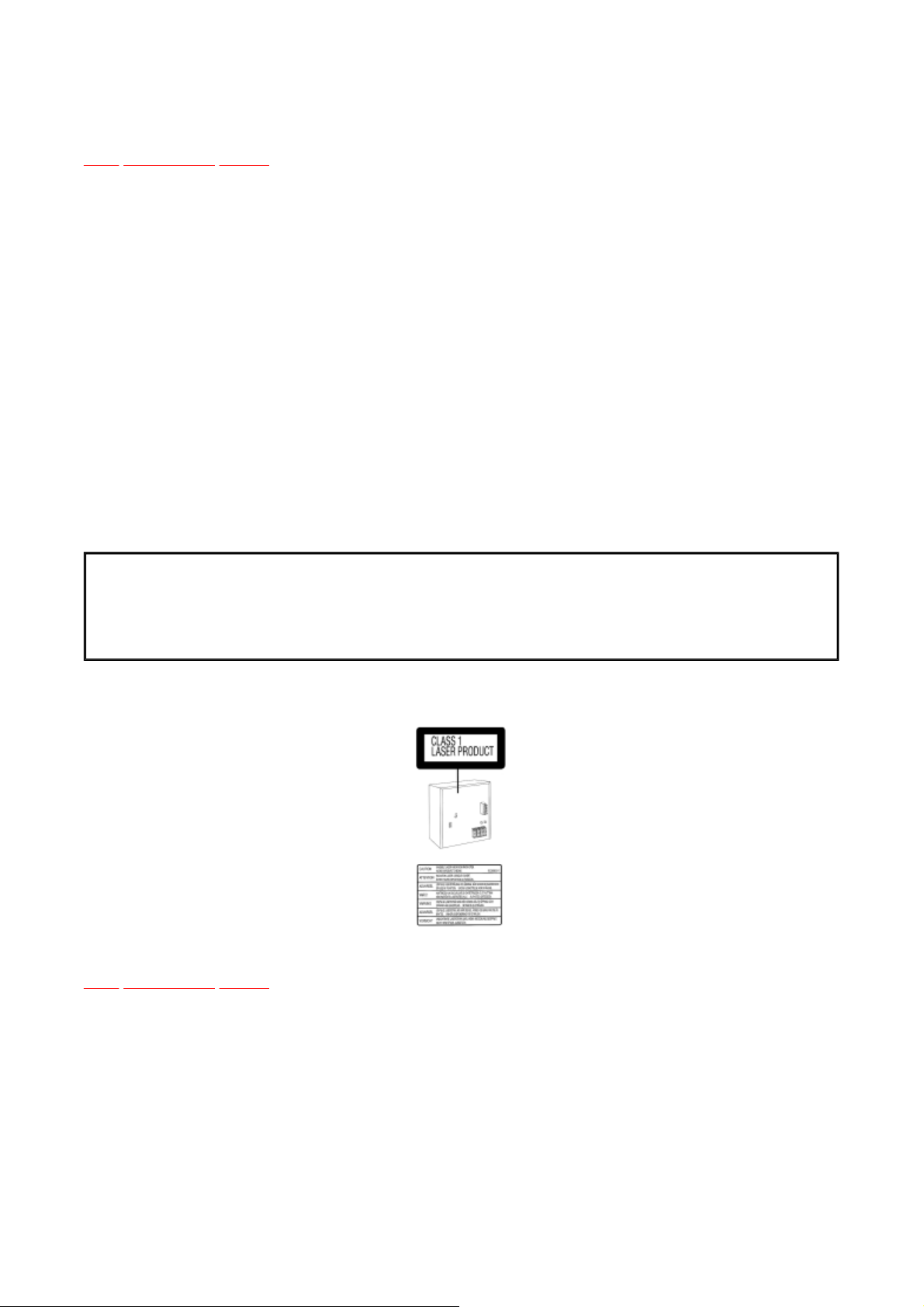
8 Precaution of Laser Diode
TOP PREVIOUS NEXT
This product utilizes a laser diode with the unit turned "ON", invisible laser radiation is emitted from
TOP
PREVIOUS
NEXT
Caution :
the pick up lens.
Wavelength : 780 nm
Maximum output radiation power from pick up : 100 µW/VDE
Laser radiation frompick up unit is safety level, but be sure the followings:
1. Do not disassemble the optical pick up unit, since radiation from exposed laser diode is
dangerous.
2. Do not adjust the variable resistor on the pick up unit. It was already adjusted.
3. Do not look at the focus lens using optical instruments.
4. Recommend not to look at pick up lens for a long time.
CAUTION!
THIS PRODUCT UTILIZES A LASER.
USE OF CONTROLS OR ADJUSTMENTS OR PERFORMANCE OF PROCEDURES OTHER THAN THOSE SPECIFIED HEREIN MAY RESULT IN
HAZARDOUS RADIATION EXPOSURE.
Use of Caution Labels
Page 51

9 Self
-
Diagnostic Function
TOP PREVIOUS NEXT
TOP
PREVIOUS
NEXT
9.1 Self-diagnostic display
9.2 How to enter the Self-Diagnostic Function
9.3 Cassette Mechanism Test (For error code H01, H02, H03, F01, F02)
9.4 CD Mechanism Test (F15, F26, F16, F17, F27, F28, F29, H15)
9.5 To clear all Error code
9.6 How to get out from Self-Diagnostic function
9.7 Power Amplifier Failure (F61)
Page 52

9.1 Self
-
diagnostic display
TOP PREVIOUS NEXT
TOP
PREVIOUS
NEXT
This unit is equipped with a self-diagnostic display function which, if a problem occurs, will display
an error code corresponding to the problem.
Use this function when performing maintenance on the unit.
Page 53

9.2 How to enter the Self
-
Diagnostic Function
TOP PREVIOUS NEXT
TOP
PREVIOUS
NEXT
Page 54

9.3 Cassette Mechanism Test (For error code
H01, H02, H03, F01, F02)
Load a cassette tape with the erasure prevention tab, remove from right side only and close the
TOP
PREVIOUS
NEXT
TOP PREVIOUS NEXT
1. Press “TAPE, DECK 1/2” to select Deck 2.
2. Load a cassette tape with the erasure prevention tab, remove from left side only and close the
cassette holder.
3. Press “FAST FORWARD MEMORY” (Tape will be stop after 2 seconds)
4.
cassette holder.
5. Press “REVERSE FM MODE/BP” (Tape will be stop after 2 seconds)
6. Load a pre-recorded tape with both side record tabs intact and close the cassette holder.
7. Press “PLAY/TUNE/TIME ADJ UP” (After TPS function, tape will stop automatically)
8. Press “REC/STOP” (Tape will not move)
9. Press “STOP/TUNE MODE” to indicate Error code.
If several problem exist, error code will change each time when “ /STOP” is pressed.
(e.g. H01 → H03 → F01 .....etc.)
10. Press “TAPE, DECK 1/2” to select Deck 1.
11. Repeat step 2 to 9 to test Deck 1. (Tape Deck 1 will not check H02 because of no recording
function)
Page 55

9.4 CD Mechanism Test (F15, F26, F16, F17,
F27, F28, F29, H15)
TOP
PREVIOUS
NEXT
TOP PREVIOUS NEXT
1. Press “CD”.
2. Press “OPEN/CLOSE (1)” and place a CD.
3. Press “OPEN/CLOSE (1)” to close the tray.
4. Press “OPEN/CLOSE (5)” and wait until the tray is open.
5. Press “OPEN/CLOSE (1)” and remove the CD.
6. Press “OPEN/CLOSE (1)” to close the tray.
7. Press “/STOP” to indicate Error Code.
If several problem exist, error code will change each time when “/STOP” is pressed.
(e.g. F15 → F26 → F16 ....etc).
Page 56

9.5 To clear all Error code
TOP PREVIOUS NEXT
TOP
PREVIOUS
NEXT
1. Press “STOP/TUNE MODE” button for 5 seconds.
2. FL indicator shows “CLEAR” for 1 second and change to “T”.
Page 57

9.6 How to get out from Self
-
Diagnostic
function
TOP
PREVIOUS
NEXT
TOP PREVIOUS NEXT
1. Press “Power” button OFF.
Page 58

9.7 Power Amplifier Failure (F61)
TOP PREVIOUS NEXT
TOP
PREVIOUS
NEXT
1. When power amplifier fail, F61 will indicate automatically.
Page 59

10 Description of Error Code
TOP PREVIOUS NEXT
TOP
PREVIOUS
NEXT
10.1 Error detection for Cassette Mechanism block
10.2 Error detection for CD Changer block
10.3 Power Supply related error detection
Page 60
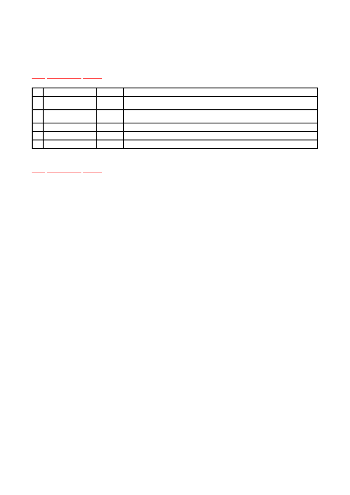
10.1 Error detection for Cassette Mechanism
block
TOP
PREVIOUS
NEXT
TOP PREVIOUS NEXT
NO. Error ErrorDisplay Problem condition
1 MODE SWdetection error H01 Faulty operation of cassette mechanism.Faulty contact or short-circuit of mechanism mode switch (S951,
2 REC INH SWdetection
error
3 HALF SWdetection error H03 Playback cannot perform.Faulty contact or short-circuit of HALF switch (S952, S972).
4 Reel Pulsedetection error H04 The tape advances slightly and then stops.Faulty reel pulse, faulty hole detect IC (IC951, IC971).
5 TPS abnormal F02 Cassette deck will not perform TPS function.Faulty playback EQ/recording amplifier IC (IC1001).
H02 Recording not possible.Faulty contact or short-circuit of REC INH switch (S975).
S971).
Page 61
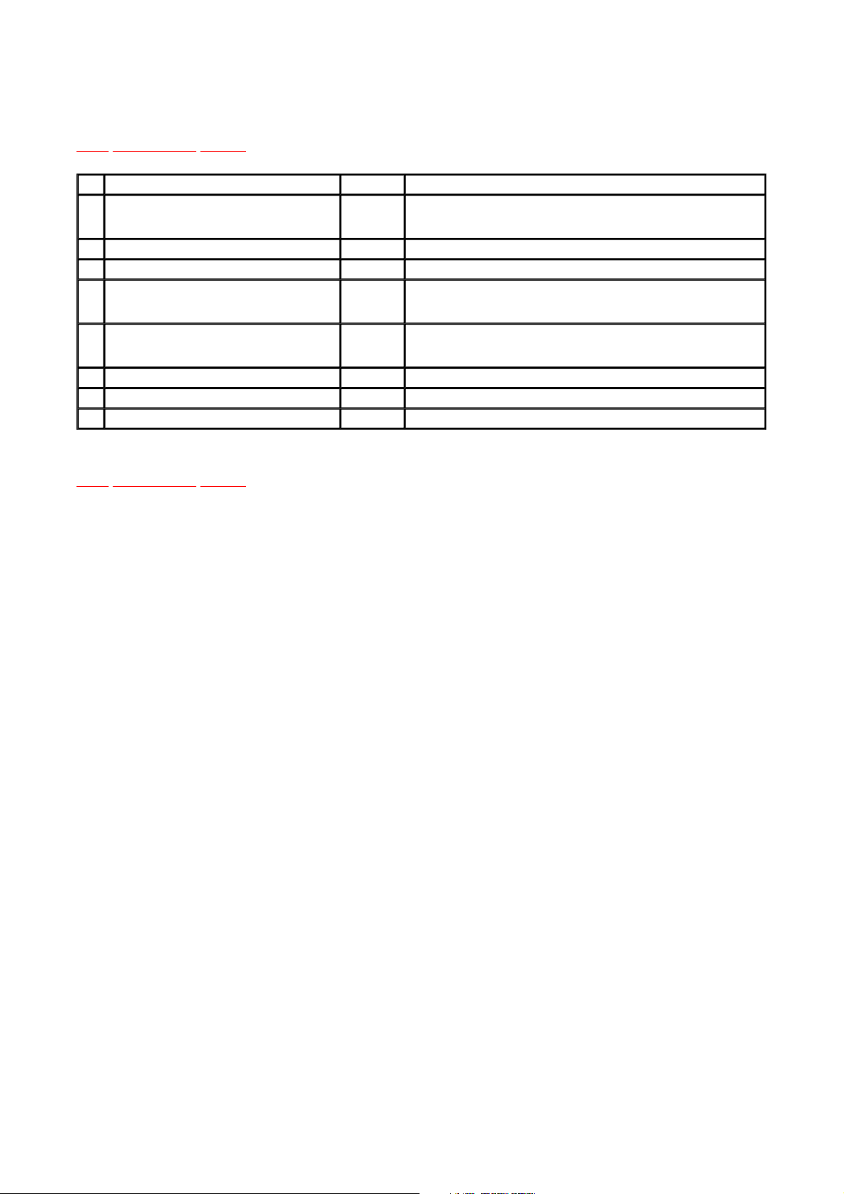
10.2 Error detection for CD Changer block
TOP PREVIOUS NEXT
TOP
PREVIOUS
NEXT
NO. Error ErrorDisplay Problem condition
1 REST SW detection error F15 CD does not function.This error occurs when the Optical Pick Up REST SW
2 CD tray opens automatically F16 CLAMP switch (SW4) NG (Check & Replace)
3 Does not startup when [PLAY]button is pressed F17 BOTTOM switch (SW5) NG (Check & Replace)
4 Transmission error between CDservo LSI and micon
5 Startup fails even when youinsert CD or the selected
disc tray
does not open
6 Cannot insert CD F28 Tray 1 detect switch NG (Check & Replace)
7 Cannot eject CD F29 Check if disc is stuck. Tray 2 detect switch NG (Confirm & Replace)
8 The CD tray closes H15 CD disc tray detect switch NG (SW3) (check & Replace)
F26 CD does not function.This error occurs when the POWER is ON for the CD
F27 Tray 1 detect switch or Tray 2 detect NG (Check & Rplace)
(S701) is not
detected within the specified time (about 8 seconds)
block and an error is
detected after the transmission has started.
Page 62

10.3 Power Supply related error detection
TOP PREVIOUS NEXT
TOP
PREVIOUS
NEXT
NO Error ErrorDisplay Problem condition
1 POWER AMPoutput
abnormal
F61 When POWER is switched on, power become off automatically.During normal operation, if DC DET
become L, PCNT shall become
L and the error display on the left shall be displayed. (IC501)
Page 63

11 CD Test Mode Function
TOP PREVIOUS NEXT
TOP
PREVIOUS
NEXT
This CD test mode is provided to check CD unit without connecting to changer loading mechanism.
This mode shall operate CD PLAY with CD unit being connected only and CD Automatic
Alignment result is shown on FL display.
11.1 How to set CD test mode
11.2 CD Automatically Adjustment result indication
Page 64

11.1 How to set CD test mode
TOP PREVIOUS NEXT
TOP
PREVIOUS
NEXT
Page 65

11.2 CD Automatically Adjustment result
indication
TOP
PREVIOUS
NEXT
TOP PREVIOUS NEXT
Under CD test mode, pressing the numeric key ‘0’ on the remote controller will display the auto
adjustment result. FLOCK, TLOCK and CLVS status shall be shown as below:
During the above display, executing CD PLAY will display auto adjustment result for CD PLAY
mode.
Page 66

12 Measurements and Adjustments
TOP PREVIOUS NEXT
TOP
PREVIOUS
NEXT
12.1 Cassette Deck Section
12.1.1 Tape Speed Adjustment (Deck 1 / 2)
12.1.2 Bias and Erase Voltage Check
12.1.3 Bias Frequency Adjustment (Deck 1 / 2)
12.2 Tuner Section
12.2.1 AM-IF Alignment
12.2.2 AM RF Adjustment
12.3 Alignment Points
12.3.1 Cassette Deck Section
12.3.2 Adjustment Point
Page 67

12.1 Cassette Deck Section
TOP PREVIOUS NEXT
TOP
PREVIOUS
NEXT
Measurement Condition
Make sure head, capstan and press roller are clean.
Judgeable room temperature 20 ± 5 °C (68 ± 9°F)
Measuring instrument
EVM (DC Electronic volmeter)
Digital fruency counter
Test Tape
Tape speed gain adjustment (3 kHz, -10 dB); QZZCWAT
12.1.1 Tape Speed Adjustment (Deck 1 / 2)
12.1.2 Bias and Erase Voltage Check
12.1.3 Bias Frequency Adjustment (Deck 1 / 2)
Page 68
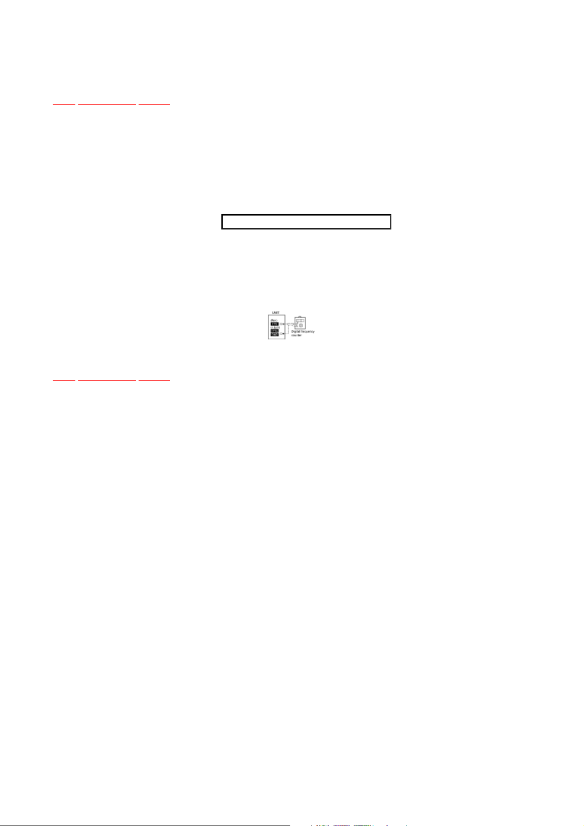
12.1.1 Tape Speed Adjustment (Deck 1/ 2)
TOP PREVIOUS NEXT
TOP
PREVIOUS
NEXT
1. Set the tape edit button to “NORMAL” position.
2. Insert the test tape (QZZCWAT) to DECK 2 and playback (FWD side) the middle portion of
it.
3. Adjust Motor VR (DECK 2) for the output value shown below.
Adjustment target: 2940 ~ 3060 Hz (NORMAL speed)
4. After alignment, assure that the output frequency of the DECK 1 FWD are within ±60 Hz of
the value of the output frequency of DECK 2 FWD.
Fig. 1
Page 69
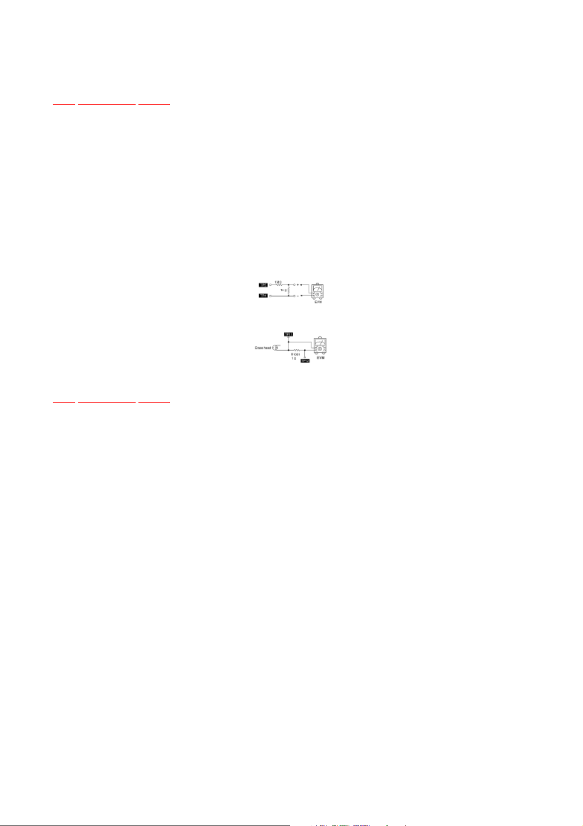
12.1.2 Bias and Erase Voltage Check
TOP PREVIOUS NEXT
TOP
PREVIOUS
NEXT
1. Set the unit “AUX” position.
2. Insert the Normal blank tape (QZZCRA) into DECK 2 and the unit to “REC” mode (use “•
REC/STOP” key).
3. Measure and make sure that the output is within the standard value.
Bias voltage for Deck 2 14±4mV (Normal)
Erase voltage for Deck 2 80mV (Normal)
Fig. 2
Fig. 3
Page 70
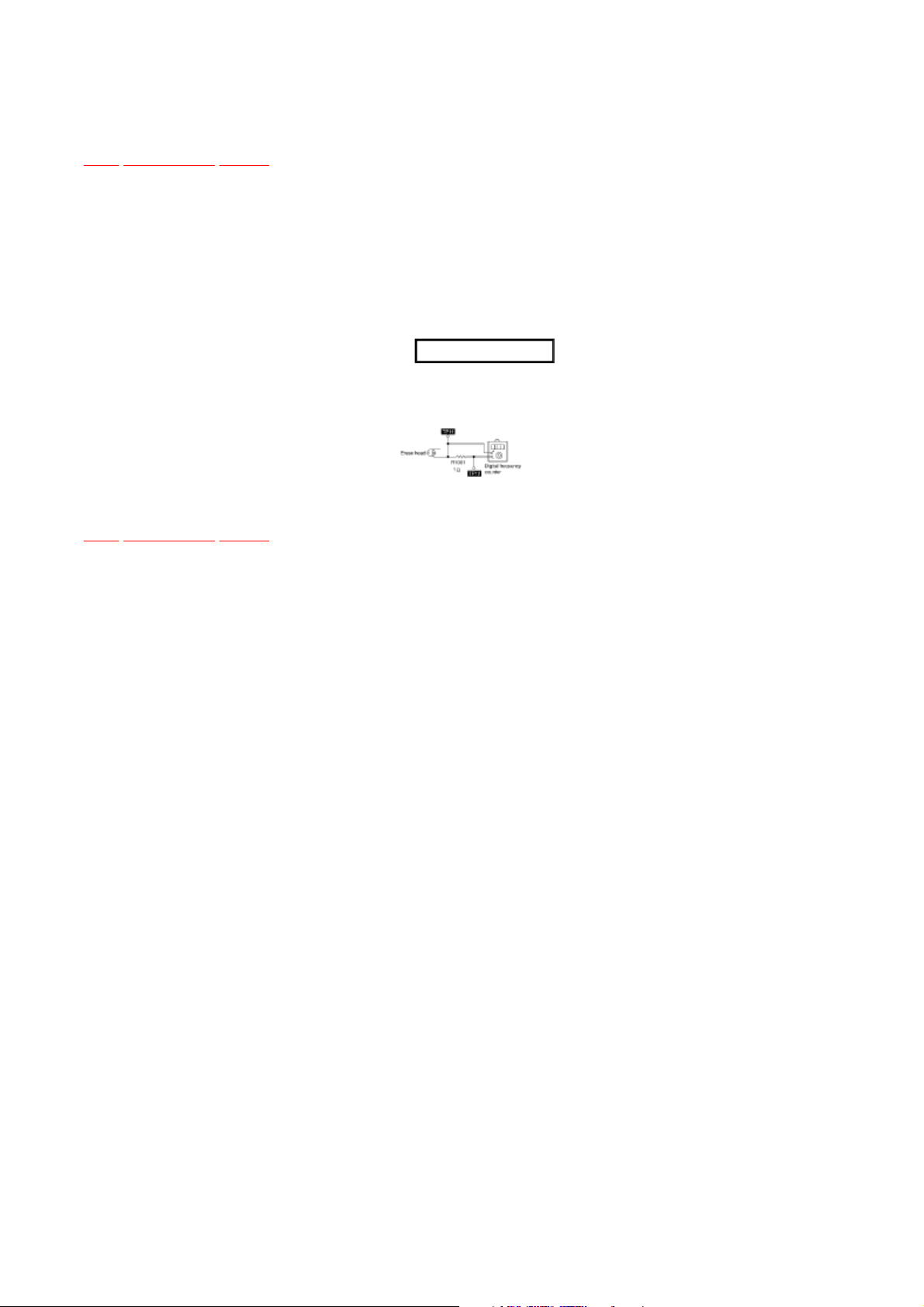
12.1.3 Bias Frequency Adjustment (Deck 1/ 2)
TOP PREVIOUS NEXT
TOP
PREVIOUS
NEXT
1. Set the unit to “AUX” position.
2. Insert the Normal blank tape (QZZCRA) into DECK 2 and set the unit to “REC” mode (• use
“REC/STOP” key).
3. Adjust L1002 so that the output frequency is within the standard value.
Standard Value: 97 ±8 kHz
Fig. 4
Page 71

12.2 Tuner Section
TOP PREVIOUS NEXT
TOP
PREVIOUS
NEXT
12.2.1 AM-IF Alignment
12.2.2 AM RF Adjustment
Page 72
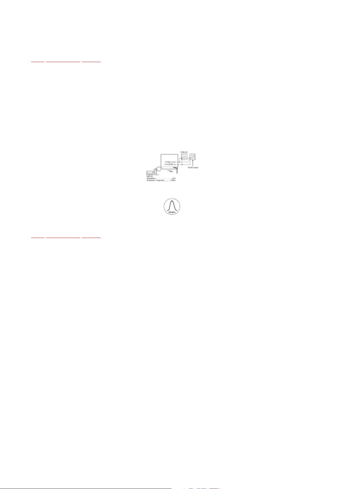
12.2.1 AM
-
IF Alignment
TOP PREVIOUS NEXT
TOP
PREVIOUS
NEXT
1. Connect the instrument as shown in Fig. 5.
2. Set the unit to AM mode.
3. Apply signal as shown in Fig. 5 from AM-SG.
4. Adjust Z102 so that the output frequency is maximized in Fig. 6.
Fig. 5
Fig. 6
Page 73
12.2.2 AM RF Adjustment
TOP PREVIOUS NEXT
TOP
PREVIOUS
NEXT
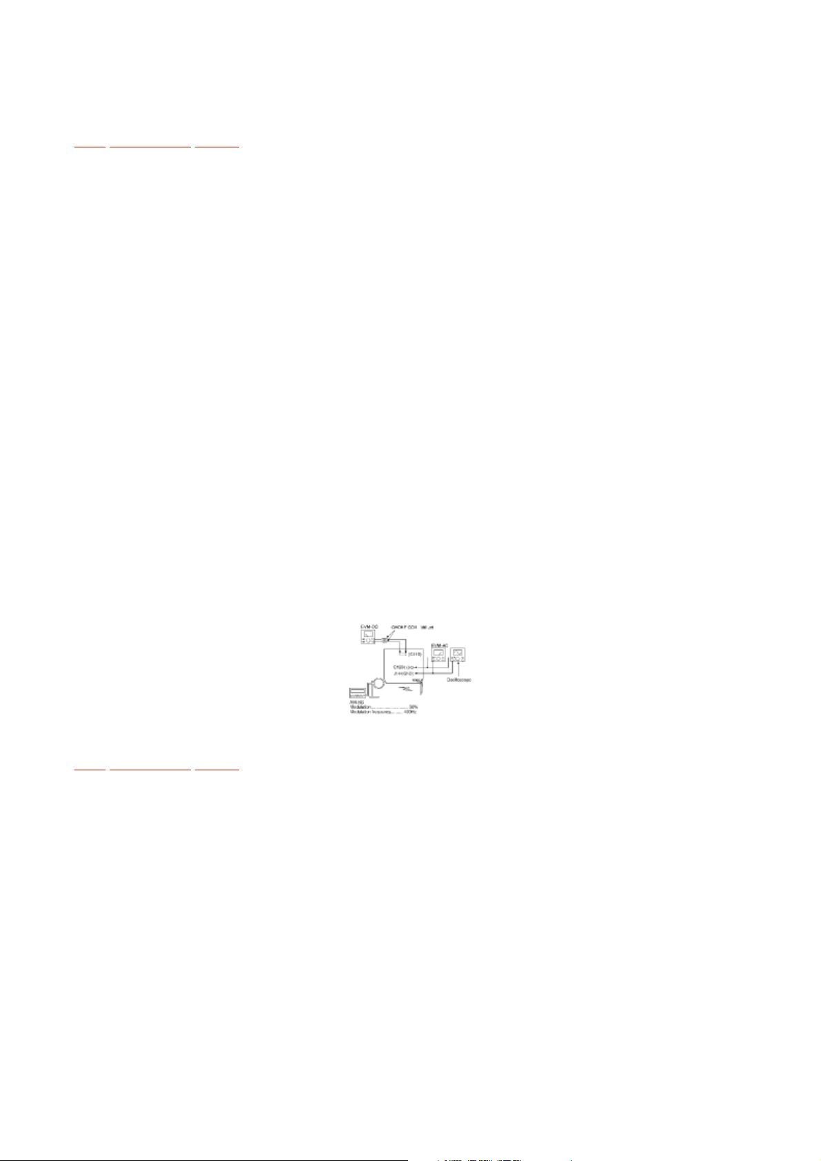
1. Connect the instrument as shown in Fig. 7.
2. Set the unit to AM mode.
3. Set AM-SG to 520kHz.
4. Receive 520kHz in the unit.
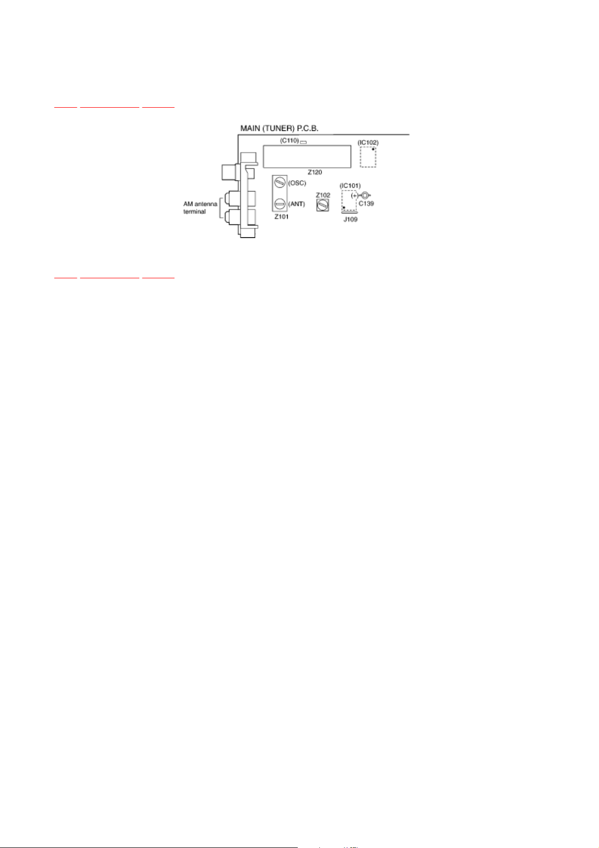
5. Adjust Z101 (OSC) so that the EVM-AC is maximized.
6. Set AM-SG to 600Hz.
7. Receive 600Hz in the unit.
8. Adjust Z101 (ANT) so that the EVM-SG is maximized.
9. Set AM-SG to 520kHz.
10. Receive 520kHz in the unit.
11. Adjust Z101 (OSC) so that the EVM-DC value is with 1.1±0.5V.
Fig. 7
Page 74

12.3 Alignment Points
TOP PREVIOUS NEXT
TOP
PREVIOUS
NEXT
12.3.1 Cassette Deck Section
12.3.2 Adjustment Point
Page 75

12.3.1 Cassette Deck Section
TOP PREVIOUS NEXT
TOP
PREVIOUS
NEXT
Page 76
12.3.2 Adjustment Point
TOP PREVIOUS NEXT
TOP
PREVIOUS
NEXT
Page 77

13 Schematic Diagram
TOP PREVIOUS NEXT
Note:
: Open/ Close switch
(All schematic diagrams may be modified at any time with the development of the new technology)
SW1
: Push switch
SW2
: Push switch
SW3
: Open Switch
SW4
: CD switch
SW5
: Lock switch
S601
: Power switch
S602
: SSEQ switch
S603
: Reset switch
S604
: Deck 1/2 switch
S605
: Rec switch
S606
Page 78

S607
S908
: CD 1 switch
S608
: CD 2 switch
S609
: CD 3 switch
S610
: CD 4 switch
S611
: CD 5 switch
S701
: Reset switch
S901
: REW switch
S902
: Tuner switch
S903
: CD switch
S904
: FF switch
S905
: Stop switch
S906
: Deck 2 switch
S907
: Tape switch
Page 79

: AUX switch
quality sound
IC, LSI and VLSI are sensitive to static electricity.
S909
: Deck 1 switch
S910
: Display switch
S951
: Mode switch
S952
: Half switch
S971
: Mode switch
S972
: Half switch
S975
: Recinh_f switch
VR600
: VR Volume Jog
The voltage value and waveforms are the reference voltage of this unit measured by DC
electronic voltmeter (high impedance) and oscilloscope on the basis of chassis. Accordingly,
there may arise some error in voltage values and waveformsdependingupon the internal
impedance of the tester or the measuring unit.
No mark : Playback << >> : Rec < > : FM
(( )) : CD
Importance safety notice :
Components identified by mark have special characteristics important for safety.
Furthermore, special parts which have purposes of fire-retardant (resistors), high(capacitors), low-noise (resistors), etc. are used. Whenreplacingany of components, be sure to
use only manufacturer´s specified parts shown in the parts list.
Caution !
Page 80

Secondary trouble can be prevented by taking care during repair.
TOP
PREVIOUS
NEXT
Cover the parts boxes made of plastics with aluminium foil.
Put a conductive mat on the work table.
Ground the soldering iron.
Do not touch the pins of IC, LSI or VLSI with fingers directly.
Page 81
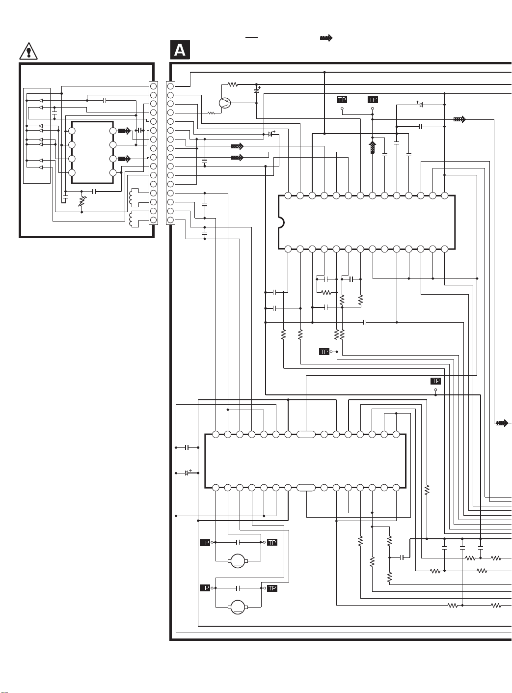
SCHEMATIC DIAGRAM -1
OPTICAL
PICKUP CIRCUIT
LASER DIODE
6
8
11
C
12
10
5
1
4
9
2
2
3
3
4
C
GND
VCC
BIN
AIN
NBOUT
NAOUT
C
GND
VREF
C
8
7
6
5
: +B SIGNAL LINE
: CD-DA SIGNAL LINE
CD SERVO CIRCUIT
R701
Q701
R750
4.7
C713
0.1
C750
0.1
4.7
C701
6.3V33
Q701
B1ADCF000001
LASER POWER DRIVE
C714
6.3V100
1 2 3 4
PDE
FBAL
C712
0.1
C711
0.1
R708
22K
29
52262172081991810171116121513 14
PDF
TBAL
2728
R707
39K
PDA
VCC
FEN
VREF
C747
180P
R744
120K
C749
2200P
R7061KR704
PDB
FEOUT
30
LD
RF
LPD
IC701
AN8885SBE1
SERVO AMP
TEN
TEOUT
NC
23242526
C710
120P
R702
R705
10K
150K
C742
0.027
1K
RFIN
NC
C702
C703
6.3V100
C704
0.1
C706
2700P
C707
0.1
0.027
CEA
BDO
GND
CSBRT
ENV
LDON
OFTR
PDOWN
/RFDET
NC
1
1
VCC
2
2
PDF
3
3
PDE
4
4
LD
5
5
LD GND
6
6
7
8
9
10
11
12
13
14
15
16
CN701
GND
7
NB
8
GND
9
NA
10
VREF
11
LPD
12
GND
13
T-
14
T+
15
F-
16
F+
C751
0.1
C
C735
0.1
C734
10V220
33
28
29
GND
22 23 24
NC
208199181017
D4-
D3-
D3+
D4+
21
NC
PVCC2
PGND2
VCC
VREF
25 26
IN4
27 28161315
NC
IN3
RSTIN
IC703
D1+
NC
D1-
1112
35
30
IN1NCPC2NCIN2
NC
7 12
R735
D2+
D2-
14
36
C737
0.1
GND
PGND1
PVCC1
M
M702
SP MOTOR
38
C736
0.1
37
M
M701
TRV MOTOR
IC703
AN8739SBTE2
FOCUS COIL/
TRACKING COIL/
TRAVERSE MOTOR/
SPINDLE MOTOR DRIVE
/RST
3456
R725
390
100
R724
C715
18K
2700P
R715
1K
R736
100
R727
3.9K
C752
1000P
R723
6.8K
C738
0.01
R729
3.9K
R749
4.7K
C739
1500P
R728
3.9K
R731
6.8K
Page 82
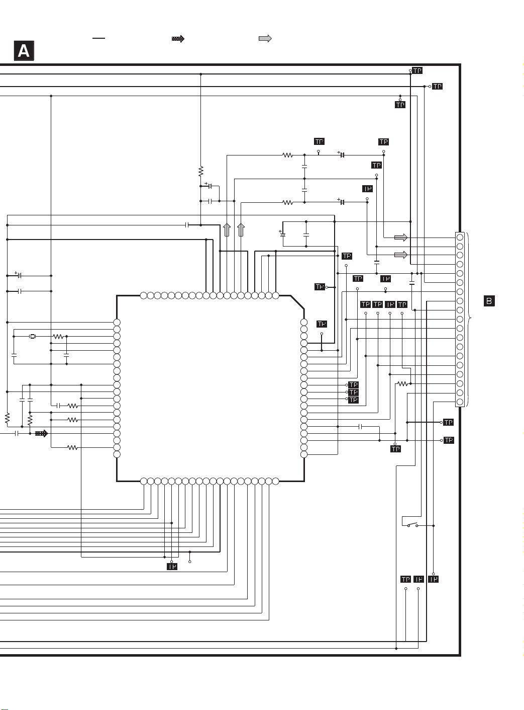
SCHEMATIC DIAGRAM - 2
: +B SIGNAL LINE : CD SIGNAL LINE
CD SERVO CIRCUIT
: CD-DA SIGNAL LINE
20
18
19
C723
10V220
C724
0.1
X701
RSXZ16M9M01T
C722
10P
C717
0.1
R711
82K
C716
820P
C744
5600P
R709
47K
R714
C721
10P
C718
0.22
12
C745
1000P
23
22
21
19
LCH OUT
18
A.GND
17
C753
470P
C743
17
0.1
8
6
7
4
11
10
9
R753
100
5
RCH OUT
+3.3V
D.GND
LD SW
+7.5V
P.GND
MCLK
MDATA
MLD
SPEED
BLKCK
SQCK
SUBQ
STAT
/RST
RESET
SW
TX
2
3
16
15
14
13
12
11
10
9
8
7
6
5
4
3
2
1
CN702
TO
MAIN
CIRCUIT
(CN310) ON
SCHEMATIC
DIAGRAM-5
24
R717
78
IOVDD
79
PSEL
80
MSEL
R718
SSEL
SRDATA
DVDD1
DVSS1
MDATA
SENSE
/FLOCK
/TLOCK
BLKCK
DMUTE
1K
1K
C732
6.3V220
BCLK
LRCK
TX
MCLK
MLD
SQCK
SUBQ
STAT
/RST
SMCK
CSEL
1
2
3
4
5
6
7
8
9
10
11
12
13
14
15
16
17
18
19
20
R721
100
C731
6.3V220
C730
0.1
C754
470P
72
69
71
70
RESY
/TEST
IOSEL
IC702
DIGITAL FILTER/
73
AVDD1
74
OUTL
75
AVSS1
76
OUTR
77
RSEL
62
63
61
FCLK
BYTCK
60
VDD
59
X2 OUT
58
X1 IN
VSS
0
R712
220
R741
47K
R742
220K
57
56
55
54
53
52
51
50
49
48
47
46
45
44
43
42
41
SBCK
SUBC
VCOF2
PCK
EFM
AVSS2
AVDD2
VCOF
PLLF
DSLF
DRF
IREF
ARF
WVEL
DSLF2
PLLF2
/CLDCK
68
66
64
65
67
CRC
CLVS
FLAG
IPFLAG
DEMPH
MN662790RSC
SERVO PROCESSOR
DIGITAL SIGNAL PROCESSOR/
D/A CONVERTER
C725
1000P
C726
1000P
C733
0.1
C727
50V1
C728
50V1
27
25
26
40
LDON
39
BDO
/RFDET
38
37
42
OFT
TRCRS
36
VDET
32
33
30
34
31
35
TJ701
KICK
28
29
25
26
27
TRV
22
21
24
23
S701
RESET SW
1
15
16
TVD
PC
ECM
ECS
TRD
FOD
VREF
FBAL
TBAL
FETERFENV
Page 83
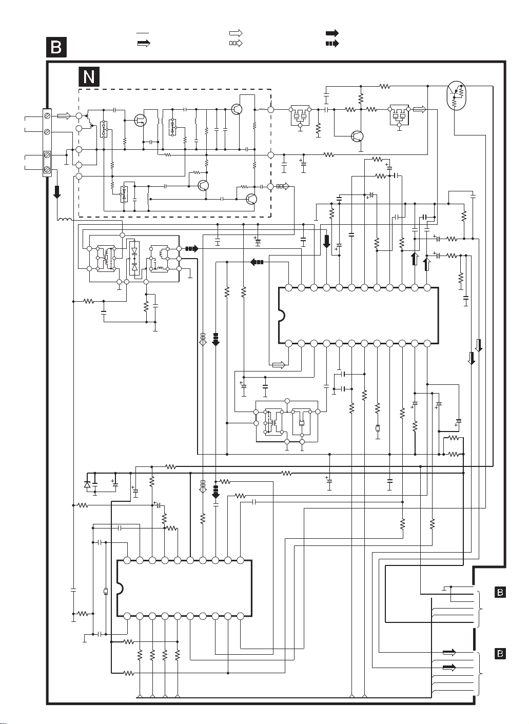
SCHEMATIC DIAGRAM - 3
: +B SIGNAL LINE
: FM/AM SIGNAL LINE
TUNER/MAIN CIRCUIT
: FM SIGNAL LINE
: FM OSC SIGNAL LINE
: AM SIGNAL LINE
: AM OSC SIGNAL LINE
FM EXT
ANT
75 OHM
GND
AM LOOP ANT
AM EXT
ANT
JK101
1
2
3
4
1
2
3
4
5
L102
RLQB1R0KTD-D
R110
1K
D101
UDZSTE175R1B
R114
5.6K
TUNER PACK Z120
AM ANT COIL
2
1
Z101
RLA2Z007-T
C107
0.047
C132
1000P
C133
27P
2SK544F-AC
RF AMP
5.6P
D
G
S
100K
100K
2.7K
3
8
9
R112
100K
LA1833NMNTLM
FM/AM IF AMP
DET/AM OSC MIX/
C125
C130
6.3V100
16V22
C112
0.01
1000P
3.3P
AM OSC COIL
7
IC101
FM MPX
R113
10K
C111
50V4.7
4.7P
C108
8P
220
R111
R116
390
R115
560
1K
Q106
C116
50V4.7
AM OUT
SD
R126
0.033
1K
R104
1K
R107
330
J0B1075A0061
1
R101
0
Q101
2SC2058SPTA
FM IF AMP
R121
22K
C138
R143
22K
C139
50V4.7
C131
150P
4.7K
R102
16101511141213
PILOT IN
DET OUT
ST
FM DET
470
R125
33
R124
X102
RLFDFT22DD
C149
0.1
CF202
2
Q101
C120
16V10
0.01
MPX IN
VCC
3
3300P
0.01
C118
68K
R123
RCH
IC101
PILOT OUT
FM/AM
STRQ
470
R127
R132
10K
C137
C122
R122
LCH
MONO
50V1
2.7K
C117
0.01
Q106
KRA102MTA
TUNER 15V
SUPPLY SWITCH
C144
4700
R146
100K
R142
6.8K
C142
R141
50V1
6.8K
C141
50V1
R145
100K
C143
4700
C121
50V4.7...GC
50V0.47...GN
R144
120
R131
120
R133
1K
C123
50V1
3
2
C102
16V10
2324
OSC
AM MIX OUT
C106
6
0.01
AFC
REG
4
C104
1000P
R105
R120
47K
470
R103
270
C119
680P
2122
AM RF IN
AM IF IN
C103
0.01
6.3V100
R106
470K
C115
AGC
GND
5206197188179
C147
1000P
C148
0.01
C129
B1AAAC000011
100K
1.2u
180P
560K
FM MIXER
3.3P
18P
680K
390
B1AAAD000013
BUFFER AMP
LOCAL OSC
2.2P
C136
1000P
R117
47K
C113
1000P
82
R151
R119
3.3K
R129
27K
1000P
680K
0.47u
390
390
R118
3.3K
C127
16V22
2
1
RLI2Z021M-T
C124
100P
5.6P
50V3.3
2.2P
4
5
6
7
6
8
C114
C126
Z102
J0B1075A0061
1
C101
0.01
C109
1000P
OSC OUT
FM IF IN
1 2 3 4
1
3
5
R128
82
CF201
C110
0.01
R152
17181920
PD
AIN
VSS
XOUT
H0H720400005
X103
0
C134
27P
AOUT
LC72131MDTRM
PLL FREQUENCY SYNTHESIZER
CEDICL
XIN
1 2 3 4
R138
3.3K
R130
10K
1K
R137
CE
1K
R136
PLLDA
VDD
FMIN
IC102
LW
AM
DO
51661571481391210
470
1K
R134
R135
DO/ST
PLLCLK
AMIN
SDC
MONO
STRQ
11
IFIN
TGND
TO
15V
DO/ST
+7.5V
RCH
LCH
PLLDA
DO/ST
PLLCLK
SD
CE
MAIN
CIRCUIT
(2A) ON
SCHEMATIC
DIAGRAM-6
1A
TO
MAIN
CIRCUIT
(2B) ON
SCHEMATIC
DIAGRAM-6
1B
FM
DO/ST
SD
DET_OUT
Page 84
TO
DECK
CIRCUIT
(CN1001) ON
SCHEMATIC
DIAGRAM-11
AUX
TO
CD LOADING
CIRCUIT
(CN1) ON
SCHEMATIC
DIAGRAM-13
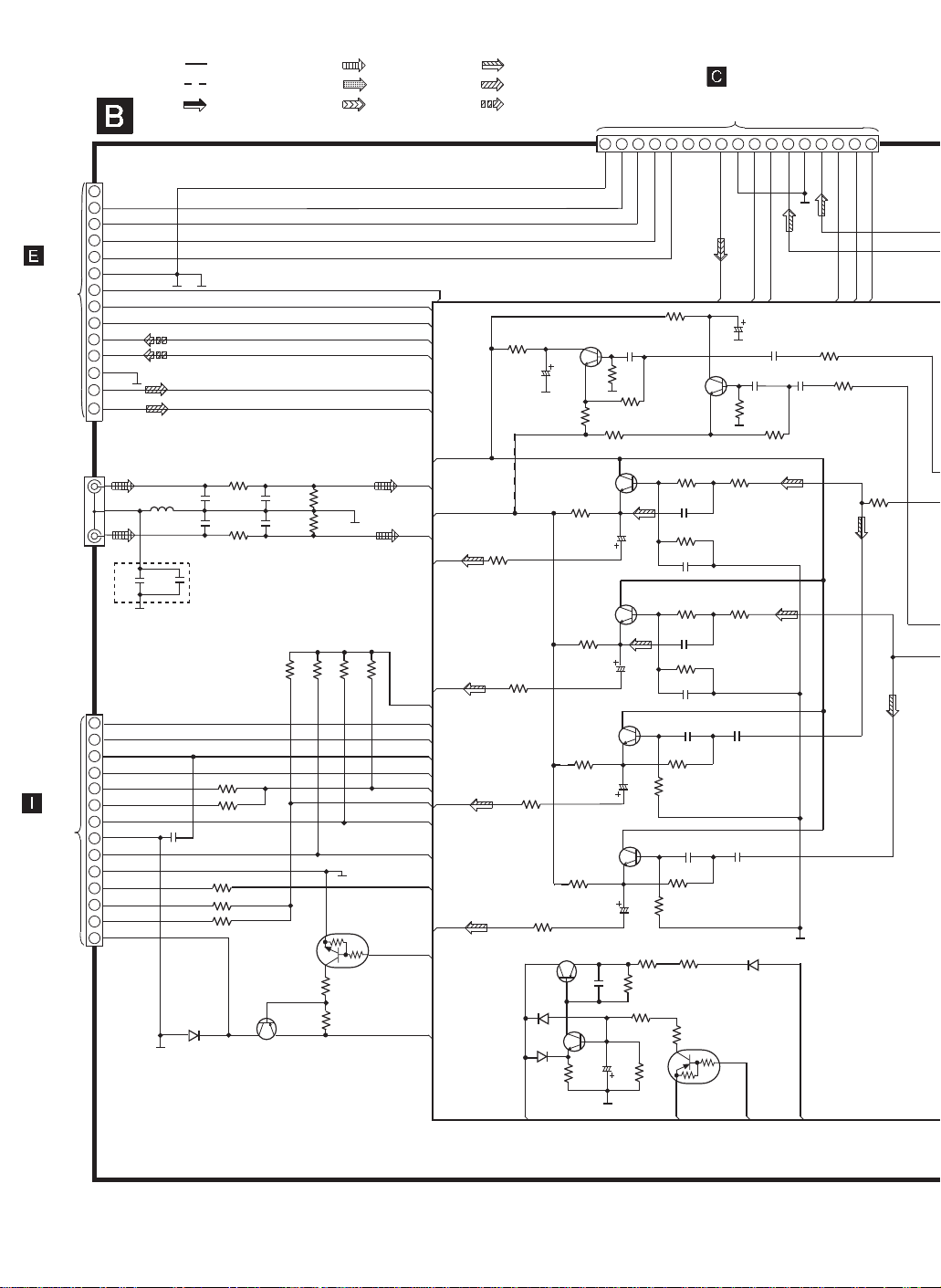
SCHEMATIC DIAGRAM - 4
: +B SIGNAL LINE
: -B SIGNAL LINE
: FM/AM SIGNAL LINE
MAIN CIRCUIT
CR02
1
MOTOR
2
BP1
3
DECK1_H
4
DMT
5
P_GND
6
MOT10V
7
REC_H
8
+15V
9
REC_R
10
REC_L
11
AGND
12
PBR
13
PBL
14
CN304
R201
RCH
LCH
JK300
CN309
CHG_CW
14
CHG_HALF
13
8V
12
CHG_CCW
11
CLAMP
10
OPEN
9
SW1
8
PGND
7
SW2
6
DGND
5
5V
4
POSITION
3
BOTTOMSW
2
PLUNGER
1
L301
J0JBC0000019
FOR GC ONLY
0.22
C331
0.22
C332
C326
0.47
RL1N4003N02
10K
680P
C201
680P
C401
R401
10K
22K
R344
12K
R345
220
R348
R346
22K
12K
R347
D324
Q324
KTA12710YTA
CD MOTOR SUPPLY SWITCH
Q324
3.3K
100P
C202
R202
3.3K
100P
C402
R402
47K
10K
R341
R340
R342
Q323
1K
R349
10K
R350
KRC102STA
PLUNGER MOTOR
SUPPLY CONTROL SWITCH
: AUX SIGNAL LINE
: CD SIGNAL LINE
: MIC SIGNAL LINE
47K
10K
R343
CHG_HALF
CHG_CCW
CHG_AD1
CHG_AD2
CHG_PLGR
Q323
MOT10V
REC_H
+15V
REC_R
REC_L
PBR
PBL
AUXR
AUXL
VREF+
CHG_CW
CD8V
SW1
SW2
SW5V
MOT10V
+9.0V
-9.0V
LO_L
LO_R
HI_L
HI_R
: MAIN SIGNAL LINE
: PLAYBACK SIGNAL LINE
: RECORD SIGNAL LINE
R352
220
C318
16V33
+9.0V
-9.0V
R443
2.7K
R243
2.7K
R444
1.8K
R244
1.8K
Q308
D307
D307-D308
MA2J72800L
D308
CD3.3V
17 16 15 14 13 12 11 10
MOTOR
PL_GND
C451
Q411
0.033
220k
R472
R473
R271
12K
R471
12K
Q404
R439
10K
C435
50V0.68
Q204
R239
10K
50V1
C235
Q405
R442
10K
50V1
C434
Q205
R242
10K
50V1
C234
0.01
10K
C316
R313
Q309
C315
330
10V33
R317
220
R316
BP1
R315
2.2K
3.9K
TO
PANEL CIRCUIT
(CP601) ON
SCHEMATIC DIAGRAM-9
+9V
DMT
DECK1_H
RDS_DET
R353
220
Q211
R437
18K
C430
0.015
R438
220K
C431
820
R237
18K
C230
0.015
R238
220K
C231
820
C433
8200P
R440
4.7K
KTC3875GRTA
12K
R441
C233
8200P
R240
4.7K
12K
R241
R312
R311
12
15
100
R314
Q310
SW5V
MIC
REC_H
SPEANA
MIC GND
MIC
SPEA
REC_H
C319
C452
16V33
0.033
C251
0.033
220K
R272
R273
220
R436
18K
Q204, Q404
KTC3875GRTA
LPF FREQ AMP
SWITCH
R236
18K
C432
8200P
Q205, Q405
HPF FREQ AMP
SWITCH
C232
8200P
D309
RL1N44003N02
/CD
HPL
HPR
HPGND
MUTE_A
MUTE_A
R474
1.5K
C252
R274
0.033
1.5K
KTC3875GRTA
RHP FILTER
(HEADPHONE)
KTC3875GRTA
LHP FILTER
(HEADPHONE)
KTA12710YTA
CURRENT CONTROL
KTC3199GRTA
VOLTAGE STABILISER
KRA110MTA
SUPPLY SWITCH
CD8V
24689 7 5 3 1
MUTE_H
MUTE_H
Q211
Q411
Q308
SWITCH
Q309
CD3.3V
Q310
CD ON/OFF
/CD
/CD
LHPF
RHPF
R454
220
CN303
Page 85
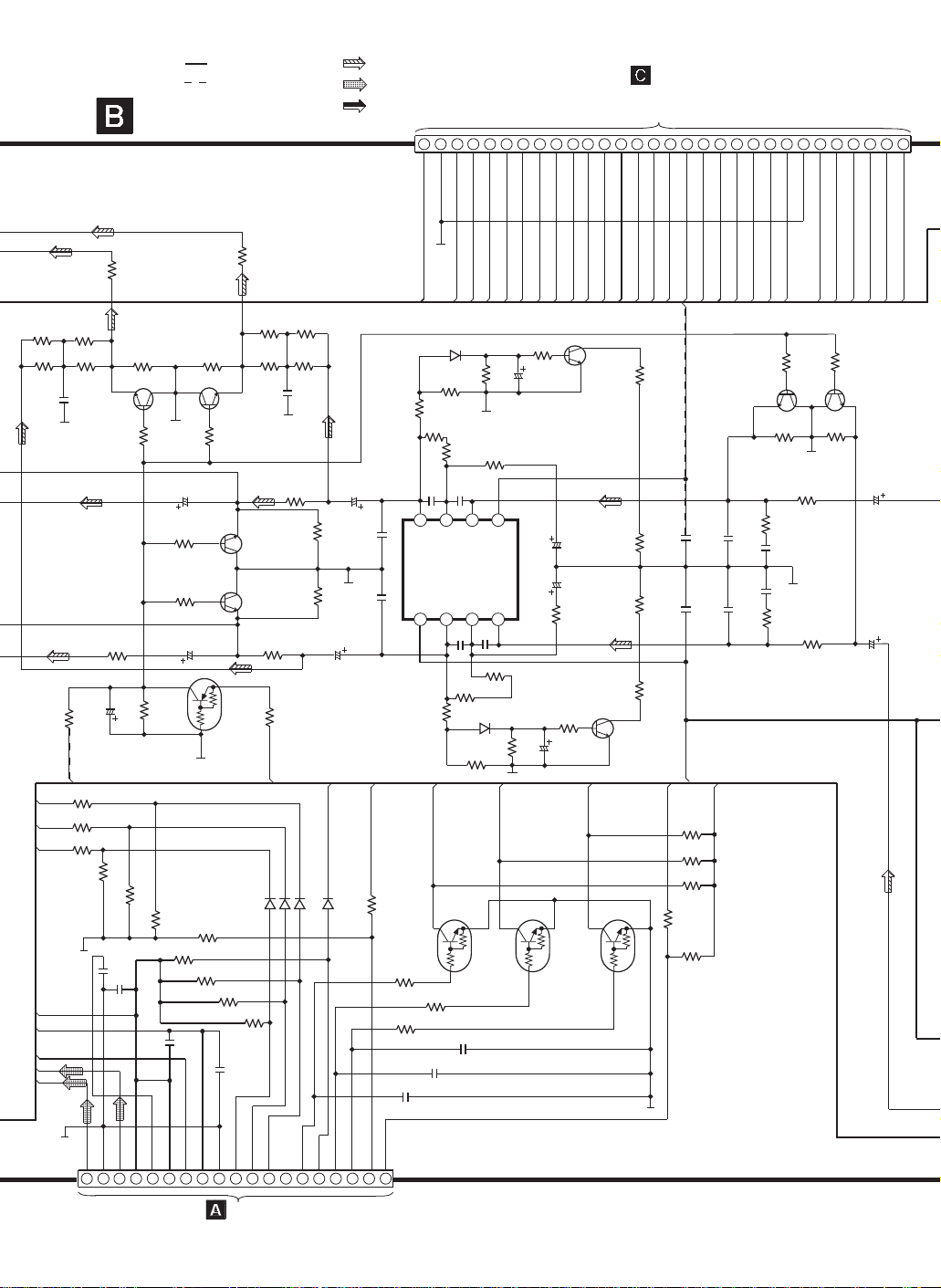
SCHEMATIC DIAGRAM - 5
MAIN CIRCUIT
1
R203
Q203, Q403
R206
33
R207
33
C203
1000P
KTD1304TA
MUTING SWITCH
R204
33
R205
33
Q202, Q402
KTD1304TA
HEADPHONE MUTING
SWITCH
R208
3.3K
Q203 Q403
1.5K
R209
R254
220
C429
50V1
R435
1.5K
R235
1.5K
C229
50V1
: +B SIGNAL LINE
: -B SIGNAL LINE
1
R403
R408
3.3K
1.5K
R409
Q402
Q202
R404
R405
33
R228
33
2.2K
C403
1000P
R428
2.2K
R406
33
R407
33
R434
R234
100K
100K
: MAIN SIGNAL LINE
: CD SIGNAL LINE
: FM/AM SIGNAL LINE
C427
16V10
C440
1000P
C240
1000P
C227
16V10
TO
PANEL CIRCUIT
(CP602) ON
SCHEMATIC DIAGRAM-9
30 29 28 27 26 25 24 23 22 21 20 19 18 17 16 15 14 13 12 11 10
SW2
CHG_AD1
CHG_AD2
CHG_AD1
CHG_AD2
R431
C425
100P
+IN1
/RESTSW
/RESTSW
100K
R426
3.3K
GNDOUT1
SW1
CHG_PLGR
SW2
SW1
CHG_PLGR
R430
1K
C428
16V10
KTC3875GRTA
C424
CHG_CW
CHG_CCW
CHG_HALF
CHG_CCW
CHG_CW
CHG_HALF
Q401
Q401
AGC CONTROL
50V4.7
VREF+
DC_DET
DC_DET
VREF+
R429
R425
MDATA/PLLDA
PLLDA
12K
47K
ASP_DAT
ASP_CLK
ASP_DAT
ASP_CLK
C313
BLKCLK
BLKCLK
-9.0V
0.01
MCLK/PLLCLK
PLLCLK
AGND
MOT10V
MOT10V
D401
MA2J72800L
R433
4.7K
2.2K
R432
R460
0
47K
R427
C426
47
1 2 3 4
-IN1
IC301
50V1
VCC
OUT2
C226
47
-IN2 +IN2
C225
100P
C224
5678
3.3K
R226
R225
47K
C312
0.01
LED9V
LED9V
C423
C223
4700
4700
SUBQ
ST/D0/SQCK
SUBQ
ST/D0/SQCK
Q407
R424
C422
C222
R224
4.7K
0.047
0.1
4.7K
/CDRST
STATUS
/CDRST
1.5K
R456
R455
100K
STATUS
D.GND
R423
2.7K
R223
2.7K
PLLCE1
PLLCE1
1.5K
R256
R255
100K
SD
SD
24689 7 5 3 1
LM_R
SW5V
MLD/PLLCE
LM_L
LM_R
SW5V
PLLCE
Q207, Q407
KTD1304TA
MUTING SWITCH
Q207
C421
16V10
C221
16V10
CN302
LM_L
R310
C309
27K
50V4.7
R309
KRA102STA
AUDIO MUTING
CONTROL SWITCH
-9.0V
R324
100
PLLCE
R322
100
PLLDA
R320
100
PLLCLK
100K
R321
100K
R323
C320
1000P
C321
CD3.3V
CD7.5V
TX
CDR
CDL
1000P
CDAGND
CD3.3V
LCH OUT
RCH OUT
19 18 17 16 15 14 13 12 11 10
56K
Q301
R327
100K
R325
10K
R328
5.6K
R329
5.6K
C317
1000P
CDDGND
+7.5V
TX
LD_SW
TO
SERVO CIRCUIT
(CN702) ON
SCHEMATIC DIAGRAM-2
Q301
R330
5.6K
PGND
C322
MCLK
R331
5.6K
1000P
MDATA
R318
2.2K
MUTEA
MLD
MA2J72800L
D320
SPEED
IC301
C0AABB000117
HEADPHONE AMP
Q201
KTC3875GRTA
AGC CONTROL
ST/DO/SQCK
MA2J72800L
MA2J72800L
MA2J72800L
R326
D322
D323
D321
STAT
SUBQ
SQCK
BLKCK
4.7K
RST
24689 7 5 3 1
/CDRST
R339
4.7K
R337
4.7K
C323
100P
/REST SW
CN310
R338
4.7K
C324
100P
R232
R260
2.2K
BLKCLK
C325
100P
R227
0
47K
D201
MA2J72800L
R233
4.7K
R231
100K
SUBQ
12K
STATUS
Q322
R229
Q201
+9.0V
SW5V
R334
/RESTSW
10K
R335
10K
R336
10K
1K
R332
R333
10K
Q321
KRC101STA
SUBQ INTERFACE SWITCH
Q320
KRC101STA
BLKCLK INTERFACE SWITCH
Q322
KRC101STA
CD STATUS INTERFACE SWITCH
R230
1K
C228
16V10
Q321Q320
Page 86
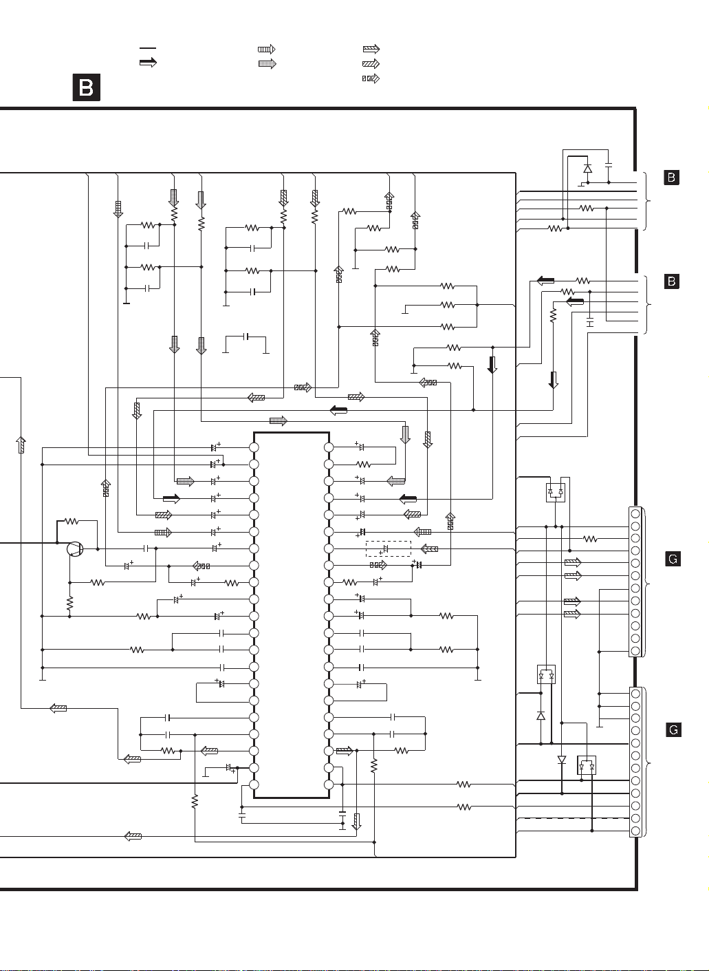
SCHEMATIC DIAGRAM - 6
MAIN CIRCUIT
REF
AUXL
R357
22K
Q302
R355
4.7K
Q302
KTC3875GRTA
VOLTAGE REGULATOR
C330
C412
R356
100
AUDIO SOUND PROCESSOR
16V10
R419
1.5K
R420
3.9K
IC300
C1BB00000747
: +B SIGNAL LINE
: FM/AM SIGNAL LINE
CDL
R411
82
5.6K
R410
C413
C411
0.47
0.47
R210
50V0.47...GC
47 K
R421
C404
220P
R211
5.6K
C204
220P
0.039
C419
C420
R422 820
CDR
82
6.3V100
C310
C311
6.3V100
C406 16V10
16V10
C407
16V10
C408
C409
16V10
16V10
C306
R458
0
16V10
C414
50V0.47
C415 0.15
0.15
C416
C417 1500P
C418
16V10
C305
10V220
C308
R415
C303
1000P
100P
47K
C405
220P
R215
47K
C205
220P
1
REF IN
2
REF OUT
3
IN A1
4
IN B1
5
1N C1
6
IN D1
VCUT
7
8
REC1
9
10
TBO1
11
12
13
TMO1
14
TT1
15
TOUT1
16
B_VOLIN1
17
BB_A1
BB_B1
18
OUT1
19
VCC
20
DATA
21
R414
A_VOLIN1
TBI1
TMI1
: AUX SIGNAL LINE
: CD SIGNAL LINE
PBL
PBR
R416
100K
1K
1K
R214
C304
42
SUR1
R305
SUR2
41
C206
40
IN A2
C207
39
IN B2
38
IN C2
37
IN D2
36
MIC IN
35
REC2
TBI2
TBO2
TMI2
TMO2
TT2
TOUT2
BB_A2
BB_B2
OUT2
GND
CLOCK
R258
34
C213
33
C214
32
31
30
29
C218
28
27
26
25
24
23
22
100P
C307
A_VOLIN2
IC300
BVOLIN2
: MAIN SIGNAL LINE
: PLAYBACK SIGNAL LINE
: RECORD SIGNAL LINE
REC_L
R417
8.2K
R217
8.2K
R216
100K
50V1
6.8K
16V10
16V10
16V10
C208
C209
16V10
FOR GC ONLY
C329
16V10
0
16V10
C211
50V0.47
50V0.47
0.15
C215
0.15C216
C217 1500P
16V10
C219
C220
R222
47K
R221
REF
C212
0.47
0.47
820
REC_R
16V10
R218
56K
R304
R418
R219
1.5K
R220
3.9K
10K
56K
R213
47K
R413
47K
R307
2.2K
R308
2.2K
SPEA
AUXR
ASP_CLK
ASP_DAT
MIC
15V
DET_OUT
ST/DO/SQCK
SD
+9V
PLLCE1
PLLDA
PLLCLK
+9V
DC_DET
MUTEH
+15V
HI_L
HI_R
LO_L
LO_R
D303
CD7.5V
D306
CD8V
D302
LED9V
MOT10V
+9V
-9V
SW5V
D301
UDZSTE177R5B
D301
R303
27
R212
R301 4.7K
1K
R412
D304
D302
B0ACCK000005
D303-D305
DAP202KT146
D306
RL1N4003N02
R302
10K
1K
C301
R319
1000P
2.2K
D305
0.01
C302
DET_OUT
DO/ST
DO/ST
PLLCLK
FAN
DC_DET
MUTE_H
+15V
HIGH_LIN
HIGH_RIN
A_GND
LOW_LIN
LOW_RIN
SURR
SUBW
T GND
P GND
D GND
uP GND
CD8V
FAN
LED9V
MOT10V
+9V
SW5V
TGND
15V
SD
+7.5V
RCH
CE
LCH
PLLDA
-9V
TO
TUNER
CIRCUIT
(1A) ON
SCHEMATIC
DIAGRAM-3
2A
TO
TUNER
CIRCUIT
(1B) ON
SCHEMATIC
DIAGRAM-3
2B
1
2
3
4
5
TO
POWER
6
CIRCUIT
(CN500) ON
7
SCHEMATIC
8
DIAGRAM-12
9
10
11
12
CN300
1
2
3
4
5
6
7
8
9
10
11
12
CN301
TO
POWER
CIRCUIT
(CN501) ON
SCHEMATIC
DIAGRAM-12
Page 87
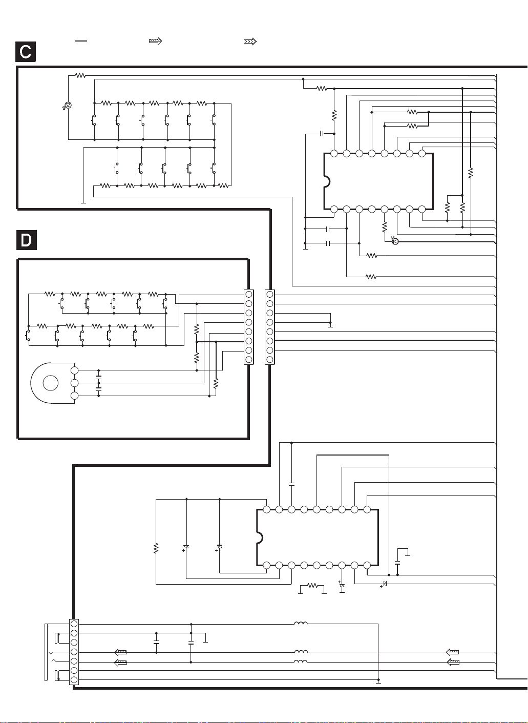
SCHEMATIC DIAGRAM - 7
: +B SIGNAL LINE
PANEL CIRCUIT
R600
4.7K...GC
D600
B3AAA0000583
POWER
R601
S601
R611
68K
R602
1K
1K
S602
SSEQ
CD5
S611
R610
22K
TACT SWITCH CIRCUIT
R905
2.2K
STOP
R906
2.7K
S906
TAPE
DECK2
VR600
EVEKE2F3524B
JOG VOL
S907
S905
R907
4.7K
R904
1.8K
3
2
COM BA
1
AUX
FF
S908
S904
R908
6.8K
R903
1.2K
DECK1
C901
100P
C902
100P
R902
1K
CD
S903
R909
10K
S909
DISPLAY
R603
S603
PRESET EQ
CD4
S610
R609
10K
R901
S902
TUNER
R910
22K
S910
1.2K
1K
: MAIN SIGNAL LINE
R604
R605
1.8K
2.2K
REC
S604
S609
R608
6.8K
S901
CD2
R900
R912
10K
S605
47K
S608
R607
4.7K
DECK 1/2
CD3
REW
S606S607
OPEN/CLOSE
CD1
R606
2.7K
MICSW_1
VJOG_B
VREF+
VJOG_A
R913
47K
K2_1
8
7
6
5
4
3
2
1
: MIC SIGNAL LINE
IC601
C1BB00000574
I/O EXPANDER
CN900
MICSW
8
K2
7
6
5
VJOG_B
4
VREF+
3
VJOG_A
2
1
CP900
R681
10K
C636
0.1
C634
100P
C635
100P
100
R612
2PL
1PL
VCC
DAT
CLK
GND
1 2 3 4
R613
13141516
H1
IC601
NC
5126117108
1.2K
R687
R614
1K
B3AAA0000583
1K
BP1
REC
DMT
SSEQLED
D609
R623
4.7K
R622
4.7K
1M
MUTE_A
9
/CD
MUTE_H
R619
4.7K
R618
4.7K
SYS6V
VREF+
PL2
PL1
H_DECK1
SW5V
REC_H
BP1
MOTOR
4.7K
R617
MUTEH
MUTEA
DMT
LED9V
SER4
SER3
HP_SW
MICSW
VJOG_B
VREF+
VJOG_A
K1
/CD
K2
HEADPHONE
JK601
LM_R/SPE
SP_C
IC603
C1BB00000086
SPECTRUM ANALYSER
GND
C656
AOUT
0.01
TEST
15161718
NC
NC
SEL
10
B
C
SP_B
SP_A
IC603
C660
100K
R680
1
7
6
3
2
5
4
C621
0.022
C620
0.022
50V0.1
C661
50V0.1
BIASC
1
L602-L604
G0C101KA0029
VREFC
2
RREFC
3 4
L604
L603
L602
NC
R675
4.7K
NC
DIFOUT
CIN
C659
AIN
50V0.1
5146137128119
VCC A
C658
50V0.1
C657
0.01
DVREF+
SPEA
HPR
HPL
HP_SW
Page 88
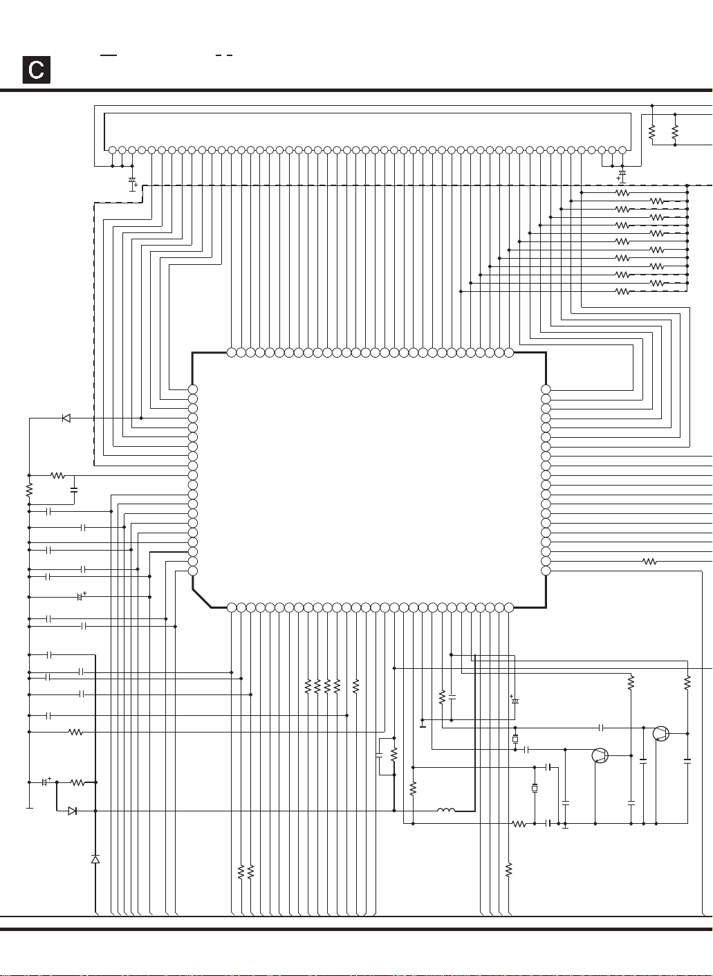
SCHEMATIC DIAGRAM - 8
: +B SIGNAL LINE
PANEL CIRCUIT
: -B SIGNAL LINE
B0AACK000004
R626
R627
1K
22K
C648
560P
C646
560P
C602
0.01
C649
560P
C651
1000P
C653
560P
C655
560P
C600
10V1000P
MA2C72300F
D605
R632
D610
FL600
A2BD00000061
1 2 3 4 5 6 7 8 9 10 11 12 13 14 15 16 17 18 19 20 21 22 23 24 25 26 27 28 29 303132 33 34 35 36 37 38 39 40 41 42 43 44 45 46 47 48 49 50 51 52 53
C641
35V22
79
80
76
77
10V22
10K
R630
680
C603
330P
C647
560P
C645
560P
C601
C650
560P
C652
560P
C654
560P
1SS380TE-17
D611
SYS6V
SER4
SER3
ASP_CLK
78
SEG3
SEG4
SEG5
SEG6
SEG7
SEG8
SEG9
SEG11
SEG10
SEG12
SEG13
SEG14
SEG15
SEG16
SEG17
SEG18
SEG20
SEG21
SEG22
SEG23
SEG24
PCONT
RDS_CLK
0.01
C604
PCONT
/RESET
CNVSS
SEG19
XCOUT
47K
R631
XCIN
R643
10M
R9/SEG1
DECK2
1
2
K1
DECK2
R10/SEG2
KEY1
KEY2
4
3
100
100
R629
R628
K2
VJOG_A
VJOG_A
VJOG_B
5
VJOG_B
IC600
C2BBGF000405
SYSTEM MICROPROCESSOR
DECK1
STATUS
CHG_AD1
CHG_AD2
10 11 12 13 14 15 16 17 18 19 20 21 22 23 24 25
6 789
100
R616
LM_L/RDS_DAT
STATUS
CHG_AD2
CHG_AD1
DECK1
SD
ST/DO/SQCK
LVL MTR L/RDS_DAT
LVL MTR R/SPE_IN
1K
100
1K
R699
R634
R635
LM_R/SPE
SD
ST/DO/SQCK
SUBQ
SUBQ
100
R633
RDS_CLK
81
REG8/GRID8
82
REG7/GRID7
83
REG6/GRID6
REG5/GRID5
84
85
REG4/GRID4
86
REG3/GRID3
87
REG2/GRID2
88
REG1/GRID1
VEE
89
90
REG_IN
EE_CS
91
92
SER4 (EE_CLK/EX1_CLK)
93
SER3(EE_DAT/EX1_DAT)
SER2(ASP_CLK)
94
SER1(ASP_DAT)
95
SP_C
96
AVSS
97
VREF
98
SP_B
99
SP_A
100
SP_B
SP_A
SP_C
ASP_DAT
VREF+
VCC
XOUT
XIN
VSS
680
C606
R640
L600
G0C3R3JA0027
SEG25
MBP1
0.1
26
SEG26
MBP2
27
SEG27
SEG28
SEG29
MLD/PLLCE
RMT
MDATA/PLLDA
MCLK/PLLCK
28
29
RMT
PLLDA
PLLCLK
51525354555657585960616263646566676869707172737475
SEG30
SEG31
SEG32
SEG33
SEG34
SEG35
SEG36
SEG37
PHOTO_02
PHOTO_01
CDRST
/RESTSW
CHG_SW1
CHG_SW2
CHG_PLGR
CHG_HALF
CHG_CW
CHG_CCW
DCDET
SYNC
BLKCK
30
6.3V100
C605
X601
C611
68P
X602
R644
330K
R615
100
BLKCLK
50
49
48
47
46
45
44
43
42
41
40
39
38
37
36
35
34
33
32
31
C617
18P
C616
C618
15P
X602
H0A327200073
X601
RSXZ4M19B01T
R660
R662
R664
R666
R668
R670
R672
C612
68P
Q601
56P
BPF OSCILLATOR SWITCH
R65647R657
C642
35V22
100K
R661
100K
100K
100K
R663
100K
100K
R665
100K
100K
R667
100K
R669
100K
100K
R671
100K
100K
10K
R636
R641
4.7K
Q602
56P
C613
1000P
C615
Q601-Q602
KTC3199GRTA
R642
4.7K
C614
1000P
47
PLLCE
Page 89
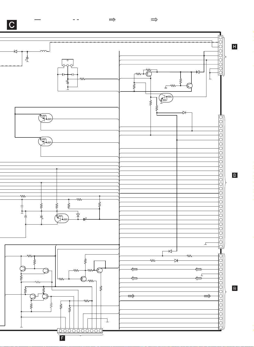
SCHEMATIC DIAGRAM - 9
: +B SIGNAL LINE
PANEL CIRCUIT
D613
B0BA5R600016
KRA102MTA
MOTOR ON/OFF
SWITCH
R637
PPHOTO_1
Q613
R918
PPHOTO_2
Q608
1K
100P
C609
100P
C607
47
Q611
PHOTOCURRENT AMPLIFIER
L601
G0C100JA0030
C640
50V3.3
Q609
KRA102MTA
SUPPLY CONTROL
SWITCH
(REC_H: HIGH)
Q609
Q608
100K
R646
Q600
50V1
C608
Q600
KRC103MTA
POWER RESET SWITCH
R920
10K
R916
100K
Q612
R917
56K
10K
R911
100K
R919
47
R915
KTC3199GRTA
R914
Q610-Q613
B3RAB0000025
REMOTE SENSOR
C638
1000P
100K
R645
DVREF+
KTA12710YTA
PLUNGER ON/OFF
R698
1K
Q610
56K
12K
R924
MODE_PB
10
TO MECHANISM CIRCUIT
(CN971) ON SCHEMATIC DIAGRAM-11
Z600
VDD
O
22K
R639
Q614-Q615
SWITCH
22K
R923
GND2
HALF_PB
8
9
: -B SIGNAL LINE : MAIN SIGNAL LINE
G
321
C637
0.01
R655
C639
6.3V47
R693
22K
R638
470
47
D617
B0AACK000004
C610
50V2.2
1K
R691
R689
22K
R692
2.7
R658
100K
PHOTO_2
PHOTO_1
/RESTSW
CHG_PLGR
CHG_HALF
CHG_CW
CHG_CCW
Q614
VREF+
RMT
SW5V
REC_H
REC_01
MOTOR
MOT_01
CDRST
SW1
SW2
DC_DET
SYNC
VREF+
PL2
MOT10V
PL1
Q615
2.7
R688
R921
10K
DECK1
DECK2
PPHOTO_2
DECK_2
PPHOTO_1
7
6
5
PL_GND
4
DVREF+
3
PPL1
2
PPL2
1
CP600
SYS6V
PCONT
SYNC
DVREF+
VREF+
SW5V
PLLCE
SD
STATUS
/CDRST
ST/DO/SQCK
SUBQ
LED9V
PLLCLK
BLKCLK
ASP_DAT
ASP_CLK
PLLDA
VREF+
DC_DET
CHG_CCW
CHG_CW
CHG_HALF
CHG_PLGR
SW2
SW1
/RESTSW
CHG_AD1
CHG_AD2
MOT10V
/CD
MUTEH
MUTEA
HPL
HPR
REC_01
SPEA
MIC_GND
MIC
+9V
DMT
H_DECK1
BP1
MOT_01
PL_GND
KTA1276GRTA
VREF SUPPLY SWITCH
R654
470K
R653
4.7K
R652
1K
R648
5.6K
R649
: MIC SIGNAL LINE
Q603
Q604
R647
22K
B0AACK000004
150
Q604
KTA1276GRTA
DECK SUPPLY SWITCH
R650
R651
470K
10K
Q605
Q605
KRC102MTA
PCONT SWITCH
D616
B0AACK000004
D615
B0AACK000004
D614
1SS380TE-17
R659
100K
D612
Q603
SYS6V
PCONT
SYNC
D.GND
D.GND
SW5V
MLD/PLLCE
PLLCE1
D.GND
STATUS
/CDRST
ST/DO/SQCK
SUBQ
LED9V
PLLCLK
BLKCLK
ASP_DAT
ASP_CLK
MDATA/PLLDA
VREF+
DC_DET
CHG_CCW
CHG_CW
CHG_HALF
CHG_PLGR
SW2
SW1
/RESTSW
CHG_AD1
CHG_AD2
AGND
MOT10V
MUTEH
MUTEA
HPL
HP_GND
HPR
REC_H
SPEANA
MIC_GND
+9V
RDS_DET
DMT
DECK1_H
MOTOR
PL_GND
FL2
-VP
FL1
SD
/CD
MIC
BP1
1
2
3
TO
4
TRANSFORMER
CIRCUIT
5
(CN951) ON
6
SCHEMATIC
DIAGRAM-13/14
7
8
9
H600/
W600
1
2
3
4
5
6
7
8
9
10
11
12
13
14
TO
15
MAIN CIRCUIT
(CN302) ON
16
SCHEMATIC
DIAGRAM-5
17
18
19
20
21
22
23
24
25
26
27
28
29
30
CP602
1
2
3
4
5
6
7
8
TO
9
MAIN CIRCUIT
(CN303) ON
10
SCHEMATIC
11
DIAGRAM-4
12
13
14
15
16
17
CP601
Page 90
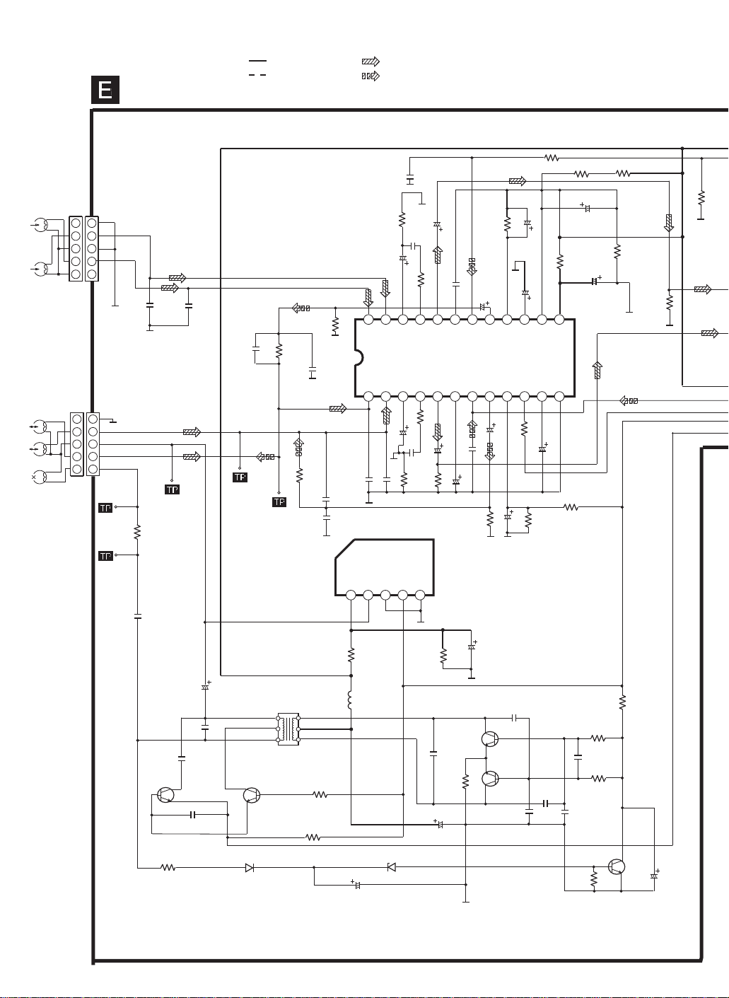
PLAYBACK
HEAD
RECORD/PLAY
HEAD
ERASE
HEAD
SCHEMATIC DIAGRAM -10
DECK CIRCUIT
1
1
L
R
L
R
2
3
4
5
CS1001
1
2
3
4
5
CS1002
2
3
4
5
1
2
3
4
5
L
R C1030
C1015
1000P
5
10
R1001
1
12
C1002
2.2
C1012
1000P
C1020
470P
4
: +B SIGNAL LINE
: -B SIGNAL LINE
IC1001
AN7348S-E1
P.B EQ/REC AMP/
ALC/TPS AMP
R1017
8.2K
R1009
18K
C1019
1000P
R1010
18K
3
INPUT
TAPE A
IC1001
TAPE B
1 2 3 4
1000P
C1023
C1021
470P
C1022
1000P
IC1004
VCC
SW
1 2 3 4 5
R1026
1K
: PLAYBACK SIGNAL LINE
: RECORD SIGNAL LINE
C1038
220P
R1015
C1034
47
50V3.3
C1032
0.018
10V100
3.9K
R1018
0.033
C1036
21222324
NF
EQ
INPUT
INPUT
C1027
TAPE A
TAPE B
1000P
INPUT
C1031
PB AMP
PB AMP
PB AMP
OUTPUT
ALC LOW
AB SW T
PB AMP
EQ
PB AMP
OUTPUT
5206197188179161015111412
3.9K
R1019
C1035
50V3.3
10K
R1022
C1037
50V3.3
10V100
47
R1016
PB AMP
NF
C1033
0.018
C1AA00000612
GND
CTRL2
CTRL1
R1005
4.7K
C1040
16V10
CUT
REC IN
REC IN
220P
C1039
R1028
IC1004
R/P SELECT
C1009
10V47
R1029
REC OUT
REC OUT
8.2K
4.7M
C1056
ALC T
REC/PB SW
16V10
C1041
R1030
C1043
50V4.7
16V10
100
C1042
HI/LO
AB SW
16V22
10V22
C1045
R1031
R1055
2.2K
220
R1090
13
CRO/NOR
RIPPLE
FILTER
OUTPUT
27K
VCC
GND
R1035
10k
R1038
4.7 K
C1044
10V33
C1046
10V220
R1039
15K
R1040
R1098
10K
0
R1032
10K
C1007
4700P
C1003
1500P
Q1001
C1001
0.01
R1003
10K
Q1001
KTC3875GRTA
SWITCHING
(BEAT PROOF)
C1006
50V1
Q1003
D1003
B0ACCK000005
Q1003
B1AAGC000006
SWITCHING
(RECH)
L1002
7L1A62N
6
5
4
3
2
1
R1004
R1006
1K
1.5K
L1001
RLQB470JTD-D
B0BC3R700004
C1008
50V1
D1004
Q1004-Q1005
B1AAGC000006
BIAS OSCILLATOR
C1011
0.047
R1007
4.7
C1010
25V100
C1014
1000P
Q1004
Q1005
C1016
2200P
C1013
1000P
C1017
2200P
KTC3875GRTA
BIAS OSC CONTROL
R1011
10K
R1012
4.7K
C1018
0.01
R1013
4.7K
Q1007
Q1007
R1014
4.7K
C1026
6.3V47
Page 91
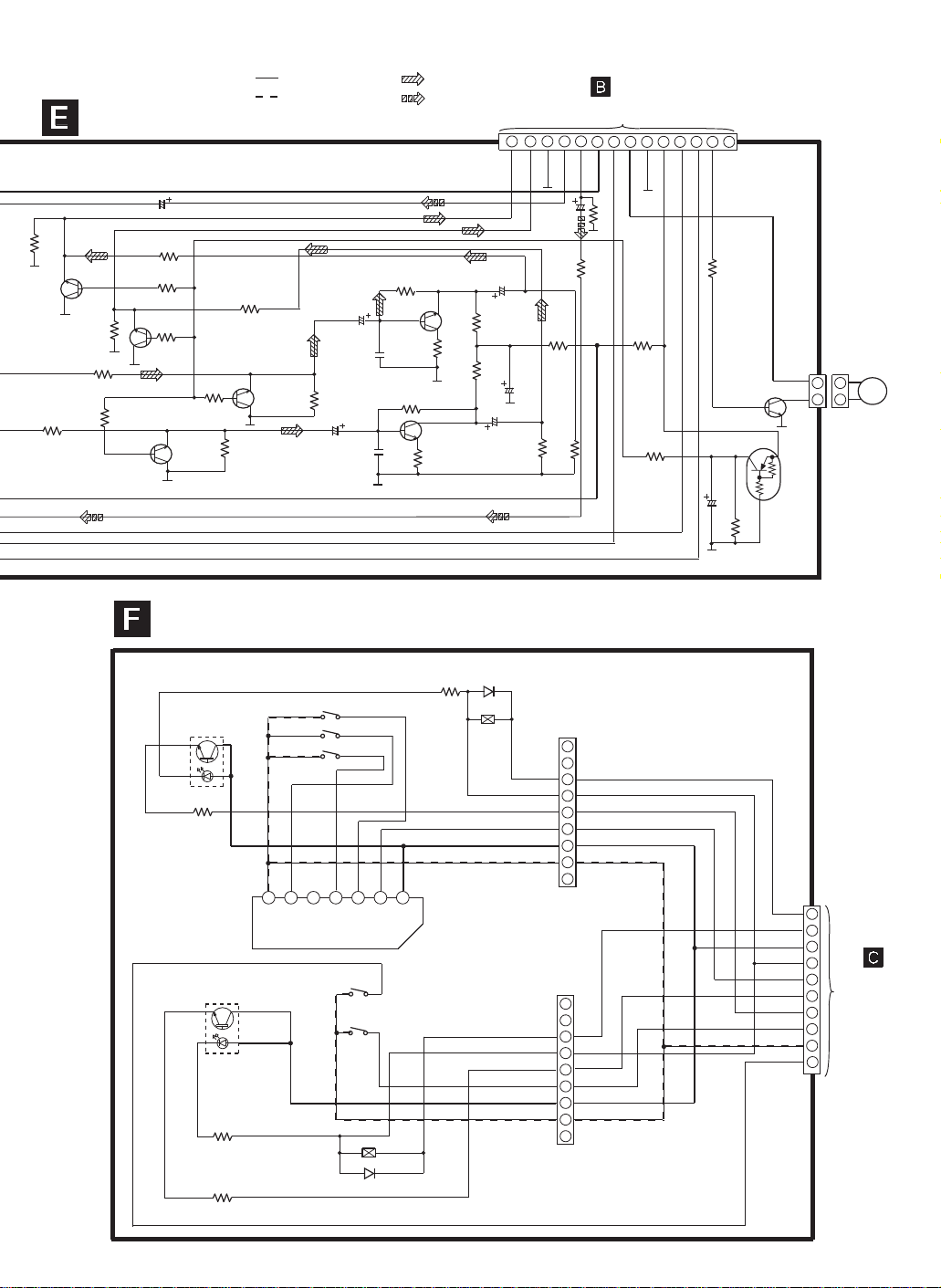
SCHEMATIC DIAGRAM - 11
DECK CIRCUIT
50V3.3
C1054
R1048
1K
R1091
2.2K
R1094
1K
R1093
1K
Q1021
Q1013
R1047
1K
R1095
100K
Q1020
Q1020-Q1021
KTD1304TA
MUTING SWITCH
R1086
2.2K
R1096
100K
R1084
2.2K
Q1012-Q1013
KTD1304TA
MUTING
R1046
100K
R1092
2.2K
Q1012
: +B SIGNAL LINE
: -B SIGNAL LINE
C1048
50V1
R1045
100K
C1047
50V1
Q1014-Q1015
2SC2412KT96R
BUFFER AMP
: PLAYBACK SIGNAL LINE
: RECORD SIGNAL LINE
R1049
1M
Q1014
C1049
1000P
R1050
1M
R1051
220
Q1015
C1050
R1052
1000P
220
R1053
680
R1054
680
C1052
50V1
C1051
50V1
14
PBOUTL
C1053
16V220
R1087
47K
TO
MAIN CIRCUIT (CN304) ON
SCHEMATIC DIAGRAM-4
10
1112
13
+B
AFGND
RECINL
RECINR
PBOUTR
C1064
50V3.3
R1057
2.2K
R1056
220
R1085
47K
REC_H
10K
R1097
MO+B
R1058
689 7
2.7K
R1061
5
DMT
MO GND
0
4
3
BP1
DECK1_H
2
MOTOR
CN1001
1
Q1017
KTD1146YTA
MOTOR SWITCH
R1060
390
Q1017
Q1016
C1055
50V0.1
10K
R1059
Q1016
KRA102STA
DECK MUTING SWITCH
121
W1002
M
2
MECHANISM CIRCUIT
IC971
CNB13030R2AU
PHOTO INTERRUPTER
S975
S972
S971
R973
39K
_R
HALF
VREF
_GND
Z971
RGSD12A1445T
IC951
CNB13030R2AU
PHOTO INTERRUPTER
R952
820
R953
39K
RECINH
RECINH_F
HALF
MODE
_F
MODE
RECINH
S951
MODE
S952
HALF
PL971
D951
MA2C16500E
1234567
AD_OUT
STBY
_5V
R972
820
D971
MA2C16500E
PL970
MODE
D1_CRO2
GND
PHOTO_T
HALF
STBY_5V
VREF_GND
PHOTO_S
MODE
D1_CRO2
GND
PHOTO_T
HALF
STBY_5V
VREF_GND
PL
PL2
1
PL1
2
STBY_5V
3
PL_GND
4
5
6
7
8
9
10
CN971
TO
PANEL
CIRCUIT
(CP600) ON
SCHEMATIC
DIAGRAM-9
AD_OUT
PHOTO_PB
PHOTO_RP
HALF_PB
PL
VREF_GND
MODE_PB
Page 92
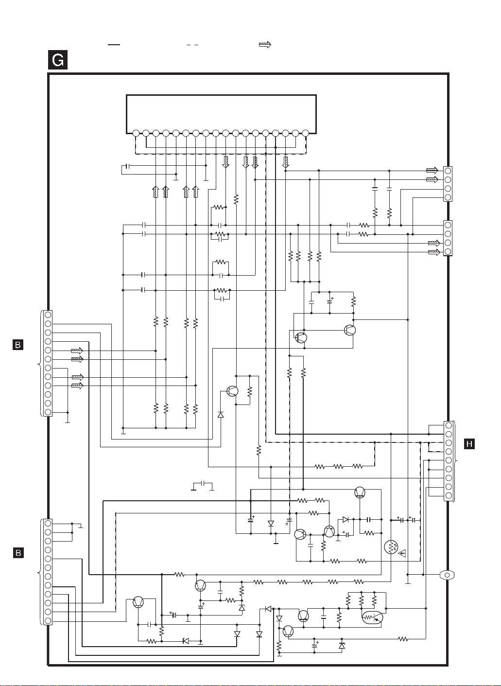
SCHEMATIC DIAGRAM - 12
TO
MAIN
CIRCUIT
(CN300) ON
SCHEMATIC
DIAGRAM-6
TO
MAIN
CIRCUIT
(CN301) ON
SCHEMATIC
DIAGRAM-6
CN500
CN501
POWER CIRCUIT
RSN315H42-P
POWER HIC
FAN
1
DC_DET
2
MUTE_H
3
+15V
4
HI_L
5
HI_R
6
A_GND
7
LO_L
8
LO_R
9
10
11
T GND
12
P GND
1
D GND
2
uP GND
3
4
CD8V
5
6
7
LED 9V
8
MOT10V
9
+9V
10
-9V
11
SW 5V
12
: +B SIGNAL LINE
IC501
C501
0.01
B1AAGC000006
MUTING SWITCH
B1AAKD000009
5V VOLTAGE REGUALTOR
KRA110MTA
CURRENT LIMITING SWITCH
(SHORT CIRCUIT PROTECTION)
Q508
D508
B0BA5R600016
-VD
+VD
C242
820P
C442
820P
C240
820P
C440
820P
Q514
HEADPHONE
Q508
Q506
C514
0.01
R532
150
-IN 2 1
-IN 2 2
IN GND
3.3K
3.3K
R445
R245
15K
15K
R446
R246
15V VOLTAGE REGULATOR
R524
2.2
C513
25V10
2.2K
R531
: -B SIGNAL LINE : MAIN SIGNAL LINE
IC501
-IN 1 1
-IN 1 2
OUT GND
-VCCM
OUT 1 2
AC DET
OUT 1 1
OUT 2 2
-VCC 1
+VCC 1
R250
10K
68K
R501
C243
15P
R450 68K
C443
15P
R249
68K
C241
15P
HOUT_GND
R449
68K
C441
3.3K
R247
15P
3.3K
R447
Q514
22K
D513
B0AACK000004
R522
3.3K
R523
470
D507
1T3T
R502
R503
12K
C508
16V10
D501
B0BA9R600002
D502
B0BA01500003
D504
B0AACK000004
R521
2.7
D503
MTZJ15CTA
D506
1T3T
D502
D505
1T3T
Q502
R520
15K
15K
R248
R448
C530
0.18
Q503
KTC2026
Q504
KTA1046
CURRENT STABILISER
SWITCH
Q507
KTC3199GRTA
10V VOLTAGE REGUALTOR
C509
0.01
Q503
C510
25V100
D508
C507
2.7
R529
OUT 2 1
16V10
D504
330
+VCC 2
23456789101112131415161718
56K
R451
R504
R511
560
Q504
Q507
47K
1
150K
R251
C506
R519
2.7
-VCC 2
Q512-Q513
B1AAGC000006
DC DETECT SWITCH
C244
0.047
C444
0.047
220K
100K
R452
R252
C503
C502
1000P
6.3V220
Q512
KTC2026
10V VOLTAGE REGULATOR
47K
R505
R512
2.7K
Q505
0.01
KTA1046
VOLTAGE SUPPLY SWITCH
KTA1267GRTA
CURRENT CONTROL SWITCH
R509
R508
330
330
R510
2.7K
D501
C505
16V100
3.3K
R513
R516
15
R518
2.7
R528
C511
10K
0.01
C512
25V33
C245
R255
10
R455
10
R506
100K
Q513
Q501
Q502
Q505
R507
330
Q501
C504
0.01
R514
3.3K
R515
27
R517
2.7
2.2
R525
R526
D509
B0BA9R600002
0.047
2.2
C445
R256
2.2
R527
Q506
0.047
10
R456
R530
10
C520
1.2K
50V2200
R533
SPKR_L_GND
SPKR_R_GND
SPKR_L_GND
SPKR_R_GND
C540
50V2200
C_GND
400
VCC+
VCC-
AC GND
ACIN
SUB B
SUB+B
GND
1
+
2
+
HIGH
CHANNEL
3
-
SPEAKER
-
4
JK951
-
1
-
2
LOW
+
CHANNEL
3
SPEAKER
+
4
JK952
1
2
3
TO
4
TRANSFORMER
CIRCUIT
5
(CN950)ON
6
SCHEMATIC
DIAGRAM-13/14
7
8
9
H950/
W950
E500
Page 93
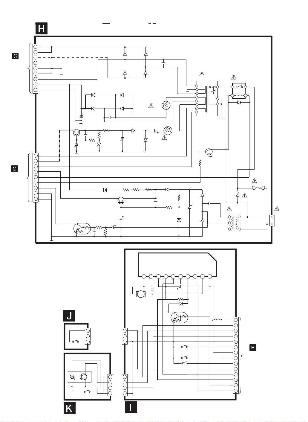
TO
POWER
CIRCUIT
(H950/
W950) ON
SCHEMATIC
DIAGRAM-12
TO
PANEL
CIRCUIT
(H600/
W600) ON
SCHEMATIC
DIAGRAM-9
SCHEMATIC DIAGRAM - 13
TRANSFORMER CIRCUIT (FOR GN ONLY)
VCC+
1
2
VCC-
3
4
AC GND
5
6
AC_IN
7
SUB B
8
SUB+B GND
9
CN950
1
2
3
4
5
6
7
8
9
CN951
Q951
2SB0621AHA
VOLTAGE REGULATOR
(-VP)
FL2
-VP
FL1
SYS6V
SYS6V
PCONT
SYNC
D_GND
ST_GND
KRC102MTA
SYCHRONISING
Q952
Q951
Q952
SWITCH
D954
C950
25V2200
C958
0.01
R961
C957
150
100V10
KTC3205YTA
VOLTAGE REGULATOR
D956
Q950
SYSTEM 6V
R958
10K
C954
0.01
: +B SIGNAL LINE : -B SIGNAL LINE
D950-D953
1N5402BM21
D954-D957
1T3T
C959
0.01
R959
4.7
R960
4.7K
D960
MTZJ27ATA
D966
1D3E
D955
D957
C956
63V100
R956
10
D952
D953
D959
1T3T
R955
10
R954
D950
D951
D958
1T3T
10
FP950
4000
C955
50V100
Q950
C953
0.01
C952
C963
35V4.7
R957
10K
10V47
B0BA6R600008
C960
D963
1D3E
0.1
FP951
1000
R953
150
D964
R952
T950
ETP76VMT61WA
Q953
B1AAGC000006
POWER CONTROL
SWITCH
RL950
RSY0040M-0
3
D965
1T3T
21
4
Q953
R951
3.3K
F1
125V 3.15A
FC2
T951
FC1
Z950
ERZV10V511CS
JK950
230V-240V
50Hz
D961
1D3E
D962
1D3E
C951
0.01
G4C2AAJ00001
1K
C961
16V1000P
CD DETECT
CIRCUIT
W2
3
2
1
SW4
D1
B0CAAD000002
D1
SW5
SPINDLE
POSITION
CIRCUIT
IC1
C0GAM0000005
MOTOR DRIVE
S
VCC
V
NC
9
10
8
7
C2
0.01
M
RM1
Q1
W2
3
2
1
4
4
3
3
2
2
1
1
W1
B1GACFGG0004
POWER SUPPLY
CONTROL
6
5
C1
16V100
R1 1K
D2
B0BA4R60003
SW2
SW1
SW3
Q1
4
VREF
NC
2
3
1
L
1
PLUNGER
POSITION
PSLED
D_GND
SW2
P_GND
SW1
OPEN
CLAMP
CCW
HALF
CW
2
3
4
5
6
TO
7
MAIN CIRCUIT
(CN309) ON
8
SCHEMATIC
9
DIAGRAM-4
10
11
12
13
14
CN1
BOTTOMSW
DRIVEPOWER
CD LOADING
CIRCUIT
Page 94
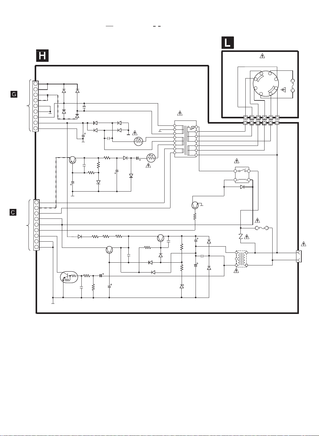
TO
POWER
CIRCUIT
(H950/
W950) ON
SCHEMATIC
DIAGRAM-12
TO
PANEL
CIRCUIT
(H600/
W600) ON
SCHEMATIC
DIAGRAM-9
SCHEMATIC DIAGRAM - 14
TRANSFORMER CIRCUIT (FOR GC ONLY)
D950-D953
1N5402BM21
D952
D953
Q951
Q952
Q952
D950
C960
0.1
D951
D954
D956
C950
25V2200
R960
C958
4.7K
0.01
R961
150
C957
100V10
Q950
KTC3205YTA
SYSTEM 6V
VOLTAGE REGULATOR
D966
R956
1D3E
10
Q950
R958
10K
R957
C954
0.01
CN950
CN951
VCC+
1
2
VCC-
3
4
AC GND
5
6
AC_IN
7
SUB B
8
SUB+B GND
9
FL2
1
-VP
2
FL1
3
SYS6V
4
SYS6V
5
PCONT
6
SYNC
7
D_GND
8
ST_GND
9
C963
35V4.7
10K
: +B SIGNAL LINE : -B SIGNAL LINE
D954-D957
1T3T
D955
C959
0.01
R959
4.7
C956
63V100
D960
MTZJ27ATA
D957
KRC102MTA
SYCHRONISING
D959
C955
1T3T
50V100
D958
1T3T
2SB621ARSTA
VOLTAGE REGULATOR
Q952
SWITCH
FP950
4000
FP951
1000
Q951
(-VP)
Q954
B1AAGC000007
CURRENT LIMITING
SWITCH
Q954
R955
R954
10
10
C952
10V47
C953
0.01
R963
820K
D968
B0AACK000004
D963
B0EAKM000085
C964
1000P
R952
D967
R953
D964
B0BA6R600008
T950
G4C7AFC00001
B1AAGC000006
C961
1K
150
Q953
POWER CONTROL
SWITCH
Q953
R951
3.3K
D961
16V1000P
C951
0.01
C962
16V1000P
D961,D962
1D3E
D967
B0EAKM000085
D962
VOLTAGE SELECTOR
CIRCUIT
S950
K0AFZA000005
VOLTAGE SELECTOR
5
6
240
W2A
W2A
RL950
RSY0040M-0
3
D965
1T3T
ERZV10V511CS
T951
G4C2AAJ00005
21
4
W6A
W6A
FC1
Z950
4
110
3
250V 2.5A
220
W7A
W7A
7
127
220
110
1
W3A
W3A
8
F2
250V 1.25A
W4A
W4A
127
240
2
W5A
W5A
F1
FC2
FC3
FC4
JK950
110V
127V
220V-230V
240V
50Hz/60Hz
Page 95

14 Printed Circuit Board
TOP PREVIOUS NEXT
Note: Circuit board diagrams may be modified at any time with the development of new technology.
TOP
PREVIOUS
NEXT
Page 96
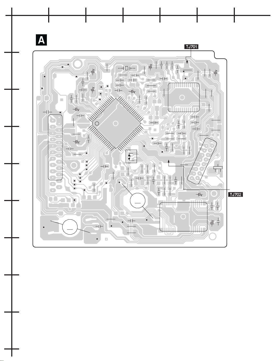
ABCDEFG
1
CD SERVO P.C.B (REPX0192D)
(RF)
TP20
C726
R718
80
1
TP11
TP7
TP6
TP3
J731
R717
C733
TP17
TP9
C728
TP25
TP26
C727
TP27
R753
TP24
C745
TP1
C753
CN702
19
17
15
13
11
9
7
5
3
1
TP23
TP22
18
16
14
12
10
8
6
4
2
TP21
C725
C730
C754
C743
TP5
TP4
TP2
C731
R721
J716
C732
J715
TP10
TP8
TP12
2
TP19
TP18
3
4
5
X701
J734
R714
C721
C744
C722
C724
60
61
IC702
20
21
J732
TP36
M702
SPL MOTOR
C717
C723
R731
R723
J721
TP28
S701
REST.SW
C738
M
R711
R741
41
40
R735
C703
R709
R712
R742
C718
TP42
C742
R724
R725
J724
TP33
R715
C715
C752
C704
C716
J701
R749
R727
28
C707
14
15
R705
R704
R728
R729
C706
C710
C749
C739
TJ701
TP30
C702
IC701
R702
C747
R744
R706
R707
J728
R736
TP29
TP29
R708
C714
28
14
1
12
1516
J709
C711
C712
C713
R750
11
13
15
J722
J710
4
56
78
910
R701
J727
J750
J702
J712
12
3
Q701
C750
C701
CN701
C
E
B
C751
(VREF)
6
TP37
M
M701
TRV MOTOR
C736
TP38
J704
TP16
TP15
C737
J707
J708
TP35
IC703
1
14
C735
C734
7
8
9
Page 97
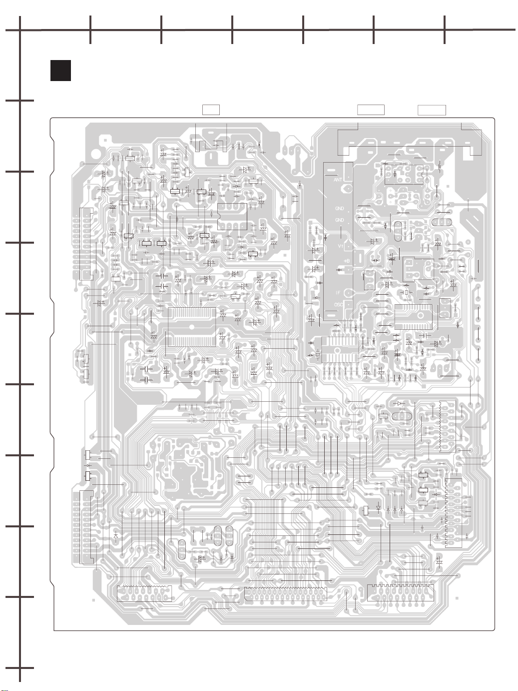
ABCDEFG
1
MAIN P.C.B. (REPX0325C...GC)
B
(REPX0325D...GN)
AUX
2
C430
R437
J366
C235
R243
3
4
5
CN300
12
11
10
9
8
7
6
5
4
J306
3
2
1
J377
J378
C319
J381
R256
Q207
B
C
R456
E
R255
Q407
B
C
E
R455
C435
R443
J228
R319
Q211
J382
Q404
R238
C231
J340
J339
ECB
R444
C434
Q405
R242
C234
R244
J288
J287
R274
R407
R406
C252
C251
R273
ECB
R272
R353
R271
J390
J286
ECB
R439
R438
C431
Q204
ECB
J305
R239
R237
R441
C433
Q205
J383
R222
C232
Q403
C403
J352
J304
R307
C318
R436
J350
R473
R454
C452
C230
C429
ECB
Q301
R236
J328
R440
C432
R442
J307
C233
R241
R240
J364
Q203
E
E
B
R408
C
C
R208
C203
R403
R405
R404
C419
C420
R422
R421
C308
R308
J333
J303
C305
C307
R221
C220
C218
C219
6
J278
D304
J244
J214
D302
D305
7
8
CN301
12
11
J235
10
9
8
7
6
5
4
3
2
1
J302
J234
J316
J257
J261
D309
CN304
J252
J385
J320
J321
J322
J323
J296
J314
14
12 1097865342
13 11
J207
J319
J318
J317
JK300
C332
C331
C201
R352
R471
J351
R472
C451
Q411
B
C
R474
R318
ECB
R309
B
R409
R209
R205
J347
C418
J389
21
C440
E
Q402
R310
R434
ECB
C309
R435
J329
J348
C312
C313
C240
R254
J222
J365
Q202
C
E
B
C229
R235
R234
R206
R204
R207
C221
R203
C417
C414
R420
R419
C415
C416
R356
C330
C306
1
IC300
22
J283
C217
R220
C405
J209
J224
Q310
J380
1
42
C213
C216
C215
C212
C214
R219
R218
R304
J388
R214
J233
B
C
E
R216
J248
R217
R417
C205
R415
R215
J245
R414
Q308
R311
R312
R313
C316
R315
R314
C315
J256
R316
J255
J379
C401
R433
R423
R432
R429
R460
D401
R426
C427
C426
C425
R427
R428
14
32
IC301
76
C226
C225
C227
R226
R260
R228
R227
R232
R233
C413
R458
R357
Q302
C311
C310
R305
C304
C208
R258
C211
R418
R416
J246
J272
J269
Q309
B
B
C
C
E
E
R317
D307
D308
J254
J230
J253
D201
R229
R223
C411
ECB
R201
C421
Q401
58
J211
J210
C202
R202
R401
C
R430
B
E
R424
C422
R425
C423
C223
R225
C222
R224
Q201
ECB
C412
R355
C407
J212
C406
C207
C209
J276
30
CN302
L301
C303
R431
C402
R402
R303
C424
J251
C224
C428
C228
R230
R231
C409
J250
C408
J387
J285
J284
J282
C206
J281
J249
J247
J327
J225
J226
J273
J274
J275
J242
J237
J238
J239
J299
J356
J355
J375
J374
J373
J262
J259
J372
J371
J370
J363
J295
2022
24 141210 8 6
23 211817
J100
D301
R111
R114
C110
R113
C125
J119
C111
R115
C112
D101
R128
J101
J107
C130
C132
R116
C133
20
C134
1
X103
R136
R137
R413
R412
C404
R410
R411
R213
C204
R211
R210
J215
J270
J326
J325
J241
J240
J268
J346
J345
J297
J258
J353
234
1
591113151619
72526272829
C101
IC102
R135
J298
J324
JK101
R134
R212
J267
J266
J264
FM ANT
12
R105
C122
D303
R103
J135
CF201
J105
J104
J336
R324
C102
3
2
1
R152
R130
CN303
R104
C104
J117
J145
C113
Q323
J357
J131
C107
5
4
R110
6
Z101
J134
C103
Q101
C147
C148
J115
C123
J112
J110
J109
J108
J106
C117
C118
C141
C137
C121
R122
R141
C301
Q324
ECB
R341
R342
R343
J271
R322
R320
R321
D306
D321
D320
J391
J315
15
Z120
1
2
J126
3
J123
4
J122
5
6
7
8
R127
R129
R151
R132
C124
11
10
R117
R133
R138
J133
J221
J220
J217
J216
R301
J338
J337
J301
J263
J206
J205
75 OHMS
R112
7
8
9
C108
J124
B
R106
C
E
R107
Z102
C129
4
J118
5
3
C149
X102
R124
12
IC101
13
C139
C142
R123
C138
C143
R142
R145
D324
R350
EB
C
R349
R347
R346
R340
J354
J300
R335
R334
R302
R336
R323
R325
D322
J232
J231
J386
J313
C131
R146
Q321
J265
AM ANT
4
3
J130
1
L102
3
J129
2
J128
J127
J223
J125
Q106
EB
C
R101
6
C126
R102
R143
C144
J213
Q322
ECB
ECB
Q320
C116
C120
J277
C317
J121
C127
J120
R125
R126
C109
J132
2
J116
1
C106
J111
24
C119
R121
R348
R345
R344
J243
ECB
J227
117
23457689101112131416
R131
R144
R118
J113
J114
CF202
1
1
2
3
J144
C115
J150
CN309
2
J219
4
6
8
10
12
14
R326
C325
R337
R327
CN310
C324
R338
D323
R339
C323
C322
C320
J208
C329
J200
C302
C114
J201
R119
J202
C136
J203
R120
J103
J204
J280
J279
1
3
J218
5
7
J360
9
11
C326
13
J384
J362
J361
R333
R332
1
2
3
4
R328
5
6
7
R329
8
R330
9
10
R331
11
12
13
14
15
16
17
C321
18
19
9
Page 98
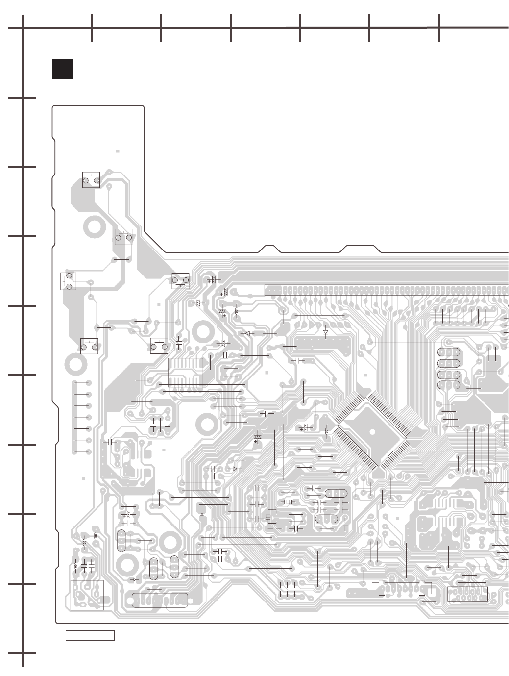
ABCDEFG
R
R
R
R
4
J
6
1
C
PANEL P.C.B. (REPX0326D...GC)
(REPX0326C...GN)
2
S606
OPEN/CLOSE
R606
3
S607
CD1
R607
4
5
6
7
8
9
S608
CD2
L604
7
J947
J946
J945
J944
J943
J942
J941
6
S609
CD3
L602
C621
2
1
JK601
R608
L603
3
4
R609
J651
C620
5
C648
C602
C601
E
C
B
Q603
R675
J611
J910
D612
R611
R610
J645
J668
R650
1
J911
R652
R651
Q604
R654
J665
S610
CD4
R614
C634
R613
R681
R628
E
C
B
J630
H600/W600
C657
9
10
Q605
E
C
R653
B
S611
CD5
IC603
C635
98765432
J603
J614
C661
J689
J935
J936
J912
J928
18
C650
1
D611
J605
C659
C649
J914
R680
J920
C641
C640
C660
C656
J615
J691
C646
C647
R657
R656
J639
J915
R630
J690
L601
J637
J931
D613
D610
J694
J666
J667
C607
C600
R631
C651
C645
J927
J609
C604
J904
X602
C618
J629
J608
J669
J902
R640
X601
C652
R627
C653
C603
J925
R643
R644
C617
C654
J698
C605
R699
R632
R642
Q601
C655
C612
C611
105115253035404520
J901
D605
R626
J602
C606
100
1
L600
R635
J687
C614
Q602
C
EB
C613
C616
B
C
E
R641
J677
J657
J636
J660
J652
C615
J641
81
80
IC600
30
J695
R615
J678
R629
J676
R634
J622
CN900
31
R616
1
J696
J635
FL600
J929
J632
J675
51
50
Q610
Q611
Q612
Q613
8
765432
J618
J674
R923
R672
R671
R911
R919
R670
CEB
CEB
CEB
CEB
R916
R920
J628
CP600
R669
R633
1
2345678
R668
J670
J613
J656
R667
R917
R918
J671
R924
R666
J606
J903
9
10
R665
R915
J643
J693
R914
J654
R647
R648
J624
R921
R692
R688
J6
R
J625
J
HEADPHONE
Page 99
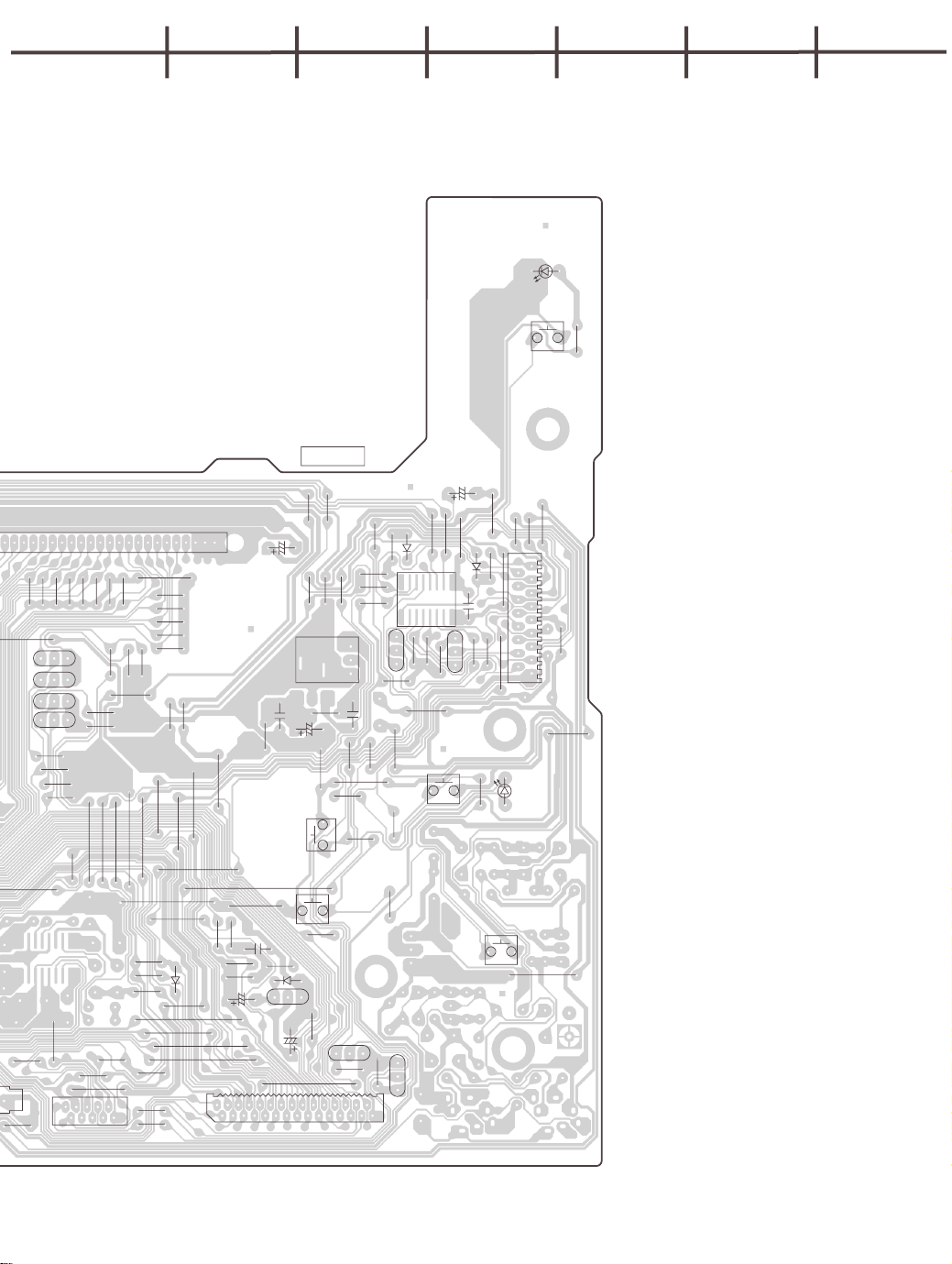
GHI J K L M
35 40 45 50 53
R671
R667
R669
R670
R668
CEB
CEB
CEB
CEB
J628
1
CP600
R917
R918
J670
R633
J613
J656
2345678
J671
R924
R666
J606
J903
9
10
R665
R915
J643
J693
8
610
611
612
613
J618
J674
R923
R672
R911
R919
R916
R920
R914
J654
R647
R648
J624
R921
R692
R688
J644
J625
R664
R663
R662
R661
R660
J673
J648
J938
J601
J937
J692
J626
J672
J631
J633
C609
R637
R636
R658
R639
C610
D616
J638
J679
J917
J627
J916
1
2345678910111213141516171819202122232425262728
CP602
R655
R638
C642
C637
CEB
C608
SENSOR
J640
R612
Z600
J697
C639
J683
S605
REC
DECK1/2
R645
D617
Q600
R646
J921
J642
J604
J699
1
3
R605
R687
S604
Q615
CEB
R693
2
C638
J619
R604
R619
R618
R617
J684
29
30
J610
Q614
R689
R649
E
C
Q608
B
J621
J649
R601
R603
E
C
B
D614
8
9
J686
IC601
R623
R622
J650
J623
Q609
S602
SSEQ
J688
1
16
C658
J682
E
C
B
D615
R698
R602
J616
R659
C636
R691
S603
RESET
J685
J612
J620
2
4
6
8
10
12
14
16
CP601
D609
D600
POWER
J607
1
3
5
7
9
11
13
15
17
J634
S601
R600
J617
J681
J647
Page 100
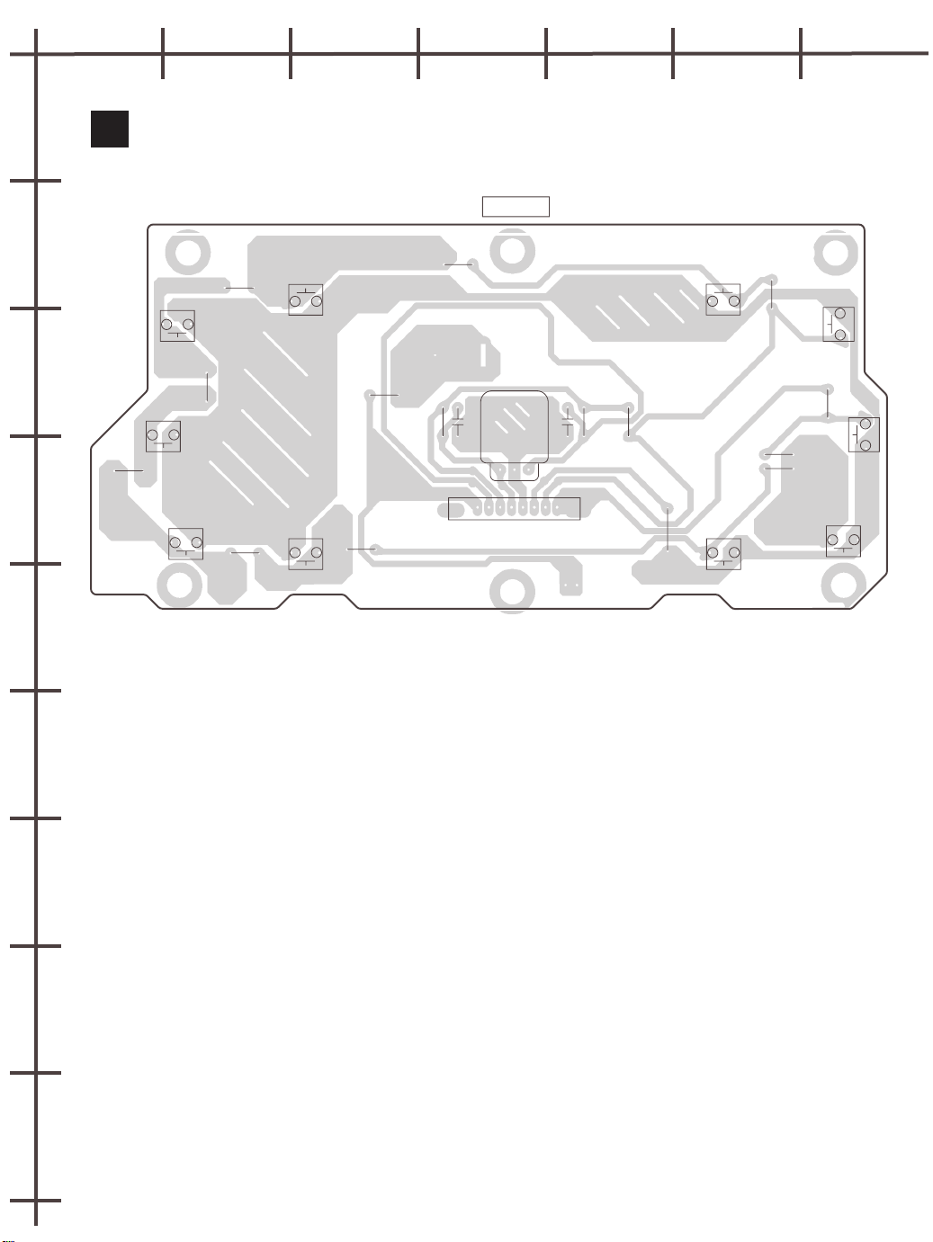
ABCDEFG
1
TACT SWITCH P.C.B. (REPX0326D...GC)
D
(REPX0326C...GN)
VOLUME
2
R903
S904
FF
S903
CD PLAY
3
J932
R905
R904
S905
STOP
4
S906
R906
DECK2 OPEN
S907
TAPE
R907
R902
R913
CP900
C902
1 3456782
VR600
1
2
S902
R901
TUNER
R912
C901
3
R900
J933
R909
R908
S908
AUX
S901
REW
S910
R910
DISPLAY
S909
DECK1 OPEN
5
6
7
8
9
 Loading...