

Panasonic PNA4611M, PNA4612M, PNA4613M, PNA4614M, PNA4620M Datasheet
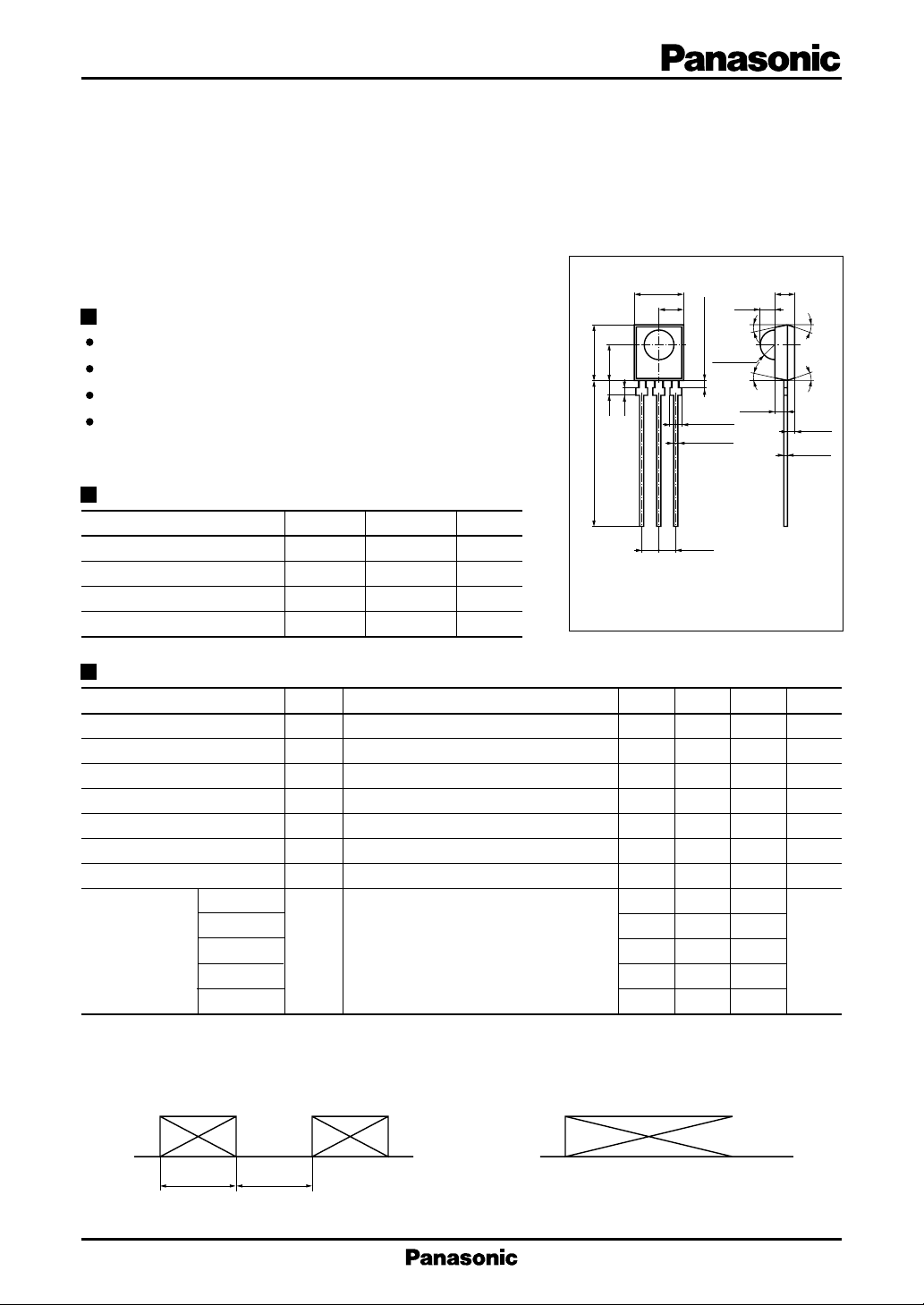
Photo IC
PNA4611M Series
(PNA4611M/4612M/4613M/4614M/4620M)
Bipolar Integrated Circuit with Photodetection Function
For infrared remote control systems
Features
High sensitivity (extension distance is 11 m or more)
External parts not required
Resin to cutoff visible light is used
Supports various metal holders with improved electromagnetic
noise resistance
Absolute Maximum Ratings (Ta = 25˚C)
Parameter Symbol Ratings Unit
Power supply voltage V
Power dissipation P
Operating ambient temperature
Storage temperature T
T
– 0.5 to +7 V
CC
D
–20 to +75 ˚C
opr
– 40 to +100 ˚C
stg
200 mW
Main Characteristics (Ta = 25˚C VCC = 5V)
Parameter Symbol Conditions min typ max Unit
Operating supply voltage V
Current consumption I
Maximum reception distance
Low-level output voltage V
High-level output voltage V
Low-level pulse width T
High-level pulse width T
PNA4611M 36.7
PNA4612M 38.0
Carrier frequency
PNA4613M f
PNA4614M 56.9
PNA4620M 33.3
Note 1) Fig.1 burst wave, L=L
Note 2) Fig.2 continuous wave, L ≤ L
Note 3) Light shut off condition
Carrier wave : f
, 16 pulses
max
L
max
CC
Note 3 1.8 2.4 3.0 mA
CC
Note 1 11 16 m
max
Note 2 0.35 0.5 V
OL
Note 3 4.8 5.0 V
OH
Note 1 200 400 600 µs
WL
Note 1 200 400 600 µs
WH
0
0
7.0±0.2
3.5
8.0±0.2
5.2
2.3
22.0 min.
0.8
123
R2.25±0.1
Not soldered 1.5
3-1.5±0.2
3-0.5
2-2.54
4.7 5.0 5.3 V
40.0 kHz
Carrier wave : f
0
+0.2
–0.15
2.25
2.0±0.1
5˚
5˚
CC
Unit : mm
5.25±0.3
5˚
5˚
1.0±0.1
0.45±0.2
1: V
OUT
2: GND
3: V
CC
V
400µs
400µs
Fig.2Fig.1
1
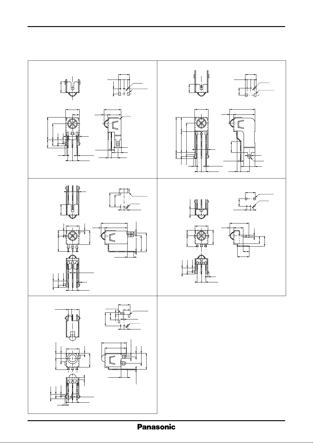
Photo IC PNA4611M, PNA4612M, PNA4613M, PNA4614M, PNA4620M
Type YA
12.712.74.9
Type XB
Type HB
2-2.54
Unit : mm
Type YB
7.6
4.0
3-ø0.9
2-2.4×1.4
5
2-2.54
5.5
Unit : mm
7.6
3-ø0.8
2-2.4×1.4
Recommendation hole location of P.C.board Recommendation hole location of P.C.board
18.3
1.2
1.0
3.1
(6.9)
(3.6)
7.6
123
123
7.6
7.4
3-0.5±0.2
2-2.54
8.5
7.6
3.8
9.6
2.0
1.2
(7.4)
3.5
123
1.0
3-0.5
2-2.54
+0.25
–0.15
123
7.3
6.5 6.5
7.6
2.5
3.1
0.8
8.5
(9.7)
10.35
2.25
(8.1)
R1.0
0.45
+0.25
–0.15
2.0
4.0
(4.0)(2.1)
1: V
O
2: GND
3: V
CC
Unit : mm
2-3.75
2-1.7×1.2
10.45
2-2.54
3-ø0.9
8.75
Recommendation hole location of P.C.board
16
(13.75)2.25
+0.25
2-1.4
–0.15
0.45
(9.6)
(11.3)
21.43.5
Type XD
12.9 8.5
2.0
3.7±0.6
2.4
1.6
+0.25
3-0.5
2.4
1.6
3.6
123
–0.15
0.6
2-2.54
8.8
4.42.0±0.1
0.8×2.2
5.55
10.08
4.85
1.45
2-2.2×1.2
0.45
3-ø0.9
1: V
O
2: GND
3: V
CC
Unit : mm
3.6
1.0
2-2.54
15.7
13.452.25
(6.8)
0.45±0.2
2.0
R1.0
7.0
1: V
(5.5)2.35
O
2: GND
3: V
CC
Unit : mm
7.8
2-1.8×1.2
5.9
2-2.54
Recommendation hole location of P.C.board
11.4
5.52.25
3-ø0.9
1.5
4.4
(5.9)
3.6
7.0
1: V
O
2: GND
3: V
CC
2-2.54
Recommendation hole location of P.C.board
3.2
(11.9)
7.7
(3.15)
5.4
1.2
8.7
(6.9)
1.3
1.6
0.93
2.9
0.9
3-0.5
2-2.54
+0.25
–0.15
9.97 2.9
3.7±0.6
6.4
2.1
2-2.0±0.1
(9.83)
+0.25
–0.15
0.45
1: V
O
2: GND
3: V
CC
Note :Tolerance unless otherwise specified is ±0.5.
2
 Loading...