

Page 1
查询KFG2816D1M-DEB供应商
OneNAND128 FLASH MEMORY
OneNAND SPECIFICATION
Product Part No. VCC(core & IO) Temperature PKG
KFG2816Q1M-DEB 1.8V(1.7V~1.95V) Extended 67FBGA(LF)/48TSOP1
OneNAND128
KFG2816D1M-DEB 2.65V(2.4V~2.9V) Extended
KFG2816U1M-DIB 3.3V(2.7V~3.6V) Industrial 67FBGA(LF)/48TSOP1
67FBGA(LF)/48TSOP1
Version: Ver. 1.0
Date: June 15th, 2005
1
Page 2

OneNAND128 FLASH MEMORY
INFORMATION IN THIS DOCUMENT IS PROVIDED IN RELATION TO SAMSUNG PRODUCTS,
AND IS SUBJECT TO CHANGE WITHOUT NOTICE.
NOTHING IN THIS DOCUMENT SHALL BE CONSTRUED AS GRANTING ANY LICENSE,
EXPRESS OR IMPLIED, BY ESTOPPEL OR OTHERWISE,
TO ANY INTELLECTUAL PROPERTY RIGHTS IN SAMSUNG PRODUCTS OR TECHNOLOGY. ALL
INFORMATION IN THIS DOCUMENT IS PROVIDED
ON AS "AS IS" BASIS WITHOUT GUARANTEE OR WARRANTY OF ANY KIND.
1. For updates or additional information about Samsung products, contact your nearest Samsung office.
2. Samsung products are not intended for use in life support, critical care, medical, safety equipment, or similar
applications where Product failure could result in loss of life or personal or physical harm, or any military or
defense application, or any governmental procurement to which special terms or provisions may apply.
OneNAND
rightful owners.
Copyright
™‚ is a trademark of Samsung Electronics Company, Ltd. Other names and brands may be claimed as the property of their
© 2005, Samsung Electronics Company, Ltd
2
Page 3

OneNAND128 FLASH MEMORY
Document Title
OneNAND
Revision History
Revision No.
0.0
0.1
1.0
History
1. Initial Issue.
1. Corrected the errata
2. Revised Cold Reset
3. Added TSOP1 Package Information
4. Revised FBGA package type
5. Added 67FBGA Package Information
6. Revised typical tOTP, tLOCK from 300us to 600us
7. Revised max tOTP, tLOCK from 600us to 1000us
8. Deleted Lock All Block, Lock-Tight All Block Operation
9. Added Endurance and Data Retention
10. Revised Load Data into Buffer Operation Sequence
11. Revised Warm Reset
12. Revised Programmable Burst Read Latency Timing Diagram
13. Revised Multi Block Erase Flow Chart
14. Revised Extended Operating Temperature
1. Added Copyright Notice in the beginning
2. Corrected Errata
3. Updated Icc2, Icc4, Icc5, Icc6 and I
4. Revised INT pin description
5. Added OTP erase case NOTE
6. Revised case definitions of Interrupt Status Register
7. Added a NOTE to Command register
8. Added ECClogSector Information table
9. Removed ’data unit based data handling’ from description of Device
Operation
10. Revised description on Warm/Hot/NAND Flash Core Reset
11. Revised Warm Reset Timing
12. Revised description for 4-, 8-, 16-, 32-Word Linear Burst Mode
13. Revised OTP operation description
14. Added note for OTP
15. Removed all block lock default case after cold or warm reset
16. Added explanation for each prohibited case in protect mode
17. Revised the case of writing other commands during Multi Block Erase
routine
18. Added note for Erase Suspend/Resume
19. Added supplemental explanation for ECC Operation
20. Removed classification of ECC error from ECC Operation
21. Removed redundant sentance from ECC Bypass Operation
22. Added technical note for Boot Sequence
23. Added technical note for INT pin connection guide
24. Excluded tOEH from Asynchronous Read Table
25. Revised Asycnchronous Read timing diagram for CE
26. Revised Asynchronous Write timing diagram for CE
27. Revised Load operation timing diagram for CE
in Internal Register Reset
L
SB
don’t care mode
don’t care mode
don’t care mode
Draft Date
Sep. 9, 2004
Oct. 28, 2004
Jun. 15, 2005
Remark
Advance
Advance
The attached datasheets are prepared and approved by SAMSUNG Electronics. SAMSUNG Electronics CO., LTD. reserve the right
to change the specifications. SAMSUNG Electronics will evaluate and reply to your requests and questions about device. If you have
any questions, please contact the SAMSUNG branch office near you.
3
Page 4

OneNAND128 FLASH MEMORY
1. FEATURES
♦ Architecture
• Design Technology: 0.12µm
• Voltage Supply
- 1.8V device(KFG2816Q1M) : 1.7V~1.95V
- 2.65V device(KFG2816D1M) : 2.4V~2.9V
- 3.3V device(KFG2816U1M) : 2.7V~3.6V
• Organization
- Host Interface:16bit
• Internal BufferRAM(3K Bytes)
- 1KB for BootRAM, 2KB for DataRAM
• NAND Array
- Page Size : (1K+32)bytes
- Block Size : (64K+2K)bytes
♦ Performance
• Host Interface type
- Synchronous Burst Read
: Clock Frequency: up to 54MHz
: Linear Burst - 4 , 8 , 16 , 32 words with wrap-around
: Continuous Sequential Burst(512 words)
- Asynchronous Random Read
: Access time of 76ns
- Asynchronous Random Write
• Programmable Read latency
• Multiple Sector Read
- Read multiple sectors by Sector Count Register(up to 2 sectors)
• Multiple Reset
- Cold Reset / Warm Reset / Hot Reset / NAND Flash Reset
• Power dissipation (typical values, C
- Standby current : 10uA@1.8V device, 15uA@2.65V/3.3V device
- Synchronous Burst Read current(54MHz) : 12mA@1.8V device, 20mA@2.65V/3.3V device
- Load current : 20mA@1.8V device, 20mA@2.65V/3.3V device
- Program current: 20mA@1.8V device, 20mA@2.65V/3.3V device
- Erase current: 15mA@1.8V device, 18mA@2.65V/3.3V device
• Reliable CMOS Floating-Gate Technology
- Endurance : 100K Program/Erase Cycles
- Data Retention : 10 Years
L=30pF)
♦ Hardware Features
• Voltage detector generating internal reset signal from Vcc
• Hardware reset input (RP
• Data Protection
- Write Protection mode for BootRAM
- Write Protection mode for NAND Flash Array
- Write protection during power-up
- Write protection during power-down
• User-controlled One Time Programmable(OTP) area
• Internal 2bit EDC / 1bit ECC
• Internal Bootloader supports Booting Solution in system
)
♦ Software Features
• Handshaking Feature
- INT pin: Indicates Ready / Busy of OneNAND
- Polling method: Provides a software method of detecting the Ready / Busy status of OneNAND
• Detailed chip information by ID register
♦ Packaging
• Package
- 67ball, 7mm x 9mm x max 1.0mmt , 0.8mm ball pitch FBGA
- 48 TSOP 1, 12mm x 20mm, 0.5mm pitch
4
Page 5

OneNAND128 FLASH MEMORY
2. GENERAL DESCRIPTION
OneNAND is a single-die chip with standard NOR Flash interface using NAND Flash Array. This device is comprised of logic and
NAND Flash Array and 3KB internal BufferRAM. 1KB BootRAM is used for reserving bootcode, and 2KB DataRAM is used for buffering data. The operating clock frequency is up to 54MHz. This device is X16 interface with Host, and has the speed of ~76ns random
access time. Actually, it is accessible with minimum 4clock latency(host-driven clock for synchronous read), but this device adopts the
appropriate wait cycles by programmable read latency. OneNAND provides the multiple sector read operation by assigning the number of sectors to be read in the sector counter register. The device includes one block sized OTP(One Time Programmable), which
can be used to increase system security or to provide identification capabilities.
5
Page 6
OneNAND128 FLASH MEMORY
3. PIN DESCRIPTION
Pin Name Ty pe Nameand Description
Host Interface
Address Inputs
A15~A0 I
DQ15~DQ0 I/O
INT O
RDY O
CLK I
WE
AVD I
RP
CE
OE
Power Supply
CC-Core/Vcc
V
V
CC-IO/Vccq
V
SS Ground for OneNAND
etc.
DNU
NC
- Inputs for addresses during operation, which are for addressing
BufferRAM & Register.
Data Inputs/Outputs
- Inputs data during program and commands during all operations, outputs data during memory array/
register read cycles.
Data pins float to high-impedance when the chip is deselected or outputs are disabled.
Interrupt
Notifying Host when a command has completed. It is open drain output with internal resistor(~50kohms).
After power-up, it is at hi-z condition. Once IOBE is set to 1, it does not float to hi-z condition even when
the chip is deselected or when outputs are disabled.
Ready
Indicates data valid in synchronous read modes and is activated while CE
Clock
CLK synchronizes the device to the system bus frequency in synchronous read mode.
The first rising edge of CLK in conjunction with AVD
Write Enable
I
WE
controls writes to the bufferRAM and registers. Datas are latched on the WE pulse’s rising edge
Address Valid Detect
Indicates valid address presence on address inputs. During asynchronous read operation, all addresses
are latched on AVD
CLK’s rising edge while AVD
> Low : for asynchronous mode, indicates valid address ;for burst mode,
causes starting address to be latched on rising edge on CLK
> High : device ignores address inputs
Reset Pin
I
When low, RP resets internal operation of OneNAND. RP status is don’t care during power-up
and bootloading.
Chip Enable
I
CE-low activates internal control logic, and CE-high deselects the device, places it in standby state,
and places ADD and DQ in Hi-Z
Output Enable
I
OE
-low enables the device’s output data buffers during a read cycle.
Power for OneNAND Core
This is the power supply for OneNAND Core.
Power for OneNAND I/O
This is the power supply for OneNAND I/O
Vcc-IO is internally connected to Vcc-Core, thus should be connected to the same power supply.
Do Not Use
Leave it disconnected. These pins are used for testing.
No Connection
Lead is not internally connected.
’s rising edge, and during synchronous read operation, all addresses are latched on
is held low for one clock cycle.
low latches address input.
is low
NOTE:
Do not leave power supply(V
CC, VSS) disconnected.
6
Page 7

OneNAND128 FLASH MEMORY
4. PIN CONFIGURATION
4.1 TSOP1
N.C
A15
A14
A13
A12
A11
A10
A9
A8
WE
V
SS
V
CC
INT
AVD
RP
A7
A6
A5
A4
A3
A2
A1
A0
N.C
1
2
3
4
5
6
7
8
9
10
11
12
13
14
15
16
17
18
19
20
21
22
23
24
48-pin TSOP1
Standard Type
12mm x 20mm
0.5mm pitch
(TOP VIEW, Facing Down)
TSOP1 OneNAND Chip
48pin, 12mm x 20mm, 0.5mm pitch TSOP1
48
47
46
45
44
43
42
41
40
39
38
37
36
35
34
33
32
31
30
29
28
27
26
25
V
SS
OE
DQ15
DQ7
DQ14
DQ6
V
CC
DQ13
DQ5
DQ12
DQ4
DQ11
DQ3
DQ10
DQ2
V
SS
DQ9
DQ1
DQ8
DQ0
RDY
CLK
CE
V
CC
Q
7
Page 8
OneNAND128 FLASH MEMORY
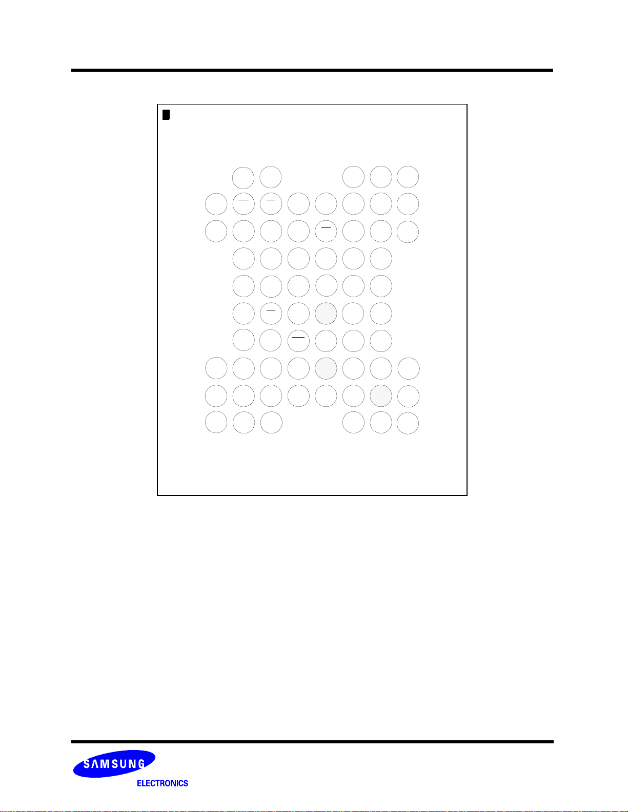
4.2 67FBGA
NC
NC
WE RP DQ14
NC
DQ12 DQ8 DQ1 OE DQ9
NC
DQ7 DQ4 DQ11 DQ10 DQ3
DQ15 A12 DQ0 DQ5 DQ6
CLK
CE DQ2 NC NC A9
A14
A13
NC
INT A0 A1 NC A10 A6
NC
NC
A4 A5 A2 A3 NC
RDY
NC NC
VSS VSS
A15
AVD A7 A11 A8
NC NC
DQ13
VCC
Core
VCC
NC NC
NC
NC
NC
IO
NC
NC
NC
(TOP VIEW, Balls Facing Down)
67ball FBGA OneNAND Chip
67ball, 7.0mm x 9.0mm x max 1.0mmt , 0.8mm ball pitch FBGA
8
Page 9

OneNAND128 FLASH MEMORY
TERMS, ABBREVIATIONS AND DEFINITIONS
B (capital letter) Byte, 8bits
W (capital letter) Word, 16bits
b (lower-case letter) Bit
ECC Error Correction Code
Calculated ECC ECC which has been calculated during load or program access
Written ECC ECC which has been stored as data in the NAND Flash Array or in the BufferRAM
BufferRAM On-chip Internal Buffer consisting of BootRAM and DataRAM
BootRAM A 1KB portion of the BufferRAM reserved for Bootcode buffering
DataRAM A 2KB portion of the BufferRAM reserved for Data buffering
Memory NAND Flash array which is embedded on OneNAND
Partial unit of page, of which size is 512B for main area and 16B for spare area data.
Sector
Data unit
It is the minimum Load/Program/Copy-Back program unit while one~two sector operation is
available
Possible data unit to be read from memory to BufferRAM or to be programmed to memory.
- 528B of which 512B is in main area and 16B in spare area
- 1056B of which 1024B is in main area and 32B in spare area
9
Page 10
OneNAND128 FLASH MEMORY
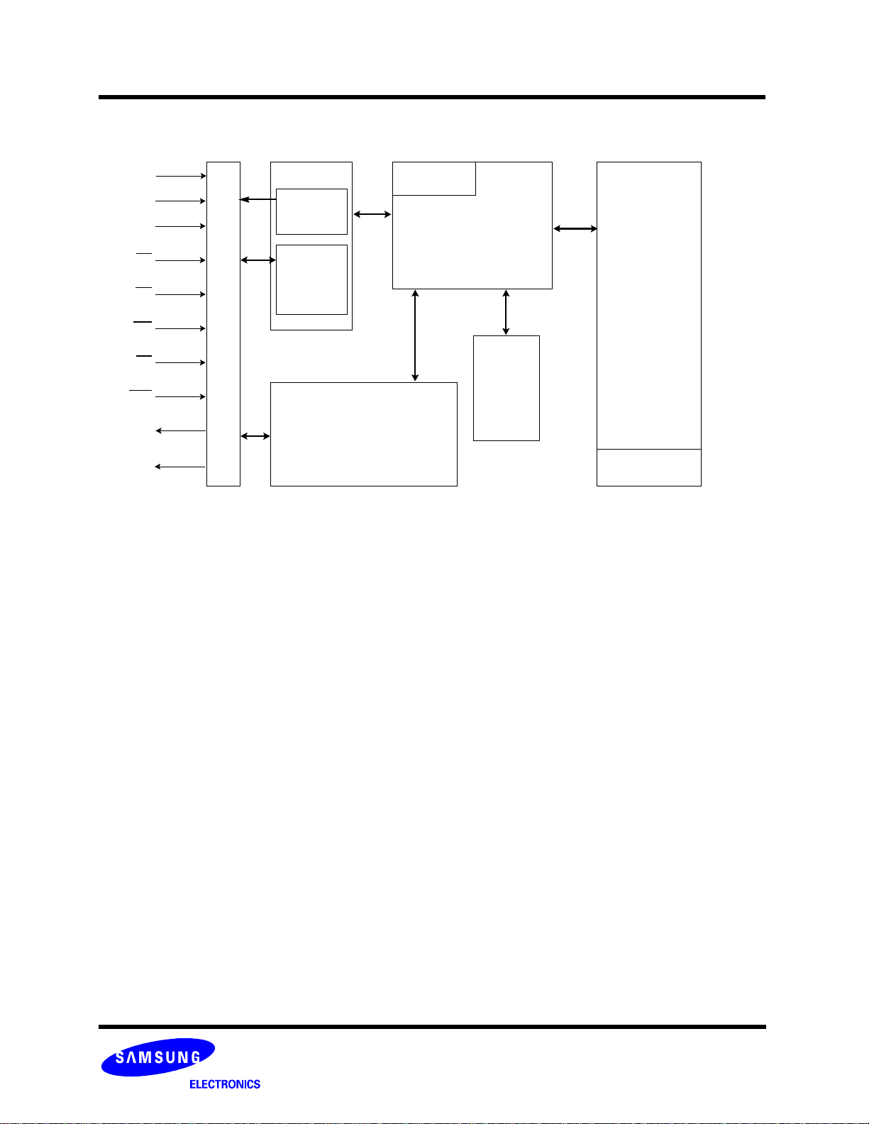
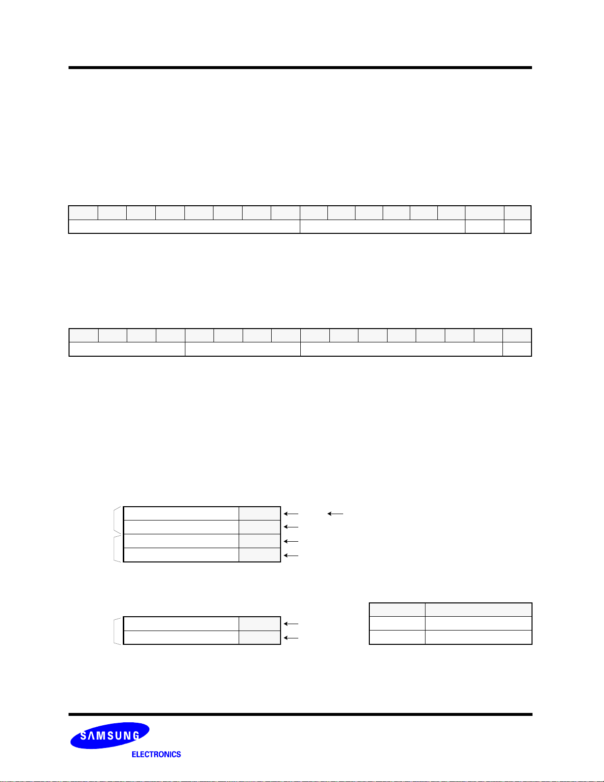
5. BLOCK DIAGRAM
DQ15~DQ0
A15~A0
CLK
CE
Host Interface
OE
WE
RP
AVD
INT
RDY
- Host Interface
- BufferRAM(BootRAM, DataRAM)
- Command and status registers
- State Machine (Bootloader is included)
- Error Correction Logic
- Memory(NAND Flash Array, OTP)
BufferRAM
BootRAM
DataRAM
Internal Registers
(Address/Command/Configuration
/Status Registers)
Bootloader
StateMachine
NAND Flash
Array
Error
Correction
Logic
OTP
(One Block)
NOTE:
1) At cold reset, bootloader copies boot code(1K byte size) from NAND Flash Array to BootRAM.
Figure 1. Internal Block Diagram
10
Page 11
OneNAND128 FLASH MEMORY
BootRAM
DataRAM 0
DataRAM 1
Main area data
(512B)
{
BootRAM 0
BootRAM 1
DataRAM 0_0
DataRAM 0_1
Main area data
(512B)
{
DataRAM 1_0
DataRAM 1_1
(BufferRAM)
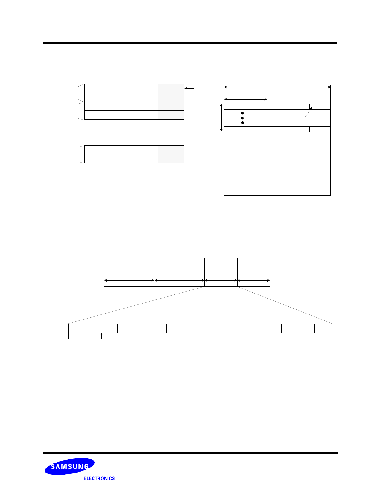
Figure 2. BufferRAM and NAND array structure
Spare area data
(16B)
{
Spare area data
(16B)
{
Sector
Block:
64pages
64KB+2KB
Page:1KB+32B
Sector(main area):512B
Sector(spare area):16B
(NAND array)
Spare
Main area
256W
Note1 Note1 Note2 Note2 Note2 Note3 Note3 Note3 Note4 Note4
LSB MSB
LSB MSB
1st W
NOTE:
1) The 1st word of spare area in 1st and 2nd page of every invalid block is reserved for the invalid block information by manufacturer.
Please refer to page 59 about the details.
2) These words are managed by internal ECC logic. So it is recommended that the important data like LSN(Logical Sector Number)
are written.
3) These words are reserved for the future purpose by manufacturer. These words will be dedicated to internal logic.
4) These words are for free usage.
5) The 5th, 6th and 7th words are dedicated to internal ECC logic. So these words are only readable. The other words are program-
mable by command.
6) ECCm 1st, ECCm 2nd, ECCm 3rd: ECC code for Main area data
7) ECCs 1st, ECCs 2nd: ECC code for 2nd and 3rd word of spare area.
LSB MSB
{
nd
2
Figure 3. Spare area of NAND array assignment
W
LSB MSB
{
rd
3
W
Main area
LSB MSB
{
256W
th
4
W
{
area
8W
ECCm
ECCm
1st
2nd
LSB MSB
th
5
W
{
Spare
area
8W
ECCm
ECCs
3rd
1st
LSB MSB
th
6
W
ECCs
2nd
LSB MSB
{
(Note3)
th
7
W
FFh
{
LSB MSB
{
th
8
W
11
Page 12

OneNAND128 FLASH MEMORY
6. ADDRESS MAP For OneNAND NAND Array (word order)
Block Block Address
Block0 0000h 0000h~00FDh 64KB Block32 0020h 0000h~00FDh 64KB
Block1 0001h 0000h~00FDh 64KB Block33 0021h 0000h~00FDh 64KB
Block2 0002h 0000h~00FDh 64KB Block34 0022h 0000h~00FDh 64KB
Block3 0003h 0000h~00FDh 64KB Block35 0023h 0000h~00FDh 64KB
Block4 0004h 0000h~00FDh 64KB Block36 0024h 0000h~00FDh 64KB
Block5 0005h 0000h~00FDh 64KB Block37 0025h 0000h~00FDh 64KB
Block6 0006h 0000h~00FDh 64KB Block38 0026h 0000h~00FDh 64KB
Block7 0007h 0000h~00FDh 64KB Block39 0027h 0000h~00FDh 64KB
Block8 0008h 0000h~00FDh 64KB Block40 0028h 0000h~00FDh 64KB
Block9 0009h 0000h~00FDh 64KB Block41 0029h 0000h~00FDh 64KB
Block10 000Ah 0000h~00FDh 64KB Block42 002Ah 0000h~00FDh 64KB
Block11 000Bh 0000h~00FDh 64KB Block43 002Bh 0000h~00FDh 64KB
Block12 000Ch 0000h~00FDh 64KB Block44 002Ch 0000h~00FDh 64KB
Block13 000Dh 0000h~00FDh 64KB Block45 002Dh 0000h~00FDh 64KB
Block14 000Eh 0000h~00FDh 64KB Block46 002Eh 0000h~00FDh 64KB
Block15 000Fh 0000h~00FDh 64KB Block47 002Fh 0000h~00FDh 64KB
Block16 0010h 0000h~00FDh 64KB Block48 0030h 0000h~00FDh 64KB
Block17 0011h 0000h~00FDh 64KB Block49 0031h 0000h~00FDh 64KB
Block18 0012h 0000h~00FDh 64KB Block50 0032h 0000h~00FDh 64KB
Block19 0013h 0000h~00FDh 64KB Block51 0033h 0000h~00FDh 64KB
Block20 0014h 0000h~00FDh 64KB Block52 0034h 0000h~00FDh 64KB
Block21 0015h 0000h~00FDh 64KB Block53 0035h 0000h~00FDh 64KB
Block22 0016h 0000h~00FDh 64KB Block54 0036h 0000h~00FDh 64KB
Block23 0017h 0000h~00FDh 64KB Block55 0037h 0000h~00FDh 64KB
Block24 0018h 0000h~00FDh 64KB Block56 0038h 0000h~00FDh 64KB
Block25 0019h 0000h~00FDh 64KB Block57 0039h 0000h~00FDh 64KB
Block26 001Ah 0000h~00FDh 64KB Block58 003Ah 0000h~00FDh 64KB
Block27 001Bh 0000h~00FDh 64KB Block59 003Bh 0000h~00FDh 64KB
Block28 001Ch 0000h~00FDh 64KB Block60 003Ch 0000h~00FDh 64KB
Block29 001Dh 0000h~00FDh 64KB Block61 003Dh 0000h~00FDh 64KB
Block30 001Eh 0000h~00FDh 64KB Block62 003Eh 0000h~00FDh 64KB
Block31 001Fh 0000h~00FDh 64KB Block63 003Fh 0000h~00FDh 64KB
NOTE 1) The 2nd bit of Page and Sector address register is Don’t care. So the address range is bigger than the real range.
Even though 2nd bit is set to "1", this bit is always considered "0". Please refer to Start Address 8 register.
Page and Sector
Address
(1)
Size Block Block Address
Page and Sector
Address
(1)
Size
12
Page 13

OneNAND128 FLASH MEMORY
Block Block Address
Page and Sector
Address
(1)
Size Block Block Address
Page and Sector
Address
(1)
Block64 0040h 0000h~00FDh 64KB Block96 0060h 0000h~00FDh 64KB
Block65 0041h 0000h~00FDh 64KB Block97 0061h 0000h~00FDh 64KB
Block66 0042h 0000h~00FDh 64KB Block98 0062h 0000h~00FDh 64KB
Block67 0043h 0000h~00FDh 64KB Block99 0063h 0000h~00FDh 64KB
Block68 0044h 0000h~00FDh 64KB Block100 0064h 0000h~00FDh 64KB
Block69 0045h 0000h~00FDh 64KB Block101 0065h 0000h~00FDh 64KB
Block70 0046h 0000h~00FDh 64KB Block102 0066h 0000h~00FDh 64KB
Block71 0047h 0000h~00FDh 64KB Block103 0067h 0000h~00FDh 64KB
Block72 0048h 0000h~00FDh 64KB Block104 0068h 0000h~00FDh 64KB
Block73 0049h 0000h~00FDh 64KB Block105 0069h 0000h~00FDh 64KB
Block74 004Ah 0000h~00FDh 64KB Block106 006Ah 0000h~00FDh 64KB
Block75 004Bh 0000h~00FDh 64KB Block107 006Bh 0000h~00FDh 64KB
Block76 004Ch 0000h~00FDh 64KB Block108 006Ch 0000h~00FDh 64KB
Block77 004Dh 0000h~00FDh 64KB Block109 006Dh 0000h~00FDh 64KB
Block78 004Eh 0000h~00FDh 64KB Block110 006Eh 0000h~00FDh 64KB
Block79 004Fh 0000h~00FDh 64KB Block111 006Fh 0000h~00FDh 64KB
Block80 0050h 0000h~00FDh 64KB Block112 0070h 0000h~00FDh 64KB
Block81 0051h 0000h~00FDh 64KB Block113 0071h 0000h~00FDh 64KB
Block82 0052h 0000h~00FDh 64KB Block114 0072h 0000h~00FDh 64KB
Block83 0053h 0000h~00FDh 64KB Block115 0073h 0000h~00FDh 64KB
Block84 0054h 0000h~00FDh 64KB Block116 0074h 0000h~00FDh 64KB
Block85 0055h 0000h~00FDh 64KB Block117 0075h 0000h~00FDh 64KB
Block86 0056h 0000h~00FDh 64KB Block118 0076h 0000h~00FDh 64KB
Block87 0057h 0000h~00FDh 64KB Block119 0077h 0000h~00FDh 64KB
Block88 0058h 0000h~00FDh 64KB Block120 0078h 0000h~00FDh 64KB
Block89 0059h 0000h~00FDh 64KB Block121 0079h 0000h~00FDh 64KB
Block90 005Ah 0000h~00FDh 64KB Block122 007Ah 0000h~00FDh 64KB
Block91 005Bh 0000h~00FDh 64KB Block123 007Bh 0000h~00FDh 64KB
Block92 005Ch 0000h~00FDh 64KB Block124 007Ch 0000h~00FDh 64KB
Block93 005Dh 0000h~00FDh 64KB Block125 007Dh 0000h~00FDh 64KB
Block94 005Eh 0000h~00FDh 64KB Block126 007Eh 0000h~00FDh 64KB
Block95 005Fh 0000h~00FDh 64KB Block127 007Fh 0000h~00FDh 64KB
NOTE 1) 2nd bit of Page and Sector address is Don’t care. So the address range is bigger than the real range.
Even though 2nd bit is set to "1", this bit is always considered "0". Please refer to Start Address 8 register.
Size
13
Page 14

OneNAND128 FLASH MEMORY
Block Block Address
Page and Sector
Address
(1)
Size Block Block Address
Page and Sector
Address
(1)
Block128 0080h 0000h~00FDh 64KB Block160 00A0h 0000h~00FDh 64KB
Block129 0081h 0000h~00FDh 64KB Block161 00A1h 0000h~00FDh 64KB
Block130 0082h 0000h~00FDh 64KB Block162 00A2h 0000h~00FDh 64KB
Block131 0083h 0000h~00FDh 64KB Block163 00A3h 0000h~00FDh 64KB
Block132 0084h 0000h~00FDh 64KB Block164 00A4h 0000h~00FDh 64KB
Block133 0085h 0000h~00FDh 64KB Block165 00A5h 0000h~00FDh 64KB
Block134 0086h 0000h~00FDh 64KB Block166 00A6h 0000h~00FDh 64KB
Block135 0087h 0000h~00FDh 64KB Block167 00A7h 0000h~00FDh 64KB
Block136 0088h 0000h~00FDh 64KB Block168 00A8h 0000h~00FDh 64KB
Block137 0089h 0000h~00FDh 64KB Block169 00A9h 0000h~00FDh 64KB
Block138 008Ah 0000h~00FDh 64KB Block170 00AAh 0000h~00FDh 64KB
Block139 008Bh 0000h~00FDh 64KB Block171 00ABh 0000h~00FDh 64KB
Block140 008Ch 0000h~00FDh 64KB Block172 00ACh 0000h~00FDh 64KB
Block141 008Dh 0000h~00FDh 64KB Block173 00ADh 0000h~00FDh 64KB
Block142 008Eh 0000h~00FDh 64KB Block174 00AEh 0000h~00FDh 64KB
Block143 008Fh 0000h~00FDh 64KB Block175 00AFh 0000h~00FDh 64KB
Block144 0090h 0000h~00FDh 64KB Block176 00B0h 0000h~00FDh 64KB
Block145 0091h 0000h~00FDh 64KB Block177 00B1h 0000h~00FDh 64KB
Block146 0092h 0000h~00FDh 64KB Block178 00B2h 0000h~00FDh 64KB
Block147 0093h 0000h~00FDh 64KB Block179 00B3h 0000h~00FDh 64KB
Block148 0094h 0000h~00FDh 64KB Block180 00B4h 0000h~00FDh 64KB
Block149 0095h 0000h~00FDh 64KB Block181 00B5h 0000h~00FDh 64KB
Block150 0096h 0000h~00FDh 64KB Block182 00B6h 0000h~00FDh 64KB
Block151 0097h 0000h~00FDh 64KB Block183 00B7h 0000h~00FDh 64KB
Block152 0098h 0000h~00FDh 64KB Block184 00B8h 0000h~00FDh 64KB
Block153 0099h 0000h~00FDh 64KB Block185 00B9h 0000h~00FDh 64KB
Block154 009Ah 0000h~00FDh 64KB Block186 00BAh 0000h~00FDh 64KB
Block155 009Bh 0000h~00FDh 64KB Block187 00BBh 0000h~00FDh 64KB
Block156 009Ch 0000h~00FDh 64KB Block188 00BCh 0000h~00FDh 64KB
Block157 009Dh 0000h~00FDh 64KB Block189 00BDh 0000h~00FDh 64KB
Block158 009Eh 0000h~00FDh 64KB Block190 00BEh 0000h~00FDh 64KB
Block159 009Fh 0000h~00FDh 64KB Block191 00BFh 0000h~00FDh 64KB
NOTE 1) 2nd bit of Page and Sector address is Don’t care. So the address range is bigger than the real range.
Even though 2nd bit is set to "1", this bit is always considered "0". Please refer to Start Address 8 register.
Size
14
Page 15

OneNAND128 FLASH MEMORY
Block Block Address
Page and Sector
Address
(1)
Size Block Block Address
Page and Sector
Address
(1)
Block192 00C0h 0000h~00FDh 64KB Block224 00E0h 0000h~00FDh 64KB
Block193 00C1h 0000h~00FDh 64KB Block225 00E1h 0000h~00FDh 64KB
Block194 00C2h 0000h~00FDh 64KB Block226 00E2h 0000h~00FDh 64KB
Block195 00C3h 0000h~00FDh 64KB Block227 00E3h 0000h~00FDh 64KB
Block196 00C4h 0000h~00FDh 64KB Block228 00E4h 0000h~00FDh 64KB
Block197 00C5h 0000h~00FDh 64KB Block229 00E5h 0000h~00FDh 64KB
Block198 00C6h 0000h~00FDh 64KB Block230 00E6h 0000h~00FDh 64KB
Block199 00C7h 0000h~00FDh 64KB Block231 00E7h 0000h~00FDh 64KB
Block200 00C8h 0000h~00FDh 64KB Block232 00E8h 0000h~00FDh 64KB
Block201 00C9h 0000h~00FDh 64KB Block233 00E9h 0000h~00FDh 64KB
Block202 00CAh 0000h~00FDh 64KB Block234 00EAh 0000h~00FDh 64KB
Block203 00CBh 0000h~00FDh 64KB Block235 00EBh 0000h~00FDh 64KB
Block204 00CCh 0000h~00FDh 64KB Block236 00ECh 0000h~00FDh 64KB
Block205 00CDh 0000h~00FDh 64KB Block237 00EDh 0000h~00FDh 64KB
Block206 00CEh 0000h~00FDh 64KB Block238 00EEh 0000h~00FDh 64KB
Block207 00CFh 0000h~00FDh 64KB Block239 00EFh 0000h~00FDh 64KB
Block208 00D0h 0000h~00FDh 64KB Block240 00F0h 0000h~00FDh 64KB
Block209 00D1h 0000h~00FDh 64KB Block241 00F1h 0000h~00FDh 64KB
Block210 00D2h 0000h~00FDh 64KB Block242 00F2h 0000h~00FDh 64KB
Block211 00D3h 0000h~00FDh 64KB Block243 00F3h 0000h~00FDh 64KB
Block212 00D4h 0000h~00FDh 64KB Block244 00F4h 0000h~00FDh 64KB
Block213 00D5h 0000h~00FDh 64KB Block245 00F5h 0000h~00FDh 64KB
Block214 00D6h 0000h~00FDh 64KB Block246 00F6h 0000h~00FDh 64KB
Block215 00D7h 0000h~00FDh 64KB Block247 00F7h 0000h~00FDh 64KB
Block216 00D8h 0000h~00FDh 64KB Block248 00F8h 0000h~00FDh 64KB
Block217 00D9h 0000h~00FDh 64KB Block249 00F9h 0000h~00FDh 64KB
Block218 00DAh 0000h~00FDh 64KB Block250 00FAh 0000h~00FDh 64KB
Block219 00DBh 0000h~00FDh 64KB Block251 00FBh 0000h~00FDh 64KB
Block220 00DCh 0000h~00FDh 64KB Block252 00FCh 0000h~00FDh 64KB
Block221 00DDh 0000h~00FDh 64KB Block253 00FDh 0000h~00FDh 64KB
Block222 00DEh 0000h~00FDh 64KB Block254 00FEh 0000h~00FDh 64KB
Block223 00DFh 0000h~00FDh 64KB Block255 00FFh 0000h~00FDh 64KB
NOTE 1) 2nd bit of Page and Sector address is Don’t care. So the address range is bigger than the real range.
Even though 2nd bit is set to "1", this bit is always considered "0". Please refer to Start Address 8 register.
Size
15
Page 16

OneNAND128 FLASH MEMORY
Detailed information of Address Map (word order)
• BootRAM(Main area)
-0000h~01FFh: 2(sector) x 512byte(NAND main area) = 1KB
0000h~00FFh(512B)
BootM 0
(sector 0 of page 0)
• DataRAM(Main area)
-0200h~05FFh: 4(sector) x 512byte(NAND main area) = 2KB
0200h~02FFh(512B)
DataM 0_0
(sector 0 of page 0)
• BootRAM(Spare area)
-8000h~800Fh: 2(sector) x 16byte(NAND spare area) = 32B
8000h~8007h(16B)
BootS 0
(sector 0 of page 0)
• DataRAM(Spare area)
-8010h~802Fh: 4(sector) x 16byte(NAND spare area) = 64B
8010h~8017h(16B)
DataS 0_0
(sector 0 of page 0)
0300h~03FFh(512B)
DataM 0_1
(sector 1 of page 0)
8018h~801Fh(16B)
DataS 0_1
(sector 1 of page 0)
0400h~04FFh(512B)
DataM 1_0
(sector 0 of page 1)
8020h~8027h(16B)
DataS 1_0
(sector 0 of page 1)
0100h~01FFh(512B)
BootM 1
(sector 1 of page 0)
0500h~05FFh(512B)
DataM 1_1
(sector 1 of page 1)
8008h~800Fh(16B)
BootS 1
(sector 1 of page 0)
8028h~802Fh(16B)
DataS 1_1
(sector 1 of page 1)
*NAND Flash array consists of 1KB page size and 64KB block size.
16
Page 17
OneNAND128 FLASH MEMORY
Spare area assignment
Equivalent to 1word of NAND Flash
Buf.
Word
Address
Byte
Address
F E D C B A 9 8 7 6 5 4 3 2 1 0
BootS 0 8000h 10000h BI
8001h 10002h Managed by Internal ECC logic
8002h 10004h Reserved for the future use Managed by Internal ECC logic
8003h 10006h Reserved for the current and future use
8004h 10008h
8005h 1000Ah
ECC Code for Main area data (2
ECC Code for Spare area data (1
nd
) ECC Code for Main area data (1st)
st
) ECC Code for Main area data (3rd)
8006h 1000Ch FFh(Reserved for the future use)
8007h 1000Eh Free Usage
BootS 1 8008h 10010h BI
8009h 10012h Managed by Internal ECC logic
800Ah 10014h Reserved for the future use Managed by Internal ECC logic
800Bh 10016h Reserved for the current and future use
800Ch 10018h
800Dh 1001Ah
ECC Code for Main area data (2
ECC Code for Spare area data (1
nd
) ECC Code for Main area data (1st)
st
) ECC Code for Main area data (3rd)
800Eh 1001Ch FFh(Reserved for the future use)
800Fh 1001Eh Free Usage
DataS
0_0
8010h 10020h BI
8011h 10022h Managed by Internal ECC logic
8012h 10024h Reserved for the future use Managed by Internal ECC logic
8013h 10026h Reserved for the current and future use
8014h 10028h
8015h 1002Ah
ECC Code for Main area data (2
ECC Code for Spare area data (1
nd
) ECC Code for Main area data (1st)
st
) ECC Code for Main area data (3rd)
8016h 1002Ch FFh(Reserved for the future use)
8017h 1002Eh Free Usage
DataS
0_1
8018h 10030h BI
8019h 10032h Managed by Internal ECC logic
801Ah 10034h Reserved for the future use Managed by Internal ECC logic
801Bh 10036h Reserved for the current and future use
801Ch 10038h
801Dh 1003Ah
ECC Code for Main area data (2
ECC Code for Spare area data (1
nd
) ECC Code for Main area data (1st)
st
) ECC Code for Main area data (3rd)
801Eh 1003Ch FFh(Reserved for the future use)
801Fh 1003Eh Free Usage
ECC Code for Spare area data (2
ECC Code for Spare area data (2
ECC Code for Spare area data (2
ECC Code for Spare area data (2
nd
)
nd
)
nd
)
nd
)
17
Page 18
OneNAND128 FLASH MEMORY
Equivalent to 1word of NAND Flash
Buf.
Word
Address
Byte
Address
F E D C B A 9 8 7 6 5 4 3 2 1 0
DataS 1_0 8020h 10040h BI
8021h 10042h Managed by Internal ECC logic
8022h 10044h Reserved for the future use Managed by Internal ECC logic
8023h 10046h Reserved for the current and future use
8024h 10048h
8025h 1004Ah
ECC Code for Main area data (2
ECC Code for Spare area data (1
nd
) ECC Code for Main area data (1st)
st
) ECC Code for Main area data (3rd)
8026h 1004Ch FFh(Reserved for the future use)
8027h 1004Eh Free Usage
DataS 1_1 8028h 10050h BI
8029h 10052h Managed by Internal ECC logic
802Ah 10054h Reserved for the future use Managed by Internal ECC logic
802Bh 10056h Reserved for the current and future use
802Ch 10058h
802Dh 1005Ah
ECC Code for Main area data (2
ECC Code for Spare area data (1
nd
) ECC Code for Main area data (1st)
st
) ECC Code for Main area data (3rd)
802Eh 1005Ch FFh(Reserved for the future use)
802Fh 1005Eh Free Usage
NOTE:
- BI: Invalid block Information
ECC Code for Spare area data (2
ECC Code for Spare area data (2
nd
)
nd
)
>Host can use complete spare area except BI and ECC code area. For example,
Host can write data to Spare area buffer except for the area controlled by ECC logic at program operation.
>OneNAND automatically generates ECC code for both main and spare data of memory during program operation in case of ’with ECC’ mode ,
but does not update ECC code to spare bufferRAM.
>When loading/programming spare area, spare area BufferRAM address(BSA) and BufferRAM sector count(BSC) is chosen via Start buffer register
as it is.
18
Page 19

OneNAND128 FLASH MEMORY
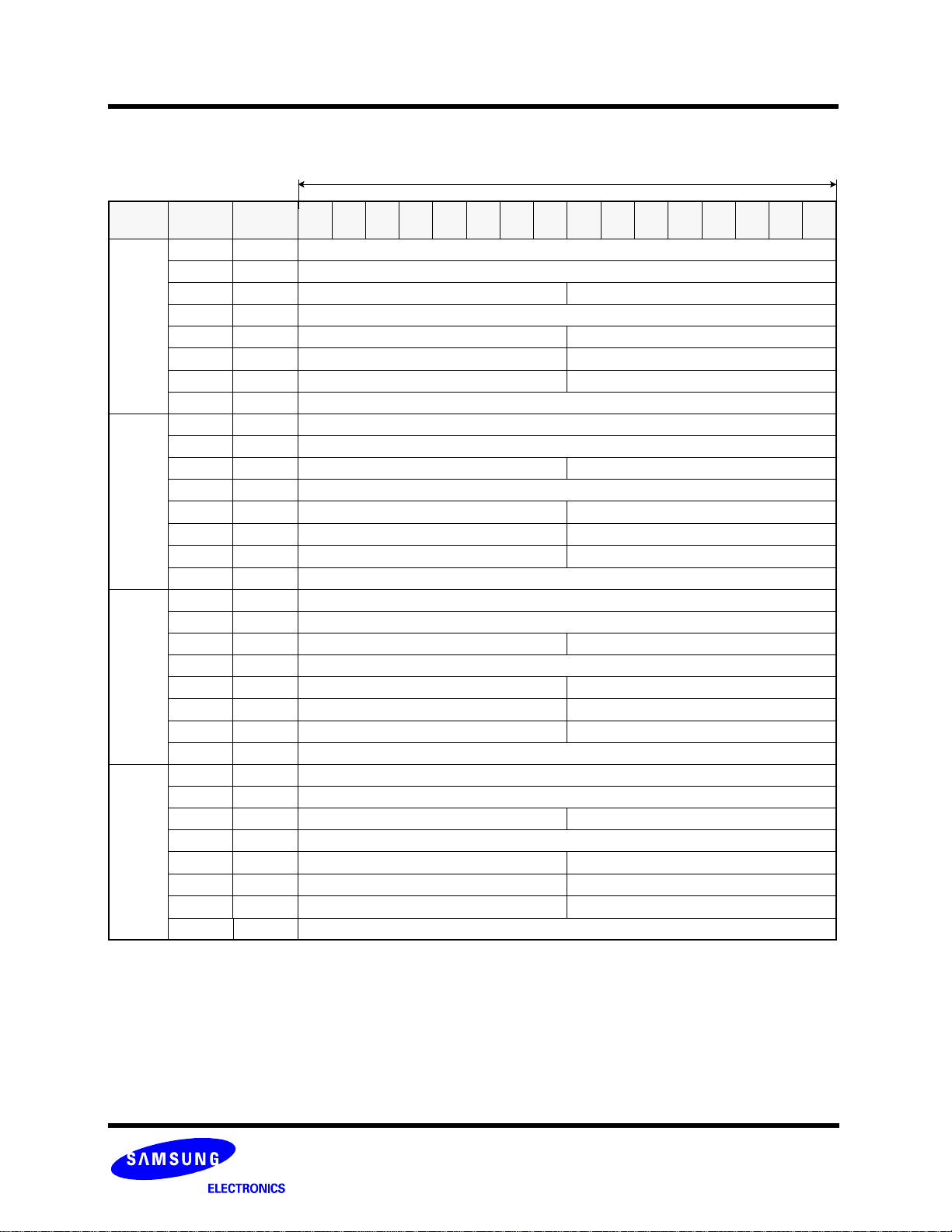
7. Detailed address map for registers
Address
(word order)
F000h 1E000h Manufacturer ID R Manufacturer identification
F001h 1E002h Device ID R Device identification
F002h 1E004h Version ID R Version identification
F003h 1E006h Data Buffer size R Data buffer size
F004h 1E008h Boot Buffer size R Boot buffer size
F005h 1E00Ah
F006h 1E00Ch Technology R Info about technology
F007h~F0FFh 1E00Eh~1E1FEh Reserved - Reserved for User
F100h 1E200h Start address 1 R/W NAND Flash Block address
F101h 1E202h Start address 2 R/W Reserved
F102h 1E204h Start address 3 R/W Destination Block address for Copy back program
F103h 1E206h Start address 4 R/W
F104h 1E208h Start address 5 - N/A
F105h 1E20Ah Start address 6 - N/A
F106h 1E20Ch Start address 7 - N/A
F107h 1E20Eh Start address 8 R/W NAND Flash Page & Sector address
F108h~F1FFh 1E210h~1E3FEh Reserved - Reserved for User
F200h 1E400h Start Buffer R/W
F201h~F207h 1E402h~1E40Eh Reserved - Reserved for User
F208h~F21Fh 1E410h~1E43Eh Reserved - Reserved for vendor specific purposes
F220h 1E440h Command R/W Host control and memory operation commands
F221h 1E442h
F222h 1E444h
F223h~F22Fh 1E446h~1E45Eh Reserved - Reserved for User
F230h~F23Fh 1E460h~1E47Eh Reserved - Reserved for vendor specific purposes
F240h 1E480h Controller Status R Controller Status and result of memory operation
F241h 1E482h Interrupt R/W Memory Command Completion Interrupt Status
F242h~F24Bh 1E484h~1E496h Reserved - Reserved for User
F24Ch 1E498h
F24Dh 1E49Ah
F24Eh 1E49Ch
F24Fh~FEFFh 1E49Eh~1FDFEh Reserved - Reserved for User
Address
(byte order)
Name
Amount of
buffers
System
Configuration 1
System
Configuration 2
Unlock Start
Block Address
Unlock End
Block Address
Write Protection
Status
Host
Access
R Amount of data/boot buffers
Destination Page & Sector address for Copy
back program
Number Buffer of for the page data transfer to/from the
memory and the start Buffer Address
The meaning is with which buffer to start and how many
buffers to use for the data transfer
R, R/W Memory and Host Interface Configuration
-N/A
Start memory block address to unlock in Write
R/W
Protection mode
End memory block address to unlock in Write
R/W
Protection mode
Current memory Write Protection status
R
(unlocked/locked/tight-locked)
Description
19
Page 20
OneNAND128 FLASH MEMORY
Address
(word order)
FF00h 1FE00h
FF01h 1FE02h
FF02h 1FE04h
FF03h 1FE06h
FF04h 1FE08h
FF05h~FFFFh 1FE12h~1FF0Ah Reserved - Reserved for vendor specific purposes
Address
(byte order)
Name
ECC Status
Register
ECC Result of
main area data
ECC Result of
spare area data
ECC Result of
main area data
ECC Result of
spare area data
Host
Access
R ECC status of sector
ECC error position of Main area data error for first
R
selected Sector
ECC error position of Spare area data error for first
R
selected Sector
ECC error position of Main area data error for second
R
selected Sector
ECC error position of Spare area data error for second
R
selected Sector
Description
20
Page 21
OneNAND128 FLASH MEMORY
7. Address Register (word order)
7.1 Manufacturer ID Register (R): F000h, default=00ECh
15 14 13 12 11 10 9 8 7 6 5 4 3 2 1 0
ManufID
ManufID (Manufacturer ID): manufacturer identification, 00ECh for Samsung Electronics Corp.
7.2 Device ID Register (R): F001h, default=refer to Table1
15 14 13 12 11 10 9 8 7 6 5 4 3 2 1 0
DeviceID
DeviceID (Device ID): Device Identification,
Table 1.
Device DeviceID[15:0]
KFG2816Q1M 0004h
KFG2816D1M 0005h
KFG2816U1M 0005h
7.3 Version ID Register (R): F002h
: N/A
21
Page 22
OneNAND128 FLASH MEMORY
7.4 Data Buffer size Register(R): F003h, default=0400h
15 14 13 12 11 10 9 8 7 6 5 4 3 2 1 0
DataBufSize
DataBufSize: total data buffer size in words in the memory interface used for shrinks
Equals two buffers of 512 words each(2x512=2
7.5 Boot Buffer size Register (R): F004h, default=0200h
15 14 13 12 11 10 9 8 7 6 5 4 3 2 1 0
BootBufSize: total boot buffer size in words in the memory interface
(512 words=2
9
, N=9)
7.6 Amount of Buffers Register (R): F005h, default=0201h
15 14 13 12 11 10 9 8 7 6 5 4 3 2 1 0
DataBufAmount BootBufAmount
DataBufAmount: the amount of data buffer=2(2N, N=1)
BootBufAmount: the amount of boot buffer=1(2
7.7 Technology Register (R): F006h, default=0000h
15 14 13 12 11 10 9 8 7 6 5 4 3 2 1 0
Tech: technology information, what technology is used for the memory
N
N
, N=0)
, N=10)
BootBufSize
Te ch
Tech Technology
0000h NAND SLC
0001h NAND MLC
0002h-FFFFh Reserved
22
Page 23
OneNAND128 FLASH MEMORY
7.8 Start Address1 Register (R/W): F100h, default=0000h
15 14 13 12 11 10 9 8 7 6 5 4 3 2 1 0
Reserved(00000000) FBA
FBA (NAND Flash Block Address): NAND Flash block address which will be read or programmed or erased.
Device Number of Block FBA
128Mb 256 FBA[7:0]
7.9 Start Address2 Register (R/W): F101h, default=0000h
15 14 13 12 11 10 9 8 7 6 5 4 3 2 1 0
Reserved(0000000000000000)
7.10 Start Address3 Register (R/W): F102h, default=0000h
15 14 13 12 11 10 9 8 7 6 5 4 3 2 1 0
Reserved(00000000) FCBA
FCBA (NAND Flash Copy Back Block Address): NAND Flash destination block address which will be copy back programmed.
Device Number of Block FBA
128Mb 256 FBA[7:0]
7.11 Start Address4 Register (R/W): F103h, default=0000h
15 14 13 12 11 10 9 8 7 6 5 4 3 2 1 0
Reserved(00000000) FCPA Reserved FCSA
FCPA (NAND Flash Copy Back Page Address): NAND Flash destination page address in a block for copy back program operation.
FCPA(default value) = 000000
FCPA range : 000000~111111, 6bits for 64 pages
FCSA (NAND Flash Copy Back Sector Address): NAND Flash destination sector address in a page for copy back program operation.
FCSA(default value) = 0
FCSA range : 0~1, 1bits for 2 sectors
23
Page 24
OneNAND128 FLASH MEMORY
7.12 Start Address5 Register: F104h
: N/A
7.13 Start Address6 Register: F105h
: N/A
7.14 Start Address7 Register: F106h
: N/A
7.15 Start Address8 Register (R/W): F107h, default=0000h
15 14 13 12 11 10 9 8 7 6 5 4 3 2 1 0
Reserved (00000000) FPA Reserved FSA
FPA (NAND Flash Page Address): NAND Flash start page address in a block for page read or copy back program or program operation.
FPA(default value)=000000
FPA range: 000000~111111 , 6bits for 64 pages
FSA (Flash Sector Address): NAND Flash start sector address in a page for read or copy back program or program operation.
FSA(default value) = 0
FSA range : 0~1, 1bits for 2 sectors
7.16 Start Buffer Register (R/W): F200h, default=0000h
15 14 13 12 11 10 9 8 7 6 5 4 3 2 1 0
Reserved(0000) BSA Reserved(0000000) BSC
BSC (BufferRAM Sector Count): this field specifies the number of sectors to be read or programmed or copy back programmed.
Its maximum count is 2 sectors at 0(default value)value.
For a single sector access, it should be programmed as value 1 and it should be programmed as value 0 for two sectors.
However internal RAM buffer reached to 1 value(max. value), it counts up to 0 value to satisfy BSC value.
for example) if BSA=1101, BSC=0, then selected BufferRAM are ’1101->1100’.
BSA (BufferRAM Sector Address): It is the place where data is placed and specifies the sector 0~1 in the internal BootRAM and DataRAM.
BSA[3] is the selection bit between BootRAM and DataRAM.
BSA[2] is the selection bit between DataRAM0 and DataRAM1.
BSA[0] is the selection bit between Sector0 and Sector1 in the internal BootRAM and DataRAM.
While one of BootRAM or DataRAM0 interfaces with memory, the other RAM is inaccessible.
BootRAM
DataRAM0
DataRAM1
Main area data
{
BootRAM 0
BootRAM 1
DataRAM 0_0
DataRAM 0_1
DataRAM 1_0
DataRAM 1_1
Spare area data
{
BSA
0000
0001
1000
1001
1100
1101
24
Sector: (512 + 16)byte
BSC Number of Sectors
1 1 sector
0 2 sectors
Page 25
OneNAND128 FLASH MEMORY
7.17 Command Register (R/W): F220h, default=0000h
15 14 13 12 11 10 9 8 7 6 5 4 3 2 1 0
Command
Command: operation of the memory interface
Acceptable
CMD Operation
0000h Load single/multiple sector data unit into buffer 00F0h, 00F3h
0013h Load single/multiple spare sector into buffer 00F0h, 00F3h
0080h Program single/multiple sector data unit from buffer 00F0h, 00F3h
001Ah Program single/multiple spare area sector from buffer 00F0h, 00F3h
001Bh Copy back program 00F0h, 00F3h
0023h Unlock NAND array block(s) from start block address to end block address -
002Ah Lock NAND array block(s) from start block address to end block address -
002Ch Lock-tight NAND array block(s) from start block address to end block address -
0071h Erase Verify Read 00F0h, 00F3h
0094h Block Erase 00F0h, 00F3h
0095h Multi-Block Erase 00F0h, 00F3h
00B0h Erase Suspend 00F3h
0030h Erase Resume 00F0h, 00F3h
00F0h Reset NAND Flash Core -
00F3h Reset OneNAND 1) -
0065h OTP Access 00F0h, 00F3h
NOTE:
1)’Reset OneNAND’(=Hot reset) command makes the registers(except RDYpol, INTpol, IOBE, and OTP
the warm reset(=reset by RP
pin).
L bits) and NAND Flash core into default state as
command
during busy
This R/W register describes the operation of the OneNAND interface.
Note that all commands should be issued right after INT is turned from ready state to busy state. (i.e. right after 0 is written to INT register.) After any
command is issued and the corresponding operation is completed, INT goes back to ready state. (00F0h and 00F3h may be accepted during busy state
of some operations. Refer to the rightmost column of the command register table above.)
25
Page 26
OneNAND128 FLASH MEMORY
7.18 System Configuration 1 Register (R, R/W): F221h, default=40C0h
15 14 13 12 11 10 9 8 7 6 5 4 3 2 1 0
R/W R/W R/W R/W R/W R/W R/W R R
RM BRL BL ECC
RM (Read Mode): this field specifies the selection between asynchronous read mode and synchronous read mode
RDY
pol
INT
pol
IOB
E
RM Read Mode
0 Asynchronous read(default)
1 Synchronous read
BRL (Burst Read Latency): this field specifies the initial access latency in the burst read transfer.
BRL Latency Cycles
000 8(N/A)
001 9(N/A)
010 10(N/A)
011 3(up to 40MHz)
100 4(default, min.)
101 5
110 6
111 7
Reserved(0000)
BW
PS
BL (Burst Length): this field specifies the size of burst length during Sync. burst read. Wrap around and linear burst.
BL Burst Length(Main) Burst Length(Spare)
000 Continuous(default)
001 4 words
010 8 words
011 16 words
100 32 words N/A
101~111 Reserved
ECC: Error Correction Operation,
0=with correction(default), 1=without correction(by-passed)
RDYpol: RDY signal polarity
0=low for ready, 1=high for ready((default)
INTpol: INT Pin polarity
0=low for Interrupt pending , 1=high for Interrupt pending (default)
INTpol INT bit of Interrupt Status Register INT Pin output
00 1
10 0
IOBE: I/O buffer enable for INT and RDY signals, INT and RDY outputs are HighZ at power-up, bit 7 and 6 become valid after IOBE is set to1. IOBE can
be reset only by Cold reset or by writing 0 to bit 5 of System Configuration 1 register.
0=disable(default), 1=enable
BWPS: boot buffer write protect status,
0=locked(fixed)
26
Page 27
OneNAND128 FLASH MEMORY
7.19 System Configuration 2 Register : F222h
: N/A
7.22 Controller Status Register (R): F240h, default=0000h
15 14 13 12 11 10 9 8 7 6 5 4 3 2 1 0
OnGo Lock Load Prog Erase Error Sus PRp RSTB OTP
OnGo: this bit shows the overall internal status of OneNAND
0=ready, 1=busy
Lock: this bit shows whether host loads data from NAND Flash array into locked BootRAM or programs/erases locked block of NAND Flash array.
L Reserved(000000)
Lock Locked/Unlocked Check Result
0 Unlocked
1 Locked
Error (Current Sector/Page Write Result): this bit shows current sector/page Load/Program/Copy Back Program/Erase result of flash memory or whether
host puts invalid command into the device.
TO
(0)
Error
Current Sector/Page Load/Program/CopyBack. Program/Erase Result
and Invalid Command Input
0Pass
1Fail
Sus (Erase Suspend/Resume):this bit shows the Erase Suspend Status.
Sus Erase Suspend Status
0 Erase Resume(Default)
1 Erase Suspend
OTPL (OTP Lock Status):this bit shows OTP block is locked or unlocked. OTPL bit is automatically updated at power-on.
OTPL OTP Locked/Unlocked Status
0 OTP Block Unlock Status(Default)
1 OTP Block Lock Status(Disable OTP Program/Erase)
TO (Time Out): time out for read/program/copy back program/erase
0=no time out(fixed)
Load : this bit shows the Load operation status
0=ready(default), 1=busy or error case, refer to the table 3
Prog (Program Busy) : this bit shows the Program operation status
0=ready(default), 1=busy or error case, refer to the table 3
Erase (Erase Busy) : this bit shows the Erase operation status
0=ready(default), 1=busy or error case, refer to the table 3
RSTB (Reset Busy) : this bit shows the Reset operation status
0=ready(default), 1=busy or error case, refer to the table 3
27
Page 28

OneNAND128 FLASH MEMORY
Table 3. Controller Status Register output for modes.
Mode
OnGo Lock Load Prog Erase Error Sus Reserved(0) RSTB OTPL Reserved(0) TO
Load Ongoing 1 0 1 0 0 0 0 0 0 0/1 00000 0
Program Ongoing 1 0 0 1 0 0 0 0 0 0/1 00000 0
Erase Ongoing 1 0 0 0 1 0 0 0 0 0/1 00000 0
Reset Ongoing 1 0 0 0 0 0 0 0 1 0/1 00000 0
Multi-Block Erase
Ongoing
Erase Verify Read
Ongoing
1 0 0 0 1 0 0 0 0 0/1 00000 0
1 0 0 0 0 0 0 0 0 0/1 00000 0
Load OK 0 0 0 0 0 0 0 0 0 0/1 00000 0
Program OK 0 0 0 0 0 0 0 0 0 0/1 00000 0
Erase OK 0 0 0 0 0 0 0 0 0 0/1 00000 0
Erase Verify Read
3)
OK
Load Fail
1)
0 0 0 0 0 0 0 0 0 0/1 00000 0
0 0 1 0 0 1 0 0 0 0/1 00000 0
Program Fail 0 0 0 1 0 1 0 0 0 0/1 00000 0
Erase Fail 0 0 0 0 1 1 0 0 0 0/1 00000 0
Erase Verify Read
3)
Fail
Load Reset
2)
0 0 0 0 1 1 0 0 0 0/1 00000 0
0 0 1 0 0 1 0 0 1 0/1 00000 0
Program Reset 0 0 0 1 0 1 0 0 1 0/1 00000 0
Erase Reset 0 0 0 0 1 1 0 0 1 0/1 00000 0
Erase Suspend 0 0 0 0 1 0 1 0 0 0/1 00000 0
Program Lock 0 1 0 1 0 1 0 0 0 0/1 00000 0
Erase Lock 0 1 0 0 1 1 0 0 0 0/1 00000 0
Load Lock(Buffer Lock) 0 1 1 0 0 1 0 0 0 0/1 00000 0
OTP Program
Fail(Lock)
0 1 0 1 0 1 0 0 0 1 00000 0
OTP Program Fail 0 0 0 1 0 1 0 0 0 0 00000 0
OTP Erase Fail 0 1 0 0 1 1 0 0 0 0/1 00000 0
Program Ongo-
ing(Susp.)
1 0 0 1 1 0 1 0 0 0/1 00000 0
Load Ongoing(Susp.) 1 0 1 0 1 0 1 0 0 0/1 00000 0
Program Fail(Susp.) 0 0 0 1 1 1 1 0 0 0/1 00000 0
Load Fail(Susp.) 0 0 1 0 1 1 1 0 0 0/1 00000 0
Invalid Command 0 0 0 0 0 1 0 0 0 0/1 00000 0
Invalid Command(Susp.)
NOTE:
1. ERm and/or ERs bits in ECC status register at Load Fail case is 10. (2bits error - uncorrectable)
2. ERm and ERs bits in ECC status register at Load Reset case are 00. (No error)
3. Multi Block Erase status should be checked by Erase Verify Read operation.
4. OTP Erase does not update the register and the previous value is kept.
0 0 0 0 1 1 1 0 0 0/1 00000 0
Controller Status Register [15:0]
28
Page 29

OneNAND128 FLASH MEMORY
7.23 Interrupt Status Register (R/W): F241h, default=8080h(after Cold reset),8010h(after Warm/Hot reset)
15 14 13 12 11 10 9 8 7 6 5 4 3 2 1 0
INT Reserved(0000000) RI WI EI RSTI Reserved(0000)
Bit
Address
15 INT(interrupt): the master interrupt bit 1 1 0 Interrupt Off
- Set to ’1’ of itself when one or more of RI, WI, EI and
RSTI is set to ’1’, or Unlock(0023h), Lock(002Ah), Lock tight(002Ch), or Erase Verify Read(0071h), or OTP
access(0065h) operation, or "Load Data into Buffer" is
completed.
- Cleared to ’0’ when by writing ’0’ to this bit or by
reset(Cold/Warm/Hot reset).
’0’ in this bit means that INT pin is low status.
(This INT bit is directly wired to the INT pin on the chip.
INT pin goes low upon writing ’0’ to this bit when
INTpol is high and goes high upon writing ’0’ to this
bit when INTpol is low. )
7 RI(Read Interrupt): 1 0 0 Interrupt Off
- Set to ’1’ of itself at the completion of Load Operation
(0000h, 0013h, or boot is done.)
- Cleared to ’0’ when by writing ’0’ to this bit or by reset
(Cold/Warm/Hot reset).
6 WI(Write Interrupt): 0 0 0 Interrupt Off
- Set to ’1’ of itself at the completion of Program Operation
(0080h, 001Ah, or 001Bh)
- Cleared to ’0’ when by writing ’0’ to this bit or by reset
(Cold/Warm/Hot reset).
5 EI(Erase Interrupt): 0 0 0 Interrupt Off
- Set to ’1’ of itself at the completion of Erase Operation
(0094h, 0095h, or 0030h)
- Cleared to ’0’ when by writing ’0’ to this bit or by reset
(Cold/Warm/Hot reset).
4 RSTI(Reset Interrupt): 0 1 0 Interrupt Off
- Set to ’1’ of itself at the completion of Reset Operation
(00B0h, 00F0h, 00F3h, or warm reset is released.)
- Cleared to ’0’ when by writing ’0’ to this bit.
Bit Name Default State Valid
Cold Warm/Hot
States
0->1 Interrupt Pending
0->1 Interrupt Pending
0->1 Interrupt Pending
0->1 Interrupt Pending
0->1 Interrupt Pending
Function
7.24 Start Block Address (R/W): F24Ch, default=0000h
15 14 13 12 11 10 9 8 7 6 5 4 3 2 1 0
Reserved(00000000) SBA
SBA (Lock/Unlock/Lock-tight Start Block Address): Start NAND Flash block address in Write Protection mode, which follows ’Lock block command’ or
’Unlock block command’ or ’Lock-tight command’.
7.25 End Block Address (R/W): F24Dh, default=0000h
15 14 13 12 11 10 9 8 7 6 5 4 3 2 1 0
Reserved(00000000) EBA
EBA (Lock/Unlock/Lock-tight End Block Address): End NAND Flash block address in Write Protection mode, which follows ’Lock block command’ or
’Unlock block command’ or ’Lock-tight command’. EBA should be equal to or larger than SBA.
Device Number of Block SBA/EBA
128Mb 256 [7:0]
29
Page 30

OneNAND128 FLASH MEMORY
7.26 NAND Flash Write Protection Status (R): F24Eh, default=0002h
15 14 13 12 11 10 9 8 7 6 5 4 3 2 1 0
Reserved(0000000000000) US LS LTS
US (Unlocked Status): ’1’ value of this bit specifies that the current block in NAND Flash is unlocked.
LS (Locked Status): ’1’ value of this bit specifies that the current block in NAND Flash is in locked status.
LTS (Lock-tighten Status): ’1’ value of this bit specifies that current block in NAND Flash is lock-tighten.
7.27 ECC Status Register(R): FF00h, default=0000h
15 14 13 12 11 10 9 8 7 6 5 4 3 2 1 0
Reserved(00000000) ERm1 ERs1 ERm0 ERs0
ERm (ECC Error for Main area data) & ERs (ECC Error for Spare area data)
: ERm0/1 is for first/second selected sector in main of BufferRAM, ERs0/1 is for first/second selected sector in spare of
BufferRAM.
ERm and ERs show the number of error nits in a sector as a result of ECC check at the load operation.
ERm, ERs ECC Status
00 No Error
01 1-bit error(correctable)
10
11 R eserve d
NOTE:
1. 3bits or more error detection is not supported.
2-bit error(uncorrectable)
7.28 ECC Result of first selected Sector Main area data Register (R): FF01h, default=0000h
15 14 13 12 11 10 9 8 7 6 5 4 3 2 1 0
Reserved(0000) ECCposWord0 ECCposIO0
1)
7.29 ECC Result of first selected Sector Spare area data Register (R): FF02h, default=0000h
15 14 13 12 11 10 9 8 7 6 5 4 3 2 1 0
Reserved(0000000000) ECClogSector0 ECCposIO0
7.30 ECC Result of second selected Sector Main area data Register (R): FF03h, default=0000h
15 14 13 12 11 10 9 8 7 6 5 4 3 2 1 0
Reserved(0000) ECCposWord1 ECCposIO1
7.31 ECC Result of second selected Sector Spare area data Register (R): FF04h, default=0000h
15 14 13 12 11 10 9 8 7 6 5 4 3 2 1 0
Reserved(0000000000) ECClogSector1 ECCposIO1
NOTE:
1. ECCposWord: ECC error position address that selects one of Main area data(256words)
2. ECCposIO: ECC error position address which selects one of sixteen DQs (DQ 0~DQ 15).
3. ECClogSector: ECC error position address that selects one of the 2nd word and LSB of the 3rd word of spare area. Refer to the below table.
ECClogSector Information [5:4]
ECClogSector Error Position
00 2nd word
01 3rd word
10, 11 Reserved
4. ECCposWord, ECCposIO and ECClogSector are updated in boot loading operation, too.
30
Page 31

OneNAND128 FLASH MEMORY
8. Device Operation
The device supports both a limited command based and a register based interface for performing operations on the device, reading
device ID, writing data to buffer etc. The command based interface is active in the boot partition, i.e. commands can only be written
with a boot area address. Boot area data is only returned if no command has been issued prior to the read.
8.1 Command based operation
The entire address range, except for the boot area, can be used for the data buffer. All commands are written to the boot partition. Writes outside the
boot partition are treated as normal writes to the buffers or registers. The command consists of one or more cycles depending on the command. After
completion of the command the device starts its execution. Writing incorrect information which include address and data or writing an improper command
will terminate the previous command sequence and make the device go to the ready status. The defined valid command sequences are stated in Table4.
Table 4. Command Sequences
Command Definition Cycles 1st cycle 2nd cycle
Read Data from Buffer
Write Data to Buffer
Reset OneNAND
Load Data into Buffer
Read Identification Data
NOTE:
1) DP(Data Partition) : DataRAM Area
2) BP(Boot Partition) : BootRAM Area [0000h ~ 01FFh, 8000h ~ 800Fh].
3) Load Data into Buffer operation is available within a block(64KB)
4) Load 1KB unit into DataRAM0. Current Start address(FPA) is automatically incremented by 1KB unit after the load.
5) 0000h -> Data is Manufacturer ID
0001h -> Data is Device ID
0002h -> Current Block Write Protection Status
toggling can terminate ’Read Identification Data’ operation.
6) WE
3)
6)
Add
Data Data
Add
Data Data
Add
Data 00F0h
Add
Data 00E0h
Add
Data 0090h Data
1
1
1
2
2
1)
DP
DP
2)
BP
BP BP
0000h
BP
XXXXh
4)
5)
8.1.1 Read Data from Buffer
Buffer can be read by addressing a read to a wanted buffer area
8.1.2 Write Data to Buffer
Buffer can be written by addressing a write to a wanted buffer area
8.1.3 Reset OneNAND
Reset command is given by writing 00F0h to the boot partition address. Reset will return all default values into the device.
8.1.4 Load Data into Buffer
Load Data into Buffer command is a two-cycle command. Two sequential designated command activates this operation. Sequentially writing 00E0h
and 0000h to the boot partition [0000h~01FFh, 8000h~800Fh] will load one page to DataRAM0. This operation refers to FBA and FPA. FSA, BSA, and
BSC are not considered.
At the end of this operation, FPA will be automatically increased by 1. So continuous issue of this command will sequentially load data in next page to
DataRAM0. This page address increment is restricted within a block.
The default value of FBA and FPA is 0. Therefore, initial issue of this command after power on will load the first page of memory, which is usually boot
code.
8.1.5 Read Identification Data
Read Identification Data command consists of two cycles. It gives out the devices identification data according to the given address. The first cycle is
0090h to the boot partition address and second cycle is read from the addresses specified in Table5.
31
Page 32

OneNAND128 FLASH MEMORY
Table 5. Identification data description
Address Data Out
0000h Manufacturer ID 00ECh
0001h Device ID refer to table 1
0002h Current Block Write Protection Status
8.2 Device Bus Operations
Operation CE OE WE ADD0~15 DQ0~15 RP CLK AV D
Standby H X X X High-Z H X X
Warm Reset XXXXHigh-ZL XX
Asynchronous Write L H L Add. In Data In H L
Asynchronous Read L L H Add. In Data Out H L
Load Initial Burst Address L H H Add. In X H
refer to NAND Flash Write Protection Status Register
Burst Read L L H X
Terminate Burst Read
Cycle
Terminate Burst Read
Cycle via RP
Terminate Current Burst
Read Cycle and Start
New Burst Read Cycle
Note : L=VIL (Low), H=VIH (High), X=Don’t Care.
HXHXHigh-ZHXX
XXXXHigh-ZLXX
Burst Data
Out
H H Add In High-Z H
H
X
32
Page 33

OneNAND128 FLASH MEMORY
8.3 Reset Mode
Cold Reset
At system power-up, the voltage detector in the device detects the rising edge of Vcc and releases internal power-up reset signal
which triggers bootcode loading. Bootcode loading means that the boot loader in the device copies designated sized data(1KB) from
the beginning of memory to the BootRAM.
POR triggering level
System Power
OneNAND
Operation
1)
Sleep Bootcode copy Idle
Bootcode - copy done
2)
RP
INT
INT bit
IOBE bit
INTpol bit
Note: 1) Bootcode copy operation starts 400us later than POR activation.
The system power should reach 1.7V after POR triggering level(typ. 1.5V) within 400us for valid boot code data.
2) 1K bytes Bootcode copy takes 70us(estimated) from sector0 and sector1/page0/block0 of NAND Flash array to BootRAM.
Host can read Bootcode in BootRAM(1K bytes) after Bootcode copy completion.
3) INT register goes ‘Low’ to ‘High’ on the condition of ‘Bootcode-copy done’ and RP
If RP
goes ‘Low’ to ‘High’ before ‘Bootcode-copy done’, INT register goes to ‘Low’ to ‘High’ as soon as ‘Bootcode-copy done’
High-Z
0 (default)
0 (default)
1 (default)
rising edge.
3)
1
1
Figure 5. Cold Reset Timings
33
Page 34

OneNAND128 FLASH MEMORY
Warm Reset
Warm reset means that the host resets the device by RP pin, and then the device stops all logic current operation and executes internal reset operation(Note 1) synchronized with the falling edge of RP
the rising edge of RP
reset operation in case RP
contents of memory cells being altered are no longer valid as the data will be partially programmed or erased. Warm reset has no
effect on contents of BootRAM and DataRAM.
CE, OE
. The device logic will not be reset in case RP pulses shorter than 200ns, but the device guarantees the logic
pulse is longer than 200ns. NAND Flash core reset will abort current NAND Flash Core operation. The
RP
and resets current NAND Flash core operation synchronized with
MuxOneNAND
Operation
INT
RDY
initiated by RP
Operation or Idle
High-Z High-Z High-Z
internal reset operation
low
NAND Flash core reset
initiated by RP
high
Idle
Operation
Figure 6. Warm Reset Timings
Operation or Idle
34
Page 35

OneNAND128 FLASH MEMORY
Hot Reset
Hot reset means that the host resets the device by reset command(Note 2), and then the device logic stops all current operation and
executes internal reset operation(Note 1) , and resets current NAND Flash core operation. Hot reset has no effect on contents of
BootRAM and DataRAM.
AVD
A0~A15
DQ0~DQ15
BP(Note 3)
or F220h
00F0h
or 00F3h
CE
WE
INT
RDY
OneNAND
Operation
High-Z
Operation or Idle OneNAND reset
Idle
Figure 7. Hot Reset Timings
NOTE:
1. Internal reset operation means that the device initializes internal registers and makes output signals go to default status and bufferRAM data are kept
unchanged after Warm/Hot reset operations.
2. Reset command : Command based reset or Register based reset
3. BP(Boot Partition) : BootRAM area[0000h~01FFh, 8000h~800Fh]
35
Page 36

OneNAND128 FLASH MEMORY
NAND Flash Core Reset
Host can reset NAND Flash Core operation by NAND Flash Core reset command. NAND Flash Core Reset will abort the current
NAND Flash core operation. During a NAND Flash Core Reset, the content of memory cellls being altered is no longer valid as the
data will be partially programmed or erased. NAND Flash Core Reset has an effect on neither contents of BootRAM and DataRAM
nor register values.
AVD
A0~A15
DQ0~DQ15
CE
WE
INT
RDY
OneNAND
Operation
F220h
00F0h
High-Z
Operation or Idle NAND Flash Core reset
Figure 8. NAND Flash Core Reset Timings
Idle
36
Page 37

OneNAND128 FLASH MEMORY
Table 6. Internal Register reset
Hot
Reset
(00F3h)
Internal Registers Default Cold Reset
Warm Reset
(RP
)
F000h Manufacturer ID Register (R) 00ECh N/A N/A N/A N/A
F001h Device ID Register (R) Note3 N/A N/A N/A N/A
F002h Version ID Register (rR) - N/A N/A N/A N/A
F003h Data Buffer size Register (R) 0400h N/A N/A N/A N/A
F004h Boot Buffer size Register (R) 0200h N/A N/A N/A N/A
F005h Amount of Buffers Register (R) 0201h N/A N/A N/A N/A
F006h Technology Register (R) 0000h N/A N/A N/A N/A
F100h Start Address1 Register (R/W): FBA 0000h 0000h 0000h 0000h N/A
F101h Start Address2 Register (R/W): Reserved 0000h 0000h 0000h 0000h N/A
F102h Start Address3 Register (R/W): FCBA 0000h 0000h 0000h 0000h N/A
F103h Start Address4 Register (R/W): FCPA, FCSA 0000h 0000h 0000h 0000h N/A
F107h Start Address8 Register (R/W): FPA, FSA 0000h 0000h 0000h 0000h N/A
F200h Start Buffer Register (R/W): BSA, BSC 0000h 0000h 0000h 0000h N/A
F220h Command Register (R/W) 0000h 0000h 0000h 0000h N/A
F221h System Configuration 1 Register (R/W) 40C0h 40C0h O
(Note1) O (Note1) N/A
F240h Controller Status Register (R) 0000h 0000h 0000h 0000h N/A
F241h Interrupt Status Register (R/W) - 8080h 8010h 8010h N/A
F24Ch Lock/Unlock Start Block Address (R/W) 0000h 0000h 0000h N/A N/A
F24Dh Lock/Unlock End Block Address (R/W) 0000h 0000h 0000h N/A N/A
F24Eh NAND Flash Write Protection Status (R) 0002h 0002h 0002h N/A N/A
FF00h ECC Status Register (R) (Note2) 0000h 0000h 0000h 0000h N/A
FF01h
FF02h
FF03h
FF04h
ECC Result of Sector 0 Main area data Register(R)
ECC Result of Sector 0 Spare area data Register (R)
ECC Result of Sector 1 Main area data Register(R)
ECC Result of Sector 1 Spare area data Register (R)
0000h 0000h 0000h 0000h N/A
0000h 0000h 0000h 0000h N/A
0000h 0000h 0000h 0000h N/A
0000h 0000h 0000h 0000h N/A
Hot
Reset
(BP-F0)
NAND Flash
Reset(00F0h)
NOTE: 1) RDYpol, INTpol, and IOBE are reset by Cold reset. The other bits are reset by Cold/Warm/Hot reset.
OTP
2) ECC Status Register & ECC Result Registers are reset when any command is issued.
3) Refer to table 1
L is not reset but updated by Cold reset.
37
Page 38

OneNAND128 FLASH MEMORY
Write Protection
Write Protection for BootRAM
At system power-up, the voltage detector in the device detects the rising edge of Vcc and releases the internal power-up reset signal
which triggers bootcode loading. And the designated size data(1KB) is copied from the beginning of the memory to the BootRAM.
After the bootcode loading is completed, the BootRAM is always locked to protect the significant boot code from accidental write.
Write Protection for NAND Flash array
Write Protection Modes
The device offers both hardware and software write protection features for NAND Flash array. The software write protection feature is
used by writing Lock command or Lock-tight command to command register; The 002Ah or 002Ch command is written into F220h
register. The partial write protection feature is also permitted by writing Partial Lock(002Ah) and Partial Lock-Tight(002Ch) command
with the start address and the end address to F24Ch and F24Dh registers. The hardware write protection feature is used by executing
cold or warm reset. The default state is locked, and all NAND Flash array goes to locked state after cold or warm reset.
Write Protection Commands
Individual or consecutive instant secured block protects code and data by allowing any block to be locked or lock-tighten. The write
protection scheme offers two levels of protection. The first allows software-only control of write protection(useful for frequently
changed data blocks), while the second requires hardware interaction before locking can be changed(protects infrequently changed
code blocks).
The following summarize the locking functionality.
> All blocks power-up in a locked state. Unlock command can unlock these blocks with the start and end block address.
> Partial Lock-Tight command makes the part of locked block(s) to be lock-tightened by writing the start and end block address. And
lock-tightened state can be returned to lock state only when cold or warm reset is asserted.
> Only one individual area can be lock-tightened by Partial Lock-tight command; i.e lock-tightening multi area is not available.
> Lock-tightened blocks offer the user an additional level of write protection beyond that of a regular locked block. Lock-tightened
block can’t have it’s state changed by software, it can be changed by warm reset or cold reset.
> Unlock start or end block address is reflected immediately to the device only when Unlock command is issued, and NAND Flash
write protection status register is also updated at that time.
> Unlocked blocks can be programmed or erased.
> Only one area can be released from lock state to unlock state with Unlock command and addresses. This unlocked area can be
changed with new Unlock command; when new Unlock command is issued, last unlocked area is locked again and new area is
unlocked.
> Partial Lock command makes the part of unlocked block(s) to be locked with the start and end block address.
> Only one area can be locked with Partial Lock command and address. This locked area can be changed with new Partial Lock command; when new Partial Lock command is issued, last unlocked area is locked again and new area is unlocked.
Write Protection Status
The block current Write Protection status can be read in NAND Flash Write Protection Status Register(F24Eh). There are three bits US, LS, LTS -, which are not cleared by hot reset. These Write Protection status registers are updated when Write Protection command is entered.
The followings summarize locking status.
example)
In default, [2:0] values are 010.
-> If host executes unlock block operation, then [2:0] values turn to 100.
-> If host executes lock-tight block operation, then [2:0] values turn to 001.
38
Page 39

OneNAND128 FLASH MEMORY
Locked
> Command Sequence :
Start block address+End block address+Lock block command
(002Ah)
> All blocks default to be locked after Cold reset or Warm reset
> Unlocked blocks can be locked by using the Lock block
command and a lock block’s status can be changed to
unlock or lock-tight using the appropriate software commands
Unlocked
> Command Sequence :
Start block address+End block address+Unlock block command
(0023h)
> Unlocked block can be programmed or erased
> An unlocked block’s status can be changed to the locked or
lock-tighten state using the appropriate software command
> Only one sequential area can be released to unlock state from
lock state ; Unlocking multi individual area is not available
Lock-tighten
> Command Sequence :
Start block address+End block address+Lock-tight block command
(002Ch)
> Lock-tighten blocks offer the user an additional level of write
:
protection beyond that of a regular lock block. A block that
is lock-tighten cannot have its state change by software,
only by Cold or Warm reset.
> Only locked blocks can be lock-tighten by Lock-tight command.
> Lock-tighten blocks revert to the locked state at Cold or Warm
reset
> Lock-tighten area does not change with any command;
when new unlock command is issued including the lock-tighten
area, new unlocked command is ignored.
Figure 9. Operations of NAND Flash Write Protection
39
Page 40

OneNAND128 FLASH MEMORY
Lock
SBA, EBA
+Partial Lock
Command
+Partial Lock-tight
Unlock
Lock
SBA, EBA
Command
Lock
Unlock
Lock
SBA, EBA
+Unlock
Command
SBA, EBA
+Unlock
Command
Lock
Lock-tight
Lock
SBA, EBA
+Partial Lock-tight
Command
Lock-tight
Lock
SBA, EBA
+Partial Lock-tight
Command
Sustained
with last
SBA, EBA
Note ; The below cases are prohibited in write protection modes.
Even though these cases happen, Error bit of Controller Status Register(F240h)is not updated.
Lock
Unlock
Changed
with new
SBA, EBA
SBA, EBA
+Partial Lock
Command
Power On
Lock-tight
Lock
Unlock
Lock
Unlock
Changed
with new
SBA, EBA
Case1. Unlock
Lock-tight
Lock
SBA
EBA
Case2. Lock
Lock-tight
Unlock
SBA
EBA
Case3. Lock-tight
Lock
Unlock
SBA
EBA
If this case happens, the command is ignored and last status is sustained.
If this case happens, the command is ignored and last status is sustained.
If this case happens, the selected area changes to be lock-tight.
Figure 10. State diagram of NAND Flash Write Protection
40
Page 41

OneNAND128 FLASH MEMORY
Load Operation
The load operation is initiated by setting up the start address from which the data is to be loaded. The load command is issued in
order to initiate the load. The device transfers the data from NAND Flash array into the BufferRAM. The ECC is checked and any
detected and corrected error is reported in the status response as well as any unrecoverable error. When the BufferRAM has been
filled an interrupt is issued to the host in order to read the contents of the BufferRAM. The read from the BufferRAM consist of asynchronous read mode or synchronous read mode. The status information related to the BufferRAM fill operation can be checked by
the host if required.
The device provides dual data buffer memory architecture. The device is capable of data-read operation from one data buffer and
data-load operation to the other data buffer simultaneously. Refer to the information for more details in "Read while Load operation".
Start
Write ’FBA’ of Flash
Add: F100h DQ=FBA
Write ’FPA, FSA’ of Flash
Add: F107h DQ=FPA, FSA
Write ’BSA, BSC’ of DataRAM
Add: F200h DQ=BSA, BSC
Write 0 to interrupt register
Add: F241h DQ=0000h
Write ’Load’ Command
Add: F220h
DQ=0000h or 0013h
Wait for INT register
low to high transition
Add: F241h DQ[15]=INT
Read Controller
Status Register
Add: F240h DQ[10]=Error
DQ[10]=0?
YES
Host reads data from
DataRAM
Read completed
NO
Map Out
Figure 11. Load operation flow-chart
41
Page 42
OneNAND128 FLASH MEMORY
Read Operation
The device has two read configurations ; Asynchronous read and Synchronous burst read.
The initial state machine makes the device to be automatically entered into asynchronous read mode to prevent the memory content
from spurious altering upon device power up or after a hardware reset. No commands are required to retrieve data in asynchronous
mode. The synchronous mode will be enabled by setting RM bit of System configuration1 register to Synchronous read mode.
Asynchronous Read Mode (RM = 0)
For the asynchronous read mode a valid address should be asserted on A0-A15, while driving AVD and CE to VIL. WE should
remain at V
put data. The chip enable access time(t
access time(t
Synchronous (Burst) Read Mode (RM = 1)
The device is capable of continuous linear burst operation and linear burst operation of a preset length. For the burst mode, the initial
word(t
of System configuration 1 register for the subsequent words of each burst access. The registers also can be read during burst read
mode by using AVD
needed after the host has completed status reads or the device has completed the program or erase operation.
Continuous Linear Burst Read
The initial word(tIAA) is output asynchronously regardless of BRL bit in System Configuration 1 register. Subsequent words are output
t
BA after the rising edge of each successive clock cycle, which automatically increments the internal address counter. The RDY output
indicates this condition to the system by pulsing low. The device will continue to output sequential burst data, wrapping around after it
reaches the designated location(See Figure 12 for address map information) until the system asserts CE
conjunction with a new address. The cold/warm/hot reset or asserting CE
IH . The data will appear on DQ15-DQ0. Address access time (tAA) is equal to the delay from valid addresses to valid out-
CE) is the delay from the falling edge of CE to valid data at the outputs. The output enable
OE) is the delay from the falling edge of OE to valid data at the output.
IAA) is output asynchronously regardless of BRL bit in System Configuration 1 register. But the host should determine BRL bit
signal with a address. To initiate the synchronous read again, a new address during CE and AVD low toggle is
high, RP low or AVD low in
high or WE low pulse terminate the burst read operation.
If the device is accessed synchronously while it is set to asynchronous read mode, it is possible to read out the first data without problems.
Division Add.map(word order)
BootM(0.5Kw) 0000h~01FFh
BufM 0(0.5Kw) 0200h~03FFh
BufM 1(0.5Kw) 0400h~05FFh Buffer1
Reserved Main 0600h~7FFFh N/A Reg.
BootS(16w) 8000h~800Fh
BufS 0(16w) 8010h~801Fh
BufS 1(16w) 8020h~802Fh Buffer1
Reserved Spare 8030h~8FFFh
Reserved Reg. 9000h~EFFFh
Register(4Kw) F000h~FFFFh Reg.
Buffer0
Not Support
Not Support
Buffer0
Not Support
N/A Reg.
* Reserved area is not available on Synchronous read
Figure 12. The boundary of synchronous read
42
Page 43

OneNAND128 FLASH MEMORY
4-, 8-,16-, 32- Word Linear Burst Read
As well as the Continuous Linear Burst Mode, there are four(4 & 8 & 16 & 32 word) (Note1) linear wrap-around mode, in which a fixed
number of words are read from consecutive addresses. When the last word in the burst mode is reached, assert /CE and /OE high to
terminate the operation. In these modes, the start address for burst read can be any address of address map.
(Note 1) 32 word linear burst read isn’t available on spare area BufferRAM
Table 7. Burst Address Sequences
Start
Wrap
around
Addr.
Continuous Burst 4-word Burst 8-word Burst 16-word Burst 32-word Burst
0 0-1-2-3-4-5-6... 0-1-2-3-0... 0-1-2-3-4-5-6-7-0... 0-1-2-3-4-....-13-14-15-0... 0-1-2-3-4-....-29-30-31-0...
1 1-2-3-4-5-6-7... 1-2-3-0-1... 1-2-3-4-5-6-7-0-1... 1-2-3-4-5-....-14-15-0-1... 1-2-3-4-5-....-30-31-0-1...
2 2-3-4-5-6-7-8... 2-3-0-1-2... 2-3-4-5-6-7-0-1-2... 2-3-4-5-6-....-15-0-1-2... 2-3-4-5-6-....-31-0-1-2...
.
.
.
.
.
.
Programmable Burst Read Latency
The programmable burst read latency feature indicates to the device the number of additional clock cycles that must elapse after
AVD
is driven active before data will be available. Upon power up, the number of total initial access cycles defaults to four clocks. The
number of total initial access cycles is programmable from three to seven cycles.
CE
Burst Address Sequence(Decimal)
.
.
Rising edge of the clock cycle following last read latency
triggers next burst data
.
.
.
.
≈ ≈ ≈ ≈
CLK
AVD
A0:
A15
DQ0:
DQ15
OE
RDY
Hi-Z
-1
Val id
Address
01234
D6 D7 D0 D1 D2 D3 D7 D0
tIAA
tRDYS
tRDYA
56
tBA
≈
≈
Hi-Z
Figure 13. Example of 4 clock Burst Read Latency
Handshaking
The handshaking feature allows the host system to simply monitor the RDY signal from the device to determine when the initial word
of burst data is ready to be read. To set the number of initial cycle for optimal burst mode, the host should use the programmable
burst read latency configuration.(See "System Configuration1 Register" for details.) The rising edge of RDY which is derived from 1
clock ahead of data fetch clock indicates the initial word of valid burst data.
Output Disable Mode
When the CE or OE input is at VIH , output from the device is disabled. The outputs are placed in the high impedance state.
43
Page 44

OneNAND128 FLASH MEMORY
Program Operation
The device can be programmed in data unit. Programming is writing 0's into the memory array by executing the internal program routine. In order to perform the Internal Program Routine, command sequence is necessary. First, host sets the address of the BufferRAM and the memory location and loads the data to be programmed into the BufferRAM. Second, program command initiates the
internal program routine. During the execution of the Routine, the host is not required to provide further controls or timings. During the
Internal Program Routine, commands except reset command written to the device will be ignored. Note that a reset during a program
operation will cause data corruption at the corresponding location.
The device provides dual data buffer memory architecture. The device is capable of data-write operation from host to one of data buffers during program operation from anther data buffer to Flash simultaneously. Refer to the information for more details in "Read while
Load operation".
Start
Write Data into DataRAM
ADD: DP DQ=Data-in
Data Input
Completed?
YES
Write ’FBA’ of Flash
Add: F100h DQ=FBA
Write ’FPA, FSA’ of Flash
Add: F107h DQ=FPA, FSA
Write ’BSA, BSC’ of DataRAM
Add: F200h DQ=BSA, BSC
1)
NO
Write 0 to interrupt register
Add: F241h DQ=0000h
Write ’Program’ Command
Add: F220h
DQ=0080h or 001Ah
Wait for INT register
low to high transition
Add: F241h DQ[15]=INT
Read Controller
Status Register
Add: F240h DQ[10]=Error
DQ[10]=0?
YES NO
Program completed
Program Error
: If program operation results in an error, map out
*
the block including the page in error and copy the
target data to another block.
Note 1) Data input could be done anywhere between "Start" and "Write Program Command".
Figure 14. Program operation flow-chart
44
Page 45

OneNAND128 FLASH MEMORY
Addressing for program operation
Within a block, the pages must be programmed consecutively from the LSB (least significant bit) page of the block to MSB (most significant bit) pages of the block. Random page address programming is prohibited.
Page 63
Page 31
Page 2
Page 1
Page 0
From the LSB page to MSB page
DATA IN: Data (1)
(64)
:
(32)
:
(3)
(2)
(1)
Data register
Data (64)
Page 63
Page 31
Page 2
Page 1
Page 0
Ex.) Random page program (Prohibition)
DATA IN: Data (1)
(64)
:
(1)
:
(3)
(32)
(2)
Data register
Data (64)
45
Page 46

OneNAND128 FLASH MEMORY
Copy-back Program Operation
The copy-back program is configured to quickly and efficiently rewrite data stored in one page by sector unit(1/2 sector) without utilizing an external memory. Since the time-consuming cycles of serial access and re-loading cycles are removed, the system performance is improved. The benefit is especially obvious when a portion of a block is updated and the rest of the block also need to be
copied to the newly assigned free block. The operation for performing a copy-back program is a sequential execution of page-read
without serial access and copying-program with the address of destination page.
Start
Write ’FBA’ of Flash
Add: F100h DQ=FBA
Write ’FPA, FSA’ of Flash
Add: F107h DQ=FPA, FSA
Write ’FCBA’ of Flash
Add: F102h DQ=FCBA
Write ’FCPA, FCSA’ of Flash
Add: F103h DQ=FCPA, FCSA
Write ’BSA, BSC’ of DataRAM
Add: F200h DQ=BSA, BSC
Write 0 to interrupt register
Add: F241h DQ=0000h
1)
Write ’Copy-back Program’
command
Add: F220h DQ=001Bh
Wait for INT register
low to high transition
Add: F241h DQ[15]=INT
Read Controller
Status Register
Add: F240h DQ[10]=Error
DQ[10]=0?
YES NO
Copy back completed
: If program operation results in an error, map out
*
the block including the page in error and copy the
target data to another block.
Copy back Error
Note 1) Selected DataRAM by BSA & BSC is used for Copy back operation, so previous data is overwritten.
Figure 15. Copy back program operation flow-chart
46
Page 47

OneNAND128 FLASH MEMORY
Copy-Back Program Operation with Random Data Input
The Copy-Back Program Operation with Random Data Input in OneNAND consists of 2 phase, Load data into DataRAM, Modify data
and program into designated page. Data from the source page is saved in one of the on-chip DataRAM buffers and modified by the
host, then programmed into the destination page.
As shown in the flow chart, data modification is possible upon completion of load operation. ECC is also available at the end of load
operation. Therefore, using hardware ECC of OneNAND, accumulation of 1 bit error can be avoided.
Copy-Back Program Operation with Random Data Input will be effectively utilized at modifying certain bit, byte, word, or sector of
source page to destination page while it is being copied.
Start
NO
Map Out
Write ’FBA’ of Flash
Add: F100h DQ=FBA
DQ[10]=0?
YES
Write ’FPA, FSA’ of Flash
Add: F107h DQ=FPA, FSA
Write ’BSA, BSC’ of DataRAM
Add: F200h DQ=BSA, BSC
Write 0 to interrupt register
Add: F241h DQ=0000h
Write ’Load’ Command
Add: F220h
DQ=0000h or 0013h
Wait for INT register
low to high transition
Add: F241h DQ[15]=INT
Read Controller
Status Register
Add: F240h DQ[10]=Error
Random Data Input
Add: Random Address in
Selected DataRAM
DQ=Data
Write ’FBA’ of Flash
Add: F100h DQ=FBA
Write ’FPA, FSA’ of Flash
Add: F107h DQ=FPA, FSA
Write 0 to interrupt register
Add: F241h DQ=0000h
Write ’Program’ Command
Add: F220h
DQ=0080h or 001Ah
Wait for INT register
low to high transition
Add: F241h DQ[15]=INT
Read Controller
Status Register
Add: F240h DQ[10]=Error
DQ[10]=0?
YES NO
Copy back completed
Copy back Error
Figure 16. Copy-Back Program Operation with Random Data Input Flow Chart
47
Page 48

OneNAND128 FLASH MEMORY
Erase Operation
The device can be erased in block unit. To erase a block is to write 1′s into the desired memory block by executing the Internal Erase
Routine. In order to perform the Internal Erase Routine, command sequence is necessary. First, host sets the block address of the
memory location. Second, erase command initiates the internal erase routine. During the execution of the Routine, the host is not
required to provide further controls or timings.
During the Internal erase routine, commands except reset and erase suspend command written to the device will be ignored.
Note that a reset during a erase operation will cause data corruption at the corresponding location.
Start
Write ’FBA’ of Flash
Add: F100h DQ=FBA
Write 0 to interrupt register
Add: F241h DQ=0000h
Write ’Erase’ Command
Add: F220h DQ=0094h
Wait for INT register
low to high transition
Add: F241h DQ=[15]=INT
Read Controller
Status Register
Add: F240h DQ[10]=Error
DQ[10]=0?
YES
Erase completed
Erase Error
Figure 17. Erase operation flow-chart
NO
48
Page 49

OneNAND128 FLASH MEMORY
Multi Block Erase and Multi Block Erase Verify Read Operation
The device can be simultaneously erased in multi blocks unit, too. The block address of the memory location and Multi Block Erase
command may be repeated for erasing multi blocks. The final block address and Block Erase command initiate the internal multi
block erase routine. During Multi Block Erase routine, if the command except Multi Block Erase command is written before Block
Erase command is issued, Multi Block Erase operation will be aborted. Erase Suspend command is allowed only when INT is Low
after Block Erase command is issued.
Pass/fail status of each block in Multi Block Erase operation can be read by writing each block address and Multi Block Erase Verify
Read command. But the information of the failed address has to be managed by the firmware. After Block Erase operation, the pass/
fail status can be read with Multi Block Erase Verify Read command, too.
Note that a reset during a erase operation will cause data corruption at the corresponding location.
Start
Write ’FBA’ of Flash
Add: F100h DQ=FBA
Write 0 to interrupt register
Add: F241h DQ=0000h
Write ’Multi Block Erase’
Command
Add: F220h DQ=0095h
Wait for INT register
low to high transition
Add: F241h DQ=[15]=INT
Final Multi Block
Erase?
YES
NO
Write ’FBA’ of Flash
Add: F100h DQ=FBA
Write 0 to interrupt register
Add: F241h DQ=0000h
Write ’Block Erase
Command’
Add: F220h DQ=0094h
Wait for INT register
low to high transition
Add: F241h DQ=[15]=INT
Write ’FBA’ of Flash
Add: F100h DQ=FBA
Write 0 to interrupt register
Add: F241h DQ=0000h
Write ’Multi Block Erase
Verify Read Command’
Add: F220h DQ=0071h
Read Controller
Status Register
Add: F240h DQ[10]=Error
DQ[10]=0?
YES
Erase completed
NO
Final Multi Block
Erase Address?
YES
Multi Block Erase completed
Multi Block Erase Verify Read
NO
Erase Error
Wait for INT register
low to high transition
Add: F241h DQ=[15]=INT
Figure 18. Multi Block Erase operation flow-chart
NOTE:
1. If there are the locked blocks in the specified range, the operation works as the follows.
Case 1. [BA(1)+0095h] + [BA(2, locked)+0095h] + ... + [BA(N-1)+0095h] + [BA(N)+0094h] = All specified blocks except BA(2) are erased.
Case 2. [BA(1)+0095h] + [BA(2)+0095h] + ... + [BA(N-1)+0095h] + [BA(N, locked)+0094h] = If the last command, Block Erase command, is put
together with the locked block address, Multi Block Erase operation doesn’t start and is suspended until right command and address input.
Case 3. [BA(1)+0095h] + [BA(2)+0095h] + ... + [BA(N-1)+0095h] + [BA(N, locked)+0094h] + [BA(N+1)+0094h]= All specified blocks except BA(N) are
erased.
2. The OnGo bit of Controller Status register is set to ’1’(busy) from the time of writing the 1st block address to be latched until the actual erase has finished.
3. Even though the failed blocked happen during multi block erase operation, the device continues the erase operation until other specified blocks are
erased.
49
Page 50

OneNAND128 FLASH MEMORY
Erase Suspend / Resume
Erase Suspend command interrupts Block Erase and Multi Block Erase to load or program data in a block that is not being erased.
When Erase Suspend command is written during Block Erase and Multi Block Erase operation, the device requires a maximum of
500us to suspend erase operation. After the erase operation has been suspended, the device is available for loading or programming
data in a block that is not being erased. For the erase suspend period, Block Erase, Multi Block Erase and Erase Suspend commands are not accepted.
When Erase Resume command is executed, Block Erase and Multi Block Erase operation will resume. The Erase Resume operation
does not actually resume the erase, but starts it again from the beginning. When Erase Suspend and Erase Resume command is
executed, the addresses are in Don’t Care state.
Start
Write 0 to interrupt register
Add: F241h DQ=0000h
Write ’Erase Suspend
Command’
Add: F220h DQ=00B0h
Wait for INT register
low to high transition for 500us
Add: F241h DQ=[15]=INT
Another Operation *
* Another Operation ; Load, Program
Copy-back Program, OTP Access
Hot Reset, Flash Reset, CMD Reset,
Multi Block Erase Verify, Lock,
Lock-tight, Unlock
1)
Write 0 to interrupt register
Add: F241h DQ=0000h
Write ’Erase Resume
Command’
Add: F220h DQ=0030h
Wait for INT register
low to high transition
Add: F241h DQ=[15]=INT
Check Controller Status Register
in case of Block Erase
Do Multi Block Erase Verify Read
in case of Multi Block Erase
2)
,
Note 1) Erase Suspend command input is prohibited during Multi Block Erase address latch period.
2) If OTP access mode exit happens with Reset operation during Erase Suspend mode,
Reset operation could hurt the erase operation. So if a user wants to exit from OTP access mode
without the erase operation stop, Reset NAND Flash Core command should be used.
Figure 19. Erase Suspend and Resume operation flow-chart
50
Page 51

OneNAND128 FLASH MEMORY
OTP Operation
The device supports one block sized OTP area, which can be read, programmed and locked with the same sequence as normal
operation. But this OTP block could not be erased. This block is separated from NAND Flash Array, so it could be accessed by OTP
Access command instead of FBA. If user wants to exit from OTP access mode, Cold, Warm and Hot Reset operation should be done.
But if OTP access mode exit happens with Reset operation during Erase Suspend mode, Reset operation could hurt the erase operation. So if user wants to exit from OTP access mode without the erase operation stop, ’Reset NAND Flash Core’ command should
be used.
OTP area is one block size(64KB, 64pages) and is divided by two areas. The first area from page 0 to page 19, total 20pages, is
assigned for user and the second area from page 20 to page 63, total 44pages, are occupied for the device manufacturer. The second area is programmed prior to shipping, so this area could not be used by user.
This block is fully guaranteed to be a valid block.
OTP Block Page Allocation Information
Area Page Use
User 0 ~ 19 (20 pages) Designated as user area
Manufacturer 20 ~ 63 (44 pages) Used by the device manufacturer
Page:1KB+32B
Sector(main area):512B
One Block:
64pages
64KB+2KB
Sector(spare area):16B
Figure 20. OTP area structure and assignment
Manufacturer Area :
20pages
page 20 to page 63
User Area :
20pages
page 0 to page 19
51
Page 52

OneNAND128 FLASH MEMORY
OTP Load(OTP Access+Load NAND)
OTP area is separated from NAND Flash Array, so it is accessed by OTP Access command instead of FBA. The content of OTP
could be loaded with the same sequence as normal load operation after being accessed by the command. If user wants to exit from
OTP access mode, Cold, Warm, Hot, and NAND Flash Core Reset operation should be done.
Start
Write ’FBA’ of Flash
Add: F100h DQ=FBA
Write 0 to interrupt register
Add: F241h DQ=0000h
Write ’OTP Access’ Command
Add: F220h DQ=0065h
Wait for INT register
low to high transition
Add: F241h DQ[15]=INT
Write ’FPA, FSA’ of Flash
Add: F107h DQ=FPA, FSA
Write ’BSA, BSC’ of DataRAM
Add: F200h DQ=BSA, BSC
1)
1)
Write 0 to interrupt register
Add: F241h DQ=0000h
Write ’Load’ Command
Add: F220h
DQ=0000h or 0013h
Wait for INT register
low to high transition
Add: F241h DQ[15]=INT
Host reads data from
DataRAM
OTP Load completed
Do Cold/Warm/Hot
/NAND Flash Core reset
OTP Exit
Note 1) FBA(NAND Flash Block Address) could be omitted or any address.
Figure 21. OTP Load operation flow-chart
52
Page 53

OneNAND128 FLASH MEMORY
OTP Programming(OTP Access+Program NAND)
OTP area could be programmed with the same sequence as normal program operation after being accessed by the command. To
avoid the accidental write, FBA should point the unlocked area address among NAND Flash Array address map even though OTP
area is separated from NAND Flash Array.
Start
Write ’FBA’ of Flash
Add: F100h DQ=FBA
Write 0 to interrupt register
Add: F241h DQ=0000h
Write ’OTP Access’ Command
Add: F220h DQ=0065h
Wait for INT register
low to high transition
Add: F241h DQ[15]=INT
Write Data into DataRAM
Add: DP DQ=Data-in
Data Input
Completed?
1)
2)
NO
Write ’FBA’ of Flash
Add: F100h DQ=FBA
Write ’FPA, FSA’ of Flash
Add: F107h DQ=FPA, FSA
Write ’BSA, BSC’ of DataRAM
Add: F200h DQ=BSA, BSC
Add: F200h DQ=BSA, BSC
Write 0 to interrupt register
Add: F241h DQ=0000h
Write Program command
Add: F220h
DQ=0080h or 001Ah
Automatically
checked
OTPL=0?
YES
Wait for INT register
low to high transition
Add: F241h DQ[15]=INT
3)
Automatically
NO
updated
Update Controller
Status Register
Add: F240h
DQ[14]=1(Lock), DQ[10]=1(Error)
Read Controller
Status Register
Add: F240h DQ[10]=0(Pass)
OTP Programming completed
Add: F240h DQ[10]=1(Error)
Do Cold/Warm/Hot
/NAND Flash Core reset
OTP Exit
Note 1) FBA(NAND Flash Block Address) could be omitted or any address.
2) Data input could be done anywhere between "Start" and "Write Program Command".
3) FBA should point the unlocked area address among NAND Flash Array address map.
Figure 22. OTP program operation flow-chart
53
Wait for INT register
low to high transition
Add: F241h DQ[15]=INT
Read Controller
Status Register
Do Cold/Warm/Hot
/NAND Flash Core reset
OTP Exit
Page 54

OneNAND128 FLASH MEMORY
OTP Lock(OTP Access+Lock OTP)
OTP area could be locked by programming XXXCh to 8th word in sector0 of page0 to prevent the program operation. At the device
power-up, the device automatically checks this word and updates OTP
operation happens in OTP locked status, the device updates Error bit of Controller Status register as "1"(fail).
L bit of Controller Status register as "1"(lock). If the program
Start
Write ’FBA’ of Flash
Add: F100h DQ=FBA
Write 0 to interrupt register
Add: F241h DQ=0000h
Write ’OTP Access’ Command
Add: F220h DQ=0065h
Wait for INT register
low to high transition
Add: F241h DQ[15]=INT
Write Data into DataRAM
Add: 8th Word
in spare0/sector0/page0
DQ=XXXCh
1)
2)
Write ’FBA’ of Flash
Add: F100h DQ=FBA
Write ’FPA, FSA’ of Flash
Add: F107h DQ=0000h
Write ’BSA, BSC’ of DataRAM
Add: F200h DQ=0001h
Write 0 to interrupt register
Add: F241h DQ=0000h
Write Program command
Add: F220h
DQ=0080h or 001Ah
Wait for INT register
low to high transition
Add: F241h DQ[15]=INT
Do Cold reset
Automatically
updated
Update Controller
Status Register
Add: F240h
DQ[6]=1(OTPL)
3)
OTP lock completed
Note 1) FBA(NAND Flash Block Address) could be omitted or any address.
2) Data input could be done anywhere between "Start" and "Write Program Command".
3) FBA should point the unlocked area address among NADND Flash Array address map.
Figure 23. OTP lock operation flow-chart
54
Page 55

OneNAND128 FLASH MEMORY
2)
_DB1
Data Load
CMD_
Int_
Add_
Add_
Page B
DB0_radd*
reg
reg
reg
reg
Data Load
2)
_DB1
LD_
0000h
DB1
Flash
_DB0 *
Data Read
CMD
_add
_add
2) Read
Data
Buffer0
Data
Buffer1
CS_
1)
Data Load
CMD_
Int_
Add_
Add_
Page A
reg
_DB0
reg
reg
reg
reg
1)
Read
Status
_DB0
Data Load
LD_
CMD
0000h
DB0
_add
_add
Flash
Int_reg : Interrupt Register Address
Add_reg : Address Register Address
Flash_add : Flash Address to be loaded
DBn_add : DataRAM Address to be loaded
CMD_reg : Command Register Address
LD_CMD : Load Command
Data Load_DBn : Load Data from NAND Flash Array to DataRAMn
CS_reg : Controller Status Register Address
Data Read_DBn : Read Data from DBn
DBn_radd : DataRAM Address to be read
1) Load
Page A
2) Load
Page B
Read While Load
ADD
0~15
DQ
0~15
WE
OE
INT
55
The device provides dual data buffer memory architecture. The device is capable of data-read operation from one data buffer and data-load operation to another data buffer
simultaneously. This is so called the Read while Load operation with dual data buffer architecture, this feature provides the capability of executing reading data from one of data
buffers during data-load operation from Flash to the other buffer simultaneously. Refer to the information for more details in "Load operation" before performing read while load
operation. Simultaneous load and read operation to same data buffer is prohibited.
Page 56

OneNAND128 FLASH MEMORY
_DB0 *
_PageB
Data PGM
DB0_wadd*
_PageB
Data PGM
Data Write
CMD_
Int_
Add_
Page B
CS_
Data PGM
reg
reg
reg
reg
Add_
reg
_PageA
DB1_wadd*
PD_
CMD
0000h
DB1
_add
_add
Flash
3) Write
Read
Status
2)
_DB1 *
_PageA
Data PGM
Data Write
1) Write
Data
Buffer0
2) Program
Data
2) Write
Buffer1
3) Program
Write While Program
1)
Page A
reg
CMD_
reg
Int_
reg
Add_
reg
Add_
DB0_wadd*
0~15
ADD
PD_
DB0
Flash
Data Write
DQ
CMD
0000h
_add
_add
_DB0 *
0~15
WE
OE
INT
Add_reg : Address Register Address
DBn_add : DataRAM Address to be programmed
DBn_wadd : DataRAM Address to be written
56
Data Write_DBn : Write Data to DataRAMn
Flash_add : Flash Address to be programmed
Int_reg : Interrupt Register Address
CMD_reg : Command Register Address
PD_CMD : Program Command
Data PGM_PageA : Program Data from DataRAM to PageA
CS_reg : Controller Status Register Address
The device provides dual data buffer memory architecture. The device is capable of data-write operation and program operation simultaneously. This is so called the write
while program operation with dual data buffer architecture, this feature provides the capability of executing data-write operation from host to one of data buffers during pro-
gram operation from anther data buffer to Flash simultaneously. Refer to the information for more details in "Program operation" before performing write while program oper-
ation. Simultaneous program and write operation to same data buffer is prohibited.
Page A
Page B
Page 57

OneNAND128 FLASH MEMORY
ECC Operation
While the device transfers data from BufferRAM to NAND Flash Array Page Buffer for Program Operation, the device hiddenly generates ECC(24bits for main area data and 10bits for 2nd and 3rd word data of each sector spare area) and while Load operation, hiddenly generates ECC and detects error number and position and corrects 1bit error. ECC is updated by the device automatically.
After Load Operation, host can know whether there is error or not by reading ’ECC Status Register’(refer to ECC Status Register
Table). In addition, OneNAND supports 2bit EDC even though it is little probable that 2bit error occurs. Hence, it is not recommeded
that Host reads ’ECC Status Register’ for checking ECC error because the built-in Error Correction Logic of OneNAND finds out and
corrects ECC error.
When the device loads NAND Flash Array main and sprea area data with ECC operation, the device does not place the newly generated ECC for main and spare area into the buffer but places ECC which was generated and written in program operation into the
buffer.
Ecc operation is done during the boot loading operation.
ECC Bypass Operation
ECC bypass operation is set by 9th bit of System Configuration 1 register. In ECC Bypass operation, the device neither generates
ECC result which indicates error position nor updates ECC code to NAND Flash arrary spare area in program operation(refer to ECC
Result Register Tables). During Load operation, the on-chip ECC engine does not generate a new ECC internally and the values of
ECC Status and Result Registers are invalid. Hence, in ECC Bypass operation, the error cannot be detected and corrected by
OneNAND itself. ECC Bypass operation is not recommended to host.
Table 8. ECC Code & Result Status by ECC operation mode
Program operation Load operation
Operation
ECC operation Update
ECC bypass Not update Pre-written code loaded Invalid Not correct
NOTE:
1. Pre-written ECC code : ECC code which is previously written to NAND Flash Spare Area in program operation.
ECC Code Update to NAND
Flash Array Spare Area
ECC Code at BufferRAM Spare
Pre-written ECC code
Area
(1)
loaded
ECC Status & Result Update
to Registers
Update Correct
1bit Error
57
Page 58

OneNAND128 FLASH MEMORY
Data Protection during Power Down
The device is designed to offer protection from any involuntary program/erase during power-transitions. An internal voltage detector
disables all functions whenever Vcc is below about 1.3V. RP
before power-down.
pin provides hardware protection and is recommended to be kept at VIL
VCC
RP
INT
OneNAND
Operation
typ. 1.3V
One NAND Reset
Idle
NAND Write
Protected
Figure 24. Data Protection during Power Down
0V
58
Page 59

OneNAND128 FLASH MEMORY
Technical Notes
Invalid Block(s)
Invalid blocks are defined as blocks that contain one or more invalid bits whose reliability is not guaranteed by Samsung. The information regarding the invalid block(s) is so called as the invalid block information. Devices with invalid block(s) have the same quality
level as devices with all valid blocks and have the same AC and DC characteristics. An invalid block(s) does not affect the performance of valid block(s) because it is isolated from the bit line and the common source line by a select transistor. The system design
must be able to mask out the invalid block(s) via address mapping. The 1st block, which is placed on 00h block address, is fully guaranteed to be a valid block.
Identifying Invalid Block(s)
All device locations are erased(FFFFh) except locations where the invalid block(s) information is written prior to shipping. The invalid
block(s) status is defined by the 1st word in the spare area. Samsung makes sure that either the 1st or 2nd page of every invalid
block has non-FFFFh data at the 1st word of sector0. Since the invalid block information is also erasable in most cases, it is impossible to recover the information once it has been erased. Therefore, the system must be able to recognize the invalid block(s) based
on the original invalid block information and create the invalid block table via the following suggested flow chart(Figure 24). Any
intentional erasure of the original invalid block information is prohibited.
Start
Increment Block Address
Create (or update)
Invalid Block(s) Table
Figure 25. Flow chart to create invalid block table.
Set Block Address = 0
No
No
Check "
FFFFh" ?
Yes
Last Block ?
Yes
End
Check "FFFFh" at the sector0 1st word
of the 1st and 2nd page in the block
*
59
Page 60

OneNAND128 FLASH MEMORY
Technical Notes (Continued)
Error in write or load operation
Within its life time, additional invalid blocks may develop with the device. Refer to the qualification report for the actual data.The following possible failure modes should be considered to implement a highly reliable system. In the case of status read failure after
erase or program, block replacement should be done. Because program status fail during a page program does not affect the data of
the other pages in the same block, block replacement can be executed with a page-sized buffer by finding an erased empty block and
reprogramming the current target data and copying the rest of the replaced block.
Failure Mode Detection and Countermeasure sequence
Write
Load Single Bit Failure Error Correction by ECC mode of the device
Block Replacement
1st
∼
(n-1)th
nth
(page)
1st
∼
(n-1)th
nth
(page)
Erase Failure Status Read after Erase --> Block Replacement
Program Failure Status Read after Program --> Block Replacement
Block A
{
an error occurs.
Block B
{
1
Data Buffer0 of the device
1
2
Data Buffer1 of the device
(assuming maintain the nth page data)
When an error happens in the nth page of the Block ’A’ during program operation.
* Step1
Then, copy the data in the 1st ~ (n-1)th page to the same location of the Block ’B’ via data buffer0.
* Step2
Copy the nth page data of the Block ’A’ in the data buffer1 to the nth page of another free block. (Block ’B’)
Do not further erase or program Block ’A’ by creating an ’invalid Block’ table or other appropriate scheme.
60
Page 61

OneNAND128 FLASH MEMORY
Technical Notes (Continued)
Boot Sequence
One of the best features OneNAND has is that it can be a booting device itself since it contains an internally built-in boot loader
despite the fact that its core architecture is based on NAND Flash. Thus, OneNAND does not make any additional booting device
necessary for a system, which imposes extra cost or area overhead on the overall system.
As the system power is turned on, the boot code originally stored in NAND Flash Arrary is moved to BootRAM automatically and then
fetched by CPU through the same interface as SRAM’s or NOR Flash’s if the size of the boot code is less than 1KB. If its size is larger
than 1KB and less than or equal to 2KB, only 1KB of it can be moved to BootRAM automatically and fetched by CPU, and the rest of
it can be loaded into one of the DataRAMs whose size is 1KB by Load Command and CPU can take it from the DataRAM after finishing the code-fetching job for BootRAM. If its size is larger than 2KB, the 1KB portion of it can be moved to BootRAM automatically
and fetched by CPU, and its remaining part can be moved to DRAM through two DataRAMs using dual buffering and taken by CPU
to reduce CPU fetch time.
A typical boot scheme usually used to boot the system with OneNAND is explained at Figure 26 and Figure 27. In this boot scheme,
boot code is comprised of BL1, where BL stands for Boot Loader, BL2, and BL3. Moreover, the size of the boot code is larger than
2KB (the 3rd case above). BL1 is called primary boot loader in other words. Here is the table of detailed explanations about the function of each boot loader in this specific boot scheme.
Boot Loaders in OneNAND
Boot Loader Description
BL1 Moves BL2 from NAND Flash Array to DRAM through two DataRAMs using dual buffering
BL2 Moves OS image (or BL3 optionally) from NAND Flash Array to DRAM through two DataRams using dual buffering
BL3 (Optional) Moves or writes the image through USB interface
NAND Flash Array of OneNAND is divided into the partitions as described at Figure 26 to show where each component of code is
located and how much portion of the overall NAND Flash Array each one occupies. In addition, the boot sequence is listed below and
depicted at Figure 27.
Boot Sequence :
1. Power is on
BL1 is loaded into BootRAM
2. BL1 is executed in BootRAM
BL2 is loaded into DRAM through two DataRams using dual buffering by BL1
3. BL2 is executed in DRAM
OS image is loaded into DRAM through two DataRams using dual buffering by BL2
4. OS is running
61
Page 62

OneNAND128 FLASH MEMORY
Technical Notes (Continued)
Block 512
Partition 6
Partition 6
Partition 5
Partition 5
Partition 4
Partition 4
Partition 3
Partition 3
Sector 0 Sector 1
Sector 0 Sector 1
BL2
BL1
Page 63
Page 62
:
:
Page 2
Page 1
Page 0
Block 162
Block 162
Block 2
Block 2
Block 1
Block 1
Block 0
Block 0
Reservoir
Reservoir
File System
File System
Os Image
Os Image
NBL3
BL3
NBL1
BL1
NBL2
BL2
Figure 26. Partition of NAND Flash array
Reservoir
File System
Data Ram 1
Os Image
BL1
BL2
1
NAND Flash Array
OneNAND DRAM
NOTE:
and can be copied into DRAM through two DataRAMs using dual buffering
3
2
Data Ram 0
Boot Ram(BL 1)
Internal BufferRAM
3
2
Figure 27. OneNAND Boot Sequence
Os Image
BL 2
62
Page 63

OneNAND128 FLASH MEMORY
Technical Notes (Continued)
Methods of Determining Interrupt Status
There are two methods of determining Interrupt Status on the OneNAND. Using the INT pin or monitoring the Interrupt Status Register Bit.
The OneNAND INT pin is an output pin function used to notify the Host when a command has been completed. This provides a hardware method of signaling the completion of a program, erase, or load operation.
In its normal state, the INT pin is high if the INT polarity bit is default. Before a command is written to the command register, the INT
bit must be written to '0' so the INT pin transitions to a low state indicating start of the operation. Upon completion of the command
operation by the OneNAND’s internal controller, INT returns to a high state.
INT is an open drain output allowing multiple INT outputs to be Or-tied together. INT does not float to a hi-Z condition when the chip is
deselected or when outputs are disabled. Refer to section 2.8 for additional information about INT.
INT can be implemented by tying INT to a host GPIO or by continuous polling of the Interrupt status register.
The INT Pin to a Host General Purpose I/O
INT can be tied to a Host GPIO to detect the rising edge of INT, signaling the end of a command operation.
COMMAND
INT
This can be configured to operate either synchronously or asynchronously as shown in the diagrams below.
63
Page 64

OneNAND128 FLASH MEMORY
Technical Notes (Continued)
Synchronous Mode Using the INT Pin
When operating synchronously, INT is tied directly to a Host GPIO.
Host
CE
AVD AVD
CLK
RDY
OE
GPIO INT
Asynchronous Mode Using the INT Pin
When configured to operate in an asynchronous mode, /CE and /AVD of the OneNAND are tied to /CE of the Host. CLK is tied to the
Host Vss (Ground). /RDY is tied to a no-connect. /OE of the OneNAND and Host are tied together and INT is tied to a GPIO.
Host OneNAND
CE
Vss
N.C
OE
GPIO INT
OneNAND
CE
CLK
RDY
OE
CE
AVD
CLK
RDY
OE
Polling the Interrupt Register Status Bit
An alternate method of determining the end of an operation is to continuously monitor the Interrupt Status Register Bit instead of
using the INT pin.
Command
INT
This can be configured in either a synchronous mode or an asynchronous mode.
64
Page 65

OneNAND128 FLASH MEMORY
Technical Notes (Continued)
Synchronous Mode Using Interrupt Status Register Bit Polling
When operating synchronously, /CE, /AVD, CLK, /RDY, /OE, and DQ pins on the host and OneNAND are tied together.
Host OneNAND
CE
AVD AVD
CLK
RDY
OE
DQ DQ
Asynchronous Mode Using Interrupt Status Register Bit Polling
When configured to operate in an asynchronous mode, /CE and /AVD of the OneNAND are tied to /CE of the Host. CLK is tied to the
Host Vss (Ground). /RDY is tied to a no-connect. /OE and DQ of the OneNAND and Host are tied together.
Host OneNAND
CE
Vss
N.C
OE
DQ DQ
CE
CLK
RDY
OE
CE
AVD
CLK
RDY
OE
65
Page 66

OneNAND128 FLASH MEMORY
Technical Notes (Continued)
Determing Rp Value
Because the pull-up resistor value is related to tr(INT), an appropriate value can be obtained by the following reference charts.
INT pol = ’High’
Internal Vcc
Ready Vcc
~50k ohm
INT
VOL
tf
Vss
Busy State
Rp
VOH
tr
tr,tf
@ Vcc = 1.8V, Ta = 25°C , C
1.75
Ibusy
0.089
tr[us]
3.77 3.77 3.77 3.77
tf[ns]
1K
0.18
≈≈≈
0.7727
10K 20K
0.09
1.345
1.788
0.06
30K
Rp(ohm)
66
= 30pF
L
2.431
2.142
0.045
3.77 3.77
40K
0.036
50K
5.420
≈≈≈
Ibusy [mA]
0.000
Open(100K)
Page 67

OneNAND128 FLASH MEMORY
Technical Notes (Continued)
INT pol = ’Low’
Internal Vcc
INT
Rp
~50k ohm
tr,tf
Ready
Vss
1.75
Ibusy
0.067
tf[us]
6.49 6.49 6.49 6.49
tr[ns]
1K
tr
VOH
@ Vcc = 1.8V, Ta = 25°C , C
0.18
≈≈≈
0.586
10K 20K
0.09
1.02
Vcc
Busy State
1.356
0.06
30K
Rp(ohm)
tf
VOL
= 30pF
L
1.623
0.045
6.49 6.49
40K
0.036
50K
1.84
4.05
≈≈≈
Ibusy [mA]
0.000
Open(100K)
67
Page 68

OneNAND128 FLASH MEMORY
ABSOLUTE MAXIMUM RATINGS
Parameter Symbol
Voltage on any pin relative
to V
SS
Temperature Under Bias
Storage Temperature T
Short Circuit Output Current I
Operating Temperature
NOTES:
1. Minimum DC voltage is -0.5V on Input/ Output pins. During transitions, this level should not fall to POR level(typ. 1.5V).
Maximum DC voltage is Vcc+0.6V on input / output pins which, during transitions, may overshoot to Vcc+2.0V for periods <20ns.
2. Permanent device damage may occur if ABSOLUTE MAXIMUM RATINGS are exceeded. Functional operation should be restricted to the conditions
detailed in the operational sections of this data sheet. Exposure to absolute maximum rating conditions for extended periods may affect reliability.
Vcc Vcc -0.5 to + 2.45 -0.6 to + 4.6 -0.6 to + 4.6
All Pins V
Extended
Industrial - - -40 to +125
Extended T
Industrial T
IN -0.5 to + 2.45 -0.6 to + 4.6 -0.6 to + 4.6
T
bias
stg -65 to +150 -65 to +150 -65 to +150 °C
OS 555mA
A -30 to + 85 -30 to + 85 -30 to + 85
A - - -40 to + 85
KFG2816Q1M KFG2816D1M KFG2816U1M
-30 to +125 -30 to +125 -30 to +125
9.2 RECOMMENDED OPERATING CONDITIONS ( Voltage reference to GND )
Parameter Symbol
CC-core
V
CC- IO
Supply Voltage
NOTES:
1. The system power should reach 1.7V after POR triggering level(typ. 1.5V) within 400us.
2. Vcc-Core should reach the operating voltage level prior to Vcc-IO or at the same time.
V
SS 000000000V
V
1.8V Device 2.65V Device 3.3V Device
Min Typ. Max Min Typ. Max Min Typ . Max
1.7 1.8 1.95 2.4 2.65 2.9 2.7 3.3 3.6
Rating
Unit
V
°C
°C
Unit
V
68
Page 69

OneNAND128 FLASH MEMORY
DC CHARACTERISTICS
Parameter Symbol Test Conditions
Input Leakage Current I
Output Leakage Current
Active Asynchronous
Read Current (Note 2)
Active Burst Read Current (Note 2)
Active Write Current
(Note 2)
Active Load Current
(Note 3)
Active Program Current (Note 3)
Erase/Multi Block
Erase Current (Note 3)
Standby Current I
Input Low Voltage V
Input High Voltage V
Output Low Voltage V
Output High Voltage V
1. CE should be VIH for RDY. IOBE should be ’0’ for INT.
2. Icc active for Host access
3. ICC active while Internal operation is in progress.
LI VIN=VSS to VCC, VCC=VCCmax - 1.0 - + 1.0 - 1.0 - + 1.0 - 1.0 - + 1.0 µA
VOUT=VSS to VCC, VCC=VCCmax,
I
LO
CE
or OE=VIH(Note 1)
I
CC1 CE=VIL, OE=VIH - 8 15 - 10 20 - 10 20 mA
I
CC2 CE=VIL, OE=VIH
I
CC3 CE=VIL, OE=VIH - 8 15 - 10 20 - 10 20 mA
CE=VIL, OE=VIH, WE=VIH,
I
CC4
V
IN=VIH or VIL
CE=VIL, OE=VIH, WE=VIH,
I
CC5
V
IN=VIH or VIL
CE=VIL, OE=VIH, WE=VIH,
I
CC6
V
IN=VIH or VIL, 64blocks
SB CE= RP=VCC ± 0.2V - 10 50 - 15 50 - 15 50 µA
IL - -0.5 - 0.4 -0.5 - 0.4 0 - 0.8 V
IH -
IOL = 100 µA , VCC=VCCmin ,
OL
V
CCq=VCCqmin
IOH = -100 µA , VCC=VCCmin ,
OH
V
CCq=VCCqmin
54MHz - 12 20 - 20 30 - 20 30 mA
1MHz - 3 4 - 4 6 - 4 6 mA
1.8V device 2.65V device 3.3V device
Min Typ Max Min Typ Max Min Typ Max
Unit
- 1.0 - + 1.0 - 1.0 - + 1.0 - 1.0 - + 1.0 µA
-2025-2030-2030mA
-2025-2030-2030mA
-1520-1825-1825mA
V
CCq-
0.4
V
CCq
CCq-
+0.4
V
0.4
-
--0.2--0.2--
V
CCq-
0.1
--
V
CCq-
0.4
V
CCq
-
--
0.7*V
+0.4
0.8*V
-VCCq V
CCq
--V
CCq
0.22*
Vccq
V
69
Page 70

OneNAND128 FLASH MEMORY
VALID BLOCK
Parameter Symbol Min Typ . Max Unit
Valid Block Number N
NOTES:
1. The device may include invalid blocks when first shipped. Additional invalid blocks may develop while being used. The number of valid blocks is pre-
sented with both cases of invalid blocks considered. Invalid blocks are defined as blocks that contain one or more bad bits
factory-marked bad blocks.
2. The 1st block, which is placed on 00h block address, is fully guaranteed to be a valid block.
CAPACITANCE(TA = 25 °C, VCC = 1.8V/2.65V/3.3V, f = 1.0MHz)
Item Symbol Test Condition Min Max Unit
Input Capacitance C
Control Pin Capacitance C
Output Capacitance C
NOTE : Capacitance is periodically sampled and not 100% tested.
AC TEST CONDITION(VCC = 1.8V/2.65V/3.3V)
Parameter Value
Input Pulse Levels 0V to V
Input Rise and Fall Times
Input and Output Timing Levels
Output Load
VB 251 - 256 Blocks
. Do not erase or program
IN1 VIN=0V - 10 pF
IN2
OUT VOUT=0V - 10 pF
VIN=0V
-10pF
CC
CLK 3ns
other inputs 5ns
Vcc/2
L = 30pF
C
V
0V
CC
VCC/2
Input & Output
Test Point
Input Pulse and Test Point
V
CC/2
70
Device
Under
Te st
* CL = 30pF including scope
and Jig capacitance
Output Load
Page 71

OneNAND128 FLASH MEMORY
Synchronous Burst Read
Parameter Symbol
Clock CLK 1 54 MHz
Clock Cycle t
Initial Access Time(at 54MHz) t
Burst Access Time Valid Clock to Output Delay t
Setup Time to CLK tAVD S 7-ns
AVD
Hold Time from CLK tAVD H 7-ns
AVD
Address Setup Time to CLK t
Address Hold Time from CLK t
Data Hold Time from Next Clock Cycle t
Output Enable to Data t
CE
Disable to Output High Z
Disable to Output High Z
OE
Setup Time to CLK tCES 7-ns
CE
CLK High or Low Time t
2)
to RDY valid
CLK
CLK to RDY Setup Time t
RDY Setup Time to CLK t
low to RDY valid tCER -15ns
CE
Note
1. If OE
is disabled at the same time or before CE is disabled, the output will go to high-z by tOEZ(max. 17ns).
is disabled at the same time or before OE is disabled, the output will go to high-z by tCEZ(max. 20ns).
If CE
and OE are disabled at the same time, the output will go to high-z by tOEZ(max. 17ns).
If CE
These parameters are not 100% tested.
2. It is the following clock of address fetch clock.
CLK 18.5 - ns
IAA -76ns
BA - 14.5 ns
ACS 7-ns
ACH 7-ns
BDH 4-ns
OE -20ns
1)
t
CEZ
1)
t
OEZ
CLKH/L tCLK/3 - ns
RDYO - 14.5 ns
t
RDYA - 14.5 ns
RDYS 4-ns
KFG2816X1M
Min Max
Unit
-20ns
-17ns
71
Page 72

OneNAND128 FLASH MEMORY
SWITCHING WAVEFORMS
CE
CLK
AVD
A0-A15
tCER
tCES
5 cycles for initial access shown.
tAVD S
tRDYO
tAVD H
tACS
tACH
BRL=4
tCLK
tCLKH
tCLKL
≈ ≈ ≈ ≈ ≈ ≈ ≈
tCEZ
tBDH
tBA
DQ0-DQ15
OE
RDY
A0-A15
Hi-Z
CE
CLK
AVD
tCER
D6 D7 D0 D1 D2 D3 D7
tIAA
tOE
tRDYA
tRDYS
Figure 28. 8 Word Linear Burst Mode with Wrap Around
5 cycles for initial access shown.
tCES
tAVD S
tRDYO
tAVD H
tACS
tACH
BRL=4
tCLK
tBA
tBDH
D0
tOEZ
≈
Hi-Z
≈ ≈ ≈ ≈ ≈ ≈ ≈ ≈
tCEZ
DQ0-DQ15
OE
RDY
Da Da+1 Da+2 Da+3 Da+4 Da+5 Da+n
tIAA
tOE
Hi-Z
tRDYA
tRDYS
Figure 29. Continuous Linear Burst Mode with Wrap Around
NOTE: In order to avoid a bus conflict the OE signal is enabled on the next rising edge after AVD is going high.
72
Da+n+1
tOEZ
Hi-Z
Page 73

OneNAND128 FLASH MEMORY
Asynchronous Read
Parameter Symbol
Access Time from CE
Asynchronous Access Time from AVD
Asynchronous Access Time from address valid t
Read Cycle Time t
Low Time tAV DP 12 - ns
AVD
Address Setup to rising edge of AVD
Address Hold from rising edge of AVD
Output Enable to Output Valid t
Setup to AVD falling edge tCA 0-ns
CE
Disable to Output & RDY High Z
CE
OE
Disable to Output & RDY High Z
NOTE:
is disabled at the same time or before CE is disabled, the output will go to high-z by tOEZ(max. 17ns).
1. If OE
is disabled at the same time or before OE is disabled, the output will go to high-z by tCEZ(max. 20ns).
If CE
and OE are disabled at the same time, the output will go to high-z by tOEZ(max. 17ns).
If CE
These parameters are not 100% tested.
Low tCE -76ns
Low tAA -76ns
ACC -76ns
RC 76 - ns
tAAVDS 7-ns
tAAVDH 7-ns
OE -20ns
1)
1)
tCEZ -20ns
tOEZ -17ns
KFG2816X1M
Min Max
Unit
SWITCHING WAVEFORMS
Case 1 : Valid Address and AVD Transition occur before CE is driven to Low
CLK
AVD
DQ0-DQ15
A0-A15
RDY
VIL
CE
OE
WE
Hi-Z
NOTE: VA=Valid Read Address, RD=Read Data.
tCEZ
tAVD P
tOE
tCE tOEZ
Val i d RD
tAAVDH
VA
Hi-Z
Figure 30. Asynchronous Read Mode(AVD
73
toggling)
Page 74

OneNAND128 FLASH MEMORY
Case 2 : AVD Transition occurs after CE is driven to Low and Valid Address Transition occurs before AVD is driven to Low
≈ ≈ ≈ ≈ ≈ ≈ ≈ ≈
CE
OE
VIL
tWEA
tAA
tAVD P
tCEZ
tOE
CLK
AVD
WE
DQ0-DQ15
A0-A15
≈
tAAVDH
VA
Val i d RD
tOEZ
≈ ≈
RDY
Hi-Z
NOTE: VA=Valid Read Address, RD=Read Data.
Hi-Z
Figure 31. Asynchronous Read Mode(AVD toggling)
Case 3 : AVD Transition occur after CE is driven to Low and Valid Address Transition occurs after AVD is driven to Low
≈ ≈ ≈ ≈ ≈ ≈ ≈ ≈
CE
OE
VIL
tWEA
tAVD P
tAAVDS
tCEZ
tOE
CLK
AVD
WE
DQ0-DQ15
A0-A15
RDY
≈
tACC
Hi-Z
NOTE: VA=Valid Read Address, RD=Read Data.
Figure 32. Asynchronous Read Mode(AVD toggling)
tOEZ
Val i d RD
tAAVDH
VA
Hi-Z
74
Page 75

OneNAND128 FLASH MEMORY
Case 4 : AVD is tied to CE
CLK
CE
OE
WE
DQ0-DQ15
A0-A15
RDY
VIL
tCE tOEZ
Hi-Z
NOTE: VA=Valid Read Address, RD=Read Data.
Figure 33. Asynchronous Read Mode(AVD tied to CE)
tRC
tCEZ
tOE
Val i d RD
tACC
VA
Hi-Z
75
Page 76

OneNAND128 FLASH MEMORY
AC CHARACTERISTICS
Asynchronous write operation
Parameter Symbol
WE Cycle Time tWC
low pulse width
AVD
Address Setup to rising edge of AVD tAAVDS
Address Setup to falling edge of WE tAWES
Address Hold to rising edge of AVD tAAVDH
Address Hold to rising edge of WE tAH
Data Setup to rising edge of WE tDS
Data Hold from rising edge of WE tDH
CE Setup to falling edge of WE
AVD
CE Hold from rising edge of WE
CE Hold from rising edge of WE AVD tied to CE tCH2
WE Pulse Width tWPL
WE Pulse Width High tWPH
AVD Disable to WE Disable tVLWH
WE Disable to AVD Enable tWEA
toggled tCH1
tAVDP
t
CS
Min Typ Max
KFG2816X1M
Unit
70 - - ns
12 - - ns
7--ns
0
7--ns
10 ns
10 - - ns
4--ns
0--ns
0--ns
10 - - ns
40 - - ns
30 - - ns
15 - - ns
15 - - ns
76
Page 77

OneNAND128 FLASH MEMORY
Case 1 : AVD is toggled every write cycle
VIL
CLK
tCS
CE
tCH1
AVD
WE
OE
A0-A15
DQ0-DQ15
RDY
tAVDP
tVLWH
tWPL
tAAVDS
Hi-Z Hi-Z
VA
tAAVDH
tDS
Valid WD
tDH
tWEA
tWPH
tWC
tCS
VA
tCH1
Valid WD
NOTE: VA=Valid Read Address, WD=Write Data.
Figure 34. Latched Asynchronous Write Mode(AVD toggling)
77
Page 78

OneNAND128 FLASH MEMORY
Case 2 : AVD is synchronized with CE
VIL
CLK
tCS
CE
AVD
tCH2
tCS
tCH2
WE
OE
A0-A15
DQ0-DQ15
RDY
tWPL
tAWES
tDS
Hi-Z Hi-Z
NOTE: VA=Valid Read Address, WD=Write Data.
tAH
VA
tDH
Valid WD
tWPH
tWC
VA
Valid WD
Figure 35. Asynchronous Write Mode(AVD toggling)
78
Page 79

OneNAND128 FLASH MEMORY
Case 3 : AVD is tied to CE
VIL
CLK
tCS
CE or AVD
tCH2
tCS
WE
OE
A0-A15
DQ0-DQ15
RDY
tWPL
tAWES
tDS
Hi-Z Hi-Z
NOTE: VA=Valid Read Address, WD=Write Data.
tAH
VA
tDH
Valid WD
tWPH
tWC
tCH2
VA
Valid WD
Figure 36. Asynchronous Write Mode(AVD tied to CE)
79
Page 80

OneNAND128 FLASH MEMORY
Reset
Parameter Symbol
RP & Reset Command Latch(During Load Routines) to INT High (Note) tRST
RP
& Reset Command Latch(During Program Routines) to INT High (Note) tRST
RP
& Reset Command Latch(During Erase Routines) to INT High (Note) tRST
RP
& Reset Command Latch(NOT During Internal Routines) to Read Mode (Note) tRST
INT High to Read Mode (Note) t
RP
Pulse Width tRP
Ready
NOTE: These parameters are tested based on INT bit of interrupt register. Because the time on INT pin is related to the pull-up and
pull-down resistor value. Please refer to page 66 and 67.
SWITCHING WAVEFORMS
Warm Reset
CE, OE
KFG2816X1M
Min Max
-10
-20
- 500
-10
200 -
200 -
Unit
µs
µs
µs
µs
ns
ns
Hot Reset
RP
INT bit
AVD
Ai
DQi
CE
OE
WE
tRP tReadytRST
BP or F220h
00F0h
or 00F3h
tReady
tRST
INT bit
Figure 37. Reset Timing
80
Page 81

OneNAND128 FLASH MEMORY
Performance
Parameter Symbol Min Ty p Max Unit
Sector Load time(Note 1) tRD1
Page Load time(Note 1) t
Sector Program time(Note 1) t
Page Program time(Note 1) t
OTP Access Time(Note 1) t
Lock/Unlock/Lock-tight Time(Note 1) tLOCK
Erase Suspend Time(Note 1) tESP
Erase Resume Time(Note 1)
Number of Partial Program Cycles in the sector
(Including main and spare area)
Block Erase time (Note 1)
Multi BlocK Erase Verify Read time(Note 1) tRD3
1 Block t
2~64 Blocks tERS2
1 Block t
2~64 Blocks tBERS2
RD2
PGM1
PGM2
OTP
ERS1
NOP
BERS1
-3545
-5075
- 320 720
- 350 750
- 600 1000 ns
- 600 1000 ns
- 400 500
-23ms
45ms
- - 2 cycles
-23ms
-45ms
- 115 135
NOTES:
1. These parameters are tested based on INT bit of interrupt register. Because the time on INT pin is related to the pull-up and pull-
down resistor value. Please refer to page 66 and 67.
µs
µs
µs
µs
µs
µs
81
Page 82

OneNAND128 FLASH MEMORY
SWITCHING WAVEFORMS
Load Operations
AVD
A0:A15
DQ0-DQ15
CE
OE
WE
CLK
INT
bit
VIL
tAVD P
tAAVDS
tCS
AA
tVLWH
tAAVDH
tWPL
Read Command Sequence
tWEA
CA SA BA
tDS
tWPH
tWC
Read Data
≈
≈ ≈ ≈≈
RCDRMA
≈ ≈
tDH
tCH1
≈ ≈
tRD
Complete Da
Figure 38. Load Operation Timing
NOTES:
1. AA = Address of address register
CA = Address of command register
LCD = Load Command
LMA = Address of memory to be loaded
BA = Address of BufferRAM to load the data
BD = Program Data
SA = Address of status register
2. “In progress” and “complete” refer to status register
3. Status reads in this figure is asynchronous read, but status read in synchronous mode is also supported.
82
Page 83

OneNAND128 FLASH MEMORY
SWITCHING WAVEFORMS
Program Operations
AVD
A0:A15
DQ0-DQ15
CE
OE
WE
CLK
INT
VIL
tAVD P
tAAVDS
AA
tCS
Program Command Sequence (last two cycles)
tVLWH
tWEA
tAAVDH
BA CA
tDS
PCDPMA
tDH
tCH
BD
tWPL
tWPH
tWC
SA SA
≈ ≈ ≈ ≈ ≈ ≈
tPGM
Read Status Data
In
Progress
Complete
Figure 39. Program Operation Timing
NOTES:
1. AA = Address of address register
CA = Address of command register
PCD = Program Command
PMA = Address of memory to be programmed
BA = Address of BufferRAM to load the data
BD = Program Data
SA = Address of status register
2. “In progress” and “complete” refer to status register
3. Status reads in this figure is asynchronous read, but status read in synchronous mode is also supported.
83
Page 84

OneNAND128 FLASH MEMORY
SWITCHING WAVEFORMS
Erase Operation
AVD
A0:A15
DQ0-DQ15
CE
OE
WE
CLK
INT
tCS
Erase Command Sequence (last two cycles)
tAVD P
tAAVDS
AA
IL
V
tVLWH
tWPL
tWEA
tAAVDH
CA SA SA
tDS
tWPH
tWC
Read Status Data
≈ ≈ ≈ ≈ ≈ ≈
ECDEMA
tDH
tCH
tBERS
In
Progress
Complete
Figure 40. Block Erase Operations
NOTES:
1. AA = Address of address register
CA = Address of command register
ECD = Erase Command
EMA = Address of memory to be erased
SA = Address of status register
2. “In progress” and “complete” refer to status register
3. Status reads in this figure is asynchronous read, but status read in synchronous mode is also supported.
84
Page 85

OneNAND128 FLASH MEMORY
OneNAND128 PACKAGE DIMENSIONS
67-FBGA-7.00x9.00
7.00±0.10
#A1
TOP VIEW
Units:millimeters
7.00±0.10
0.10 MAX
9.00±0.10
9.00±0.10
0.45±0.05
0.32±0.05
0.90±0.10
(Datum A)
(Datum B)
67-∅ 0.45±0.05
∅
0.20
M
A
B
C
D
E
F
G
H
A B
0.80x7=5.60
0.80
BOTTOM VIEW
2.800
143256
A
#A1 INDEX
0
8
.
0
0.80x9=7.20
0
6
.
3
B
9.00±0.10
85
Page 86

OneNAND128 FLASH MEMORY
PACKAGE DIMENSIONS
48-PIN LEAD/LEAD FREE PLASTIC THIN SMALL OUT-LINE PACKAGE TYPE(I)
48 - TSOP1 - 1220F
#1
+0.003
-0.001
+0.07
-0.03
0.20
0.008
0.50
0.0197
#24
TYP
0.25
0~8°
0.010
20.00±0.20
0.787±0.008
18.40±0.10
0.724±0.004
#48
#25
Unit :mm/Inch
MAX
0.10
0.004
0.25
0.010
()
MAX
12.00
0.472
0.488
12.40
1.00±0.05
0.039±0.002
1.20
MAX
+0.075
0.035
+0.003
-0.001
0.125
0.005
0.047
0.05
0.002
MIN
0.45~0.75
0.018~0.030
86
0.50
()
0.020
Page 87

OneNAND128 FLASH MEMORY
ORDERING INFORMATION
K F G 28 1 6 X 1 M - X X B
Samsung
OneNAND Memory
Device Type
G : Single Chip
Density
28 : 128Mb
Organization
x16 Organization
Operating Voltage Range
Q : 1.8V(1.7 V to 1.95V)
D : 2.65V(2.4V to 2.9V)
U : 3.3V(2.7 V to 3.6V)
Product Line desinator
B : Include Bad Block
D : Daisy Sample
Operating Temperature Range
E = Extended Temp. (-30 °C to 85 °C)
I = Industrial Temp. (-40 °C to 85 °C)
Package
D : FBGA(Lead Free)
P : TSOP(Lead Free)
Ver sion
M : 1st Generation
Page Architecture
1 : 1KB Page
87
 Loading...