

Panasonic MTM86627 User Manual
This product complies with the RoHS Directive (EU 2002/95/EC).
1
(G)2(S)3(A)
(K)
4
(D)
5
(D)
6
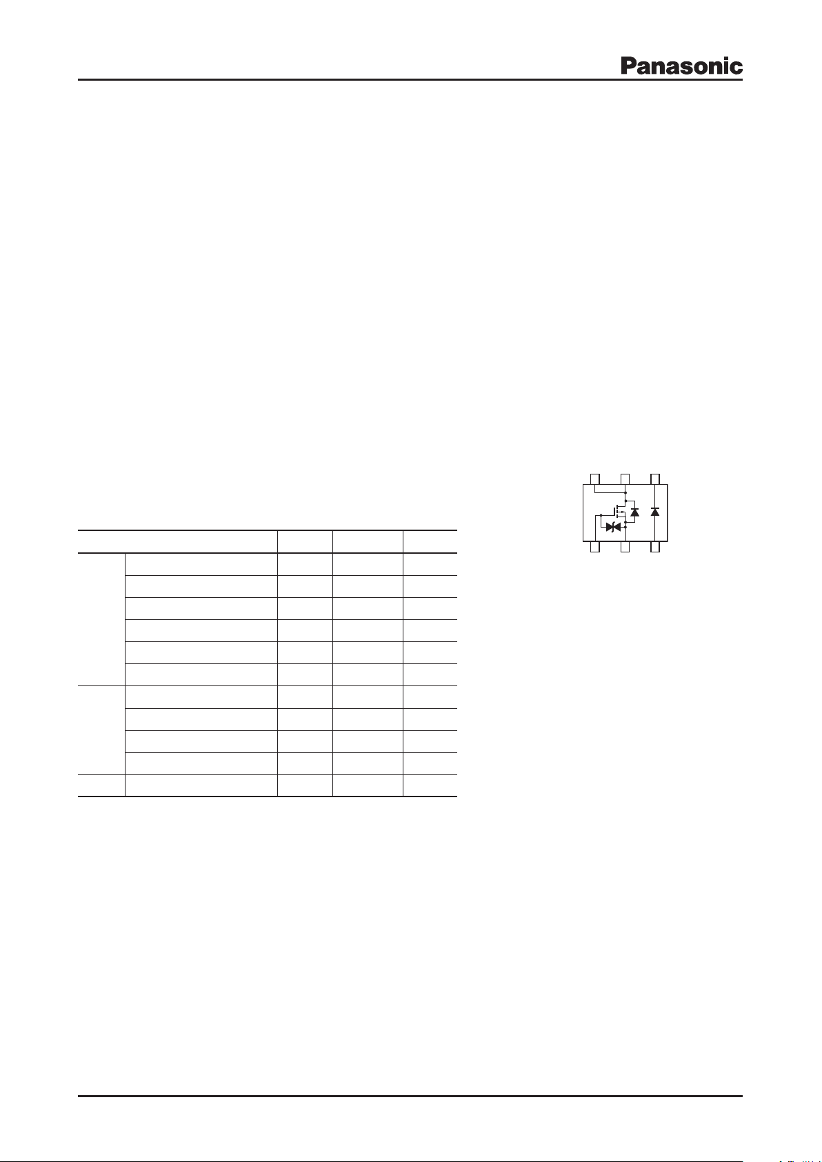
Multi Chip Discrete
MTM86627
Silicon P-channel MOS FET (FET)
Silicon epitaxial planar type (SBD)
For DC-DC converter
For switching circuits
Overview
MTM86627 is the composite MOS FET (P-channel MOS FET and Schttoky
Barrier Diode) that is highly suitable for DC-DC converter and other switching
circuits.
Features
Built-in schottky barrier diode: VR = 15 V, IF = 700 mA
Low on-resistance: Ron = 80 mW (VGS = –4.0 V)
Low
short-circuit input capacitance (Common source)
Small package: WSSMini6-F1 (1.6 mm × 1.6 mm × 0.5 mm)
Low drive Voltage: 1.8 V drive
: C
= 300 pF
iss
Package
Code
WSSMini6-F1
Pin Name
1: Gate 4: Cathode
2: Source 5: Drain
3: Anode 6: Drain
Marking Symbol: PK
Internal Connection
Absolute Maximum Ratings Ta = 25°C
Parameter Symbol Rating Unit
Drain-source surrender voltage V
Gate-source surrender voltage V
Drain current I
FET
Peak drain current I
Channel temperature
Storage temperature T
Reverse voltage V
Forward current (Average) I
SBD
Junction temperature T
Storage temperature T
Overall Total power dissipation
Note) *: Measuring on ceramic substrate at 40 mm × 38 mm × 0.2 mm
Absolute maximum rating without heat sink for PD is 150 mA
*
DSS
GSS
D
DP
T
ch
stg
R
F(AV)
stg
P
D
j
–20 V
±10
–2.0 A
–8.0 A
150
–55 to +150
15 V
700 mA
125
–55 to +125
540 mW
V
°C
°C
°C
°C
Publication date: March 2008 SJF00085AED 1
This product complies with the RoHS Directive (EU 2002/95/EC).
VCC = −10 V
PW = 10 µs
Duty Cycle ≤ 1%
ID = −1.0 A
RL = 10 Ω
V
OUT
V
IN
D
G
S
V
IN
50 Ω
t
d(on)
t
d(off)
0 V
−4 V
V
IN
V
OUT
10%
90%
90%
10%
t
r
t
f
MTM86627
Electrical Characteristics Ta = 25°C±3°C
FET
Parameter Symbol Conditions Min Typ Max Unit
Drain-source surrender voltage V
Drain-source cutoff current
Gate-source cutoff current
Gate threshold voltage V
1
Drain-source ON resistance
Forward transfer admittance
*
1
*
Short-circuit input capacitance (Common source)
Short-circuit output capacitance (Common source)
Reverse transfer capacitance (Common source)
2
Turn-on delay time
Rise time
*
Turn-off delay time
2
Fall time
Note) 1. Measuring methods are based on JAPANESE INDUSTRIAL STANDARD JIS C 7030 measuring methods for transistors.
2. *1: Pulse measurement
*2: ton , t
*
*
2
2
*
measurement circuit
off
DSSID
I
DSS
I
GSS
THID
R
DS(on)
Yfs
C
iss
C
oss
C
rss
t
d(on)
t
r
t
d(off)
t
f
= –1.0 mA, VGS = 0 –20 V
VDS = –20 V, VGS = 0 –1.0
VGS = ±8 V, VDS = 0
= –1.0 mA, VDS = –10 V – 0.4 – 0.75 –1.1 V
ID = –1.0 A, VGS = –4.0 V 80 120
ID = –1.0 A, VGS = –2.5 V 100 170
ID = – 0.5 A, VGS = –1.8 V 140 230
ID = –1.0 A, VDS = –10 V, f = 1 MHz 3.0 S
300 pF
VDS = –10 V, VGS = 0, f = 1 MHz
30 pF
35 pF
VDD = –10 V, VGS = 0 V to –4 V, ID = –1 A
VDD = –10 V, VGS = –4 V to 0 V, ID = –1 A
6 ns
8 ns
57 ns
55 ns
mA
±10 mA
mW
SBD
Parameter Symbol Conditions Min Typ Max Unit
Forward voltage V
Reverse current I
Note) Measuring methods are based on JAPANESE INDUSTRIAL STANDARD JIS C 7031 measuring methods for diodes.
2 SJF00085AED
IF = 500 mA 0.42 V
F
IF = 700 mA 0.45 V
VR = 6 V 90
R
VR = 15 V 250
mA
mA
 Loading...