

Page 1
ORDER NO. MD0004055C3
CD Stereo System
SA-AK18
Colour
(S)... Silver Type
Area
(GC)...Asia, Latin America, Africa and Middle Near East
(GN)...Oceania
TAPE SECTION :
AR2 MECHANISM SERIES
CD SECTION :
RAE0152Z-3 TRAVERSE DECK SERIES
Specifications
■ AMPLIFIER SECTION (GC area)
PMPO 1400 W
RMS power output
THD 10%, both channels driven 70 W per channel (6 Ω)
Input sensitivity
AUX 250 mV
MIC 0.7 mV
Input Impedance
AUX 13.9 kΩ
MIC 680 Ω
■ AMPLIFIER SECTION (GN area)
RMS power output
THD 10%, both channels driven 60 W per channel (6 Ω)
Input sensitivity
AUX 250 mV
Input Impedance
AUX 13.9 kΩ
■ FM TUNER SECTION
Frequency range 87.5 - 108 MHz (50 kHz steps)
Sensitivity 2.5 µV (IHF)
S/N 26 dB 2.2 µV
Antenna terminal(s) 75 Ω (unbalanced)
■ AM TUNER SECTION (GC area)
Frequency range
MW 522 - 1629 kHz (9 kHz steps)
520 - 1630 kHz (10 kHz steps)
SW 3.200 - 7.350 MHz (0.005 MHz
steps)
9.400 - 21.750 MHz (0.005 MHz
steps)
Sensitivity
MW
S/N 20 dB (at 999 kHz) 560 µV/m
SW
S/N 20 dB (at 5.3 MHz) 35.5 µV/m
■ AM TUNER SECTION (GN area)
Frequency range 522 - 1629 kHz (9 kHz steps)
Sensitivity
S/N 20 dB (at 999 kHz) 560 µV/m
■ CASSETTE DECK SECTION
Track system 4 track, 2 channel
Heads
Record/playback Solid permalloy head
Erasure Double gap ferrite head
Motor DC servo motor
© 2000 Matsushita Electronics (S) Pte Ltd. All rights
reserved. Unauthorized copying and distribution is a
violation of law.
Page 2
SA-AK18
Recording system AC bias 100 kHz
Erasing system AC erase 100 kHz
Tape speed 4.8 cm/s
Frequency response (+3 dB, -6 dB at DECK OUT)
NORMAL (TYPE I) 35 Hz - 14 kHz
HIGH (TYPE II) 35 Hz - 14 kHz
S/N 50 dB (A weighted)
Wow and flutter 0.18% (WRMS)
Fast forward and rewind time Approx. 120 seconds with
C-60 cassette tape
■ CD SECTION
Sampling frequency 44.1 kHz
Decoding 16 bit linear
Beam source/wave length Semiconductor laser/780 nm
Number of channels Stereo
Frequency response 20 Hz - 20 kHz (+1, -2 dB)
Wow and flutter Below measurable limit
Digital filter 8fs
D/A converter MASH (1 bit DAC)
■ GENERAL (GC area)
Power supply AC 110 V/127 V/220 V/230-240V,
Power consumption 155 W
50/60 Hz
Power consumption in standby mode
Eco mode on 0.8 W
Eco mode off 12 W
Dimensions (W x H x D) 270 x 330 x 310 mm
Weight 7.4 kg
■ GENERAL (GN area)
Power supply AC 230-240V, 50 Hz
Power consumption 152 W
Power consumption in standby mode
Eco mode on 0.4 W
Eco mode off 12 W
Dimensions (W x H x D) 270 x 330 x 310 mm
Weight 6.9 kg
■ SYSTEM
SC-AK18 (GC) Music Center: SA-AK18 (GC)
Speaker: SB-AK18 (GC)
SC-AK18 (GN) Music Center: SA-AK18 (GN)
Speaker: SB-AK18 (GC)
Notes:
1. Specifiacations are subject to change without notice. Weight and
dimensions are approximate.
2. Total harmonic distortion is measured by the digital spectrum
analyzer.
CONTENTS
Page Page
1 Before Repair and Adjustment
2 Protection Circuitry
3 Accessories
4 Handling Precautions For Traverse Deck
5 Precaution of Laser Diode
6 Operation Procedures
7 Operation Checks and Main Component Replacement
Procedures 8
8 Self-Diagnostic Function
9 Description of Error Code
3
10 CD Test Mode Function
3
11 Measurem ents and Adjustments
12 Illustration of IC’s, Transistors and Diodes
3
4
13 Terminal Function of ICs
14 Block Diagram
4
6
15 Schematic Diagram
16 Printed Circuit Board
17 Wiring Connection Diagram
18 Troubleshooting Guide
15
16
19 Parts Location and Replacement Parts List
17
17
21
22
25
33
60
73
74
75
2
Page 3
1 Before Repair and Adjustment
Disconnect AC power, discharge Power Supply Capacitors C536, C545, C546, C548 and C555 through a 10 Ω, 5W resistor to
ground.
DO NOT SHORT-CIRCUIT DIRECTLY (with a screwdriver blade, for instance), as this may destroy solid state devices.
After repairs are completed, restore power gradually using a variac, to avoid overcurrent.
For GC
Current consumption at AC 110 V, 240 V, 50 Hz in NO SIGNAL mode should be ~620mA ,~300mA respectively.
For GN
Current consumption at AC 240 V, 50 Hz in NO SIGNAL mode should be ~200mA.
2 Protection Circuitry
The protection circuitry may have operated if either of the following conditions are noticed:
• No sound is heard when the power is turned on.
• Sound stops during a performance.
The function of this circuitry is to prevent circuitry damage if, for example, the positive and negative speaker connection wires are
“shorted”, or if speaker systems with an impedance less than the indicated rated impedance of the amplifier are used.
If this occurs, follow the procedure outlines below:
1. Turn off the power.
2. Determine the cause of the problem and correct it.
3. Turn on the power once again after one minute.
Note:
When the protection circuitry functions, the unit will not operate unless the power is first turned off and then on again.
SA-AK18
3 Accessories
Remote Control Transmitter
FM indoor antenna
AC mains lead (GC)
Power plug adapter (GC)
AM Loop antenna
AC mains lead (GN)
3
Page 4
SA-AK18
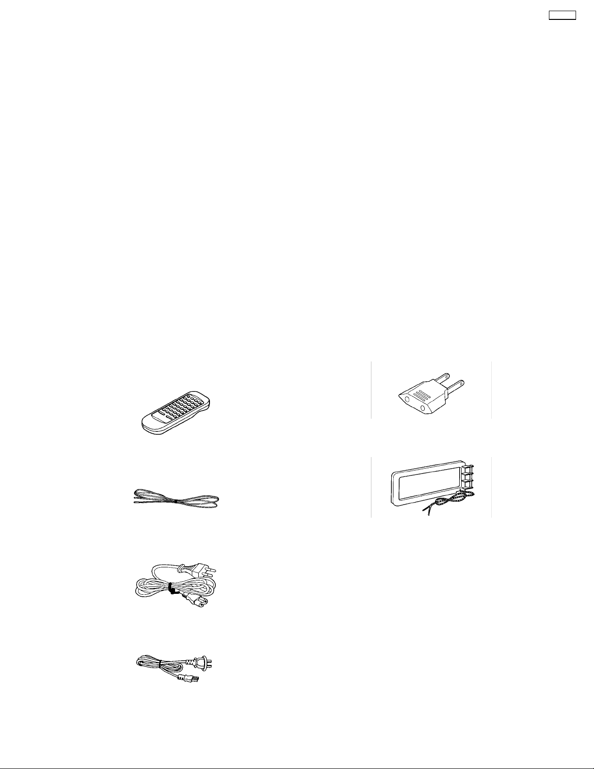
4 Handling Precautions For Traverse Deck
The laser diode in the traverse deck (optical pickup) may break
down due to potential difference caused by static electricity of
clothes or human body.
So, be careful of electrostatic breakdown during repair of the
traverse deck (optical pickup).
● Handling of traverse deck (optical pickup)
1. Do not subject the traverse deck (optical pickup) to
static electricity as it is extremely sensitive to electrical
shock.
2. The short land between the No.4 (LD) and No.5 (GND)
pins on the flexible board (FFC) is shorted with a solder
build-up to prevent damage to the laser diode.
To connect to the PC board, be sure to open by
removing the solder build-up, and finish the work
quickly.
3. Take care not to apply excessive stress to the flexible
board (FFC board).
4. Do not turn the variable resistor (laser power
adjustment). It has already been adjusted.
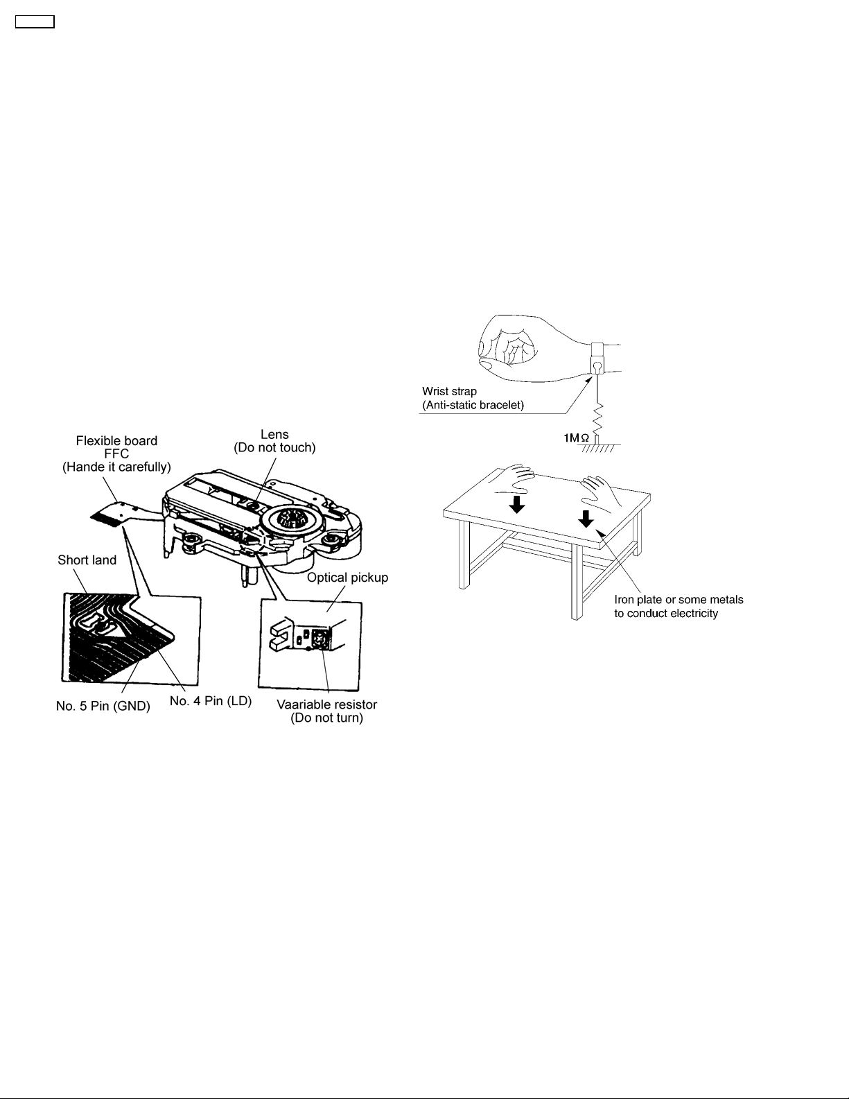
● Grounding for electrostatic breakdown prevention
1. Human body grounding
Use the anti-static wrist strap to discharge the static
electricity from your body.
2. Work table grounding
Put a conductive material (sheet) or steel sheet on the
area where the traverse deck (optical pickup) is placed,
and ground the sheet.
Caution :
The static electricity of your clothes will not be grounded
through the wrist strap. So, take care not to let your
clothes touch the traverse deck (optical pickup).
Caution when Replacing the Traverse Deck :
The traverse deck has a short point shorted with solder to
protect the laser diodeagainst electrostatics breakdown.Be
sure to remove the solder from the short point before
making connections.
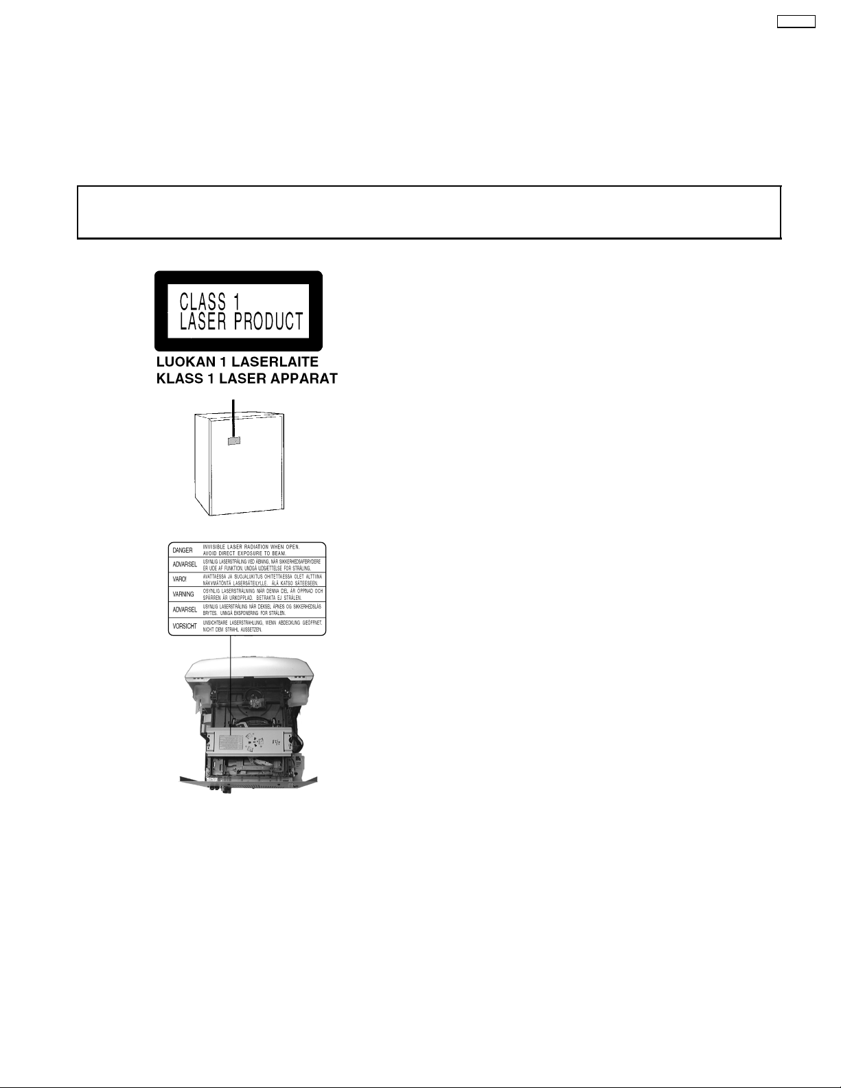
5 Precaution of Laser Diode
Caution :
This product utilizes a laser diode with the unit turned "ON", invisible laser radiation is emitted from the pick up lens.
Wavelength : 780 nm
Maximum output radiation power from pick up : 100 µW/VDE
Laser radiation from pick up unit is safety level, but be sure the followings:
1. Do not disassemble the optical pick up unit, since radiation from exposed laser diode is dangerous.
2. Do not adjust the variable resistor on the pick up unit. It was already adjusted.
3. Do not look at the focus lens using optical instruments.
4. Recommend not to look at pick up lens for a long time.
ACHTUNG :
Dieses Produkt enthält eine Laserdiode. Im eingeschalteten Zustand wird unsichtbare Laserstrahlung von der Lasereinheit
abgestrahlt.
Wellenlänge : 780nm
4
Page 5
Maximale Strahlungsleistung der Lasereinheit :100W/VDE
Die Strahlung an der Lasereinheit ist ungefährlich, wenn folgende Punkte beachtet werden:
1. Die Lasereinheit nicht zerlegen, da die Strahlung an der freigelegten Laserdiode gefährlich ist.
2. Den werkseitig justierten Einstellregler der Lasereinhit nicht verstellen.
3. Nicht mit optischen Instrumenten in die Fokussierlinse blicken.
4. Nicht über längere Zeit in die Fokussierlinse blicken.
ADVARSEL: I dette a apparat anvendes laser.
CAUTION!
THIS PRODUCT UTILIZES A LASER.
USE OF CONTROLS OR ADJUSTMENTS OR PERFORMANCE OF PROCEDURES OTHER THAN THOSE SPECIFIED HEREIN MAY RESULT
IN HAZARDOUS RADIATION EXPOSURE.
■ Use of Caution Labels
SA-AK18
5
Page 6
SA-AK18
6 Operation Procedures
6
Page 7
SA-AK18
7
Page 8
SA-AK18
7 Operation Checks and Main Component Replacement
Procedures
“ATTENTION SERVICER”
Some chassis components may have sharp edges.
Be careful when disassembling and servicing.
1. This section describes procedures for checking the operation of the major printed circuit boards and replacing the
main components.
2. For reassembly after operation checks or replacement, reverse the respective procedures.
Special reassembly procedures are described only when required.
3. Select items from the following index when checks or replacement are required.
Contents
• Checking Procedure for each major P.C.B.
1. Checking of the Main, Panel, Deck and Power P.C.B.
• Main Component Replacement Procedures
1. Replacement of the Traverse Deck.
2. Replacement of the Power Amplifier IC.
• Disassembly and assembly of the Traverse Unit
• Disassembly and assembly of the Disc Tray
Warning:
This product uses a laser diode. Refer to caution statement “Precaution of Laser Diode.
ACHTUNG:
• Die Lasereinheit nicht zerlegen.
• Die Lasereinheit darf nur gegen eine vom Hersteller speczifizierte Einheit ausgetauscht werden.
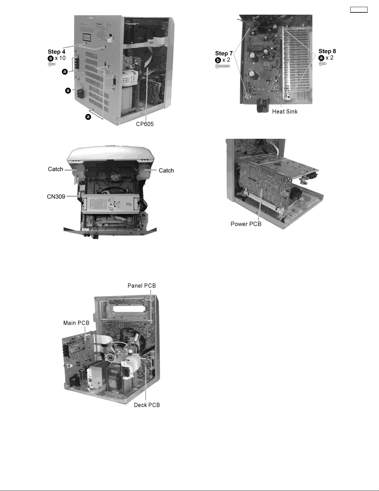
7.1. Checking Procedure for each major P.C.B.
7.1.1. Checking of the Main, Panel, Deck
and Power P.C.B.
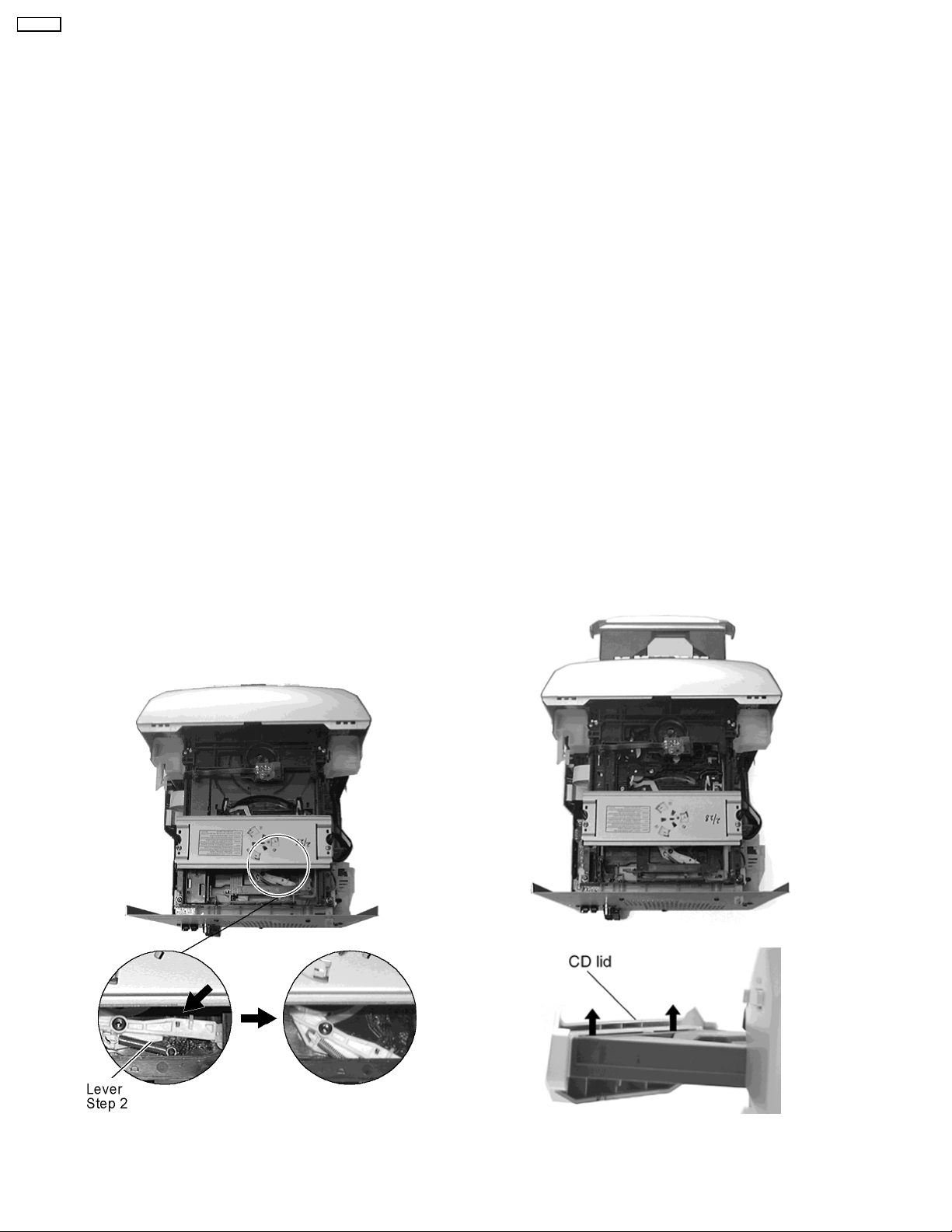
Step 1 Remove the Top Cabinet.
Step 2 Push the lever in the direction of the arrow.
Step 3 Pull out the CD tray as shown and remove the CD lid.
Push back the CD tray after the CD lid has been removed.
8
Page 9
SA-AK18
Step 5 Remove the wire at CP605 and CN309.
Step 6 Release the 2 catches and remove the CD changer
base together with the CD changer.
• Checking for Main, Panel and Deck P.C.B
• Checking for Power P.C.B.
9
Page 10
SA-AK18
7.2. Main Component Replacement Procedures
7.2.1. Replacement of the Traverse Deck
Step 1
Unit’ (
Follow the procedures in ‘Disassembly of the Traverse
Step 1 - Step 4
).
Note:
Insert a short pin into the flexible cable for traverse unit.
Installation of the CD servo P.C.B. after replacement
•
Step 1
Step 2
assembly.
Connect the FFC board.
Install the CD servo P.C.B. in the traverse deck
Step 3
Servo P.C.B.
Step 4
the 3 pins. Then remove the Traverse Deck.
Desolder the 4 legs of the 2 motors and pull out the
Widen the 3 bosses with a flat screwdriver and pull out
Note:
Before installing the CD servo P.C.B., move the optical pickup
towards the outer edge from the marking (black triangle).
[Otherwise, the reset detect switch (S701) mounted on the CD
servo P.C.B. may be damaged.]
Step 5
• Removal of the flexible cable. Push the top of the connector
Remove the flexible cable CN701.
in the direction of the arrow 1, and then pull out the flexible
cable in the direction of the arrow 2.
10
Page 11
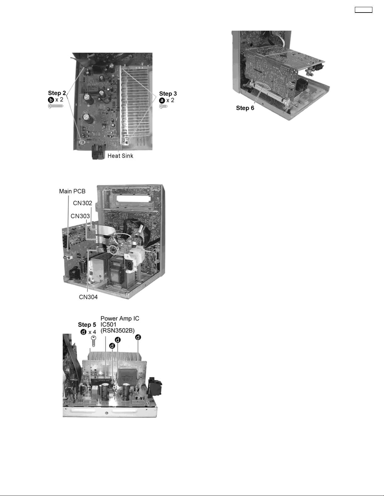
7.2.2. Replacement of the Power
Amplifier IC
Step 1
Follow the procedures in ‘Checking Procedure for each
major P.C.B.’ (
Step 1 - Step 6
).
Step 6
the respective component.
Unsolder the terminals of Power Amp IC and replace
SA-AK18
Step 4
pull out the Main PCB.
Step 5
Remove the wires at CN302, CN303 and CN304 and
Remove the 4 screws fixed to the Power Amplifier IC.
11
Page 12
SA-AK18
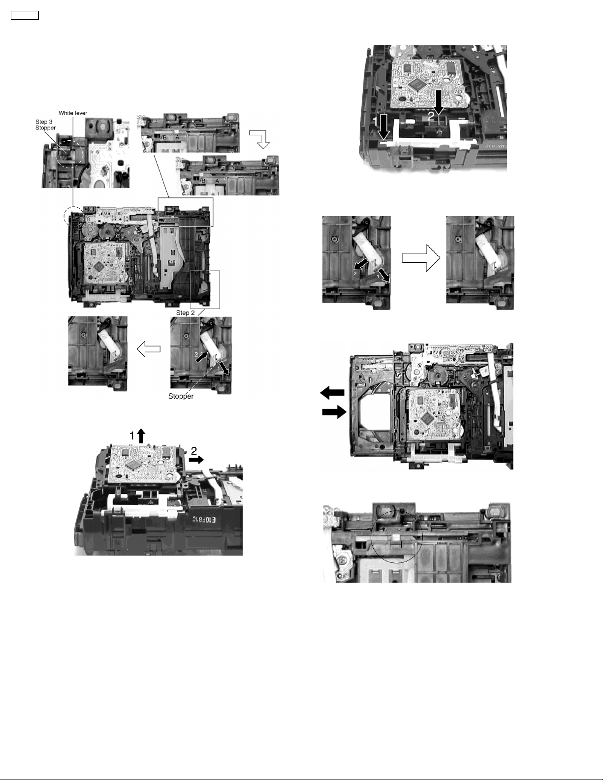
7.3. Disassembly and assembly of the Traverse Unit
Step 1 Push the lever from position A to B.
Step 2 Pull the stopper (black) in the direction of arrow 1 and
push the lever in the direction of arrow 2.
Step 3 Push the stopper (black) down until the white lever eject
out.
Step 3 Pull the stopper in the direction of arrow 1 and release
the lever in the direction of arrow 2 as shown.
Step 4 Lift up the traverse unit and slide out the unit as shown.
• Replacement of Traverse Unit
Step 1 Place the traverse unit as shown.
Step 2 Press in the lever shaft in the direction of arrow 1 as
shown and push the traverse unit into the position in the
direction of arrow 2.
Step 4 Pull out the tray half way and push it back fully.
Step 5 Push the lever to the initial position indicated ‘|---|’.
12
Page 13
7.4. Disassembly and assembly of the Disc Tray
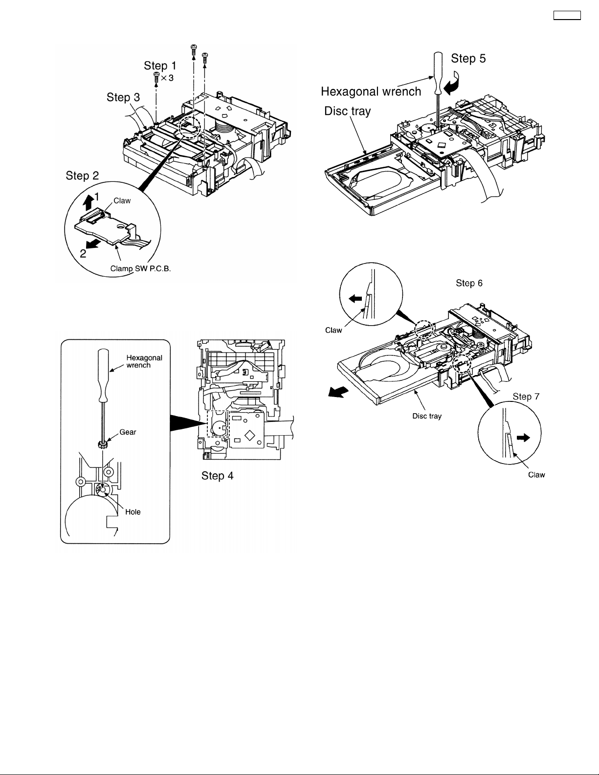
Step 5 Rotate the hexagonal wrench in the direction of arrow
(clockwise), and then open the disc tray fully.
Step 2 With lifting the claw in the direction of arrow 1, draw the
clamp SW P.C.B. in the direction of arrow 2.
Step 3 Remove the mechanism cover.
SA-AK18
Step 4 Insert the gear with hexagonal wrench into the hole.
Step 6 Upset the CD changer unit again.
Step 7 Release both the claws, and then draw the disc tray.
13
Page 14
SA-AK18
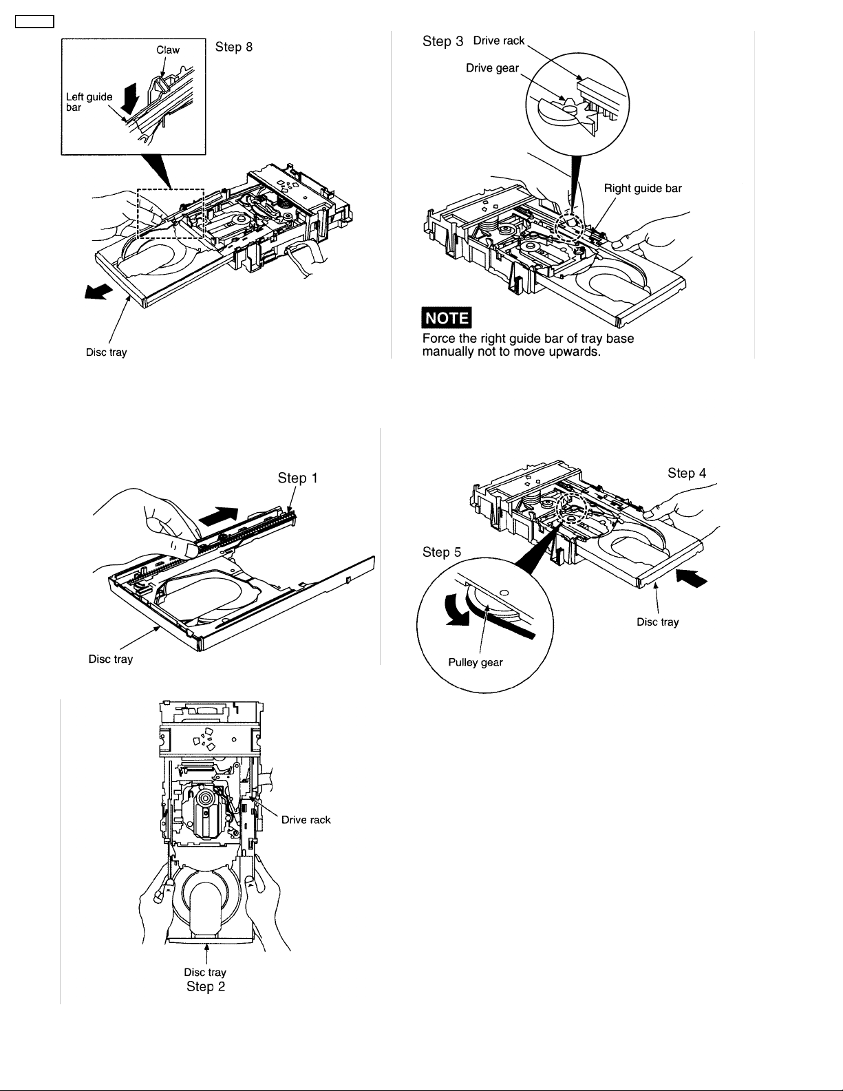
Step 8 With forcing the left guide bar manually because the left
guide bar interferes with claw, draw the disc tray.
• Installation of the disc tray after replacement
Step 1 Slide the drive rack fully in the direction of the arrow.
Step 3 Align the drive rack with the drive gear.
Step 4 Holding the disc tray manually, rotate the pulley gear in
the direction of arrow.
Step 5 Rotate the gear 5 or 6 times manually, and then push
the disc tray.
Step 2 Holding the drive rack, not to move, install the disc tray.
14
Page 15
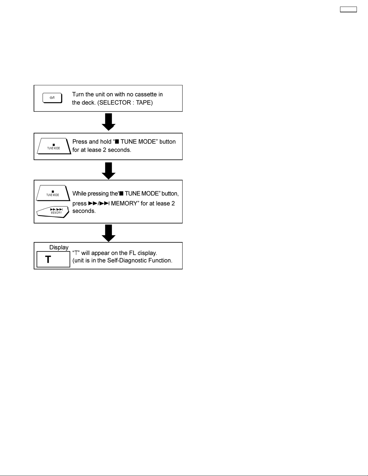
8 Self-Diagnostic Function
8.1. Self-diagnostic display
This unit is equipped with a self-diagnostic display function which, if a problem occurs, will display an error code corresponding to
the problem.
Use this function when performing maintenance on the unit.
8.2. How to enter the Self-Diagnostic Function
SA-AK18
8.3. Cassette Mechanism Test (For error code H01, H02, H03, F01, F02)
1. Press “TAPE, DECK 1/2” to select Deck 2.
2. Load a cassette tape with the erasure prevention tab, remove from left side only and close the cassette holder.
3. Press “FAST FORWARD MEMORY” (Tape will be stop after 2 seconds)
4. Load a cassette tape with the erasure prevention tab, remove from right side only and close the cassette holder.
5. Press “REVERSE FM MODE/BP” (Tape will be stop after 2 seconds)
6. Load a pre-recorded tape with both side record tabs intact and close the cassette holder.
7. Press “PLAY/TUNE/TIME ADJ UP” (After TPS function, tape will stop automatically)
8. Press “REC/STOP” (Tape will not move)
9. Press “STOP/TUNE MODE” to indicate Error code.
• If several problem exist, error code will change each time when “■ /TUNE MODE” is pressed.
(e.g. H01 → H03 → F01 .....etc.)
10. Press “TAPE, DECK 1/2” to select Deck 1.
11. Repeat step 2 to 9 to test Deck 1. (Tape Deck 1 will not check H02 because of no recording function)
8.4. CD Mechanism Test (F15, F26, F16, F17, F27, F28, F29, H15, F75)
1. Press “CD”.
2. Press “OPEN/CLOSE (1)” and place a CD.
3. Press “OPEN/CLOSE (1)” to close the tray.
15
Page 16
SA-AK18
4. Press “OPEN/CLOSE (5)” and wait until the tray is open.
5. Press “OPEN/CLOSE (1)” and remove the CD.
6. Press “OPEN/CLOSE (1)” to close the tray.
7. Press “■/TUNE MODE” to indicate Error Code.
• If several problem exist, error code will change each time when “■/TUNE MODE” is pressed. (e.g. F15 → F26 → F16 ....etc).
8.5. To clear all Error code
1. Press “STOP/TUNE MODE” button for 5 seconds.
2. FL indicator shows “CLEAR” for 1 second and change to “T”.
8.6. How to get out from Self-Diagnostic function
1. Press “Power” button OFF.
8.7. Power Amplifier Failure (F61)
1. When power amplifier fail, F61 will indicate automatically.
9 Description of Error Code
9.1. Error detection for Cassette Mechanism block
No. Error Error
1 MODE SW
detection error
2 REC INH SW
detection error
3 HALF SW
detection error
4 Reel Pulse
detection error
5 TPS abnormal F02 Cassette deck will not perform TPS function.
Display
H01 Faulty operation of cassette mechanism.
H02 Recording not possible.
H03 Playback cannot perform.
F01 The tape advances slightly and then stops.
Problem condition
Faulty contact or short-circuit of mechanism mode switch (S951, S971).
Faulty contact or short-circuit of REC INH switch (S974, S975).
Faulty contact or short-circuit of HALF siwtch (S952, S972).
Faulty reel pulse, faulty hole detect IC (IC951, IC971).
Faulty playback EQ/recording amplifier IC (IC101).
9.2. Error detection for CD/Changer block
No. Error Error
1 REST SW detection error F15 CD does not function.
2 CD tray opens automatically F16 CLAMP switch (S4) NG (Check & Replace)
3 Does not startup when [PLAY]
button is pressed
4 Transmission error between CD
servo LSI and micon
5 Startup fails even when you
insert CD or the selected disc tray
does not open
6 Cannot insert CD F28 Tray 1 detect switch NG (Check & Replace)
7 Cannot eject CD F29 Check if disc is stuck. Tray 2 detect switch NG (Confirm & Replace)
8 The CD tray closes H15 CD disc tray detect switch NG (S3) (Check & Replace)
Display
F17 BOTTOM switch (S5) NG (Check & Replace)
F26 CD does not function.
F27 Tray 1 detect switch or Tray 2 detect switch NG (Check & Replace)
Problem condition
This error occurs when the Optical Pick Up REST SW (S701) is not
detected within the specified time (about 8 seconds)
This error occurs when the POWER is ON for the CD block and an error
is detected after the transmission has started.
9.3. Power Supply related error detection
No. Error Error
1 POWER AMP
output abnormal
Display
F61 When POWER is switched on, power become off automatically.
Problem condition
During normal operation, if DC DET become L, PCNT shall become
L and the error display on the left shall be displayed. (IC501)
16
Page 17
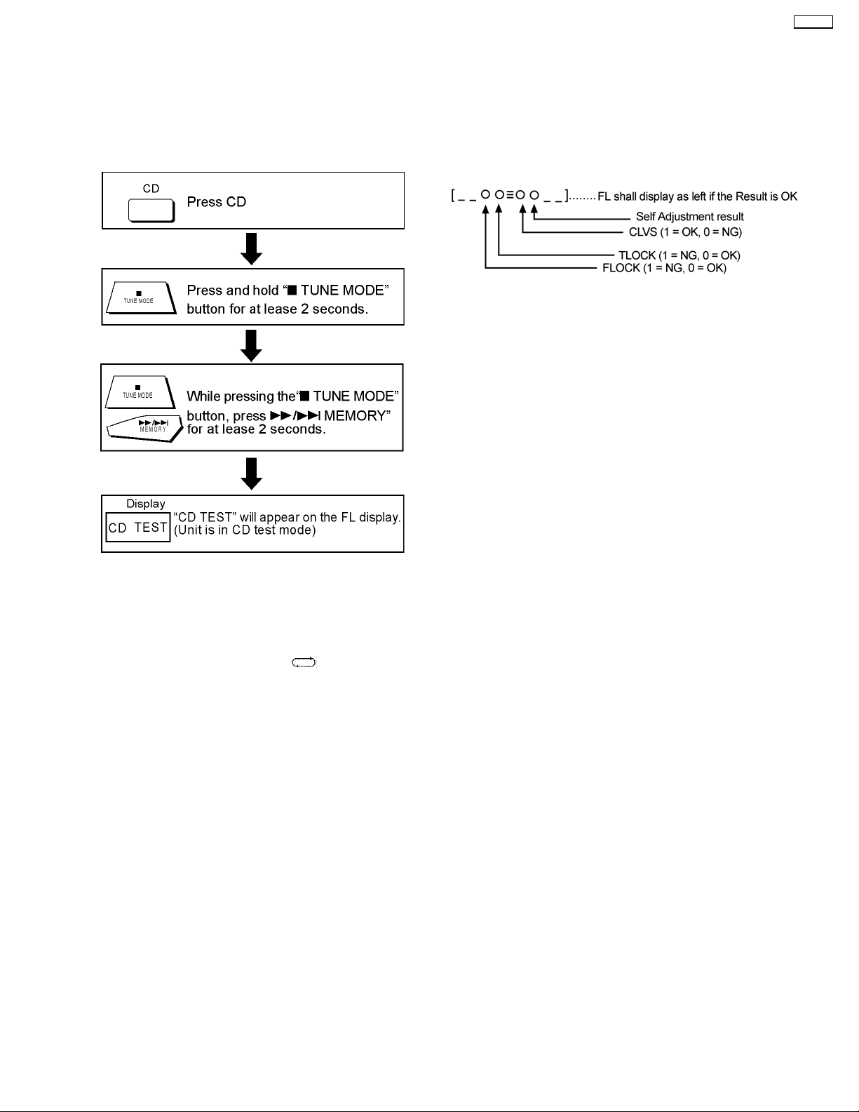
10 CD Test Mode Function
SA-AK18
This CD test mode is provided to check CD unit without
connecting to changer loading mechanism. This mode shall
operate CD PLAY with CD unit being connected only and CD
Automatic Alignment result is shown on FL display.
10.1. How to set CD test mode
10.2. CD Automatically Adjustment
result indication
Under CD test mode, pressing the numeric key ‘0’ on the
remote controller will display the auto adjustment result.
FLOCK, TLOCK and CLVS status shall be shown as below:
During the above display, executing CD PLAY will display auto
adjustment result for CD PLAY mode.
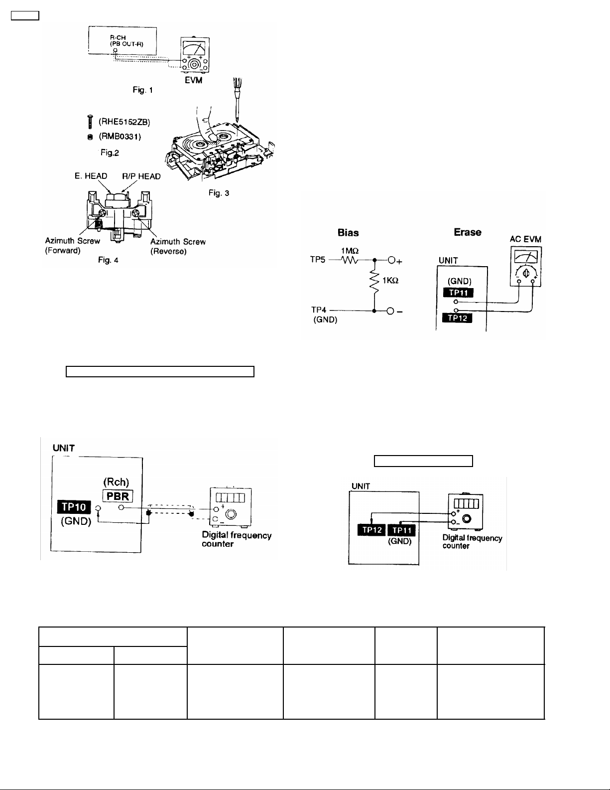
11 Measurements and Adjustments
11.1. Cassette Deck Section
• Measurement Condition
− Reverse-mode selector switch:
− Tape edit: NORMAL
− Record timer: OFF
− Make sure head, capstan and press roller are clean.
− Judgeable room temperature 20 ± 5 °C (68 ± 9°F)
• Measuring instrument
− EVM (Electronic Volmeter)
− Digital quency counter
• Test Tape
− Head azimuth adjustment (8 kHz, -20 dB); QZZCFM
− Tape speed gain adjustment (3 kHz, -10 dB);
QZZCWAT
− Playback gain adjustment (315 Hz, 0 dB); QZZCFM
− CrO2 tape, QZZCRX
11.1.1. Head Azimuth Adjustment (Deck
1/2)
wish to readjust the head azimuth without replacing the
acrews and springs, a fine adjustment to the azimuth screw
and spring.
• Please remove the screw-locking bond left on the head
base when replacing the azimuth screw.
• If you wish to readjust the head azimuth, be sure to adjust
with adhering the cassette tape closely to the mechanism
by pushing the center of cassette tape with your finger.
(shown in Fig. 3)
1. Playback the azimuth adjustment portion (8 kHz, -20dB) of
the test tape (QZZCFM) in the forward play mode. Vary the
azimuth adjustment screw until the output of the R-CH (PB
OUT-R) are maximized.
2. Perform the same adjustment in the reverse play mode.
3. After the adjustment, apply screwlock to the azimuth
adjusting screw.
Caution:
• Please replace both azimuth adjustment screw
(RHE5152ZB) and springs (RM0331) simultaneously when
readjusting the head azimuth. (shown in Fig. 2) Even if you
17
Page 18
SA-AK18
11.1.2. Tape Speed Adjustment (Deck 1/2)
11.1.3. Bias and Erase Voltage Check
1. Set the unit “AUX” position.
2. Insert the Normal blank tape (QZZCRA) into DECK 2 and
the unit to “REC” mode (use “● REC/STOP” key).
3. Measure and make sure that the output is within the
standard value.
4. Insert the CrO2 tape (QZZCRX).
5. Repeat step 2 and 3.
Bias voltage for Deck 2 14 ± 4mV (Normal)
Standard value) 17 ± 5mV (CrO2)
Erase voltage for Deck 2 more than 80mV (Normal)
more than 90mV (CrO2)
1. Set the tape edit button to “NORMAL” position.
2. Insert the test tape (QZZCWAT) to DECK 2 and playback
(FWD side) the middle portion of it.
3. Adjust Motor VR (DECK 2) for the output value shown
below.
Adjustment target: 2940 ~3060Hz(NORMAL speed)
4. After alignment, assure that the output frequency of the
DECK 2 REV and DECK 1 FWD are within ±45Hz and ±60
Hz respectively of the value of the output frequency of
DECK 2 FWD.
11.1.4. Bias Frequency Adjustment (Deck
1/2)
1. Set the unit to “AUX” position.
2. Insert the Normal blank tape (QZZCRA) into DECK 2 and
set the unit to “REC” mode (● use “REC/STOP” key).
3. Adjust L1002 so that the output frequency is within the
standard value.
Standard Value: 97 ±8 kHz
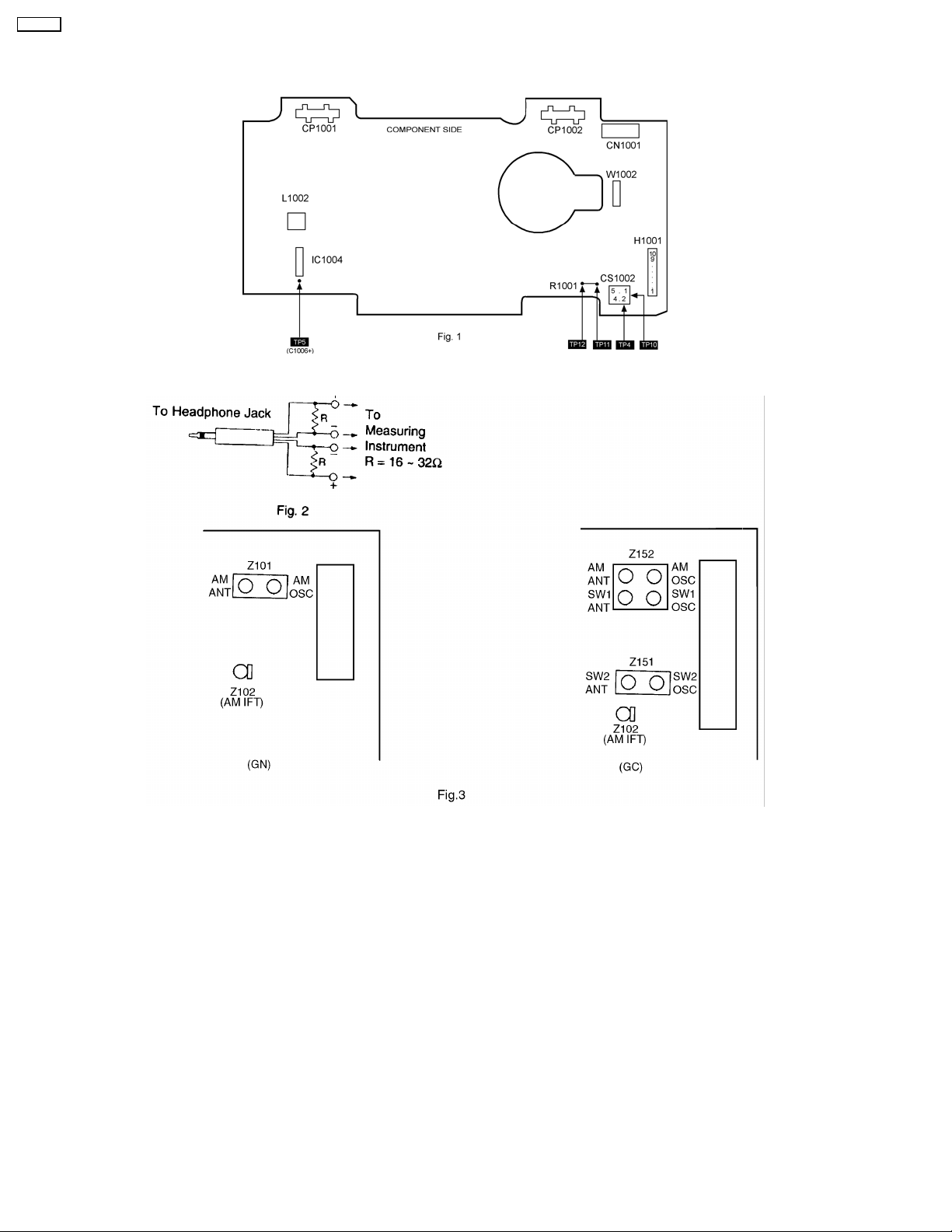
11.2. Tuner Section
11.2.1. AM-IF Alignment
SIGNAL GENERATOR OR SWEEP
CONNECTIONS FREQUENCY
Fashion a loop of
several turns of wire
and radiate a signal
into the loop ant. of
receiver.
GENERATOR
450 kHz 30% Mod.
at 400Hz.
RADIO DIAL SETTING INDICATOR
Point of non-interference
(on/about 600 kHz)
(ELECTRONIC
VOLTMETER
OSCILLOSCOPE)
Headphones Jack (32Ω)
Fabricate the plug as
shown in Fig. 2 and then
connect the lead wires of
the plug to the
measuring instrument.
18
ADJUSTMENT
(Shown in
Fig.3)
Z102 (AM IFT) Adjust for maximum output.
REMARKS
Page 19
11.2.2. AM-RF Alignment
SA-AK18
SIGNAL GENERATOR OR SWEEP
CONNECTIONS FREQUENCY
Fashion a loop of
several turns of wire
and radiate a signal
into the loop ant. of
receiver.
Fashion a loop of
several turns of wire
and radiate a signal
into the loop ant. of
receiver.
GENERATOR
522 kHz Tuning capacitor fully closed Headphones Jack (32Ω)
603 kHz Tuning to signal Headphones Jack (32Ω)
RADIO DIAL SETTING INDICATOR
11.2.3. SW1-RF Alignment (GC)
SIGNAL GENERATOR OR SWEEP
CONNECTIONS FREQUENCY
Fashion a loop of
several turns of wire
and radiate a signal
into the loop ant. of
receiver.
Fashion a loop of
several turns of wire
and radiate a signal
into the loop ant. of
receiver.
GENERATOR
3.2 MHz Tuning capacitor fully closed Headphones Jack (32Ω)
3.2 MHz Tuning to signal Headphones Jack (32Ω)
RADIO DIAL SETTING INDICATOR
(ELECTRONIC
VOLTMETER
OSCILLOSCOPE)
Fabricate the plug as
shown in Fig. 2 and then
connect the lead wires of
the plug to the
measuring instrument.
Fabricate the plug as
shown in Fig. 2 and then
connect the lead wires of
the plug to the
measuring instrument.
(ELECTRONIC
VOLTMETER
OSCILLOSCOPE)
Fabricate the plug as
shown in Fig. 2 and then
connect the lead wires of
the plug to the
measuring instrument.
Fabricate the plug as
shown in Fig. 2 and then
connect the lead wires of
the plug to the
measuring instrument.
ADJUSTMENT
(Shown in
Fig.3)
Z152 (GC),
Z101(GN)
(AM OSC Coil)
Z152 (GC),
Z101(GN)
(AM ANT Coil)
ADJUSTMENT
(Shown in
Fig.3)
Z152
(SW1 OSC
Coil)
Z152
(SW1 ANT Coil)
REMARKS
Adjust for maximum output.
Adjust for maximum output.
REMARKS
Adjust for maximum output.
Adjust for maximum output.
11.2.4. SW2-RF Alignment (GC)
SIGNAL GENERATOR OR SWEEP
CONNECTIONS FREQUENCY
Fashion a loop of
several turns of wire
and radiate a signal
into the loop ant. of
receiver.
Fashion a loop of
several turns of wire
and radiate a signal
into the loop ant. of
receiver.
GENERATOR
9.4 MHz Tuning capacitor fully
9.4 MHz Tuning to signal Headphones Jack (32Ω)
RADIO DIAL SETTING INDICATOR
closed
(ELECTRONIC
VOLTMETER
OSCILLOSCOPE)
Headphones Jack (32Ω)
Fabricate the plug as
shown in Fig. 2 and then
connect the lead wires of
the plug to the
measuring instrument.
Fabricate the plug as
shown in Fig. 2 and then
connect the lead wires of
the plug to the
measuring instrument.
ADJUSTMENT
(Shown in
Fig.3)
Z151
(SW2 OSC Coil)
Z151
(SW2 ANT Coil)
REMARKS
Adjust for maximum output.
Adjust for maximum output.
19
Page 20
SA-AK18
11.3. Alignment Points
Cassette Deck section
Tuner section
20
Page 21
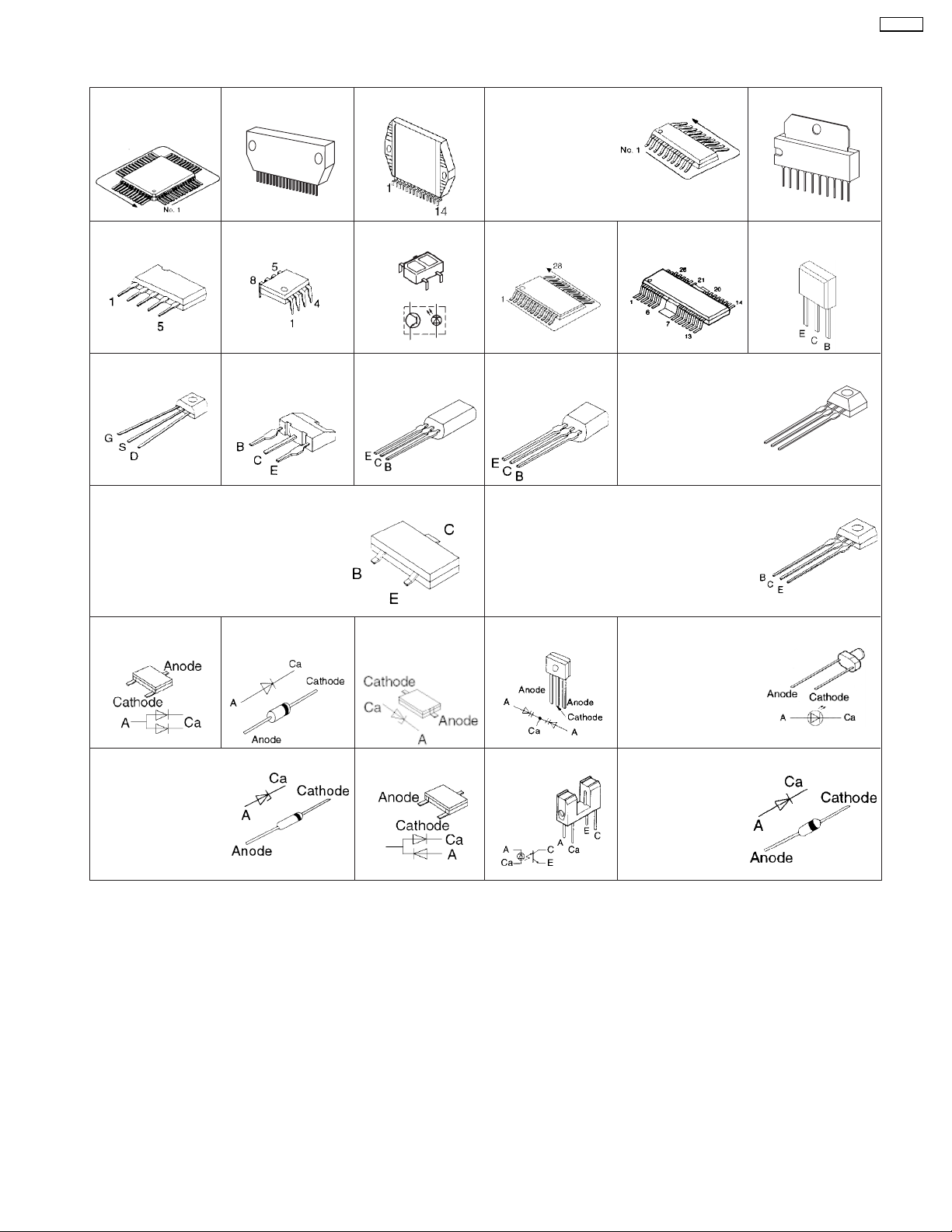
12 Illustration of IC’s, Transistors and Diodes
SA-AK18
M38199MF227 (100P)
M62433AFP (80P)
MN662790RSC (80P)
BA7755A
2SK544F-AC
2SA1037AKSTX
2SC2412KT96R
DTC144TKA146
DTA114EKA146
KRA102STA
DTC114EKA146
STK470-010A
1
19
M5218AP
2SB1238QRTV2
KTC3875GRTA
KRC111STA
KTD1304TA
KRC102STA
DTC143XKA146
RSN3502B
0N2180RLC1
2
1
3
4
2
3
4
1
2SC3940AQSTA
BU2090AF-E2 (16P)
LA1833NMNTLM (24P)
LC72131MDTRM (20P)
AN7348STA-E1 (24P)
BA4558FE2 (8P)
M62457AFPE1 (16P)
AN8839NSBE2 (28P)
KTA12710YTA
2SD965RTA
2SB621ARSTA
2SA933SSTA
2SC1740SSTA
2SC2787FL1TA
2SD2144STA
KTC3199GRTA
RVTDTC143EST
AN8739SBE2
KRC110MTA
KRA102MTA
KRC103MTA
KRC102MTA
2SC2786MTA
2SC2784FTA
RVTDTA114EST
2SC2785FTA
2SA1309ARTA
TA7291P
1
2SA1309ARTA
2SC2058SPTA
B
C
E
10
DAP202KT146
MTZJ10BTA
MTZJ4R7BTA
MTZJ8R2BTA
MTZJ12BTA
MTZJ7R5ATA
MA4020LTA
MTZJ6R8BTA
MTZJ33BTA
MTZJ16BTA
1D3E
RL1N4003S-P
1SS355TE17
UDZSTE175R1B
UDZTE173R6B
DA204KT146
SVC211SPA-AL
SLI325URCT31
SLI325DCT31
SLR325MCT31W
SLR505DCT31
GP1S94
RVD1SS133TA
1SS291TA
MA165TA
MA700ATA
MA723TA
21
Page 22
SA-AK18
13 Terminal Function of ICs
13.1. IC701 (AN8839NSBE2) Servo Amplifier
Pin No. Mark I/O Function
1 PDE I Tracking signal input 1
2 PDF I Tracking signal input 2
3 VCC I Power supply
4 PDA I Focus signal input terminal 1
5 PDB I Focus signal input terminal 2
6 LPD I APC amp input
7 LD O APC amp output
8 RF O RF summing output
9 RFIN I Detector’s input
10 CSBRT I Capacitor for OFTR connection
11 CEA I Capacitor for HPF amp connection
12 BDO O BDO output (“H” : drop out)
13 LDON I APC control
14 GND — Ground
Pin No. Mark I/O Function
15 /RFDET O NRFDET output (“L” : detec tion)
16 PDOWN O Power-down input
17 OFTR O OFTR output
18 NC O N.C.
19 ENV O 3T-ENV output
20 NC I N.C.
21 NC I N.C.
22 TEN I TE amp input
23 TEOUT O TE amp output
24 FEOUT O FE amp output
25 FEN I FE amp input
26 VREF O Reference voltage output
27 TBAL I Tracking balance control
28 FBAL I Focus balance control
13.2. IC702 (MN662790RSC) Servo processor/ Digital signal processor/
Digital filter/ D/A converter
No. Mark I/O Function
1 BCLK O N.C.
2 LRCK O N.C.
3 SRDATA O N.C.
4 DVDD1 I Power supply input (for digital
circuit)
5 DVSS1 I GND (for digital circuit)
6 TX O Digital audio interface signal
output (Latches data at first
transition)
7 MCLK I Microprocessor command
clock signal input
8 MDATA I Microprocessor command
data signal input
9 MLD I Microprocessor command
load signal input
10 SENSE O Sense signal output (OFT,
FESL,MAGEND,NAJEND,PO
SAD,SFG) (Not used, open)
11 /FLOCK O Focus servo feeding signal
output (“L” : Feed)
12 /TLOCK O Tracking servo feeding signal
output (“L” : Feed)
13 BLKCK O Sub-code block clock signal
output (fBLKCK = 75Hz
during normal playback)
14 SQCK I External clock signal input for
sub-code Q resistor
15 SUBQ O Sub-code Q code output
16 DMUTE I Muting input (“H”: mute)
17 STAT O Status signal output
(CRC,CUE,CLVS,TTSTVP,F
CLV,SQCK)
18 /RST I Reset signal input
19 SMCK O 1/2-divided clock signal of
crystal oscillating at MSEL =
“H” (fSMCK = 8.4672 MHz)
1/4-divided clock signal of
crystal oscillating at MSEL =
“L” (fSMCK = 4.2336 MHz)
20 CSEL I Frequency Selection Terminal
H = 33.8688 MHz; L =
16.9344 MHz
21 TRV O N.C.
22 TVD O Traverse drive output
23 PC O Spindle motor ON outpu t ("L"
: ON)
No. Mark I/O Function
24 ECM O Spindle motor drive signal
output(forced mode output)
25 ECS O Spindle motor drive signal
output
(servo error signal output)
26 KICK O N.C.
27 TRD O Tracking drive output
28 FOD O Focus drive output
29 VREF I D/A (drive) output (TVD, ECS,
TRD, FOD, FBAL, TBAL)
Reference voltage input
30 FBAL O Focus balance adjustment
output
31 TBAL O Tracking balance adjustment
output
32 FE I Focus error signal input
(analog input)
33 TE I Tracking error signal input
(analog input)
34 RFENV I RF envelope signal input
35 VDET I Vibration detection signal
input ("H" : detection)
36 OFT I Off-track signal input ("H" : off
track)
37 TRCRS I Track cross signal input
38 /RFDET I RF detection signal input ("L"
: detection)
39 BDO I Dropout signal input ("H" :
Dropout)
40 LDON O Laser on signal output ("H" :
ON)
41 PLLF2 I/O N.C.
42 DSLF2 O Tracking Offset alignment
output/DSL Balance Output
(DA Output)
43 WVEL O N.C.
44 ARF I RF signal input
45 IREF I Reference current input
46 DRF I DSL bias terminal (Not used,
open)
47 DSLF I/O DSL loop filter terminal
48 PLLF I/O PLL loop filter terminal
49 VCOF I/O VCO loop filter terminal
50 AVDD2 I Power supply input (for
analog circuit)
51 AVSS2 I GND (for analog circuit)
22
Page 23
No. Mark I/O Function
52 EFM - EFM signal output
53 PCK - PLL extraction clock output
(fPCK = 4.321 MHz during
normal playback)
54 VCOF2 I/O VCO Loop filter for 33.8688
MHz conversation terminal for
16.9344 MHz crystal mode,
must use other circuit
55 SUBC O Sub-code serial data output
56 SBCK I Clock input for sub-code
serial data
57 VSS I GND
58 X1 IN I Crystal oscillating circuit input
(f = 16.9344MHz)
59 X2 OUT O Crystal oscillating circuit input
(f = 16.9344 MHz)
60 VDD I Power supply input (for
oscillating circuit)
61 BYTCK - Byte clock output
62 /CLDCK - Sub-code frame clock signal
output (fCLDCK = 7.35 kHz
during normal playback)
63 FCLK - Crystal frame clock signal
output (fCLK = 7.35 kHz,
double = 14.7 kHz)
64 IPFLAG - Interpolation flag output (“H” :
Interpolation)
65 FLAG - Flag output
SA-AK18
No. Mark I/O Function
66 CLVS - Spindle servo phase
synchronizing signal output
("H" : CLV, "L" : rough servo)
67 CRC - Sub-code CRC checked
output (“H” :OK, “L” :NG)
68 DEMPH - De-emphasis ON signal
output (“H” :ON)
69 RESY - Frame re-synchronizing signal
output
70 IOSEL I Mode switching terminal
71 /TEST I Test input
72 AVDD1 I Power supply input (for
analog circuit)
73 OUTL O Left channel audio signal
output
74 AVSS1 I GND
75 OUTR O Right channel audio signal
output
76 RSEL I RF signal polarity assignment
input
(at "H" level, RSEL="H", at "L"
level, RESL="L")
77 IOVDD I 5V supply input
78 PSEL I Test terminal (connected to
Gnd)
79 MSEL I SMCK oscillating frequency
designation input (“L” :4.2336
MHz, “H” :8.4672 MHz)
80 SSEL I SUBQ output mode select
(“H” :Q-code buffer mode)
13.3. IC703 (AN8739SBE2) Focus coil/ Tracking coil/ Traverse motor/
Spindle motor driver
No. Mark I/O Function
1 /RST - RESET output terminal
2 NC - N.C.
3 IN2 I Motor Drive (2) input
4 PC2 I Turntable motor drive signal
(L : ”ON”)
5 NC - N.C.
6 IN1 I Motor driver (1) input
7 NC I N.C.
8 PVCC1 I Power supply (1) for driver
9 PGND1 - Ground connection (1) for driver
10 NC - N.C.
11 D1- O Motor driver (1) reverse-action
output
12 D1+ O Moto r driver (1) forward-action
output
13 D2- O Motor driver (2) reverse-action
output
14 D2+ O Moto r driver (2) forward-action
output
No. Mark I/O Function
15 D3- O Motor driver (3) reverse-action
output
16 D3+ O Motor driver (3) forward-action
output
17 D4- O Motor driver (4) reverse-action
output
18 D4+ O Motor driver (4) forward-action
output
19 NC - N.C.
20 PGND2 - Ground conn ection (2) for driver
21 PVCC2 I Power supply (2) for driver
22 NC - N.C.
23 VCC I Power supply terminal
24 VREF I Reference voltage input
25 IN4 I Motor driver (4) input
26 IN3 I Motor driver (3) input
27 RSTIN I Reset terminal
28 NC - N.C.
13.4. IC600 (M38199MF227) System Microprocessor
No. Mark I/O Function
1 CRT/SER 4 I/O CRT Timer/ (SP_LTH) latch
signal for ASP
2 TPS I Tape Mecha TPS input
3 DECK 1 I Tape Mecha condition input
(HALF 1/ MODE/ PHOTO
1/PHOTO 2)
4 DECK 2 I Tape Mecha condition input
(HALF 2/ RECI_F/ MODE/
RECI_R)
5 KEY 4 I Key 4 input
6 KEY 3 I Key 3 input
7 KEY 2 I Key 2 input
No. Mark I/O Function
8 KEY 1 I Key 1 input
9 SER 1 O Serial Data/Clock (D_CLK,
F_CLK)
10 SER 2 O Serial Data/Clock (MKDATA,
D_DAT)
11 SER 3 O Serial Data/Clock (F_DAT,
SP_DAT)
12 SER 5 O Deck Control/ASP Clock
output (MKCLK, SP_CLK)
13 SPE I Speana input
14 V_JOG_AB I Volume jog A-D detection
input
23
Page 24
SA-AK18
No. Mark I/O Function
15 J_JOG_AB I EQ Joy jog A-D detection
input
16 CHG_AD1 I (OPEN/CLAMP)Changer
switch A-D detection input 1
17 CHG_AD2 I (POSITION/BOTTOM)
Changer switch A-D
detection input 2
18 CDRST I/O CD RESET output
19 STATUS I CD Signal Processor status
input (INV)
20 SQCLK I/O Tuner IF data/ Stereo input
and CD Subcode Clock
output
21 SD I/O Tuner Signal detect input
22 ST/DO/SUBQ I CD Subcode data input (INV)
23 CHG_CW O Changer motor CW output
24 CHG_CCW O Changer motor CCW output
25 CHG_HALF O Changer half drive output
26 MLD/PPLC E O CD comm and load
output/Tuner PLL chip enable
27 MDATA/
PLLDA
28 MDATA/
PLLCLK
O CD command data
output/Tuner PLL data output
O CD command clock
output/Tuner PLL clock
output
29 RESTSW I CD limit switch input for the
most inner point
30 BLKCK I CD block clock input (INV)
31 RMT I Remote control input
32 DCDET I DC detect input
33 ECONO O Main transformer control
output for economy mode
34 SYNC I AC failure detect input
35 RESET - RESET input
36 XCIN - X’tal oscillator (f = 32.768
kHz sub clock)
37 XCOUT - X’tal oscillator (f = 32.768
kHz sub clock)
38 XIN - X’tal oscillator (f = 8.0 MHz
main clock)
39 XOUT - X’tal oscillator (f = 8.0 MHz
main clock)
40 VSS - Ground (0V)
41 MBP1 O MPU beat proof output 1
42 MBP 2 O MPU beat proof output 2
43 CHG_SW 2 I/O CD changer switch 2 input
44 CHG_SW 1 I/O CD changer switch 1 input
45 CHG_PLGR O Changer plunger output
46 SP_A O Speana control output A
47 SP_B O Speana control output B
48 SP_C O Speana control output C
49-54 GRD8-
GRD13
O Digit drive output (Grid drive
output)
55-61 GRD1-GRD7 O Digit drive output (Grid drive
output)
62-83 SEG32-
SEG11
84-90 SEG10-
SEG4/REG10
-REG4
O Segment drive output (Anode
drive output)
O Segment drive output (Anode
drive output)/For region
setting/Function selection
use/Key scan output at
RESET START
91 VCC - Power supply (+5V)
92 REG3/SEG3 O Segment drive output (Anode
drive output)
93 REG2/SEG2 O For region setting/Function
selection use
94 REG1/SEG1 O Key scan output at RESET
START
95 REG_IN/
EECS
I/O Region and function setting
input and EEPROM clock
output
No. Mark I/O Function
96 EEDAT - EEPROM data input
97 EECLK - EEPROM chip select output
98 VEE - Power supply (-30V)
99 AVSS - Analog Ground (0V)
100 VREF - Refer ence for A-D
24
Page 25
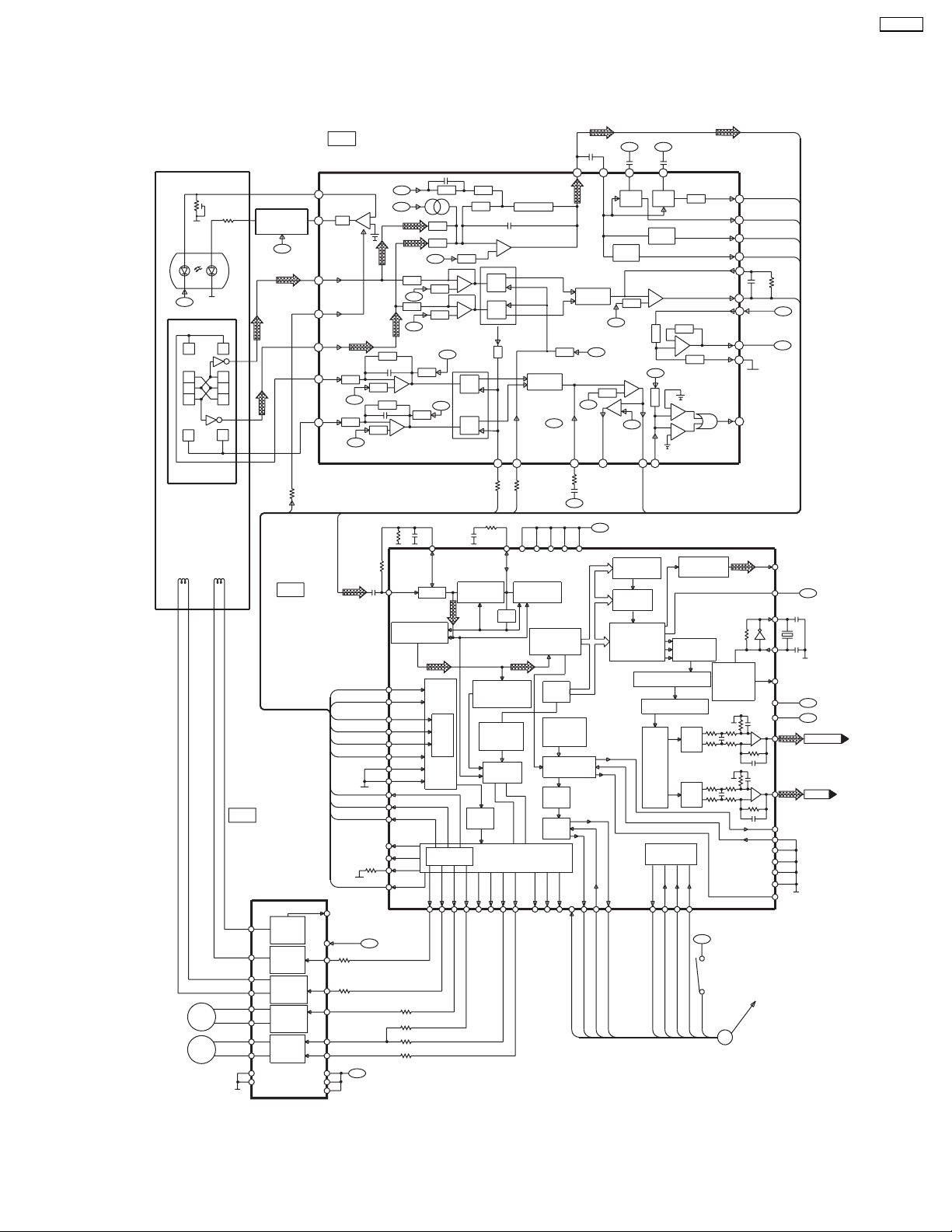
14 Block Diagram
SA-AK18
T+ T-
TRAVERSE
MOTOR
SPINDLE
MOTOR
OPTICAL PICKUP
SEMICONDUCTOR
LASER
+B
PHOTO DETECTOR
E
D
A
D
FF
FOCUSTRACKING
COIL
COIL
M
_
M
_
Q701
LASER
POWER DRIVE
+B
E
C
B
C
LDON
F-F+
IC702
MN662790RSC
SERVO PROCESSOR
/DIGITAL SIGNAL
PROCESSOR
/DIGITAL FILTER
/D/A CONVERTER
IC703
AN8739SBE2
FOCUS COIL/
TRACKING COIL/
TRAVERSE MOTOR/
SPINDLE MOTOR
DRIVE
RESET
D4+
18
SIGNAL
GEN.
FOCUS
D4-
17
COIL
DRIVE
16
D3+
TRACKING
15
D3-
COIL
DRIVE
D1+
12
TRAVERSE
11
MOTOR
D1-
DRIVE
14
D2+
SPINDLE
MOTOR
13
D2-
DRIVE
9
PGND1
20
PGND2
13
/RST
VREF
PVCC1
PVCC2
VCC
6
7
4
5
1
2
IN3
IN4
IN1
PC284
AN8839NSBE2
SERVO AMP
LPD
LD
PDA
LDON
PDB
PDE
PDF
1
24
26
25
6
3IN2
21
23
IC701
+
-
+B
+
+B
RF
44
39
BDO
38
/RFDET
34
RFENV
FE
TE
OFT 36 OFT
37
35
29
VREF
31
TBAL
30
FBAL
41
43
42
40
LDON
+B
+B
+B
+B
+B
+B
+B
+
F
47 80448
DSLF
ARF
DSL
SYNCHRONIZING
PROTECTION
BDO
SERVO
INPUT
/RF DET
PORT
RF ENV
FE3332
TE
TRCRS
VDET
VREF
TBAL
FBAL
PLLF2
WVEL
CONVERTER
DSLF2
LDON
TRD
28
+B
+B
A/D
D/A
22
A
+
B
+
Ech
VCBA
Fch
PHASE
COMPARATOR
CONVERTER
TVD27FOD
ECS
25
+
Ach
VCBA
Bch
Vref
TBAL
27
TBAL
PLLF
VCO
SYNCHRONIZING
INTERPOLATION
PROTECTION
RAM
ADDRESS
GENERATOR
CLV
SERVO
SERVO
CPU
SERVO OUTPUT
ECM
KICK
TRV23PC
24
2126
Subtracter
FBAL
28
FBAL
DV DD1
FREQUENCY
COMPARATOR
DEMODULATOR
PORT
SENSE
10 11
8
RF
+B
TEIN
22 23
+B
50
7260
SSEL
V DD
AV DD2
EFM
DATA
16K
SRAM
PEAK
DETECTOR/
AUTO CUE
SUB-CODE
DEMODULATOR
CRCC
CHECK
CRCC
CHECK
/RST
TLOCK
FLOCK
/RSTEST/DO
RFIN
Subtracter
+B
+B
AVDD1
BLKCK
1418 1312 15
BLKCK
10
9
CSBRT CEA
+B
PDOWN
16
+B
SYNDROME
CALCULATION
CIRC
DECODER
INTERPOLATION
/SOFT MUTING
ATTENUATION
SQCK
SUBQ
SUBQ
+B+B
11
OFTR
3
DET.
TENV
BDO
DET.
RF
DET.
+
+B
+
+
-
+B
TEOUT
N.C.
21
TE
/DIGITAL
DIGITAL DE-EMPHASIS
DIGITAL FILTER
MASH LOGIC
MIRCOMPUTER
INTERFACE
MDATA
STAT
879
17
MDATA
STATUS
+
+
+
DIGITAL AUDIO
INTERFACE
S/P
CONVERTER
LOGIC
PWM
PWM
LOGIC
MCLK
MLD
+B
MLD
MCLK
RESET
ENV
OFTR
BDO
/RFDET
FEN
FEOUT
VCC
VREF
GND
N.C.
TIMING
GENERATOR
/PITCH
CONTROL
S701(RESET)
19
17
12
15
/RFDET
25
24
3
26
14
18
/CLDCK
TX 6
DMUTE
SMCK
RSEL
VREF
OUTL
+
-
OUTR
+
-
SUBC
SBCK
DVSS1
CSEL
PSEL
NSEL
X1 58
+B
+B
16
59X2
19
76
29
73
75
55
56
5
20
78
79
62
RF
ENV
OFTR
BDO
FE
-B
+B
+B
CD SIGNAL
(CD SIGNAL)
X701
R CH
25
Page 26
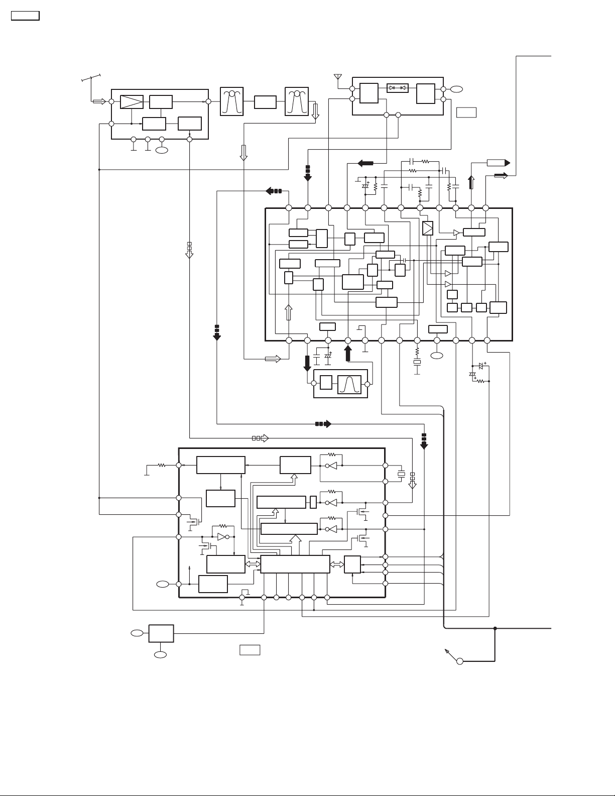
SA-AK18
This page is only applicable for GN/GT areas
FM ANT
Z120
Q1 Q2
1
RF AMP
5
MIXER
Q3
OSC
346
+B
(FM)
Q4
BUFFER
AM ANT
CF201
7
Q101
FM
IF AMP
CF202
AM
ANT
COIL
Z101
AM
OSC
COIL
+B
(FM)
IC101
LA1833NMNTLM
FM/AM IF AMP,
8
DET/AM OSC,
MIX/FM MPX
RCH
REG
PHASE
DET
VCO
FF
14
DECODER
STEREO
SWITCH
FF
13
PILOT
CANCEL
PILOT
FF
DET
24 23 22
ALC
BUFFER
LEVEL
DET
FM
IF
FM
DET
12
AM
OSC
S-CURVE
REG
3
AM
MIX
AM/FM
IF
BUFFER
4
AM
RF AMP
AM
IF
AGC
COMP
TUNING
DRIVE
SD
65
182021 19 17
AM
DET
ST
871091211
16 15
+B
Z102
AM
IFT
16
17
18
11
PHASE DETECTOR
CHARGE PUMP
UNLOCK
DETECTOR
REFERENCE
DIVIDER
SWALLOW COUNTER
1/6,1/17,4 BITS
12 BITS PROGRAMMABLE
DIVIDER
1
2
1
20
14
12
13
X102
Q305
ST/DO
SD
X103
DO
5
CE
UNIVERSAL
COUNTER
15
+B
Q106
POWER
+B
SUPPLY
CONTROL
+B
(FM:ON)
POWER ON
RESET
SHIFT REGISTER LATCH
19
710 912 6
IC102
LC72131MDTRM
PLL FREQUENCY SYNTHESIZER
C2B
I/F
8
2
3DI
4CL
ST/DO
CE
DI
CL
E
26
Page 27
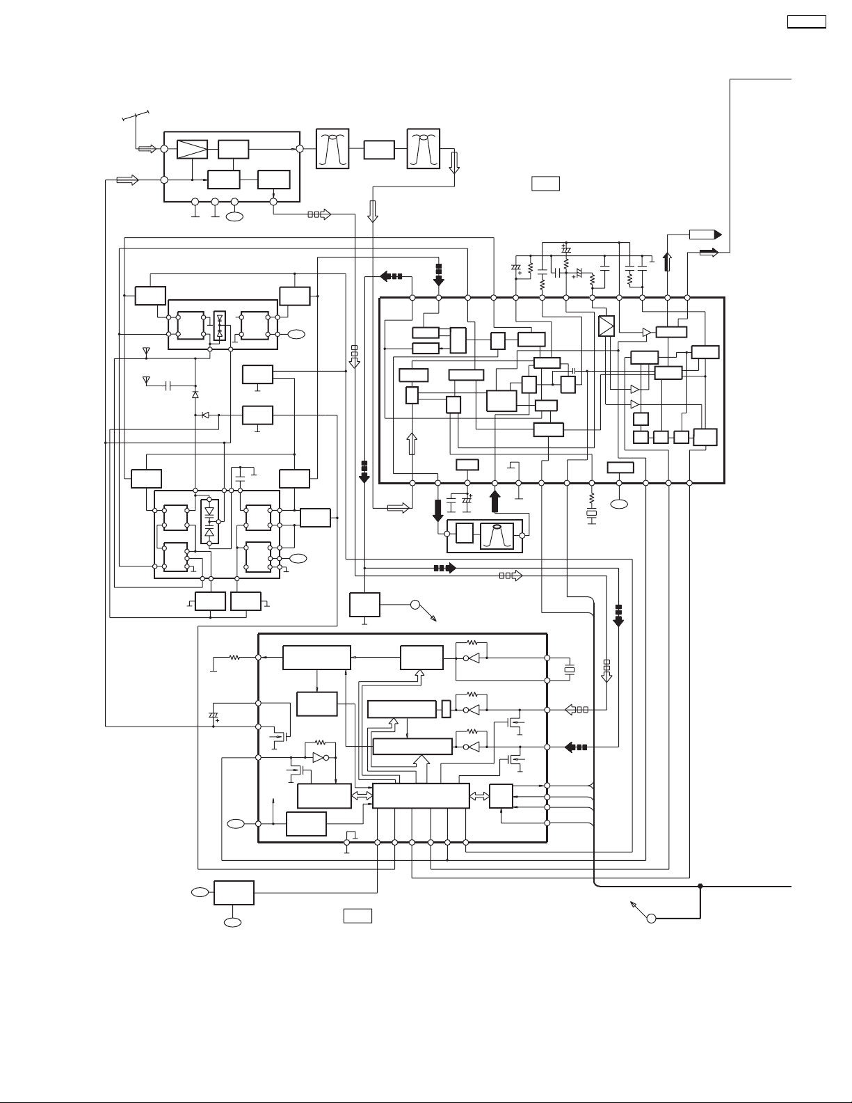
This page is only applicable for GC areas
FM ANT
Z120
Q1
1
RF AMP
5
Q2
MIXER
Q3
OSC
346
+B
(FM)
Q4
BUFFER
SA-AK18
CF201
7
8
Q101
FM
IF AMP
CF202
IC101
LA1833NMNTLM
FM/AM IF AMP,
DET/AM OSC,
MIX/FM MPX
RCH
Q152
SWITCH
AM ANT
AM EXT ANT
Q154
SWITCH
13
14
15
16
Q158
SWITCH
Q159
SWITCH
Q155
16
17
18
11
LW
OSC
COIL
SW1
OSC
MW
OSC
Q151
SWITCH
10
11
+B
Q153
SWITCH
21
20
19
18
17
PHASE DETECTOR
CHARGE PUMP
Q157
+B
UNLOCK
DETECTOR
SWITCH
Q107
MUTING
SWALLOW COUNTER
1/6,1/17,4 BITS
12 BITS PROGRAMMABLE
DIVIDER
24 23 2122
ALC
AM
OSC
BUFFER
LEVEL
DET
FM
IF
12
REFERENCE
DIVIDER
S-CURVE
FM
DET
M
1
2
REG
3
AM
IFT
Z102
AM/FM
IF
BUFFER
4
20 19 18
AM
AM
RF AMP
MIX
17
AGC
AMAM
IF
DET
COMP
TUNING
DRIVE
ST
SD
856 7
X102
ST/DO
SD
1
X103
20
14
13
Z151
5
4
1
MW
ANT
2
COIL
Z152
9
1
SW1
ANT
2
8
3
7
MW
6
ANT
4
5
3
10
12
SWITCH
986
7
11
Q156
SWITCH
1516
PHASE
DET
VCO
REG
10911
+B
14 13
DECODER
STEREO
SWITCH
PILOT
CANCEL
PILOT
FFFFFF
DET
12
DO
5
ST/DO
CE
UNIVERSAL
COUNTER
15
+B
Q106
POWER
+B
SUPPLY
CONTROL
+B
(FM:ON)
POWER ON
RESET
SHIFT REGISTER LATCH
19 10 7 12 6 9 8
IC102
LC72131MDTRM
PLL FREQUENCY SYNTHESIZER
C2B
I/F
2CE
DI
3
CL
4CL
DI
TO CD UNIT
E
27
Page 28
SA-AK18
IC1
TA7291P
MOTOR DRIVE
8
Vs
-B
REG
5
IN1
IN2
6
4
Vref
1
7
Vcc
GND
OUT1
2
OUT2
10
M
RM1
+B
STATUS
SUBQ
ST/DO
BLKCK
/CDRST
RESTSW
SD
CE/MLD
DI/MDATA
CL/MCLK
VT
Q1
POWER
SUPPLY
CONTROL
Q902
INTERFACE
A
26
MLD/PLLCE
27
MDATA/PLLDA
28
MCLK/PLLCLK
Q901
INTEFACE
Q903
INTERFACE
SD
2921
RESTSW
3018 2220
CDRST
BLKCK
SQCLK
STATUS
ST/DO/SUBQ
2319 24
CHG_CW
M38199MF227
25 17
CHG_CCW
IC600
+B
CHG_HALF
SYSTEM CONTROL/FL DRIVE
SW5
+B
SW4
CHG_AD2
SW2
SW1
SW3
16 44
CHG_AD1
43
CHG_SW1
CHG_SW2
Q350
PLUNGER
Q351
SUPPLY
DRIVER
SWITCH
SUPPLY
45
CHG_PLGR
-B
28
Page 29
SA-AK18
(DECK 1)
P.B.
HEAD
(DECK 2)
R/P
HEAD
LCH
LCH
IC1004
BA7755A
R/P SELECT
4
2
1
+B
IC1001
AN7348STA-E1
P.B. EQ /TPS AMP
REC AMP./ALC
(DECK 2)
ERASE
HEAD
3
5
Q1017
MOTOR
DRIVE
M
MOTOR
SOLENOID
D951
REC;ON/
BEAT PROOF
SWITCHING
Q1001,Q1003
IC1002
BU2090AF-E2
I/O EXPANDER
Q1023
Q1019
SOLENOID
DRIVE
(DECK 1)
24(23)
22(3)
21(4)
17(8)
Q1012(Q1013)
1(2)
+
20(5)
-
18(7)
6
19
15
12
L601
LOGIC L/H
ALC
NOR/CrO &
HI/LO LOGIC
LOGIC
REC/PB
9
+B
RIPPLE
REJECTION
BIAS OSC
CONTROL
Q1004~Q1007
10
16
14
13
11
Q1022
MUTING
(Q1015)
(Q1021)
Q1014
Q1020
Q1016
BUFFER
AMP
FILTER
AMP
SWITCH
(DMT)
IC1003
BA4558FE2
BUFFER
AMP
Q1024
TPS
DRIVE
+B
16
VCC
CONTROL
CIRCUIT
1M13
LATCH
BP17
1PL15
REGISTER
12-BIT SHIFT
GND
1
2
DATA
3
CLK
11
REC
12
CR02
1H
10
8
OUTPUT BUFFER
2PL
14
Q1018
SOLENOID
DRIVE
(DECK 2)
SOLENOID
D971
Z1002
S972
(HALF)
(MODE)
S971
(Cr02)
S973
M38199MF227
PHOTO
INTERRUPTER
INTERFACE
4
IC600
15
SW600
(VOLUME)
IC971
ON2180RLC1
(DECK 2)
(Q1008,Q1009)
DECK 2
SYSTEM CONTROL/FL DRIVE
J_JOG_A/B
S974
INTERFACE
29
(F.REC INH)
95
(R.REC INH)
S975
REG_IN
S952
(HALF)
14
VR600
JOG VOL
S953
S951
(MODE)
INTERFACE
(Q1010,Q1011)
V_JOG_A/B
(Cr02)
3
PHOTO
INTERRUPTER
DECK 1
Z1001
IC951
ON2180RLC1
(DECK 1)
2
TPS
Page 30

SA-AK18
FROM
CD UNIT
CD SIGNAL
AUX
JK305
21
(56)
(44) (54)
79(66)
IN1F VIDEO/MD
78(67)
IN1E TUNER
77(68)
IN1D TAPE PB
76(69)
IN1C CD
75(70)
IN1B EXTIN
74(71)
IN1A PHONO/AUX
18
(46)
(47)
910 11
(55)
(60)(45) (43)
(53) (52)
COMOUT1 TAPE REC1
1312
IC303
M62433AFP
AUDIO IC
VOLIN1
GEQOUT1
2319 20 225
(42)
14 15
(51) (50)
AVDD
36
+B
SWITCH
(LEVEL 3DAI)
Q304
(49)
VOLOUT
KARA/LINE_MUT PORT B
AI3D PORTA
DELIN
PS-IN
DGND
BPIN
658029
16135
BUFIN
BUFNF
BUFOUT
DVDD
DATA
LATCH
MICIN
CLK
26
(39)
25
(40)
27
(38)
28
(37)
30
31
+B
32
33
34
SER2
24
17
16
(41)
(48)
IC603
M62457AFPE1
SPECTRUM ANALYZER
867
ANF
AOUT
+
A
B
10 1211 1413 1615 9
D633D635 D634
47 48
46
SPB
SPA
MBP2
42 41
X'TAL
CONTROL
Q608,Q609
CNF
+
BPF5
P.HOLD
MCU I/F
C
SPC
+
4532
COUT
DIFOUT
+
BPF4
P.HOLD
BPF3
P.HOLD
ENB
BPF2
P.HOLD
BPF1
P.HOLD
GND1
+B
MBP1
XOUT
39 38
X600
IREF
PHOUT
13
I REF GEN.
SPE
XIN
+1+
VREF
V REF GEN.
SELECTOR
GND2
VCC/2
VCC/2 GEN.
VCC
+B
XCOUT
37 36
X601
FOR GC/GT AREA ONLY
M38199MF227
XCIN
MIC
JK601
Q605,Q606
FL DRIVE
Q600,Q601
MIC AMP
IC600
+B
SYSTEM CONTROL/FL DRIVE
GRD13
GRD1
49~61
FL DISPLAY
FL901
10
SEG32
62~90,92~94
SER2
SEG1
1
12 11
SER4
SER5
FROM
POWER
TRANSFORMER
SER3
30
Page 31

SA-AK18
Q401(Q201)
MUTING
Q309
LEVEL
VBASS
LVL/VBASS
M
FOR GC
AREA ONLY
MUTEA
Q400(Q200)
MUTING
Q306
MUTING
CONTROL
IC302
M5218AP
BUFFER
AMP
HP_L(R)
HP_L(R)
DCDET
SER2
2
3
16
+B
1
IC601
BU2090AF-E2
I/O EXPANDER
DATA
CLK
VCC
GND
CONTROL
CIRCUIT
VBASS
MUTE_A
PLY_TIM
LATCH
LED_CTL
OUTPUT BUFFER
12-BIT SHIFT REGISTER
PCONT 7
3D_AI
REC/
6
8
5
10
11~15G5~G1
/CD
4
9
LVL/VBASS
Q602
POWER
SUPPLY
MUTEA
+B
+B
+B
+B
/CD
SYNC
/CD
A
KEY SW
5~8
KEY4
KEY1
M38199MF227
Q607
CONTROL
35
RESET
/RESET
SWITCH
Q311
DETECTOR
Q307
SWITCH
+B
(COMPARATOR)
9
SER1
IC600
SYSTEM CONTROL/FL DRIVE
+B
Q352
DC
Z602
D313
PCONT
DCDET
PCONT
+B -B -B
32
DCDET
RMT
31
100 98
VREF
VSS
40
VEE
99
AVSS
SYNC
ECONO
34
33
SYNC
31
Page 32

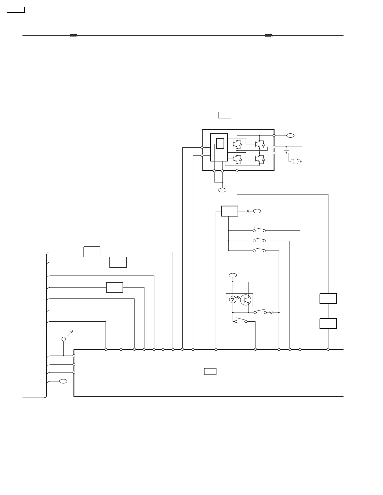
SA-AK18
9
11(13)
10(14)
Q502(Q500)
SWITCH
Q504,Q505
DETECTOR
IC500
RSN3502B
POWER (HIC)
+B
23
+INL(R)
+
-INL(R)
-
DC
OUT L(R)
Q503
SWITCH
(AGC)
-B
AC IN
IC501
STK470-010A
REGULATOR
14
+B
13
D508
12
11
+
7
+
8
-B
4(1)
6
LCH
SPEAKER
LCH
(6 Ω)
+
-
15
+B
16
17
18
-B
19
10
-B
9
8
+
7
6
+B
5
+B
4
3
+B
2
1
+B
+
Q510
BIAS SWITCH
(FOR CD 3.3V)
Q509
SUPPLY
SWITCHING
(CD)
JK600
HEADPHONE
Rch
Q611
POWER
SUPPLY
CONTROL
Q610
POWER
SUPPLY
SIGNAL LINES
MAIN SIGNAL LINE
FM OSC SIGNAL LINE
FM SIGNAL LINE
( ) indicates Pin No. of right channel.
Q507
SWITCH
(HEADPHONE)
+B
Q511
CD SIGNAL LINE
AM OSC SIGNAL LINE
MIC SIGNAL LINE
RELAY
DRIVE
+B
D512
Q508
-B
D527,
D529~D535
SWITCH
(PCNT)
Q501
REGULATOR
TO
FL DISPLAY
AM SIGNAL LINE
FM & AM SIGNALS LINE
AUX SIGNAL LINE
D507~D510
RL500
FOR GC AREA ONLY
Q976
REGULATOR
+B
Q977
+B
REGULATOR
T501
POWER TRANSFORMER
Q978
SWITCH
E500
D979,D980
+B
D977
RL502
Z501
FOR GC/GT AREA ONLY
T502
S501
VOLTAGE
SELECTOR
F2
Q975
RELAY
DRIVE
JK500
AC IN
F1
PLAYBACK SIGNAL LINE
RECORD SIGNAL LINE
32
Page 33

15 Schematic Diagram
SA-AK18
(All schematic diagrams may be modified at any time with the
development of the new technology)
Note:
S501 Voltage selector switch
S701 Reset switch
S602 AUX select switch
S603 Deck 1 eject switch
S604 CD Manager switch
S605 Band/Tuner select switch
S606 Tape Edit switch
S607 Disc 5 eject switch
S608 CD select switch
S609 Rec/Stop select switch
S610 Disc 5 select switch
S611 Tape/Deck select switch
S612 Reverse Mode select switch
S613 Disc 4 eject switch
S614 EQ adjust down switch
S615 V.Bass switch
S616 Deck 2 eject switch
S617 Disc 4 select switch
S618 EQ adjust left switch
S619 Display, Demonstration switch
S620 Reverse play, Tune/time adjust down
switch
S621 Clock, Timer select switch
S622 EQ adjust up switch
S623 Disc 3 eject switch
S624 Karaoke select switch
S625 Play timer/Rec timer select switch
• The voltage value and waveforms are the reference voltage of this unit measured by DC electronic voltmeter (high impedance)
and oscilloscope on the basis of chassis. Accordingly, there may arise some error in voltage values and waveforms depending
upon the internal impedance of the tester or the measuring unit.
No mark : Playback << >> : Rec <>:FM (( )) : CD ():AM
S626 EQ adjust right switch
S627 Disc 3 select switch
S628 Economy Mode switch
S629 Stop,Tune Mode select switch
S630 Disc 2 eject switch
S631 Random play switch
S632 FWD, Memory set switch
S633 Disc 2 select switch
S634 FWD play/pause, Tune/Time adjust up
switch
S635 Disc 1 eject switch
S636 Disc 1 select switch
S637 REW, FM Mode/BP select switch
S638 Power switch
S639 3D AI EQ switch
S951 Deck 1 Mode detect switch
S952 Deck 1 Tape detect switch
S953 Deck 1 CrO2 detect switch
S971 Deck 2 Mode detect switch
S972 Deck 2 Tape detect switch
S973 Deck 2 CrO2 detect switch
S974 Deck 2 Record detect switch
S975 Deck 2 Record detect switch
SW1, SW2 Tray position switch
SW3 Tray open switch
SW4 CD offset detect switch
SW5 Spindle bottom position detect switch
SW600 Sound Equalizer select switch
VR600 Volume control
VR601 MIC level control
• Importance safety notice:
Components identified by
purposes of fire-retardant (resistors), high-quality sound (capacitors), low-noise (resistors), etc. are used. When replacing any
of components, be sure to use only manufacturer´s specified parts shown in the parts list.
Caution!
IC, LSI and VLSI are sensitive to static electricity.
Secondary trouble can be prevented by taking care during
repair.
mark have special characteristics important for safety. Furthermore, special parts which have
• Cover the parts boxes made of plastics with aluminium foil.
• Put a conductive mat on the work table.
• Ground the soldering iron.
• Do not touch the pins of IC, LSI or VLSI with fingers directly.
33
Page 34

SA-AK18
SCHEMATIC DIAGRAM-1
OPTICAL PICKUP
CIRCUIT
LASER DIODE
6
8
11
12
4
9
10
5
2
3
3
2
1
4
AIN
BIN
VCC
GND
VREF
NBOUT
GND
NAOUT
8
5
6
7
TRACKING
COIL
FOCUS
COIL
: + B Line
: CD Signal Line
CD SERVO CIRCUIT
PLAY
0.6V
0.5us. 0.2V/DIV
C714
6.3V100
PLAY
2ms 0.1V/DIV
C712
0.1
C711
P-P
3.2V
1.6V
1.6V
1.6V
PDF
PDE
VCC
PDA
TBAL
VREF
FEN
FBAL
26
27
25
1.6V
1.6V
1.6V
1.6V
0.1V
P-P
0.1
R708
22K
R707
39K
C747
180P
R744
120K
C749
2200P
C701
6.3V33
R701
4.7
Q701
2.7V
CN701
VCC
1
1
PDF
2
2
PDE
3
3
LD
4
4
LD GND
5
5
GND
6
6
NB
7
7
GND
(GUARD)
8
8
NA
9
9
VREF
10
10
LPD
11
11
GND
(GUARD)
12
12
T-
13
13
T+
14
14
F-
15
15
F+
16
16
3.2V
C713
0.1
C750
0.1
C751
0.9V
((2V))
0.1
Q701
((2.3V))
2SA1037AKSTX
LASER POWER
DRIVE
701
J
RF
29
0.1
C702
1.6V
0.9V ((1.4V))
1.9V
0V ((0.2V))
0.7V
2.7V ((2.3V))
98
7654321
LD
RF
LPD
PDB
FEOUT
TEOUT
23
1.6V
C710
120P
R702
C742
0.027
R706
1K
RFIN
TEN
NC
NC
21
2228
20 19
1.6V
R705
150K
10K
R704
1K
IC701
AN8839NSBE2
SERVO AMP
24
1.6V
C706 2700P
CSBRT
ENV
1.6V
C703
6.3V100
C704
0.1
0.027
C707
1.6V
121110
CEA
NC
18
17
0V
OFTR
0V
13
BDO
16
0V ((3.1V))
14
GND
LDON
/RFDET
PDOWN
15
0V
((3.2V))
2ms 0.1V/DIV
33
PLAY
42
0.6V
P-P
IC703
AN8739SBE2
FOCUS COIL/
TRACKING COIL/
TRAVERSE MOTOR/
SPINDLE MOTOR DRIVE
C735
10V220
36
38
0.1
C734
3.3V
((3V))
3.3V
((3V))
16
15
D3-
D3+
D2+
14
13
3.3V
3.3V
((3.5V))
C737
SP MOTOR
TRV MOTOR
((3.5V))
17
D2-
12
3.7V
((3.3V))
0.1
M
M702
C736
0.1
M
M701
3.3V
D1+
D4-
3.7V
3.3V
181119
D4+
D1-
((4.1V))
7.3V
10
7.3V
7.3V
7.3V
21
20
NC
GND
PGND2
PVCC2
IC703
GND
PVCC1
NC
PGND1
9
8
35
23
22
NC
VCC
NC
IN1
6
7
1.6V
R735
100
1.6V
1.6V
24
IN4
IN3
VREF
RSTIN
PC2NCIN2
NC
52542632721
3.2V
1.6V
1.6V
1.6V
((0V))
R724
18K
1.6V
28
NC
/RST
C715
2700P
R725
390
R715
1K
R727
3.9K
R736
100
R729
3.9K
C739
1500P
R728
3.9K
C752
1500P
R749
4.7K
C738
0.01
37
R723
6.8K
R731
6.8K
34
Page 35

SA-AK1
8
SCHEMATIC DIAGRAM-2
C754
470P
C723
10V220
C724
0.1
61 62
60
59
58
57
56
55
54
53
52
51
50
49
48
47
46
45
44
43
42
41
PLLF2
((3.2V))
VDD
X2
X1
VSS
SBCK
SUBC
VCOF2
PCK
EFM
AVSS2
AVDD2
VCOF
PLLF
DSLF
DRF
IREF
ARF
WVEL
DSLF2
0V
IN
40
OUT
63
BYTCK
/CLDCK
LDON
BDO
39
38 37 36 35
0V
3.2V((0V))
X701
16.9344 MHz
C722
10P
82K
R711
F=16.9344MHz
0.1
C717
C716
820P
R714
C744
C721
10P
R709
68K
0
8200P
1.6V
P-P
C718
0.22
R712
220
R741
R742
220K
3.2V
1.5V
1.5V
3.2V
0.5V
1.6V
1.6V
47K
1V
1.6V
1.5V
R721
100
6.3V220
3.2V
68
64
FCLK
IPFLAG
F=16.9344MHz
IC702
MN662790RSC
SERVO PROCESSOR
DIGITAL SIGNAL PROCESSOR/
DIGITAL FILTER/
D/A CONVERTER
0.5us 0.2V/DIV
TRCRS
/RFDET
65
66
FLAG
PLAY
OFT
0V
69
67
CRC
CLVS
DEMPH
0.7V
P-P
0.6V
P-P
TE
RFENV
VDET
34 33 32 31 30
1.6V
1.6V
1.6V
70
RESY
FE
IOSEL
TBAL
1.6V
C731
C730
0.1
3.2V
71
/TEST
PLAY
T = 13.3ms
FBAL
29 28 27 26
1.6V
2.9V
72
AVDD1
VREF
1.6V
1.5V
73
PLAY
F=75Hz
1.6V
OUTL
T = 13.3ms
FOD
: + B Line
2.9V
1.5V
74
75 76 777879
OUTR
AVSS1
3.2V
0V
PLAY
...3.2V
0V
TRD
KICK
25 24 23
1.6V
1.6V
RSEL
...3.2V
ECS
1KHz, 0dB
6.3V220
3.2V
IOVDD
0V
ECM
1.6V
R717
1K
R718
1K
PLAY
C732
PSEL
MSEL
SRDATA
DVDD1
DVSS1
MDATA
SENSE
/FLOCK
/TLOCK
BLKCK
SQCK
SUBQ
DMUTE
SMCK
TVD
PC
22
1.6V
3.2V ((0V))
3.2V
80
SSEL
BCLK
LRCK
MCLK
MLD
STAT
/RST
CSEL
21
2.2V
P-P
TX
TRV
2ms 0.1V/DIV
2ms 0.1V/DIV
10
11
12
13
14
15
16
17
18
19
20
1
2
3
4
5
6
7
8
9
PLAY
PLAY
C733
0.1
3.2V
1.6V
3.2V
0.5V
3.2V
0V
0V ((0.2V))
3.2V ((3.1V))
0V ((3.1V))
3.1V
0.1V
P-P
0.4V
P-P
: CD Signal Line
C725
1000P
C726
1000P
C743
0.1
17
11
10
9
C745
1000P
PLAY
T = 13.3ms.
18
C727
50V1
23
22
21
C728
50V1
CN702
Lch OUT
19
A.GND
C753
470P
18
17
16
15
14
13
12
11
10
9
8
7
6
5
4
3
2
1
Rch OUT
+3.3V
D.GND
LD SW
TX
+7.5V
P.GND
MCLK
M DATA
MLD
(SPEED)
BLKCK
SQCK
SUBQ
STAT
/RST
REST SW
TO
PANEL CIRCUIT
(CP606) ON
SCHEMATIC
DIAGRAM-10...GC
SCHEMATIC
DIAGRAM-11...GN
12
8
7
...3.2V
0V
REST SW
S701
6
4
3
1
R753
10
PLAY
T = 13.3ms.
3.2V
0V
(Vref)
J
702
15
16
35
Page 36

SA-AK18
SCHEMATIC DIAGRAM-3
: FM Signal Line: +B : AM Signal Line
: FM OSC Signal Line : AM OSC Signal Line
FM EXT ANT
75
GND
AM LOOP
ANT
AM EXT
ANT
JK101
MAIN/TUNER CIRCUIT
TUNER PACK CIRCUIT
Q1
2SK544F-AC
5.6P
1
1000P
2
3
4
5
[2.5V]
(2.1V)
<2.4V>
R152
1
2
3
4
C159
Q154
[2.6V]
(2.1V)
<2.4V>
C135
0.01
R114
5.6K
C110
0.01
RF AMP
Q1
100K
100K
100K
2.7K
2.2P
Q152
R171
10K
2SA1309ARTA
SWITCHING
Q152
[2.6V]
(2.1V)
<2.5V>
[8.1V]
(8.2V)
L104
100uH
<8.2V>
33K
R156
10K
[2.6V]
(2.1V)
<2.4V>
[2V]
(1.6V)
<1.9V>
R154
68K
R139
68K
C160
0.01
(FOR GC ONLY)
Q2
2SC2786MTA
2.2P
FM MIXER
1.2u180P
3.3P
10P
0.001
4.7P
Q3
2SC2787FL1TA
LOCAL OSC
Z151 RLA3Z002-C
1
2
Q154
2SA1309ARTA
SWITCHING
Z152 RLA5Z002-C
1
2
3
4
Q156
820K
220
ANT
1K
[0V]
(0V)
<0V>
<0.1V>
390
Q3
4
5
7
3
D151
DA204KT146
C153
18P
10
11
8
12
7
6
5
[0V]
(0V)
<0V>
[0.1V]
(0.1V)
Q155
R165
4.7K 15K
Q155,Q156
2SC2412KT96R
SWITCHING
2.2P
Q4
2SC2787FL1TA
BUFFER AMP
6
560K
R157
1K
SW2 SW2 OSC
C152
22P
R158
SW1 ANT
MW ANT
Q101
2SC2058SPTA
FM IF AMP
0.001
0.47u
Q2
390390
680K
1
7
6
C101
10P
8
Q4
0.047
R168
C154
C136
1000P
910
C156
2700P
13 219
14
15
16
[0.1V]
(0V)
<0.1V>
R155
10K
R166
100K
C155
0.047
SW1 OSC
MW OSC
[0V]
(0V)
<0V>
11
20
19
18
17
(0.1V)
<0.1V>
<0V>
Q159
2SC2412KT96R
SWITCHING
8
[0V]
(0.2V)
<0V>
CF201
3
2
R103
270
C102
16V100.01
Q151
2SA1309ARTA
SWITCHING
Q159
[0V]
[0.7V]
(0.7V)
<0.7V>
[0V]
(0V)
[0V]
(0V)
<0.7V>
C104
1000P
R105
470
2
Q151
[5.4V]
(5.8V)
<5.4V>
[8.1V]
(8.2V)
<8.2V>
Q153
2SA1309ARTA
SWITCHING
Q157
2SC2412KT96R
SWITCHING
[5.3V]
<5.4V>
(5.8V)
<5.4V>
Q157
[5.9V]
(6.4V)
[5.3V]
<6V>
(5.8V)
<5.4V>
R164
22K
R162
2.2K
R169
22K
C128
1000P
[0V]
(0V)
<0V>
[0V]
(0V)
<11.5V>
R107
R106
330
470K
CF202
1
3
[5.3V]
(5.8V)
<5.4V>
R151
15K
Q153
[5.4V]
(5.8V)
[4.7V]
(5.1V)
<4.8V>
R153
15K
[0V]
(0V)
<0V>
[0V]
(0V)
<0V>
Q158
Q158
DTC114EKA146
SWITCHING
Q101
R104
1K
[5.3V]
(5.8V)
<5.4V>
[8.1V]
(8.2V)
<8.2V>
C103
0.01
R172
180K
R161
10K
C158
1000P
36
Page 37

SCHEMATIC DIAGRAM-4
8
: +B Line
: FM/AM Signal Line
Q107
R117
[3.8V]
47K
(4.3V)
[0.1V]
<4V>
[0V]
(0V)
<0V>
R119
4.7K
C127
16V22
C114
50V3.3
R108
(0.1V)
27K
<0.1V>
Q107
C105
6.3V47
DTC143XKA146
MUTING
[5.3V]
(4.3V)
<4V>
[3.9V]
(5.8V)
<5.4V>
22
2324
OSC
OSC OUT
IC101
AM MIX OUT
FM IF IN
1732456891110 12
R118
[2.1V]
3.3K
(2.1V)
<2.1V>
[5.3V]
(5.8V)
(2.1V)
[2.1V]
<5.4V>
<2.1V>
C126
10
RLI2Z020-T
Z102
2
1
3
3
6
1000P
AFC
C109
[2.5V]
REG
C106
0.01
[2.1V]
5
(2.1V)
(2.1V)
<2.4V>
4
C116
0.033
47K
C115
R120
25V4.7
(0.7V)
[0.3V]
<2.4V>
(2.1V)
[2.5V]
192021
AGC
AM RF IN
IC101
LA1833NMNTLM
FM/AM IF AMP,
DET/AM OSC,
MIX/FM MPX
GND
AM IF IN
(0V)
[0V]
(5V)
<0V>
[4.9V]
<2.1V>
C148
0.01
C147
1000P
: FM Signal Line
: FM OSC Signal Line
C120
16V10
C131
150P
C139
25V4.7
22K
R121
C119
680P
R102
4.7K
R143
22K
[0V]
<0V>
(1.2V)
<0.4V>
<2.7V>
[2.5V]
(0.6V)
<2.1V>
[2.1V]
(2.1V)
1718
AM OUT
PILOT IN
DET OUT
FM DET
ST
SD
<5V>
[3.2V]
[5.2V]
(5.2V)
[5.3V]
(4.3V)
(5.8V)
<5.2V>
<3.3V>
<5.4V>
R124
33
X102
R126
1K
R125
470
C138
0.01
R123
68K
[2.1V]
MPX IN
VCC
[3.8V]
R127
470
(2.1V)
(0V)
<2.1V>
C137
[2V]
(2.1V)
PILOT OUT
STRQ
<0V>
[3.9V]
(1.1V)
C122
50V1
R122
2.7K
3300P
<2.1V>
RCH
FM/AM
<4V>
C118
[1.8V]
[3.1V]
(1.8V)
13141516
(4V)
C117
<1.8V>
LCH
MONO
<3.2V>
0.010.01
C142
50V1
[1.8V]
(1.9V)
C123
50V1
C121
C107
4700P
: AM Signal Line
: AM OSC Signal Line
C144
R146
4700P
100K
R142
6.8K
C141
50V1
R141
6.8K
<1.9V>
R145
100K
C143
4700P
Q106
DTC114EKA146
POWER SUPPLY
(FM:ON)
Q106
[14.2V]
<14.4V>
(14.5V)
<0.1V>
[14.1V]
(14.5V)
<14.5V>
50V0.47
C129
6.3V100
C149
0.1
SA-AK1
[0V]
(0V)
R131
68
C130
6.3V100
C132
1000P
D101
UDZSTE175R1B
[2.7V]
R128
82
R132
10K
27K
R129
C113
C124
1000P
100P
(2.6V)
[0V]
[0V]
<0V>
<0V>
<0V>
<0V>
<0V>
11
12
IFIN
MONO
STRQ
FM
10
9
[14.4V]
(14.5V)
<0.1V>
<0V>
<0V>
(8.2V)
[4.6V]
<8.2V>
R133
1K
R160
8.2K
R167
1.5K
R111
C125
16V22
390
R113
10K
C111
25V4.7
R115
C112
R116
560
0.01
[14.4V]
(0V)
[0V]
<0V>
18
AOUT
IC102
DI
[0.1V]
(0.1V)
[0.1V]
<0.1V>
R1361KR1351KR134
1K
1K
[0V]
(0.9V)
[0V]
(4.9V)
<0.9V>
<5.8V>
17 16
PD
AIN
IC102
LC72131MDTRM
PLL FREQUENCY
SYNTHESIZER
CL
DO
[5.2V]
(0.1V)
(0.1V)
[0.1V]
<0.1V>
<0.1V>
470
[2.7V]
(2.7V)
<2.7V>
C133
27P
X103
C134
27P
20
XOUT
XIN
123
[2.7V]
R138
3.3K
R130
10K
(2.7V)
19
VSS
CE
<2.7V>
R137
R159
(0.9V)
(5.3V)
[5.3V]
(0V)
[0V]
<5.3V>
<0.9V>
15
14
VDD
FMIN
AM
SWA
645 78
<4V>
(5.2V)
(0.2V)
[3.9V]
(6.9V)
[6.9V]
<5.2V>
82
<6.9V>
<2.7V>
13
AMIN
SWB
[8.2V]
37
Page 38

SA-AK18
SCHEMATIC DIAGRAM-5
: +B Line : Main Signal Line
: -B Line
: Playback Signal Line
: AUX Signal Line : CD Signal Line
: FM/AM Signal Line
: Record Signal Line
: MIC Signal Line
TO
PANEL
CIRCUIT
(CP605) ON
SCHEMATIC
DIAGRAM-10
TO
DECK
CIRCUIT
(H1001/W1001)
ON SCHEMATIC
DIAGRAM-12
AUX
A GND
CDDGND
CD3.3V
CD7.5V
+7.5V
MIC G
CHG_AD1
CHG_AD2
SPCLK
SPDATA
MUTEA
PCONT
LVL1/VBASS
CN304
+15V
DGND
MO+B
MOGND
MECA.G
JK305
CN303
CDL
CDR
PGND
PBL
PBR
AGND
RECL
RECR
R401
10K
Lch
Rch
RCH
LCH
SD
DO/ST
CE
C301
1000P
1
2
3
4
5
6
7
8
9
MIC
10
11
12
SD
13
14
15
16
CD
17
18
19
20
10
9
8
7
6
5
4
3
2
1
C401
100P
C201
100P
R201
10K
R210
R410
R454
10K
112mA
75-700mA
3.9K
C402
R402
100P
3.9K
C202
100P
R202
CLA=276mV
MUTEA
302
ST_DO
CHG_AD1
CHG_AD2
SD
PLLCK
PLLCE
CD3.3V
CD7.5V
+7.5V
SPCLK
SPDATA
MUTEA
PCONT
MO10V
+7.5V
PLLDA
CDL
CDR
MIC
SD
LVL1
PBL
PBR
15V
TUNERL
R207
1.5K
PBR
10K
C204
220P
R208
-7.0V
R303
10
301
R407
1.5K
PBL
10K
220P
C404
R408
15V
CDR
CDL
CD
1K
R209
47K
1K
R409
47K
C300
0.01
R300
4.7K
SPEANA
R233
R307
180K
10K
R433
180K
C305
R301
0V((0V))
1500P
22K
R305
10K
0V((0V))
<0V>
65
R302
C306
18K
50V0.1
66
0V((0V))
<0V>
67
0V((0V))
<0V>
68
0V((0V))
<0V>
69
70
0V((0V))
80mV
<0V>
71
-7.5V((-7.5V))
<-7.5V>
72
0V((0V))
C304
<0V>
10V330
R412
R212
4.7K
4.7K
R211
2.2K
((0V))
<0V>
73
0V((0V))
<0V>
74
75
0V((0V))
<0V>
76
0V((0V))
<0V>
77
0V((0V))
<0V>
78
79
0V((0V))
<0V>
80
R308
3.3K
0V((0V))
<0V>
R306
1.2K
R344
R309
10K
3.3K
0V
0.1V
((0.1V))
<0.1V>
0V
Q304
((0V))
<0V>
R411
2.2K
MIC
R310
C308
1K
0.047
C207
50V1
<0V>
BPIN
BPOUT
IN2F VIDEO/MD
IN2E TUNER
IN2D TAPE PB
IN2C CD
IN2B EXTIN
IN2A PHONO/AUX
AVSS
AGND
IN1A PHONO/AUX
IN1B EXTIN
IN1C CD
IN1D TAPE PB
IN1E TUNER
IN1F VIDEO/MD
DELIN
PS-IN
1
R304
22K
0V((0V))
0V((0V))
<0V>
<0V>
6364 6162 5960 5758 5556 54 5253 5051 464849 47 4445 43 4142
KIN2
MICIN
KOUT2
REC2A
COMOUT2
EXT REC2
TAPE REC2
COMOUT1 TAPE REC1
REC1A EXT REC1
KOUT1
PS+IN
KIN1
23456789101112131415161718192021222324
<0V>
<0V>
0V((0V))
0V((0V))
50V1
C407
C307
1000P
D311
1SS355TE17
Q304
KTC3875GRTA
SWITCHING
(LEVEL 3DAI)
C208
0.056
0V((0V))
<0V>
DPL2
REC2B
VCR REC2
IC303
IC303
M62433AFP
AUDIO IC
DPL1
REC1B VCR REC1
<0V>
<0V>
0V((0V))
0V((0V))
C408
0.056
R213
39K
R215
1K
C209
50V0.15
0V((0V))
<0V>
<0V>
0V((0V))
C409
50V0.15
0V((0V))
<0V>
<0V>
0V((0V))
C210
0.022
0V((0V))
<0V>
0V((0V))
C410
0.022
<0V>
C211
0.039
0V((0V))
<0V>
<0V>
0V((0V))
C411
0.039
R413
39K
R415
1K
0V((0V))
<0V>
<0V>
0V((0V))
C212
0V((0V))
C412
0.022
<0V>
<0V>
0V((0V))
0.022
C213
3300P
0V((0V))
<0V>
<0V>
0V((0V))
C413
0V((0V))
0V((0V))
3300P
C214
C215
2200P
0V((0V))
0V((0V))
<0V>
<0V>
AUX SENS 263mV
AUX SENS 263mV BUFOUT1
<0V>
<0V>
0V((0V))
0V((0V))
C414
C415
2200P
2700P
<0V>
<0V>
2700P
C216
1500P
0V((0V))
0V((0V))
<0V>
<0V>
0V((0V))
0V((0V))
C416
C217
0.033
0V((0V))
0V((0V))
<0V>
<0V>
<0V>
VOLOUT2
VOLIN2
BUFIN2
GEQOUT2
BUFNF2
BUFOUT2
LATCH
PLLCE PORTB
AI3D PORTA
BUFNF1
BUFIN1
VOLIN1
VOLOUT1
GEQOUT1
<0V>
<0V>
<0V>
0V((0V))
0V((0V))
C417
0.033
1500P
AVDD
DGND
DATA
DVDD
50V0.15
0V((0V))
<0V>
CLK
C418
50V0.15
C218
40
39
38
37
36
35
34
33
32
31
30
29
28
27
26
25
0V((0V))
<0V>
0V((0V))
<0V>
0V((0V))
<0V>
0V((0V))
<0V>
7.6V((7.6V))
<7.6V>
0V((0V))
<0V>
5V((5V))
<5V>
0V((0V))
<0V>
0V((0V))
<0V>
5.2V((5.2V))
<5.2V>
0V((7.5V))
<7.5V>
0V((0V))
<0V>
0V((0V))
<0V>
0V((0V))
<0V>
0V((0V))
<0V>
0V((0V))
<0V>
C220
1000P
C420
1000P
R418
3.3K
50V22
C223
50V22
R218
3.3K
C222
470P
R216
5.6K
R416
5.6K
C423
40mA
+7.5V
R321
2.7
C312
0.1
R217
68K
C221
0.056
R456
4.7K
R453
4.7K
C421
0.056
C422
470P
R417
68K
38
Page 39

SCHEMATIC DIAGRAM-6
8
: +B Line
: -B Line
SA-AK1
: Main Signal Line
C314
C315
150P
R322
C313
0.1
D302
UDZSTE175R1B
C316
150P
150P
R455
10K
R452
10K
1SS355TE17
CN301
PGND
1
GND2
2
+7.5V
3
-7.0V
4
5
6
CD7.5V
7
CD3.3V
8
SW5V
9
-VP
10
LED9V
11
10V
12
CN300
TGND
1
15V
2
SIG_INL
3
SIG_INR
4
LO_OUT
5
GND1
6
7
8
CD
9
DC_DET
10
PCONT
11
HP_SW
12
TO
POWER
CIRCUIT
(CP500) ON
SCHEMATIC
DIAGRAM-13
TO
POWER
CIRCUIT
(CP501) ON
SCHEMATIC
DIAGRAM-13
C232
3300P
R226
0V ((0V))
<0V>
100
R426
<7.5V>
100
7.5V((7.5V))
IC302
M5218AP
BUFFER AMP
C432
3300P
HPL
R449
R448
SIG_INR
C242
50V1
C237
1000P
C437
1000P
SIG_INL
C442
50V1
+7.5V
MUTEA
LVL1/VBASS
39
+7.5V
-7.0V
39
CD7.5V
CD3.3V
SW5V
-VP
LED9V
R312
D306
DAP202KT146
6.8V
((6.9V))
<6.8V>
C331
50V4.7
4.1V
((4.1V))
<4.1V>
0V
((0V))
<0V>
0V
((0V))
<0V>
D307
DAP202KT146
10V
((10V))
<10V>
10V
((10V))
<10V>
R350
1K
10V
((10V))
<10V>
2.2
R313
39K
R316
15K
4.1V
((4.1V))
<4.1V>
R349
10K
Q351
Q350
2SB621ARSTA
SWITCHING
(PLUNGER SUPPLY)
D309
D313
1SS355TE17
Q307
KRC111STA
COMPARATOR
SWITCH
Q311
KRC111STA
DC DETECTOR
Q352
KRA102STA
SWITCHING
15V
SIG_INL
SIG_INR
CD
PCONT
HP_SW
MO10V
-7.0V
D308
1SS355TE17
5V
5V
((5V))
<5V>
0V
((0V))
<0V>
Q352
R317
1K
D312
RLN4003S-P
Q307
0V
((0V))
<0V>
D316
RL1N4003S-P
DC_DET
((5V))
Q311
VREF+
<5V>
Q350
CHG_PLGR
0V
((0V))
<0V>
Q351
KRC102STA
DRIVER SWITCH
(PLUNGER)
R249
39
R248
39
R224
R225
3.3K
15K
C229
C230
100P
47P
0V((0V))
0V((0V))
<0V>
<0V>
243
6578
0V((0V))
<0V>
C430
C429
47P
100P
R424
15K
1.8V
((1.8V))
<1.8V>
0V
Q309
((0V))
KRA102STA
<0V>
LEVEL/VBASS
HPR
1
<0V>
0V((0V))
SPCLK
SPDATA
SPLATCH
270
R323
2.2K
R324
2.2K
R325
2.2K
C236
0.47
R220
100K
50V10
50V0.22
C438
50V0.22
C233
50V10
R420
100K
C433
R236
2.2K
C238
R436
2.2K
Q200,Q400
KTD1304TA
MUTING
0V
((0V))
<0V>
Q200
0V
((0V))
<0V>
0V
((0V))
<0V>
Q400
0V
((0V))
<0V>
R326
68K
0V
((0V))
<0V>
Q201
0V
((0V))
<0V>
0V
((0V))
<0V>
Q401
0V
((0V))
<0V>
Q201,Q401
KTC3199GRTA
MUTING
C225
50V3.3
C425
50V3.3
-2.5V
((-2.5V))
<-2.5V>
-2.5V
((-2.5V))
<-2.5V>
0.7V
((0.7V))
<0.7V>
0.7V
((0.7V))
<0.7V>
-7.0V
25mA
C228
16V10
C227
680P
47K
4.7K
R223
R222
-7.4V
((-7.4V))
C329
0.1
<-7.4V>
0.01
0.068
C226
C318
R423
C330
50V1
R360
150K
R360
150K
47K
680P
C427
0V((0V))
<0V>
C428
16V10
R425
3.3K
Q306
KRA102STA
MUTING CONTROL
Q309
1.7V
((1.7))
<1.7V>
IC302
C426
0.068
4.7K
R422
C320
0.01
0.1V
((0.1V))
<0.1V>
0V
((0V))
<0V>
R221
1K
R421
1K
C317
50V1
R327
150K
-2.5V
((-2.5V))
<-2.5V>
Q306
R228
1K
R428
1K
R361
68K
8V
CHG_AD1
CHG_CCW
CLAMP
CHG_CCW
R353
R355
VREF+
10K
R358
22K
12K
R354
SW1
OPEN
TO
MOTOR
CIRCUIT
(CN1) ON
SCHEMATIC
DIAGRAM-15
CHG_CW
CHG_HALF
14
13121110987654321
CN309
CHG_CW
CHG_HALF
SW1
47K
PGND
VREF+
SW2
R359
SW2
47K
DGND
SW5V
5V
CHG_AD2
R345
220
POSITION
R346
VREF+
22K
BOTTOMSW
R351
10K
12K
R347
PLUNGER
HPR
HP_SW
26 25 2324 2122 20 13161819 17 15 14 1012 11 897
SW2
HPL
HPR
HP_SW
HP GND
-VP
LVL2
GND2
TO
PANEL
CIRCUIT
(CP604) ON
SCHEMATIC
DIAGRAM-10
SPLATCH
SW1
SPLATCH
ST_DO
ST_DO
CHG_CW
CHG_CW
CHG_CCW
CHG_CCW
CHG_HALF
CHG_HALF
PLLCE
PLLCE
PLLDA
PLLDA
PLLCK
PLLCK
DC_DET
SW1
-VP
HPL
SW2
39
SW5V
VREF+
DC_DET
CHG_PLGR
564231
SW5V
VREF+
CHG_PLGR
SPEANA
SPEANA
LED9V
ED9V
D314
RL1N4003S-P
CN302
Page 40

SA-AK18
SCHEMATIC DIAGRAM-7
: +B Line
: FM/AM Signal Line
: FM Signal Line
: FM OSC Signal Line
: AM Signal Line
: AM OSC Signal Line
FM EXT ANT
75
GND
AM LOOP
ANT
AM EXT
ANT
JK101
MAIN/TUNER CIRCUIT
TUNER PACK CIRCUIT
1
1
2
3
2
4
5
3
4
L102
1uH
AM ANT COIL
2
1
R110
1K
C114
C136
1000P
R119R118
4.7K
3.3K
C129
6.3V100
C130
6.3V100
C132
1000P
D101
UDZSTE175R1B
C133
27P
(2.6V)
<2.6V>
X103
C134
27P
R138
3.3K
R130
10K
R152
0
50V3.3
C127
2.6V
16V22
C110
5.6P
100K
2.7K
9
C107
0.047
C109
R114
5.6K
0.01
20 19
XOUT
XINDICE
2.6V
(2.6V)
Q1
2SK544F-AC
RF AMP
100K
100K
3
87
R112
100K
1000P
2.1V
(2.1V)
<2.1V>
Z102
2
1
3
C125
16V22
R113
10K
C112
0.01
0V(0V)
<0V>
18
VSS
IC102
2341
0V
(0V)
<0V>
<2.6V>
Q1
0.001
4.7P
2.2P
8
AM OSC COIL
Z101
(4.3V)
3.9V
24 23
OSC OUT
FM IF IN
12
5.4V
RLI2021M-T
R111
390
C111
25V4.7
R115
560
13.5V
(1.1V)
<13.5V>
17
AOUT
0V
(0V)
<0V>
2.2P
1.2u
180P
220
560K
Q3
2SC2787FL1TA
LOCAL OSC
Q3
4
5
6
RLA2Z007-T
C108
8P
5.4V
<4V>
<5.4V>
(5.8V)
2.6V
(2.1V)
22
21 20
AFC
OSC
IC101
AM MIX OUT
REG
2.1V
2.1V
(5.8V)
(2.1V)
(2.1V)
<5.4V>
<2.1V>
C126
3
4
6
5
R116
1K
0V(1V)
<0V>
(1V)
0V
<0V>
1516
PD
AIN
IC102
LC72131MDTRM
PLL FREQUENCY
SYNTHESIZER
CL
DO
0V
(0V)
5.1V
<0V>
<5V>
(5.1V)
R134R136R137
R135
1K1K1K 470
(FOR GN ONLY)
Q2
2SC2786MTA
FM MIXER
3.3P
10P
820K
390
2.2P
Q4
2SC2787FL1TA
BUFFER AMP
R143
22K
R120
C115
47K
25V4.7
(0.7V)
<0.4V>
0.3V
2.6V
<2.5V>
(2.1V)
<2.5V>
AGC
AM OUT
IC101
AM RF IN
LA1833NMNTLM
FM/AM IF AMP,
DET/AM OSC,
MIX/FM MPX
AM IF IN
GND
SD
534 76
0V
5V
(0V)
(5V)
<0V>
<5V>
<2.1V>
C106
0.0110
C147
1000P
C148
0.01
R151 82
R117
47K
C113
1000P
(0V)
(5.1V)
5.1V
0V
<0V>
2.6V
<2.6V>
14
13
VDD
FMIN
AMIN
AM
LW
SDL
8109657
0V
(0V)
3.8V
3.8V
<0V>
(0.1V)
<3.9V>
Q2
0.47u
390
0.001
390
10P
680K
Q4
C120
16V10
C131
150P
C139
25V4.7
C119
680P
22K
R121
R102
C116
4.7K
0.033
<0V>
(1.2V)
0V
<2.5V>
(2.5V)
2.4V
2.1V
171918
PILOT IN
DET OUT
FM DET
ST
8 9 10 11 12
5.2V
3.2V
(5.2V)
(4.3V)
<5.2V>
<3.3V>
R124
33
X102
R125
470
R126
1K
C149
0.1
R128
82
27K
R129
R132
10K
C124
100P
0V
(0V)
(2.6V)
<0V>
0V
<2.5V>
(0V)
1112
IFIN
MONO
STRQ
FM
0.3V
(13.5V)
4.2V
<0V>
(4.2V)
(4.2V)
<3.9V>
<4.2V>
R133
1K
2SC2058SPTA
7
6
8
<2.1V>
(2.1V)
2.1V
MPX IN
VCC
5.4V
(5.8V)
<5.4V>
R127
470
<0V>
Q101
FM IF AMP
1
C101 C102
0.01
C138
0.01
R123
68K
(2.1V)
<2.1V>
(0V)
3.8V
<0V>
CF201
2
16V10
<2.1V>
(2.1V)
2.1V
14 131516
PILOT OUT
STRQ
3.9V
<4V>
(1.1V)
C122
50V1
R122
2.7K
3
R103
270
C137
1.7V
RCH
FM/AM
3.1V
1000P
R105
470
0.01
C118
C142
50V1 6.8K
3300P
<1.8V>
(1.8V)
LCH
MONO
(4V)
<3.2V>
<0.7V>
C104
(1.9V)
1.8V
C121
50V0.47
0V
(0V)
R106
470K
CF202
2
0.01
C117
R142
R141
C141
50V1
Q106
KRA102MTA
POWER SUPPLY
(FM:ON)
<1.9V>
50V1
C123
R146
6.8K
(13.6V)
1
3
100K
13.6V
<0V>
R145
100K
0V
(0V)
<0V>
0V
(0V)
<11.5V>
C144
(13.6V)
<13.6V>
Q106
R107
6800P
13.6V
330
R104
C143
6800P
1K
Q101
0V
(0V)
<13.5V>
C103
0.01
R131
68
40
Page 41

A
SCHEMATIC DIAGRAM-8
8
: +B Line : Main Signal Line
: -B Line
MAIN/TUNER CIRCUIT
: Playback Signal Line
: AUX Signal Line : CD Signal Line
SA-AK1
: FM/AM Signal Line
: Record Signal Line
TO
PANEL
CIRCUIT
(CP605) ON
SCHEMATIC
DIAGRAM-11
TO
DECK
CIRCUIT
(H1001/W1001)
ON SCHEMATIC
DIAGRAM-12
AUX
CN303
A GND
CDDGND
CD3.3V
CD7.5V
PGND
+7.5V
MIC G
CHG_AD1
CHG_AD2
SPCLK
SPDATA
MUTEA
PCONT
LVL1/VBASS
CN304
AGND
RECL
RECR
+14V
DGND
MO+B
MOGND
MECA.G
JK305
CDL
CDR
PBL
PBR
R401
10K
Lch
Rch
RCH
LCH
DO/ST
SD
CE
C301
1000P
1
2
3
4
5
6
7
8
9
MIC
10
11
12
SD
13
14
15
16
CD
17
18
19
20
10
9
8
7
6
5
4
3
2
1
C401
100P
C201
100P
R201
10K
R210
1K
R410
1K
R454
10K
C300
R300
4.7K
112mA
75-700mA
3.9K
C402
R402
100P
3.9K
C202
100P
R202
CLA=276mV
302
TUNERL
30%MOD=120mV
R207
1.5K
R209
47K
R409
47K
ST_DO
SD
0.01
+7.5V
15V
PLLCK
PLLDA
PLLCE
CDL
CDR
CD3.3V
CD7.5V
+7.5V
MIC
CHG_AD1
SD
CHG_AD2
SPCLK
SPDATA
CD
MUTEA
PCONT
LVL1
PBL
PBR
15V
MO10V
PBR
CLA=276mV
301
PBL
CDR
CDL
CLA=215mV
10K
C204
220P
R208
R407
1.5K
10K
C404
220P
R408
SPEANA
R233
R307
220K
10K
R433
220K
MIC=1.3V
CD0dB=1.58V
C305
R301
0V((0V))
1500P
22K
R305
10K
0V((0V))
<0V>
65
R302
C306
18K
50V0.1
66
0V((0V))
<0V>
67
0V((0V))
<0V>
68
0V((0V))
<0V>
69
70
0V((0V))
80mV
<0V>
71
-7.5V((-7.5V))
<-7.5V>
72
0V((0V))
<0V>
73
C304
0V((0V))
10V330
<0V>
74
75
0V((0V))
<0V>
76
0V((0V))
<0V>
77
0V((0V))
<0V>
78
79
0V((0V))
<0V>
80
R308
3.3K
0V((0V))
10
R303
R412
R212
4.7K
4.7K
R211
2.2K
<0V>
R306
1.2K
R344
R309
10K
3.3K
0V
0.1V
((0.1V))
<0V>
((0V))
<0.1V>
0V
Q304
((0V))
<0V>
-7.0V
R411
2.2K
MIC
R310
C308
1K
0.047
C207
50V1
<0V>
BPIN
BPOUT
IN2F VIDEO/MD
IN2E TUNER
IN2D TAPE PB
IN2C CD
IN2B EXTIN
IN2A PHONO/AUX
AVSS
AGND
IN1A PHONO/AUX
IN1B EXTIN
IN1C CD
IN1D TAPE PB
IN1E TUNER
IN1F VIDEO/MD
DELIN
PS-IN
1
R304
22K
0V((0V))
0V((0V))
<0V>
<0V>
6364 6162 5960 5758 5556 54 5253 5051 464849 47 4445 43 4142
KIN2
MICIN
KOUT2
REC2A
COMOUT2
EXT REC2
TAPE REC2
COMOUT1 TAPE REC1
REC1A EXT REC1
PS+IN
KIN1
KOUT1
23456789101112131415161718192021222324
<0V>
<0V>
0V((0V))
0V((0V))
50V1
C407
C307
1000P
D311
1SS355TE17
Q304
KTC3875GRTA
SWITCHING
(LEVEL 3DAI)
C208
0.056
0V((0V))
DPL2
REC2B
VCR REC2
IC303
IC303
M62433AFP
AUDIO IC
DPL1
REC1B VCR REC1
<0V>
<0V>
0V((0V))
0V((0V))
C408
0.056
CLA=480mV
R213
39K
CD-0dB=1.58V
20mV
30.6mV
R215
1K
<0V>
C209
50V0.15
0V((0V))
<0V>
<0V>
0V((0V))
C409
50V0.15
0V((0V))
<0V>
<0V>
0V((0V))
C210
0.022
0V((0V))
<0V>
<0V>
0V((0V))
C410
0.022
C211
0.039
0V((0V))
<0V>
<0V>
0V((0V))
C411
0.039
R413
39K
R415
1K
0V((0V))
<0V>
<0V>
0V((0V))
C212
0V((0V))
0V((0V))
C412
0.022
<0V>
<0V>
0.022
C213
0V((0V))
0V((0V))
3300P
0V((0V))
<0V>
<0V>
<0V>
0V((0V))
C413
3300P
<0V>
AUX SENS 263mV
C214
C215
2200P
0V((0V))
0V((0V))
<0V>
AUX SENS 263mV BUFOUT1
<0V>
0V((0V))
0V((0V))
C414
C415
2200P
2700P
<0V>
<0V>
2700P
C216
0V((0V))
0V((0V))
1500P
<0V>
<0V>
0V((0V))
0V((0V))
C416
C217
0.033
0V((0V))
0V((0V))
<0V>
<0V>
VOLOUT2
VOLIN2
BUFIN2
GEQOUT2
BUFNF2
BUFOUT2
PLLCE PORTB
AI3D PORTA
BUFNF1
VOLIN1
VOLOUT1
GEQOUT1
<0V>
<0V>
0V((0V))
0V((0V))
C417
0.033
1500P
<0V>
AVDD
DGND
LATCH
DATA
DVDD
BUFIN1
<0V>
0V((0V))
CLK
C418
50V0.15
C218
50V0.15
<0V>
40
39
38
37
36
35
34
33
32
31
30
29
28
27
26
25
0V((0V))
<0V>
0V((0V))
<0V>
0V((0V))
<0V>
0V((0V))
<0V>
7.6V((7.6V))
<7.6V>
0V((0V))
<0V>
5V((5V))
<5V>
0V((0V))
<0V>
0V((0V))
<0V>
5.2V((5.2V))
<5.2V>
0V((7.5V))
<7.5V>
0V((0V))
<0V>
0V((0V))
<0V>
0V((0V))
<0V>
0V((0V))
<0V>
0V((0V))
<0V>
C223
50V22
R218
3.3K
C222
470P
C220
1000P
R216
5.6K
R416
5.6K
C420
1000P
R418
3.3K
C423
50V22
40m
+7.5V
R321
2.7
C312
0.1
R217
68K
C221
0.056
R456
4.7K
R453
4.7K
C421
0.056
C422
470P
R417
68K
41
Page 42

SA-AK18
SCHEMATIC DIAGRAM-9
: +B Line
: -B Line
: Main Signal Line
C314
150P
50V3.3
C224
50V3.3
C315
C424
R322
270
C313
D302
UDZSTE175R1B
C316
150P
150P
R455
10K
R452
10K
R419
4.7K
1SS355TE17
CN301
PGND
1
GND2
2
+7.5V
3
-7.0V
4
5
6
CD7.5V
7
CD3.3V
8
SW5V
9
-VP
10
LED9V
11
10V
12
CN300
TGND
1
15V
2
SIG_INL
3
SIG_INR
4
LO_OUT
5
GND1
6
7
8
CD
9
DC_DET
10
PCONT
11
HP_SW
12
TO
POWER
CIRCUIT
(CP500) ON
SCHEMATIC
DIAGRAM-13
TO
POWER
CIRCUIT
(CP501) ON
SCHEMATIC
DIAGRAM-13
C232
3300P
R226
0V ((0V))
<0V>
100
R426
<7.5V>
100
7.5V((7.5V))
C432
3300P
C237
1000P
C437
1000P
LVL1/VBASS
C242
50V1
C442
50V1
HPL
R449
R448
SIG_INR
SIG_INL
+7.5V
MUTEA
39
+7.5V
-7.0V
39
CD7.5V
CD3.3V
SW5V
-VP
LED9V
R312
D306
DAP202KT146
6.8V
((6.9V))
<6.8V>
C331
50V4.7
4.1V
((4.1V))
<4.1V>
0V
((0V))
<0V>
0V
((0V))
<0V>
D307
DAP202KT146
10V
((10V))
<10V>
10V
((10V))
<10V>
R350
1K
10V
((10V))
<10V>
2.2
R313
39K
R316
15K
4.1V
((4.1V))
<4.1V>
R349
10K
Q351
Q350
2SB621ARSTA
SWITCHING
(PLUNGER SUPPLY)
D309
D313
1SS355TE17
Q307
KRC111STA
COMPARATOR
SWITCH
Q311
KRC111STA
DC DETECTOR
Q352
KRA102STA
DETECT SWITCH
(PCONT)
15V
H_OUT_L
H_OUT_R
CD
PCONT
HP_SW
MO10V
-7.0V
D308
1SS355TE17
5V
5V
((5V))
<5V>
0V
((0V))
<0V>
Q352
R317
1K
D312
RL1N4003S-P
CHG_PLGR
Q307
0V
((0V))
<0V>
D316
RL1N4003S-P
Q350
0V
((0V))
<0V>
Q351
KRC102STA
DRIVER SWITCH
(PLUNGER)
DC_DET
((5V))
<5V>
Q311
VREF+
R249
39
R248
39
R224
R225
3.3K
15K
C229
C230
100P
47P
0V((0V))
0V((0V))
<0V>
<0V>
243
6578
0V((0V))
<0V>
C430
C429
47P
100P
R424
15K
1.8V
((1.8V))
<1.8V>
0V
Q309
((0V))
KRA102STA
<0V>
LEVEL/VBASS
HPR
1
<0V>
0V((0V))
IC302
M5218AP
BUFFER AMP
SPCLK
SPDATA
SPLATCH
0.1
R219
4.7K
R323
2.2K
R324
2.2K
R325
2.2K
C236
0.47
R220
100K
50V10
50V0.22
C438
50V0.22
C233
50V10
R420
100K
C433
R236
2.2K
C238
R436
2.2K
Q200,Q400
KTD1304TA
MUTING
0V
((0V))
<0V>
Q200
0V
((0V))
<0V>
0V
((0V))
<0V>
Q400
0V
((0V))
<0V>
R326
68K
0V
((0V))
<0V>
Q201
0V
((0V))
<0V>
0V
((0V))
<0V>
Q401
0V
((0V))
<0V>
Q201,Q401
KTC3199GRTA
MUTING
C225
50V3.3
C425
50V3.3
-2.5V
((-2.5V))
<-2.5V>
-2.5V
((-2.5V))
<-2.5V>
0.7V
((0.7V))
<0.7V>
0.7V
((0.7V))
<0.7V>
-7.0V
25mA
C228
16V10
680P
C227
47K
4.7K
R223
R222
-7.4V
((-7.4V))
R221
1K
R421
1K
C317
50V1
R327
150K
-2.5V
((-2.5V))
<-2.5V>
Q306
R228
1K
R428
1K
R361
68K
<-7.4V>
0.01
C226
C318
0.068
C426
0.068
4.7K
R422
C320
0.01
0.1V
((0.1V))
<0.1V>
0V
((0V))
<0V>
47K
R423
C428
16V10
C330
50V1
R360
150K
IC302
680P
C427
0V((0V))
<0V>
R425
3.3K
Q306
KRA102STA
MUTING CONTROL
Q309
1.7V
((1.7))
<1.7V>
8V
CHG_CCW
CHG_AD1
CHG_CCW
10K
R353
R355
22K
OPEN
CLAMP
TO
MOTOR
CIRCUIT
(CN1) ON
SCHEMATIC
DIAGRAM-15
VREF+
R354
SW1
R358
12K
CHG_CW
CHG_HALF
14
13121110987654321
CN309
CHG_CW
CHG_HALF
SW1
47K
PGND
VREF+
SW2
R359
SW2
47K
DGND
SW5V
5V
CHG_AD2
R345
220
POSITION
VREF+
R351
10K
22K
R346
12K
R347
PLUNGER
BOTTOMSW
SW2
HPL
HPR
HP_SW
26 25 2324 2122 20 13161819 17 15 14 1012 11 897
HPL
HPR
SW2
HP_SW
HP GND
-VP
-VP
LVL2
GND2
TO
PANEL
CIRCUIT
(CP604) ON
SCHEMATIC
DIAGRAM-11
SW1
SW1
SPLATCH
SPLATCH
ST_DO
ST_DO
CHG_CW
CHG_CW
CHG_CCW
CHG_HALF
CHG_CCW
CHG_HALF
PLLCE
PLLCE
PLLDA
PLLDA
PLLCK
PLLCK
DC_DET
42
SW5V
VREF+
DC_DET
CHG_PLGR
564231
SW5V
VREF+
CHG_PLGR
SPEANA
SPEANA
LED9V
ED9V
D314
RL1N4003S-P
CN302
Page 43

10K
2
SCHEMATIC DIAGRAM-10
(
)
8
: +B Line : MAIN Signal Line : CD Signal Line: -B Line
SA-AK1
TACT SWITCH (1)
CIRCUIT
R661
D615
470
R659
D614
470
R657
D613
470
R655
D612
470
R654
5-CD KEY (1-COLOUR)
D611~D615
SLR325MCT31W
R617
6.8K
R613
10K
R609
22K
R606
68K
CD MANAGER
470
S617
DISC 4
S613
EJECT 4
S610
DISC 5
S607
EJECT 5
S604
D611
H602/W602B
R660
1K
R656
1K
R653
1.2K
R649
1.8K
R644
2.2K
R638
2.7K
R631
4.7K
S636
DISC 1
S635
EJECT 1
S633
DISC 2
S630
EJECT 2
S627
DISC 3
S623
EJECT 3
1
2
3
4
5
6
7
8
CTRL+B
G5
G4
G3
G2
G1
K1
H602/W602A
1
2
3
4
5
6
7
8
PANEL CIRCUIT
0.1V
((0.1V))
<0.1V>
9
5V
((5V))
<5V>
10
7V
((7V))
<7V>
11
7V
SLI325URCT31
5.6K
3.9K
R658
100
SLI325DCT31
R600
2.2K
((7V))
<7V>
((7V))
<7V>
((7V))
<7V>
0.4V
((0.4V))
<0.4V>
((5V))
<5V>
7V
7V
5V
C611
0.1
12
13
14
15
16
IC601
BU2090AF-E2
IO EXPANDER
R604
1.8K
D604
R622
REC/PLAY TIMER LED
R642
D605
STBY_LED
R623
2.7K
R650
680
D610
LED_CTL
REC/
PLY_TIM
G5
G4
G3
IC601
G2
G1
VCC
R629
(FOR GC ONLY)
D610
SLR325MCT31W
MUTE
PCONT
VBASS
3D_AI
/CD
CLK
DATA
GND
1.2K
C612
35V22
0V
((0V))
<0V>
8
3.6V
((3.6V))
<3.6V>
7
6
7V
((6.9V))
<7V>
5
4.9V
((0.1V))
<4.9V>
4
0V
((0V))
<0V>
3
0V
((0V))
<0V>
2
0V
((0V))
<0V>
1
C613
R6341KR639
321
680P
C614
680P
1K
8G P1
5
987
R664~R676
100K
R664
R666
R668
R670
R672
R674
R676
R663 1K
R662 1K
12
1110
R665
R667
R669
R671
R673
R675
15
13
14
8.5V((8.5V))<8.5V>
R679
390
Q602
KTA12710YTA
POWER SUPPLY
1716
FL LED
6
K4
19
18
20
Q602
7.8V
((7.7V)
<7.8V>
D617
SLR325DCT31
21
8.5V
R610
1K
R607
1K
R603
1.2K
R641
1.8K
K2
S611
TAPE/
DECK1/2
S608
CD
S605
TUNER/BAND
S602
AUX/MD
R652
R648
R640
1.2K
1K
1K
K3
S634
TUNE UP
S632
MEMORY
S629
TUNE MODE
S615
HP_SW
/VBASS
S WOOFER
R636
68K
43
S619
DISP/DEMO
S639
3D AI EQ
R615
22K
1
2
3
4
5
6
7
S631
RANDOM
S614
EQ_DOWN
TUNER
CD
TAPE
K2
K3
CTL_+B
SUB_K2
R618
10K
S621
S618
CN600CP600
CLK/TIMER
R630
6.8K
EQ_LEFT
1
2
3
4
5
6
7
S625
PLAY/REC
S622
EQ_UP
S638
POWER
R635
4.7K
S628
S626
ECO MODE
EQ_RIGHT
R693
K1
1K
R682
4.7K
R683
10K
R684
Page 44

Q
5
3
BLKCLK
H
G
GRD10
BLKCK
/
X
E
V
V
2
2
8
8
< 28V>
9
7
4
3
3
SA-AK18
D Signal Line : MIC Signal Line
FL600
P21 9G
25
22
21
15
14
19
18
20
1716
2423
RSL0295-F
P22 P32 7G
2928
2726
3332
30
31
3534
36
Q605,Q606
R907
KTC3199GRTA
FL DRIVE
R964
330
-28.1V
((-28.1V))
<-28.1V>
R914
100K
4.2V
((4.2V))
<4.2V>
-28.3V
((-28.3V))
<-28.3V>
-28.
((-2
<-2
4.2
((4.
<4.
13G
41
40
3938
37
1G
45
43
44
42
10G
494847
46
53
51
52
C634
35V22
R949
330
R698
330
100K
-28.3V
((-28.3V))
<-28.3V>
Q605
R909 220
R908 150
-28.4V((-28.4V))
-28.4V((-28.4V))
<-28.4V>
-28.4V((-28.4V))
<-28.4V>
<-28.4V>
55
56
GRD1
GRD3
GRD2
2.3V((2.3V))<2.
2.3V((2.3V))<2.
2.4V((2.4V))<2.
1.7V((1.7V))<1.
4.9V((4.9V))<4.
0V((0V))<0V>
4.9V((4.9V))<4.9V>
0V((4.7V))<0V>
MLD/PLLCE
CHG_HALF
CHG_CCW
26
2524
CHG_HALF
CHG_CCW
PLLCE
R911
47K
C647
0.01
R961
10K
+7.5V
R913 330
-28.4V((-28.4V))
<-28.4V>
-28.5V((-28.5V))
<-28.5V>
<-28.4V>
54
52
53
GRD13
GRD12
CH
C
CH
0V((0V))<0V>
0V((4.6V))<0V>
MCLK/PLLCLK
MDATA/PLLDA
29
27
28
PLLCLK
PLLDA
RESTSW
C667
0.01
-28V((-28V))
GRD11
4.9V((4.9V))<4.9V>
RESTSW
R906 220
R903 220
R699 220
R905 220
R901 220
-23V ((-28V))
<-28V>
R695
22K
R694
1.5K
R685
10K
Z602
RCDRPM6937H4
REMOCON
10K
R688
R689
R690 100
R691
R692
1
C622
0.01
G VddO
2
3
RMT
LED9V
SER1
SER2
VREF+
MUTEA
PCONT
SYS6V
VBASS/LV1
100
100
100
C674
50V4.7
CD
R696
47
6.3V1000P
R686
22K
C623
1000P
C625
C626
1000P
D621
RVD1SS133TA
D622
RVD1SS133TA
D623
RVD1SS133TA
D624
RVD1SS133TA
C624
6.3V100
R678
680
D630
MA723TA
VREF+
KEY4
KEY1
KEY2
KEY3
L603
3.3 H
C629
330P
0V
((0V))
<0V>
0V((0V))<0V>
5V((5V))<5V>
C630 560P
C631 560P
C665 560P
SEG13
81
82
SEG12
83
SEG11
84
SEG10
SEG9
85
REG8/SEG8
86
REG7/SEG7
87
88
REG6/SEG6
89
REG5/SEG5
90
REG4/SEG4
VCC
91
92
REG3/SEG3
93
REG2/SEG2
94
REG1/SEG1
95
REG_IN (EECS)
96
EEDATA
EECLK
97
98
VEE
AVSS
99
100
VREF
4.9V
((4.9V))
<4.9V>
((8.5V))<8.5V>
Q602
R679
390
D617
FL LED
SLR325DCT31
Q602
KTA12710YTA
POWER SUPPLY
R682
4.7K
8.5V((8.4V))<8.5V>
7.8V
((7.7V))
<7.8V>
10K
10K
R684
R683
-14.7V((-12.3))
-30V ((-28V))
<-23V>
78
79
80
77
SEG16
SEG15
SEG14
-25V((-23.5V))<-27.5V>
-27V((-27V))<-25V>
-30.5V((-28V))<-30V>
-27.5V((-27.5V))<-30.5V>
-30V((-28V))<-30V>
-14V((-16V))<-14.4V>
-23V((-28V))<-20V>
-30V((-28V))<-30V>
-28V((-30V))<-30V>
-30V((-30V))<-30V>
-4.8V((-4.8V))<-4.8V>
-25V((-25V))<-25V>
-23V((-28V))<-25V>
-25V((-23.5V))<-27.5V>
0V((0V))<0V>
3.9V((3.9V))<3.9V>
5V((5V))<5V>
CRT/SER4
(SP_LATCH)
DECK1 (AN6)
1
TPS
ADIN6
-26V ((-30V))
<-25V>
-26V((-37.3))
<-26V>
<-14.7V>
76
75
SEG17
SEG18
SEG19
3V((4.3V))<4.3V>
KEY4 (AN3)
KEY3 (AN72)
DECK2 (AN7)
5432
<4.6V>
4.6V((4.6V))
5V((5V))<5V>
ADIN7
-30V ((-30V))
-30V ((-26V))
<-23V>
74
SEG20
KEY2 (AN1)
<3.4V>
3.4V((3.4V))
4.9V((4.9V))
-26V ((-28V))
<-27.5V>
-28.8V((-28.8V))
<-28.7V>
-30.7V((-28V))
<-30.7V>
<-30V>
73
72
71
70
SEG21
SEG22
SEG23
SER2 (MKDATA/D_DAT)
SER1 (DCLK/FCLK)
KEY1 (AN0)
10
876
9
11
<0V>
<4.9V>
0V((0V))
0V((0V))<0V>
0V((0V))<0V>
SER3
-28V ((-30V))
69
SEG24
IC600
IC600
M38199MF227
SYSTEM CONTROL/
FL DRIVE
SER3 (F_DAT/SP_DAT)
12
0V((0V))
-14.5V((-16.3V))
-17V ((-17V))
<-19.3V>
-19.3V((-19.3V))
<-17.3V>
-12V ((-15V))
<-12.5V>
<-26V>
66
68
67
65
SEG26
SEG25
SEG28
SEG27
2.7V((2.7V))<2.7V>
4.9V((4.9V))<4.9V>
V_JOG_A/B
J_JOG_A/B
SPE
SER5 (MKCLK/SP_CLK)
16
14
15
13
<0V>
0V((0V))<0V>
SER5
V_JOG_A/B
J_JOG_A/B
VREF+
C670 560P
C645 560P
SER1
C639
JOG VOL
SER2
100P
C646 560P
RVD1SS133TA
RVD1SS133TA
DVREF+
C627
0.01
C628
10V22
D627
1SS291TA
D628
1SS291TA
SYS6V
SYS6V
KEY4
C635
560P
KEY3
C636
560P
KEY2
KEY1
560P
560P
C638
C637
VR600
EVEKE2F3024B
-17V ((-12.5V))
<-10V>
-14.8V((-19.3V))
<-14.8V>
<-14.8V>
64 63
SEG31
SEG30
SEG29
5V((5V))<5V>
3.5V((3.5V))<3.5V>
CHG_AD1
CDRST
CHG_AD2
1817
CHG_AD2
/CDRST
CHG_AD1
C643 560P
C644 560P
D646
D629
R697
220K
-17V ((-17V))
-14.7V ((-14.7V))
<-14.7V>
SEG32
0V((0V))<0V>
5V((0.1V))<5V>
STATUS
19
20
5.1V((4.5V))
STATUS
SQCLK/ST_DO
R916 100
C642
16V10
-28.5V((-28.5V))
<-28.5V>
-28.5V((-28.5V))
<-28.5V>
<-17V>
6162
60
GRD7
GRD6
SQCLK
SD
21
<5V>
<5V>
<5.2V>
4.9V((4.3V))
4.9V((0.9V))
SD
SUBQ
R973 100
-28.4V((-28.4V))
-14.9V((-14.9V))
<-14.9V>
575859
GRD4
GRD5
4.9V((4.9V))<4.9V>
ST/DO/SUBQ
CHG_CW
2322
CHG_CW
SER4
44
Page 45

R973 100
R903 220
(( ))
(( ))
SA-AK1
8
Q605,Q606
KTC3199GRTA
FL DRIVE
-28.1V
((-28.1V))
<-28.1V>
R914
100K
))
4.2V
>
((4.2V))
<4.2V>
R906 220
R905 220
<-28.5V>
-28.4V((-28.4V))
<-28.4V>
-14.9V((-14.9V))
<-14.9V>
575859
GRD4
GRD5
4.9V((4.9V))<4.9V>
ST/DO/SUBQ
CHG_CW
2322
<5V>
CHG_CW
CHG_CCW
R961
10K
SER4
R964
330
-28.3V
((-28.3V))
<-28.3V>
R909 220
R908 150
-28.4V((-28.4V))
<-28.4V>
-28.4V((-28.4V))
<-28.4V>
-28.4V((-28.4V))
<-28.4V>
54
55
56
GRD1
GRD3
GRD2
GRD13
2.3V((2.3V))<2.3V>
2.3V((2.3V))<2.3V>
2.4V((2.4V))<2.4V>
1.7V((1.7V))<1.7V>
4.9V((4.9V))<4.9V>
0V((0V))<0V>
4.9V((4.9V))<4.9V>
0V((4.7V))<0V>
MLD/PLLCE
CHG_HALF
MDATA/PLLDA
CHG_CCW
26
2524
27
CHG_HALF
PLLCE
PLLDA
R911
47K
C647
0.01
C667
0.01
+7.5V
Q606
-28.1V
((-28.1V))
<-28.1V>
4.2V
((4.2V))
<4.2V>
R913 330
-28V((-28V))
<-28V>
-28.4V((-28.4V))
<-28.4V>
-28.5V((-28.5V))
<-28.5V>
51
52
53
GRD11
GRD12
GRD10
GRD9
GRD8
CHG_PLGR
CHG_SW1
CHG_SW2
MBP2
MBP1
XOUT
XCOUT
/RESET
SYNC
ECONO
DCDET
4.9V((4.9V))<4.9V>
0V((0V))<0V>
0V((4.6V))<0V>
MCLK/PLLCLK
BLKCK
RESTSW
3029
28
BLKCLK
PLLCLK
RESTSW
L604
100 H
R952 330
-28.4V((-28.4V))
<-28.4V>
-28.5V
((-28.5V))
<-28.5V>
50
-28.5V((-28.5V))<-28.5V>
49
-12.9V((-12.9V))
<-12.9V>
SPC
48
-12.9V((-12.9V))
<-12.9V>
SPB
47
-12.9V((-12.9V))
<-12.9V>
SPA
46
-30.6V((-30.6V))
<-30.6V>
45
0V((0))<0V>
44
0V((0))<0V>
43
4.9V((4.9V))<4.9V>
42
0V((0))<0V>
41
0V((0))<0V>
VSS
40
39
XIN
38
37
36
XCIN
35
34
5V ((5V))
33
32
RMT
31
5V((5V))<5V>
RMT
0V ((0V))
<0V>
0V ((0V))
16
15
GND2
R922
R925
68
MA4020LTA
R915
330
R917
680
R920
R918
10M
3V((3V))
<3V>
<5V>
4.9V((4.3V))<5V>
R923
10K
5V((5V))<5V>
100
R919
ECONO
R924
22K
<0V>
0V ((0V))
<0V>
14
13
GND
PHOUT
68
D636
D637
1SS291TA
C653
10V330
Q610
2SA933SSTA
POWER SUPPLY
Q611
KRC102MTA
POWER SUPPLY
CONTROL
D633,D634,
D635.D639
RVD1SS133TA
D633
D634
D635
D639
R966 100
R967 100
C656
68P
C657
68P
X600
330K
X601
C654
C651
18P
15P
C655
C652
100P
100P
C658
Q607
KRC103MTA
RESET CONTROL
Q608,Q609
KTC3199GRTA
X’TAL CONTROL
SPB
SPA
SPC
2.3V ((2.3V))
2.3V ((2.3V))
<2.3V>
2.3V ((2.3V))
<2.3V>
5V ((5V))
<5V>
9
10
11
12
B
C
A
ENB
4.9V
((4.9V))
<4.9V>
5V
((5V))
<5V>
56P
C659
50V1
5V
((5V))
<5V>
<2.3V>
VCC
L605
100 H
C660
50V3.3
R927
C661
0V
((0V))
<0V>
10K
56P
R926
1K
10K
R928
0.9V
((0.9V))
<0.9V>
0V
((0V))
<0V>
Q608
4.9V
((4.9V))
<4.9V>
Q607
R937
470K
R938
22K
4.7K
4.3V
((4.3V))
<4.3V>
10K
R929
0V
((0V))
<0V>
22K
C650
0.01
Q610
0V
((0V))
<0V>
10K
10K
0V
((0V))
<0V>
RVD1SS133TA
10K
R930
Q609
4.7K
R931
C663
1000P
R932
22K
R933
470
C662
50V2.2
0V
((0V))
<0V>
RVD1SS133TA
VREF+
Q611
ECONO
4.3V
((4.3V))
<4.3V>
SYS6V
D643
CHG_PLGR
0V
((0V))
<0V>
0V
((0V))
<0V>
DCDET
VREF+
VREF+
D638
SW5V
HPL
FL1
FL2
-VP
SPC
SPB
SPA
SW1
SW2
SYNC
HPR
0.7V
STATUS
RESTSW
SUBQ
BLKCLK
/CDRST
SQCLK/ST_DO
4.7K
R934
PLLCE
PLLDA
((0.7V))
<0.7V>
PLLCLK
C664
1000P
CD
RVD1SS133TA
PLLCE1
DVREF+
LED9V
HPSW
-VP
R943
10K
D645
DVREF+
R984
1K
R944
10K
R960
1K
5V
((1V))
<5V>
0V
((0V))
<0V>
Q903
R948
4.7K
MA700ATA
R945 100
R946 100
R947 100
D644
RVD1SS133TA
R950
22K
R900
10K
Q902
4.7K
D647
CD3.3V
0V
((0V))
<0V>
4.7K
Q901
5V
((0.5V))
<5V>
CDR
R959
10K
0V
((1.2V))
<0V>
R954
10K
R955
CDL
5.6K
5V
((0.1V))
<5V>
R939 100K
0V
((0V))
<0V>
Q901~Q903
RVTDTC143EST
INTERFACE
R970
10K
4.7K
0V
((1.5V))
4.7K
<0V>
R971
10K
0V
((0V))
<0V>
4.7K
4.7K
R972
10K
5.6K
R956
D642 MA700TA
D641 MA700TA
D640 MA700TA
R941 100K
R940 100K
SW5V
MKDATA
MKCLK
TPS
ADIN6
ADIN7
DVREF+
5.6K
R957
C900 100P
C901 100P
R958
5.6K
1
2
3
4
5
6
7
8
1
2
3
4
5
6
7
8
9
10
11
12
13
14
15
16
17
18
19
1
2
3
4
5
6
7
8
9
10
11
12
13
14
15
16
17
H600/W600
SW5V
SER2
SER5
GND2
TPS
ADIN6
ADIN7
DVREF+
CP606
REST SW
RST
STAT
SUBQ
SQCK
BLKCK
SPEED
MLD
MDATA
MCLK
PGND
+7.5V
TX
LD_SW
DGND
CD3.3V
Rch OUT
AGND
Lch OUT
CP604
LED9V
SPEANA
SW5V
CHG_PLGR
VREF+
DCDET
PLLCLK
PLLDA
PLLCE1
CHG_HALF
CHG_CCW
CHG_CW
SQCLK/ST_DO
(SPLATCH) SER4
SW1
LVL2
DGND
-VP
TO
DECK
CIRCUIT
(CN1001) ON
SCHEMATIC
DIAGRAM-12
TO
CD SERVO
CIRCUIT
(CN702) ON
SCHEMATIC
DIAGRAM-2
TO
MAIN/TUNER
CIRCUIT
(CN302) ON
SCHEMATIC
DIAGRAM-6
45
Page 46

10K
R666
R
L
<7V>
(
)
SA-AK18
R617
6.8K
R613
10K
R609
22K
R606
68K
S617
DISC 4
S613
EJECT 4
S610
DISC 5
S607
EJECT 5
S604
CD MANAGER
R660
1K
R656
1K
R653
1.2K
R649
1.8K
R644
2.2K
R638
2.7K
R631
4.7K
S636
DISC 1
S635
EJECT 1
S633
DISC 2
S630
EJECT 2
S627
DISC 3
S623
EJECT 3
11
7V
SLI325U
5.6K
3.9K
R658
100
SLI325DCT31
R600
2.2K
((7V))
<7V>
((7V))
<7V>
((7V))
<7V>
0.4V
((0.4V))
<0.4V>
((5V))
<5V>
C611
7V
7V
5V
0.1
R604
1.8K
G4
12
G3
13
IC601
G2
14
G1
15
VCC
16
IC601
BU2090AF-E2
IO EXPANDER
R629
1.2K
D604
R622
REC/PLAY TIMER
R642
D605
STBY_LED
R623
2.7K
3D_AI
5
/CD
4
CLK
DATA
GND
R6341KR639
6
3
2
1
7V
((6.9V))
<7V>
4.9V
((0.1V))
<4.9V>
0V
((0V))
<0V>
0V
((0V))
<0V>
0V
((0V))
<0V>
C613
680P
C614
680P
1K
K4
R668
R670
R672
R674
R676
R663 1K
R662 1K
R667
R669
R671
R673
R675
8.5V((8.5V))<8.5V>
Q602
R679
390
D617
FL LED
SLR325DCT31
Q602
KTA12710YTA
POWER SUPPLY
8.5V
7.8V
((7.7V)
<7.8V>
VBASS
G5
R610
R607
R603
1.2K
R641
1.8K
1K
1K
K2
S611
TAPE/
DECK1/2
S608
CD
S605
TUNER/BAND
S602
AUX/MD
R652
R648
R640
1.2K
R633
1.8K
R624
2.2K
R616
2.7K
R611
4.7K
R608
6.8K
R605
10K
1K
1K
K3
S634
TUNE UP
S632
MEMORY
S629
TUNE MODE
S637
FM MODE/BP
S620
TUNE DOWN
S616
D2 EJECT
S612
REV MODE
S609
REC/STOP
S606
TAPE EDIT
S603
D1 EJECT
S615
HP_SW
/VBASS
S WOOFER
R636
68K
S619
DISP/DEMO
S639
3D AI EQ
S631
RANDOM
R615
22K
S614
EQ_DOWN
TUNER
1
2
TAPE
3
4
5
CTL_+B
6
SUB_K2
7
VREF-
8
9
HEADPHONE
JK601
CD
K2
K3
JK600
MIC
R618
10K
S618
CN600CP600
S621
PLAY/REC
EQ_LEFT
1
2
3
4
5
6
7
8
9
4
5
2
3
6
7
1
4
5
2
3
6
7
1
R630
6.8K
S625
CLK/TIMER
S622
EQ_UP
S638
POWER
HP_SW
MIC_SW
C666
0.022
L606
10 H
R635
4.7K
S628
S626
R647
2.2K
R677
2.2K
R645
12K
ECO MODE
EQ_RIGHT
S624
KARAOKE
L607
10 H
R963
560
MIC
K1
C604
0.022
Q600
C600
50V.33
C686
1000P
C606
0.022
R620
330K
0.7V
((0.7V))
<0.7V>
C602
0.01
R693
1K
L602
100 H
L600
100 H
L601
10 H
R628
R682
4.7K
10K
R684
R683
R632
8.2K
1.3V
R637
((1.3V))
330K
<1.2V>
0V
((0.1V))
<0V>
47
C603
50V1
C605
1000P
5.6V
((5.6V))
<5.7V>
C607
100P
TACT SWITCH (2)
CIRCUIT
46
Page 47

3
5
2
2
R699 2
2
2
2
2
5
3
G
G
_
GRD10
BLKCK
R
X
D
E
0
6
K
28V
9
7
4
3
8
R901 2
R903 2
R905 2
R906 2
R908 1
R909 2
SA-AK1
R913 3
((8.5V))<8.5V>
R679
390
Q602
KTA12710YTA
POWER SUPPLY
R682
4.7K
1.3V
((1.3V))
<1.2V>
0V
((0.1V))
<0V>
Q602
FL LED
SLR325DCT31
R632
8.2K
R637
330K
C603
50V1
C605
1000P
D617
R683
5.6V
((5.6V))
<5.7V>
8.5V((8.4V))<8.5V>
R695
7.8V
22K
((7.7V))
<7.8V>
R694
1.5K
10K
10K
R684
R685
Q601
7.1V
((7.1V))
<7.1V>
5.1V
((5.1V))
<5.2V>
C607
R643
100P
4.7K
10K
Z602
RCDRPM6937H4
REMOCON
10K
R688
R689
R690 100
R691
R692
HPL
HPR
C609
50V1
1
C608
1000P
G VddO
2
C622
0.01
LED9V
VREF+
MUTEA
PCONT
SYS6V
VBASS/LV1
100
100
100
HPSW
R651
100
3
50V4.7
RMT
SER1
SER2
CD
R619
220
C610
10V100
2
3
1
C674
+7.5V
VR601
RVD1SS133TA
RVD1SS133TA
RVD1SS133TA
RVD1SS133TA
R696
47
R686
22K
6.3V100
C623
1000P
C625
6.3V1000P
C626
1000P
KEY4
KEY1
KEY2
KEY3
J_JOG_A/B
Q600
2SC1740SSTA
MIC AMP
Q601
KTC3199GRTA
MIC AMP
D621
D622
D623
D624
C624
R678
680
D630
MA723TA
VREF+
DVREF+
V_JOG_A/B
C627
0.01
L603
3.3 H
R951
10K
C629
330P
VREF+
R936
C628
10V22
10K
0V
((0V))
<0V>
0V((0V))<0V>
5V((5V))<5V>
C630 560P
C631 560P
C665 560P
D627
1SS291TA
R904
22K
R902
12K
R910
12K
R935
22K
-23V ((-28V))
<-28V>
80
SEG14
SEG13
81
-25V((-23.5V))<-27.5V>
82
SEG12
-27V((-27V))<-25V>
83
SEG11
-30.5V((-28V))<-30V>
84
SEG10
-27.5V((-27.5V))<-30.5V>
SEG9
85
-30V((-28V))<-30V>
REG8/SEG8
86
-14V((-16V))<-14.4V>
REG7/SEG7
87
-23V((-28V))<-20V>
88
REG6/SEG6
-30V((-28V))<-30V>
89
REG5/SEG5
-28V((-30V))<-30V>
90
REG4/SEG4
-30V((-30V))<-30V>
VCC
91
-4.8V((-4.8V))<-4.8V>
92
REG3/SEG3
-25V((-25V))<-25V>
93
REG2/SEG2
-23V((-28V))<-25V>
94
REG1/SEG1
-25V((-23.5V))<-27.5V>
95
REG_IN (EECS)
0V((0V))<0V>
96
EEDATA
EECLK
97
98
VEE
AVSS
99
100
VREF
CRT/SER4
1
4.9V
((4.9V))
<4.9V>
D628
1SS291TA
SYS6V
-14.7V((-12.3))
<-14.7V>
-30V ((-28V))
<-23V>
78
79
77
SEG16
SEG15
3.9V((3.9V))<3.9V>
5V((5V))<5V>
(SP_LATCH)
DECK1 (AN6)
TPS
ADIN6
ADIN7
SYS6V
COM
123
100P
C615
-30V ((-26V))
-26V ((-30V))
<-25V>
-26V((-37.3))
<-26V>
76
74
75
SEG17
SEG18
SEG19
3V((4.3V))<4.3V>
KEY4 (AN3)
KEY3 (AN72)
DECK2 (AN7)
5432
<4.6V>
3.4V((3.4V))
4.6V((4.6V))
5V((5V))<5V>
KEY3
KEY4
560P
560P
C636
C635
100P
C616
-30.7V((-28V))
-30V ((-30V))
<-30V>
<-23V>
73
72
SEG21
SEG20
KEY2 (AN1)
KEY1 (AN0)
876
9
<4.9V>
<3.4V>
4.9V((4.9V))
0V((0V))<0V>
KEY2
KEY1
560P
560P
C638
C637
VR600
EVEKE2F3024B
JOG VOL
AB
<-30.7V>
SEG22
SER1 (DCLK/FCLK)
SER1
-17V ((-17V))
-19.3V((-19.3V))
<-17.3V>
-12V ((-15V))
<-12.5V>
-28V ((-30V))
<-26V>
-26V ((-28V))
<-27.5V>
-28.8V((-28.8V))
<-28.7V>
69
68
71
10
0V((0V))<0V>
67
70
SEG26
SEG24
SEG25
SEG23
SER2 (MKDATA/D_DAT)
0V((0V))
SEG27
IC600
IC600
M38199MF227
SYSTEM CONTROL/
FL DRIVE
SER3 (F_DAT/SP_DAT)
V_JOG_A/B
SPE
SER5 (MKCLK/SP_CLK)
11
12
14
13
<0V>
<0V>
0V((0V))
0V((0V))<0V>
SER5
V_JOG_A/B
SER3
C670 560P
C646 560P
SER2
C639
100P
RING_A
RING_B
-17V ((-12.5V))
<-10V>
-14.8V((-19.3V))
<-14.8V>
-14.5V((-16.3V))
<-14.8V>
<-19.3V>
66
65
64 63
SEG31
SEG30
SEG29
SEG28
2.7V((2.7V))<2.7V>
4.9V((4.9V))<4.9V>
3.5V((3.5V))<3.5V>
5V((5V))<5V>
J_JOG_A/B
CHG_AD1
CDRST
CHG_AD2
16
1817
15
CHG_AD2
/CDRST
CHG_AD1
J_JOG_A/B
C645 560P
C643 560P
C644 560P
D646
RVD1SS133TA
D629
RVD1SS133TA
R697
220K
SW600
ESE24SV2
BCOMA
132
-28.5V((-28.5V))
-28.5V((-28.5V))
<-28.5V>
-17V ((-17V))
<-17V>
-14.7V ((-14.7V))
<-14.7V>
6162
60
GRD7
GRD6
SEG32
0V((0V))<0V>
5V((0.1V))<5V>
STATUS
SQCLK
SD
21
19
20
<5V>
<5.2V>
5.1V((4.5V))
4.9V((4.3V))
4.9V((0.9V))
SD
STATUS
SUBQ
SQCLK/ST_DO
R916 100
C642
16V10
C671
0.1
C902
0.1
-28.4V((-28.4V))
-14.9V((-14.9V))
<-14.9V>
<-28.5V>
GRD4
GRD5
4.9V((4.9V))<4.9V>
ST/DO/SUBQ
CHG_CW
2322
<5V>
CHG_CW
R973 100
SER4
SPEANA
R953
2.7K
-28.4V((-28.4V))
-28.4V((-28.4V))
<-28.4V>
-28.4V((-28.4V))
<-28.4V>
<-28.4V>
575859
55
56
GRD1
GRD3
GRD2
2.3V((2.3V))<2.
2.3V((2.3V))<2.3
2.4V((2.4V))<2.
1.7V((1.7V))<1.
4.9V((4.9V))<4.
0V((0V))<0V>
4.9V((4.9V))<4.9V>
0V((4.7V))<0V>
MLD/PLLCE
CHG_HALF
CHG_CCW
26
2524
CHG_HALF
CHG_CCW
PLLCE
R911
47K
C647
0.01
R961
10K
+7.5V
-28.4V((-28.4V))
<-28.4V>
-28.5V((-28.5V))
<-28.5V>
<-28.4V>
54
52
53
GRD13
GRD12
CHG
CH
CH
0V((0V))<0V>
0V((4.6V))<0V>
MCLK/PLLCLK
MDATA/PLLDA
29
27
28
PLLCLK
PLLDA
RESTSW
C667
0.01
C6
50V
C669
50V0.1
R91
100
PCONT
VBASS/LVL1
>
-28V((-28V))
<-
GRD11
/
4.9V((4.9V))<4.9V>
RESTSW
BLKCLK
MUTEA
47
CP605
20
19
1
PCONT
MUTEA
VBASS/LVL1
Page 48

Q
R973 100
1K
R903 220
RESTSW
7
.
((0.1V))
(( ))
(( ))
SA-AK18
R906 220
R905 220
<-28.5V>
-28.4V((-28.4V))
<-28.4V>
-14.9V((-14.9V))
<-14.9V>
575859
GRD4
GRD5
4.9V((4.9V))<4.9V>
ST/DO/SUBQ
CHG_CW
2322
<5V>
CHG_CW
CHG_CCW
R961
10K
SER4
SPEANA
R909 220
R908 150
-28.4V((-28.4V))
<-28.4V>
-28.4V((-28.4V))
<-28.4V>
-28.4V((-28.4V))
<-28.4V>
54
55
56
GRD1
GRD3
GRD2
GRD13
2.3V((2.3V))<2.3V>
2.3V((2.3V))<2.3V>
2.4V((2.4V))<2.4V>
1.7V((1.7V))<1.7V>
4.9V((4.9V))<4.9V>
0V((0V))<0V>
4.9V((4.9V))<4.9V>
0V((4.7V))<0V>
MLD/PLLCE
CHG_HALF
MDATA/PLLDA
CHG_CCW
26
2524
27
CHG_HALF
PLLCE
PLLDA
R911
47K
C647
0.01
C667
0.01
+7.5V
R913 330
-28V((-28V))
<-28V>
-28.4V((-28.4V))
<-28.4V>
-28.5V((-28.5V))
<-28.5V>
51
52
53
GRD11
GRD12
GRD10
GRD9
GRD8
CHG_PLGR
CHG_SW1
CHG_SW2
MBP2
MBP1
XOUT
XCOUT
XCIN
/RESET
SYNC
ECONO
DCDET
4.9V((4.9V))<4.9V>
0V((0V))<0V>
0V((4.6V))<0V>
MCLK/PLLCLK
BLKCK
RESTSW
3029
28
BLKCLK
PLLCLK
RESTSW
C668
50V0.1
C669
50V0.1
R912
100K
R952 330
-28.4V((-28.4V))
<-28.4V>
-28.5V
((-28.5V))
<-28.5V>
50
-28.5V((-28.5V))<-28.5V>
49
-12.9V((-12.9V))
<-12.9V>
SPC
48
-12.9V((-12.9V))
<-12.9V>
SPB
47
-12.9V((-12.9V))
<-12.9V>
SPA
46
-30.6V((-30.6V))
<-30.6V>
45
0V((0))<0V>
44
0V((0))<0V>
43
4.9V((4.9V))<4.9V>
42
0V((0))<0V>
41
0V((0))<0V>
VSS
40
39
XIN
38
37
36
35
34
5V ((5V))
33
32
RMT
31
5V((5V))<5V>
5V((5V))<5V>
RMT
0V ((0V))
<0V>
0V ((0V))
16
15
GND2
VCC/2
2.5V
((2.5V))
<2.5V>
1.5V((1.5V))
R915
330
R917
680
R920
R918
10M
3V((3V))
<3V>
<5V>
4.9V((4.3V))<5V>
R923
10K
100
R919
ECONO
R924
<0V>
0V ((0V))
<0V>
14
13
GND
PHOUT
VREF
IREF
<2.5V>
<1.5V>
2.5V((2.5V))
R969
100K
610
2SA933SSTA
POWER SUPPLY
Q611
KRC102MTA
POWER SUPPLY
CONTROL
D633,D634,
D635.D639
RVD1SS133TA
D633
D634
D635
D639
C656
C657
X600
330K
X601
C654
C651
18P
15P
C655
C652
100P
100P
Q607
KRC103MTA
RESET CONTROL
Q608,Q609
22K
KTC3199GRTA
X’TAL CONTROL
SPB
SPA
SPC
2.3V ((2.3V))
<2.3V>
2.3V ((2.3V))
<2.3V>
5V ((5V))
<5V>
10
11
12
B
C
ENB
IC603
COUT
CNF
DIFOUT
<2.5V>
<2.5V>
2.5V((2.5V))
2.5V((2.5V))
C648
50V0.1
R966 100
R967 100
68P
68P
56P
C659
0V
((0V))
50V1
C658
<0V>
5V
((5V))
<5V>
2.3V ((2.3V))
<2.3V>
9
A
VCC
AOUT
ANF
87654321
2.5V
((2.5V))
<2.5V>
<2.5V>
2.5V((2.5V))
R938
4.7K
10K
10K
R929
R927
R928
0.9V
((0.9V))
<0.9V>
56P
C661
0V
((0V))
<0V>
Q608
R926
1K
4.9V
((4.9V))
<4.9V>
22K
22K
Q607
C650
0.01
IC603
M62457AFPE1
SPECTRUM
ANALYZER AMP
R942
100K
10K
0V
((0V))
<0V>
0V
((0V))
<0V>
10K
R930
50V2.2
0V
((0V))
<0V>
C649
16V10
R931
R932
R933
Q611
ECONO
4.3V
10K
((4.3V))
10K
<4.3V>
0V
((0V))
<0V>
D643
RVD1SS133TA
CHG_PLGR
Q609
0V
4.7K
((0V))
<0V>
0V
((0V))
C663
<0V>
1000P
22K
470
C662
D638
RVD1SS133TA
HPL
SYS6V
SPC
SPB
SPA
SW1
SW2
DCDET
VREF+
SYNC
VREF+
SW5V
HPR
0.7V
4.7K
R934
((0.7V))
C664
1000P
<0.7V>
SUBQ
BLKCLK
/CDRST
SQCLK/ST_DO
PLLCE
PLLDA
PLLCLK
CD
D645
RVD1SS133TA
PLLCE1
DVREF+
LED9V
HPSW
R984
1K
DVREF+
-VP
5V
((1V))
<5V>
0V
((0V))
<0V>
Q903
R948
4.7K
MA700ATA
R945 100
R946 100
R947 100
D644
RVD1SS133TA
R950
22K
Q902
4.7K
5V
((0.5V))
<5V>
D647
CD3.3V
0V
((0V))
<0V>
4.7K
Q901
CDR
R954
CDL
0V
((1.2V))
<0V>
10K
R955
5.6K
<5V>
R939 100K
4.7K
4.7K
0V
((0V))
<0V>
R940 100K
R970
10K
4.7K
0V
((1.5V))
<0V>
R971
10K
0V
((0V))
<0V>
4.7K
R972
10K
D642 MA700TA
D641 MA700TA
D640 MA700TA
R941 100K
R956
5.6K
5.6K
R957
C900 100P
C901 100P
R958
5.6K
1
2
3
4
5
6
7
8
9
10
11
12
13
14
15
16
17
18
19
1
2
3
4
5
6
7
8
9
10
11
12
13
14
15
16
17
18
19
20
21
22
23
24
25
26
CP606
REST SW
RST
STAT
SUBQ
SQCK
BLKCK
SPEED
MLD
MDATA
MCLK
PGND
+7.5V
TX
LD_SW
DGND
CD3.3V
Rch OUT
AGND
Lch OUT
CP604
LED9V
SPEANA
SW5V
CHG_PLGR
VREF+
DCDET
PLLCLK
PLLDA
PLLCE1
CHG_HALF
CHG_CCW
CHG_CW
SQCLK/ST_DO
(SPLATCH) SER4
SW1
LVL2
DGND
-VP
HP_GND
HPR
HPL
HPSW
SW2
TO
CD SERVO
CIRCUIT
(CN702) ON
SCHEMATIC
DIAGRAM-2
TO
MAIN/TUNER
CIRCUIT
(CN302) ON
SCHEMATIC
DIAGRAM-6
1
1
R953
2.7K
2
CP605
PCONT
MUTEA
VBASS/LVL1
20
19
18 17
PCONT
MUTEA
VBASS/LVL1
CD
CD
SER3
SER5
16 15
(SPCLK)
(SPDATA)
SER5
SER3
SD
CHG_AD2
14 13
SD
CHG_AD2
CHG_AD1
12 11
10
MIC
+7.5V
MICGND
CHG_AD1
TO
MAIN/TUNER
CIRCUIT
(CN303) ON
SCHEMATIC
DIAGRAM-5
PGND
TX
CD7.5V
6897
TX
CD7.5V
CDL
CDR
CD3.3V
24
531
CDL
CDR
CD3.3V
CDDGND
CDAGND
R921
5.6K
DVREF+
SYNC
FL1
FL2
ECONO
H601/W601
SYNC
1
FL1
2
FL2
3
SYS6V
4
ECONO
5
GND2
6
TO
AC TRANS
CIRCUIT
(CN502) ON
SCHEMATIC
DIAGRAM-14
48
Page 49

2
SCHEMATIC DIAGRAM-11
(
8
: +B Line : MAIN Signal Line : CD Signal Line: -B Line
SA-AK1
TACT SWITCH (1)
CIRCUIT
R661
D615
470
R659
D614
470
R657
D613
470
R655
D612
470
R654
5-CD KEY (1-COLOUR)
D611~D615
SLR325MCT31W
R617
6.8K
R613
10K
R609
22K
R606
68K
CD MANAGER
470
S617
DISC 4
S613
EJECT 4
S610
DISC 5
S607
EJECT 5
S604
D611
R660
R656
R653
1.2K
R649
1.8K
R644
2.2K
R638
2.7K
R631
4.7K
H602/W602B
1K
DISC 1
1K
EJECT 1
DISC 2
EJECT 2
DISC 3
EJECT 3
S636
S635
S633
S630
S627
S623
1
2
3
4
5
6
7
8
CTRL+B
G5
G4
G3
G2
G1
K1
H602/W602A
1
2
3
4
5
6
7
8
PANEL CIRCUIT
0.1V
((0.1V))
<0.1V>
9
5V
((5V))
<5V>
10
7V
((7V))
<7V>
11
7V
SLI325URCT31
5.6K
3.9K
R658
100
SLI325DCT31
R600
2.2K
((7V))
<7V>
((7V))
<7V>
((7V))
<7V>
0.4V
((0.4V))
<0.4V>
((5V))
<5V>
7V
7V
5V
C611
0.1
R604
1.8K
12
13
14
15
16
IC601
BU2090AF-E2
IO EXPANDER
D604
R622
REC/PLAY TIMER LED
R642
D605
STBY_LED
R623
2.7K
R650
680
D610
LED_CTL
REC/
PLY_TIM
G5
G4
G3
IC601
G2
G1
VCC
R629
1.2K
(FOR GN ONLY)
C612
35V22
D610
SLR325MCT31W
0V
((0V))
<0V>
MUTE_A
8
3.6V
((3.6V))
<3.6V>
PCONT
7
VBASS
6
7V
((6.9V))
<7V>
3D_AI
5
4.9V
((0.1V))
<4.9V>
/CD
4
0V
((0V))
<0V>
CLK
3
0V
((0V))
<0V>
DATA
2
0V
((0V))
<0V>
GND
1
R6341KR639
321
C613
680P
C614
680P
1K
8G P1
5
6
K4
R663 1K
R662 1K
987
R664~R676
100K
R664
R666
R668
R670
R672
R674
R676
12
1110
R665
R667
R669
R671
R673
R675
15
13
14
8.5V((8.5V))<8.5V>
R679
390
FL LED
Q602
KTA12710YTA
POWER SUPPLY
18
1716
Q602
D617
SLR325DCT31
2
21
19
20
8.5V(
7.8V
((7.7V))
<7.8V>
R610
1K
R607
1K
R603
1.2K
R641
1.8K
K2
S611
TAPE/
DECK1/2
S608
CD
S605
TUNER/BAND
S602
AUX/MD
R652
1K
R648
1K
R640
1.2K
K3
S634
TUNE UP
S632
MEMORY
S629
TUNE MODE
S615
HP_SW
/VBASS
S WOOFER
R636
68K
49
S619
DISP/DEMO
S639
3D AI EQ
R615
22K
1
2
3
4
5
6
7
S631
RANDOM
S614
EQ_DOWN
TUNER
CD
TAPE
K2
K3
CTL_+B
SUB_K2
R618
10K
S621
S618
CN600CP600
CLK/TIMER
R630
6.8K
EQ_LEFT
1
2
3
4
5
6
7
S625
PLAY/REC
S622
EQ_UP
S638
POWER
R635
4.7K
S628
S626
ECO MODE
EQ_RIGHT
R693
K1
1K
R682
4.7K
R683
10K
R684
10K
Page 50

6
1
0
G
G
_
GRD10
C
R
D
C
(
V
V
V
1
28 4V(( 28 4V))
(( ))
V
V
V
V
V
SA-AK18
Signal Line : MIC Signal Line
FL600
P21 9G
25
22
21
15
4
19
18
20
1716
2423
RSL0295-F
P22 P32 7G
2928
2726
3332
30
31
3534
36
Q605,Q606
13G
41
40
3938
37
1G
45
43
44
42
10G
494847
46
53
51
52
C634
35V22
R949
R907
330
R698
330
100K
-28.3V
((-28.3V))
<-28.3V>
Q605
KTC3199GRTA
FL DRIVE
R964
330
-28.1V
((-28.1V))
<-28.1V>
R914
100K
4.2V
((4.2V))
<4.2V>
-28.3V
((-28.3V))
<-28.3V>
-28.1
((-28.
<-28.
4.2V
((4.2
<4.2
Q
R909 220
R908 150
-28.4V((-28.4V))
-28.4V((-28.4V))
<-28.4V>
-28.4V((-28.4V))
<-28.4V>
<-28.4V>
55
56
GRD1
GRD3
GRD2
2.3V((2.3V))<2.3
2.3V((2.3V))<2.3
2.4V((2.4V))<2.4
1.7V((1.7V))<1.7
4.9V((4.9V))<4.9
0V((0V))<0V>
4.9V((4.9V))<4.9V>
MLD/PLLCE
CHG_HALF
CHG_CCW
26
2524
CHG_HALF
CHG_CCW
PLLCE
R911
C647
0.01
R961
10K
R913 330
-28V((-28V))
-28.4V((-28.4V))
<-28.4V>
-28.5V((-28.5V))
<-28.5V>
<-28.4V>
54
52
53
GRD11
GRD13
GRD12
CHG
CH
CH
0V((4.7V))<0V>
0V((0V))<0V>
0V((4.6V))<0V>
MCLK/PLLCLK
MDATA/PLLDA
RESTSW
29
27
28
PLLCLK
PLLDA
RESTSW
47K
C667
0.01
<-28V>
5
X
/
E
K
4.9V((4.9V))<4.9V>
BLK
3
BLKCLK
R906 220
R903 220
R699 220
R905 220
R901 220
-23V ((-28V))
<-28V>
R695
22K
R694
1.5K
R685
10K
Z602
RCDRPM6937H4
REMOCON
10K
R688
R689
R690 100
R691
R692
1
C622
0.01
G VddO
2
3
RMT
LED9V
VBASS/LV1
SER1
SER2
VREF+
MUTEA
PCONT
SYS6V
100
100
100
C674
50V4.7
CD
R696
47
6.3V1000P
R686
22K
C623
1000P
C625
C626
1000P
D625
RVD1SS133TA
D621
RVD1SS133TA
C624
6.3V100
R678
680
D630
MA723TA
VREF+
KEY4
KEY1
KEY2
KEY3
L603
3.3 H
C629
330P
0V
((0V))
<0V>
0V((0V))<0V>
5V((5V))<5V>
C630 560P
C631 560P
C665 560P
SEG13
81
82
SEG12
83
SEG11
84
SEG10
SEG9
85
REG8/SEG8
86
REG7/SEG7
87
88
REG6/SEG6
89
REG5/SEG5
90
REG4/SEG4
VCC
91
92
REG3/SEG3
93
REG2/SEG2
94
REG1/SEG1
95
REG_IN (EECS)
96
EEDATA
EECLK
97
98
VEE
AVSS
99
100
VREF
4.9V
((4.9V))
<4.9V>
(8.5V))<8.5V>
Q602
R679
390
D617
FL LED
SLR325DCT31
Q602
KTA12710YTA
POWER SUPPLY
R682
4.7K
8.5V((8.4V))<8.5V>
7.8V
((7.7V))
<7.8V>
10K
10K
R684
R683
-14.7V((-12.3))
-30V ((-28V))
<-23V>
78
79
80
77
SEG16
SEG15
SEG14
-25V((-23.5V))<-27.5V>
-27V((-27V))<-25V>
-30.5V((-28V))<-30V>
-27.5V((-27.5V))<-30.5V>
-30V((-28V))<-30V>
-14V((-16V))<-14.4V>
-23V((-28V))<-20V>
-30V((-28V))<-30V>
-28V((-30V))<-30V>
-30V((-30V))<-30V>
4.8V((4.8V))<4.8V>
-25V((-25V))<-25V>
-23V((-28V))<-25V>
-25V((-23.5V))<-27.5V>
0V((0V))<0V>
3.9V((3.9V))<3.9V>
5V((5V))<5V>
CRT/SER4
(SP_LATCH)
DECK1 (AN6)
1
TPS
ADIN6
-30V ((-26V))
-26V ((-30V))
<-25V>
-26V((-37.3))
<-26V>
<-14.7V>
76
75
SEG17
SEG18
SEG19
3V((4.3V))<4.3V>
KEY4 (AN3)
KEY3 (AN72)
DECK2 (AN7)
5432
<4.6V>
3.4V((3.4V))
4.6V((4.6V))
5V((5V))<5V>
ADIN7
-30V ((-30V))
<-23V>
74
SEG20
KEY2 (AN1)
<3.4V>
4.9V((4.9V))
-26V ((-28V))
-28.8V((-28.8V))
<-28.7V>
-30.7V((-28V))
<-30.7V>
<-30V>
73
72
71
70
SEG21
SEG22
SEG23
SER2 (MKDATA/D_DAT)
SER1 (DCLK/FCLK)
KEY1 (AN0)
10
876
9
11
<4.9V>
0V((0V))
0V((0V))<0V>
0V((0V))<0V>
SER3
-28V ((-30V))
<-27.5V>
69
SEG24
IC600
IC600
M38199MF227
SYSTEM CONTROL/
FL DRIVE
SER3 (F_DAT/SP_DAT)
12
<0V>
0V((0V))
-14.5V((-16.3V))
-17V ((-17V))
<-19.3V>
-19.3V((-19.3V))
<-17.3V>
-12V ((-15V))
<-12.5V>
<-26V>
66
68
67
65
SEG26
SEG25
SEG28
SEG27
2.7V((2.7V))<2.7V>
4.9V((4.9V))<4.9V>
V_JOG_A/B
J_JOG_A/B
SPE
SER5 (MKCLK/SP_CLK)
16
14
15
13
<0V>
0V((0V))<0V>
SER5
V_JOG_A/B
J_JOG_A/B
VREF+
C670 560P
C645 560P
SER1
SER2
C639
C646 560P
RVD1SS133TA
RVD1SS133TA
100P
C627
0.01
C628
10V22
D627
1SS291TA
D628
1SS291TA
SYS6V
SYS6V
KEY4
560P
C635
KEY3
C636
560P
KEY2
C637
560P
KEY1
560P
C638
VR600
-17V ((-12.5V))
<-10V>
-14.8V((-19.3V))
<-14.8V>
<-14.8V>
64 63
SEG31
SEG30
SEG29
3.5V((3.5V))<3.5V>
5V((5V))<5V>
CHG_AD1
CDRST
CHG_AD2
1817
CHG_AD2
/CDRST
CHG_AD1
C643 560P
C644 560P
D646
D629
R697
220K
-17V ((-17V))
-14.7V ((-14.7V))
<-14.7V>
6162
SEG32
0V((0V))<0V>
5V((0.1V))<5V>
STATUS
19
20
5.1V((4.5V))
STATUS
SQCLK/ST_DO
R916 100
C642
16V10
-28.5V((-28.5V))
<-28.5V>
-28.5V((-28.5V))
<-28.5V>
<-17V>
60
GRD7
GRD6
GRD5
ST/DO/SUBQ
SQCLK
SD
21
<5V>
<5V>
<5.2V>
4.9V((4.3V))
4.9V((0.9V))
SD
SUBQ
R973 100
-28.4V((-28.4V))
-14.9V((-14.9V))
<-14.9V>
575859
GRD4
4.9V((4.9V))<4.9V>
CHG_CW
2322
CHG_CW
SER4
50
Page 51

R973 100
R903 220
28
5V(( 28
5V))
4
9V((0
9V))
SA-AK1
8
Q605,Q606
KTC3199GRTA
FL DRIVE
-28.1V
((-28.1V))
<-28.1V>
R914
100K
))
4.2V
>
((4.2V))
<4.2V>
R906 220
R905 220
.
.
<-28.5V>
-28.4V((-28.4V))
-14.9V((-14.9V))
<-14.9V>
575859
GRD4
GRD5
4.9V((4.9V))<4.9V>
ST/DO/SUBQ
CHG_CW
2322
.
<5V>
.
CHG_CW
CHG_CCW
SER4
R964
330
-28.3V
((-28.3V))
<-28.3V>
R909 220
R908 150
-28.4V((-28.4V))
-28.4V((-28.4V))
<-28.4V>
-28.4V((-28.4V))
<-28.4V>
<-28.4V>
54
55
56
GRD1
GRD3
GRD2
2.3V((2.3V))<2.3V>
2.3V((2.3V))<2.3V>
2.4V((2.4V))<2.4V>
1.7V((1.7V))<1.7V>
4.9V((4.9V))<4.9V>
0V((0V))<0V>
4.9V((4.9V))<4.9V>
0V((4.7V))<0V>
MLD/PLLCE
CHG_HALF
CHG_CCW
26
2524
27
CHG_HALF
PLLCE
PLLDA
R911
47K
C647
0.01
R961
10K
Q606
-28.1V
((-28.1V))
<-28.1V>
4.2V
((4.2V))
<4.2V>
R913 330
-28V((-28V))
-28.4V((-28.4V))
<-28.4V>
-28.5V((-28.5V))
<-28.5V>
<-28.4V>
51
52
53
GRD11
GRD12
GRD13
CHG_PLGR
CHG_SW1
CHG_SW2
XCOUT
/RESET
ECONO
4.9V((4.9V))<4.9V>
0V((0V))<0V>
0V((4.6V))<0V>
MCLK/PLLCLK
MDATA/PLLDA
RESTSW
3029
28
PLLCLK
RESTSW
C667
0.01
<-28V>
-28.4V((-28.4V))
<-28.4V>
GRD10
50
GRD9
49
GRD8
SPC
48
SPB
47
SPA
46
45
44
43
42
MBP2
MBP1
41
VSS
40
XOUT
39
XIN
38
37
36
XCIN
35
34
SYNC
33
32
DCDET
RMT
31
BLKCK
5V((5V))<5V>
BLKCLK
RMT
R922
R925
68
68
D636
MA4020LTA
L604
1SS291TA
100 H
C653
10V330
Q610
2SA933SSTA
POWER SUPPLY
Q611
R952 330
KRC102MTA
POWER SUPPLY
CONTROL
R915
330
-28.5V
D633,D634,
((-28.5V))
D635.D639
<-28.5V>
RVD1SS133TA
-28.5V((-28.5V))<-28.5V>
-12.9V((-12.9V))
<-12.9V>
-12.9V((-12.9V))
<-12.9V>
-12.9V((-12.9V))
<-12.9V>
-30.6V((-30.6V))
<-30.6V>
0V((0))<0V>
0V((0))<0V>
4.9V((4.9V))<4.9V>
0V((0))<0V>
0V((0))<0V>
R917
680
R920
330K
R918
10M
C651
3V((3V))
<3V>
5V ((5V))
<5V>
4.9V((4.3V))<5V>
R923
10K
5V((5V))<5V>
100
R919
ECONO
R924
22K
SPC
5V ((5V))
0V ((0V))
<0V>
15
GND2
0V ((0V))
<0V>
14
GND
HOUT
<5V>
12
13
ENB
0V ((0V))
<0V>
16
D637
4.9V
((4.9V))
<4.9V>
D633
D634
D635
D639
R966 100
R967 100
C656
68P
C657
68P
X600
X601
C659
C654
18P
15P
C655
50V1
C652
100P
100P
C658
Q607
KRC103MTA
RESET CONTROL
Q608,Q609
KTC3199GRTA
X’TAL CONTROL
SPB
SPA
5V
((5V))
<5V>
2.3V ((2.3V))
<2.3V>
2.3V ((2.3V))
<2.3V>
2.3V ((2.3V))
<2.3V>
9
10
11
B
C
A
VCC
100 H
C660
50V3.3
5V
((5V))
<5V>
R927
56P
0V
((0V))
<0V>
L605
C661
10K
R926
56P
1K
10K
R928
0.9V
((0.9V))
<0.9V>
0V
((0V))
<0V>
Q608
4.9V
((4.9V))
<4.9V>
Q607
R937
470K
R938
4.7K
22K
4.3V
((4.3V))
<4.3V>
10K
R929
22K
C650
0.01
Q610
0V
((0V))
<0V>
10K
0V
((0V))
<0V>
RVD1SS133TA
10K
R930
R931
0V
((0V))
<0V>
C663
R932
22K
R933
470
C662
50V2.2
0V
((0V))
<0V>
VREF+
Q611
ECONO
4.3V
10K
((4.3V))
<4.3V>
SYS6V
D643
CHG_PLGR
Q609
0V
4.7K
((0V))
<0V>
0V
((0V))
<0V>
1000P
DCDET
VREF+
VREF+
D638
RVD1SS133TA
HPL
FL1
FL2
-VP
SPC
SPB
SPA
SW1
SW2
SYNC
SW5V
HPR
R934
0.7V
C664
4.7K
((0.7V))
<0.7V>
1000P
R943
10K
STATUS
RESTSW
SUBQ
BLKCLK
/CDRST
SQCLK/ST_DO
PLLCE
PLLDA
PLLCLK
CD
D645
RVD1SS133TA
PLLCE1
DVREF+
LED9V
HPSW
R984
1K
DVREF+
-VP
R944
10K
R960
1K
5V
((1V))
<5V>
0V
((0V))
<0V>
Q903
R948
4.7K
MA700ATA
R945 100
R946 100
R947 100
D644
RVD1SS133TA
R950
22K
R900
10K
Q902
4.7K
D647
CD3.3V
0V
((0V))
<0V>
4.7K
Q901
5V
((0.5V))
<5V>
CDR
R954
CDL
R959
10K
10K
R955
0V
((1.2V))
<0V>
5.6K
R939 100K
5V
((0.1V))
<5V>
0V
((0V))
<0V>
Q901~Q903
RVTDTC143EST
INTERFACE
R970
10K
4.7K
0V
((1.5V))
4.7K
<0V>
R971
10K
0V
((0V))
<0V>
4.7K
4.7K
R972
10K
5.6K
R956
D642 MA700TA
D641 MA700TA
D640 MA700TA
R941 100K
R940 100K
SW5V
MKDATA
MKCLK
TPS
ADIN6
ADIN7
DVREF+
5.6K
R957
C900 100P
C901 100P
R958
5.6K
1
2
3
4
5
6
7
8
1
2
3
4
5
6
7
8
9
10
11
12
13
14
15
16
17
18
19
1
2
3
4
5
6
7
8
9
10
11
12
13
14
15
16
17
H600/W600
SW5V
SER2
SER5
GND2
TPS
ADIN6
ADIN7
DVREF+
CP606
REST SW
RST
STAT
SUBQ
SQCK
BLKCK
SPEED
MLD
MDATA
MCLK
PGND
+7.5V
TX
LD_SW
DGND
CD3.3V
Rch OUT
AGND
Lch OUT
CP604
LED9V
SPEANA
SW5V
CHG_PLGR
VREF+
DCDET
PLLCLK
PLLDA
PLLCE1
CHG_HALF
CHG_CCW
CHG_CW
SQCLK/ST_DO
(SPLATCH) SER4
SW1
LVL2
DGND
-VP
TO
DECK
CIRCUIT
(CN1001) ON
SCHEMATIC
DIAGRAM-12
TO
CD SERVO
CIRCUIT
(CN702) ON
SCHEMATIC
DIAGRAM-2
TO
MAIN
CIRCUIT
(CN302) ON
SCHEMATIC
DIAGRAM-9
51
Page 52

R666
C
(( ))
(
SA-AK18
R617
6.8K
R613
10K
R609
22K
R606
68K
S617
DISC 4
S613
EJECT 4
S610
DISC 5
S607
EJECT 5
S604
CD MANAGER
R660
1K
R656
1K
R653
1.2K
R649
1.8K
R644
2.2K
R638
2.7K
R631
4.7K
S636
DISC 1
S635
EJECT 1
S633
DISC 2
S630
EJECT 2
S627
DISC 3
S623
EJECT 3
D604
SLI325UR
5.6K
R622
REC/PLAY TIMER L
3.9K
R642
D605
STBY_LED
SLI325DCT31
R623
R600
2.7K
2.2K
R658
100
<7V>
((7V))
<7V>
((7V))
<7V>
((7V))
<7V>
0.4V
((0.4V))
<0.4V>
((5V))
<5V>
7V
7V
7V
5V
C611
0.1
G5
11
G4
12
G3
13
IC601
G2
14
G1
15
VCC
16
IC601
BU2090AF-E2
IO EXPANDER
R604
R629
1.8K
1.2K
VBASS
3D_AI
/CD
CLK
DATA
GND
R6341KR639
6
5
4
3
2
1
7V
((6.9V))
<7V>
4.9V
((0.1V))
<4.9V>
0V
((0V))
<0V>
0V
((0V))
<0V>
0V
((0V))
<0V>
C613
680P
C614
680P
1K
K4
R663 1K
R662 1K
R668
R670
R672
R674
R676
R667
R669
R671
R673
R675
8.5V((8.5V))<8.5V>
Q602
R679
390
D617
FL LED
SLR325DCT31
Q602
KTA12710YTA
POWER SUPPLY
8.5V(
7.8V
((7.7V))
<7.8V>
R610
1K
R607
1K
R603
1.2K
R641
1.8K
K2
S611
TAPE/
DECK1/2
S608
CD
S605
TUNER/BAND
S602
AUX/MD
R652
R648
R640
1.2K
R633
1.8K
R624
2.2K
R616
2.7K
R611
4.7K
R608
6.8K
R605
10K
1K
1K
K3
S634
TUNE UP
S632
MEMORY
S629
TUNE MODE
S637
FM MODE/BP
S620
TUNE DOWN
S616
D2 EJECT
S612
REV MODE
S609
REC/STOP
S606
TAPE EDIT
S603
D1 EJECT
S615
HP_SW
/VBASS
S WOOFER
R636
68K
S619
DISP/DEMO
S639
3D AI EQ
S631
RANDOM
R615
22K
S614
EQ_DOWN
TUNER
1
CD
2
TAPE
3
4
5
CTL_+B
6
SUB_K2
7
VREF-
8
9
HEADPHONE
K2
K3
JK600
R618
10K
S618
CN600CP600
S621
PLAY/REC
EQ_LEFT
1
2
3
4
5
6
7
8
9
4
5
2
3
6
7
1
R630
6.8K
S622
S625
CLK/TIMER
EQ_UP
S638
POWER
HP_SW
R635
4.7K
S628
S626
R647
2.2K
R677
2.2K
R645
12K
ECO MODE
EQ_RIGHT
K1
C604
0.022
C606
0.022
R693
1K
L602
100 H
L600
100 H
L601
10 H
R682
4.7K
R683
10K
R684
10K
TACT SWITCH (2)
CIRCUIT
52
Page 53

R699
BLKCLK
H
MUTEA
MUTEA
V
9
6
0
((
))
4 9V((4 9V))<4 9V>
4
1
2
2
8
R901
R903
R905
R906
R908
R909
R913
SA-AK1
V((8.5V))<8.5V>
R679
390
FL LED
Q602
KTA12710YTA
POWER SUPPLY
R682
4.7K
Q602
7.8V
((7.7V))
<7.8V>
D617
SLR325DCT31
10K
R683
8.5V((8.4V))<8.5V>
R695
22K
R694
1.5K
10K
10K
R684
R685
Z602
RCDRPM6937H4
REMOCON
10K
R688
R689
R690 100
R691
R692
HPL
HPR
1
C622
0.01
HPSW
G VddO
2
3
RMT
LED9V
VBASS/LV1
SER1
SER2
VREF+
MUTEA
PCONT
SYS6V
100
100
100
C674
50V4.7
CD
R696
47
R686
22K
6.3V1000P
J_JOG_A/B
RVD1SS133TA
RVD1SS133TA
C624
6.3V100
C623
1000P
C625
C626
1000P
KEY4
KEY1
KEY2
KEY3
D625
D621
R678
680
D630
MA723TA
VREF+
DVREF+
V_JOG_A/B
C627
0.01
L603
3.3 H
R951
10K
C629
330P
VREF+
R936
10K
C628
10V22
0V
((0V))
<0V>
0V((0V))<0V>
5V((5V))<5V>
C630 560P
C631 560P
C665 560P
D627
1SS291TA
R904
22K
R902
12K
R910
12K
R935
22K
-23V ((-28V))
<-28V>
80
SEG14
SEG13
81
-25V((-23.5V))<-27.5V>
82
SEG12
-27V((-27V))<-25V>
83
SEG11
-30.5V((-28V))<-30V>
84
SEG10
-27.5V((-27.5V))<-30.5V>
SEG9
85
-30V((-28V))<-30V>
REG8/SEG8
86
-14V((-16V))<-14.4V>
REG7/SEG7
87
-23V((-28V))<-20V>
88
REG6/SEG6
-30V((-28V))<-30V>
REG5/SEG5
89
-28V((-30V))<-30V>
90
REG4/SEG4
-30V((-30V))<-30V>
VCC
91
4.8V((4.8V))<4.8V>
92
REG3/SEG3
-25V((-25V))<-25V>
93
REG2/SEG2
-23V((-28V))<-25V>
94
REG1/SEG1
-25V((-23.5V))<-27.5V>
95
REG_IN (EECS)
0V((0V))<0V>
96
EEDATA
EECLK
97
98
VEE
AVSS
99
100
VREF
CRT/SER4
1
4.9V
((4.9V))
<4.9V>
D628
1SS291TA
SYS6V
-14.7V((-12.3))
-30V ((-28V))
<-23V>
78
79
77
SEG16
SEG15
3.9V((3.9V))<3.9V>
5V((5V))<5V>
(SP_LATCH)
DECK1 (AN6)
TPS
ADIN6
ADIN7
SYS6V
COM
123
100P
C615
-30V ((-26V))
-26V ((-30V))
<-25V>
-26V((-37.3))
<-26V>
<-14.7V>
76
75
SEG17
SEG18
SEG19
3V((4.3V))<4.3V>
KEY4 (AN3)
KEY3 (AN72)
DECK2 (AN7)
5432
<4.6V>
3.4V((3.4V))
4.6V((4.6V))
5V((5V))<5V>
KEY3
KEY4
560P
560P
C636
C635
100P
C616
-30.7V((-28V))
-30V ((-30V))
<-30V>
<-23V>
73
74
SEG21
SEG20
KEY2 (AN1)
KEY1 (AN0)
876
<4.9V>
<3.4V>
4.9V((4.9V))
KEY2
KEY1
560P
560P
C638
C637
VR600
EVEKE2F3024B
JOG VOL
AB
72
9
0V((0V))<0V>
SER1
-19.3V((-19.3V))
-12V ((-15V))
<-12.5V>
-28V ((-30V))
<-26V>
-26V ((-28V))
<-27.5V>
-28.8V((-28.8V))
<-28.7V>
<-30.7V>
69
68
71
70
SEG22
SER1 (DCLK/FCLK)
SEG26
SEG24
SEG25
SEG23
IC600
IC600
M38199MF227
SYSTEM CONTROL/
FL DRIVE
SER3 (F_DAT/SP_DAT)
SER2 (MKDATA/D_DAT)
SPE
SER5 (MKCLK/SP_CLK)
10
11
12
13
<0V>
<0V>
0V((0V))
0V((0V))
0V((0V))<0V>
0V((0V))<0V>
SER5
SER3
C646 560P
SER2
C639
100P
RING_A
RING_B
-14.8V((-19.3V))
-14.5V((-16.3V))
<-14.8V>
-17V ((-17V))
<-19.3V>
<-17.3V>
66
67
65
SEG29
SEG28
SEG27
2.7V((2.7V))<2.7V>
4.9V((4.9V))<4.9V>
V_JOG_A/B
J_JOG_A/B
CHG_AD1
16
14
15
V_JOG_A/B
CHG_AD1
J_JOG_A/B
C670 560P
C645 560P
C643 560P
RVD1SS133TA
RVD1SS133TA
SW600
ESE24SV2
132
-14.7V ((-14.7V))
<-14.7V>
-17V ((-12.5V))
<-10V>
<-14.8V>
64 63
SEG31
SEG30
SEG32
5V((5V))<5V>
3.5V((3.5V))<3.5V>
0V((0V))<0V>
CDRST
STATUS
CHG_AD2
19
1817
CHG_AD2
/CDRST
STATUS
SQCLK/ST_DO
C644 560P
D646
D629
C642
R697
16V10
220K
BCOMA
-28.5V((-28.5V))
<-28.5V>
-28.5V((-28.5V))
<-28.5V>
-17V ((-17V))
<-17V>
6162
60
GRD7
GRD6
5V((0.1V))<5V>
SQCLK
SD
21
20
<5V>
<5V>
<5.2V>
5.1V((4.5V))
4.9V((4.3V))
4.9V((0.9V))
SD
SUBQ
R973 100
R916 100
SPEANA
C671
0.1
C902
0.1
-28.4V((-28.4V))
<-28.4V>
-28.4V((-28.4V))
<-28.4V>
-14.9V((-14.9V))
<-14.9V>
575859
56
GRD3
GRD4
GRD5
4.9V((4.9V))<4.9V>
4.9V((4.9V))<4.9V>
ST/DO/SUBQ
CHG_CCW
CHG_CW
2322
2524
CHG_CW
CHG_HALF
CHG_CCW
R961
10K
SER4
R953
2.7K
-28.5V((-28.5V))
-28.4V((-28.4V))
<-28.4V>
-28.4V((-28.4V))
<-28.4V>
54
55
53
GRD1
GRD2
GRD13
2.3V((2.3V))<
2.3V((2.3V))<2
2.4V((2.4V))<
1.7V((1.7V))<
4.9V((4.9V))<
0V((0V))<0V>
0V((4.7V))<0V>
0V((0V))<0V>
MLD/PLLCE
CHG_HALF
MDATA/PLLDA
26
27
28
PLLCLK
PLLCE
PLLDA
R911
47K
C647
0.01
C667
0.01
C669
50V0.1
VBASS/LVL1
-28V
-28V
-28.4V((-28.4V))
<-28.4V>
<-28.5V>
52
GRD11
GRD12
CH
C
C
0V((4.6V))<0V>
MCLK/PLLCLK
RESTSW
29
RESTSW
C
50
R
1
PCONT
53
CP605
20
19
PCONT
VBASS/LVL1
Page 54

Q902
0
SER4
GRD4
<0V>
SA-AK18
R909
R906
R908
-28.4V((-28.4V))
<-28.4V>
-28.4V((-28.4V))
<-28.4V>
-28.4V((-28.4V))
<-28.4V>
-28.4V((-28.4V))
<-28.4V>
54
57
55
56
GRD1
GRD3
GRD2
2.3V((2.3V))<2.3V>
2.3V((2.3V))<2.3V>
2.4V((2.4V))<2.4V>
1.7V((1.7V))<1.7V>
4.9V((4.9V))<4.9V>
0V((0V))<0V>
4.9V((4.9V))<4.9V>
4.9V((4.9V))<4.9V>
0V((4.7V))<0V>
MLD/PLLCE
CHG_HALF
CHG_CCW
26
2524
27
CHG_HALF
CHG_CCW
PLLCE
PLLDA
R911
47K
C647
0.01
R961
10K
C667
0.01
NA
R913
-28V((-28V))
<-28V>
-28.4V((-28.4V))
<-28.4V>
-28.5V((-28.5V))
<-28.5V>
51
52
53
GRD11
GRD13
GRD12
CHG_PLGR
CHG_SW1
CHG_SW2
XCOUT
/RESET
ECONO
DCDET
4.9V((4.9V))<4.9V>
0V((0V))<0V>
0V((4.6V))<0V>
MCLK/PLLCLK
MDATA/PLLDA
RESTSW
3029
28
BLKCLK
PLLCLK
RESTSW
C668
50V0.1
C669
50V0.1
R912
100K
-28.4V((-28.4V))
<-28.4V>
-28.5V
((-28.5V))
<-28.5V>
GRD10
50
GRD9
49
GRD8
SPC
48
SPB
47
SPA
46
45
44
43
42
MBP2
MBP1
41
VSS
40
XOUT
39
XIN
38
37
36
XCIN
35
34
SYNC
5V ((5V))
33
32
RMT
31
BLKCK
5V((5V))<5V>
RMT
0V ((0V))
<0V>
16
GND2
VCC/2
2.5V
((2.5V))
<2.5V>
Q611
R952 33
KRC102MTA
POWER SUPPLY
CONTROL
R915
330
D633,D634,
D635.D639
RVD1SS133TA
-28.5V((-28.5V))<-28.5V>
-12.9V((-12.9V))
<-12.9V>
-12.9V((-12.9V))
<-12.9V>
-12.9V((-12.9V))
<-12.9V>
-30.6V((-30.6V))
<-30.6V>
0V((0))<0V>
0V((0))<0V>
4.9V((4.9V))<4.9V>
0V((0))<0V>
0V((0))<0V>
R917
680
X600
R920
330K
R918
X601
10M
C651
3V((3V))
15P
<3V>
<5V>
4.9V((4.3V))<5V>
R923
10K
5V((5V))<5V>
100
R919
ECONO
0V ((0V))
<0V>
0V ((0V))
15
14
PHOUT
VREF
<1.5V>
2.5V((2.5V))
1.5V((1.5V))
<0V>
GND
IREF
<2.5V>
R969
100K
R924
22K
13
DIFOUT
C655
C652
100P
Q607
KRC103MTA
RESET CONTROL
Q608,Q609
KTC3199GRTA
X’TAL CONTROL
SPB
SPC
2.3V ((2.3V))
2.3V ((2.3V))
<2.3V>
5V ((5V))
<5V>
11
12
B
C
ENB
IC603
COUT
CNF
<2.5V>
2.5V((2.5V))
2.5V((2.5V))
C648
50V0.1
D633
D634
D635
D639
R966 100
R967 100
C656
68P
C657
68P
C659
C654
18P
100P
C658
SPA
((5V))
<5V>
2.3V ((2.3V))
<2.3V>
<2.3V>
9
10
A
VCC
ANF
AOUT
87654321
2.5V
((2.5V))
<2.5V>
<2.5V>
<2.5V>
2.5V((2.5V))
10K
R927
R928
0.9V
((0.9V))
<0.9V>
56P
56P
C661
R926
1K
4.9V
((4.9V))
<4.9V>
0V
((0V))
50V1
<0V>
5V
IC603
M62457AFPE1
SPECTRUM
ANALYZER AMP
R942
100K
10K
R929
0V
((0V))
<0V>
Q608
22K
22K
Q607
C650
0.01
10K
0V
((0V))
<0V>
16V10
R930
50V2.2
0V
((0V))
<0V>
C649
10K
R931
C663
R932
R933
C662
ECONO
4.3V
10K
((4.3V))
10K
<4.3V>
0V
((0V))
<0V>
SYS6V
D643
RVD1SS133TA
CHG_PLGR
Q609
0V
4.7K
((0V))
<0V>
0V
((0V))
<0V>
1000P
22K
470
D638
RVD1SS133TA
HPL
SPC
SPB
SPA
SW1
SW2
DCDET
VREF+
SYNC
VREF+
SW5V
HPR
0.7V
C664
4.7K
R934
((0.7V))
1000P
<0.7V>
SUBQ
BLKCLK
/CDRST
SQCLK/ST_DO
PLLCE
PLLDA
PLLCLK
CD
D645
RVD1SS133TA
PLLCE1
DVREF+
LED9V
HPSW
R984
1K
DVREF+
-VP
5V
((1V))
<5V>
0V
((0V))
<0V>
Q903
R948
4.7K
MA700ATA
R945 100
R946 100
R947 100
D644
RVD1SS133TA
R950
22K
D647
4.7K
4.7K
Q901
5V
((0.5V))
<5V>
CD3.3V
CDR
0V
((0V))
<0V>
R954
CDL
10K
R955
0V
((1.2V))
<0V>
5.6K
R939 100K
4.7K
4.7K
0V
((0V))
<0V>
R940 100K
4.7K
0V
((1.5V))
<0V>
R971
10K
0V
((0V))
<0V>
4.7K
R972
10K
D642 MA700TA
D641 MA700TA
D640 MA700TA
R941 100K
R956
5.6K
5.6K
R957
C900 100P
C901 100P
R958
5.6K
1
2
3
4
5
6
7
8
9
10
11
12
13
14
15
16
17
18
19
1
2
3
4
5
6
7
8
9
10
11
12
13
14
15
16
17
18
19
20
21
22
23
24
25
26
CP606
REST SW
RST
STAT
SUBQ
SQCK
BLKCK
SPEED
MLD
MDATA
MCLK
PGND
+7.5V
TX
LD_SW
DGND
CD3.3V
Rch OUT
AGND
Lch OUT
CP604
LED9V
SPEANA
SW5V
CHG_PLGR
VREF+
DCDET
PLLCLK
PLLDA
PLLCE1
CHG_HALF
CHG_CCW
CHG_CW
SQCLK/ST_DO
(SPLATCH) SER4
SW1
LVL2
DGND
-VP
HP_GND
HPR
HPL
HPSW
SW2
TO
CD SERVO
CIRCUIT
(CN702) ON
SCHEMATIC
DIAGRAM-2
TO
MAIN
CIRCUIT
(CN302) ON
SCHEMATIC
DIAGRAM-9
R953
2.7K
CP605
PCONT
MUTEA
VBASS/LVL1
20
19
18 17
PCONT
MUTEA
VBASS/LVL1
CD
CD
SER3
SER5
16 15
(SPCLK)
(SPDATA)
SER5
SER3
SD
CHG_AD2
14 13
SD
CHG_AD2
CHG_AD1
12 11
10
MIC
MICGND
CHG_AD1
TO
MAIN
CIRCUIT
(CN303) ON
SCHEMATIC
DIAGRAM-8
+7.5V
PGND
TX
CD7.5V
6897
TX
CD7.5V
CDL
CDR
CD3.3V
24
531
CDL
CDR
CD3.3V
CDDGND
CDAGND
R921
5.6K
DVREF+
54
SYNC
FL1
FL2
ECONO
H601/W601
SYNC
1
FL1
2
FL2
3
SYS6V
4
ECONO
5
GND2
6
TO
AC TRANS
CIRCUIT
(CN502) ON
SCHEMATIC
DIAGRAM-14
Page 55

0
R
2
6
7
V
SCHEMATIC DIAGRAM-12
8
DECK CIRCUIT
1 MECAHEADP.B
CS1001
1
2
2
3
4
5
MECA
1
2
3
4
5
1
2
3
4
5
CS1002
1
2
3
4
5
R1001
1
+
C1002
50V2.2
Q1001
<<22.9V>>
0V
<<0.2V>>
<<0V>>
C1001
Q1001
2SC2784FTA
SWITCHING
(BEAT PROOF)
3
4
VCC
8.5V
<<11.3V>>
1K
R1026
11
C1006
50V1
12
6
5
C1007
R1003
4700P
<<0V>>
<<0V>>
10K
4
7L1A62N
0V
<<0.7V>>
0V
Q1003
D1003
1SS355TE17
BP1
Q1003
2SD2144STA
SWITCHING
(REC;ON)
L1002
0V
C1003
1500P
0V
0V
0.01
L
R
HEADR/P
L
R
E HEAD
: +B Line : Playback Signal Line : Record Signal Line
C1040
0V
0.3V
<<10.2V>>
18
A/B
6
7
5.6V
<<2.7V>>0V<<0.1V>>
50V3.3
C1037
C1039
R1028
8.2K
0.6V
0V
D2_CRO2
R1024
56K
12
124689753
S973
CRO2
RECINH_R
R1055
2.2K
R1032
16V10
4.7M
R1029
0V
<<9.4V>>
<<0V>>
16
17
R
P
P
R
R
LOGIC
REC/PB
P
8
9
<<9.5V>>0V<<3.4V>>
C1041
16V10
220P
C1042
16V22
IC1001
AN7348STA-E1
P.B EQ/REC AMP/
ALC/TPS AMP
Q1008~Q1011
KTC3875GRTA
INTERFACE
PL2
ADIN7
0.5V
0V
R1027
100K
4
689753
PL
GND
ADIN7
PHOTO_T
S971
S972
HALF
MODE
R973
39K
10K
C1044
10V33
0V
<<0V>>
3.4V
R1030
R1031
STBY_5V
C1043
50V4.7
15
NOR/Cro &
HI/LO LOGIC
10
<<3.3V>>
100
27K
Q1020,Q1021
KTD1304TA
FILTER AMP
-44dB
R1038
0V
<<0V>>
0V
<<0.1V>>
14
13
RIPPLE
REJECTION
11
12
0V
9.2V
<<0V>>
<<9V>>
10V22
C1045
R1035
10K
MECHAGND
MECHAGND
PHOTO1
R1037
100K
0.1V
0.2V
Q1010
R1036
47
PHOTO_S
VREF_GND
1
2
3
4
5
6
7
EXBF7L355SYV
4.7K
15V
<<14.8V>>
0.7V
STBY_5V
AD_OUT
RECINH_F
MODE
RECINH_R
HALF
VREF_GND
Z791
C1012
1000P
IC1004
BA7755A
R/P SELECT
IC1004
H=OFF
0V
0V
<<0V>>
<<1.3V>>0V<<4.9V>>
4.7K
10V47
C1009
R1005
L1001
RLQB470JTD-D
1
2
3
R1004
1.5K
C1008
50V1
R1006
1K
C1015
1000P
-69.5dB
-69.5dB
53421
0V
<<0V>>
R1010
18K
<<13.9V>>
Q1004
C1011
0.047
4.7
R1007
C1010
25V100
D1004
UDZTE173R6B
Q1006
Q1006
DTC144TKA146
BIAS OSC CONTROL
(METAL/CR02)
-69.5dB
-69.5dB
R1009
18K
L
R
14.2V
14.2V
<<14V>>
<<0V>>
0V
<<0.4V>>
Q1005
R1008
22K
C1019
C1021
0V
100P
470P
C1014
1000P
<<1.3V>>
0V
<<0.6V>>
C1013
1000P
47K
0V
<<0V>>
C1020
470P
L
R
0V
C1022
1000P
0V
<<0.6V>>
2200P
C1016
R1011
10K
0V
<<4.8V>>
24
1
1000P
C1023
C1017
<<0.6V>>
A
2200P
R1017
8.2K
R1015
47
C1030
10V100
0V
0V
<<0V>>
<<0V>>
22
23
PB AMP (L)
PB AMP (R)
B
2
3
0V
0.6V
<<1.3V>>
<<0.6V>>
C1031
10V100
47
1000P
C1027
R1016
REC HREC H
R1014
R1012
4.7K
C1018
0.01
R1013
4.7K
0V
<<0.7V>>
0V
0V
<<0V>>
Q1007
0.6V
0V
CrO2
PL
D971
MA165TA
820
R972
IC971
ON2180RLC1
PHOTO INTERRUPTER
C1032
0.018
0.6V
C1033
0.018
4.7K
<<0.6V>>
21
+
+
-
4
8.4V
<<8.2V>>
3.9K
R1019
C1026
6.3V47
C1038
220P
C1034
50V3.3
C1036
3.9K
R1018
0.033
7.4V
8.3V
<<7.3V>>
<<8.2V>>
19
20
ALC
IC1001
LOGIC
5
7.5V
2.7V
<<7.4V>>
C1035
50V3.3
R1022
10K
Q1004,Q1005
2SD2144STA
BIAS OSC
(PLAY;ON)
Q1007
KTC3875GRTA
BIAS OSC CONTROL
Q1009
PHOTO2
Q1008
R1020
47
CP1002
CS971
S975
S974
RECINH_F
R1098
47K
C1046
10V220
0.1V
R1039
15K
R1090
330
Q1011
0.2V
R1040
56K
Q1020
100K
R1095
<<0V>>
0V <<0V>>
R1096
100K
R1084
2.2K
<<0.7V>>
R1047
R1048
1K
R1086
2.2K
0.7V
<<0.7V>>
Q1013
Q1012,Q1013
KTD1304TA
MUTING
PL1
MODE1
D1_CRO2
124689753
PL
GND
CRO2
MODE
PHOTO_T
124689753
S953
S951
IC951
ON2180RLC1
PHOTO INTERRUPTER
S952
0V
0.7V
1K
HALF1
HALF
0V
<<0V>>
<<0V>>
<<0V>>
VREF+
STBY_5V
276mV / CLA
R1094
R1093
0V
<<0V>>
0V
Q1012
0V
<<0V>>
0V
VREF-
PHOTO_S
VREF_GND
R952
1K
1K
CP1001
CS951
820
0.7V
<<0.7V>>
Q1021
R1049
C1048
50V1
0.2V
<<0.2V>>
<<0V>>
C1049
1000P
100K
R1045
Q1014
C1047
50V1
<<1.3V>>
R1046
100K
C1050
1000P
-44dB
Q1014,Q1015
2SC2412KT9
BUFFER AMP
PL
D951
MA165TA
39K
R953
1M
0V
R1050
1M
1.3V
R1052
220
Q1017
2SD965
MOTOR D
R1091
2.2K
R109
2.2K
5V
<<5
R105
2.2K
Q1
SA-AK1
220
R1051
MECHANISM (DECK 2)
CIRCUIT
55
MECHANISM (DECK 1)
CIRCUIT
Page 56

PHOTO
S
C
N
SA-AK18
276mV / CLA
1094
1K
0.7V
<<0.7V>>
Q1021
1093
1K
>
C1048
50V1
V>>
<<0.2V>>
R1045
12
C1047
50V1
>>
R1046
100K
-44dB
9
CP1001
_
R1091
2.2K
R1092
2.2K
5V
R1049
<<5V>>
1M
0.2V
0V
<<0V>>
C1049
1000P
100K
R1051
Q1014
R1050
1M
1.3V
<<1.3V>>
R1052
C1050
220
1000P
R1057
2.2K
Q1014,Q1015
2SC2412KT96R
BUFFER AMP
Q1017
Q1017
2SD965RTA
MOTOR DRIVE
C1051
50V1
R1053
680
220
R1054
11.7V
<<11.7V>>
0.7V
<<0.7V>>
Q1015
0V
680
C1052
R1097
50V1
H1001/W1001
C1057
6.8K
R1073
<<0V>>
10K
10K
Q1022
50V3.3
ADIN5
5V
<<5V>>
7.5V
0V
R1074
82K
R1072
330
C1058
7.5V
7.5V
<<7.4V>>
<<7.4V>>
6
5
IC1003
4
3
2.3V
Z1001
RGSD12A1445T
TPS
D1_CRO2
5V
0V
47P
<<7.4V>>
15V
7
2
7.6V
<<2.2V>>
D2_CRO2
5V
Q1023
C1060
4700P
<<14.8V>>
8
1
1.3V
<<1.3V>>
<<7.4V>>
653421
<<1.9V>>
R1077
R1078
6.8K
0.01
C1065
7
VREF-
Q1022
DTA114EKA146
SWITCHING
(REC;ON)
Q1023
DTA114EKA146
MOTOR DRIVE
0.2V
8
7
DMT
BP2
10 11 12
9
0.2V
<<3.4V>>
39K
D1002
1SS355TE17
1
VREF+
0V
<<0.2V>>
6
BP1
DOLBY
REC
1H
5V
0.1V
<<0.2V>>
IC1003
BA4558FE2
BUFFER AMP
Q1024
2SD2144STA
TPS DRIVE
R1081
1K
C1063
0.1
RGSD12A1445T
34
2
ADIN6
HALF1
0V
4
5
TAPE
HI SP
IC1002
CRO2
1M
14
13
0V
10V
<<0V>>
<<0.1V>>
R1082
39K
R1083
8.2K
Z1002
MODE1
C1059
100P
0V
<<0V>>
3
CLK
2PL
<<10V>>
5
PHOTO1
R1075
2.2K
100P
C1061
<<0V>>
21
DATA
1PL
16
15
10V
5.1V
<<10V>>
<<5.1V>>
IC1002
BU2090AF-E2
(I/O EXPANDER)
Q1024
0V
14.2V
6
PHOTO2
R1076
2.2K
0V
<<0V>>
GND
VCC
7
VREF-
0V
C1062
TPS
4.7K
R1079
R1080
4.7K
0.1
R1069
C1054
50V3.3
R1085
47K
Q1016
R1056
R1058
2.7K
220
C1053
16V220
R1088
22K
R1089
22K
9.1V
9V
R1059
Q1016
DTA114EKA146
SWITCHING DMT
Q1018
0V
8.6V
0V
8.5V
R1087
47K
47K
R1060
390
0.9V
0.2V
9V
GND
12
W1002
12
<<1.8V>>
10K
C1064
50V3.3
DECK_1[HI]
Q1019
1.8V
C1055
<<0V>>
REC_H
50V0.1
0V
PB_LCH
PB_RCH
R1065
R1061
R1062
R1063
R1064
DMT
1K
2.7
2.7
1K
1K
<<2V>>
2V
R1066
PL2
R1067
15K
R1068
15K
1K
PL1
Q1018
KTA12710YTA
SELENOID DRIVE
(DECK 2)
Q1019
KTA12710YTA
SELENOID DRIVE
(DECK 1)
6.8K
C1056
0.01
MOTOR
<<4.8V>>
<<0.2V>>
BP1
R1070
10K
R1071
10K
0V
VREF+
5V
PBOUTL
10
PBOUTR
9
AFGND
8
RECINL
7
RECINR
6
+B
5
DIG GND
4
MO+B
3
MO GND
2
MECHA GND
1
CN1001
Vref[+]
8
ADIN7
7
ADIN6
6
ADIN5
5
Vref[-]
4
MKCLK
3
MKDATA
2
5V
1
(+15V)
TO
MAIN CIRCUIT
(CN304) ON
SCHEMATIC
DIAGRAM-5...G
SCHEMATIC
DIAGRAM-8...G
TO
PANEL CIRCUIT
(H600/W600) ON
SCHEMATIC
DIAGRAM-10...GC
SCHEMATIC
DIAGRAM-11...GN
CS951
9
PL
D951
MA165TA
39K
820
R953
(DECK 1)
56
Page 57

SCHEMATIC DIAGRAM-13
8
POWER CIRCUIT
SA-AK1
: +B Line : MAIN Signal Line: -B Line
TO
MAIN/TUNER
CIRCUIT
(CN300) ON
SCHEMATIC
DIAGRAM-6
TO
MAIN/TUNER
CIRCUIT
(CN301) ON
SCHEMATIC
DIAGRAM-6
CP501
GND1
L_CH
R_CH
DCDET
PCONT
CP500
15V
CD
Q502
KTC3199GRTA
SWITCH
1
2
C553 50V 0.15
3
C554 50V 0.15
4
5
6
7
8
9
10
11
12
1
2
+7.5V
3
-7.5V
4
FAN
5
FAN
6
CD7.5V
7
CD3.3V
8
SW5V
9
-VP
10
LED9V
11
10V
12
Q509
KRC110MTA
SWITCHING
(CD)
Q510
KTC3199GRTA
BIAS SWITCH
(FOR CD 3.3V)
C501
50V 3.3
C500
50V 3.3
R500
100K
R501
100K
Q500
KTC3199GRTA
SWITCH
Q504,Q505
2SC2785FTA
SWITCH (DC-DET)
D514
MTZJ8R2BTA
D500
D501
RL1N4003S-P
RL1N4003S-P
RL1N4003S-P
-VP
-30.8V((-30.8V))
<-30.8V>
-32V((-32V))
Q501
2SB1238QRTV2
REGULATOR
<-32V>
R503
12K
R502
12K
Q500
D502
0V((0V))
Q501
R505
R504
0V((0V))
<0V>
Q502
<0V>
C502
100V10
0V((0V))
C506
1000P
1K
1K
R506
82K
5V((5V))
C509
50V1
-42V((-42V))
<-42V>
C503
0.01
<0V>
0V((0V))
+IN(R)
-IN(R)
14 109111213
<0V>
<0V>
<0V>
0V((0V))
0V((0V))
C510
0V((0V))
330P
C508
330P
R511
68K
R513
68K
R508
5.6K
C505
50V1
Q503
1K
R509
0V((0V))
<0V>
Q503
RVTDTA114EST
SWITCH(AGC)
Q504
5V((5V))
<5V>
+Vin2
<9.7V>
<14.6V>
9.7V((9.7V))
14.3V((14.1V))
<5V>
R515
1.5K
D506
D504
MTZJ12BTA
MTZJ10BTA
R516
4.7
R510
4.7K
R507
D503
150
MTZJ33BTA
+IN(L)
-IN(L)
Mute C
GND
AC-IN
-VccM
8765 3421
<0V>
<-7.9V>
C511
-7.9V((-7.9V))
1000P
R520
100K
R518
68K
C514
15P
0V((0V))
<0V>
-4.3V((-4.3V))
0.1V((0.1V))
<-4.3V>
<0.1V>
C517
100V10
R525
330K
C520
100V10
C519
15P
R523
68K
R522
5.6K
C518
50V1
R517
82K
Latch C
-7.7V((-7.7V))
<-7.7V>
C522
50V 10
Q505
R547
10K
0V((0V))
<0V>
1D3E
D510
+10V
10V((10V))
<10V>
10V((10V))
D520
R551
C513
50V47
C521
63V100
+5V
+3.3V
0.2V
((3.3V))
653421
<10V>
<0.2V>
<5.1V>
0.01
C512
5.1V((5.1V))
R524
10K
D519
RVD1SS133TA
RVD1SS133TA
C524
100V10
470
Q510
D509
D507
D507,D508,D509
RL1N4003S-P
Q511
2SC1740SSTA
RELAY DRIVE
0.1V((0.1V))
<0.1V>
-Vin1
GND
87
<-32.2V>
-32.2V((-32.2V))
R548
100
R549
2.2K
<3.2V>
R550
3.9K
Q509
C530
35V100
D510
C547
63V100
<0V>
0V((0V))
-Vcc
Out(L)
<40V>
<-40V>
40V((40V))
-40V((-40V))
R526
22K
D513
MA165TA
R529
56K
0.1V((0.1V))
<0.1V>
Q507
-7.5V
-7.9V
((-7.9V))
<-8.5V>
<-7.9V>
7.7V((7.7V))
-8.5V((-8.5V))
0.01
C523
C550
D511
50V47
MTZJ16BTA
R527
1.5K
5V((0V))
<5V>
C527
25V100
D508
Q508
2SC1740SSTA
SWITCH (PCNT)
+Vcc
Out(R)
<0V>
0V((0V))
C531
0.47
Q507
2SC1740SSTA
HEADPHONE
+7.5V
+15V
<-8.5V>
<14.7V>
14.7V((14.7V))
C529
50V47
R528
1.5k
C525
25V100
R532
27K
25.3V((25.3V))
1410911 12 13
<16V>
C528
16V((16V))
0.01
R552
4.7K
R534
Q511
IC500
RSN3502B
POWER HIC
R538
100K
R533
27K
STK470-010A
+Vin1
40.7V
<25.3V>
<0V>
0V((0V))
C533
0.01
1/2W 3.9K
3.9K
R535
15
C548
25V1000
19V((19V))
<19V>
10K
R539
C537
6.3V220
IC501
REGULATOR
<0V>
0V((0V))
((40.7V))
<40.7V>
C534
C535
0.01
0.01
R531
R555
39
D522
RL1N4003S-P
D521
RL1N4003S-P
0.1V
((0.1V))
<0.1V>
PCONT
C536
25V2200
D515-D516
RL1N4003S-P
-40V
R554
39
R542
120K
C539
1000P
((-40V))
0V((0V))
18171615
<-40V>
C538
0.01
R553
27
R541
0.7V((0.7V))
<0V>
19
C555
47
R556
120K
R543
3.3K
R536
22
35V1000
MTZJ12BTA
<0.7V>
C540
100V10
R540
47
C551
C552
D512
0.01
0.01
D515
D516
R544
10
C541
0.1
C542
0.1
R546
100K
C546
50V2200
5
6
0.1V((0.1V))
<0.1V>
Q508
C545
50V2200
2
4
RL500
R545
10
C543
0.1
C544
0.1
JK500
4
+
RCH
2
-
SPEAKER
3
6 OHM
+
LCH
-
1
C556
0.18
E500
1
3
SUB+B
H500/W500
GND1
1
GND1
2
S1
3
S2
4
5
6
7
SUB+B
8
TO
AC TRANS
CIRCUIT
(CN501) ON
SCHEMATIC
DIAGRAM-14
57
Page 58

SA-AK18
SCHEMATIC DIAGRAM-14
: +B Line : -B Line
TO
POWER
CIRCUIT
(H500/W500)
ON SCHEMATIC
DIAGRAM-13
TO
PANEL
CIRCUIT
(H601/W601)
ON SCHEMATIC
DIAGRAM-10
CN501
CN502
ECONO
SYS6V
SYNC
AC TRANS CIRCUIT
10.4V
R981
R985
18
D978
5.8V
1D3E
((5.8V))
<5.8V>
6.4V
((6.4V))
<6.4V>
Q977
1
2
3
R979
4
5
6
7
8
R988
6
5
4
FL2
3
FL1
2
1
Q978
KRC102MTA
SWITCHING
R980
15
C981
10V47
22
8.8V
((8.2V))
<8.8V>
C980
0.01
((10.4V))
<10.4V>
R982
820K
1SS291TA
1
2
3
4
5
6
7
8
2.9V
((2.9V))
<2.9V>
((0V))
<0V>
D984
RTP1N3E013-V
0V
Q976
11.2V ((11.2V))
<11.2V>
D983
1D3E
MTZJ7R5ATA
R986
15
T501
R978
1K
Q978
(FOR GC ONLY)
28V
((28V))
<28V>
C979
1000P
R983
1.2K
R984
1.5K
D982
9
10
11
12
13
14
15
0.7V
((0.7V))
<0.7V>
R976
10K
0.3V
((0.3V))
<0.3V>
Q975
2SC1740SSTA
RELAY DRIVE
(ECON MODE)
D981
1D3E
C977
16V1000P
D977
RVD1SS133TA
4
1
RL502
RSY0056M-C
0.1V
((0.1V))
<0.1V>
0V
((0V))
<0V>
R977
10K
C978
0.01
3
2
C976
Q975
D979
1D3E
16V1000P
D980
1D3E
C975
35V4.7
Q976
2SD2144STA
REGULATOR
Q977
2SC3940AQSTA
REGULATOR
W500
VOLTAGE SELECTOR
CIRCUIT
W9
W5
W7
W10
W8
W1
W6
PL1
W1
CN500
1
2
3
F2 T1.25A 250V
Z501
1
2
3
FC4FC3
FC2
F1
T2.5A 250V
3
4
5
T502
RTP1H3E001
(FOR GC ONLY)
W10
5
W9
127
4
110
W8
220
3
W3
2
S501
RSR4B007S-Q
FC1
1
2
240
240
6
220
127
W7
W4
7
110
8
1
JK500
AC110/127/220/
230-240V
50/60Hz
W5
SUB-TRANSFORMER
AC TRANS CIRCUIT
R980
R985
18
22
D978
1D3E
5.8V
((5.8V))
<5.8V>
Q977
6.4V
((6.4V))
<6.4V>
R981
18
C981
25V22
8.8V
((8.2V))
<8.8V>
C980
0.01
D981
1D3E
R984
150
MTZJ6R8BTA
D982
(FOR GN ONLY)
R983
D985
2.2K
1D3E
C984
D986
16V1000P
1D3E
C978
CIRCUIT
Q977
D979
1D3E
2SC3940AQSTA
D980
1D3E
REGULATOR
0.01
(FOR GC ONLY)
TO
POWER CIRCUIT
(H500/W500)
ON SCHEMATIC
DIAGRAM-13
TO
PANEL CIRCUIT
(H601/W601)
ON SCHEMATIC
DIAGRAM-11
CN501
CN502
ECONO
SYS6V
SYNC
D977
RVD1SS133TA
1
2
3
R979
4
5
6
7
8
R988
6
5
4
FL2
3
FL1
2
1
Q978
KRC102MTA
SWITCHING
2.9V
((2.9V))
<2.9V>
1
2
3
4
5
6
7
8
((0V))
<0V>
R978
1K
0V
T501
RTP2N3B009
Q978
0.3V
((0.3V))
<0.3V>
9
12
0.7V
((0.7V))
<0.7V>
10
11
R976
10K
4
3
2
1
RL502
RSY0040M-0
0.1V
((0.1V))
<0.1V>
0V
((0V))
<0V>
Q975
2SC1740SSTA
RELAY DRIVE
(ECON MODE)
Q975
SUB-TRANSFORMER
W500
CIRCUIT
W1
W2
1
2
3
Z501
W1
W2
1
2
3
FC2
F1
T1.0A 250V
T502
RTP1I3E002-V
1
3
4
2
5
(FOR GN ONLY)
FC1
JK500
AC 230-240V
50Hz
58
Page 59

SCHEMATIC DIAGRAM-15
8
: +B Line
MOTOR CIRCUIT
IC1
IC1
TA7291P
MOTOR DRIVE
S
VCC
V
NC
10
987
5C164
Vref
NC
321
SA-AK1
CD DETACT
CIRCUIT
W2
3
2
1
SW4
W1
4
D1
GP1S94
SW5
3
2
1
SPINDLE POSITION
CIRCUIT
Q1
16V100
R1 1K
D2
MTZJ4R7BTA
SW2
SW1
SW3
CN1
L
PLUNGER
1
BOTTOMSW
2
POSITION
3
PSLED
4
D_GND
5
SW2
6
P_GND
7
SW1
8
OPEN
9
CLAMP
10
CCW
11
DRIVEPOWER
12
HALF
13
CW
14
TO
MAIN
CIRCUIT
(CN309) ON
SCHEMATIC
DIAGRAM-6...GC
SCHEMATIC
DIAGRAM-9...GN
C2
0.01
M
RM1
3
2
1
4
3
2
1
Q1
RVTDTC143EST
POWER SUPPLY
CONTROL
59
Page 60

SA-AK18
16 Printed Circuit Board
Note: Circuit board diagrams may be modified at any time with the development of new technology.
ABCDEFG
1
CD SERVO P.C.B (REPX0192A)
(RF)
TP20
TP8
C726
R718
80
TP11
TP7
TP6
TP3
J731
R717
1
C733
TP17
TP9
C728
TP25
TP26
C727
TP27
R753
C736
TP24
C745
TP1
TP38
C753
CN702
19
17
15
13
11
9
7
5
3
1
TP23
TP22
18
16
14
12
10
8
6
4
2
C725
C730
C754
C743
TP5
TP4
TP2
TP21
C731
R721
J716
C732
J715
TP10
TP12
2
TP19
TP18
3
4
5
6
TP37
M
M701
TRV MOTOR
X701
J734
R714
C721
C744
C722
C724
60
61
IC702
20
21
J732
TP36
M702
SPL MOTOR
J704
TP16
TP15
C717
C723
R731
R723
C737
J707
J708
J721
S701
REST.SW
C738
M
R711
R741
41
40
R735
TP35
C703
R709
R712
R742
C718
TP42
C742
TP33
R724
R725
J724
R715
C715
C752
C704
C716
J701
28
1
C707
R705
R704
R749
R727
C706
14
15
C749
R728
R729
TJ701
TP29
C702
IC701
R702
C710
C747
R744
R706
R707
J728
C739
R736
IC703
28
R708
14
C714
12
1516
J709
1
C711
C712
C713
J703
11
13
15
14
J722
J710
4
78
910
R701
J727
J750
J712
3
56
Q701
C750
C734
C701
J702
12
CN701
C
E
B
C751
(VREF)
C735
7
8
9
60
Page 61

SA-AK18
ABCDEFG
1
2
3
4
5
6
7
8
9
MAIN / TUNER P.C.B (REPX0199B)
Z120 (TUNER PACK)
J151
R139
R111
C135
C125
R113
R114
C110
J135
C111
R115
C112
D101
J150
R128
J113
C132
R116
C130
C133
20
IC102
X103
1
C134
R136
R135
R134
R137
R133
C122
J100
R167
1
2
3
4
5
6
J220
7
8
9
10
11
12
13
14
CN309
C236
J211
D312
CN302
J392
JK101
R159
R122
J262
J257
FM ANT
1
2
3
4
5
C101
6
7
8
R129
11
10
R138
C121
D316
R349
J255
J253
J252
J338
J207
J344
J401
J144
Q158
J118
J114
Q350
E
J347
Q157
Q153
R105
C128
J107
J102
GND
12
Q159
R169
BCE
R168
Q155
17 435
R164
18
BCE
20
C
B
E
R153
E
C
B
J149
J139
R151
B
Z151
C
11 8
Q151
E
J137
J136
R160
J181
C102
J133
J130
R103
J129
3
J127
2
J125
1
C104
CF201
C158
J171
J119
C107
J116
J112
C123
C124
J109
J108
J106
J105
J104
C113
R132
J103
R130
C131
C142
C117
C118
C141
R145
R141
C143
C144
R146
R345
R347
R350
J264
B
C
BCE
Q351
J345
J293
J375
J362
J361
J294
J360
Q352
R454
1617181920212223242526
J202
J250
J301
MW ANT
BCE
R165
16
J146
1519
14
1321
R166
C156
910
C154
J128
J122
C129
X102
R127
12 1
13
J101
C137
R123
R142
R346
J346
R355
R354
J359
BCE
C
J203
D306
12
C155
11
10
R104
C103
C147
C149
C116
C138
J358
R158
4
5
3
R102
E
B
3
BCE
Q156
J145
7
6
5
C148
6
R124
IC101
R359
R358
J357
Q311
D309
R317
123456789101112131415
J201
L104
6
7
9
C160
3
R157
B
C
E
Q101
Z102
C106
C139
C119
R351
R353
J404
J335
SW ANT
Z152
218
J142
2
14
J138
J134
J131
R106
2
1
C127
C126
J111
J170
24
R121
C120
C301
J312
J339
J292
J314
R143
J291
D313
4
R171
R107
J120
J115
J313
D151
R162
R155
C153
E
R154
E
Q106
R126
R125
R131
CF202
C114
R300
R161
R152
J117
C159
C105
J126
1
2
3
C115
J337
C
C
C109
R120
C331
R156
R118
J336
B
B
J221
J123
J121
C300
R172
J124
J110
C136
J261
C152
J148
Q154
J143
Q152
BCE
J132
BCE
R119
J180
J422
R117
J298
J200
J266
J363
J147
R108
Q107
J265
J260
J296
J160
J268
J305
R303
J223
R316
C
Q307
J290
J391
R313
E
B
J299
J297
R210
J218
C303
J232
J213
CN303
2134567891011121314151617181920
J304
J303
J302
J222
Q304
J224
D307
J204
J235
J307
J227
J434
J267
J309
J214
R302
R344
R409
J371
R410
J306
80
R308
R306
R309
J420
1
C307
AUX
LCH
C401
J271
R211
R207
C404
R304
C413
BCE
C415
C402
R402
C408
J217
J327
R401
C411
C414
RCH
J390
J376
J374
C409
C201
J225
C412
J242
J381
R201
J387
J370
65
C410
C416
C417
R407
CN304
J388
C304
J389
J406
J405
C305
R305
IC303
24
R408
C420
R416
R411
C422
R417
J215
J280
J380
J384
64
J373
J372
C202
R202
C418
J311
R412
C423
J377
R418
R452
C306
25
J231
C204
C207
R310
C315
C314
D302
C421
R325
R453
D311
R212
R208
R209
R301
C208
5678910
R456
C407
J352
J278
C209
C316
C210
C211
R455
C222
C313
J341
J230
J228
41
40
C220
C221
R324
J259
J258
J256
J254
C212
C214
C215
C312
C218
R323
1234
C213
C216
C217
J333
C308
J251
C329
R360
R216
R217
R321
J382
C228
J240
J310
J308
C227
C317
R322
R233
R307
J379
J205
R327
C330
J275
R226
J226
R222
C224
R433
R215
J378
J343
C237
C318
C225
C238
R218
R213
J334
C242
R219
R413
C229
Q200
R221
C233
R415
R223
J229
C320
5678
IC302
R225
R224
C226
R326
E
R220
R236
C424
J364
J276
J209
J212
J385
J331
J342
C442
J329
C437
C428
1234
C429
C230
R423
C426
Q400
E
B
R420
C
C433
R228
EB
C
Q201
R419
C223
C438
C
J219
J295
J263
J208
J210
D308
D314
R426
R424
C430
B
EB
J233
J206
R425
C
R361
R436
Q309
J300
R422
R421
R428
J234
J239
R448
C427
J328
B
C
E
R449
C425
R312
J340
BCE
J430
J330
J386
R248
R249
Q306
Q401
C232
J279
J383
C432
1
2
3
4
5
6
7
8
9
10
11
CN300
12
1
2
3
4
5
6
7
8
9
10
11
12
CN301
61
Page 62

SA-AK18
ABCDEFG
1
MAIN P.C.B (REPX0200C...GN)
GND
J131
C107
5
4
R110
6
J134
C103
C129
C147
C123
J108
C117
C118
C141
C121
R141
R347 R346
R350
BCE
J375
J360
J202
R112
8
9
C108
J124
Q101
B
C
E
Z102
J118
C149
X102
R124
12 1
13
C139
C137
R123
C142
C138
R145
R142
C143
R355
J345
J359
J293
BCE
C
J203
J250
D306
AM LOOP
ANTENNA
AM EXTANTENNA
3
J130
Z101
1
3
J129
2
EB
R106
Q106
R107
C127
R126
R125
4
2
6
1
5
3
C106
J114
C126
J111
IC101
24
C119
C115
C131
R121
R102
C116
R143
C120
R146
C144
J139
J346
R351
R354
R353
R358
R359
J339
J404
J358
J357
J314
E
Q311
B
D313
D309
R317
123456789101112131415
J335
J201
J127
J125
C109
J116
J144
J312
J292
C
R118
J113
C301
4
L102
CF202
1
2
3
R120
J133
R300
J313
J291
J121
J120
R131
C114
J138
C300
J337
C136
J137
C331
R119
J221
J336
J136
J422
J261
J148
J147
J146
J141
J140
J143
J142
J298
J363
J200
J260
J296
J268
J305
R303
R316
C
Q307
J391
J290
J299
J297
R313
E
B
J218
R210
J232
J213
CN303
2134567891011121314151617181920
J303
J302
J235
J307
J227
J224
J267
J304
J222
Q304
D307
J434
J204
J309
J214
R409
J371
R410
J306
R302
80
R306
R344
R309
J271
1
C307
C415
J420
AUX
LCH
C401
R401
C402
R402
R211
R207
C404
R308
C408
R304
C413
BCE
J217
J376
J327
RCH
J374
J373
C411
C414
J390
C201
J388
J225
C409
R201
65
C410
C412
C416
C417
J242
J381
CN304
JK305
J405
C304
J387
J370
R407
J389
J406
C305
R305
IC303
24 25
R408
R411
C422
R417
J215
J384
J372
64
C420
R416
J280
J380
C202
R202
R412
C418
J311
C423
J377
C421
R418
R452
C306
D302
D311
J231
R212
C204
R209
R301
C207
R310
C316
C315
C314
R325
R453
C208
5678910
R208
C209
R456
C407
J352
J278
C210
C211
R455
J333
C313
J341
J230
J228
C212
41
C220
C221
R324
J259
J258
J256
J254
C213
C215
40
C312
1234
C308
C216
C217
C222
R323
J251
C214
C329
C228
C218
R360
R216
R217
R321
R233
J382
J240
J310
J308
C227
R433
J379
R222
R327
R322
R307
R226
J226
J205
C317
J275
C318
C225
R413
R215
J378
J343
C242
C237
R223
R221
C233
C330
R218
C224
R213
R415
J334
J229
C437
C320
76
5
IC302
2
3
41
C229
C230
R224
R225
C226
R326
B
E
R420
Q200
R220
R236
EB
C
C238
Q201
R219
R419
C424
C223
J364
J263
J276
J209
J210
D308
J212
J385
C442
8
R423
C426
Q400
C433
J295
D314
J329
C429
E
BCE
J208
R426
B
R228
C438
J219
J206
R424
C430
J300
J233
C428
R425
R422
R421
R361
R436
Q309
J234
J239
C427
R428
B
C
E
R448
R449
C425
BCE
R312
J386
J430
J330
R248
J340
R249
J328
C432
C232
Q306
Q401
J279
J383
1
2
3
4
5
6
7
8
9
10
11
CN300
12
1
2
3
4
5
6
7
8
9
10
11
12
CN301
FM EXT
ANTENNA
UNBALANCED 75 OHMS
JK101
2
12
Z120 (TUNER PACK)
1
J100
2
J122
C110
C101
IC102
R134
R135
R151
R133
3
4
5
6
7
8
R129
11
10
R117
CF201
C124
R138
J126
J123
R103
R105
R127
J105
J135
C104
J117
R132
J104
C122
C102
3
2
1
R152
R130
J145
R104
C113
R122
C148
J115
J112
J110
J109
J106
3
R114
R111
R113
C125
J119
C111
4
5
R115
R128
C130
C112
D101
C133
C134
X103
J107
R116
R137
J101
C132
20
1
R136
6
R345
D316
1
J262
2
3
4
5
6
J220
7
10
12
14
CN309
D312
8
J211
7
9
11
13
8
C236
CN302
J392
J257
R349
J207
J255
J253
J252
Q350
EB
J344
J401
J264
C
Q351
J362
J361
J294
Q352
R454
1617181920212223242526
J301
9
62
Page 63

6
R
R948
SA-AK18
ABCDEFG
1
PANEL P.C.B (REPX0197E...GC)
S631
RANDOM
2
3
4
5
6
7
8
9
R604
S619
DISP/DEMO
R600
S615
SWFR/VBASS
R623
J908
J907
J917
J916
J915
J914
R650
J632
D610
R636
S639
3D_AIEQ
8
7
6
5
4
3
H600/W600
2
1
JK600
1
3
5
4
267
HEADPHONES
R629
R936
J909
J912
J615
J645
R935
R910
R951
R635
S626
R615
C606
R904
R902
C604
D643
C615
C616
321
VR600
S622
S614
21
3
SW600
J600
J607
R630
J662
J660
J913
J918
J919
S618
J606
SENSOR
32
1
Z602
C674
R696
R618
J676
J951
L602
J953
R984
J642
R961
L601
J633
L600
J604
R937
C
R938
C
Q611
J938
C622
EB
EB
J619
J977
J939
Q610
J685
J649
J663
J613
J691
J940
J902
CP604
J643
J941
J612
J942
R950
FL600
1
C612
R925
D636
C660
J937
J674
J675
J677
J639
J640
J926
J657
L605
R922
J927
5
C634
J928
J670
J987
J929
J671
R926
891011121314151617181920212223242526
J644
J605
J950
J930
J672
J626
R672
R673
R674
R675
R676
J608
J931
J673
R932
J658
567
10
J932
J680
J625
J627
234
J922
J923
1
J903
J952
R668
R669
R670
R671
C624
D622
D623
D624
L603
J961
R695
J630
15
J904
J655
J614
R678
J963
R694
C
J636
D630
C625
EB
J637
R664
R665
R666
D621
C626
J920
R667
J960
J986
Q602
20
R686
J653
J990
J962
C629
C623
J985
80
C628
J964
81
25
J921
J934
J965
J641
30 35 40
IC600
J617
C627
D646
R697
R688
R685
R684
J966
J944
J943
R682
R953
D628
D627
51
1100
D629
R683
J945
1617181920
R693
C631
R690
J946
50
R691
R921
R699
C665
R692
J679
C630
C642
R689
R901
C637
C636
C635
J924
J975
J988
R903
31
30
C639
C643
C644
J976
R905
R909
C638
J981
CP605
R90
J982
123456789101112131415
C901
J983
63
Page 64

R688
J944
SA-AK18
30 35 40
51
IC600
1
C631
17
D629
R697
R690
R691
R683
J946
J945
161718
19
R921
R693
R682
GHI J KL M
.
.
RefNo Loc.No
.
Q602
Q605
Q606
Q607
Q608
Q609
Q610
Q611
Q901
Q902
Q903
X600
X601
Z602
E8
H5
I5
I6
H6
H6
D5
D5
I9
I9
I8
H5
H6
C5
.
50
C665
R692
J679
R699
C630
R689
R901
C637
C636
C635
C642
J924
C643
C644
J975
J988
R903
R909
31
30
C639
J976
R906
R905
C638
J981
J982
CP605
123456789101112131415
C901
R908
R948
J983
45
R913
R698
X600
R917
J687
C646
C670
C645
J678
J978
C902
R954
C900
Q605
C663
C657
X601
R947
R907
R966
R945
19
49
C
R931
R920
R918
R916
J689
R949
EB
J968
R964
C654
R946
J969
53
C659
C
C651
Q609
R941
D641
D644
J970
R914
EB
R940
D642
J991
R952
R915
C
Q606
Q608
Q607
J603
R939
J638
R967
R934
E
C
B
D647
D633
D634
D635
EB
C661
C652
C664
R973
CP606
23456789101112131415161718
C653
C656
R919
J989
J694
J695
J972
1
L604
D639
C662
C658
C
J967
J690
J681
J696
D617
D638
EB
J601
R955
R972
R970
J628
R929
J621
R971
D637
J611
R923
R933
R924
R911
C647
Q903
C
Q902
C667
16
D645
C
C
IC603
R969
R679
C668
C655
8
6
CN600
4
3
2
1
R944
EB
Q901
EB
EB
9
7
5
R942
R930
J664
J665
J666
J667
J668
J688
R900
J949
1
2
3
4
5
6
H602A/W602A
7
8
ECO_MODE
CLK/TIMER PLAY/REC
9
C649
81
R928
R927
C648
R912
C669
C611
J610
16
IC601
1
C614
C613
J925
J933
J935
J936
J622
J623
R958
R957
D640
R956
R643
Q601
R960
R943
C602
R959
Q600
J635
R619
J948
L606
S628
R634
S621
J659
R662
J656
C608
C605
R628
R963
J905
J631
C650
J699
R658
R663
J651
C
C
9
8
3
2
1
C610
EB
EB
C686
J971
J947
J609
R651
VOLUME
R620
C600
S638
POWER
R642
R622
R639
S625
C671
J693
J698
R647
J910
S624
VR601
C609
C607
R637
C603
R632
J901
J900
J652
R677
JK601
L607
J906
J686
J624
D605
D604
J629
J602
R645
J648
KARAOKE
6
5
4
3
2
H601/W601
1
5
4
3
2
1
6
7
C666
Ref No Loc.
.
.
K4
D604
K2
D605
A7
D610
I5
D617
F9
D627
F9
D628
G7
D629
I5
D633
I5
D634
I5
D635
D636
D6
D637
I4
D638
I6
D639
I5
D641
H7
D642
H7
D643
B4
D644
H7
D646
G7
IC600
G6
IC601
J6
IC603
I5
JK600
B9
C9
L600
C8
L601
C8
L602
E7
L603
I4
L604
No
MIC
64
Page 65

R
R948
SA-AK18
ABCDEFG
1
PANEL P.C.B (REPX0197F...GN)
S631
RANDOM
2
3
4
5
6
7
8
9
R604
S619
DISP/DEMO
R600
S615
SWFR/VBASS
R623
J907
J908
J917
J916
J915
J914
R650
J632
D610
R636
S639
3D_AIEQ
8
7
6
5
4
3
H600/W600
2
1
JK600
1
3
5
4
267
HEADPHONES
R629
R936
J909
J912
J615
J645
R935
R910
R635
S626
C606
R951
R615
C604
R904
R902
D643
C615
C616
321
VR600
S622
S614
21
3
SW600
J600
J607
R630
J662
J660
J913
J918
J919
S618
J606
SENSOR
32
1
Z602
C674
R696
R618
J676
J951
L602
J953
J642
R961
L601
L600
R984
J633
R937
C
R938
C
Q611
J604
J938
C622
EB
EB
J619
J977
J939
CP604
Q610
J685
J649
J613
J691
J940
J902
J643
J663
J941
J612
J942
R950
FL600
1
C612
R925
D636
C660
J937
J674
J675
J677
J639
J657
J640
J926
R922
J927
L605
C634
J928
J670
5
J929
R926
J987
J671
891011121314151617181920212223242526
J644
J605
J950
J930
J672
J626
R672
R673
R674
R675
R676
J608
J931
J673
R932
J658
567
10
J932
J625
J627
J922
J680
234
J923
1
J903
D625
J952
R668
R669
R670
R671
C624
J961
J630
15
J655
J614
R678
L603
J963
R694
R695
J636
J904
D630
C
C625
J637
D621
C626
J920
EB
R664
R665
R666
R667
J960
J986
Q602
20
R686
J990
J653
J962
C629
C623
J985
C628
80
81
J964
J921
J934
J965
J641
25
C627
J966
D628
R684
D627
J617
R685
J943
D646
J944
R953
30 35 40
R901
R699
50
51
IC600
C639
C638
1100
C637
C636
C630
C631
C635
C642
J924
R691
R921
C665
R692
J679
R689
J975
J988
C643
C644
R688
R697
R683
J945
R682
D629
R690
J946
1617181920
R693
R903
R909
31
30
J976
R906
R905
J981
CP605
C901
J982
123456789101112131415
J983
65
Page 66

R688
J944
SA-AK18
30 35 40
51
IC600
1
7
C631
D629
R697
R690
R691
R683
J945
J946
161718
9
R921
R693
R682
GHI J KL M
.
.
RefNo Loc.No
Q602
Q605
Q606
Q607
Q608
Q609
Q610
Q611
Q901
Q902
Q903
X600
X601
Z602
E8
H5
I5
I6
H6
H6
D5
D5
I9
I9
I8
H5
H6
C5
.
50
C665
R692
J679
R699
C630
R901
C639
C638
C637
C636
C635
C642
R689
J924
J975
J988
31
C643
C644
J976
R903
R905
R909
30
CP605
J981
R906
J982
123456789101112131415
C901
R908
R948
J983
R698
R917
C646
C670
C645
J678
J978
R954
C900
R913
X600
J687
45
R907
C
Q605
R966
C663
C657
X601
R947
R945
R916
C902
CP606
19
49
R931
R920
R918
J689
R949
EB
J968
R964
C654
R946
J969
C659
C651
R941
D641
D644
J970
53
C
Q609
J991
R914
Q606
EB
R940
R939
D642
R952
R915
C
J603
EB
R967
R934
Q608
E
C
B
Q607
D647
J638
D633
D634
C661
C652
C664
R973
23456789101112131415161718
C653
D635
C656
C658
J989
J694
J695
1
L604
R919
J696
J972
C662
C
J690
J681
D617
D639
J967
R972
J628
D638
EB
J601
R955
R970
J621
R971
D637
R929
R923
R933
R924
R911
C647
Q903
Q902
J611
D645
C
C667
16
IC603
R969
R679
C668
C655
CN600
R944
C
EB
C
EB
EB
R930
9
8
7
6
5
4
3
2
1
Q901
R942
J664
J665
J666
J667
J668
J688
R900
J949
1
2
3
4
5
6
H602A/W602A
7
8
CLK/TIMER PLAY/REC
9
C649
81
R928
R927
C648
R912
C669
C611
J610
16
IC601
1
C614
J925
J933
J935
J936
J622
J623
R958
R957
D640
R956
R960
R943
R959
J948
S628
ECO_MODE
J905
J631
R634
S621
J659
C650
J699
R658
9
8
R663
R662
C613
J656
J651
J971
J947
S638
POWER
R639
S625
J693
J698
J609
J910
C671
R647
J901
J900
R642
R622
J652
R677
J906
J686
J624
D605
D604
J602
R645
J648
6
5
4
3
2
1
J629
H601/W601
Ref No Loc.
.
.
D604
D605
D610
D617
D627
D628
D629
D633
D634
D635
D636
D637
D638
D639
D641
D642
D643
D644
D646
IC600
IC601
IC603
JK600
L600
L601
L602
L603
L604
K4
K2
A7
I5
F9
F9
G7
I5
I5
I5
D6
I4
I6
I5
H7
H7
B4
H7
G7
G6
J6
I5
B9
C9
C8
C8
E7
I4
No
.
66
Page 67

SA-AK18
ABCDEFG
1
TACT SWITCH (2) P.C.B
(REPX0197E/F...GC/GN)
9
87654
2
1
3
CP600
2
S603
S637S632
FM MODE / BP
D1 EJECT
3
R633
R605
J634
R624
S606
S609
S612
R616
TAPE EDIT
REC/STOP
R611
REV
4
S602
R610
R607
AUX
R641
R648
5
6
7
S611
TAPE
CD
S608
S605
TUNER
R603
S629
S634
S620
TUNE DOWN
R608
R640
TUNE MODE
TUNE UP
R652
8
TACT SWITCH (1) P.C.B
(REPX0197E/F...GC/GN)
1234567
R654
D611
R660
R656
R653
D612
R649
R644
R638
R631
D613
R657
R655
D614
R617
R613
R659
R661
D615
DISC1
EJECT1
DISC2EJECT2
DISC3
EJECT3
DISC4
EJECT4
DISC5
EJECT5
R609
R606
8
H602B/W602B
S636
S635
S633
S630
S627
S623
S617
S613
S610
S607
MEMORY
S616
D2 EJECT
S604
CD MANAGER
9
67
Page 68

SA-AK18
ABCDEFG
E
1
MECHANISM (DECK 1) P.C.B. (REPX0108A)
2
F
MECHANISM (DECK 2) P.C.B. (REPX0108)
3
4
G
MOTOR P.C.B. (REP2578A-N)
5
6
7
H
SPINDLE POSITION P.C.B. (REP2578A-N)
J
TUNER PACK P.C.B. (REP1999B)
L
8
I
CD DETACT P.C.B. (REP2578A-N)
9
68
Page 69

SA-AK18
ABCDEFG
1
2
3
4
5
6
DECK P.C.B (REPX0198A)
Q1007
C
C1018
Q1014
J1067
C1026
B
R1007
J1066
J1063
R1051
C1053
C1014
C
L1001
J1065
J1064
BCE
R1049
J1056
C
Q1016
E
B
E
Q1004
C1048
C1049
R1052
J1057
R1074
C1058
C1060
J1048
C
Q1006
B
E
C1013
C1016
C
EB
J1054
R1084
R1045
E
C1050
J1053
R1050
R1053
R1054
C1051
R1085
J1055
E
B
5
8
R1077
R1072
C1065
J1052
D1004
Q1005
B
C
Q1012
Q1015
C1055
R1058
R1069
R1070
J1047
C1011
R1047
C
BCE
R1087
D1003
J1045
J1049
C1010
R1067
R1046
R1048
C1047
C1052
4
IC1003
1
D1002
R1081
C1057
J1044
E
B
J1073
R1056
J1050
R1059
C1056
R1073
C1008
3
1
R1068
R1086
R1055
Q1013
C1063
R1003
C1039
R1057
C1038
J1043
J1041
R1078
R1083
R1082
9
78
6
5
CP1001
234
1
R1037
BCEBCE
Q1011
J1085
J1083
J1084
J1082
R1040
J1081
Z1001
R1012
R1014
J1076
J1079
J1078
J1077
34567 7654321
2
1
R1036
Z1002
J1075
R1011
R1008
R1013
C1017
Q1010
J1074
J1068
C
B
R1004
J1040
4
6
L1002
R1030
J1042
J1039
R1032
C1034
R1090
C1043
R1029
R1015
C1036
C1030
C1012
R1018
C1032
C1054
C
Q1024
EB
J1038
13
24
C1015
R1098
Q1003
R1006
E
C1007
C1002
J1034
J1032
R1097
C1064
C1001
R1026
J1030
C1046
IC1001
J1019
J1029
J1026
1
J1025
J1024
J1023
12
1
C1042
R1031
R1035
R1019
R1009
J1022
J1021
C1027
C1023
C1020
C1040
Q1001
IC1004
5
432
R1005
R1039
J1013
C1045
J1018
C1031
C
EB
C1009
J1014
R1038
C1035
R1022
J1011
J1088
J1087
C1037
C1033
R1016
C1041
C1021
R1010
R1017
C1022
C1019
J1091
C1003
C1006
J1010
J1008
R1028
J1092
J1012
C1044
J1009
5
3
CS1001
1
J1089
4
2
J1090
Ref. No. Loc. No.
Q1001
Q1003
Q1004
Q1005
Q1006
Q1007
Q1008
Q1009
Q1010
Q1011
Q1012
Q1013
Q1014
Q1015
Q1016
Q1017
Q1018
Q1019
Q1020
Q1021
Q1022
Q1023
Q1024
IC1001
IC1002
IC1003
D2
C2
B2
C2
C2
B1
B7
B7
B3
B3
C3
C3
B3
C3
B4
C8
D8
D8
C9
C9
B9
D7
C5
D4
C9
B5
Z1001 B5
7
J1086
R1027
R1020
CP1002
8
9
R1024
C
C
123456789
Q1008
Q1009
E
E
B
B
8
CN1001
4567
3
2
1
J1080
J1072
J1069
J1071
J1070
C
R1026
J1060
J1059
J1062
J1061
R1065
R1066
J1058
E
B
Q1022
9
16
R1062
-
+
1
2
J1051
IC1002
J1046
W1002
8
1
C1062
C1061
R1076
C1059
R1080
BCE
Q1023
R1060
Q1017
Q1020
C
R1095
C
R1079
R1075
R1063
C
R1061
EB
C
Q1018
EB
J1036
J1035
E
R1093
R1094
B
R1091
E
R1092
R1096
B
Q1021
R1089
R1088
J1031
R1064
C
EB
Q1019
98765
10
J1017
J1028
J1015
J1016
H1001/W1001
2
4
3
XX
R1001
CS1002
X
1
3
15
TP12
TP11
TP3
4
2
XX
TP4
TP10
Z1002 B4
69
Page 70

SA-AK18
ABCDEFG
1
POWER P.C.B (REPX0204A...GC/GN)
SPEAKERS
Ref.No. Loc. No.
D500 B8
D501 B8
D502 B8
D503 B9
D504 D8
D506 D8
D507 C9
D508 C9
D509 C9
D510 C9
D511 D7
D512 B7
D513 D3
D514 E6
D515 C8
D516 D8
D519 D7
D520 D7
D521 D7
D522 D7
Q500 B4
Q501 B8
Q502 B3
Q503 D3
Q504 D5
Q505 D5
Q507 E5
Q508 B7
6
J567
J582
J537
D510
3
J568
J584
J575
87
C522
C531
J538
R531
J585
C555
C548
J540
R529
J583
J588
J539
D511
D521
D522
C530
D508
4
R520
J542
J556
J559
J570
J569
D516
J557
D513
J589
J541
Q509
C552
C527
C544
C543
EB
Q503
J558
C539
C537
R552
R553
EB
R509
R548
R549
R551
C524
R550
C542
C
R517
R539
C529
R534
R554
C
C541
C505
C518
R532
R533
C517
C520
J590
Q505
EB
Q504
C538
C535
C534
C533
R555
C525
C550
Q510
E
C
B
D506
R544
R504
R508
R518
C514
R522
C519
R542
R538
EB
C
C528
J545
R528
R527
R535
C523
D519
C512
C509
D504
C513
R515
C536
R505
C510
R513
C506
R523
R526
R525
J576
C
EB
C
Q507
J546
D520
R524
C511
J547
J586
D514
J577
C508
R511
14
13
12
11
10
9
8
7
6
5
4
3
2
1
IC500
R547
IC501
19
18
17
16
15
14
13
12
11
10
9
8
7
6
5
4
3
2
1
2
J535
R545
J561
J563
1
JK500
J574
J592
J564
J565
1
2
3
4
5
6
7
8
9
10
11
12
E500
C553
CP501
C554
R501
EB
R502
EB
Q500
C556
C500
R500
R503
C501
C
Q502
C
R506
2
3
4
C545
J580
J579
J578
D507
J555
J591
D509
J581
J572
J593
J562
RL500
4
2
J594
R536
J566
C540
R546
3
1
C551
D515
H500/W500
54321
J536
C547
J552
J551
J550
R543
J531
E
C
Q511
B
CP500
D502
D501
D500
J532
R516
EB
C
R510
Q508
E
C
B
R556
R540
R541
J560
J554
C502
R507
C521
D512
J571
C546
6
5
J587
5
6
1
2
3
4
7
5
6
7
8
9
10
11
12
8
Q501
C503
D503
9
Ref. No. Loc. No.
Q509 D8
Q510 D7
Q511 B7
CP500
CP501
RL500
A7
A3
C7
IC500 E4
IC501 E6
70
Page 71

SA-AK18
ABCDEFG
1
2
3
4
ACTRANS (REPX0202B...GC)
RL502
41
D984
Q977
C
EB
C981
R978
C980
CN502
D983
Q978
J507
C979
R982
J506
3
D977
R986
C
EB
Q975
D982
R984
D979
R983
R981
J505
C977
D981
C976
B
C
Q976
E
B
C
R980
E
R985
123456
D978
D980
R976
1
2
3
R977
C978
2
W500
C975
R988
ORG
YEL
GRY
BLU
W5
W7
WHT
W10
W1
W9
BLK
W8
W6
RED
R979
CN501
J511
9 131014121511
PRIMARY
SECONDARY
12345678
12345678
T501 (POWERTRANSFORMER)
CAUTION
RISK OF ELECTRIC SHOCK
ACVOLTAGE LINE.PLEASE DO NOT
5
TOUCHTHIS PCB.
VOLTAGE SELECTOR P.C.B
(REPX0202B...GC)
F2 250V T1.25A
FC3
FC4
PL1
J512
W8
RED
J513
J514
J515
J516
(VOLTAGE SELECTOR)
J501
J502
J503
J504
JK500
BLK
WHT
W10
W9
P1
P4
P2
S501
5
4
3
2
GRY
AC IN
1. 110V
2. 127V
3. 220V
4. 230V-240V
50/60HZ
CAUTION
RISK OF ELECTRIC SHOCK
ACVOLTAGE LINE. PLEASE DO NOT
TOUCHTHIS PCB.
W7
W5
BLU
ORG
6
P5
7
8
1
P3
P6
W6
J510
6
7
F1 250V T2.5A
FC1 FC2
1
2
CN500
3
W1
YEL
Z501
T502 (SUB-TRANSFORMER)
3
8
4
5
2
1
9
SUB-TRANSFORMER P.C.B (REPX0202B...GC)
71
Page 72

SA-AK18
ABCDEFG
1
2
3
4
ACTRANS P.C.B (REPX0203F...GN)
RL502
D980
D986
1
2
W1
1
2
W500
3
B
C
E
YEL
W2
BLK
Q975
R988
CN501
87654321
B
C
Q977
E
R978
R984
C981
C980
R983
R985
Q978
EB
123456
CN502
D981
D982
R981
C
C984
R976
R980
J506
C978
J505
D978
4
3
D977
D979
D985
R979
T501 (POWERTRANSFORMER)
12 10 11 9
PRIMARY
2
1
345678
230V
XX
230V-240V
SECONDARY
CAUTION
RISK OF ELECTRIC SHOCK
ACVOLTAGE LINE. PLEASE DO NOT
5
TOUCHTHIS PCB.
SUB-TRANSFORMER P.C.B (REPX0203F...GN)
6
JK500
AC IN
230V-240V
50HZ
J504
J503
J502
J501
7
Z501
8
FC1
F1 250V T1A
FC2
9
T502 (SUB-TRANSFORMER)
1
2
W2
BLK
W1
YEL
3
4
5
1
2
W500
3
CAUTION
RISK OF ELECTRIC SHOCK
ACVOLTAGE LINE. PLEASE DO NOT
TOUCHTHIS PCB.
72
Page 73

17 Wiring Connection Diagram
FM ANT
AM ANT
GND
JK101
TUNER PACK P.C.B
J
1
2
Z120
(TUNER PACK)
CN309
1
. . . . .
2
. . . . . .
13
14
CN302
. . . . . . . . . . . . .
26
25
MIC
JK601
CP606
1
2
. . . . . . .
. . . . . . . . .
18
19
CP605
1
2
. . . . . . . .
. . . . . . . . .
19
20
CP604
1
2
. . . . . . . . . . . . . .
. . . . . . . . . . . . . .
25
26
JK600
7
6
HEAD-
1
2
3
PHONES
4
1
5
3
4
5
6
7
8
. . . . . . . . . . . .
B
CN303
. . . . . . . . .
2
20
1
19
BLU
O
MOTOR P.C.B
G
SOLDER SIDE
SOLDER SIDE
H602A/W602A
. . . . . .
8
1
. . . . .
8
1
H602B/
W602B
P
SOLDER SIDE
W2
1
2
3
14
. . . . . . .
13
. . . . . . .
2
1
CN1
1
. .
4
W1
TACT
SWITCH (1)
P.C.B
I
CD DETACT P.C.B
1 2 3
W2
. . .
4
1
W1
SPINDLE POSITION P.C.B
H
. . . . . .
6
H601/W601
. . . . . . . .
1
9
CN600
C
PANEL P.C.B
1
H600/W600
. . . . . . .
8
AUX
JK305
MAIN/TUNER P.C.B
CN304
2
. . . . . . . . .
1
. . . . . . . .
10
SOLDER SIDE
JK500
AC IN
W6
GRY
S501
COMPONENT SIDE
W7
W5
ORG
VOLTAGE
SELECTOR
P.C.B
W10
WHT
. . . . .
CN502
RED
W8
W9
BLK
16
M
SOLDER SIDE
CN300
1
. . . . . . . . . .
12
CN301
1
. . . . . . . . .
12
1
T502
(SUB-TRANSFORMER)
3
2
1
CN500
W1
YEL
COMPONENT SIDE
RL502
ORG
1
2
3
W500
. . . . . . . . . . .
8
CN501
AC TRANS P.C.B
SUB-TRANSFORMER
N
P.C.B
W5
W7
W10
BLU
WHT
W1
YEL
W9
W8
W6
BLK
GRY
RED
1
SPEAKER
2
143
JK500
1
. . . . . . . . . . .
12
CP501
SOLDER SIDE
POWER
L
H500
. . . . . . . . .
1
P.C.B
CP500
1
. . . . . . . . . . .
12
T501 (POWER TRANSFORMER)
SA-AK18
8
SOLDER SIDE
. . . . . .
1
CN1001
H1001/W1001
10
. . . . . . . . .
1
CS1002
(DECK 2)
R/P HEAD,
ERASE HEAD
8
15
234
X
1. . . 5
W1002
X
MECHANISM
F
(DECK 2) PCB
CS971
9. . . . . . . 1
CP1002
. . . . . . . . .
9
1
-
2
+
1
SOLDER SIDE
MOTOR
SOLDER SIDE
DECK P.C.B
K
CS1001
1
5
234
1. . . 5
(DECK 1)
PLAYBACK HEAD
MECHANISM
E
(DECK 1) PCB
CS951
9. . . . . . . 1
SOLDER SIDE
CP1001
. . . . . . . . .
9
1
73
SOLDER SIDE
CP600
1
. . . . . . .
9
SOLDER SIDE
CN702
. . . . . . . . . . . . .
19
18
. . . . . . . . . . .
CD SERVO P.C.B
A
2
1
TRAVERSE MOTOR
M701
TACT SWITCH
D
(2) P.C.B
SPINDLE MOTOR
M702
+
RED MARK
. . . . . . . . .
16
CN701
. . . . . . .
15
2
1
OPTICAL PICKUP
Page 74

SA-AK18
18 Troubleshooting Guide
74
Page 75

19 Parts Location and Replacement Parts List
Notes:
• Important safety notice:
Components identified by
Furthermore, special parts which have purposes of fire-retardent (resistors), high-quality sound (capacitors), low noise
(resistors), etc are used.
When replacing any of these components, be sure to use only manufacturer’s specified parts shown in the parts list.
• The parenthesized indications in the Remarks columns specify the areas or colour. (Refer to teh cover page for area or colour)
Parts without these indications can be used for all areas.
• Warning: This product uses a laser diode. Refer to caution statements on page 3.
ACHTUNG:
− Die Lasereinheit nicht zerlegen.
− Die Lasereinheit darf nur gegen eine vom Hertsteller spezifizierte Einheit ausgetauscht werden.
• Capacitor values are in microfarads (µF) unless specified otherwise, P= Pico-farads (pF), F= Farads.
• Resistance values are in ohms, unless specified otherwise, 1K=1,000 (OHM).
• The marking (RTL) indicates that the Retention Time is limited for this items. After the discontinuation of this assembly in
production, the item will continue to be available for a specific period of time. The retention period of a availability is dependent
on the type of assembly, and in accordance with the laws governing part and product retention. After the end of this period, the
assembly will no longer be available.
• [M] Indicates in the Remarks columns indicates parts supplied by
• The “(SF)” mark denotes the standard part.
• Remote Control Unit: Supply period for three years from terminal of production.
• Reference for O/I book languages are as follows:
Ar : Arabic Du : Dutch It : Italian Sp : Spanish
Cf : Canadian French En : English Ko : Korean Sw : Swedish
Cz : Czech Fr : French Po : Polish Co : Traditional Chinese
Da : Danish Ge : Germ an Ru : Russian Cn : Simplified Chinese
mark have special characteristics important for safety.
MESA.
SA-AK18
75
Page 76

SA-AK18
19.1. Deck Mechanism (RAA3410-S)
19.1.1. Deck Mechanism Parts Location
76
Page 77

SA-AK18
77
Page 78

SA-AK18
19.1.2. Deck Mechanism Parts List
Ref. No. Part No. Part Name & Description Remarks
101 RED0063 P/B HEAD BLOCK UNIT [M]
101-1 RHE5152ZB SCREW [M]
102 RED0064 R/P HEAD BLOCK UNIT [M]
102-1 RHE5152ZB SCREW [M]
103 RDG0300 REEL BASE GEAR [M]
104 RDG0301 WINDING RELAY GEAR [M]
105 RDK0026 MAIN GEAR [M]
106 RDR0029 RELAY PULLEY [M]
107 RDV0033-4 WINDING BELT [M]
108 RDV0034-1 CAPSTAN BELT ‘A’ [M]
109 RDV0057 MAIN BELT B [M]
110 RMB0312 TRIGGER LEVER SPRING [M]
111 RMB0400 REEL SPRING [M]
112 RMB0403 HEAB PANEL SPRING [M]
113 RMB0404 BRAKE ROD SPRING [M]
114 RMB0406 FR LEVER SP [M]
115 RMB0408 THRUST SPRING [M]
116 RML0370 TRIGGER LEVER [M]
117 RML0371 FR LEVER [M]
118 RML0372 WINDING LEVER [M]
119 RML0374 EJECT LEVER [M]
120 RMM0131 BRAKE ROD [M]
121 RMM0133-1 EJECT ROD [M]
122 RMQ0519 REEL HUB [M]
123 RMS0398-1 MOVING CORE [M]
124 RSJ0003 PLUNGER ASS’Y [M]
125 RMC0061 PACK SPRING [M]
126 RXF0049 FLYWHEEL ‘F’ ASS’Y [M]
127 RXF0050 FLYWHEEL ‘R’ ASS’Y [M]
128 RXG0040 FF RELAY GEAR ASS’Y [M]
129 RMK0283A-J SUB CHASSIS [M]
130 RXL0124 PINCH ROLLER ‘F’ ASS [M]
130-1 RMB0401 PINCH ARM SPRING ‘F’ [M]
131 RXL0125 PINCH ROLLER ‘R’ ASS [M]
131-1 RMB0402 PINCH ARM SPRING ‘R’ [M]
132 RXL0126 WINDING ARM ASS’Y [M]
133 RXQ0412 HEAD PANEL ASS’Y [M]
133-1 RMB0405 FR ROD SPRING [M]
133-2 RMM0132 FR ROD [M]
134 REM0070 CAP MOTOR ASS’Y [M]
135 RHD26022 MOTOR SCREW [M]
136 XTW2+5L HEAD BLOCK UNIT SCRE [M]
137 XTW26+10S SUB-CHASSIS SCREW [M]
138 XYC2+JF17 PCB EARTH SCREW [M]
139 RFKJXED70-K CHASSIS ASS’Y [M]
CASSETTE DECK
78
Page 79

19.2. CD Loading Mechanism (RD-DAC026-S)
19.2.1. CD Loading Mechanism Parts Location
SA-AK18
79
Page 80

SA-AK18
80
Page 81

19.2.2. CD Loading Mechanism Parts List
SA-AK18
Ref. No. Part No. Part Name & Description Remarks
TRAVERSE DECK
301 RML0517 TIMING LEVER [M]
302 RML0516 PLUNGER LEVER [M]
303 RMB0551 UPPER SPINDLE SPRING [M]
304 RMQ0744 LOWER HOOK [M]
305 RDV0056 BELT [M]
306 RML0525 FRONT LOCK LEVER [M]
307 RML0526 DISC LEVER [M]
308 RDG0424 DRIVE GEAR [M]
309 RDG0425 CHANGE GEAR [M]
310 RDG0427 TRAVERSE CAM GEAR [M]
311 RDG0428 TRAVERSE RELAY GEAR [M]
312 RDG0426 UP/DOWN GEAR [M]
313 RDG0429 PULLEY GEAR [M]
314 RMB0549-1 CHANGE GEAR SPRING [M]
315 RMQ0748 PITCH PLATE [M]
316 RMB0553 PUSH SPRING [M]
317 RML0530 ASSIST LEVER [M]
318 RML0518 CONNECTION LEVER [M]
319 RMM0201 SLIDE PLATE 1 [M]
320 RME0258 REAR LOCK SPRING [M]
321 RML0521 REAR LOCK [M]
322 RME0257 TRAY LOCK LEVER SPRI [M]
323 RML0520 TRAY LOCK [M]
324 RMM0202 SLIDE PLATE 2 [M]
325 XTB3+10J SCREW [M]
326 RMR0334 FIXED PLATE [M]
327 RMR0624-W2 CLAMPER [M]
328 RMB0561 ASSIST LEVER SPRING [M]
329 RMR1121-K MECHA COVER [M]
330 RMA1110-2 TRAY ANGLE [M]
331 RMR1122-H1 TRAY BASE [M]
332 RMM0204 CARRIER [M]
333 RMM0203 DRIVE RACK [M]
334 RDG0432 SPEED UP GEAR [M]
335 RML0524 SLIDE LOCK [M]
336 RML0523 CARRIER LOCK [M]
337 RME0260-1 SLIDE LOCK SPRING [M]
338 RMR1123-H TRAY [M]
339 RXQ0595 MOTOR SUB ASS’Y [M]
341 RSJ0003 SOLENOLD ASS’Y [M]
343 RMA1106 UPPER PLATE [M]
344 RML0519 8CD LEVER [M]
345 RFKNAAK27GCS MECHA BASE ASS’Y [M]
346 RML0522 TURNING STOPPER [M]
347 RMQ0745 LOWER SPINDLE [M]
348 RMQ0746 UP/DOWN BASE [M]
349 RMB0550 LOWER SPINDLE SPRING [M]
350 RMQ0747 UPPER HOOK [M]
351 RME0263 CLICK SPRING [M]
352 RMQ0743 SPINDLE SHAFT [M]
353 RMB0552 CUSHION SPRING [M]
354 RDG0430 RELAY GEAR ‘A’ [M]
355 RDG0431 RELAY GEAR ‘B’ [M]
356 RME0262 DISK LEVER SP. [M]
357 RMA1105 SUPPORT PLATE [M]
358 RAE0152Z-3 TRAVERSE [M]
358-1 SHGD113-1 FLOATING CUSHION [M]
358-2 SNSD38 TRV MOTOR ASS’Y SCRE [M]
359 RME0142 FLOATING SPRING A [M]
360 RME0109 FLOATING SPRING B [M]
361 RMR1124-K1 TRAVERSE CHASSIS [M]
362 RMS0632 TRAVERSE PIN [M]
363 XTN2+6G SCREW [M]
364 RXQ0304-1 NUT PLATE ASS’Y [M]
365 RXQ0339 TRAVERSE MOTOR ASS’Y [M]
366 XQN17+CG5 NUT PLATE ASS’Y SCRE [M]
369 RMX0141 PUSH SPACER [M]
370 RMQ0749 UPPER SPINDLE [M]
371 RHM0001 MAGNET [M]
372 RMX0140 DISC SPACER [M]
Ref. No. Part No. Part Name & Description Remarks
373 RME0261 FRONT LOCK SPRING [M]
374 RMQ0742 SPINDLE BASE [M]
81
Page 82

SA-AK18
19.3. Cabinet
19.3.1. Cabinet Parts Location
82
Page 83

SA-AK18
83
Page 84

SA-AK18
19.3.2. Cabinet Parts List
Ref. No. Part No. Part Name & Description Remarks
CABINET AND CHASSIS
2 REEX0065 20P FFC [M]
3 REEX0081 19P FFC WIRE [M]
4 REEX0082 26P FFC [M]
5 REEX0083 14P FFC WIRE [M]
8 RGPX0032D-S FRONT PANEL [M]GN
8 RGPX0032E-S FRONT PANEL [M]GC
9 RGK1198-K CD ORNAMENT [M]
10 RGL0467-Q DISC SEL LIGHT [M]
11 RGUX0346-S POWER BUTTON [M]
12 RGL0466-QJ LIGHTING CHIP [M]
13 RGUX0348-S DISPLAY BTN [M]
14 RGUX0341-S KARAOKE BUTTON [M]
15 RGUX0338-S FUNCTION BUTTON [M]
16 RGUX0336-S CONTROL BTN [M]
17 RGUX0337-S DECK BTN [M]
18 RXG0049 DAMPER GEAR UNIT [M]
19 RMB0474 CASS OPEN SPRING [M]
20 RGUX0340-S RANDOM BTN [M]
21 RGUX0347-S DEMO BUTTON [M]
22 RGU1805-S V. BASS BUTTON [M]
23 RGUX0339-Q 3D AI EQ BTN [M]
24 RKF0585-K CASS. HOLDER (L) [M]
25 RKF0586-K CASS. HOLDER (R) [M]
26 RKFX0078-S CASS LID (L) [M]
27 RKFX0079-S CASS LID (R) [M]
28 RKWX0138-Q CASS WIN (L) [M]
29 RKWX0139-Q CASS WIN (R) [M]
30 RKW0593-V FL WINDOW [M]
Ref. No. Part No. Part Name & Description Remarks
31 RKMX0046B-S TOP CABINET (BENT) [M]
32 RYQ0271-A1 JOY JOG UNIT [M]
33 RGW0330A-S VOLUME KNOB [M]
34 RGWX0049-S MIC KNOB [M]GC
35 RGU1800-S DISC BUTTON [M]
36 RMK0439A BOTTOM CHASSIS [M]
37 RMNX0019 PCB SPACER [M]
38 RMNX0029-4 SUB-TRANS HOLDER [M]
39 RGRX0016C-A REAR PANEL [M]GC
39 RGRX0016D-A REAR PANEL [M]GN
40 SHE187-4 SPACER (TRANS) [M]
41 SHR301 WIRE TIE [M]GC
42 RGK1199-S CD LID [M]
43 RMNX0030 FL HOLDER [M]
44 RSCX0044 FL SHIELD PLATE [M]GC
45 RXXX0019-1 HEATSINK UNIT [M]
46 RMK0435-2 CD CHASSIS [M]
47 RUS757ZAA CASSETTE HALF SPRING [M]
48 RSC0027-2 TUNER PACK [M]
49 RKA0059-K LEG RUBBER [M]
50 RGB0113-N PANA BADGE (HOOK TYP [M]
51 RGKX0055-Q 3D AI SHEET [M]
53 RHD30002-H SCREW [M]
55 XTB3+10J SCREW [M]
56 XTB3+10JFZ SCREW [M]
57 XTB3+20J1 SCREW [M]
58 XTBS26+10J SCREW [M]
59 XTBS3+8JFZ1 SCREW [M]
60 XTW3+12T SCREW [M]
61 XTW3+15T SCREW [M]
19.4. Electrical Parts List
Ref. No. Part No. Part Name & Description Remarks
P.C.B.
REP1999B TUNER PACK UNIT [M](RTL)
REP2578A-N PCB ASS’Y [M](RTL)
REPX0108 R/P PCB UNIT [M](RTL)
REPX0108A P/B PCB UNIT [M](RTL)
REPX0192A CD SERVO PCB [M](RTL)
REPX0197E PANEL PCB UNIT [M](RTL)GC
REPX0197F PANEL PCB UNIT [M](RTL)GN
REPX0198A DECK UNIT [M](RTL)
REPX0199B MAIN UNIT [M](RTL)GC
REPX0200C MAIN UNIT [M](RTL)GN
REPX0202B TRANSFORMER UNIT [M](RTL)GC
REPX0203F TRANSFORMER UNIT [M](RTL)GN
REPX0204A POWER PCB UNIT [M](RTL)
INTEGRATED CIRCUITS
IC1 TA7291P IC DRIVE [M]
IC101 LA1833NMNTLM IC IF & MPX [M]
IC102 LC72131MDTRM IC PLL [M]
IC302 M5218AP IC BUFFER AMP [M]
IC303 M62433AFP IC AUDIO [M]
IC500 RSN3502B IC POWER [M]
IC501 STK470-010A IC REGULATOR [M]
IC600 M38199MF227 IC MICRO PROCESSOR [M]
IC601 BU2090AF-E2 IC I/O EXPANDER [M]
IC603 M62457AFPE1 IC SPEANA [M]
IC701 AN8839NSBE2 IC RF HEAD AMP [M]
IC702 MN662790RSC IC LSI [M]
IC703 AN8739SBE2 IC 4CH DRIVER [M]
IC951 0N2180RLC1 IC PHOTO INTERUPTOR [M]
IC971 0N2180RLC1 IC PHOTO INTERUPTOR [M]
IC1001 AN7348STA-E1 IC TAPE PB [M]
IC1002 BU2090AF-E2 IC I/O EXPANDER [M]
IC1003 BA4558FE2 IC [M]
IC1004 BA7755A IC SW [M]
Ref. No. Part No. Part Name & Description Remarks
TRANSISTORS
Q1 2SK544F-AC TRANSISTOR [M]
Q1 RVTDTC143EST TRANSISTOR [M]
Q2 2SC2786MTA TRANSISTOR [M]
Q3 2SC2787FL1TA TRANSISTOR [M]
Q4 2SC2787FL1TA TRANSISTOR [M]
Q101 2SC2058SPTA TRANSISTOR [M]
Q106 DTA114EKA146 TRANSISTOR [M]GC
Q106 KRA102MTA TRANSISTOR [M]GN
Q107 DTC143XKA146 TRANSISTOR [M]GC
Q151 2SA1309ARTA TRANSISTOR [M]GC
Q152 2SA1309ARTA TRANSISTOR [M]GC
Q153 2SA1309ARTA TRANSISTOR [M]GC
Q154 2SA1309ARTA TRANSISTOR [M]GC
Q155 2SC2412KT96R TRANSISTOR [M]GC
Q156 2SC2412KT96R TRANSISTOR [M]GC
Q157 2SC2412KT96R TRANSISTOR [M]GC
Q158 DTC114EKA146 TRANSISTOR [M]GC
Q159 2SC2412KT96R TRANSISTOR [M]GC
Q200 KTD1304TA TRANSISTOR [M]
Q201 KTC3199GRTA TRANSISTOR [M]
Q304 KTC3875GRTA TRANSISTOR [M]
Q306 KRA102STA TRANSISTOR [M]
Q307 KRC111STA TRANSISTOR [M]
Q309 KRA102STA TRANSISTOR [M]
Q311 KRC111STA TRANSISTOR [M]
Q350 2SB621ARSTA TRANSISTOR [M]
Q351 KRC102STA TRANSISTOR [M]
Q352 KRA102STA TRANSISTOR [M]
Q400 KTD1304TA TRANSISTOR [M]
Q401 KTC3199GRTA TRANSISTOR [M]
Q500 KTC3199GRTA TRANSISTOR [M]
Q501 2SB1238QRTV2 TRANSISTOR [M]
Q502 KTC3199GRTA TRANSISTOR [M]
Q503 RVTDTA114EST TRANSISTOR [M]
84
Page 85

Ref. No. Part No. Part Name & Description Remarks
Q504 2SC2785FTA TRANSISTOR [M]
Q505 2SC2785FTA TRANSISTOR [M]
Q507 2SC1740SSTA TRANSISTOR [M]
Q508 2SC1740SSTA TRANSISTOR [M]
Q509 KRC110MTA TRANSISTOR [M]
Q510 KTC3199GRTA TRANSISTOR [M]
Q511 2SC1740SSTA TRANSISTOR [M]
Q600 2SC1740SSTA TRANSISTOR [M]GC
Q601 KTC3199GRTA TRANSISTOR [M]GC
Q602 KTA12710YTA TRANSISTOR [M]
Q605 KTC3199GRTA TRANSISTOR [M]
Q606 KTC3199GRTA TRANSISTOR [M]
Q607 KRC103MTA TRANSISTOR [M]
Q608 KTC3199GRTA TRANSISTOR [M]
Q609 KTC3199GRTA TRANSISTOR [M]
Q610 2SA933SSTA TRANSISTOR [M]
Q611 KRC102MTA TRANSISTOR [M]
Q701 2SA1037AKSTX TRANSISTOR [M]
Q901 RVTDTC143EST TRANSISTOR [M]
Q902 RVTDTC143EST TRANSISTOR [M]
Q903 RVTDTC143EST TRANSISTOR [M]
Q975 2SC1740SSTA TRANSISTOR [M]
Q976 2SD2144STA TRANSISTOR [M]GC
Q977 2SC3940AQSTA TRANSISTOR [M]
Q978 KRC102MTA TRANSISTOR [M]
Q1001 2SC2784FTA TRANSISTOR [M]
Q1003 2SD2144STA TRANSISTOR [M]
Q1004 2SD2144STA TRANSISTOR [M]
Q1005 2SD2144STA TRANSISTOR [M]
Q1006 DTC144TKA146 TRANSISTOR [M]
Q1007 KTC3875GRTA TRANSISTOR [M]
Q1008 KTC3875GRTA TRANSISTOR [M]
Q1009 KTC3875GRTA TRANSISTOR [M]
Q1010 KTC3875GRTA TRANSISTOR [M]
Q1011 KTC3875GRTA TRANSISTOR [M]
Q1012 KTD1304TA TRANSISTOR [M]
Q1013 KTD1304TA TRANSISTOR [M]
Q1014 2SC2412KT96R TRANSISTOR [M]
Q1015 2SC2412KT96R TRANSISTOR [M]
Q1016 DTA114EKA146 TRANSISTOR [M]
Q1017 2SD965RTA TRANSISTOR [M]
Q1018 KTA12710YTA TRANSISTOR [M]
Q1019 KTA12710YTA TRANSISTOR [M]
Q1020 KTD1304TA TRANSISTOR [M]
Q1021 KTD1304TA TRANSISTOR [M]
Q1022 DTA114EKA146 TRANSISTOR [M]
Q1023 DTA114EKA146 TRANSISTOR [M]
Q1024 2SD2144STA TRANSISTOR [M]
DIODES
D1 GP1S94 DIODE [M]
D1 SVC211SPA-AL DIODE [M]
D2 MTZJ4R7BTA DIODE [M]
D2 SVC211SPA-AL DIODE [M]
D3 SVC211SPA-AL DIODE [M]
D101 UDZSTE175R1B DIODE [M]
D151 DA204KT146 DIODE [M]GC
D302 UDZSTE175R1B DIODE [M]
D306 DAP202KT146 DIODE [M]
D307 DAP202KT146 DIODE [M]
D308 1SS355TE17 DIODE [M]
D309 1SS355TE17 DIODE [M]
D311 1SS355TE17 DIODE [M]
D312 RL1N4003S-P DIODE [M]
D313 1SS355TE17 DIODE [M]
D314 RL1N4003S-P DIODE [M]
D316 RL1N4003S-P DIODE [M]
D500 1D3E DIODE [M]
D501 RL1N4003S-P DIODE [M]
D502 RL1N4003S-P DIODE [M]
D503 MTZJ30BTA DIODE [M]
D504 MTZJ10BTA DIODE [M]
D506 MTZJ12BTA DIODE [M]
SA-AK18
Ref. No. Part No. Part Name & Description Remarks
D507 RL1N4003S-P DIODE [M]
D508 RL1N4003S-P DIODE [M]
D509 RL1N4003S-P DIODE [M]
D510 1D3E DIODE [M]
D511 MTZJ16BTA DIODE [M]
D512 MTZJ12BTA DIODE [M]
D513 MA165TA DIODE [M]
D514 MTZJ8R2BTA DIODE [M]
D515 RL1N4003S-P DIODE [M]
D516 RL1N4003S-P DIODE [M]
D519 RVD1SS133TA DIODE [M]
D520 RVD1SS133TA DIODE [M]
D521 RL1N4003S-P DIODE [M]
D522 RL1N4003S-P DIODE [M]
D604 SLI325DCT31 DIODE [M]
D605 SLI325URCT31 DIODE [M]
D610 SLR325MCT31W DIODE [M]
D611 SLR325MCT31W DIODE [M]
D612 SLR325MCT31W DIODE [M]
D613 SLR325MCT31W DIODE [M]
D614 SLR325MCT31W DIODE [M]
D615 SLR325MCT31W DIODE [M]
D617 SLR505DCT31 DIODE [M]
D621 RVD1SS133TA DIODE [M]
D622 RVD1SS133TA DIODE [M]GC
D623 RVD1SS133TA DIODE [M]GC
D624 RVD1SS133TA DIODE [M]GC
D625 RVD1SS133TA DIODE [M]GN
D627 1SS291TA DIODE [M]
D628 1SS291TA DIODE [M]
D629 RVD1SS133TA DIODE [M]
D630 MA723TA DIODE [M]
D633 RVD1SS133TA DIODE [M]
D634 RVD1SS133TA DIODE [M]
D635 RVD1SS133TA DIODE [M]
D636 MA4020LTA DIODE [M]
D637 1SS291TA DIODE [M]
D638 RVD1SS133TA DIODE [M]
D639 RVD1SS133TA DIODE [M]
D640 MA700ATA DIODE [M]
D641 MA700ATA DIODE [M]
D642 MA700ATA DIODE [M]
D643 RVD1SS133TA DIODE [M]
D644 RVD1SS133TA DIODE [M]
D645 RVD1SS133TA DIODE [M]
D646 RVD1SS133TA DIODE [M]
D647 MA700ATA DIODE [M]
D951 MA165TA DIODE [M]
D971 MA165TA DIODE [M]
D977 RVD1SS133TA DIODE [M]
D978 1D3E DIODE [M]
D979 1D3E DIODE [M]
D980 1D3E DIODE [M]
D981 1D3E DIODE [M]
D982 MTZJ6R8BTA DIODE [M]GN
D982 MTZJ7R5ATA DIODE [M]GC
D983 1D3E DIODE [M]GC
D984 1SS291TA DIODE [M]GC
D985 1D3E DIODE [M]GN
D986 1D3E DIODE [M]GN
D1002 1SS355TE17 DIODE [M]
D1003 1SS355TE17 DIODE [M]
D1004 UDZTE173R6B DIODE [M]
VARIABLE RESISTORS
VR600 EVEKE2F3024B VR VOL. JOG [M]
VR601 EVUF2AF20B14 VR MIC [M]GC
SWITCHES
S501 RSR4B007S-Q SW VOLT ADJ [M]GC
S602 EVQ21405R SW AUX [M]
S603 EVQ21405R SW DECK 1 EJECT [M]
85
Page 86

SA-AK18
Ref. No. Part No. Part Name & Description Remarks
S604 EVQ21405R SW CD MANAGER [M]
S605 EVQ21405R SW TUNER [M]
S606 EVQ21405R SW TAPE EDIT [M]
S607 EVQ11G05R SW EJECT 5 [M]
S608 EVQ21405R SW CD [M]
S609 EVQ21405R SW REC/STOP [M]
S610 EVQ11G05R SW DISC 5 [M]
S611 EVQ21405R SW TAPE [M]
S612 EVQ21405R SW REV [M]
S613 EVQ11G05R SW EJECT 4 [M]
S614 EVQ11G07K SW SOUND EQ UP [M]
S615 EVQ21405R SW S. WOOFER [M]
S616 EVQ21405R SW DECK 2 EJECT [M]
S617 EVQ11G05R SW DISC 4 [M]
S618 EVQ11G07K SW SOUND LEFT [M]
S619 EVQ21405R SW DISPLAY/DEMO [M]
S620 EVQ21405R SW TUNE DOWN [M]
S621 EVQ21405R SW CLOCK/TIMER [M]
S622 EVQ11G07K SW SOUND UP [M]
S623 EVQ11G05R SW EJECT 3 [M]
S624 EVQ21405R SW KARAOKE [M]GC
S625 EVQ21405R SW PLAY/REC [M]
S626 EVQ11G07K SW SOUND RIGHT [M]
S627 EVQ11G05R SW DISC 3 [M]
S628 EVQ21405R SW ECO MODE [M]
S629 EVQ21405R SW TUNE MODE [M]
S630 EVQ11G05R SW EJECT 2 [M]
S631 EVQ21405R SW RANDOM [M]
S632 EVQ21405R SW MEMORY [M]
S633 EVQ11G05R SW DISC 2 [M]
S634 EVQ21405R SW TUNER UP [M]
S635 EVQ11G05R SW EJECT 1 [M]
S636 EVQ11G05R SW DISC 1 [M]
S637 EVQ21405R SW FM MODE/BP [M]
S638 EVQ21405R SW POWER [M]
S639 EVQ21405R SW 3D AI EQ [M]
S701 RSH1A043-U SW REST [M]
S951 RSH1A018-3U SW LEAF [M]
S952 RSH1A019-2U SW LEAF [M]
S953 RSH1A019-2U SW LEAF [M]
S971 RSH1A018-3U SW LEAF [M]
S972 RSH1A019-2U SW LEAF [M]
S973 RSH1A019-2U SW LEAF [M]
S974 RSH1A019-2U SW LEAF [M]
S975 RSH1A019-2U SW LEAF [M]
SW1 RSH1A032-U SW PUSH [M]
SW2 RSH1A032-U SW PUSH [M]
SW3 RSH1A005-1U SW [M]
SW4 RSH1A91ZA-A SW CD [M]
SW5 RSP1A017-A SW LOCK [M]
SW600 ESE24SV2 SW JOY JOG [M]
Ref. No. Part No. Part Name & Description Remarks
CP1001 RJT071K09A 9P B/B CONNECTOR [M]
CP1002 RJT071K09A 9P B/B CONNECTOR [M]
CS951 RJU071H09M1 CONNECTOR [M]
CS971 RJU071H09M1 CONNECTOR [M]
CS1001 RJS1A6805-J 5P CONNECTOR SOCKET [M]
CS1002 RJS1A6805-J 5P CONNECTOR SOCKET [M]
COILS & TRANSFORMERS
L1 RLQZP1R2KT-Y COIL [M]
L2 RLQZPR47KT-Y COIL [M]
L102 RLQB1R0KTD-D INDUCTOR [M]GN
L104 RLQB101JTD-D INDUCTOR [M]GC
L600 RLQB101JTD-D INDUCTOR [M]
L601 RLQB100JTD-D INDUCTOR [M]
L602 RLQB101JTD-D INDUCTOR [M]
L603 RLQZP3R3KT-Y AXIAL COIL [M]
L604 RLQZP101KT-Y AXIAL COIL [M]
L605 RLQZP101KT-Y AXIAL COIL [M]
L606 RLQZP3R3KT-Y AXIAL COIL [M]GC
L607 RLQZP3R3KT-Y AXIAL COIL [M]GC
L1001 RLQB470JTD-D RF CHOKE COIL [M]
L1002 7L1A62N BIAS OSC COIL [M]
T501 RTP1N3E013-V POWER TRANSFORMER [M]GC
T501 RTP2N3B009 POWER TRANSFORMER [M]GN
T502 RTP1H3E001 BACKUP TRANSFORMER [M]GC
T502 RTP1I3E002-V BACK UP TRANSFORMER [M]GN
COMPONENT COMBINATION
Z101 RLA2Z007-T COIL [M]GN
Z102 RLI2Z020-T IF COIL BLOCK [M]GC
Z102 RLI2Z021M-T AM IF BLOCK [M]GN
Z151 RLA3Z002-C COIL BLOCK [M]GC
Z152 RLA5Z002-C COIL BLOCK [M]GC
Z501 ERZV10V511CS ZENER [M]
Z602 RCDRPM6937H4 REMOTE CTRL SENSOR [M]
Z971 EXBF7L355SYV RADA RESISTOR [M]
Z1001 RGSD12A1445T SENSOR [M]
Z1002 RGSD12A1445T SENSOR [M]
CERAMIC FILTERS
CF201 RLFFETWND01M FM CF [M]
CF202 RLFFETWND01M FM CF [M]
RELAY
RL500 RSY0017M-0 RELAY [M]
RL502 RSY0040M-0 PRIMARY RELAY [M]GN
RL502 RSY0056M-C PRIMAY RELAY [M]GC
CONNECTORS
CN1 RJS1A9414 FF CONNECTOR [M]
CN300 RJU057G12 12P P2 MQ CONNECTOR [M]
CN301 RJU057G12 12P P2 MQ CONNECTOR [M]
CN302 RJS1A9426-1 26P FFC CONNECTOR [M]
CN303 RJS1A9420 20P FFC CONNECTOR [M]
CN304 RJS1A5210 10P WIRE HOLDER [M]
CN309 RJS1A9414-1 14P CONNECTOR [M]
CN500 RJT029W03V-1 CONNECTOR [M]GC
CN501 RJT029W008-1 8P SIDE CONNECTOR [M]
CN502 RJP6G18ZA SOCKET [M]
CN600 RJT071K09 9P P2 BTOB CONNECTOR [M]
CN701 RJS2A6016 16P FFC CONNECTOR [M]
CN702 RJS1A6719-1Q 19P FFC CONNECTOR [M]
CN1001 RJS8T7ZA 8P MOLEX [M]
CP500 RJT057G12 12P P2 MQ CONNECTOR [M]
CP501 RJT057G12 12P P2 MQ CONNECTOR [M]
CP600 RJU071H09M CONNECTOR [M]
CP604 RJS1A9426-1 26P FFC CONNECTOR [M]
CP605 RJS1A9420 20P FFC CONNEXTOR [M]
CP606 RJS1A6219-1 19P FFC CONNECTOR [M]
OSCILLATORS
X102 RLFDFT22DD DISCRIMINATOR [M]
X103 RSXC7M20S05T CRYSTAL OSCILLATOR [M]
X600 RSXZ8M00D01T CERAMIC RESONATOR [M]
X601 RSXD32K7S02 32.768HKZ X’TAL [M]
X701 RSXZ16M9M01T CERAMIC OSC [M]
DISPLAY TUBE
FL600 RSL0295-F FL DISPLAY [M]
FUSES
F1 XBA2C10TB0 1A PRIMARY FUSE [M]GN
F1 XBA2C25TB0 NIL [M]GC
F2 XBA2C12TB0 FUSE [M]GC
FUSE HOLDER
FC1 EYF52BC FUSE HOLDER [M]
FC2 EYF52BC FUSE HOLDER [M]
86
Page 87

Ref. No. Part No. Part Name & Description Remarks
FC3 EYF52BC FUSE HOLDER [M]GC
FC4 EYF52BC FUSE HOLDER [M]GC
HOLDER
H500 RJS1A5508 WIRE HOLDER [M]
H600 RMR0317 8P CABLE HOLDER [M]
H601 RMR0315 6P CABLE HOLDER [M]
H602A RMR0317 8P CABLE HOLDER [M]
H602B RMR0317 8P CABLE HOLDER [M]
H1001 RMR0319 10P CABLE HOLDER [M]
JACKS
JK101 RJH5414 JK, ANTENNA [M]
JK305 RJH2206 JK RCA [M]GN
JK305 RJH2213N JK AUX [M]GC
JK500 RJR0054B-J JK SPEAKER [M]
JK500 SJS9236-1 JK AC IN [M]
JK600 RJJ37TK07-X JK, HP/MIC [M]
JK601 RJJ37TK07-X JK, HP/MIC [M]GC
EARTH TERMINAL
E500 SNE1004-2 EARTH TERMINAL [M]
WIRES
W1 REE0854 PRI WIRE YELLOW [M]GC
W1 REEX0089 PRIMARY WIRE (YELLOW [M]GN
W1 REZ1023-1 4P WIRE [M]
W2 REEX0032 PRI WIRE (BLACK) [M]GN
W2 REZ1024 3P WIRE [M]
W5 REEX0057 WIRE (ORANGE) [M]GC
W6 REE0782 WIRE (GREY) [M]GC
W7 REEX0059 WIRE (BLUE) [M]GC
W8 REEX0086 WIRE (RED) [M]GC
W9 REEX0061 WIRE (BLACK) [M]GC
W10 REEX0062 WIRE (WHITE) [M]GC
W500 REXX0202 2P TRANSFORMER WIRE [M]GN
W500 REXX0206 STANDBY BY WIRE [M]GC
W600 RWJ0208155RX WIRE 8P PANEL TO DEC [M]
W601 REXX0223 6P WIRE [M]
W602 RWJ1108080RR 8P WIRE [M]
W1001 RWJ8010160RX 10P DECK TO PANEL [M]
W1002 RWJ0102065CK MOTOR WIRE (DECK) [M]
JUMPER PLATE
PL1 RJR0199 JUMPER PLATE [M]GC
RESISTORS
R1 ERDS2TJ102T 1K 1/4W [M]
R1 ERDS2TJ104T 100K 1/4W [M]
R2 ERDS2TJ104T 100K 1/4W [M]
R3 ERDS2TJ221T 220 1/4W [M]
R4 ERDS2TJ104T 100K 1/4W [M]
R5 ERDS2TJ564T 560K 1/4W [M]
R6 ERDS2TJ391T 390 1/4W [M]
R7 ERDS2TJ272T 2.7K 1/4W [M]
R8 ERDS2TJ684T 680K 1/4W [M]
R9 ERDS2TJ391T 390 1/4W [M]
R10 ERDS2TJ391T 390 1/4W [M]
R11 ERDS2TJ684T 680K 1/4W [M]
R102 ERJ6GEYJ472V 4.7K 1/10W [M]
R103 ERJ6GEYJ271V 270 1/10W [M]
R104 ERJ6GEYJ102V 1K 1/10W [M]
R105 ERJ6GEYJ471V 470 1/10W [M]
R106 ERJ6GEYJ474V 470K 1/10W [M]
R107 ERJ6GEYJ331V 330 1/10W [M]
R108 ERJ6GEYJ273V 27K 1/10W [M]GC
R110 ERJ6GEYJ102V 1K 1/10W [M]GN
R111 ERJ6GEYJ391V 390 1/10W [M]
SA-AK18
Ref. No. Part No. Part Name & Description Remarks
R112 ERJ6GEYJ104V 100K 1/10W [M]GN
R113 ERJ6GEYJ103V 10K 1/10W [M]
R114 ERJ6GEYJ562V 5.6K 1/10W [M]
R115 ERJ6GEYJ561V 560 1/10W [M]
R116 ERJ6GEYJ102V 1K 1/10W [M]
R117 ERJ6GEYJ473V 47K 1/10W [M]
R118 ERJ6GEYJ332V 3.3K 1/10W [M]
R119 ERJ6GEYJ472V 4.7K 1/10W [M]
R120 ERJ6GEYJ473V 47K 1/10W [M]
R121 ERJ6GEYJ223V 22K 1/10W [M]
R122 ERJ6GEYJ272V 2.7K 1/10W [M]
R123 ERJ6GEYJ683V 68K 1/10W [M]
R124 ERJ6GEYJ330V 33 1/10W [M]
R125 ERJ6GEYJ471V 470 1/10W [M]
R126 ERJ6GEYJ102V 1K 1/10W [M]
R127 ERJ6GEYJ471V 470 1/10W [M]
R128 ERJ6GEYJ820V 82 1/10W [M]
R129 ERJ6GEYJ273V 27K 1/10W [M]
R130 ERJ6GEYJ103V 10K 1/10W [M]
R131 ERJ6GEYJ680V 68 1/10W [M]GC
R131 ERJ8GEYJ680V 68 1/8W [M]GN
R132 ERJ6GEYJ103V 10K 1/10W [M]
R133 ERJ6GEYJ102V 1K 1/10W [M]
R134 ERJ6GEYJ471V 470 1/10W [M]
R135 ERJ6GEYJ102V 1K 1/10W [M]
R136 ERJ6GEYJ102V 1K 1/10W [M]
R137 ERJ6GEYJ102V 1K 1/10W [M]
R138 ERJ6GEYJ332V 3.3K 1/10W [M]
R139 ERJ6GEYJ562V 5.6K 1/10W [M]GC
R141 ERJ6GEYJ682V 6.8K 1/10W [M]
R142 ERJ6GEYJ682V 6.8K 1/10W [M]
R143 ERJ6GEYJ223V 22K 1/10W [M]
R145 ERJ6GEYJ104V 100K 1/10W [M]
R146 ERJ6GEYJ104V 100K 1/10W [M]
R151 ERJ6GEYJ153V 15K 1/10W [M]GC
R151 ERJ6GEYJ820V 82 1/10W [M]GN
R152 ERJ6GEY0R00V 0 1/10W [M]GN
R152 ERJ6GEYJ333V 33K 1/10W [M]GC
R153 ERJ6GEYJ153V 15K 1/10W [M]GC
R154 ERJ6GEYJ683V 68K 1/10W [M]GC
R155 ERJ6GEYJ103V 10K 1/10W [M]GC
R156 ERJ6GEYJ103V 10K 1/10W [M]GC
R157 ERJ6GEYJ102V 1K 1/10W [M]GC
R158 ERJ6GEYJ102V 1K 1/10W [M]GC
R159 ERJ6GEYJ820V 82 1/10W [M]GC
R160 ERJ6GEYJ822V 8.2K 1/10W [M]GC
R161 ERJ6GEYJ103V 10K 1/10W [M]GC
R162 ERJ6GEYJ222V 2.2K 1/10W [M]GC
R164 ERJ6GEYJ223V 22K 1/10W [M]GC
R165 ERJ6GEYJ472V 4.7K 1/10W [M]GC
R166 ERJ6GEYJ104V 100K 1/10W [M]GC
R167 ERJ6GEYJ152V 1.5K 1/10W [M]GC
R168 ERJ6GEYJ153V 15K 1/10W [M]GC
R169 ERJ6GEYJ223V 22K 1/10W [M]GC
R171 ERJ6GEYJ103V 10K 1/10W [M]GC
R172 ERJ6GEYJ184V 180K 1/10W [M]GC
R201 ERJ6GEYJ103V 10K 1/10W [M]
R202 ERJ6GEYJ392V 3.9K 1/10W [M]
R207 ERJ6GEYJ152V 1.5K 1/10W [M]
R208 ERJ6GEYJ103V 10K 1/10W [M]
R209 ERJ6GEYJ473V 47K 1/10W [M]
R210 ERJ6GEYJ102V 1K 1/10W [M]
R211 ERJ6GEYJ222V 2.2K 1/10W [M]
R212 ERJ6GEYJ472V 4.7K 1/10W [M]
R213 ERJ6GEYJ393V 39K 1/10W [M]
R215 ERJ6GEYJ102V 1K 1/10W [M]
R216 ERJ6GEYJ562V 5.6K 1/10W [M]
R217 ERJ6GEYJ683V 68K 1/10W [M]
R218 ERJ6GEYJ332V 3.3K 1/10W [M]
R219 ERJ6GEYJ472V 4.7K 1/10W [M]
R220 ERJ6GEYJ104V 100K 1/10W [M]
R221 ERJ6GEYJ102V 1K 1/10W [M]
R222 ERJ6GEYJ472V 4.7K 1/10W [M]
R223 ERJ6GEYJ473V 47K 1/10W [M]
87
Page 88

SA-AK18
Ref. No. Part No. Part Name & Description Remarks
R224 ERJ6GEYJ153V 15K 1/10W [M]
R225 ERJ6GEYJ332V 3.3K 1/10W [M]
R226 ERJ6GEYJ101V 100 1/10W [M]
R228 ERJ6GEYJ102V 1K 1/10W [M]
R233 ERJ6GEYJ184V 180K 1/10W [M]GC
R233 ERJ6GEYJ224V 220K 1/10W [M]GN
R236 ERJ6GEYJ222V 2.2K 1/10W [M]
R248 ERJ6GEYJ390V 39 1/10W [M]
R249 ERJ6GEYJ390V 39 1/10W [M]
R300 ERJ6GEYJ472V 4.7K 1/10W [M]
R301 ERJ6GEYJ223V 22K 1/10W [M]
R302 ERJ6GEYJ183V 18K 1/10W [M]
R303 ERJ6GEYJ100V 10 1/10W [M]
R304 ERJ6GEYJ223V 22K 1/10W [M]
R305 ERJ6GEYJ103V 10K 1/10W [M]
R306 ERJ6GEYJ122V 1.2K 1/10W [M]
R307 ERJ6GEYJ103V 10K 1/10W [M]
R308 ERJ6GEYJ332V 3.3K 1/10W [M]
R309 ERJ6GEYJ332V 3.3K 1/10W [M]
R310 ERJ6GEYJ102V 1K 1/10W [M]
R312 ERJ6GEYJ2R2V 2.2 1/10W [M]
R313 ERJ6GEYJ393V 39K 1/10W [M]
R316 ERJ6GEYJ153V 15K 1/10W [M]
R317 ERJ6GEYJ102V 1K 1/10W [M]
R321 ERJ6GEYJ2R7V 2.7 1/10W [M]
R322 ERJ6GEYJ271V 270 1/10W [M]
R323 ERJ6GEYJ222V 2.2K 1/10W [M]
R324 ERJ6GEYJ222V 2.2K 1/10W [M]
R325 ERJ6GEYJ222V 2.2K 1/10W [M]
R326 ERJ6GEYJ683V 68K 1/10W [M]
R327 ERJ6GEYJ154V 150K 1/10W [M]
R344 ERJ6GEYJ103V 10K 1/10W [M]
R345 ERJ6GEYJ221V 220 1/10W [M]
R346 ERJ6GEYJ223V 22K 1/10W [M]
R347 ERJ6GEYJ123V 12K 1/10W [M]
R349 ERJ6GEYJ103V 10K 1/10W [M]
R350 ERJ6GEYJ102V 1K 1/10W [M]
R351 ERJ6GEYJ103V 10K 1/10W [M]
R353 ERJ6GEYJ103V 10K 1/10W [M]
R354 ERJ6GEYJ123V 12K 1/10W [M]
R355 ERJ6GEYJ223V 22K 1/10W [M]
R358 ERJ6GEYJ473V 47K 1/10W [M]
R359 ERJ6GEYJ473V 47K 1/10W [M]
R360 ERJ6GEYJ154V 150K 1/10W [M]
R361 ERJ6GEYJ683V 68K 1/10W [M]
R401 ERJ6GEYJ103V 10K 1/10W [M]
R402 ERJ6GEYJ392V 3.9K 1/10W [M]
R407 ERJ6GEYJ152V 1.5K 1/10W [M]
R408 ERJ6GEYJ103V 10K 1/10W [M]
R409 ERJ6GEYJ473V 47K 1/10W [M]
R410 ERJ6GEYJ102V 1K 1/10W [M]
R411 ERJ6GEYJ222V 2.2K 1/10W [M]
R412 ERJ6GEYJ472V 4.7K 1/10W [M]
R413 ERJ6GEYJ393V 39K 1/10W [M]
R415 ERJ6GEYJ102V 1K 1/10W [M]
R416 ERJ6GEYJ562V 5.6K 1/10W [M]
R417 ERJ6GEYJ683V 68K 1/10W [M]
R418 ERJ6GEYJ332V 3.3K 1/10W [M]
R419 ERJ6GEYJ472V 4.7K 1/10W [M]
R420 ERJ6GEYJ104V 100K 1/10W [M]
R421 ERJ6GEYJ102V 1K 1/10W [M]
R422 ERJ6GEYJ472V 4.7K 1/10W [M]
R423 ERJ6GEYJ473V 47K 1/10W [M]
R424 ERJ6GEYJ153V 15K 1/10W [M]
R425 ERJ6GEYJ332V 3.3K 1/10W [M]
R426 ERJ6GEYJ101V 100 1/10W [M]
R428 ERJ6GEYJ102V 1K 1/10W [M]
R433 ERJ6GEYJ184V 180K 1/10W [M]GC
R433 ERJ6GEYJ224V 220K 1/10W [M]GN
R436 ERJ6GEYJ222V 2.2K 1/10W [M]
R448 ERJ6GEYJ390V 39 1/10W [M]
R449 ERJ6GEYJ390V 39 1/10W [M]
R452 ERJ6GEYJ103V 10K 1/10W [M]
R453 ERJ6GEYJ472V 4.7K 1/10W [M]
Ref. No. Part No. Part Name & Description Remarks
R454 ERJ6GEYJ103V 10K 1/10W [M]
R455 ERJ6GEYJ103V 10K 1/10W [M]
R456 ERJ6GEYJ472V 4.7K 1/10W [M]
R500 ERDS2TJ104T 100K 1/4W [M]
R501 ERDS2TJ104T 100K 1/4W [M]
R502 ERDS2TJ123T 12K 1/4W [M]
R503 ERDS2TJ123T 12K 1/4W [M]
R504 ERDS2TJ102T 1K 1/4W [M]
R505 ERDS2TJ102T 1K 1/4W [M]
R506 ERDS2TJ823T 82K 1/4W [M]
R507 ERDS2TJ151T 150 1/4W [M]
R508 ERDS2TJ562T 5.6K 1/4W [M]
R509 ERDS2TJ102T 1K 1/4W [M]
R510 ERDS2TJ472T 4.7K 1/4W [M]
R511 ERDS2TJ683T 68K 1/4W [M]
R513 ERDS2TJ683T 68K 1/4W [M]
R515 ERDS2TJ152T 1.5K 1/4W [M]
R516 ERD2FCVJ4R7T 4.7 1/4W [M]
R517 ERDS2TJ823T 82K 1/4W [M]
R518 ERDS2TJ683T 68K 1/4W [M]
R520 ERD25FVJ4R7T 4.7 1/4W [M]
R522 ERDS2TJ562T 5.6K 1/4W [M]
R523 ERDS2TJ683T 68K 1/4W [M]
R524 ERDS2TJ103T 10K 1/4W [M]
R525 ERDS2TJ334T 330K 1/4W [M]
R526 ERDS2TJ223T 22K 1/4W [M]
R527 ERDS2TJ152T 1.5K 1/4W [M]
R528 ERDS2TJ152T 1.5K 1/4W [M]
R529 ERDS2TJ563T 56K 1/4W [M]
R531 ERDS1FVJ392T 3.9K 1/2W [M]
R532 ERDS2TJ273T 27K 1/4W [M]
R533 ERDS2TJ273T 27K 1/4W [M]
R534 ERDS1FVJ392T 3.9K 1/2W [M]
R535 ERDS1FVJ150T 15 1/2W [M]
R536 ERD2FCVG220T 22 1/4W [M]
R538 ERDS2TJ104T 100K 1/4W [M]
R539 ERDS2TJ103T 10K 1/4W [M]
R540 ERDS1FVJ470T 47 1/2W [M]
R541 ERDS1FVJ470T 47 1/2W [M]
R542 ERDS2TJ124T 120K 1/4W [M]
R543 ERDS2TJ332T 3.3K 1/4W [M]
R544 ERDS1FVJ100T 10 1/2W [M]
R545 ERDS1FVJ100T 10 1/2W [M]
R546 ERDS2TJ104T 100K 1/4W [M]
R547 ERDS2TJ103T 10K 1/4W [M]
R548 ERDS2TJ101T 100 1/4W [M]
R549 ERDS2TJ222T 2.2K 1/4W [M]
R550 ERDS2TJ392T 3.9K 1/4W [M]
R551 ERDS2TJ471T 470 1/4W [M]
R552 ERDS2TJ472T 4.7K 1/4W [M]
R553 ERDS1FVJ270T 27 1/2W [M]
R554 ERDS1FVJ390T 39 1/2W [M]
R555 ERDS1FVJ390T 39 1/2W [M]
R556 ERDS2TJ124T 120K 1/4W [M]
R600 ERDS2TJ222T 2.2K 1/4W [M]
R603 ERDS2TJ122T 1.2K 1/4W [M]
R604 ERDS2TJ182T 1.8K 1/4W [M]
R605 ERDS2TJ103T 10K 1/4W [M]
R606 ERDS2TJ683T 68K 1/4W [M]
R607 ERDS2TJ102T 1K 1/4W [M]
R608 ERDS2TJ682T 6.8K 1/4W [M]
R609 ERDS2TJ223T 22K 1/4W [M]
R610 ERDS2TJ102T 1K 1/4W [M]
R611 ERDS2TJ472T 4.7K 1/4W [M]
R613 ERDS2TJ103T 10K 1/4W [M]
R615 ERDS2TJ223T 22K 1/4W [M]
R616 ERDS2TJ272T 2.7K 1/4W [M]
R617 ERDS2TJ682T 6.8K 1/4W [M]
R618 ERDS2TJ103T 10K 1/4W [M]
R619 ERDS2TJ221T 220 1/4W [M]GC
R620 ERDS2TJ334T 330K 1/4W [M]GC
R622 ERDS2TJ562T 5.6K 1/4W [M]
R623 ERDS2TJ272T 2.7K 1/4W [M]
R624 ERDS2TJ222T 2.2K 1/4W [M]
88
Page 89

Ref. No. Part No. Part Name & Description Remarks
R628 ERDS2TJ470T 47 1/4W [M]GC
R629 ERDS2TJ122T 1.2K 1/4W [M]
R630 ERDS2TJ682T 6.8K 1/4W [M]
R631 ERDS2TJ472T 4.7K 1/4W [M]
R632 ERDS2TJ822T 8.2K 1/4W [M]GC
R633 ERDS2TJ182T 1.8K 1/4W [M]
R634 ERDS2TJ102T 1K 1/4W [M]
R635 ERDS2TJ472T 4.7K 1/4W [M]
R636 ERDS2TJ683T 68K 1/4W [M]
R637 ERDS2TJ334T 330K 1/4W [M]GC
R638 ERDS2TJ272T 2.7K 1/4W [M]
R639 ERDS2TJ102T 1K 1/4W [M]
R640 ERDS2TJ122T 1.2K 1/4W [M]
R641 ERDS2TJ182T 1.8K 1/4W [M]
R642 ERDS2TJ392T 3.9K 1/4W [M]
R643 ERDS2TJ472T 4.7K 1/4W [M]GC
R644 ERDS2TJ222T 2.2K 1/4W [M]
R645 ERDS2TJ123T 12K 1/4W [M]
R647 ERDS2TJ222T 2.2K 1/4W [M]
R648 ERDS2TJ102T 1K 1/4W [M]
R649 ERDS2TJ182T 1.8K 1/4W [M]
R650 ERDS2TJ681T 680 1/4W [M]
R651 ERDS2TJ101T 100 1/4W [M]GC
R652 ERDS2TJ102T 1K 1/4W [M]
R653 ERDS2TJ122T 1.2K 1/4W [M]
R654 ERDS2TJ471T 470 1/4W [M]
R655 ERDS2TJ471T 470 1/4W [M]
R656 ERDS2TJ102T 1K 1/4W [M]
R657 ERDS2TJ471T 470 1/4W [M]
R658 ERDS2TJ101T 100 1/4W [M]
R659 ERDS2TJ471T 470 1/4W [M]
R660 ERDS2TJ102T 1K 1/4W [M]
R661 ERDS2TJ471T 470 1/4W [M]
R662 ERDS2TJ102T 1K 1/4W [M]
R663 ERDS2TJ102T 1K 1/4W [M]
R664 ERDS2TJ104T 100K 1/4W [M]
R665 ERDS2TJ104T 100K 1/4W [M]
R666 ERDS2TJ104T 100K 1/4W [M]
R667 ERDS2TJ104T 100K 1/4W [M]
R668 ERDS2TJ104T 100K 1/4W [M]
R669 ERDS2TJ104T 100K 1/4W [M]
R670 ERDS2TJ104T 100K 1/4W [M]
R671 ERDS2TJ104T 100K 1/4W [M]
R672 ERDS2TJ104T 100K 1/4W [M]
R673 ERDS2TJ104T 100K 1/4W [M]
R674 ERDS2TJ104T 100K 1/4W [M]
R675 ERDS2TJ104T 100K 1/4W [M]
R676 ERDS2TJ104T 100K 1/4W [M]
R677 ERDS2TJ222T 2.2K 1/4W [M]
R678 ERDS2TJ681T 680 1/4W [M]
R679 ERDS2TJ391T 390 1/4W [M]
R682 ERDS2TJ472T 4.7K 1/4W [M]
R683 ERDS2TJ103T 10K 1/4W [M]
R684 ERDS2TJ103T 10K 1/4W [M]
R685 ERDS2TJ103T 10K 1/4W [M]
R686 ERDS2TJ223T 22K 1/4W [M]
R688 ERDS2TJ103T 10K 1/4W [M]
R689 ERDS2TJ101T 100 1/4W [M]
R690 ERDS2TJ101T 100 1/4W [M]
R691 ERDS2TJ101T 100 1/4W [M]
R692 ERDS2TJ101T 100 1/4W [M]
R693 ERDS2TJ102T 1K 1/4W [M]
R694 ERDS2TJ152T 1.5K 1/4W [M]
R695 ERDS2TJ223T 22K 1/4W [M]
R696 ERDS2TJ470T 47 1/4W [M]
R697 ERDS2TJ224T 220K 1/4W [M]
R698 ERDS2TJ331T 330 1/4W [M]
R699 ERDS2TJ221T 220 1/4W [M]
R701 ERJ6GEYJ4R7A 4.7 1/10W [M]
R702 ERJ6GEYJ103A 10K 1/10W [M]
R704 ERJ6GEYJ102A 1K 1/10W [M]
R705 ERJ6GEYJ154A 150K 1/10W [M]
R706 ERJ6GEYJ102A 1K 1/10W [M]
R707 ERJ6GEYJ393V 39K 1/10W [M]
SA-AK18
Ref. No. Part No. Part Name & Description Remarks
R708 ERJ6GEYJ223A 22K 1/10W [M]
R709 ERJ6GEYJ683A 68K 1/10W [M]
R710 ERJ6GEYJ102V 1K 1/10W [M]
R711 ERJ6GEYJ823A 82K 1/10W [M]
R712 ERJ8GEYJ221A 220 1/8W [M]
R714 ERJ6GEY0R00A 0 1/10W [M]
R715 ERJ6GEYJ102A 1K 1/10W [M]
R717 ERJ6GEYJ102A 1K 1/10W [M]
R718 ERJ6GEYJ102A 1K 1/10W [M]
R721 ERJ6GEYJ101A 100 1/10W [M]
R723 ERJ6GEYJ682A 6.8K 1/10W [M]
R724 ERJ6GEYJ183A 18K 1/10W [M]
R725 ERJ6GEYJ391A 390 1/10W [M]
R727 ERJ6GEYJ392A 3.9K 1/10W [M]
R728 ERJ6GEYJ392A 3.9K 1/10W [M]
R729 ERJ6GEYJ392A 3.9K 1/10W [M]
R731 ERJ6GEYJ682A 6.8K 1/10W [M]
R735 ERJ6GEYJ101A 100 1/10W [M]
R736 ERJ6GEYJ101A 100 1/10W [M]
R741 ERJ6GEYJ473A 47K 1/10W [M]
R742 ERJ6GEYJ224A 220K 1/10W [M]
R744 ERJ6GEYJ124A 120K 1/10W [M]
R749 ERJ6GEYJ472A 4.7K 1/10W [M]
R753 ERJ6GEYJ100V 10 1/10W [M]
R900 ERDS2TJ103T 10K 1/4W [M]
R901 ERDS2TJ221T 220 1/4W [M]
R902 ERDS2TJ123T 12K 1/4W [M]
R903 ERDS2TJ221T 220 1/4W [M]
R904 ERDS2TJ223T 22K 1/4W [M]
R905 ERDS2TJ221T 220 1/4W [M]
R906 ERDS2TJ221T 220 1/4W [M]
R907 ERDS2TJ104T 100K 1/4W [M]
R908 ERDS2TJ151T 150 1/4W [M]
R909 ERDS2TJ221T 220 1/4W [M]
R910 ERDS2TJ123T 12K 1/4W [M]
R911 ERDS2TJ473T 47K 1/4W [M]
R912 ERDS2TJ104T 100K 1/4W [M]
R913 ERDS2TJ331T 330 1/4W [M]
R914 ERDS2TJ104T 100K 1/4W [M]
R915 ERDS2TJ331T 330 1/4W [M]
R916 ERDS2TJ101T 100 1/4W [M]
R917 ERDS2TJ681T 680 1/4W [M]
R918 ERDS2TJ106T 10M 1/4W [M]
R919 ERDS2TJ101T 100 1/4W [M]
R920 ERDS2TJ334T 330K 1/4W [M]
R921 ERDS2TJ562T 5.6K 1/4W [M]
R922 ERDS2TJ680T 68 1/4W [M]
R923 ERDS2TJ103T 10K 1/4W [M]
R924 ERDS2TJ223T 22K 1/4W [M]
R925 ERDS2TJ680T 68 1/4W [M]
R926 ERDS2TJ102T 1K 1/4W [M]
R927 ERDS2TJ103T 10K 1/4W [M]
R928 ERDS2TJ103T 10K 1/4W [M]
R929 ERDS2TJ103T 10K 1/4W [M]
R930 ERDS2TJ103T 10K 1/4W [M]
R931 ERDS2TJ472T 4.7K 1/4W [M]
R932 ERDS2TJ223T 22K 1/4W [M]
R933 ERDS2TJ471T 470 1/4W [M]
R934 ERDS2TJ472T 4.7K 1/4W [M]
R935 ERDS2TJ223T 22K 1/4W [M]
R936 ERDS2TJ103T 10K 1/4W [M]
R937 ERDS2TJ474T 470K 1/4W [M]
R938 ERDS2TJ472T 4.7K 1/4W [M]
R939 ERDS2TJ104T 100K 1/4W [M]
R940 ERDS2TJ104T 100K 1/4W [M]
R941 ERDS2TJ104T 100K 1/4W [M]
R942 ERDS2TJ104T 100K 1/4W [M]
R943 ERDS2TJ103T 10K 1/4W [M]
R944 ERDS2TJ103T 10K 1/4W [M]
R945 ERDS2TJ101T 100 1/4W [M]
R946 ERDS2TJ101T 100 1/4W [M]
R947 ERDS2TJ101T 100 1/4W [M]
R948 ERDS2TJ472T 4.7K 1/4W [M]
R949 ERDS2TJ331T 330 1/4W [M]
89
Page 90

SA-AK18
Ref. No. Part No. Part Name & Description Remarks
R950 ERDS2TJ223T 22K 1/4W [M]
R951 ERDS2TJ103T 10K 1/4W [M]
R952 ERDS2TJ331T 330 1/4W [M]
R952 ERDS2TJ821T 820 1/4W [M]
R953 ERDS2TJ272T 2.7K 1/4W [M]
R953 ERDS2TJ393T 39K 1/4W [M]
R954 ERDS2TJ103T 10K 1/4W [M]
R955 ERDS2TJ562T 5.6K 1/4W [M]
R956 ERDS2TJ562T 5.6K 1/4W [M]
R957 ERDS2TJ562T 5.6K 1/4W [M]
R958 ERDS2TJ562T 5.6K 1/4W [M]
R959 ERDS2TJ103T 10K 1/4W [M]
R960 ERDS2TJ102T 1K 1/4W [M]
R961 ERDS2TJ103T 10K 1/4W [M]
R963 ERDS2TJ561T 560 1/4W [M]GC
R964 ERDS2TJ331T 330 1/4W [M]
R965 ERDS2TJ102T 1K 1/4W [M]
R966 ERDS2TJ101T 100 1/4W [M]
R967 ERDS2TJ101T 100 1/4W [M]
R969 ERDS2TJ104T 100K 1/4W [M]
R970 ERDS2TJ103T 10K 1/4W [M]
R971 ERDS2TJ103T 10K 1/4W [M]
R972 ERDS2TJ103T 10K 1/4W [M]
R972 ERDS2TJ821T 820 1/4W [M]
R973 ERDS2TJ101T 100 1/4W [M]
R973 ERDS2TJ393T 39K 1/4W [M]
R976 ERDS2TJ103T 10K 1/4W [M]
R977 ERDS2TJ103T 10K 1/4W [M]GC
R978 ERDS2TJ102T 1K 1/4W [M]
R979 RSFMB40KT-L FUSE PROTECTOR [M]
R980 ERDS1FVJ180T 18 1/2W [M]GN
R980 ERDS2TJ150T 15 1/4W [M]GC
R981 ERDS1FVJ180T 18 1/2W [M]GN
R981 ERDS1FVJ220T 22 1/2W [M]GC
R982 ERDS2TJ824T 820K 1/4W [M]GC
R983 ERDS2TJ122T 1.2K 1/4W [M]GC
R983 ERDS2TJ222T 2.2K 1/4W [M]GN
R984 ERDS2TJ102T 1K 1/4W [M]
R984 ERDS2TJ151T 150 1/4W [M]GN
R984 ERDS2TJ152T 1.5K 1/4W [M]GC
R985 ERDS1FVJ180T 18 1/2W [M]GC
R985 ERDS1FVJ220T 22 1/2W [M]GN
R986 ERDS2TJ150T 15 1/4W [M]GC
R988 RSFMB40KT-L FUSE PROTECTOR [M]
R1001 ERJ6GEYJ1R0A 1 1/10W [M]
R1003 ERJ6GEYJ103V 10K 1/10W [M]
R1004 ERJ6GEYJ152V 1.5K 1/10W [M]
R1005 ERJ6GEYJ472V 4.7K 1/10W [M]
R1006 ERJ6GEYJ102V 1K 1/10W [M]
R1007 ERD25FVJ4R7T 4.7 1/4W [M]
R1008 ERJ6GEYJ223V 22K 1/10W [M]
R1009 ERJ6GEYJ183V 18K 1/10W [M]
R1010 ERJ6GEYJ183V 18K 1/10W [M]
R1011 ERJ6GEYJ103V 10K 1/10W [M]
R1012 ERJ6GEYJ472V 4.7K 1/10W [M]
R1013 ERJ6GEYJ472V 4.7K 1/10W [M]
R1014 ERJ6GEYJ472V 4.7K 1/10W [M]
R1015 ERJ6GEYJ470V 47 1/10W [M]
R1016 ERJ6GEYJ470V 47 1/10W [M]
R1017 ERJ6GEYJ822V 8.2K 1/10W [M]
R1018 ERJ6GEYJ392V 3.9K 1/10W [M]
R1019 ERJ6GEYJ392V 3.9K 1/10W [M]
R1020 ERJ6GEYJ470V 47 1/10W [M]
R1022 ERJ6GEYJ103V 10K 1/10W [M]
R1024 ERJ6GEYJ563V 56K 1/10W [M]
R1026 ERJ6GEYJ102V 1K 1/10W [M]
R1027 ERJ6GEYJ104V 100K 1/10W [M]
R1028 ERJ6GEYJ822V 8.2K 1/10W [M]
R1029 ERJ6GEYJ475V 4.7M 1/10W [M]
R1030 ERJ6GEYJ101V 100 1/10W [M]
R1031 ERJ6GEYJ273V 27K 1/10W [M]
R1032 ERJ6GEYJ103V 10K 1/10W [M]
R1035 ERJ6GEYJ103V 10K 1/10W [M]
R1036 ERJ6GEYJ470V 47 1/10W [M]
Ref. No. Part No. Part Name & Description Remarks
R1037 ERJ6GEYJ104V 100K 1/10W [M]
R1038 ERJ6GEYJ472V 4.7K 1/10W [M]
R1039 ERJ6GEYJ153V 15K 1/10W [M]
R1040 ERJ6GEYJ563V 56K 1/10W [M]
R1045 ERJ6GEYJ104V 100K 1/10W [M]
R1046 ERJ6GEYJ104V 100K 1/10W [M]
R1047 ERJ6GEYJ102V 1K 1/10W [M]
R1048 ERJ6GEYJ102V 1K 1/10W [M]
R1049 ERJ6GEYJ105V 1M 1/10W [M]
R1050 ERJ6GEYJ105V 1M 1/10W [M]
R1051 ERJ6GEYJ221V 220 1/10W [M]
R1052 ERJ6GEYJ221V 220 1/10W [M]
R1053 ERJ6GEYJ681V 680 1/10W [M]
R1054 ERJ6GEYJ681V 680 1/10W [M]
R1055 ERJ6GEYJ222V 2.2K 1/10W [M]
R1056 ERJ6GEYJ221V 220 1/10W [M]
R1057 ERJ6GEYJ222V 2.2K 1/10W [M]
R1058 ERJ6GEYJ272V 2.7K 1/10W [M]
R1059 ERJ6GEYJ103V 10K 1/10W [M]
R1060 ERJ6GEYJ391V 390 1/10W [M]
R1061 ERJ6GEYJ2R7V 2.7 1/10W [M]
R1062 ERJ6GEYJ2R7V 2.7 1/10W [M]
R1063 ERJ6GEYJ102V 1K 1/10W [M]
R1064 ERJ6GEYJ102V 1K 1/10W [M]
R1065 ERJ6GEYJ102V 1K 1/10W [M]
R1066 ERJ6GEYJ102V 1K 1/10W [M]
R1067 ERJ6GEYJ153V 15K 1/10W [M]
R1068 ERJ6GEYJ153V 15K 1/10W [M]
R1069 ERJ6GEYJ682V 6.8K 1/10W [M]
R1070 ERJ6GEYJ103V 10K 1/10W [M]
R1071 ERJ6GEYJ103V 10K 1/10W [M]
R1072 ERJ6GEYJ331V 330 1/10W [M]
R1073 ERJ6GEYJ682V 6.8K 1/10W [M]
R1074 ERJ6GEYJ823V 82K 1/10W [M]
R1075 ERJ6GEYJ222V 2.2K 1/10W [M]
R1076 ERJ6GEYJ222V 2.2K 1/10W [M]
R1077 ERJ6GEYJ393V 39K 1/10W [M]
R1078 ERJ6GEYJ682V 6.8K 1/10W [M]
R1079 ERJ6GEYJ472V 4.7K 1/10W [M]
R1080 ERJ6GEYJ472V 4.7K 1/10W [M]
R1081 ERJ6GEYJ102V 1K 1/10W [M]
R1082 ERJ6GEYJ393V 39K 1/10W [M]
R1083 ERJ6GEYJ822V 8.2K 1/10W [M]
R1084 ERJ6GEYJ222V 2.2K 1/10W [M]
R1085 ERJ6GEYJ473V 47K 1/10W [M]
R1086 ERJ6GEYJ222V 2.2K 1/10W [M]
R1087 ERJ6GEYJ473V 47K 1/10W [M]
R1088 ERJ6GEYJ223V 22K 1/10W [M]
R1089 ERJ6GEYJ223V 22K 1/10W [M]
R1090 ERJ6GEYJ331V 330 1/10W [M]
R1091 ERJ6GEYJ222V 2.2K 1/10W [M]
R1092 ERJ6GEYJ222V 2.2K 1/10W [M]
R1093 ERJ6GEYJ102V 1K 1/10W [M]
R1094 ERJ6GEYJ102V 1K 1/10W [M]
R1095 ERJ6GEYJ104V 100K 1/10W [M]
R1096 ERJ6GEYJ104V 100K 1/10W [M]
R1097 ERJ6GEYJ473V 47K 1/10W [M]
R1098 ERJ6GEYJ473V 47K 1/10W [M]
CAPACITORS
C1 ECBT1H5R6KC5 5.6P 50V [M]
C1 ECEA1CKA101B 100 16V [M]
C2 ECBT1E103ZF5 0.01 25V [M]
C2 RCBS1H102KBY 1000P 50V [M]
C3 ECBT1H2R2KC5 2.2P 50V [M]
C4 ECBT1H181KB5 180P 50V [M]
C5 ECBT1H5R6KC5 5.6P 50V [M]
C6 ECBT1H3R3KC5 3.3P 50V [M]
C7 ECBT1H4R7KC5 4.7P 50V [M]
C8 ECBT1H3R3KC5 3.3P 50V [M]
C9 ECBT1H2R2KC5 2.2P 50V [M]
C10 ECBT1H180JC5 18P 50V [M]
C11 RCBS1H102KBY 1000P 50V [M]
90
Page 91

Ref. No. Part No. Part Name & Description Remarks
C101 ECUV1H103KBN 0.01 50V [M]
C102 ECEA1CKA100B 10 16V [M]
C103 ECUV1H103KBN 0.01 50V [M]
C104 ECUV1H102KBN 1000P 50V [M]
C105 ECEA0JKA470B 47 6.3V [M]GC
C106 ECUV1H103KBN 0.01 50V [M]
C107 ECUV1E473ZFN 0.047 25V [M]GN
C107 ECUV1H472KBN 4700P 50V [M]GC
C108 ECUV1H080DCN 8P 50V [M]GN
C109 ECUV1H102KBN 1000P 50V [M]
C110 ECUV1H103KBN 0.01 50V [M]
C111 ECEA1EKA4R7B 4.7 25V [M]
C112 ECUV1H103KBN 0.01 50V [M]
C113 ECUV1H102KBN 1000P 50V [M]
C114 ECEA1HKA3R3B 3.3 50V [M]
C115 ECEA1EKA4R7B 4.7 25V [M]
C116 ECUV1H333KBN 0.033 50V [M]GC
C116 ECUVNE333KBN 0.033 25V [M]GN
C117 ECUV1H103KBN 0.01 50V [M]
C118 ECUV1H103KBN 0.01 50V [M]
C119 ECQP2A681JZT 680P 100V [M]
C120 ECEA1CKA100B 10 16V [M]
C121 ECEA1HKAR47B 0.47 50V [M]
C122 ECEA1HKA010B 1 50V [M]
C123 ECEA1HKA010B 1 50V [M]
C124 ECUV1H101KCN 100P 50V [M]
C125 ECEA1CKA220B 22 16V [M]
C126 ECUVNC105ZFN 10 16V [M]
C127 ECEA1CKA220B 22 16V [M]
C128 ECUV1H102KBN 1000P 50V [M]GC
C129 ECEA0JKA101B 100 6.3V [M]
C130 ECEA0JKA101B 100 6.3V [M]
C131 ECUV1H151KCN 150P 50V [M]
C132 ECUV1H102KBN 1000P 50V [M]
C133 ECUV1H270JCN 27P 50V [M]
C134 ECUV1H270JCN 27P 50V [M]
C135 ECUV1H103KBN 0.01 50V [M]GC
C136 ECUV1H102KBN 1000P 50V [M]
C137 ECUV1H332KBN 3300P 50V [M]
C138 ECUV1H103KBN 0.01 50V [M]
C139 ECEA1EKA4R7B 4.7 25V [M]
C141 ECEA1HKA010B 1 50V [M]
C142 ECEA1HKA010B 1 50V [M]
C143 ECUV1H472KBN 4700P 50V [M]GC
C143 ECUV1H682KBN 6800P 50V [M]GN
C144 ECUV1H472KBN 4700P 50V [M]GC
C144 ECUV1H682KBN 6800P 50V [M]GN
C147 ECUV1H102KBN 1000P 50V [M]
C148 ECUV1H103KBN 0.01 50V [M]
C149 ECUV1E104ZFN 0.1 25V [M]
C152 ECUV1H220JCN 22P 50V [M]GC
C153 ECUV1H180JCN 18P 50V [M]GC
C154 ECKR1H473ZF5 0.047 50V [M]GC
C155 ECUV1E473ZFN 0.047 25V [M]GC
C156 ECQP2A272JZT 2700P 100V [M]GC
C158 ECUV1H102KBN 1000P 50V [M]GC
C159 ECUV1H102KBN 1000P 50V [M]GC
C160 ECUV1H103KBN 0.01 50V [M]GC
C201 ECUZ1H101JCN 100P 50V [M]
C202 ECUZ1H101JCN 100P 50V [M]
C204 ECUV1H221KBN 220P 50V [M]
C207 ECEA1HKA010B 1 50V [M]
C208 ECUZ1E563KBN 0.056 25V [M]
C209 ECEA1HKAR15B 0.15 50V [M]
C210 ECUZ1E223KBN 0.022 25V [M]
C211 ECUZNC393KBN 0.039 16V [M]
C212 ECUZ1E223KBN 0.022 25V [M]
C213 ECUZ1H332KBN 3300P 50V [M]
C214 ECUZ1H222KBN 2200P 50V [M]
C215 ECUZ1H272KBN 2700P 50V [M]
C216 ECUZ1H152KBN 1500P 50V [M]
C217 ECUZ1C333KBN 0.033 16V [M]
C218 ECEA1HKAR15B 0.15 50V [M]
C220 ECUZ1H102KBN 1000P 50V [M]
SA-AK18
Ref. No. Part No. Part Name & Description Remarks
C221 ECUZ1E563KBN 0.056 25V [M]
C222 ECUZ1H471KBN 470P 50V [M]
C223 ECEA1HKA220B 22 50V [M]
C224 ECEA1HKA3R3B 3.3 50V [M]
C225 ECEA1HKA3R3B 3.3 50V [M]
C226 ECUZNC683KBN 0.068 16V [M]
C227 ECUV1H681KBN 680P 50V [M]
C228 ECEA1CKA100B 10 16V [M]
C229 ECUZ1H101JCN 100P 50V [M]
C230 ECUZ1H470JCN 47P 50V [M]
C232 ECUV1H332KBN 3300P 50V [M]
C233 ECEA1HKA100B 10 50V [M]
C236 ECUZ1C474ZFN 0.47 16V [M]
C237 ECUZ1H102KBN 1000P 50V [M]
C238 ECEA1HKAR22B 0.22 50V [M]
C242 ECEA1HKA010B 1 50V [M]
C300 ECUZ1C103KBN 0.01 16V [M]
C301 ECUZ1H102KBN 1000P 50V [M]
C304 ECEA1AM331B 330 10V [M]
C305 ECUZ1H152KBN 1500P 50V [M]
C306 ECEA1HKA0R1B 0.1 50V [M]
C307 ECUZ1H102KBN 1000P 50V [M]
C308 ECUZ1E473ZFN 0.047 25V [M]
C312 ECUZ1E104ZFN 0.1 25V [M]
C313 ECUZ1E104ZFN 0.1 25V [M]
C314 ECUV1H151KCN 150P 50V [M]
C315 ECUV1H151KCN 150P 50V [M]
C316 ECUV1H151KCN 150P 50V [M]
C317 ECEA1HKA010B 1 50V [M]
C318 ECUZ1C103KBN 0.01 16V [M]
C320 ECUZ1C103KBN 0.01 16V [M]
C329 ECUZ1E104ZFN 0.1 25V [M]
C330 ECEA1HKA010B 1 50V [M]
C331 ECEA1HKA4R7B 4.7 50V [M]
C401 ECUZ1H101JCN 100P 50V [M]
C402 ECUZ1H101JCN 100P 50V [M]
C404 ECUV1H221KBN 220P 50V [M]
C407 ECEA1HKA010B 1 50V [M]
C408 ECUZ1E563KBN 0.056 25V [M]
C409 ECEA1HKAR15B 0.15 50V [M]
C410 ECUZ1E223KBN 0.022 25V [M]
C411 ECUZNC393KBN 0.039 16V [M]
C412 ECUZ1E223KBN 0.022 25V [M]
C413 ECUV1H332KBN 3300P 50V [M]
C414 ECUZ1H222KBN 2200P 50V [M]
C415 ECUZ1H272KBN 2700P 50V [M]
C416 ECUZ1H152KBN 1500P 50V [M]
C417 ECUZ1C333KBN 0.033 16V [M]
C418 ECEA1HKAR15B 0.15 50V [M]
C420 ECUZ1H102KBN 1000P 50V [M]
C421 ECUZ1E563KBN 0.056 25V [M]
C422 ECUZ1H471KBN 470P 50V [M]
C423 ECEA1HKA220B 22 50V [M]
C424 ECEA1HKA3R3B 3.3 50V [M]
C425 ECEA1HKA3R3B 3.3 50V [M]
C426 ECUZNC683KBN 0.068 16V [M]
C427 ECUV1H681KBN 680P 50V [M]
C428 ECEA1CKA100B 10 16V [M]
C429 ECUZ1H101JCN 100P 50V [M]
C430 ECUZ1H470JCN 47P 50V [M]
C432 ECUV1H332KBN 3300P 50V [M]
C433 ECEA1HKA100B 10 50V [M]
C437 ECUZ1H102KBN 1000P 50V [M]
C438 ECEA1HKAR22B 0.22 50V [M]
C442 ECEA1HKA010B 1 50V [M]
C500 ECEA1HKA3R3B 3.3 50V [M]
C501 ECEA1HKA3R3B 3.3 50V [M]
C502 ECEA2AM100B 10 100V [M]
C503 ECKR1H103ZF5 0.01 50V [M]
C505 ECEA1HKA010B 1 50V [M]
C506 ECBT1H102KB5 1000P 50V [M]
C508 ECBT1H331KB5 330P 50V [M]
C509 ECEA1HKA010B 1 50V [M]
C510 ECBT1H331KB5 330P 50V [M]
91
Page 92

SA-AK18
Ref. No. Part No. Part Name & Description Remarks
C511 ECBT1H102KB5 1000P 50V [M]
C512 ECKR1H103ZF5 0.01 50V [M]
C513 ECEA1HM470B 47 50V [M]
C514 ECBT1H150J5 15P 50V [M]
C517 ECEA2AU100B 10 100V [M]
C518 ECEA1HKA010B 1 50V [M]
C519 ECBT1H150J5 15P 50V [M]
C520 ECEA2AM100B 10 100V [M]
C521 ECEA1JM101B 100 63V [M]
C522 ECEA1HKA100B 10 50V [M]
C523 ECKR1H103ZF5 0.01 50V [M]
C524 ECEA2AU100B 10 100V [M]
C525 ECEA1EM101B 100 25V [M]
C527 ECEA1EM101B 100 25V [M]
C528 ECKR1H103ZF5 0.01 50V [M]
C529 ECEA1HM470B 47 50V [M]
C530 ECEA1VM101B 100 35V [M]
C531 ECQV1H474JZ3 0.47 50V [M]
C533 ECKR2H103ZF5 0.01 500V [M]
C534 ECKR2H103ZF5 0.01 500V [M]
C535 ECKR2H103ZF5 0.01 500V [M]
C536 RCEA1E222B-S 2200P 25V [M]
C537 ECEA0JKA221B 220 6.3V [M]
C538 ECKR2H103ZF5 0.01 500V [M]
C539 ECBT1H102KB5 1000P 50V [M]
C540 ECEA2AU100B 10 100V [M]
C541 ECBT1H104ZF5 0.1 50V [M]
C542 ECBT1H104ZF5 0.1 50V [M]
C543 ECBT1H104ZF5 0.1 50V [M]
C544 ECBT1H104ZF5 0.1 50V [M]
C545 RCEA1H222B-S 2200P 50V [M]
C546 RCEA1H222B-S 2200P 50V [M]
C547 ECEA1JM101B 100 63V [M]
C548 ECEA1EM102B 1000 25V [M]
C550 ECEA1HM470B 47 50V [M]
C551 ECKR2H103ZF5 0.01 500V [M]
C552 ECKR2H103ZF5 0.01 500V [M]
C553 ECEA1HKAR15B 0.15 50V [M]
C554 ECEA1HKAR15B 0.15 50V [M]
C555 ECEA1VM102B 1000 35V [M]
C556 ECQV1H184JZ3 0.18 50V [M]
C600 ECEA1HKAR33B 0.33 50V [M]GC
C602 ECBT1H473ZF5 0.047 50V [M]GC
C603 ECEA1HKA010B 1 50V [M]GC
C604 ECBT1E223ZF5 0.022 25V [M]
C605 ECBT1H102KB5 1000P 50V [M]GC
C606 ECBT1E223ZF5 0.022 25V [M]
C607 ECBT1H101KB5 100P 50V [M]GC
C608 ECBT1H102KB5 1000P 50V [M]GC
C609 ECEA1HKA010B 1 50V [M]GC
C610 ECEA1AKA101B 100 10V [M]GC
C611 ECBT1H104ZF5 0.1 50V [M]
C612 ECEA1VKA220B 22 35V [M]
C613 ECBT1H681KB5 680P 50V [M]
C614 ECBT1H681KB5 680P 50V [M]
C615 ECBT1H101KB5 100P 50V [M]
C616 ECBT1H101KB5 100P 50V [M]
C622 ECBT1E103ZF5 0.01 25V [M]
C623 ECBT1H102KB5 1000P 50V [M]
C624 ECEA0JKA101B 100 6.3V [M]
C625 RCEA0J102B-S 1000P 6.3V [M]
C626 ECBT1H102KB5 1000P 50V [M]
C627 ECBT1E103ZF5 0.01 25V [M]
C628 ECEA1AKA220B 22 10V [M]
C629 ECBT1H331KB5 330P 50V [M]
C630 ECBT1H561KB5 560P 50V [M]
C631 ECBT1H561KB5 560P 50V [M]
C634 ECEA1VKA220B 22 35V [M]
C635 ECBT1H561KB5 560P 50V [M]
C636 ECBT1H561KB5 560P 50V [M]
C637 ECBT1H561KB5 560P 50V [M]
C638 ECBT1H561KB5 560P 50V [M]
C639 ECBT1H101KB5 100P 50V [M]
C642 ECEA1CKA100B 10 16V [M]
Ref. No. Part No. Part Name & Description Remarks
C643 ECBT1H561KB5 560P 50V [M]
C644 ECBT1H561KB5 560P 50V [M]
C645 ECBT1H561KB5 560P 50V [M]
C646 ECBT1H561KB5 560P 50V [M]
C647 ECBT1E103ZF5 0.01 25V [M]
C648 ECEA1HKA0R1B 0.1 50V [M]
C649 ECEA1CKA100B 10 16V [M]
C650 ECBT1E103ZF5 0.01 25V [M]
C651 ECBT1H150JC5 15P 50V [M]
C652 ECBT1H101KB5 100P 50V [M]
C653 ECEA1AM331B 330 10V [M]
C654 ECBT1H180JC5 18P 50V [M]
C655 ECBT1H101KB5 100P 50V [M]
C656 ECBT1H680J5 68P 50V [M]
C657 ECBT1H680J5 68P 50V [M]
C658 ECEA1HKA010B 1 50V [M]
C659 ECBT1H560J5 56P 50V [M]
C660 ECEA1HKA3R3B 3.3 50V [M]
C661 ECBT1H560J5 56P 50V [M]
C662 ECEA1HKA2R2B 2.2 50V [M]
C663 ECBT1H102KB5 1000P 50V [M]
C664 ECBT1H102KB5 1000P 50V [M]
C665 ECBT1H561KB5 560P 50V [M]
C666 ECBT1E223ZF5 0.022 25V [M]GC
C667 ECBT1E103ZF5 0.01 25V [M]
C668 ECEA1HKA0R1B 0.1 50V [M]
C669 ECEA1HKA0R1B 0.1 50V [M]
C670 ECBT1H561KB5 560P 50V [M]
C671 ECBT1H104ZF5 0.1 50V [M]
C674 ECEA1HKA4R7B 4.7 50V [M]
C686 ECBT1C103MS5 0.01 16V [M]GC
C700 ECBT1H102KB5 1000P 50V [M]GC
C701 ECEA0JKA330I 33 6.3V [M]
C701 ECUV1H104ZFN 0.1 50V [M]GC
C702 ECUZ1E104MBN 0.1 25V [M]
C703 ECEA0JKA101I 100 6.3V [M]
C704 ECUZ1E104MBN 0.1 25V [M]
C706 ECUZ1H272KBN 2700P 50V [M]
C707 ECUZ1E273KBN 0.027 25V [M]
C710 ECUZ1H121KCN 120P 50V [M]
C711 ECUZ1E104ZFN 0.1 25V [M]
C712 ECUZ1E104ZFN 0.1 25V [M]
C713 ECUZ1E104MBN 0.1 25V [M]
C714 ECEA0JKA101I 100 6.3V [M]
C715 ECUZ1H272KBN 2700P 50V [M]
C716 ECUZ1H821KBN 820P 50V [M]
C717 ECUZ1E104ZFN 0.1 25V [M]
C718 ECUZ1C224KBN 0.22 16V [M]
C721 ECUZ1H100DCN 10P 50V [M]
C722 ECUZ1H100DCN 10P 50V [M]
C723 ECEA1AKA221I 220 10V [M]
C724 ECUZ1E104MBN 0.1 25V [M]
C725 ECUZ1H102KBN 1000P 50V [M]
C726 ECUZ1H102KBN 1000P 50V [M]
C727 ECA1HAK010XI 1 50V [M]
C728 ECA1HAK010XI 1 50V [M]
C730 ECUZ1E104ZFN 0.1 25V [M]
C731 ECEA0JKA221I 220 6.3V [M]
C732 ECEA0JKA221I 220 6.3V [M]
C733 ECUZ1E104MBN 0.1 25V [M]
C734 ECEA1AKA221I 220 10V [M]
C735 ECUZ1E104ZFN 0.1 25V [M]
C736 ECUZ1E104ZFN 0.1 25V [M]
C737 ECUZ1E104ZFN 0.1 25V [M]
C738 ECUZ1H103KBN 0.01 50V [M]
C739 ECUZ1H152KBN 1500P 50V [M]
C742 ECUZ1E273KBN 0.027 25V [M]
C743 ECUZ1E104ZFN 0.1 25V [M]
C744 ECUZ1E822KBN 8200P 25V [M]
C745 ECUZ1H102KBN 1000P 50V [M]
C747 ECUZ1H181KCN 180P 50V [M]
C749 ECUZ1H222KBN 2200P 50V [M]
C750 ECUZ1E104MBN 0.1 25V [M]
C751 ECUZ1E104MBN 0.1 25V [M]
92
Page 93

Ref. No. Part No. Part Name & Description Remarks
C752 ECUZ1H102KBN 1000P 50V [M]
C753 ECUZ1H471KBM 470P 50V [M]
C754 ECUZ1H471KBN 470P 50V [M]
C900 ECBT1H101KB5 100P 50V [M]
C901 ECBT1H101KB5 100P 50V [M]
C902 ECBT1H104ZF5 0.1 50V [M]
C975 ECEA1VKA4R7B 4.7 35V [M]GC
C976 RCEA1C102B-S 1000P 16V [M]GC
C977 RCEA1C102B-S 1000P 16V [M]GC
C978 ECKR1H103ZF5 0.01 50V [M]
C979 ECKR1H102ZF5 1000P 50V [M]GC
C980 ECKR1H103ZF5 0.01 50V [M]
C981 ECEA1AKA470B 47 10V [M]GC
C981 ECEA1EKA220B 22 25V [M]GN
C984 RCEA1C102B-S 1000P 16V [M]GN
C1001 ECUZ1H103KBN 0.01 50V [M]
C1002 ECEA1HKN2R2B 2.2 50V [M]
C1003 ECQP1152JZT 1500P 100V [M]
C1006 ECEA1HKA010B 1 50V [M]
C1007 ECQP2A472JZT 4700P 100V [M]
C1008 ECEA1HKA010B 1 50V [M]
C1009 ECEA1AKA470B 47 10V [M]
C1010 ECEA1EM101B 100 25V [M]
C1011 ECQV1H473JZ3 0.047 50V [M]
C1012 ECUZ1H102KBN 1000P 50V [M]
C1013 ECUZ1H102KBN 1000P 50V [M]
C1014 ECUZ1H102KBN 1000P 50V [M]
C1015 ECUZ1H102KBN 1000P 50V [M]
C1016 ECUZ1H222KBN 2200P 50V [M]
C1017 ECUZ1H222KBN 2200P 50V [M]
C1018 ECUZ1H103KBN 0.01 50V [M]
C1019 ECUZ1H102KBN 1000P 50V [M]
C1020 ECUZ1H471KBN 470P 50V [M]
C1021 ECUZ1H471KBN 470P 50V [M]
C1022 ECUZ1H102KBN 1000P 50V [M]
C1023 ECUZ1H102KBN 1000P 50V [M]
C1026 ECEA0JKA470B 47 6.3V [M]
C1027 ECUZ1H102KBN 1000P 50V [M]
C1030 ECEA1AKA101B 100 10V [M]
C1031 ECEA1AKA101B 100 10V [M]
C1032 ECFR1C183KR 0.018 16V [M]
C1033 ECFR1C183KR 0.018 16V [M]
C1034 ECEA1HKA3R3B 3.3 50V [M]
C1035 ECEA1HKA3R3B 3.3 50V [M]
C1036 ECUV1H333KBN 0.033 50V [M]
C1037 ECEA1HKA3R3B 3.3 50V [M]
C1038 ECUZ1H221KBN 220P 50V [M]
C1039 ECUZ1H221KBN 220P 50V [M]
C1040 ECEA1CKA100B 10 16V [M]
C1041 ECEA1CKA100B 10 16V [M]
C1042 ECEA1CKA220B 22 16V [M]
C1043 ECEA1HKA4R7B 4.7 50V [M]
C1044 ECEA1AKA330B 33 10V [M]
C1045 ECEA1AKA220B 22 10V [M]
C1046 ECEA1AKA221Q 220 10V [M]
C1047 ECEA1HKA010B 1 50V [M]
C1048 ECEA1HKA010B 1 50V [M]
C1049 ECUZ1H102KBN 1000P 50V [M]
C1050 ECUZ1H102KBN 1000P 50V [M]
C1051 ECEA1HKA010B 1 50V [M]
C1052 ECEA1HKA010B 1 50V [M]
C1053 ECEA1CM221B 220 16V [M]
C1054 ECEA1HKA3R3B 3.3 50V [M]
C1055 ECEA1HKA0R1B 0.1 50V [M]
C1056 ECUZ1H103KBN 0.01 50V [M]
C1057 ECEA1HKA3R3B 3.3 50V [M]
C1058 ECUZ1H470JCN 47P 50V [M]
C1059 ECUZ1H101KBN 100P 50V [M]
C1060 ECUZ1H472KBN 4700P 50V [M]
C1061 ECUZ1H101KBN 100P 50V [M]
C1062 ECUV1E104ZFN 0.1 25V [M]
C1063 ECUV1E104ZFN 0.1 25V [M]
C1064 ECEA1HKA3R3B 3.3 50V [M]
C1065 ECUZ1H103KBN 0.01 50V [M]
SA-AK18
Ref. No. Part No. Part Name & Description Remarks
CHIP JUMPER
RJ701 ERJ6GEY0R00A 0 1/10W [M]
RJ702 ERJ8GEY0R00A 0 1/8W [M]
RJ703 ERJ8GEY0R00A 0 1/8W [M]
RJ704 ERJ8GEY0R00A 0 1/8W [M]
RJ707 ERJ8GEY0R00A 0 1/8W [M]
RJ708 ERJ8GEY0R00A 0 1/8W [M]
RJ709 ERJ8GEY0R00A 0 1/8W [M]
RJ710 ERJ8GEY0R00A 0 1/8W [M]
RJ712 ERJ8GEY0R00A 0 1/8W [M]
RJ715 ERJ6GEY0R00A 0 1/10W [M]
RJ716 ERJ6GEY0R00A 0 1/10W [M]
RJ721 ERJ6GEY0R00A 0 1/10W [M]
RJ722 ERJ6GEY0R00A 0 1/10W [M]
RJ724 ERJ6GEY0R00A 0 1/10W [M]
RJ727 ERJ6GEY0R00A 0 1/10W [M]
RJ728 ERJ6GEY0R00A 0 1/10W [M]
RJ731 ERJ6GEY0R00A 0 1/10W [M]
RJ732 ERJ6GEY0R00A 0 1/10W [M]
RJ734 ERJ6GEY0R00A 0 1/10W [M]
RJ750 ERJ6GEY0R00A 0 1/10W [M]
TEST JUMPER
TJ701 EYF8CU TEST JUMEPR [M]
93
Page 94

SA-AK18
19.5. Packing Materials & Accessories Parts List
Ref. No. Part No. Part Name & Description Remarks
PACKING MATERIALS
P1 RPGX0599 PACKING CASE [MAVD]
P2 RPNX0118 POLYFOAM [MAVD]
P3 RPFX0007 MIRAMAT BAG [M]
ACCESSORIES
A1 EUR648200 REMOTE CONTROL [M]
A1-1 UR64EC2337A R/C BATTERY [M]
19.6. Packaging
Ref. No. Part No. Part Name & Description Remarks
A2 RJA0043-1C AC CORD [MAVD]EG E
A2 RJA0044-3C AC CORD [MAVD]EB
A3 RQT5261-E O/I BOOK [MAVD]E
A3 RQT5262-R O/I BOOK [MAVD]E
A3 RQT5263-D O/I BOOK [MAVD]EG
A3 RQT5264-H O/I BOOK [MAVD]EG
A3 RQT5265-B O/I BOOK [M]EB
A4 RSA0007 FM ANTENNA [M]
A5 RSA0029 AM LOOP ANT [M]
A6 SJP9009 ANT ADAPTER [M]EB
94
Printed in Singapore
P000403900 H/K/J/N/L/PRT
 Loading...