

Page 1
ORDER NO. KMF0806165CE
Personal Facsimile / Facsimile with Digital Answering System
Model No. KX-FT981LA-B
KX-FT987LA-B
Black version
(for Latin America)
© 2008 Panasonic Communications Co., Ltd. All
rights reserved. Unauthorized copying and distribution is a violation of law.
Page 2

KX-FT981LA-B / KX-FT987LA-B
TABLE OF CONTENTS
PAG E PAG E
1 Safety Precautions -----------------------------------------------3
1.1. For Service Technicians----------------------------------3
1.2. AC Caution---------------------------------------------------3
1.3. Personal Safety Precautions ----------------------------4
1.4. Service Precautions ---------------------------------------5
2Warning--------------------------------------------------------------6
2.1. About Lead Free Solder (PbF: Pb free) --------------6
2.2. Insulation Resistance Test ------------------------------- 7
2.3. Battery Caution ---------------------------------------------7
2.4. Discarding of P. C. Board --------------------------------7
3 Specifications ------------------------------------------------------8
4 General/Introduction---------------------------------------------9
4.1. Optional Accessories--------------------------------------9
4.2. Translation Lists --------------------------------------------9
5Features------------------------------------------------------------ 10
6 Technical Descriptions---------------------------------------- 11
6.1. Connection Diagram------------------------------------- 11
6.2. General Block --------------------------------------------- 12
6.3. Control Section ------------------------------------------- 14
6.4. Facsimile Section ---------------------------------------- 20
6.5. Sensors and Switches ---------------------------------- 26
6.6. Modem Section ------------------------------------------- 30
6.7. NCU Section----------------------------------------------- 37
6.8. ITS (Integrated Telephone System) and
Monitor Section -------------------------------------------41
6.9. TAM Interface Section (KX-FT981 only)------------41
6.10. ATAS (Automatic Telephone Answering
System) Section (KX-FT987 only) ------------------- 42
6.11. Operation Board Section ------------------------------- 43
6.12. LCD Section ----------------------------------------------- 44
6.13. Power Supply Board Section-------------------------- 45
7 Location of Controls and Components------------------ 48
7.1. Overview --------------------------------------------------- 48
7.2. Control Panel---------------------------------------------- 48
8 Installation Instructions---------------------------------------49
8.1. Installation Space ----------------------------------------49
8.2. Connections ----------------------------------------------- 50
8.3. Installing the Recording Paper------------------------ 50
8.4. Documents the Unit can Send ------------------------ 51
9 Operating Instructions ---------------------------------------- 52
9.1. Setting Logo ----------------------------------------------- 52
10 Test Mode----------------------------------------------------------54
10.1. DTMF Single Tone Transmit Selection ------------- 56
10.2. Button Code Table --------------------------------------- 56
10.3. Print Test Pattern----------------------------------------- 57
11 Service Mode ----------------------------------------------------- 58
11.1. Programing and Lists------------------------------------ 58
11.2. The Example of the Printed List ---------------------- 62
12 Troubleshooting Guide---------------------------------------- 67
12.1. Troubleshooting Summary----------------------------- 67
12.2. Error Messages-Display -------------------------------- 68
12.3. Error Messages-Report--------------------------------- 70
12.4. Remote Programming----------------------------------- 92
12.5. Troubleshooting Details -------------------------------- 95
13 Service Fixture & Tools ------------------------------------- 127
14 Disassembly and Assembly Instructions ------------- 128
14.1. Upper Cabinet Section-------------------------------- 129
14.2. Lower Cabinet Section-------------------------------- 132
14.3. Operation Panel Section -----------------------------135
14.4. Installation Position of the Lead Wires ------------138
15 Maintenance-----------------------------------------------------140
15.1. Maintenance Items and Component Locations -140
15.2. Gear Section --------------------------------------------- 142
15.3. Jams -------------------------------------------------------148
15.4. Cleaning---------------------------------------------------149
16 Miscellaneous --------------------------------------------------151
16.1. Terminal Guide of ICs Transistors and Diodes-- 151
16.2. How to Replace the Flat Package IC --------------153
16.3. Test Chart ------------------------------------------------- 154
17 Schematic Diagram ------------------------------------------- 156
17.1. Digital Board (PCB1): KX-FT981 -------------------156
17.2. Digital Board (PCB1): KX-FT987 -------------------160
17.3. Analog Board (PCB2) ---------------------------------164
17.4. Operation Board (PCB3/PCB203)------------------166
17.5. Power Supply Board (PCB4) ------------------------167
18 Printed Circuit Board-----------------------------------------169
18.1. Digital Board (PCB1)-----------------------------------169
18.2. Analog Board (PCB2) ---------------------------------171
18.3. Operation Board (PCB3/PCB203)------------------173
18.4. Power Supply Board (PCB4) ------------------------175
19 Appendix Information of Schematic Diagram ------- 176
20 Exploded View and Replacement Parts List---------- 177
20.1. Cabinet and Mechanical Parts Location ----------177
20.2. Replacement Parts List -------------------------------185
2
Page 3
KX-FT981LA-B / KX-FT987LA-B
1 Safety Precautions
1. Before servicing, unplug the AC power cord to prevent an electric shock.
2. When replacing parts, use only the manufacturer's recommended components.
3. Check the condition of the power cord. Replace if wear or damage is evident.
4. After servicing, be sure to restore the lead dress, insulation barriers, insulation papers, shields, etc.
5. Before returning the serviced equipment to the customer, be sure to perform the following insulation resistance test to prevent
the customer from being exposed to shock hazards.
1.1. For Service Technicians
• Repair service shall be provided in accordance with repair technology information such as service manual so as to prevent fires, injury or electric shock, which can be caused by improper repair work.
1. When repair services are provided, neither the products nor their parts or members shall be remodeled.
2. If a lead wire assembly is supplied as a repair part, the lead wire assembly shall be replaced.
3. FASTON terminals shall be plugged straight in and unplugged straight.
• ICs and LSIs are vulnerable to static electricity.
When repairing, the following precautions will help prevent recurring malfunctions.
1. Cover plastic parts boxes with aluminum foil.
2. Ground the soldering irons.
3. Use a conductive mat on worktable.
4. Do not grasp IC or LSI pins with bare fingers.
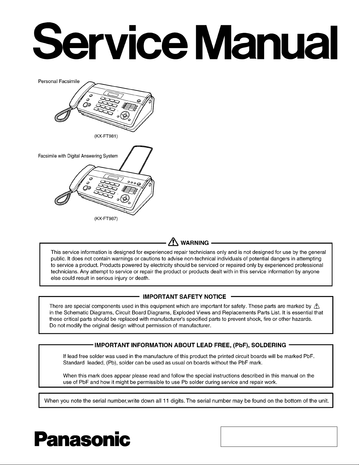
1.2. AC Caution
For safety, before closing the lower cabinet, please make sure of the following precautions.
1. The earth lead is fixed with the screw.
2. The AC lead is connected properly to power supply unit.
3. Wrap the earth lead around the core 3 times.
4. Wrap the AC lead around the core 2 times.
3
Page 4
KX-FT981LA-B / KX-FT987LA-B
1.3. Personal Safety Precautions
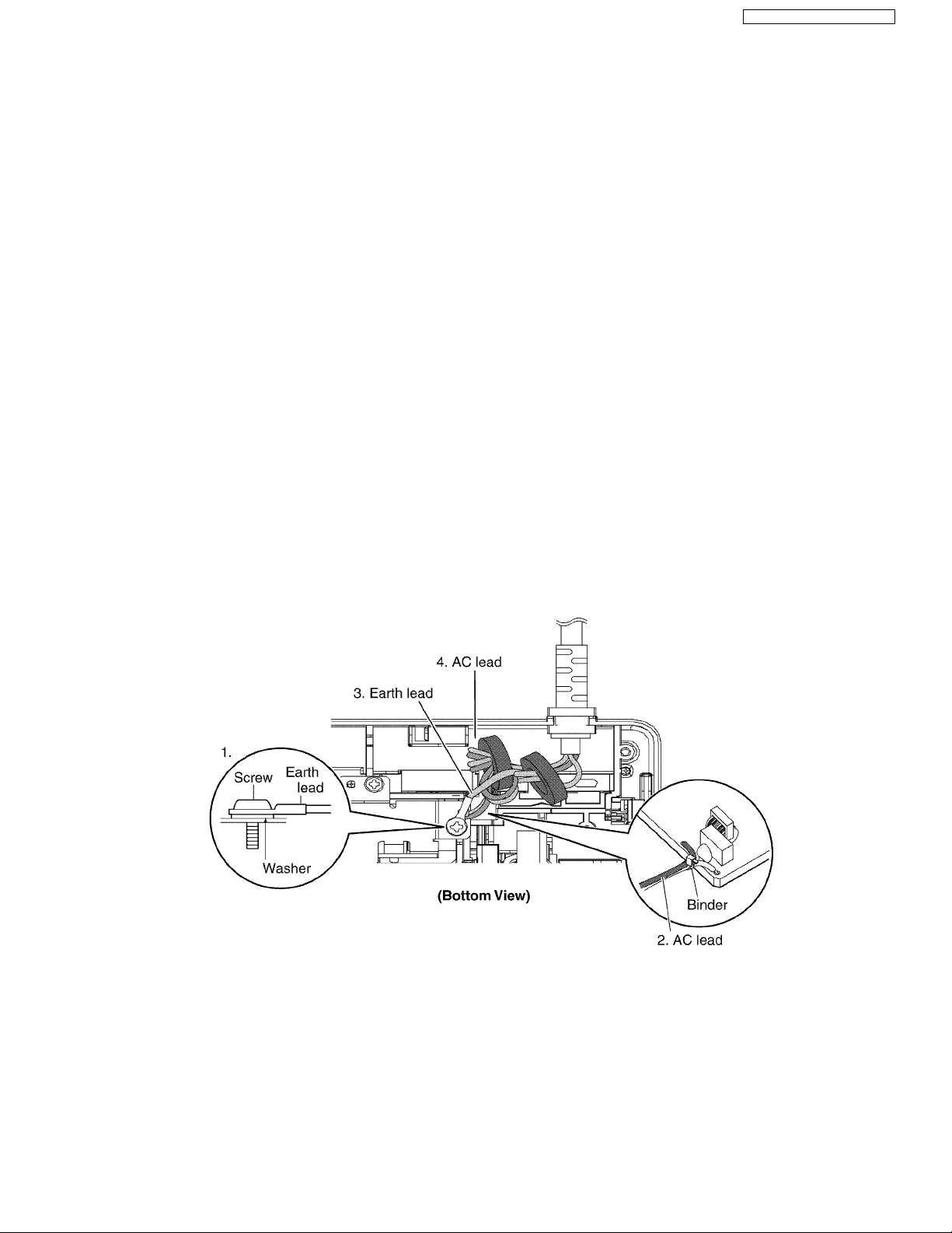
1.3.1. Moving Sections of the Unit
Be careful not to let your hair, clothes, fingers, accessories, etc., become caught in any moving sections of the unit.
The moving sections of the unit are the rollers and a gear. There is a separation roller and a document feed roller which are
rotated by the document feed motor. A gear rotates the two rollers. Be careful not to touch them with your hands, especially
when the unit is operating.
1.3.2. Live Electrical Sections
All the electrical sections of the unit supplied with AC power by the AC power cord are live.
Never disassemble the unit for service with the AC power supply plugged in.
CAUTION:
AC voltage is supplied to the primary side of the power supply unit. Therefore, always unplug the AC power cord before disassembling for service.
4
Page 5
KX-FT981LA-B / KX-FT987LA-B
1.4. Service Precautions
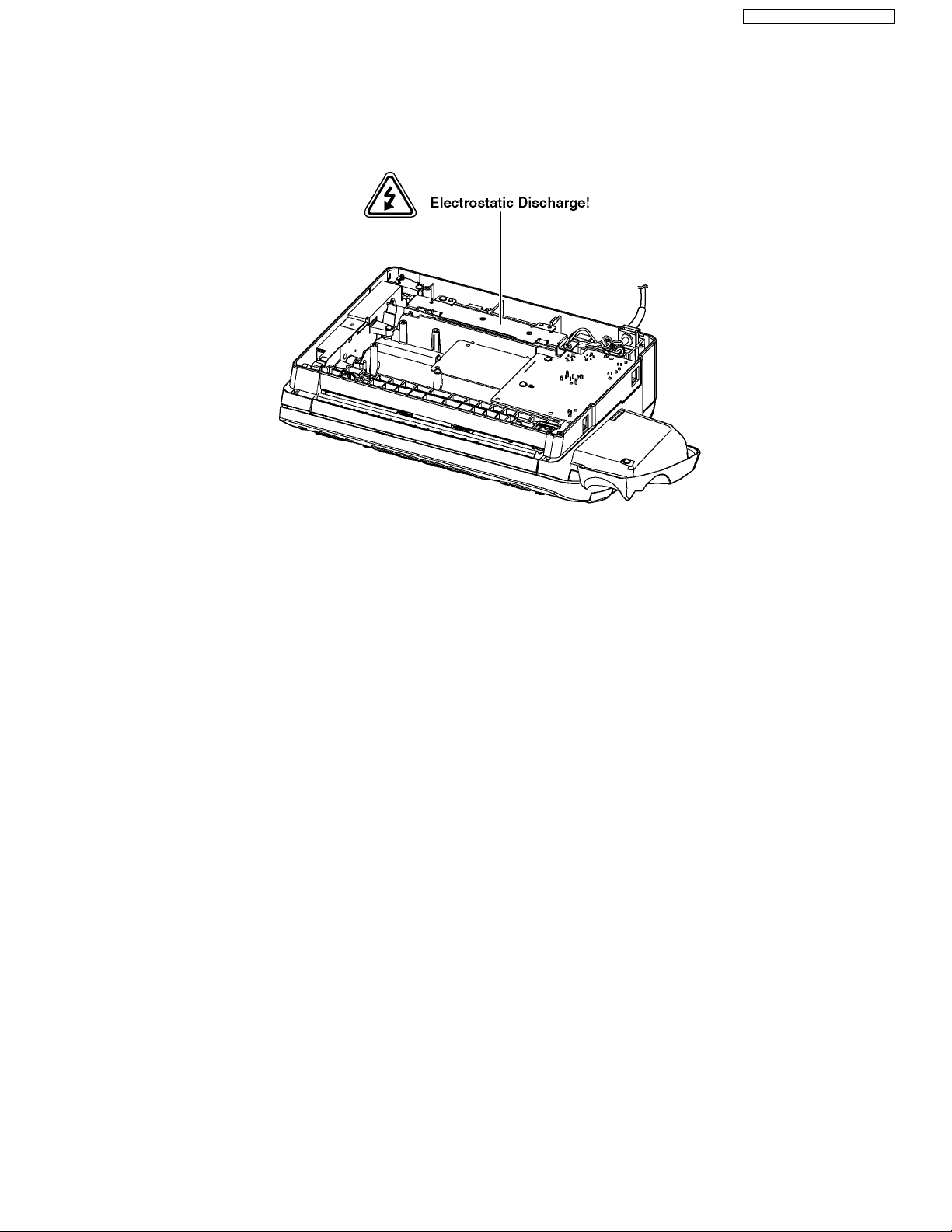
1.4.1. Precautions to Prevent Damage from Static Electricity
Electrical charges accumulate on a person. For instance, clothes rubbing together can damage electric elements or change
their electrical characteristics. In order to prevent static electricity, touch a metallic part that is grounded to release the static
electricity. Never touch the electrical sections such as the power supply unit, etc.
5
Page 6
KX-FT981LA-B / KX-FT987LA-B
2Warning
2.1. About Lead Free Solder (PbF: Pb free)
Note:
In the information below, Pb, the symbol for lead in the periodic table of elements, will refer to standard solder or solder that contains lead.
We will use PbF solder when discussing the lead free solder used in our manufacturing process which is made from Tin, (Sn),
Silver, (Ag), and Copper, (Cu).
This model, and others like it, manufactured using lead free solder will have PbF stamped on the PCB. For service and repair
work we suggest using the same type of solder although, with some precautions, standard Pb solder can also be used.
Caution
PbF solder has a melting point that is 50° ~ 70° F, ( 30° ~ 40°C) higher than Pb solder. Please use a soldering iron with temperature
control and adjust it to 700° ± 20° F, (3 7 0° ± 10°C). In case of using high temperature soldering iron, please be careful not to heat
too long.
PbF solder will tend to splash if it is heated much higher than its melting point, approximately 1100°F, (6 00 °C).
If you must use Pb solder on a PCB manufactured using PbF solder, remove as much of the original PbF solder as possible and be
sure that any remaining is melted prior to applying the Pb solder.
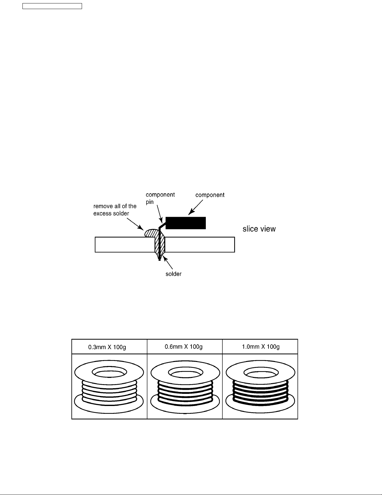
When applying PbF solder to double layered boards, please check the component side for excess which may flow onto the opposite
side (See figure, below).
2.1.1. Suggested PBF Solder
There are several types of PbF solder available commercially. While this product is manufactured using Tin, Silver, and Copper,
(Sn+Ag+Cu), you can also use Tin and Copper, (Sn+Cu), or Tin, Zinc, and Bismuth, (Sn+Zn+Bi). Please check the manufacturer’s specific instructions for the melting points of their products and any precautions for using their product with other
materials.
The following lead free (PbF) solder wire sizes are recommended for service of this product: 0.3mm, 0.6mm and 1.0mm.
6
Page 7
KX-FT981LA-B / KX-FT987LA-B
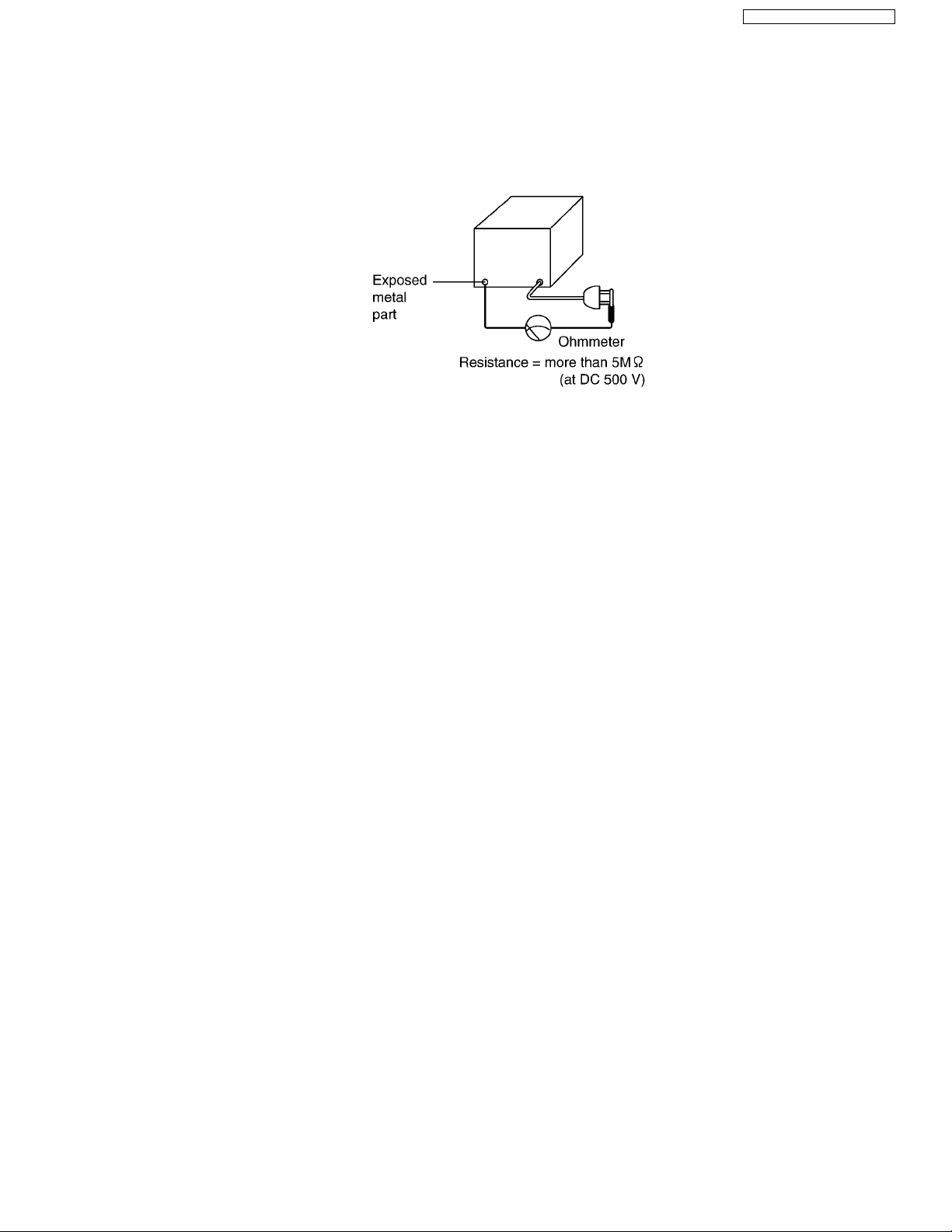
2.2. Insulation Resistance Test
1. Unplug the power cord and short the two prongs of the plug with a jumper wire.
2. Turn on the power switch.
3. Measure the resistance value with an ohmmeter between the jumpered AC plug and each exposed metal cabinet part
(screw heads, control shafts, bottom frame, etc.).
Note: Some exposed parts may be isolated from the chassis by design. These will read infinity.
4. If the measurement is outside the specified limits, there is a possibility of a shock hazard.
2.3. Battery Caution
CAUTION
Danger of explosion if the battery is incorrectly replaced. Replace only with the same or equivalent type recommended by the
manufacturer. Dispose of used batteries according to the manufacturer’s Instructions.
The lithium battery is a critical component (type No. CR2032). Please observe for the proper polarity and the exact location
when replacing it and soldering the replacement lithium battery in.
2.4. Discarding of P. C. Board
When discarding P. C. Board, delete all personal information such as telephone directory and caller list or scrap P. C. Board.
7
Page 8

KX-FT981LA-B / KX-FT987LA-B
3 Specifications
Applicable Lines: Public Switched Telephone Network
Document Size: Max. 216 mm in width
Max. 600 mm in length
Effective Scanning Width: 208 mm
Recording Paper Size: 216 × max. 30 m roll
Effective Printing Width: 208 mm
*1
Transmission Time
: Approx. 15 s/page (Original mode)
Scanning Density: Horizontal: 8 pels/mm
Vertical:
3.85 lines/mm - in standard resolution,
7.7 lines/mm - in fine/photo resolution,
15.4 lines/mm - in super fine resolution
Photo resolution: 64-level
Scanner Type: Contact Image Sensor
Printer Type: Thermal printing
Data Compression System: Modified Huffman (MH), Modified READ (MR)
Modem Speed: 9,600 / 7,200 / 4,800 / 2,400 bps; Automatic Fallback
Operating Environment: 5°C - 35°C, 20% - 80% RH (Relative Humidity)
Dimensions (H×W×D): Approx. height 121 mm × width 352 mm × depth 224 mm
Mass (Weight): KX-FT981: Approx. 2.7 kg
KX-FT987: Approx. 2.8 kg
Power Consumption: Standby: Approx. 1.2 W (KX-FT981)
Standby: Approx. 1.4 W (KX-FT987)
Transmission: Approx. 13 W
Reception: Approx. 30 W (When receiving a 20% black document)
Copy: Approx. 35 W (When copying a 20% black document)
Maximum: Approx. 120 W (When copying a 100% black document)
Power Supply: 120 V AC, 60 Hz
Fax Memory Capacity
*3
:
Approx. 28 pages of memory reception
(Based on the ITU-T No. 1 Test Chart in standard resolution, with original mode.)
Voice Memory Capacity
(KX-FT987 only):
*4
Approx. 12 minutes of recording time including greeting message when no documents are
in memory.
*2
*1
Transmission speed depends upon the contents of the pages, resolution, telephone line conditions and capability of the other
party’s machine.
*2
Transmission speed is based upon the ITU-T No. 1 Test Chart with original mode. If the capability of the other party’s machine is
inferior to your unit, the transmission time may be longer.
*3
If an error occurs during fax reception, such as a paper jam or if the recording paper runs out, the fax and subsequent faxes will
be retained in memory.
*4
Recording time may be reduced by the calling party’s background noise.
Note:
Design and specifications are subject to change without notice.
8
Page 9
KX-FT981LA-B / KX-FT987LA-B
4 General/Introduction
4.1. Optional Accessories
Model No. Item Specifications/Usage
1
KX-A106
*1
Use only the included or specified recording paper. Using other recording paper may affect print quality and/or cause exces-
sive wear to the thermal head.
Standard thermal recording paper*
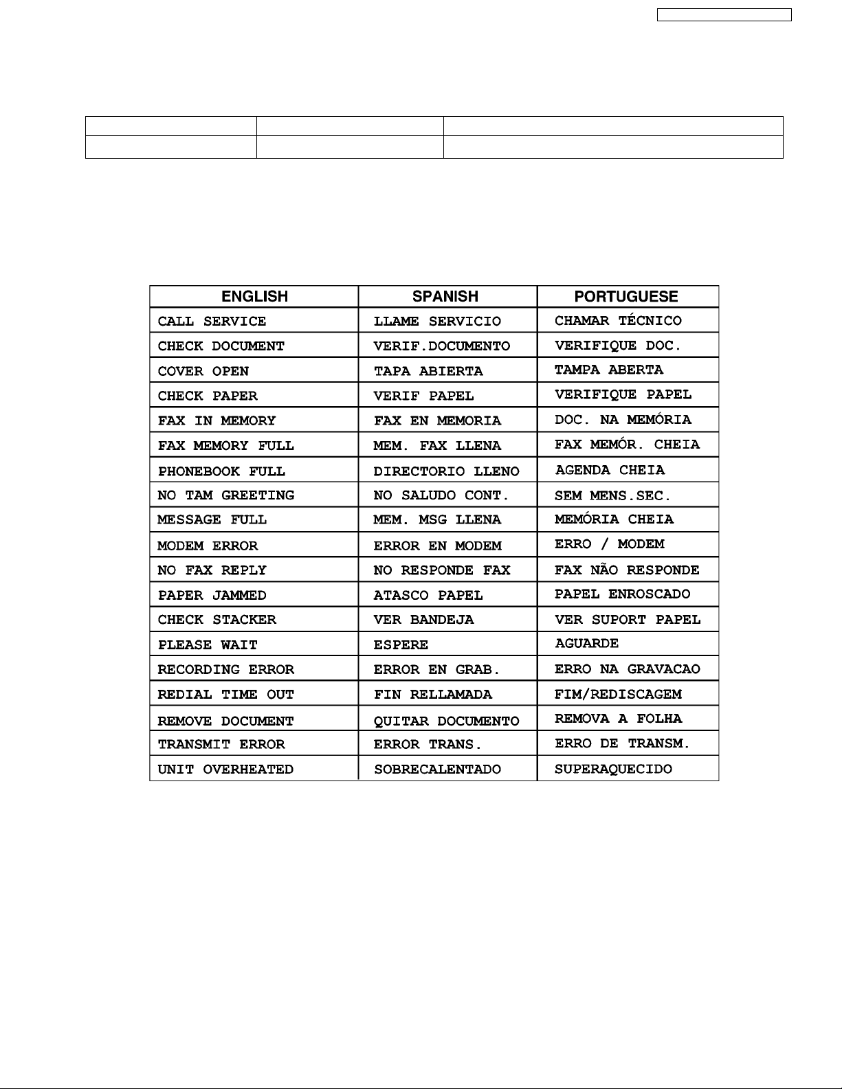
4.2. Translation Lists
4.2.1. Error Messages-Display
216 mm × 30 m roll, with 25 mm core
9
Page 10
KX-FT981LA-B / KX-FT987LA-B
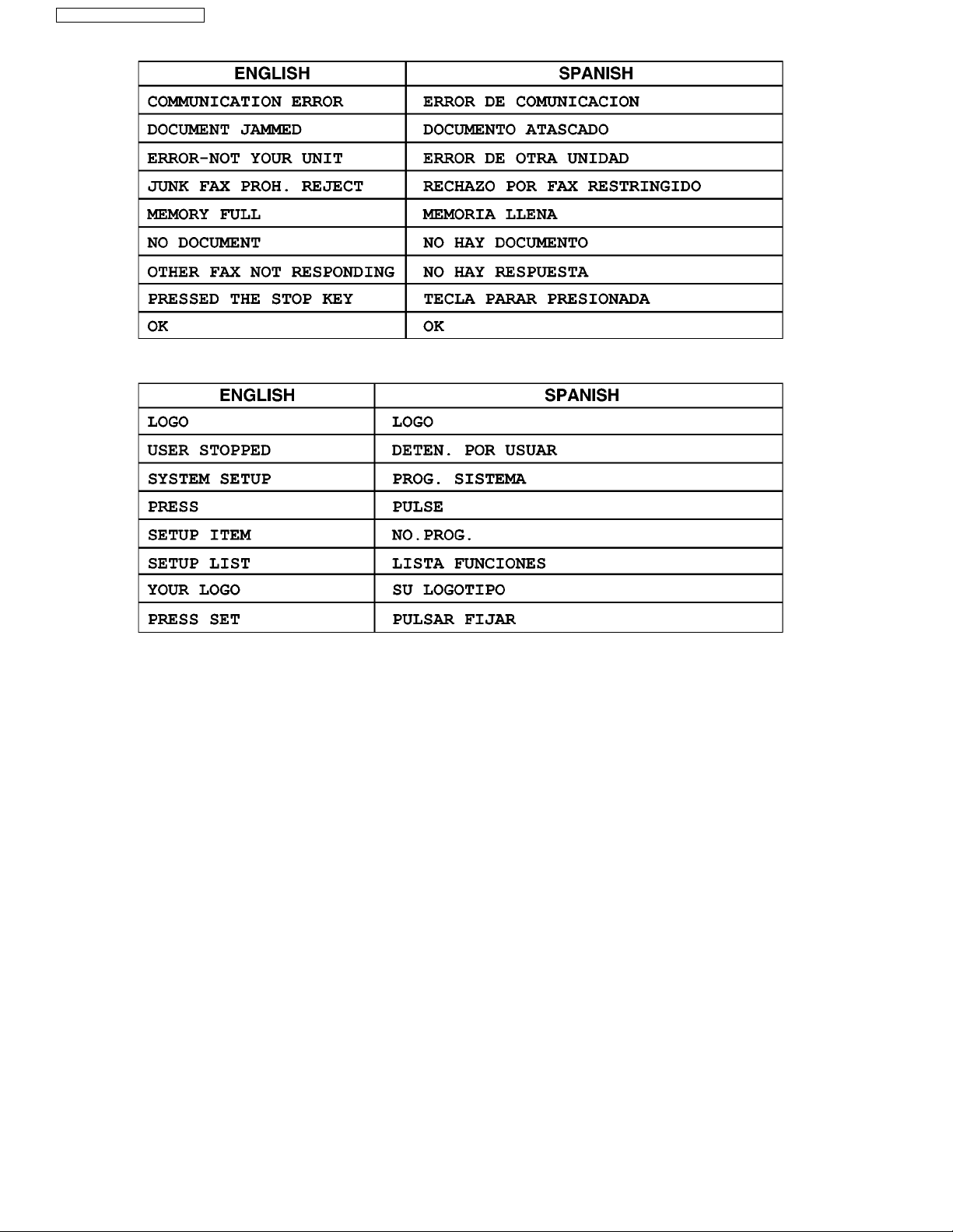
4.2.2. Error Messages-Report
4.2.3. Other-Display
5Features
General
• LCD (Liquid Crystal Display) readout
• The display and reports will be in the selected language.
(Spanish / Portuguese / English)
• Automatic Paper Cutter (KX-FT987 only)
Facsimile
• Document memory
• Automatic document feeder (10 sheets)
• 64-Level halftone resolution
Standard/Fine/Photo/Super Fine
• Broadcast
Integrated Telephone System
• Phonebook function (100 names)
• One-Touch Dial (10 stations)
• Caller ID compatible
• Monitor (KX-FT981 only)
• Digital SP-Phone (KX-FT987 only)
Digital Answering System (KX-FT987 only)
• Voice Time/Day Stamp
• 12-Minutes recording time
10
Page 11
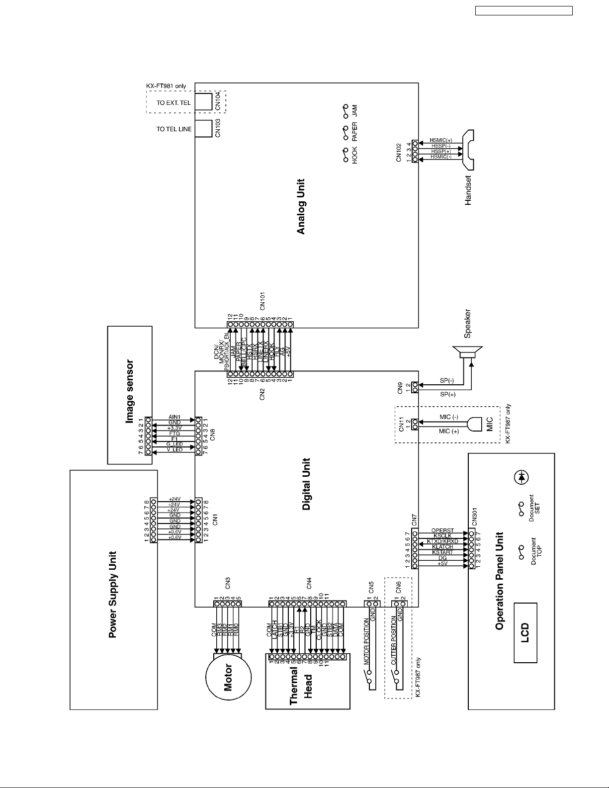
6 Technical Descriptions
6.1. Connection Diagram
KX-FT981LA-B / KX-FT987LA-B
11
Page 12

KX-FT981LA-B / KX-FT987LA-B
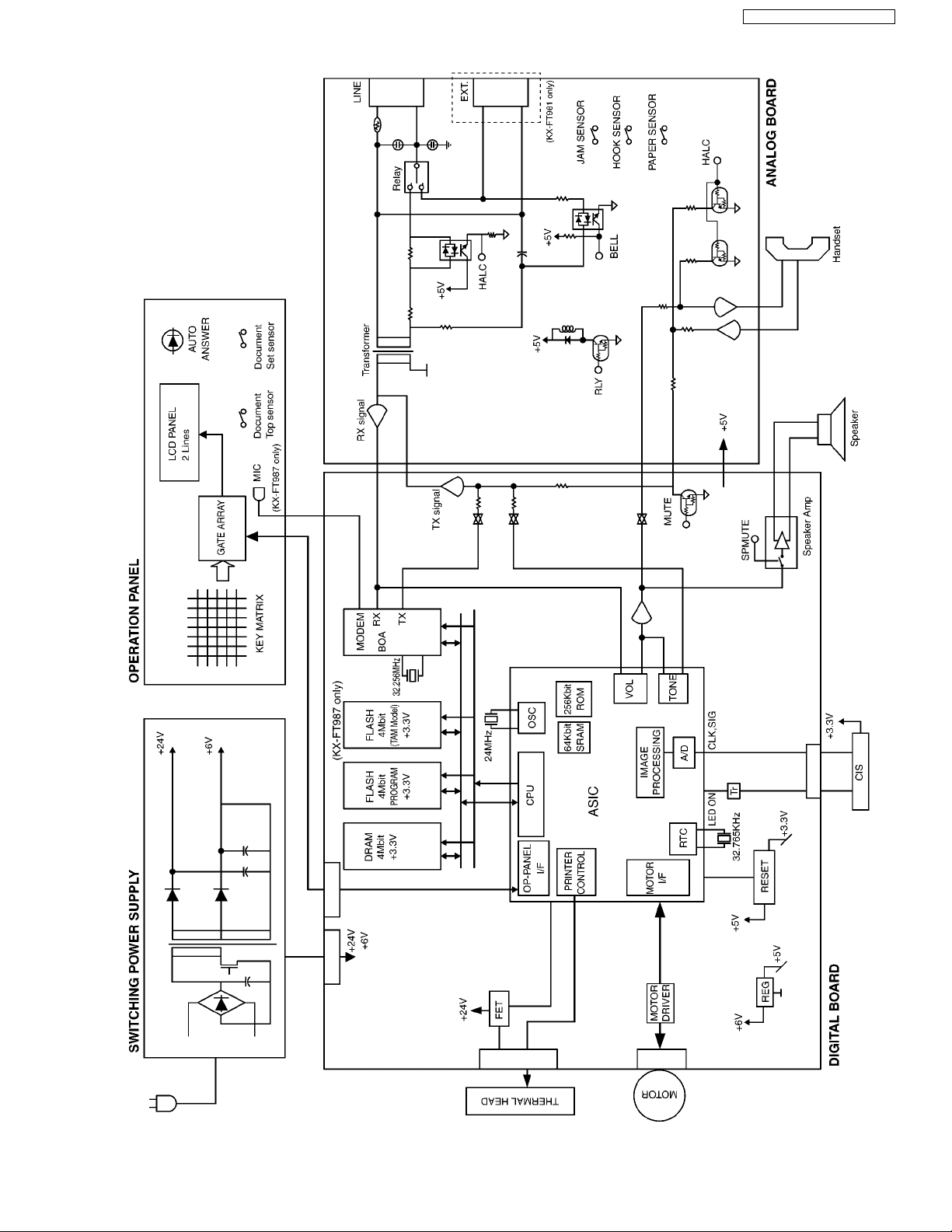
6.2. General Block
The following is an outline of each device IC on the digital board. (Refer to General Block Diagram (P.13).).
1. ASIC (IC1)
Composed mainly of an address decoder and a modem control.
Controls the general FAX operations.
Controls the operation panel I/F.
Controls the thermal head I/F and CIS I/F.
Performs the image processing.
CPU and Real time clock
Provides the reset pulse for each of the major ICs.
2. Flash ROM (IC2)
Contains all of the program instructions on the unit operations.
This memory is used mainly for the parameter working in the storage area.
3. Dynamic RAM (IC4)
This memory is used mainly for the parameter working in the storage area.
4. MODEM (IC5)
Performs the modulation and the demodulation for FAX communication.
5. Read Section
CIS image sensor to read transmitted documents.
6. Motor Driver (IC7)
Drives the transmission motor and the reception motor.
7. Thermal Head
Contains heat-emitting elements for dot matrix image printing.
8. Sensor Section
Composed of a cover open, a document set switch, a document top switch, a paper sensor switch, a jam sensor switch, and
a hook sensor switch.
9. Power Supply Board Switching Section
Supplies +6V and +24V to the unit.
10. Flash MEMORY (IC6) (KX-FT987 only)
Voice Prompt (TAM) D/L (DownLoad) area.
12
Page 13
6.2.1. General Block Diagram
KX-FT981LA-B / KX-FT987LA-B
13
Page 14

KX-FT981LA-B / KX-FT987LA-B
6.3. Control Section
6.3.1. ASIC (IC1)
This custom IC is used for the general FAX operations.
1. CPU:
This model uses a Z80 equivalent to the CPU operating
at 24 MHz. Most of the peripheral functions are performed
by custom-designed LSIs. Therefore, the CPU only works
for processing the results.
2. RTC:
Real Time Clock
3. DECODER:
Decodes the address.
4. ROM/RAM I/F:
Controls the SELECT signal of ROM or RAM and the
bank switching.
5. CIS I/F:
Controls the document reading.
Note:
This memory is incorporated into the ASIC (IC1) and used for the image processing.
6. IMAGE DATA RAM:
This memory is programmed into the ASIC and uses 8
KB for the image processing.
7. THERMAL HEAD I/F:
Transmits the recorded data to the thermal head.
8. MOTOR I/F:
Controls the transmission motor which feeds the document.
Controls the receiving motor which feeds the recording
paper.
9. OPERATION PANEL I/F:
Serial interface with Operation Panel.
10. I/O PORT:
I/O Port Interface.
11. ANALOG UNIT:
Electronic volume for the monitor.
Sends beep tones, etc.
Descriptions of Pin Distribution (IC1)
NO. SIGNAL I/O POWER SUPPLIED
1 VSSA1 GND POWER SOURCE (ANALOG GND)
2 VDDA 3.3 3.3V POWER SOURCE (ANALOG +3.3V)
3 AIN1 A 3.3V CIS IMAGE SIGNAL INPUT (ATN1)
4 AIN2 A 3.3V THERMISTOR TEMPERATURE WATCH INPUT
5 AIN3 A 3.3V LINE VOLTAGE DETECTION SIGNAL INPUT (DCIN)
6 AMON A 3.3V ANALOG SIGNAL MONITOR TERMINAL
7 VSS1 GND POWER SOURCE (GND)
8 X32OUT O 3.3V/BATT RTC (32.768KHz) CONNECTION
9 X32IN I 3.3V/BATT RTC (32.768KHz) CONNECTION
10 VDD (3.3V / B) ----- POWER SOURCE (+3.3V/LITHIUM BATTERY)
11 XBACKEN I 3.3V/BATT BACKUP ENABLE
12 XRAMCS O 3.3V/BATT XRAMCS
13 VDD (3.3V / B) ----- POWER SOURCE(+3.3V / LITHIUM BATTERY)
14 VDD (2.5V/B) ----- POWER SOURCE (+2.5V / LITHIUM BATTERY)
15 FTG O 3.3V SH SIGNAL OUTPUT FOR CIS (FTG)
16 F1 O 3.3V 01 SIGNAL OUTPUT FOR CIS (F1)
17 F2/OP O 3.3V OUTPUT PORT (HEADON)
18 FR/OP O 3.3V OUTPUT PORT (MDMRST)
19 CPC I 3.3V INPUT PORT (BELL/CPC)
20 RVN I 3.3V INPUT PORT (PAPER)
21 IRDATXD I 3.3V INPUT PORT (JAM)
22 IRDARXD O 3.3V OUTPUT PORT (HSTX MUTE)
23 TXD/IOP I 3.3V TXD
24 RXD/IOP I/O 3.3V RXD
25 RTS/IOP I 3.3V RTS
26 CTS/IOP I/O 3.3V CTS
27 VDD (2.5V)1 ----- POWER SOURCE (+2.5V)
28 TONE1 A 3.3V TONE OUTPUT
29 TONE2 A 3.3V TONE OUTPUT
30 VOLUREF/VOLU1 A 3.3V ANALOG REF VOLTAGE
31 VOLUOUT/VOLU2 A 3.3V VOLUME OUTPUT
32 VOLUIN/VOLU3 A 3.3V VOLUME INPUT
33 XNMI I 3.3V HIGH FIXED
34 FMEMDO/IOP O 3.3V OUTPUT PORT (LED ON)
35 VDD (3.3V)1 ----- POWER SOURCE (+3.3V)
36 VSS2 GND POWER SOURCE (GND)
37 VSS3 GND POWER SOURCE (GND)
DESCRIPTION
VOLTAGE
14
Page 15

KX-FT981LA-B / KX-FT987LA-B
NO. SIGNAL I/O POWER SUPPLIED
DESCRIPTION
VOLTAGE
38 VDD (3.3V)2 ----- POWER SOURCE (+3.3V)
39 MIDAT/IOP I/O 3.3V PORT (TONE1EN)
40 MICLK/IOP O 3.3V OUTPUT PORT (MDMTXEN)
41 MILAT/IOP I/O 3.3V PORT (HSRXEN)
42 20KOSC/IOP O 3.3V OUTPUT PORT (PSHORT/ACK_EN)
43 XWAIT I 3.3V INPUT PORT (HOOK)
44 XHSTRD/IOP I 3.3V INPUT PORT (TEST)
45 XHSTWR/IOP O 3.3V OUTPUT PORT (DCN)
46 XOPRBE O 3.3V OUTPUT PORT (MFCS)
47 ADR15 O 3.3V CPU ADDRESS BUS 15 (NOT USED)
48 ADR14 O 3.3V CPU ADDRESS BUS 14 (NOT USED)
49 ADR13 O 3.3V CPU ADDRESS BUS 13 (NOT USED)
50 VDD (2.5V)2 ----- POWER SOURCE (+2.5V)
51 XOUT O 3.3V SYSTEM CLOCK (24MHz)
52 XIN I 3.3V SYSTEM CLOCK (24MHz)
53 VSS4 GND POWER SOURCE (GND)
54 VDD (3.3V)3 ----- POWER SOURCE (+3.3V)
55 XTEST O 3.3V 24MHz CLOCK
56 TEST1 I 3.3V HIGH FIXED
57 TEST2 I 3.3V HIGH FIXED
58 TEST3 I 3.3V HIGH FIXED
59 TEST4 I 3.3V HIGH FIXED
60 XMDMINT I 3.3V MODEM INTERRUPT
61 XMDMCS O 3.3V MODEM CHIP SELECT
62 XRAS/IOP O 3.3V DRAM ROW ADDRESS STROBE (RAS)
63 XCAS1/IOP O 3.3V DRAM COLUMN ADDRESS STROBE (CAS)
64 XCAS2/IOP I 3.3V PORT (SPMUTE)
65 XRESCS2 O 3.3V FLASH CHIP SELECT (XRESCS2)
66 DB3 I/O 3.3V CPU DATA BUS 3
67 DB2 I/O 3.3V CPU DATA BUS 2
68 DB4 I/O 3.3V CPU DATA BUS 4
69 DB1 I/O 3.3V CPU DATA BUS 1
70 DB5 I/O 3.3V CPU DATA BUS 5
71 VDD (3.3V)4 ----- POWER SOURCE (+3.3V)
72 VSS5 GND POWER SOURCE (GND)
73 VSS6 GND POWER SOURCE (GND)
74 VDD (3.3V)5 ----- POWER SOURCE (+3.3V)
75 DB0 I/O 3.3V CPU DATA BUS 0
76 DB6 I/O 3.3V CPU DATA BUS 6
77 DB7 I/O 3.3V CPU DATA BUS 7
78 XROMCS O 3.3V FLASH (IC2) CHIP SELECT
79 XRD O 3.3V CPU RD
80 XWR O 3.3V CPU WR
81 ADR0 O 3.3V CPU ADDRESS BUS 0
82 ADR1 O 3.3V CPU ADDRESS BUS 1
83 ADR2 O 3.3V CPU ADDRESS BUS 2
84 ADR3 O 3.3V CPU ADDRESS BUS 3
85 ADR4 O 3.3V CPU ADDRESS BUS 4
86 ADR5 O 3.3V CPU ADDRESS BUS 5
87 VSS7 GND POWER SOURCE (GND)
88 VDD (2.5V)3 ----- POWER SOURCE (+2.5V)
89 ADR6 O 3.3V CPU ADDRESS BUS 6
90 ADR7 O 3.3V CPU ADDRESS BUS 7
91 ADR8 O 3.3V CPU ADDRESS BUS 8
92 ADR9 O 3.3V CPU ADDRESS 9
93 ADR10 O 3.3V CPU ADDRESS 10
94 ADR11 O 3.3V CPU ADDRESS 11
95 ADR12 O 3.3V CPU ADDRESS 12
96 RBA0 O 3.3V ROM/RAM BANK ADDRESS 0
97 RBA1 O 3.3V ROM/RAM BANK ADDRESS 1
98 RBA2 O 3.3V ROM/RAM BANK ADDRESS 2
99 RBA3 O 3.3V ROM/RAM BANK ADDRESS 3
100 RBA4 O 3.3V ROM/RAM BANK ADDRESS 4
101 RBA5 O 3.3V ROM/RAM BANK ADDRESS 5
102 RBA6/IOP O 3.3V OUTPUT PORT (NC)
103 STB1 O 3.3V STROBE SIGNAL OUTPUT TO THERMAL HEAD
15
Page 16
KX-FT981LA-B / KX-FT987LA-B
NO. SIGNAL I/O POWER SUPPLIED
VOLTAGE
104 STB2 O 3.3V STROBE SIGNAL OUTPUT TO THERMAL HEAD
105 STB3 O 3.3V OUTPUT PORT (NC)
106 XRESET I 3.3V RESET INPUT
107 VDD (3.3V)6 ----- POWER SOURCE (+3.3V)
108 VSS8 GND POWER SOURCE (GND)
109 VSS9 GND POWER SOURCE (GND)
110 VDD (3.3V)7 ----- POWER SOURCE (+3.3V)
111 XORESET O 3.3V NOT USED
112 VDD(5V) ----- POWER SOURCE (+5V)
113 VSS10 GND POWER SOURCE (GND)
114 XRESETI I 3.3V RESET INPUT
115 XWDERR O 3.3V WATCHED ERROR OUTPUT SIGNAL
116 THDAT O 3.3V RECORDED IMAGE OUTPUT (THDAT)
117 THCLK O 3.3V CLOCK OUTPUT FOR DATA TRANSFER (THCLK)
118 THLAT O 3.3V PULSE OUTPUT FOR DATA LATCH (THLAT)
119 STBNP I 3.3V INPUT PORT (MOT-POS)
120 RM0/IOP O 3.3V MOTOR A PHASE
121 RM1/IOP O 3.3V MOTOR B PHASE
122 RM2/IOP O 3.3V MOTOR /A PHASE
123 RM3/IOP O 3.3V MOTOR /B PHASE
124 RXE/IOP O 3.3V MOTOR ENABLE
125 TMO O 3.3V OUTPUT PORT (R1)
126 VDD (2.5V)4 ----- POWER SOURCE (+2.5V)
127 VSS11 GND POWER SOURCE (GND)
128 TM1/IOP O 3.3V OUTPUT PORT (R2)
129 TM2/IOP O 3.3V OUTPUT PORT (CISON)
130 TM3/IOP O 3.3V OUTPUT PORT (RLY)
131 TXE/IOP I 3.3V INPUT PORT (CUT_POS)
132 KSTART O 3.3V OPERATION PANEL CONTROL
133 KLATCH O 3.3V OPERATION PANEL CONTROL
134 KSCLK O 3.3V OPERATION PANEL CONTROL
135 KTXD O 3.3V OPERATION PANEL CONTROL
136 KRXD I 3.3V OPERATION PANEL CONTROL
137 FMEMCLK/IOP O 3.3V OUTPUT PORT (OPRESET)
138 FMEMDI/IOP O 3.3V OUTPUT PORT (NC)
139 ADSEL1 O 3.3V CHANNEL SELECT SIGNAL FOR AIN2
140 VDDA (2.5V) 2.5V POWER SOURCE (ANALOG +2.5V)
141 VREFB A 3.3V A/D CONVERTER'S ZERO STANDARD VOLTAGE
OUTPUT
142 VCL A 3.3V ANALOG PART STANDARD VOLTAGE SIGNAL
143 VREFT A 3.3V A/D CONVERTER'S FULL SCALE VOLTAGE OUTPUT
144 VSSA2 GND POWER SOURCE (ANALOG GND)
DESCRIPTION
Connection to operation reset circuit
16
Page 17
KX-FT981LA-B / KX-FT987LA-B
6.3.2. Flash Memory (IC2)
This 512KB ROM (FLASH MEMORY) carries a common area of 32KB and bank areas which each have 8KB (BK4~BK63). The
addresses from 0000H to 7FFFH are for the common area and from 8000H to 9FFFH are for the bank areas.
6.3.3. Dynamic RAM (IC4)
The DRAM serves as CPU and receives memory.
The address is F200H~F3FFH (DRAM access window 1) and F600H~F7FFH (DRAM access window 2).
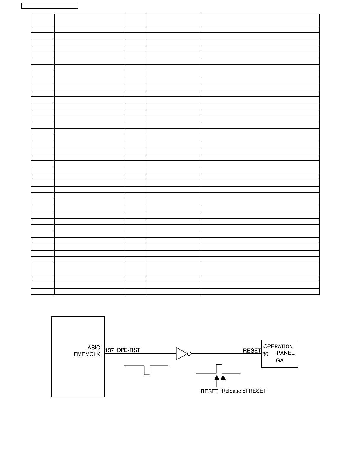
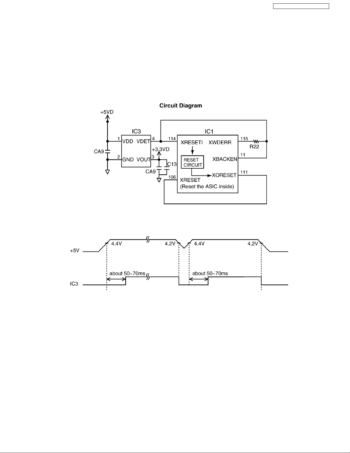
6.3.4. Reset Circuit (Watch dog timer)
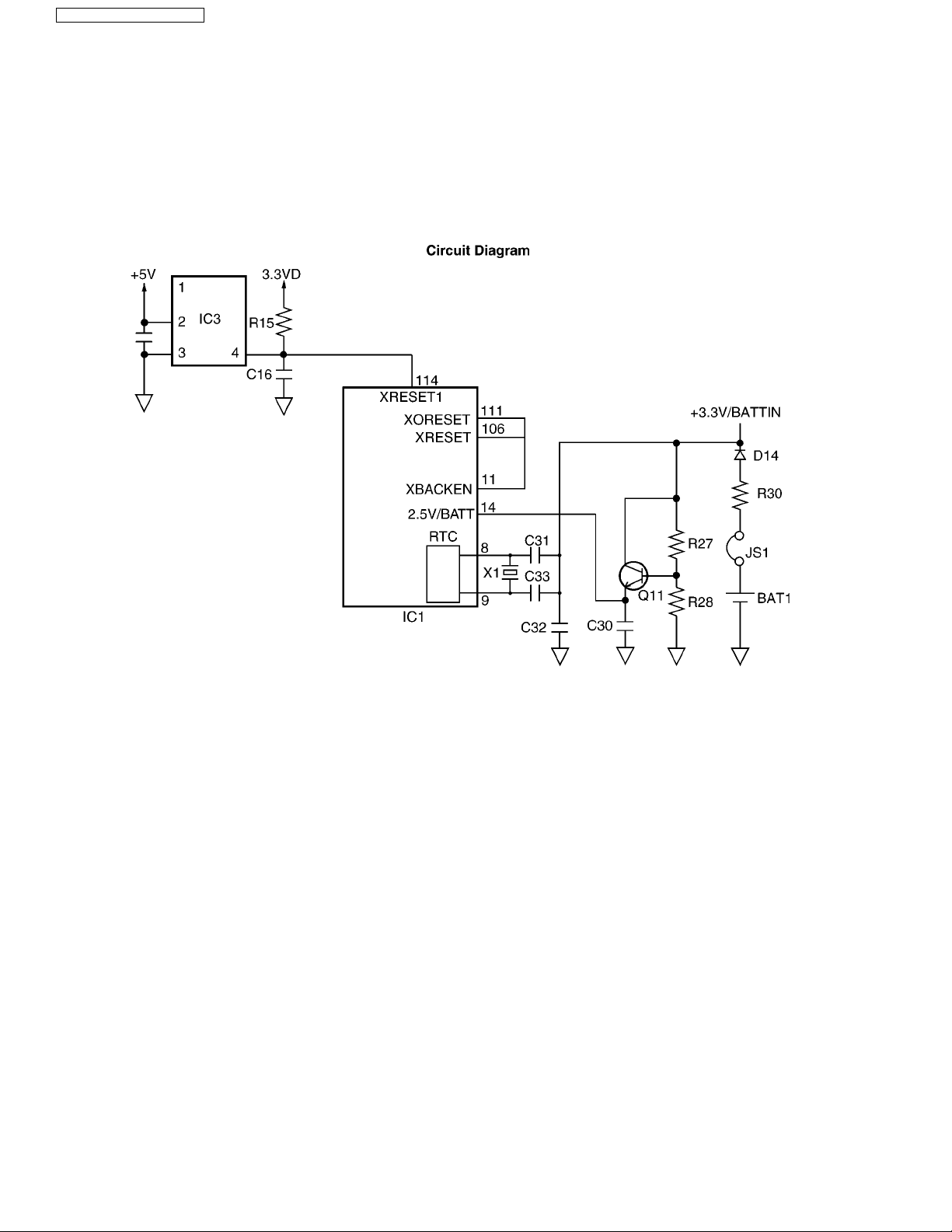
The output signal (reset) from pin 4 of the voltage detect IC (IC3) is input to the ASIC (IC1) 114 pin.
1. During a momentary power interruption, a positive reset pulse of 50~70 msec is generated and the system is reset completely.
2. The watch dog timer, built-in the ASIC (IC1), is initialized by the CPU about every 1.5 ms.
When a watch dog error occurs, pin 115 of the ASIC (IC1) becomes low level.
The terminal of the 'WDERR' signal is connected to the reset line, so the 'WDERR' signal works as the reset signal.
17
Page 18
KX-FT981LA-B / KX-FT987LA-B
6.3.5. RTC Back up Circuit
1. Function
This unit has a lithium battery (BAT1) which works for the Real Time Clock (RTC, Integrated into ASIC:IC1).
The RTC continues functioning, even when the power switch is OFF, backed up by a lithium battery.
2. Circuit Operation
When the power is turned ON, power is supplied to RTC (IC1).
At this time, the voltage at pin 14 of RTC (IC1) is +3.3V. When the power is turned OFF, the battery supplies the power to RTC
through JS1, R30, D14. At that time, the voltage at pin 14 of IC1 are about +2.5V. When the power is OFF and the +5V and
+3.3V voltages decrease, the LOW is input to pin 114 of IC1. Pin 111 of IC1 outputs the reset signals. Pin 11 of IC1 become
low, then RTC (IC1) go into the back up mode, when the power consumption is lower.
18
Page 19
KX-FT981LA-B / KX-FT987LA-B
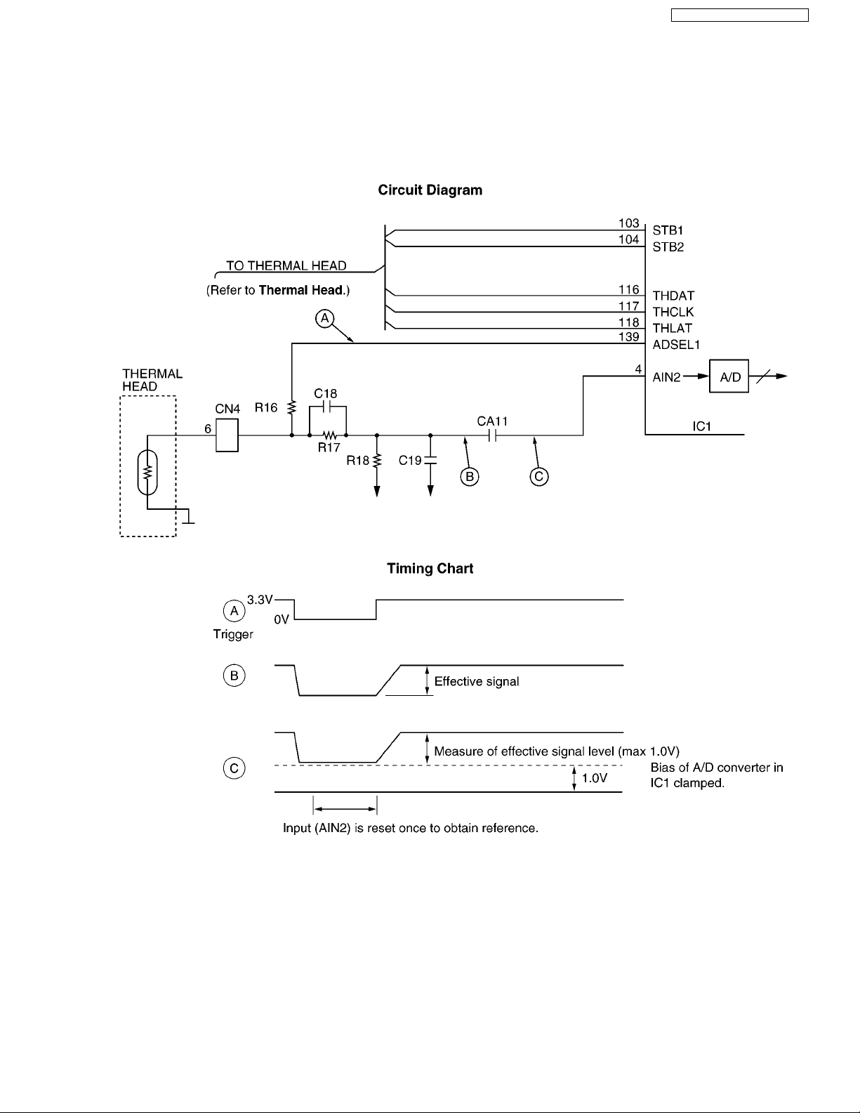
6.3.6. Supervision Circuit for the Thermal Head Temperature
1. Function
The thermistor changes the resistor according to the temperature and uses the thermistor's characteristics. The output of pin
139 of IC1 becomes a low level. Then when it becomes a high level, it triggers point A. In point C, according to the voltage
output time, the thermal head's temperature is detected.
After the thermal head temperature is converted to voltage in B, it is then changed to digital data in the A/D converter inside
IC1. The CPU decides the strobe width of the thermal head according to this value. Therefore, this circuit can keep the thermal head at an even temperature in order to stabilize the printing density and prevent the head from being overheated.
REFERENCE:
Thermal Head (P.22)
19
Page 20

KX-FT981LA-B / KX-FT987LA-B
6.4. Facsimile Section
6.4.1. Image Data Flow During Facsimile Operation
Copy (Fine, Super-Fine, Photo)
1. Line information is read by CIS (to be used as the reference white level) via route (1), and is input to IC1. Refer to Block Diagram (P.21)
2. In IC1, the data is adjusted to a suitable level for A/D conversion in the Analog Signal Processing Section, and via route (2) it
is input to A/D conversion (8 bit). After finishing A/D conversion, the data is input to the Image Processing Section via route
(3). Then via route (4) and route (5), it is stored in RAM as shading data.
3. The draft’s information that is read by CIS is input to IC1 via route (1). After it is adjusted to a suitable level for A/D conversion
via route (2), the draft’s information is converted to A/D (8 bit), and it is input to the Image Processing Section. The other side,
the shading data which flows from RAM via route (6) and route (7), is input to the Image Processing Section. After finishing
the draft’s information image processing, white is regarded as "0" and black is regarded as "1". Then via routes (4) and (5),
they are stored in RAM.
4. The white/black data stored as above via routes (6) and (8) is input to the P/S converter. The white/black data converted to
serial data in the P/S converter is input to the Thermal Head via route (9) and is printed out on recording paper.
Note:
Fine: Reads 3.85 lines/mm
Super Fine: Reads 7.7 lines/mm
Photo: Reads 15.4 lines/mm
Transmission
1. Same processing as Copy items 1 - 3.
2. The data stored in the RAM of IC1 is output from IC1 via routes (6) and (10), and is stored in the system bus.
Via route (11), it is stored in the communication buffer inside DRAM (IC4).
3. While retrieving data stored in the communication buffer synchronous with the modem, the CPU (inside IC1) inputs the data to
the modem along route (12), where it is converted to serial analogue data and forwarded over the telephone lines via the
NCU Section.
Reception
1. The serial analog image data is received over the telephone lines and input to the modem via the NCU section, where it is
demodulated to parallel digital data. Then the CPU (IC1) stores the data in the communication buffer DRAM (IC4) along route
(11).
2. The data stored in DRAM (IC4) is decoded by the CPU (IC1) via route (12), and is stored in RAM via routes (13) and (5).
3. Same processing as Copy item 4.
20
Page 21
6.4.2. Block Diagram
KX-FT981LA-B / KX-FT987LA-B
21
Page 22
KX-FT981LA-B / KX-FT987LA-B
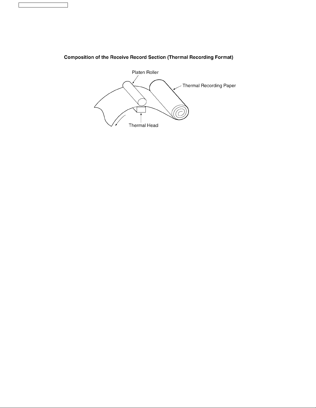
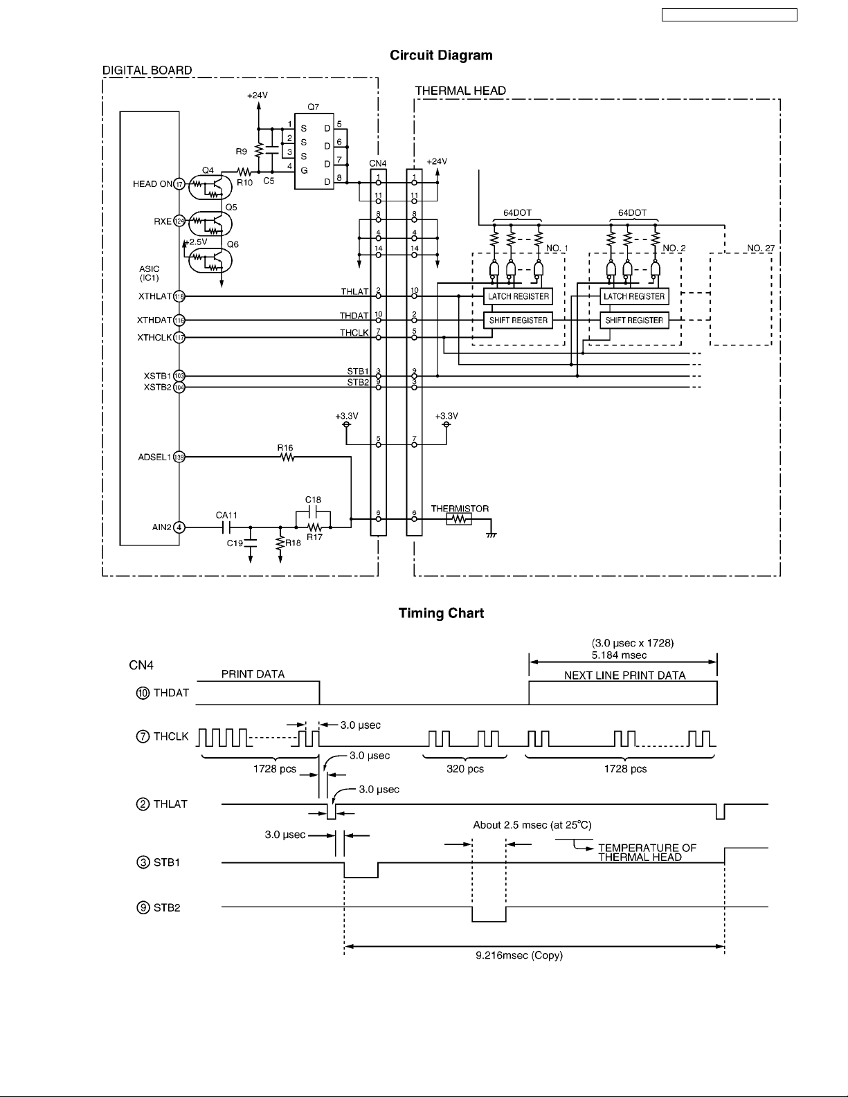
6.4.3. Thermal Head
1. Function
This unit utilizes state of the art thermal printer technology.
The recording paper (roll paper) is chemically processed. When the thermal head contacts this paper it emits heat momentarily, and black dots (appearing like points) are printed on the paper. If this continues, letters and/or diagrams appear, and the
original document is reproduced.
2. Circuit Operation
There are 27 driver ICs aligned horizontally on the thermal head and each one of these ICs can drive 64 heat emitting registers. This means that one line is at a density of 64×27=1728 dots=(8 dots/mm).
White/Black (white=0, black=1) data in one line increments is synchronized at IC1 pin 117 (THCLK), and sent from IC1 pin 116
(THDAT) to the shift register of the ICs. The shift registers of the 27 ICs are connected in series, and upon the shift of dot
increment 1728, all the shift registers become filled with data, and a latch pulse is emitted to each IC from IC1 pin 118
(THLAT).With this latch pulse, all the contents of the shift registers are latched to the latch registers. Thereafter, through the
addition of strobes from the IC1 pins (103 - 104) only black dot locations (=1) among latched data activates the driver, and the
current passes to heat the emitting body causing heat emission.
Here, the two line strobes, STB1 and STB2, impress at intervals of 9.216 msec, as required for one-line printout.
The sequence is shown on the next page. [Moreover, for the strobe width, the thermistor value inside the thermal head is
detected according to IC1 pin 4. Depending on that value, the strobe width is recorded in FLASH (IC2).
Accordingly, the strobe width is determined.
When the thermal head is not used, the IC1 (17, HEADON) becomes low, Q6 turns OFF, Q7 turns OFF, and the +24 V power
supply for the thermal head driver is not impressed to protect the IC.
22
Page 23
KX-FT981LA-B / KX-FT987LA-B
23
Page 24
KX-FT981LA-B / KX-FT987LA-B
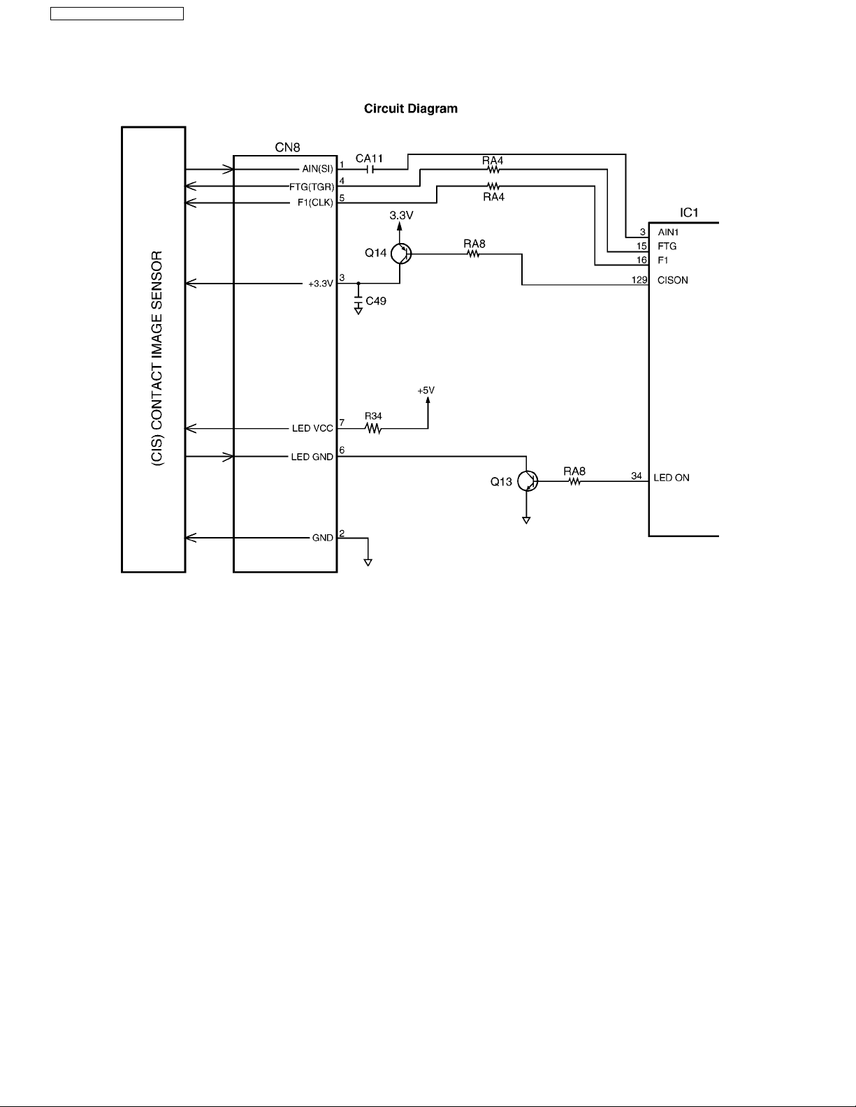
6.4.4. Scanning Block
The scanning block of this device consists of a control circuit and a contact image sensor made up of a celfoc lens array, a light
source, and photoelectric conversion elements.
When an original document is inserted and the start button pressed, pin 129 of IC1 goes to a low level and the transistor Q14 turns
on.This applies voltage to the light source to light it. The contact image sensor is driven by each of the FTG-F1 signals output from
IC1, and the original image illuminated by the light source undergoes photoelectric conversion to output an analogue image signal
(AIN). The analogue image signal is input to the system ASIC on AIN1 (pin 3 of IC1) and converted into 8-bit data by the A/D converter inside IC1. Then this signal undergoes digital processing in order to obtain a high-quality image.
24
Page 25
KX-FT981LA-B / KX-FT987LA-B
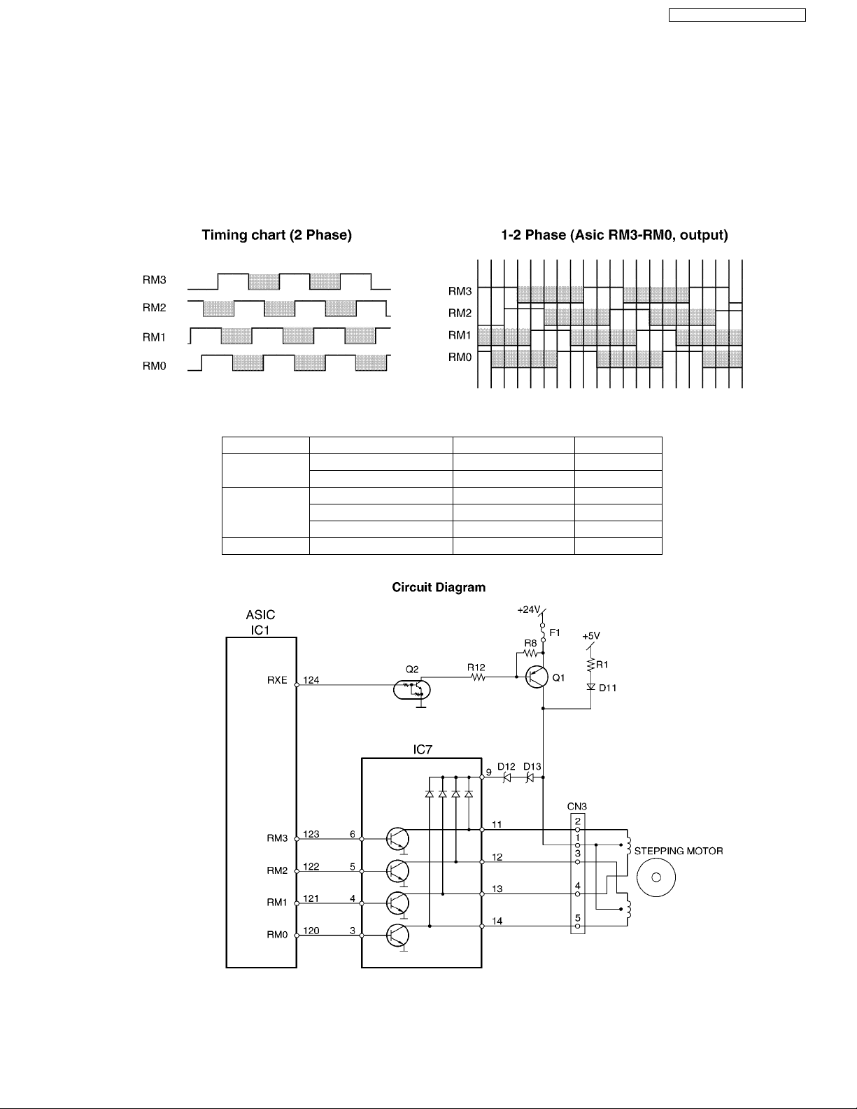
6.4.5. Stepping Motor Drive Circuit
1. Function
One individual stepping motor is used for transmission and reception. It feeds the document or recording paper synchronized
for reading or printing.
2. Circuit Operation
During motor drive, ASIC IC1 pin 124 becomes a high level, and Q2 and Q1 go ON as a result. +24 V is supplied tothe motor
coil.
Stepping pulses are output from ASIC IC1, causing driver IC7 to go ON. The motor coil is energized sequentially in 2 phase
increments or 1-2 phase increments, which causes a 1-step rotation. A 1-step rotation is 0.13mm of recording paper or document paper. The timing chart is below.
Stepping Motor Phase Pattern
Function Mode Phase Pattern Speed
Copy Fine/Photo 1-2 432 pps
Super Fine 1-2 216 pps
FAX STD 2 432 pps
Fine/Photo 1-2 432 pps
Super Fine 1-2 216 pps
——— Paper Feed 2 432 pps
When the motor is OFF, ASIC IC1 pin 124 becomes a low level and Q2 and Q1 also turns OFF. Instead of +24V, +5V is supplied
through D11 so that the motor is held in place.
25
Page 26
KX-FT981LA-B / KX-FT987LA-B
6.5. Sensors and Switches
All of the sensors and switches are shown below.
Sensor Circuit
Location
DIGITAL CN5 Motor Position Sensor [CALL SERVICE]
ANALOG SW101 Cover Open / Paper Sensor [COVER OPEN] and [CHECK PAPER]
Operation Panel SW338 Document Top Sensor [REMOVE DOCUMENT]
Sensor Sensor or Switch Name Error Message (*1)
CN6 Cutter Position Sensor
SW102 Hook Sensor ————
SW103 JAM Sensor [PAPER JAMED]
SW339 Document Set Sensor [CHECK DOCUMENT]
Note:
• SEE Test Mode (P.54) for Sensor Check (#815).
• (*1) Refer to Translation Lists (P.9) for display.
[PAPER JAMED]
(KX-FT987 only)
26
Page 27
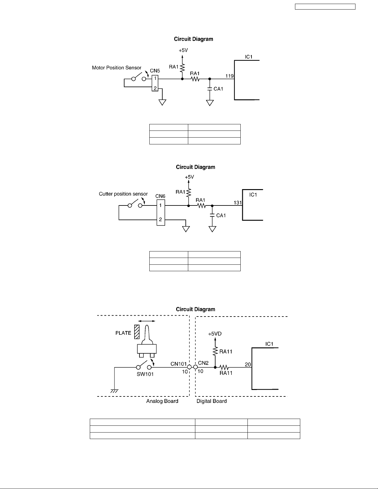
6.5.1. Motor Position Sensor
This sensor is a detection switch for recording the position of the CAM.
Signal (IC1-119 pin)
Home position Low level
Other High level
6.5.2. Cutter Position Sensor (KX-FT987 only)
KX-FT981LA-B / KX-FT987LA-B
Signal (IC1-131 pin)
Home position Low level
Other High level
6.5.3. Cover Open / Paper Sensor (SW101)
When the recording paper is loaded on the print head and the cover is closed, the paper sensor SW turns ON, and the input signal
of IC1-20 pin becomes a low level. Usually, the SW turns OFF, and the input signal of IC1-20 pin becomes a high level.
Sensor Signal (IC1-20 pin)
Set recording paper and cover is closed ON Low level
No recording paper or cover is open OFF High level
27
Page 28
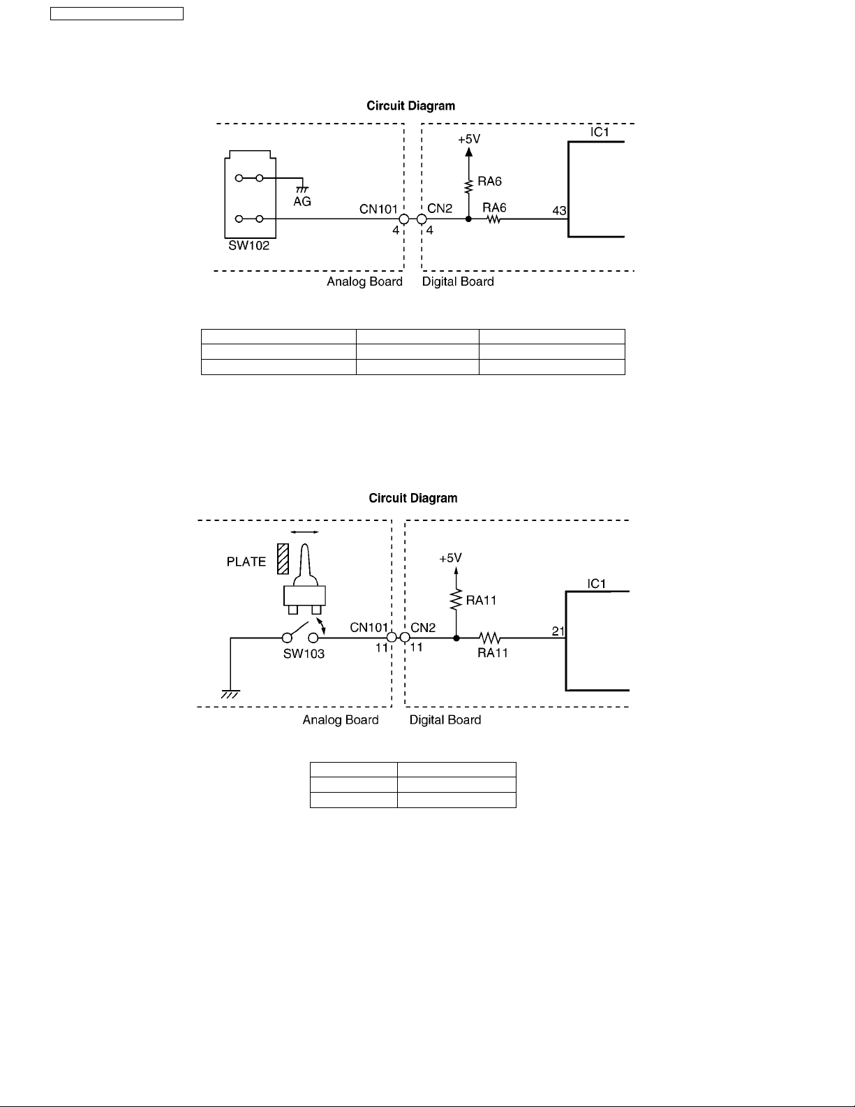
KX-FT981LA-B / KX-FT987LA-B
6.5.4. Hook Sensor (SW102)
When the handset is lifted, the switch turns ON, and the signal at pin 43 of IC1 becomes low.
When the handset is returned, the switch turns OFF, and the signal at pin 43 of IC1 becomes high.
Sensor SW Signal (IC1-43 pin)
ON-Hook OFF High level
OFF-Hook ON Low level
6.5.5. Jam Sensor (SW103)
The JAM sensor is a detection switch for determining whether the recording paper edge is in the correct position or not. If the
recording paper cannot be detected correctly at the JAM sensor position even when recording paper is present, then JAM is displayed. If the recording paper is at the sensor position, then the switch turns on the IC1-21 pin switches to a high level.
Signal (IC1-21 pin)
Paper Low level
No paper High level
28
Page 29
KX-FT981LA-B / KX-FT987LA-B
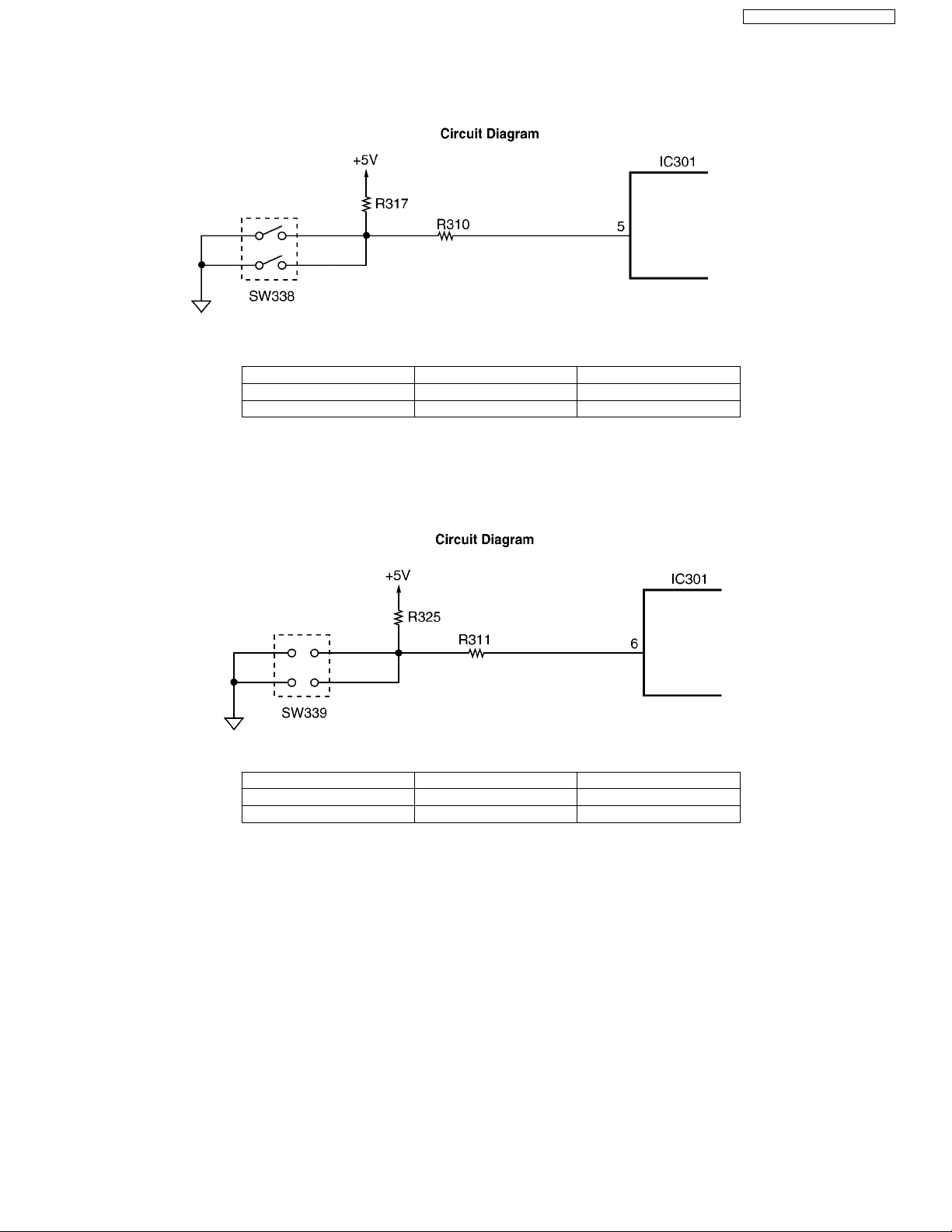
6.5.6. Document Top Sensor (SW338)
When a document is brought to the read position, the SW becomes ON, and the input signal of IC301-5 pin (Operation Board)
becomes a low level. When there is no document at the read position, the SW becomes OFF, and the input signal of IC301-5 pin
(Operation Board) becomes a high level.
Sensor SW Signal (IC301-5 pin)
Out of the Read Position OFF High level
At the Read Position ON Low level
6.5.7. Document Set Sensor (SW339)
When a document is set, the SW becomes ON, and input signal of IC301-6 pin (Operation Board) becomes a low level.
When there is no document, the SW becomes OFF, and the input signal of IC301-6 pin (Operation Board) becomes a high level.
Sensor SW Signal (IC301-6 pin)
No document OFF High level
Set document ON Low level
29
Page 30

KX-FT981LA-B / KX-FT987LA-B
6.6. Modem Section
6.6.1. Function
The unit uses a 1 chip modem (IC5) that serves as an interface between the control section for FAX transmission and reception
and the telephone line. During a transmitting operation, the digital image signals are modulated and sent to the telephone line.
During a receiving operation, the analogue image signals which are received via the telephone line are demodulated and converted into digital image signals. The communication format and procedures for FAX communication are standardized by ITU-T.
This 1 chip modem (IC5) has hardware which sends and detects all of the necessary signals for FAX communication (DTMF).
It can be controlled by writing commands from the CPU (IC1: inside ASIC) to the register in the modem (IC5).
This modem (IC5) also sends DTMF signals, generates a call tone (from the speaker), and detects a busy tone and dial tones.
Overview of Facsimile Communication Procedures (ITU-T Recommendation):
1. ON CCITT (International Telegraph and Telephone Consultative Committee)
The No. XIV Group of CCITT, one of the four permanent organizations of the International Telecommunications Union (ITU),
investigates and make recommendations on international standards for facsimiles.
2. Definition of Each Group
• Group I (G1)
Official A-4 size documents without using formats which reduce the band width of a signal are sent over telephone lines.Determined in 1968.
Transmission for about 6 minutes at a scanning line density of 3.85 lines/mm.
• Group II (G2)
Using reduction technology in the modulation/demodulation format, an A-4 size document is sent at an official scanning line density of 3.85 lines/mm for about 3 minutes.
Methods to suppress redundancy are not used.
Determined in 1976.
• Group III (G3)
Method of suppressing redundancy in the image signal prior to modulation is used. An A-4 size document is sent within about
one minute.
Determined in 1980.
• Group IV (G4)
Transmission is via the data network. A method is provided for suppressing redundancy in signals prior to transmission, and
error-free reception of transmission is possible.
The scope of these facsimile applications is not limited simply to transmission of written statements. Through symbiotic linkages
with other communication methods, it can be expected to expand to include integrated services.
30
Page 31

KX-FT981LA-B / KX-FT987LA-B
3. Facsimile Call Time Series
As shown in the following diagram, the facsimile call time series is divided into five phases.
Phase A: Call setting
Call setting can be manual/automatic.
Phase B: Pre-message procedure
Phase B is a pre-processing procedure and sequence for confirming the status of the terminal, transmission route, etc., and for
terminal control. It implements terminal preparation status, determines and displays terminal constants, confirms synchronization status, etc. and prepares for transmission of facsimile messages.
Phase C: Message transmission
Phase C is the procedure for the transmitting facsimile messages.
Phase D: Post message procedure
Phase D is the procedure for confirming that the message is completed and received. For continuous transmission, phase B or
phase C is repeated for transmission.
Phase E: Call retrieval
Phase E is the procedure for call retrieval, that is for circuit disconnection.
4. Concerning Transmission Time
Transmission Time
= Control Time + Image Transmission Time + Hold Time
Transmission time consists of the following.
Control time:
This is time at the start of transmission when the functions at the sending and receiving sides are confirmed, the transmission
mode is established, and transmission and reception are synchronized.
Image transmission time:
This is the time required for the transmission of document contents (image data). In general, this time is recorded in the catalog,
etc.
Hold time:
This is the time required after the document contents have been sent to confirm that the document was actually sent, and to
check for telephone reservations and/or the existence of continuous transmission.
5. Facsimile Standards
Telephone Network Facsimile
Item
Connection Control Mode Telephone Network Signal Mode
Terminal Control Mode T. 30 Binary
Facsimile Signal Format Digital
Modulation Mode PSK (V. 27 ter) or QAM (V. 29)
Transmission Speed 300 bps (Control Signal)
2400, 4800, 7200, 9600 bps (FAX Signal)
Redundancy Compression
Process
(Coding Mode)
Resolution Main Scan: 8 pel/mm
Line Synchronization Signal EOL Signal
1 Line Transmission Time
[ms/line]
1 dimension: MH Mode
2 dimension: MR Mode (K=2.4)
Sub Scan: 3.85, 7.7l/mm
Depends on the degree of data reduction.
Minimum Value: 10, 20
Can be recognized in 40ms.
G3 Machine
31
Page 32

KX-FT981LA-B / KX-FT987LA-B
6. Explanation of Communication and Compression Technology
a. G3 Communication Signals (T. 30 Binary Process)
For G3 Facsimile communication, this is the procedure for exchanging control signals between the sending and receiving
machines both before and after transmission of image signals.
Control signals at 300 bps FSK are: 1850 Hz...0, 1650Hz...1.
An example of a binary process in G3 communication is shown below.
Explanation of Signals
Control signals are comprised mainly of 8-bit identification signals and the data signals added to them. Data signals are added
to DIS and DCS signals.
Signal.....DIS (Digital Identification Signal)
Identification Signal Format.....00000001
Function:
Notifies the capacity of the receiving unit. The added data signals are as follows.
Signal.....DCS (Digital Command Signal)
Identification Signal Format.....X1000001
Example (Some models do not support the following items.):
Bit No. DIS/DTC DCS
1 Transmitter --- T.2 operation
2 Receiver --- T.2 operation Receiver --- T.2 operation
3 T.2 IOC = 176 T.2 IOC = 176
4 Transmitter --- T.3 operation
5 Receiver --- T.3 operation Receiver --- T.3 operation
6 Reserved for future T.3 operation features
7 Reserved for future T.3 operation features.
8 Reserved for future T.3 operation features.
9 Transmitter --- T.4 operation
32
Page 33

KX-FT981LA-B / KX-FT987LA-B
Bit No. DIS/DTC DCS
10 Receiver --- T.4 operation Receiver --- T.4 operation
11,12,13,14
0,0,0,0
0,1,0,0
1,0,0,0
1,1,0,0
0,0,1,0
0,1,1,0
1,0,1,0
1,1,1,0
0,0,0,1
0,1,0,1
1,0,0,1
1,1,0,1
0,0,1,1
0,1,1,1
1,0,1,1
1,1,1,1
Data signaling rate
V.27 ter fall back mode
V.27 ter
V.29
V.27 ter and V.29
Not used
Reserved
Not used
V.27 ter and V.29 and V.33
Not used
Reserved
Not used
V.27 ter and V.29 and V.33 and V.17
Not used
Reserved
Not used
Reserved
Data signaling rate
2400 bit/s, V.27 ter
4800 bit/s, V.27 ter
9600 bit/s, V.29
7200 bit/s, V.29
14400 bit/s, V.33
12000 bit/s, V.33
Reserved
Reserved
14400 bit/s, V.17
12000 bit/s, V.17
9600 bit/s, V.17
7200 bit/s, V.17
Reserved
Reserved
Reserved
Reserved
15 R8×7.7 lines/mm and/or 200×200 pels/25.4mm R8×7.7 lines/mm and/or 200×200 pels/25.4mm
16 Two-dimensional coding capability Two-dimensional coding capability
17, 18
(0, 0)
(0, 1)
Recording width capabilities
1728 picture elements along scan line length of
215 mm ± 1%
1728 picture elements along scan line length of
215 mm ± 1%
Recording width
1728 picture elements along scan line length of
215 mm ± 1%
2432 picture elements along scan line length of
303 mm ± 1%
2048 picture elements along scan line length of
255 mm ± 1%
2432 picture elements along scan line length of
303 mm ± 1%
(1, 0)
1728 picture elements along scan line length of
215 mm ± 1%
2048 picture elements along scan line length of
255 mm ± 1%
2048 picture elements along scan line length of
255 mm ± 1%
(1, 1)
19, 20
(0, 0)
(0, 1)
(1, 0)
(1, 1)
21, 22, 23
(0, 0, 0)
(0, 0, 1)
(0, 1, 0)
(1, 0, 0)
(0, 1, 1)
(1, 1, 0)
(1, 0, 1)
(1, 1, 1)
Invalid
Maximum recording length capability
A4 (297 mm)
Unlimited
A4 (297 mm) and B4 (364 mm)
Invalid
Minimum scan line time capability of the receiver
20 ms at 3.85 l/mm: T
40 ms at 3.85 l/mm: T
10 ms at 3.85 l/mm: T
5 ms at 3.85 l/mm: T
10 ms at 3.85 l/mm: T
20 ms at 3.85 l/mm: T
40 ms at 3.85 l/mm: T
0 ms at 3.85 l/mm: T
= T
7.7
= T
7.7
= T
7.7
= T
7.7
= 1/2 T
7.7
= 1/2 T
7.7
= 1/2 T
7.7
= T
7.7
3.85
3.85
3.85
3.85
3.85
3.85
3.85
3.85
Invalid
Maximum recording length
A4 (297 mm)
Unlimited
B4 (364 mm)
Invalid
Minimum scan line time
20 ms
40 ms
10 ms
5 ms
0 ms
24 Extend field Extend field
25 2400 bit/s handshaking 2400 bit/s handshaking
26 Uncompressed mode Uncompressed mode
27 Error correction mode Error correction mode
28 Set to "0". Frame size 0 = 256 octets 1 = 64 octets
29 Error limiting mode Error limiting mode
30 Reserved for G4 capability on PSTN Reserved for G4 capability on PSTN
31 T.6 coding capability T.6 coding enabled
32 Extend field Extend field
33
(0)
(1)
Validity of bits 17, 18
Bits 17, 18 are valid
Bits 17, 18 are invalid
34 Recording width capability 1216 picture elements along
Recording width
Recording width indicated by bits 17, 18
Recording width indicated by this field bit information
Middle 1216 elements of 1728 picture elements
scan line length of 151 ± mm 1%
35 Recording width capability 864 picture elements along scan
Middle 864 elements of 1728 picture elements
line length of 107 ± mm 1%
36 Recording width capability 1728 picture elements along
Invalid
scan line length of 151 ± mm 1%
37 Recording width capability 1728 picture elements along
Invalid
scan line length of 107 ± mm 1%
38 Reserved for future recording width capability.
33
Page 34

KX-FT981LA-B / KX-FT987LA-B
Bit No. DIS/DTC DCS
39 Reserved for future recording width capability.
40 Extend field Extend field
41 R8×15.4 lines/mm R8×15.4 lines/mm
42 300×300 pels/25.4 mm 300×300 pels/25.4 mm
43 R16×15.4 lines/mm and/or 400×400 pels/25.4 mm R16×15.4 lines/mm and/or 400×400 pels/25.4 mm
44 Inch based resolution preferred Resolution type selection
"0": neritic based resolution
"1": inch based resolution
45 Metric based resolution preferred Don’t care
46 Minimum scan line time capability for higher resolutions
= T
"0": T
15.4
"1": T
7.7
15.4
= 1/2T
7.7
Don’t care
47 Selective Polling capability Set to "0".
48 Extend field Extend field
Note 1 - Standard facsimile units conforming to T.2 must have the following capability: Index of cooperation (IOC)=264.
Note 2 - Standard facsimile units conforming to T.3 must have the following capability: Index of cooperation (IOC)=264.
Note 3 - Standard facsimile units conforming to T.4 must have the following capability: Paper length=297 mm.
Signal Identification Signal Format Function
Training 1 ——————— A fixed pattern is transmitted to the receiving side at a speed (2400
bps to 9600 bps) designated by DCS, and the receiving side opti-
mizes the automatic equalizer, etc., according to this signal.
TCF
(Training Check)
CFR
X0100001 Notifies the sending side that TCF has been properly received. If
(Confirmation to Receive)
Training 2 ——————— Used for reconfirming the receiving side like training 1.
Image Signal Refer to the next page. ———————
RTC
(Return to Control)
EOP
X1110100 End of one communication
(End of Procedure)
MCF
X0110001 End of 1 page reception
(Message Confirmation)
DCN
X1011111 Phase E starts.
(Disconnect)
MPS
X1110010 Completion of transmission of 1 page. If there are still more docu(Multi-Page Signal)
PRI-EOP
X1111100 If there is an operator call from the sender, it is output after RTC.
(Procedural Interrupt-EOP)
PIP
X0110101 This is output when an operator call is received.
(Procedural Interrupt Positive)
——————— Sends 0 continuously for 1.5 seconds at the same speed as the
training signal.
TCF is not properly received, FTT (Failure To Train) X0100010 is
relayed to the sender. The sender then reduces the transmission
speed by one stage and initiates training once again.
——————— Sends 12 bits (0...01 × 6 times) to the receiver at the same speed as
the image signal and notifies completion of transmission of the first
sheet.
ments to be sent, they are output instead of EOP. After MCF reception, the sender transmits an image signal of the second sheet.
34
Page 35

b. Redundancy Compression Process Coding Mode
This unit uses one-dimensional MH format.
KX-FT981LA-B / KX-FT987LA-B
35
Page 36

KX-FT981LA-B / KX-FT987LA-B
6.6.2. Modem Circuit Operation
The modem (IC5) has all the hardware satisfying the CCITT standards mentioned previously.
When the ASIC IC1 (61) is brought to a low level, the modem (IC5) is chip-selected and the resistors inside IC are selected by the
select signals from ASIC (IC1) ADR0-ADR4. The commands are written through the data bus, and all the processing is controlled
by the ASIC (IC1) according to CCITT procedures. The INT signal dispatched from IRQ (pins 100 of IC5) to ASIC (IC1) when the
transmission data is accepted and the received data is demodulated, the ASIC (IC1) implements post processing. This modem
(IC5) has an automatic application equalizer.
With training signal 1 or 2 during G3 reception, it can automatically establish the optimum equalizer. The modem (IC5) operates
using the 32.256 MHz clock (X3).
1. Facsimile Transmission
The digital image data on the data bus is modulated in the modem (IC5), and sent from pin 56 via Analog SW IC10, amplifier
IC9 and the NCU section to the telephone line.
Refer to Check Sheet for Signal Route (P.114).
2. Facsimile Reception
The analog image data which is received from the telephone line passes through the NCU section and enters pin 47 of the
modem (IC5). The signals that enter pin 47 of the modem (IC5) are demodulated in the board to digital image signals, then
placed on the data bus.
In this case, the image signals from the telephone line are transmitted serially. Hence, they are placed on the bus in 8 bit
units. Here, the internal equalizer circuit reduces the image signals to a long-distance receiving level.
This is designed to correct the characteristics of the frequency band centered about 3 kHz and maintain a constant receiving
sensitivity. It can be set in the service mode.
Refer to Check Sheet for Signal Route (P.114).
3. DTMF Transmission (Monitor tone)
The DTMF signal generated in the modem (IC5) is output from pin 56, and is then sent to the circuit on the same route as
used for facsimile transmission.
Refer to Check Sheet for Signal Route (P.114).
(DTMF Monitor Tone)
Refer to Check Sheet for Signal Route (P.114).
4. Call Tone Transmission
This is the call signal which is generated in the ASIC (IC1) and sent to the speaker.
Refer to Check Sheet for Signal Route (P.114).
5. Busy/Dial Tone Detection
The path is the same as FAX receiving. When it is detected, the carrier detect bit of the resistor in the modem (IC5) becomes
1, and this status is monitored by the ASIC (IC1).
6. Caller ID Detection
The caller ID signal which is received from the telephone line enters pin 50 of the modem (IC5).
36
Page 37

KX-FT981LA-B / KX-FT987LA-B
6.7. NCU Section
6.7.1. General
It is composed of bell detection circuit, pulse dial circuit, line amplifier, sidetone circuits.
6.7.2. Bell Detection Circuit
1. Circuit Operation
The signal waveform for each point is indicated below. The signal (low level section) input to pin 19 of ASIC IC1 on the digital
board.
TEL LINE → PC102 (1, 2 → 4) → CN101 (9) → {CN2 (9) → IC1 (19)}
Note:{ } : inside the digital board
6.7.3. ON/OFF Hook Circuit
Normally (ON-HOOK condition), LINE RELAY (RLY101) is OFF. While OFF-HOOK, RLY101 turns ON. This LINE RELAY is controlled by pin 130 of IC1 through the Q7.
ON-HOOK:
IC1 (130) Low Level → Q7 OFF → RLY101 OFF
OFF-HOOK:
IC1 (130) High Level → Q7 ON → RLY101 ON
6.7.4. Pulse Dial Circuit
Make state:
IC1 (130) High Level → Q7 ON → RLY101 ON
Break state:
IC1 (130) Low Level → Q7 OFF → RLY101 OFF
37
Page 38

KX-FT981LA-B / KX-FT987LA-B
6.7.5. Line Amplifier and Side Tone Circuits
1. Circuit Operation
The reception signal received as output from line transformer T101 is given as input to C108, R109 and IC101(2).
Then it is input to the reception system at an amplifier gain of 2.5 dB from pin (2).
The transmission signal is input from CN101 pin (6), and output to the TEL line through T101. Without a side tone circuit, the
transmission signal would return to the reception amplifier via C113 and R114. Here, the signal output from CN101 pin (6)
passes through C113, R113, R112, C109 and R110, and enters the amplifier IC101 pin (2). This is used to cancel the return
portion of the transmission signal. This is the side tone circuit.
38
Page 39

KX-FT981LA-B / KX-FT987LA-B
6.7.6. Calling Line Identification Circuit
1. Function
This unit is compatible with the Caller ID service offered by your local telephone company. To use this feature, you must subscribe to a Caller ID service. The data for the caller ID from the telephone exchange is sent during the interval between the
first and second rings of the bell signal. The data from the telephone exchange is a modem signal which is modulated in an
FSK (Frequency Shift Keying) format. Data "0" is a 1200 Hz sine wave, and data 1 a 2200 Hz sine wave.
There are two type of the message format which can be received:i.e.the single data message format and multiple data message format.
The multiple data format allows to transmit the name and data code information in addition to the time and telephone number
data.
When there is multiple data in the unit, the name or telephone number are displayed.
2. Circuit Operation:
The caller ID signal input from TEL LINE is processed with MODEM IC5.
Refer to Check Sheet for Signal Route (P.114) for the route of caller ID signal.
39
Page 40

KX-FT981LA-B / KX-FT987LA-B
6.7.7. Calling Line Identification Circuit (DTMF)
1. Function
This unit is compatible with the Caller ID service offered by your local telephone company. To use this feature, you must subscribe to a Caller ID service. The data for the Caller ID from the telephone exchange is sent before the first ring signal. The
data from the telephone exchange is sent by DTMF signal.
2. Circuit Operation:
The Caller ID signal from TEL LINE is processed with MODEM (IC5).
Refer to Check Sheet for Signal Route (P.114) for the route of Caller ID (DTMF) signal.
40
Page 41

KX-FT981LA-B / KX-FT987LA-B
6.8. ITS (Integrated Telephone System) and Monitor Section
6.8.1. General
The general ITS operation is performed by the modem IC5. The alarm tone, the key tone, the calling tone and the beep are output
from the ASIC IC1 (digital board).
6.8.2. Telephone Monitor (KX-FT981 only)
1. Function
This is the function when you are not holding the handset and can hear the caller’s voice from the line.
2. Signal path
Refer to Check Sheet for Signal Route (P.114)
6.8.3. Speakerphone Circuit (KX-FT987 only)
1. Function
The circuit controls the automatic switching of the transmitted and received signals, to and from the telephone line, when the
unit is used in the hands-free mode.
2. Circuit Operation
The speakerphone can only provide duplex.
3. Signal path
Refer to Check Sheet for Signal Route (P.114)
6.8.4. Handset Circuit
1. Function
This circuit controls the conversation over the handset, i.e. the transmitted and received voices to and from the handset.
2. Signal path
Refer to Check Sheet for Signal Route (P.114)
6.8.5. Monitor Circuit for Each Signals
1. Function
This circuit monitors various tones, such as 1 DTMF tone, 2 Alarm/Beep/Key tone/Bell 3 Dummy ring back tone.
2. Signal path
Refer to Check Sheet for Signal Route (P.114)
6.9. TAM Interface Section (KX-FT981 only)
1. Function
When TAM is connected to this unit, the unit receives documents for FAX calls or the external TAM records a voice message
automatically.
2. Circuit Operation
The TAM INTERFACE circuit consists of a CNG signal from the other party’s detection circuit, VOX detection circuit (to judge
sound/no-sound) and RLY101 (to separate EXT. TAM).
a. CNG/VOX signal detection circuit
The CNG signal from the other party’s FAX is detected in MODEM IC5 (digital board).
b. Remote receiving
This is the parallel connected DTMF signal for the TEL mode between a and b. When the other party is a FAX, the unit
changes to FAX receiving.
3. Signal path
Refer to Check Sheet for Signal Route (P.114)
41
Page 42

KX-FT981LA-B / KX-FT987LA-B
6.10. ATAS (Automatic Telephone Answering System) Section
(KX-FT987 only)
1. Function
The ATAS main operation is performed by the special IC5 (MODEM). IC6 (FLASH MEMORY) control signals are input from
ASIC IC1.
a. Greeting/Message Recording
b. ICM Recording
c. Greeting/Message/ICM play to speaker
d. Greeting/Message/ICM play to Tel Line
e. Vox Detection
2. Signal Path
Refer to Check Sheet for Signal Route (P.114)
42
Page 43

KX-FT981LA-B / KX-FT987LA-B
6.11. Operation Board Section
The unit consists of a LCD (Liquid crystal display), KEYs and LEDs (light-emitting diodes). They are controlled by the Gate Array
(IC301) and ASIC (IC1: on the DIGITAL BOARD). The key matrix table is shown below.
LCD
(Chip on board type)
ASIC
IC1
CN7
CN301
CN302
KSL0~4
GATE ARRAY
IC301
8 x 5
KIN0~7
XLED8, 9
XLED13
DOCUMENT TOP SENSOR
DOCUMENT SET SENSOR
DIGITAL BOARD OPERATION BOARD
KX-FT981 / KX-FT987: OPERATION BOARD: BLOCK DIAGRAM
KEYS
MATRIX
LED
D301
43
Page 44

KX-FT981LA-B / KX-FT987LA-B
6.12. LCD Section
The Gate Array IC(IC301) works only for writing the ASCII code from the data bus (D4~D7). V0 is supplied for the crystal drive.
R312, R313, R314 and R316 are density control resistors.
Consequently, in this unit, the timing (positive clock) is generated by the LCD interface circuitry in the gate array (IC301).
English font
(Global)
2 lines
DIsplay mode Density Normal Dark
LED1 (IC301-22pin) H L
LED15 (IC301-21pin) L L
LED14 (IC301-20pin) Hi-Z L
44
Page 45

6.13. Power Supply Board Section
This power supply board uses the switching regulator method.
KX-FT981LA-B / KX-FT987LA-B
[Input Circuit]
The input current goes into the input rectifier circuit through the filter circuit. The filter circuit decreases the noise voltage and the
noise electric field strength.
[Rectifier Circuit]
The input current is rectified by D101,D102,D103 and D104 and charges C106 to make DC voltage. Then it supplies power to the
converter circuit.
[Kick-on voltage circuit]
Bias is applied to the Q101 gate via this circuit when the AC power is turned on and Q101 begins operating.
45
Page 46

KX-FT981LA-B / KX-FT987LA-B
The following is an overview of how the power supply unit is controlled.
The control method of this power supply unit is pulse width modulation.
When Q1 is ON, the energy is charged in the transfer primary coil according to E1. When Q1 is OFF, the energy is output from the
secondary transfer as follows.
L → D
→ Load → L
1
Then the power is supplied to the Load. When Q1 is ON, power is not output from the secondary side. The output voltage is fed
back in the control IC according to the error amp rectifier. Then depending on how T
is controlled, stabilization occurs. Also,
ON
when the current load becomes too large, in order to decrease the voltage output, the increase in is controlled and the output
voltage is stabilized.
Therefore, basically the timing: Ton/Toff of Q1 controls the output voltage.
46
Page 47

KX-FT981LA-B / KX-FT987LA-B
[Surge Absorber Circuit]
This circuit is for absorbing surge voltage generated by the transformer.
[Control Circuit and Detecting Circuit]
The control circuit amplifies the output with increased voltage detected in the error detecting circuit. Then it drives the main transistor.
In this power supply, the duty ratio is defined by changing the ON period of the main transistor.
This is shown as follows.
When the output voltage of the 24V circuit increases, the current of the photo coupler PC101 increases, the pulse width of the output control IC becomes narrower and the ON period of Q101 becomes shorter.
[Over Current Limiter (O.C.L)]
The highest drain current (Q101) is limited by a limiter circuit (IC101) of 24V. The 24V output is limited by this circuit.
[Over Voltage Circuit]
If the 24V output increases because the error detecting circuit or control circuit is broken, IC101 will recognize this signal and output
becomes 0V.
Dummy load method (to quickly check the power supply output)
Refer to Power Supply Board Section (P.119).
47
Page 48

KX-FT981LA-B / KX-FT987LA-B
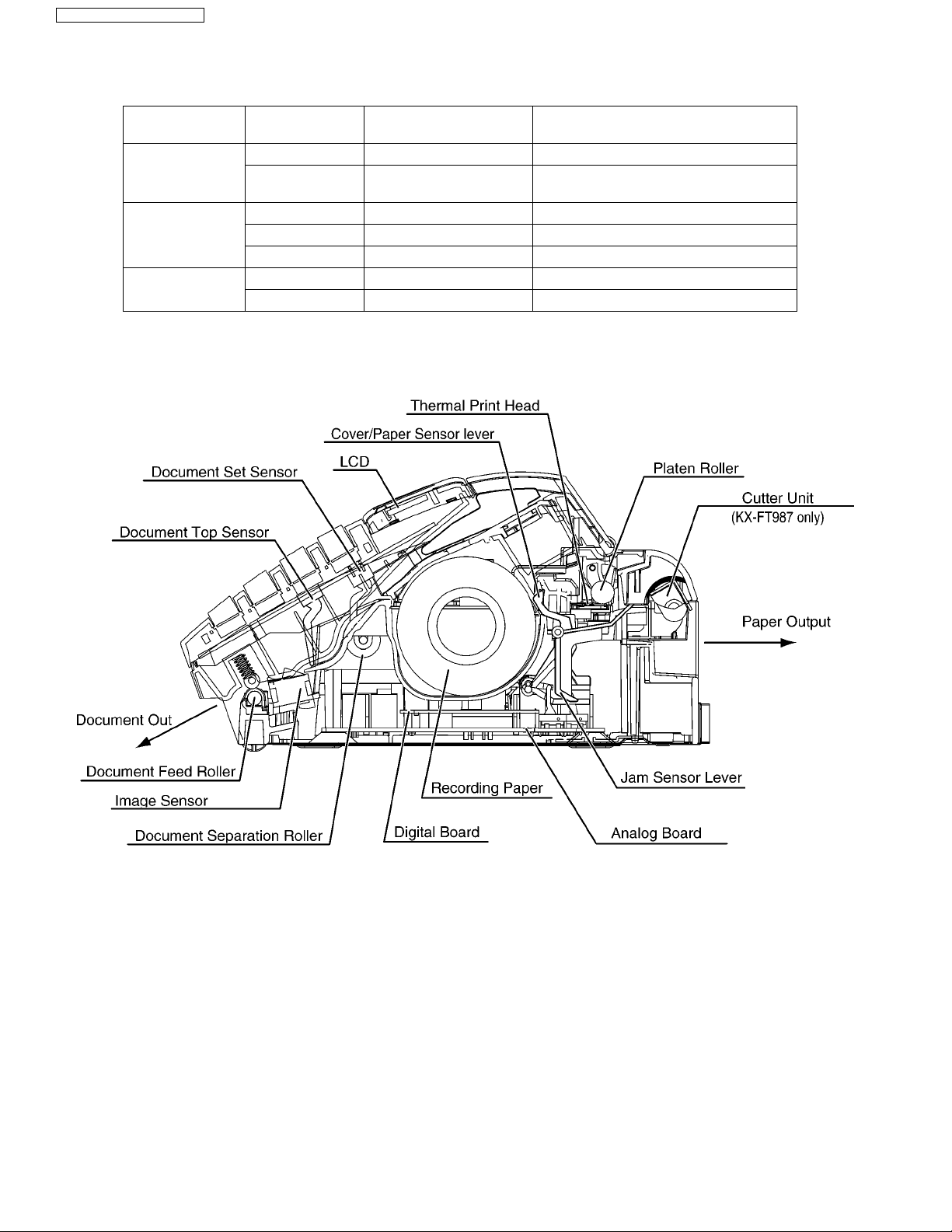
7 Location of Controls and Components
7.1. Overview
(1) Speaker
(2) Document guides
(3) Paper stacker (KX-FT987 only)
(4) Document feeder tray
(5) Top cover
(6) Document exit
(7) Document entrance
(8) Top cover release button
7.2. Control Panel
(1) [CALLER ID]
• To use Caller ID features.
(2) [STOP]
• To stop an operation or programming session.
• To erase a character/number. Press and hold to erase all
characters/numbers.
(3) [FLASH]
• To access special telephone services or for transferring
extension calls.
(4) [REDIAL/PAUSE]
• To redial the last number dialled. If the line is busy when
you send a fax, the unit will automatically redial the number up to 2 times.
• To insert a pause during dialing.
(5) [RECORD] (KX-FT987 only)
• To record your greeting message.
• To record a voice memo.
(6) [ERASE] (KX-FT987 only)
• To erase messages.
• To erase a stored item.
(7) [PLAYBACK] (KX-FT987 only)
• To play messages.
(8) [AUTO ANSWER]
• To turn the auto answer setting ON/OFF.
48
Page 49

(9) Station keys
• To use one-touch dial feature.
(10) [FAX/START]
• To start sending or receiving a fax.
(11) [COPY]
• To copy a document.
(12) [MIC] (KX-FT987 only)
• The built-in microphone.
(13) [TONE]
• To change from pulse to tone temporarily during dialling
when your line has rotary pulse services.
(14) [HANDSET MUTE] (KX-FT981 only)
[MUTE] (KX-FT987 only)
• To mute your voice during a conversation. Press again to
resume the conversation.
(15) [MONITOR] (KX-FT981 only)
• To initiate dialling without lifting the handset.
(16) [DIGITAL SP-PHONE] (KX-FT987 only)
• For speakerphone operation.
(17) [BROADCAST]
• To transmit a document to multiple parties.
(18) Navigator/ [VOLUME] [PHONEBOOK]
• To search for a stored item.
• To select features or feature settings during programming.
• To adjust volume.
• To open a phonebook.
(19) [SET]
• To store a setting during programming.
(20) [MENU]
• To initiate or exit programming.
(21) [LOWER]
• To select stations 6-10 for the one-touch dial feature.
KX-FT981LA-B / KX-FT987LA-B
8 Installation Instructions
8.1. Installation Space
The space required to install the unit is shown below.
The dimensions given are necessary for the unit to operate
efficiently.
Note:
• Avoid excessive heat or humidity.
• Use the unit within the following ranges of temperature and
humidity.
• Ambient temperature: 5°C to 35°C
• Relative humidity: 20% to 80% (without condensation)
• Power cord length should be less than 5 meters. Using a
longer cord may reduce the voltage or cause malfunctions.
• Avoid direct sunlight.
• Do not install near devices which contain magnets or generate magnetic fields.
• Do not subject the unit to strong physical shock or vibration.
• Keep the unit clean. Dust accumulation can prevent the unit
from functioning properly.
• To protect the unit from damage, hold both sides when you
move it.
49
Page 50

KX-FT981LA-B / KX-FT987LA-B
8.2. Connections
Important:
• The unit will not function when there is a power failure.
To make calls in emergency situations, you should connect a telephone that can function during a power failure to the telephone line.
(1) Paper stacker (KX-FT987 only)
• Make sure the paper stacker must not touch the wall.
(2) Power cord
• Connect to the power outlet (120 V, 60 Hz).
(3) Telephone line cord
• Connect to [LINE] jack and a single telephone line jack.
(4) [EXT] jack (KX-FT981 only)
• Remove the stopper if attached.
(5) Handset cord
(6) Extension telephone (not included)
8.3. Installing the Recording Paper
1. Open the top cover by pressing the top cover release but-
ton ( ).
2. Install the recording paper.
Caution:
• When you operate this product, the power outlet should
be near the product and easily accessible.
• Keep the unit away from walls as far as possible to pre-
vent a recording paper jam.
Note:
Before you can make calls, the dialling mode setting may
need to be changed.
3. Insert the leading edge of the paper into the opening
above the thermal head ( ).
4. Pull the paper out of the unit.
50
• Make sure that there is no slack in the paper roll.
Page 51

5. Close the top cover securely by pushing down on both
sides.
6. For KX-FT981:
Press [FAX/START], then tear off the excess paper by
pulling it towards you.
KX-FT981LA-B / KX-FT987LA-B
8.4. Documents the Unit can Send
For KX-FT987:
Press [FAX/START] to cut the paper.
Note:
• If the paper is secured with glue or tape, cut approximately 15 cm from the beginning of the roll before installing it.
• When the power cord is connected, a message is printed
each time the top cover is opened then closed. If the
recording paper is installed upside down, the message
will not be printed. Install the paper correctly.
• For accessory information, see Optional Accessories
(P.9).
Document weight
• Single sheet: 45 g/m
2
to 90 g/m
• Multiple sheets: 60 g/m2 to 80 g/m
2
2
Note:
• Remove clips, staples or other fasteners.
• Do not send or copy documents that are on the following
types of paper: (Make a copy of the document using another
copier and send the copy.)
— Chemically treated paper such as carbon or carbonless
duplicating paper
— Electrostatically charged paper
— Badly curled, creased or torn paper
— Paper with a coated surface
— Paper with a faint image
— Paper with printing on the opposite side that can be seen
through the other side, such as newsprint.
• Check that ink, paste or correction fluid has dried completely.
• To send a document with a width of less than 210 mm, we
recommend using a copy machine to copy the original document onto A4 or letter-sized paper, then sending the copied
document.
51
Page 52

KX-FT981LA-B / KX-FT987LA-B
9 Operating Instructions
9.1. Setting Logo
Your logo will be printed on the top of each page sent from your
unit. The logo can be your name or the name of your company.
Refer to Translation Lists (P.9) for display.
1. Press [MENU].
To select characters with dial keypad
2. Press [] or [] repeatedly to display the following.
3. Press [SET].
• The cursor ( ) will appear on the display.
4. Enter your logo, up to 30 characters. See the following
character table for details.
5. Press [SET].
• The next feature will be displayed.
6. Press [MENU].
Note:
To enter another character that is located on the same dial
key, press [] to move the cursor to the next space.
To enter your logo
Example: “BILL“
1. Press [2] 4 times.
2. Press [4] 3 times.
3. Press [5] 3 times.
4. Press [] to move the cursor to the next space and
press [5] 3 times.
52
Page 53

To change uppercase or lowercase letters
Pressing the [] button will change to uppercase or lower-
case letters alternately.
1. Press [2] 4 times.
2. Press [4] 3 times.
3. Press [].
4. Press [5] 3 times.
To correct a mistake
1. Press [] or [] to move the cursor to the incorrect
character.
2. Press [STOP].
• To erase all characters, press and hold [STOP].
3. Enter the correct character.
KX-FT981LA-B / KX-FT987LA-B
53
Page 54

KX-FT981LA-B / KX-FT987LA-B
10 Test Mode
The codes listed below can be used to perform simple checks for some of the unit’s functions. When complaints are received
from customers, they provide an effective tool for identifying the locations and causes of malfunctions. To do this, you set the
Service mode (Refer to Operation Flow (P.58).) first, then operate the below test items.
Test Mode Type of Mode Code Function
Operation after code
input
MEMORY CLEAR Service Mode [5] [5] [0] Refer to Memory Clear Specification (P.61).
[SET]
FLASH MEMORY
CHECK
DTMF SINGLE TONE
TEST
MODEM TEST Service Mode [5] [5] [4] Telephone line circuit is connected automatically, output the following signals on
SCAN TEST Service Mode [5] [5] [5] Turns on the LEDs of the CIS and operates the read systems.
MOTOR TEST Service Mode [5] [5] [6] Rotates the transmission and reception motor to check the operation of the motor.
Service Mode [5] [5] [1] Indicates the version and checks the sum of the FLASH MEMORY.
[SET]
Service Mode [5] [5] [2] Outputs the DTMF as single tones. Used to check the frequencies of the individ-
[1]: ON
[2]: OFF
[SET]
[SET]
[SET]
ual DTMF tones. Refer to DTMF Single Tone Transmit Selection (P.56).
the circuit line.
1) OFF 2) 9600bps 3) 7200bps 4) 4800bps 5) 2400bps 6) 300bps 7) 2100Hz
8) 1100Hz
Refer to CIS (Contact Image Sensor) Section (P.125).
02: FAX TX / Reading memory
06: Cutter (KX-FT987 only)
08: Recording paper is fed
10: Copy
13: Recording Paper reverse
Press [STOP] button to quit.
LED TEST Service Mode [5] [5] [7] All LEDs above the operation panel board flash on and off, or are illuminated.
[SET]
LCD TEST Service Mode [5] [5] [8] Checks the LCD indication.
[SET]
KEY TEST Service Mode [5] [6] [1] Checks the key operation except [STOP] key.
The available key is
any one that except
[STOP] key.
CUTTER TEST
(KX-FT987 only)
MEMORY CLEAR
(except History data)
VOICE PROMPT TEST
(KX-FT987 only)
Service Mode [5] [6] [2] Perform cutter test 10 times.
[SET]
Service Mode [7] [1] [0] Refer to Memory Clear Specification (P.61).
[SET]
Service Mode [7] [8] [4] You can hear the voice prompt from speaker after pressing “SET” key.
[SET]
Illuminates all the dots to check if they are normal.
Refer to No LCD Indication (P.122).
Indicates the button code on the LCD while the button is pressed, see Button
Code Table (P.56)
Refer to No Key Operation (P.122).
54
Page 55

Test Mode Type of Mode Code Function
Operation after code
input
SENSOR TEST &
VOX TEST
Service Mode [8] [1] [5] If you enter this mode and operate sensor levers with your hands, the LCD display
[SET]
of the related sensor (or switch) turns ON / OFF. Also, when copying a document,
the related sensor will turn ON / OFF.
For each sensor’s operation, refer to Sensors and Switches (P.26).
LCD DISPLAY
Do: Document set sensor
Paper inserted. Turns on when a document is inserted.
Sn: Document top sensor.
At the read position, turns on when the front cover is opened and the sensor
lever is pressed directory.
Co: Cover open sensor
Turns on and off when the front cover is opened and closed.
Jm: JAM sensor
When JAM sensor is on “Jm” functions.
Ct: Cutter sensor (KX-FT987 only)
When cutter sensor is on “Ct” functions.
Vx: Vox signal (KX-FT987 only)
:Detection signal for the tone on the line. Turns on when there is a tone signal
on the line
Note:
• Press [STOP] button to quit.
DIGITAL
SPEAKERPHONE
RX & TX CHECK
(KX-FT987 only)
PRINT TEST
PATT ERN
Service Mode [8] [4] [1] Refer to Digital Speakerphone (KX-FT987 only) (P.117).
SPEAKERPHONE
Service Mode [8] [5] [2] Prints out the test pattern.
[SET]
You can select 1~4. (See Print Test Pattern (P.57))
KX-FT981LA-B / KX-FT987LA-B
55
Page 56

KX-FT981LA-B / KX-FT987LA-B
10.1. DTMF Single Tone Transmit Selection
When set to ON (=1), the 12 keys and transmission frequencies are as shown.
When set to OFF (=2), the 12 keys and transmission frequencies are as shown.
key High Frequency (Hz) key Low Frequency (Hz)
“1” 697 “5” 1209
“2” 770 “6” 1336
“3” 852 “7” 1477
“4” 941 “8” 1633
Note:
After performing this check, do not forget to turn the setting off.
Otherwise, dialing in DTMF signal will not work.
10.2. Button Code Table
Code Button Name Code Button Name Code Button Name
04 FAX /START 31 1 47 CALLER ID
05 LOWER 32 2
06 COPY 33 3 64 STATION KEY 1
08 MONITOR or SP-PHONE 34 4 65 STATION KEY 2
09 BROADCAST 35 5 66 STATION KEY 3
0A HANDSET MUTE or MUTE 36 6 67 STATION KEY 4
0C AUTO ANSWER 37 7 68 STATION KEY 5
0D SET 38 8
1E
[ ] NEXT
1F
[ ] PREV
14 RECORD (KX-FT987 only) 3C #
16 ERASE (KX-FT987 only) 3D REDIAL/PAUSE
18 PLAYBACK (KX-FT987 only) 3E FLASH (RECALL)
39 9
3A 0 00 NO INPUT
3B -- STOP
High (Hz) 1209 1336 1477
Low (Hz)
697 “1” “2” “3”
770 “4” “5” “6”
852 “7” “8” “9”
941
“”
“0” “#”
20 MENU
25 [ + ] VOLUME
26 [—] VOLUME
56
Page 57

10.3. Print Test Pattern
KX-FT981LA-B / KX-FT987LA-B
1. Platen roller
3. Thermal head 1 dot
2. Left margin / Top margin
4. Use this test pattern to confirm the platen roller timing.
57
Page 58

KX-FT981LA-B / KX-FT987LA-B
11 Service Mode
The programming functions are used to program the various features and functions of the machine, and to test the machine.
This facilitates communication between the user and the service man while programming the unit.
11.1. Programing and Lists
11.1.1. Operation
There are 2 basic categories of programming functions, the User Mode and the Service Mode. The Service Mode is further broken down into the normal and special programs. The normal programs are those listed in the Operating Instructions and are
available to the user. The special programs are only those listed here and not displayed to the user. In both the User and Service Modes, there are Set Functions and Test Functions. The Set Functions are used to program various features and functions,
and the Test Functions are used to test the various functions. The Set Functions are accessed by entering their code, changing
the appropriate value, then pressing the SET key. The Test Functions are accessed by entering their code and pressing the key
listed on the menu. While programming, to cancel any entry, press the STOP key.
11.1.2. Operation Flow
Refer to Translation Lists (P.9) for display.
58
Page 59

11.1.3. Service Function Table
KX-FT981LA-B / KX-FT987LA-B
Code Function Set Value Effective
Range
501 Pause time × 100 msec 001~600 030 ----------
503 Dial speed select 1: 10 pps
2: 20 pps
510 VOX time (KX-FT987 only) 1:6 sec
511 VOX sensitivity (KX-FT987 only)
512 VOX mode Detection (KX-FT987 only) 1: A
514 Bell detection time × 100 msec 1~9 6 ----------
520 CED frequency select 1: 2100 Hz
521 International mode select 1: ON
522 Auto standby select 1: ON
523 Receive equalizer select 1: 0 km
524 Transmission equalizer select 1: 0 km
544 Document feed position × mm 1~9 5 When the ADF function is in correct, adjust the feed
550 Memory Clear See Memory Clear Specification (P.61).
551 Flash memory check See Test Mode (P.54).
552 DTMF single tone test 1: ON
553 Monitor on FAX communication select 1: OFF
554 Modem test See Test Mode (P.54).
555 Scan test See Test Mode (P.54).
556 Motor test See Test Mode (P.54).
557 LED test See Test Mode (P.54).
558 LCD test See Test Mode (P.54).
559 Document jam detection select 1: ON
560 Cutter selection
(KX-FT987 only)
561 KEY test See Test Mode (P.54).
562 Cutter test (KX-FT987 only) See Test Mode (P.54).
567 T0 timer × second 001~255 046 ----------
570 BREAK % select 1: 61%
571 ITS auto redial time set × number of
572 ITS auto redial line disconnection time
set
2:4 sec
1: High
2: Low
2: B
2: 1100 Hz
2: OFF
2: OFF
2: 1.8 km
3: 3.6 km
4: 7.2 km
2: 1.8 km
3: 3.6 km
4: 7.2 km
2: OFF
2: PHASE B
3: ALL
2: OFF
1: ON
2: OFF
2: 67%
times
× second 001~999 065 Sets the interval of ITS redialing.
1, 2 1 ----------
1, 2 1 Setting of the end of call confirmation VOX.
1, 2 1 When the TAM (or EXT TAM) does not stop recording
1, 2 1 ----------
1, 2 1 See Symptom/Countermeasure Table for long distance
1, 2 1 See Symptom/Countermeasure Table for long distance
1, 2 1 The resolution reverts to the default when transmission
1~4 1 When the telephone station is far from the unit or recep-
1~4 1 When the telephone station is far from the unit or trans-
1, 2 2 See Test Mode (P.54).
1~3 1 Sets whether to monitor the line signal with the unit's
1, 2 1 Sets whether or not to detect a paper jam. If a docu-
1, 2 1 Turns off the cutter function.
1, 2 1 Sets the % break of pulse dialing according PBX.
00~99 00 Selects the number of times that ITS is redialed (not
Default Remarks
the ICM because noise is detected on the telephone
line, change this setting to “LOW”.
and international calls in The unit can copy, but can-
not transmit/receive (P.87).
and international calls in The unit can copy, but can-
not transmit/receive (P.87).
is complete.
tion cannot be performed correctly, adjust accordingly.
mission cannot be performed correctly, adjust accordingly.
position.
speaker during FAX communication or not.
ment with a length longer than 600 mm is copied or
transmitted, the unit stops copying or transmitting as a
paper jamming because a document over 600 mm is
not normal. In the factory, transmitting or copying a document longer than 600 mm is done as an aging test. In
this case, OFF is selected.
including the first dial).
59
Page 60

KX-FT981LA-B / KX-FT987LA-B
Code Function Set Value Effective
Default Remarks
Range
573 Remote turn-on ring number set × number of
rings
580 TAM continuous tone detection
(KX-FT987 only)
1: ON
2: OFF
590 FAX auto redial time set × number of
times
591 FAX auto redial line disconnection time
× second 001~999 065 Sets the FAX redial interval during FAX communication.
00~99 10 Sets the number of rings before the unit starts to
receive a document in the TEL mode.
1, 2 1 ON: Stops TAM operation when Dial tone, etc are
detected.
00~99 02 Selects the number of redial times during FAX commu-
nication (not including the first dial).
set
592 CNG transmit select 1: OFF
2: ALL
3: AUTO
1~3 2 Lets you select the CNG output during FAX transmis-
sion. ALL: CNG is output at phase A. AUTO: CNG id
output only when automatic dialing is performed. OFF:
CNG id not output at phase A. Refer to Sometime
there is a transmit problem (P.85).
593 Time between CED and 300bps 1: 75 msec
2: 500 msec
3: 1 sec
1~3 1 See Symptom/Countermeasure Table for long dis-
tance and international calls in The unit can copy, but
cannot transmit/receive (P.87). Refer to Receive
Problem (P.86) and The unit can copy, but cannot
transmit/receive (P.87).
594 Overseas DIS detection select 1: Detects at
the 1st time
1, 2 1 See Symptom/Countermeasure Table for long dis-
tance and international calls in The unit can copy, but
cannot transmit/receive (P.87). Refer to Sometime
2: Detects at
the 2nd time
595 Receive error limit value set 1: 5 %
2: 10 %
3: 15 %
1~4 2 Sets the number of acceptable error lines when the
there is a transmit problem (P.85) and The unit can
copy, but cannot transmit/receive (P.87).
FAX reconstructs the received data. Refer to Receive
Problem (P.86).
4: 20 %
596 Transmit level set × -1 dBm 00~15 11 Selects the FAX transmission level. Refer to Sometime
there is a transmit problem (P.85) and Receive Prob-
lem (P.86).
598 Receiving sensitivity × -1 dBm 20~48 42 Used when there is an error problem. Refer to The unit
can copy, but the transmission and reception image
are incorrect (P.90).
710 Memory clear except History data Refer to Memory Clear Specification (P.61).
717 Transmit speed select 1: 9600 BPS
2: 7200 BPS
3: 4800 BPS
4: 2400 BPS
718 Receive speed select 1: 9600 BPS
2: 7200 BPS
3: 4800 BPS
4: 2400 BPS
722 Redial tone detect 1: ON
1~4 1 Adjusts the speed to start training during FAX transmis-
sion. Refer to Sometime there is a transmit problem
(P.85) and The unit can copy, but the transmission
and reception image are incorrect (P.90).
1~4 1 Adjusts the speed to start training during FAX recep-
tion. Refer to Receive Problem (P.86) and The unit
can copy, but the transmission and reception image
are incorrect (P.90).
1, 2 2 Sets the tone detection mode after redialing.
2: OFF
763 CNG detect time for friendly reception 1: 10 sec
1~3 3 Selects the CNG detection tone of friendly reception.
2: 20 sec
3: 30 sec
773 DIS-DCS interval 1: 500 msec
2: 200 msec
1, 2 2 This is similar to #594. The time interval from receiving
DIS to sending DCS can be changed to wait for the
echo canceler to recover.
774 T4 timer × 100 msec 00~99 00 Use this function when delay occurs in the line and
communication (ex. Mobile comm) does not work well.
784 Voice Prompt Test (KX-FT987 only) See Test Mode (P.54).
815 Sensor test & Vox test (Vox test is available for KX-FT987 only.) See Test Mode (P.54).
841 Digital SP-Phone check (KX-FT987 only) See Digital Speakerphone (KX-FT987 only) (P.117).
845 Setting scanning density 00~32 00~32 08 Select scanning density when the code No.58 is set
“Normal”. If you want darker, select smaller value. If you
want fainter, select larger value. Refer to Program
Mode Table (P.93).
852 Print test pattern See Test Mode (P.54).
853 Top margin × mm 1~9 5 ----------
874 DTMF ON time × 10 msec 06~20 10 ----------
875 DTMF OFF time × 10 msec 06~20 10 ----------
60
Page 61

KX-FT981LA-B / KX-FT987LA-B
Code Function Set Value Effective
880 History list ----------
881 Journal 2 list See Special Service Journal Report (P.79).
882 Journal 3 list See Special Service Journal Report (P.79).
961 The time transmitting the false ring back
tone
962 The operator calling time × sec 05~30 10 Set the operator calling time through the speaker in
× sec 01~10 07 Set the time transmitting the false ring back tone to the
Range
Default Remarks
line in TEL/FAX mode.
TEL/FAX mode.
11.1.4. Memory Clear Specification
*1 Execute Service Mode #550 when you want to reset the all setting data keeping the user information.
2
Execute Service Mode #710 to clear the user information in case that Main Unit is recycled.
*
Note:
• Please restart a power supply after clearing a memory.
61
Page 62

KX-FT981LA-B / KX-FT987LA-B
11.2. The Example of the Printed List
11.2.1. User Mode (KX-FT981)
Note:
The above values are the default values.
62
Page 63

11.2.2. User Mode (KX-FT987)
KX-FT981LA-B / KX-FT987LA-B
63
Page 64

KX-FT981LA-B / KX-FT987LA-B
11.2.3. Service Mode Settings (KX-FT981)
Note:
The above values are the default values.
11.2.4. Service Mode Settings (KX-FT987)
Note:
The above values are the default values.
64
Page 65

11.2.5. History
KX-FT981LA-B / KX-FT987LA-B
Note:
See the following descriptions of this report. Item No. (1) ~ (44) are corresponding to the listed items in Descriptions of the
History Report (P.66).
65
Page 66

KX-FT981LA-B / KX-FT987LA-B
11.2.5.1. Descriptions of the History Report
(1) SOFTWARE VERSION
FLASH ROM version
(2) SUM
FLASH ROM internal data calculation.
(3) YOUR LOGO
The user logo recorded in the unit. If it is not recorded,
NONE will be displayed.
(4) YOUR TELEPHONE NUMBER
The user telephone number recorded in the unit. If it is not
recorded, NONE will be displayed.
(5) FAX PAGER NUMBER
If you program a pager number into the unit, the pager number will be displayed here.
(6) FACTORY-CUSTOMER
This shows how many days from factory production until the
user turns ON the unit.
(7) MONTH
The shows the very first month, date, year and time set by
the user after they purchased the unit.
(8) DAY
The shows the very first month, date, year and time set by
the user after they purchased the unit.
(9) YEAR
The shows the very first month, date, year and time set by
the user after they purchased the unit.
(10) TIME
The shows the very first month, date, year and time set by
the user after they purchased the unit.
(11) USAGE TIME
The amount of time the unit has been powered ON.
(12) FACTORY-NOW
This shows how many days from factory production until the
user prints out this history list.
(13) TEL MODE
The amount of time the TEL mode setting was used.
(14) FAX ONLY MODE
The amount of time the FAX mode setting was used.
(15) TEL/FAX MODE
The amount of time the TEL/FAX mode setting was used.
(16) TAM/FAX MODE
The amount of time the TAM/FAX mode setting was used.
(17) FINAL RECEIVE MODE
The last set receiving mode by the user.
(18) TONE/PULSE SELECTION
The most recently used setting used, either TONE or
PULSE.
(19) RECEIVE REDUCTION
The compression rate when receiving.
(20) SETTING NO. OF DIRECTORY
The recorded directory stations.
(21) NUMBER OF COPY
The number of pages copied.
(22) NUMBER OF RECEIVE
The number of pages received.
(23) NUMBER OF SENDING
The number of pages sent.
(24) NUMBER OF CALLER ID
The number of times Caller ID was received.
(25) NUMBER OG RECORDING MESSAGE
The number of messages recorded in TAM.
(26)~(29) Not Used
(30) NUMBER OF PRINTING WARNING LIST
The number of warning lists printed until now.
(31) NUMBER OF PRINTING HELP
The number of help lists printed until now.
(32) NUMBER OF DIVIDED PRINTING IN FAX RECEPTION
The number of faxes received that were divided into more
than one sheet since the unit was purchased.
(33) Not Used
(34) FAX MODE
Means the unit received a fax message in the FAX mode
(35) MAN RCV
Means the unit received a fax message by manual operation.
(36) FRN RCV
Means the unit received a fax message by friendly signal
detection.
(37) VOX
Means the unit detected silence or no voice.
(38) RMT DTMF
Means the unit detected DTMF (Remote Fax activation
code) entered remotely.
(39) PAL DTMF
Means the unit detected DTMF (Remote Fax activation
code) entered by a parallel connected telephone.
(40) TURN-ON
Means the unit started to receive after 10 rings. (Remote
Turn On: Service Code #573)
(41) TIME OUT
Means the unit started to receive after Ring Time Out in the
EXT-TAM or TEL/FAX mode.
(42) IDENT
Means the unit detected Ring Detection.
(43) CNG OGM
Means the unit detected the CNG while it was sending the
Dummy Ring Back Tone in the TEL/FAX mode, or while
answering a call in the EXT-TAM mode. Or means the unit
detected the CNG while it was sending the OGM in the
TAM/FAX mode
(44) CNG ICM
Means the unit detected the CNG while it was recording the
ICM in the TAM/FAX mode.
66
Page 67

KX-FT981LA-B / KX-FT987LA-B
12 Troubleshooting Guide
12.1. Troubleshooting Summary
After confirming the problem by asking the user, troubleshoot according to the instructions and observe the following precautions.
12.1.1. Precautions
1. If there is a problem with the print quality or the paper feed, first check if the installation space and the print paper meets the
specifications, the paper selection lever/paper thickness lever is set correctly, and the paper is set correctly without any slack.
2. Before troubleshooting, first check that the connectors and cables are connected correctly (not loose).
If the problem occurs randomly, check it very carefully.
3. When connecting the AC power cord with the unit and checking the operation, exercise utmost care when handling electric
parts in order to avoid electric shocks and short-circuits.
4. After troubleshooting, double check that you have not forgotten any connectors, left any loose screws, etc.
5. Always test to verify that the unit is working normally.
67
Page 68

KX-FT981LA-B / KX-FT987LA-B
12.2. Error Messages-Display
If the unit detects a problem, one or more of the following messages will appear on the display.
The explanations given in the [ ] are for servicemen only. Refer to Translation Lists (P.9) for display.
• There is something wrong with the unit.
[This error is displayed when the thermal head does not
warm up. Check the thermistor on the thermal head and
connector lead.]
• The document was not fed into the unit properly. Re-insert
the document. If misfeeding occurs frequently, clean the
document feeder rollers and try again.
(Refer to Document Feeder/Scanner Glass Cleaning
(P.149).)
• Attempted to send a document longer than 600 mm. Press
[STOP] to remove the document. Divide the document into
two or more sheets and try again.
[Alternately, turn off service code #559 to enable sending of
documents longer than 600 mm] (Refer to Service Function
Tab le (P.59).)
• The cover is open. Close it and press [FAX/START] to clear
the message.
• The unit has run out of recording paper. Install recording
paper and press [FAX/START] to clear the message.
• Your TAM/FAX greeting message is not recorded. Record a
message.
• The voice guidance feature is set to off. Activate feature #47
on Program Mode Table (P.93).
Prerecorded greeting message will be adopted.
• There is something wrong with the unit’s modem.
[Refer to #554 on Test Mode (P.54) and check the Digital
board section. (Digital Board Section (P.106).)]
• The other party’s fax machine is busy or has run out of
recording paper. Try again.
• A recording paper jam occurred. Clear the jammed paper.
(Refer to Recording Paper Jams (P.148).)
*1
Make sure the paper stacker is inserted (KX-FT987 only).
• The unit has a document in memory. See the other displayed message instructions to print out the document. For
fax memory capacity, see Specifications (P.8).
• The memory is full of received documents due to lack of
recording paper or a recording paper jam. Install paper or
clear the jammed paper. (Refer to Recording Paper Jams
(P.148.)
• When performing broadcast transmission, the document
being stored exceeded the memory capacity of the unit.
Send the entire document manually.
• There is no space to store new items in the phonebook.
Erase unnecessary items.
• The unit is checking and initializing the paper cutter. Wait for
a moment while the check is completed.
• The greeting message or memo message you recorded was
under 1 second long. Record a longer message.
• The other party’s fax machine is busy or has run out of
recording paper. Try again.
The document is jammed. Remove the jammed document.
(Refer to Document Jams Sending (P.149).)
• Press [STOP] to eject the jammed document.
• A transmission error occurred. Try again.
68
Page 69

• The unit is too hot. Stop using the unit for a while and let the
unit cool down.
• There is no memory available to record voice messages.
Erase unnecessary messages.
KX-FT981LA-B / KX-FT987LA-B
69
Page 70

KX-FT981LA-B / KX-FT987LA-B
12.3. Error Messages-Report
12.3.1. Journal Report
If a problem occurs during fax transmission or reception, one of the following messages will be printed on the sending and journal reports.
How to output the Journal Report
1. Press [MENU] repeatedly until “ PRINT REPORT ” is displayed.
2. Press [] or [] repeatedly to display “ JOURNAL REPORT ”.
3. Press [SET].
4. The report is printed out.
Error code table:
(1) CODE (2) RESULT (3) MODE SYMPTOM Counter-
measure*
PRESSED THE STOP KEY SND & RCV Communication was interrupted by the STOP button.
DOCUMENT JAMMED SND The document paper is jammed.
NO DOCUMENT SND No document paper.
OTHER FAX NOT RESPONDING SND Transmission is finished when the T1 TIMER expires. 1
28 COMMUNICATION ERROR SND & RCV --------------41 COMMUNICATION ERROR SND DCN is received after DCS transmission. 2
42 COMMUNICATION ERROR SND FTT is received after transmission of a 2400BPS training signal. 3
43 COMMUNICATION ERROR SND No response after post message is transmitted three times. 4
44 COMMUNICATION ERROR SND RTN and PIN are received. 5
46 COMMUNICATION ERROR RCV No response after FTT is transmitted. 6
48 COMMUNICATION ERROR RCV No post message. 7
49 COMMUNICATION ERROR RCV RTN is transmitted. 8
50 COMMUNICATION ERROR RCV PIN is transmitted (to PRI-Q). 8
51 COMMUNICATION ERROR RCV PIN is transmitted. 8
OTHER FAX NOT RESPONDING RCV Reception is finished when the T1 TIMER expires. 9
54 ERROR-NOT YOUR UNIT RCV DCN is received after DIS transmission. 11
58 COMMUNICATION ERROR RCV DCN is received after FTT transmission. 13
59 ERROR-NOT YOUR UNIT SND DCN responds to the post message. 14
65 COMMUNICATION ERROR SND DCN is received before DIS reception. 2
65 COMMUNICATION ERROR RCV Reception is not EOP, EOM PIP, PIN, RTP or RTN. 2
68 COMMUNICATION ERROR RCV No response at the other party after MCF or CFR is transmitted. 13
70 ERROR-NOT YOUR UNIT RCV DCN is received after CFR transmission. 13
72 COMMUNICATION ERROR RCV Carrier is cut when the image signal is received. 16
MEMORY FULL RCV The document was not received due to memory full.
JUNK FAX PROH. REJECT RCV The fax was rejected by the junk fax prohibitor feature.
CANCELLED SND The multi-station transmission was reject by the user.
FF COMMUNICATION ERROR SND & RCV Modem error. For the DCN, DCN, etc. abbreviations, refer to Modem
Section (P.30).
SND=TRANSMISSION RCV=RECEPTION
Most fax communication problems can be resolved by the following steps.
1. Change the transmit level. (Service code: 596, refer to Service Function Table (P.59).)
2. Change the TX speed/RX speed. (Service code: 717/718, refer to Service Function Table (P.59).)
Note*:
• If the problem remains, see the following "Countermeasure" flow chart.
• Refer to Translation Lists (P.9) for report.
70
12
Page 71

Countermeasure
KX-FT981LA-B / KX-FT987LA-B
71
Page 72

KX-FT981LA-B / KX-FT987LA-B
REFERENCE:
Test Mode (P.54)
72
Page 73

KX-FT981LA-B / KX-FT987LA-B
REFERENCE:
Test Mode (P.54)
73
Page 74

KX-FT981LA-B / KX-FT987LA-B
REFERENCE:
Test Mode (P.54)
74
Page 75

KX-FT981LA-B / KX-FT987LA-B
REFERENCE:
Test Mode (P.54)
75
Page 76

KX-FT981LA-B / KX-FT987LA-B
76
Page 77

KX-FT981LA-B / KX-FT987LA-B
77
Page 78

KX-FT981LA-B / KX-FT987LA-B
REFERENCE:
Test Mode (P.54)
78
Page 79

KX-FT981LA-B / KX-FT987LA-B
12.3.2. Special Service Journal Report
Journal 2 and Journal 3 shown below, which are special journals giving the additional detailed information about the latest 35
communications, can be printed by Service Code 881 or 882. Remote printing function for the journal reports (JOURNAL,
JOURNAL 2 and JOURNAL 3) is also available for service technicians. (Refer to Remote Programming (P.92).) The JOURNAL report only gives you basic information about a communication, but the other two journal reports provide different information on the same item (communication).
HOW TO READ JOURNAL REPORTS:
Example:
1. Look at NO. 01 in the JOURNAL. If you want to know about the details about that item, see NO. 01 in the JOURNAL 2 and the
JOURNAL 3. You can get the following information.
* MODE: Fax transmission
* RCV. MODE: TEL
* TX SPEED: 9.6 kbps
* RESOLUTION: standard
* ENCODE: MH
* MAKER CODE: 79
2. Look at NO. 04 in the JOURNAL 2. CNG (0003) indicates that the CNG signal has been received three times since the pur-
chase date.
For further details, see Journal 2 (P.80) and Journal 3 (P.81).
79
Page 80

KX-FT981LA-B / KX-FT987LA-B
12.3.2.1. Journal 2
Refer to JOURNAL 2 in Printout Example (P.81).
Journal 2 displays the additional detailed information about the last 35 communications.
Descriptions:
(1) RCV. MODE
Indicates which receive mode the unit was in when the unit received a fax message.
This information is also displayed when the unit transmitted a fax message.
(2) SPEED
Indicates the speed of the communication. If multiple pages are transmitted or received, it indicates the last page’s communication speed. If there is a communication error, "?" is displayed.
(3) RESOLUTION
Indicates the resolution of the communication. If multiple pages are transmitted or received, it indicates the last page’s resolution. If there is a communication error, "?" is displayed.
(4) RCV-TRIG. (CNT.)
Indicates the trigger that causes the unit to switch to the fax receive mode. The available options are listed in JOURNAL 2 in
Printout Example (P.81). The values in parentheses indicate how many times the trigger has been used. (For example, "0003"
means three times.)
No. Display Function
1 FAX MODE Means the unit received a fax message in the FAX mode.
2 MAN RCV Means the unit received a fax message by manual operation.
3 FRN RCV Means the unit received a fax message by friendly signal detection.
4 VOX Means the unit detected silence or no voice.
5 RMT DTMF Means the unit detected DTMF (Remote Fax activation code) entered remotely.
6 PAL DTMF Means the unit detected DTMF (Remote Fax activation code) entered by a parallel connected tele-
phone.
7 TURN-ON Means the unit started to receive after 10 rings. (Remote Turn On: Service Code #573)
8 TIME OUT Means the unit started to receive after Ring Time Out in the EXT-TAM or TEL/FAX mode.
9 IDENT Means the unit detected Ring Detection.
10 CNG OGM Means the unit detected the CNG while it was sending the Dummy Ring Back Tone in the TEL/FAX
mode.
OR
Means the unit detected the CNG while it was sending the OGM in the ANS/FAX mode.
11 CNG ICM Means the unit detected the CNG while it was recording the ICM in the ANS/FAX mode.
(5) ERROR→MEMORY
Indicates the reason why the unit received a fax message in memory.
If you look at No.11 in the JOURNAL 2 in Printout Example (P.81), it shows the fax message was received in memory due to
"PAPER OUT" error.
NO RESPONSE DISAPPEARED ON JOURNAL
The "NO RESPONSE DISAPPEARED ON JOURNAL" displays the information about the last 10 communications terminated
by "No Response". (Some of the communications terminated by "No Response" were not displayed in the JOURNAL.)
When a fax transmission cannot be performed because the other party’s unit is set to the TEL mode, "No response" will be
printed.
80
Page 81

12.3.2.2. Journal 3
Refer to JOURNAL 3 in Printout Example (P.81).
Descriptions:
(6) ENCODE
Compression Code: MH/MR/MMR
(7) MSLT
MSLT means Minimum Scan Line Time. Used only at the
factory.
(8) EQM
EQM means Eye Quality Monitor. Used only at the factory.
12.3.2.3. Printout Example
KX-FT981LA-B / KX-FT987LA-B
(9) ERROR LINE(RX)
When an error occurs while receiving a fax, this shows the
number of error lines.
(10) MAKER CODE
This shows a 2 digit code of the other party's fax machine
brand.
0E: "KX" model
00: Unknown
79: "UF" model
19: "Xerox" model
81
Page 82

KX-FT981LA-B / KX-FT987LA-B
82
Page 83

KX-FT981LA-B / KX-FT987LA-B
12.3.3. Communication Section
Find the problem in the table shown below, and refer to the corresponding troubleshooting procedure in Defective Facsimile
Section (P.84).
No. Symptom Reference Content Possible cause
1 The paper is not fed properly when faxing.
(Not in the copy mode.)
2 The fax usually transmits successfully but sometimes fails.
(The unit can copy documents.)
Transmit Problem (P.84) Problem with the feeding mecha-
nism.
Refer to ADF (Auto Document
Feed) Section (P.98).
Sometime there is a transmit problem
(P.85)
Problem with the service line or with
the receiver's fax.
3 The fax usually receives successfully but sometimes fails.
(The unit can copy documents.)
4 The fax completely fails to transmit or receive.
(The unit can copy documents.)
5 The fax fails either to transmit or receive when making a
long distance or an international call.
(The unit can copy documents.)
6 The fax image is poor when transmitting or receiving dur-
ing a long distance or an international call.
7 No.1~No.5 • The troubleshooting procedure for each
Receive Problem (P.86) Problem with the service line or with
The unit can copy, but cannot transmit/
receive (P.87)
The unit can copy, but cannot either
transmit/receive long distance or international communications (P.88)
The unit can copy, but the transmission
and reception image are incorrect (P.90)
error code will be printed on the communication result report.
• Error Messages-Report (P.70)
the transmitter's fax.
Problem with the electric circuit.
Problem with the service line.
83
Page 84

KX-FT981LA-B / KX-FT987LA-B
12.3.3.1. Defective Facsimile Section
12.3.3.1.1. Transmit Problem
REFERENCE:
(*1): Operation Panel Section (P.122)
(*2): ADF (Auto Document Feed) Section (P.98)
(*3): Maintenance (P.140)
(*4): How to Remove the Gear Block and Separation Roller (P.134)
(*5): How to Remove the Operation Board, LCD and Platen Roller (P.136)
(*6): Refer to Translation Lists (P.9) for display.
84
Page 85

12.3.3.1.2. Sometime there is a transmit problem
KX-FT981LA-B / KX-FT987LA-B
Note:
• "596: Transmit level set" represents a service code. (Refer to Service Function Table (P.59).)
• (*1): Refer to Translation Lists (P.9) for display.
85
Page 86

KX-FT981LA-B / KX-FT987LA-B
12.3.3.1.3. Receive Problem
First confirm whether the recording paper is installed properly or not before starting troubleshooting. (Refer to "Remarks".)
Note:
"596: Transmit level set" represents a service code. (Refer to Service Function Table(P.59).)
Remarks:
Regarding the reception problem, we have investigated the conceivable causes in the flow chart except for the software-related
errors. However, some troubles may occur due to the software-related problems such as "CHECK PAPER" when the fax
switches to the memory receiving mode and the memory capacity becomes full of the unprintable data. In this case, error messages [FAX MEMORY FULL] and its main cause, for example "CHECK PAPER" are displayed on the LCD. Once you solve the
main problem, [FAX MEMORY FULL] will be cancelled and the reception problem will be resolved.
LCD display messages indicating the error causes are shown below.
COVER OPEN
UNIT OVERHEATED (COVER OPEN, etc.)...Reset the unit.
PAPER JAMMED
Please refer to Error Messages-Display (P.68) for the above items. If it turns out to be a hardware deformity, please check
each sensor. (Refer to Te s t M o d e (P.54).)
86
Page 87

12.3.3.1.4. The unit can copy, but cannot transmit/receive
KX-FT981LA-B / KX-FT987LA-B
REFERENCE:
(*1): Tes t M o d e (P.54)
(*2): Analog Board Section (P.114)
87
Page 88

KX-FT981LA-B / KX-FT987LA-B
12.3.3.1.5. The unit can copy, but cannot either transmit/receive long distance or international communications
The following two causes can be considered for this symptom.
Cause 1:
The other party is executing automatic dialing, the call has been received by this unit, and the CED or DIS signal response time
is too long. (In most cases, this unit detects the CNG signal and can respond to CED or DIS.) (According to the ITU-T standard,
the communication procedure is cancelled when there is no response from the other party within 35 sec, so that the other party
releases the line.)
(Cause and Countermeasure)
As shown in the chart above, the total handshaking time must be reduced, but because of the long distance connection and linking of several stations, the line connection time cannot be reduced. Accordingly, the following countermeasures should be tried.
(A)... As the 45 sec. count is started directly after dialing or directly after the START button has been pressed for models with a
START button, the other party should be called manually, if possible. Another possibility is entering two pauses at the end of the
auto dial number on the transmission side. Then the count start time can be delayed for 2 pauses (about 10 sec.).
Cause 2:
Erroneous detection because of an echo or an echo canceler.
(Echo/Echo Canceler)
The signal from FAX1 reaches FAX2 via stations 1 and 2, but the reflection signal at station 2 also returns via station 1 (echo).
As the distance between station 1 and station 2 is far, the echo returns to FAX 1 at a max of 600 msec after transmission. There
is a possibility that this signal is detected erroneously as the signal from FAX2. For a normal call, there is also a possibility that
the echo of their own voice will make the call difficult to understand. For this reason, each station (station 1 and station 2)
attaches echo cancelers (S1 and S2) for international lines or long distance lines. For the echo canceler, the level of the transmission signal from FAX 1 is compared with the level of the reception signal from FAX2. When the transmission signal is larger,
S1 is closed while S2 is opened when it is smaller. In other words, for transmission from FAX1, S1 is closed and S2 is open, so
that the echo does not return to FAX1.
88
Page 89

KX-FT981LA-B / KX-FT987LA-B
(Causes and Countermeasures)
No. Countermeasure Side Echo Communication Problem Example Countermeasure Service Code
1 Sending side Some time is needed to compare the level
of the receiving and sending signals for the
echo canceler. The header of the training
signal lacks due to a switching delay to
close S1.
2 Receiving side The echo canceler function stops according
Receiving side Change the regular rime of 75 msec
Sending side The sending side FAX sends a DCS
3 Sending side Communication failure occurs in a long dis-
4 Sending side
Receiving side
5 Sending side
Receiving side
to a CED signal frequency of 2100Hz (S1
and S2 are both ON), a DIS signal is
returned as an echo, and a DCS signal
from the sending side overlaps the DIS
echo. Then the receiving side FAX cannot
retrieve the DCS signal.
(Refer to Fig. a)
tance communication on the telephone line
without an echo canceler.
or
There are some cases (e.g. Mobil comms.)
which cause the collision of TX / RX signals
due to the delay / echo and noise of the
network / terminal. (Refer to Fig. e)
Add a dummy signal to the beginning of
the training signal.
Change to a 1100Hz CED signal frequency. (Refer to Fig. b)
between the CED signal and DIS signal
to 500 msec. This will give at least 250
msec to recover the echo canceler
operation. (Refer to Fig. c)
signal not after receiving the 1st DIS
signal but after receiving the 2nd DIS
signal. (Refer to Fig. d)
Decrease the transmission level from 9 dBm to -15 dBm and the echo level
will decrease.
Decrease the receiving sensitivity from
-13 dBm to about -32 dBm so an echo
signal will not received.
Set additional Pause time (Service
mode: code No. 774) in between the
original and its repeated signals, to prevent the collision of the signals at both
end.
Service code (521)
(International mode select)
This countermeasure becomes
the default value.
Service code (520)
(CED frequency select)
Service code (593)
(Time between CED and 300
bps)
Service code (594)
(Overseas DIS detection
select)
Service code (596)
(Transmit level set)
Service code (598)
(Receiving sensitivity)
Service code (774)
(T4 timer)
Fig. a
(Overlapping the Echo of the DIS signal and DCS signal)
Fig. b
(Countermeasure by Changing the CED Frequency)
89
Page 90

KX-FT981LA-B / KX-FT987LA-B
Fig. c
(Countermeasure by Changing the Interval Between CED and DIS)
<TX side signal> <RX side signal> <Countermeasure>
2nd / 3rd DCS / Training & delayed CFR / FTT at TX side
2nd / 3rd EOP / EOM / MPS & delayed MCF / PIP / PIN / RTP / RTN at TX side
delayed DCS & 2nd / 3rd / --- DIS at RX side
Fig. d
(Countermeasure by Ignoring the 1st DIS)
(Fig. e)
12.3.3.1.6. The unit can copy, but the transmission and reception image are incorrect
(Long distance or international communication operation)
This symptom highly depends on the transmission and reception capability of the other FAX unit and the line conditions.
The countermeasures for this unit are shown below.
Transmission Operation:
Set the transmitting speed to 4800BPS (service mode: code No. 717) or select the overseas mode.
Reception Operation:
If 80% or more of the reception is incorrect, set the receiving speed to 4800BPS. (Service mode: code No. 718)
• Refer to Service Function Table (P.59).
90
Page 91

12.3.3.1.7. How to record fax signal by using PC
Recording FAX signal is one of the useful analysis measures to solve communication problems.
The way of recording easily by using PC is shown as follows.
1. Equipment
• 1 jig
• 1 PC (with LINE IN)
• 1 audio cord (mini jack supported)
• 2 tel cords
2. Setting up
Parts No. Parts Name & Descrip-
PQJJ1T004Z JACK1, JACK2 2
PQJJ1D010Z PIN JACK 1
ECQE2155KF
or
ECQE2E155KC
MA4020 DIODE 2
KX-FT981LA-B / KX-FT987LA-B
Qt’y
tion
CAPACITOR 2
FAX SIGNAL RECORDING JIG
3. Connecting PC and JIG
4. PC setting and recording
1. Set LINE IN to be valid in the volume control setting.
Refer to the PC instruction book.
2. Start up the PC software “SOUND RECORDER”. (This software is bundled to Windows OS, which can create WAV file.)
Set the audio format “PCM 22.050kHz, 8bit, mono”.
3. Click the record button and start recording after acquisition the signal.
Note:
• Not to be wind wave patterns on the wave monitor.
• Please compress the recording data when you send attaching to E-Mail because the data size will be so heavy.
• Any software which can create WAV files is available.
91
Page 92

KX-FT981LA-B / KX-FT987LA-B
12.4. Remote Programming
If, after the call is connected, the customer describes the situation and it is determined that the problem can be corrected by
making parameter changes, this function makes it possible to change parameters such as the user code and service code from
another fax (using DTMF tones). Therefore, travel to the customer's location is not required. However, it is not possible to
change all the parameters remotely (Program Mode Table (P.93)). The function used to accomplish this is remote program-
ming.
First, in order to check the current status of the service code parameter, print out the setup list (code: 991) and the service list
(code: 999) from the customer's fax machine.
Based on this, the parameters for the desired codes can be changed.
The procedure for changing and listing parameters is described on Entering the Remote Programming Mode and Changing
Service Codes (P.92). Also, before exiting the remote programming mode, it is advisable to obtain a new list to confirm that the
changes were made correctly.
Hint:
Since the connected telephone is in use during the remote programming mode, it may be helpful to ask the customer to switch
to the speakerphone. This frees the customer from the need to remain right next to the fax while you are making parameter settings. When finished, inform the customer. Also note that in very noisy locations where the DTMF tones are not audible, the
remote programming function will not work.
12.4.1. Entering the Remote Programming Mode and Changing Service Codes
REFERENCE:
(*1): Program Mode Table (P.93)
92
Page 93

KX-FT981LA-B / KX-FT987LA-B
12.4.2. Program Mode Table
Code Function Set Value Default Remote Set-
001 Date and time dd/mm/yy hh:mm 01/01/08 NG
002 Your logo --------- None NG
003 Your FAX number --------- None NG
004 Sending report 1: ERROR / 2: ON / 3: OFF ERROR OK
006 FAX ring count 1 ~ 9 2 OK
TAM ring count (KX-FT987 only) 0: Tall Saver / 2~7 2 OK
010 Recording time (KX-FT987 only) 1: GREETING ONLY / 2: 1 minute /
3: 2 minutes / 4: 3 minutes
011 Remote TAM ID (KX-FT987 only) --------- --------- NG
013 Dialing mode 1: PULSE / 2: TONE TONE OK
017 Ringer tone TONE1 / TONE2 / TONE3 TONE1 NG
022 Automatic journal report 1: ON / 2: OFF ON OK
023 Overseas mode 1: NEXT FAX / 2: ERROR / 3: OFF ERROR OK
025 Delayed transmission ON / OFF OFF NG
026 Auto CALLER ID list 1: ON / 2: OFF OFF OK
031 Distinctive ring 1:OFF / 2:ON OFF OK
032 Fax ring pattern 1: B-D / 2: A / 3: B / 4: C / 5: D B-D OK
036 Receiving reduction 1: ON / 4: OFF ON OK
039 Display contrast NORMAL / DARKER NORMAL NG
041 FAX activation code ON / OFF
044 Memory receive alert 1: ON / 2: OFF ON OK
046 Friendly reception 1: ON / 2: OFF ON OK
047 Voice guidance (KX-FT987 only) 1:ON / 2:OFF ON OK
048 Language 1: English / 2: Spanish / 3:Portuguese Spanish OK
049 Auto disconnection 0: OFF / 1: ON
050 Voice prompt (KX-FT987 only) 1: Portuguese / 2: Spanish Spanish OK
054 Common greeting MSG. REC. time
(KX-FT987 only)
058 Scan contrast 1: NORMAL / 2: DARKER / 3: LIGHT NORMAL OK
059 Print contrast 1: NORMAL / 2: DARKER NORMAL OK
067 ICM monitor (KX-FT987 only) 1: ON / 2: OFF ON OK
072 Recall/Flash time 1:90 / 2:100 / 3:110 / 4:160 / 5:200 / 6:250 /
073 Manual receive mode 1: TEL / 2: TEL/FAX TEL OK
076 Connecting tone 1: ON / 2: OFF ON OK
077 Auto answer mode (KX-FT987 only) 2: FAX only / 3: TAM/FAX TAM/FAX OK
078 TEL/FAX ring setting 1 ~ 9 2 OK
080 Set default YES / NO NO NG
501 Pause time 001 ~ 600 × 100 msec 030 × 100 msec OK
503 Dial speed select 1: 10 pps / 2: 20 pps 10 pps OK
510 Vox time (KX-FT987 only) 1: 6 sec / 2: 4 sec 6 sec OK
511 Vox Sensitivity (KX-FT987 only) 1: High / 2: Low High OK
512 Vox mode detection (KX-FT987 only) 1: A / 2: B A OK
514 Bell detection time 1 ~ 9 × 100 msec 6 × 100 msec OK
520 CED frequency select 1: 2100 Hz / 2: 1100 Hz 2100 Hz OK
521 International mode select 1: ON / 2: OFF ON OK
522 Auto standby select 1: ON / 2: OFF ON OK
523 Receive equalizer select 1: 0 km / 2: 1.8 km / 3: 3.6 km / 4: 7.2 km 0 km OK
524 Transmission equalizer select 1: 0 km / 2: 1.8 km / 3: 3.6 km / 4: 7.2 km 0 km OK
544 Document feed position 1 ~ 9 mm 5 mm OK
550 Memory clear --------- --------- NG
551 Flash memory check --------- --------- NG
552 DTMF signal tone test 1: ON / 2: OFF OFF OK
553 Monitor on FAX communication select 1: OFF / 2: Phase B / 3: ALL OFF OK
554 Modem test --------- --------- NG
555 Scan test --------- --------- NG
1: 16 sec / 2: 60 sec 16 sec OK
7:300 / 8:400 / 9:600 / 0:80 / 10:700 / 11:900
3 minutes OK
ON ID= #9
ON CODE= 0
700 ms OK
ting
NG
NG
93
Page 94

KX-FT981LA-B / KX-FT987LA-B
Code Function Set Value Default Remote Set-
556 Motor test --------- --------- NG
557 LED test --------- --------- NG
558 LCD test --------- --------- NG
559 Document jam detection select 1: ON / 2: OFF ON OK
560 Cutter selection (KX-FT987 only) 1: ON / 2: OFF ON OK
561 Key test --------- --------- NG
562 Cutter test (KX-FT987 only) --------- --------- NG
567 T0 timer 001 ~ 255 sec 046 sec OK
570 Break % select 1: 61% / 2: 67% 61% OK
571 ITS auto redial time set 00 ~ 99 00 OK
572 ITS auto redial line disconnection time set 001 ~ 999 sec 065 sec OK
573 Remote turn-on ring number set 00 ~ 99 10 OK
580 TAM continuous tone detection (KX-FT987 only) 1: ON / 2: OFF ON OK
590 FAX auto redial time set 00 ~ 99 02 OK
591 FAX auto redial line disconnection time set 001 ~ 999 sec 065 sec OK
592 CNG transmit select 1: OFF / 2: ALL / 3: AUTO ALL OK
593 Time between CED and 300 bps 1: 75 msec / 2: 500 msec / 3: 1 sec 75 msec OK
594 Overseas DIS detection select 1: 1st / 2: 2nd 1st OK
595 Receive error limit value set 1: 5% / 2: 10% / 3: 15% / 4: 20% 10% OK
596 Transmit level set 00 ~ 15 × -1 dBm 11 × -1 dBm OK
*1
Receiving Sensitivity 20 ~ 48 × -1 dBm 42 × -1 dBm OK
598
710 Memory clear except History data --------- --------- NG
717 Transmit speed select 1: 9600 / 2: 7200/ 3: 4800 / 4: 2400 bps 9600 bps OK
718 Receive speed select 1: 9600 / 2: 7200/ 3: 4800 / 4: 2400 bps 9600 bps OK
722 Redial tone detect 1: ON / 2: OFF OFF OK
763 CNG detect time for friendly reception 1: 10 sec / 2: 20 sec / 3: 30 sec 30 sec OK
773 DIS-DCS interval 1: 500 msec / 2: 200 msec 200 ms OK
774 T4 timer 00~99 × 100 msec 00 × 100 ms OK
784 Voice Prompt Test (KX-FT987 only) --------- --------- NG
815
Sensor test & Vox test
841 Digital SP-Phone RX & TX check (KX-FT987 only) --------- --------- NG
845 Setting scanning density 00 ~ 32 08 OK
852 Print test pattern --------- --------- NG
853 Top margin 1 ~ 9 mm 5 mm OK
874 DTMF ON time 06 ~ 20 × 10msec 10 × 10 msec OK
875 DTMF OFF time 06 ~ 20 × 10msec 10 × 10 msec OK
880 History list --------- --------- NG
881 Journal 2 --------- --------- NG
882 Journal 3 --------- --------- NG
961 The time transmitting the false ring back tone 01~10 sec 07 sec OK
962 The operator calling time 05~30 sec 10 sec OK
991 Setup list 1: Start --------- OK
994 Journal list 1: Start --------- OK
995 Journal 2 list 1: Start --------- OK
996 Journal 3 list 1: Start --------- OK
998 History list 1: Start --------- OK
999 Service list 1: Start --------- OK
*2
--------- --------- NG
OK means "can set".
NG means "can not set".
ting
Note:
*1
•
Power is OFF/ON after changing this set value.
•*2 Vox test is available for KX-FT987 only.
• Refer to Service Function Table (P.59) for descriptions of the individual codes.
Example:
If you want to set value in the "004 Sending report", press the dial key number 1, 2 or 3 corresponding to the Set Value you want
to select. (1:ERROR/2:ON/3:OFF)
94
Page 95

KX-FT981LA-B / KX-FT987LA-B
12.5. Troubleshooting Details
12.5.1. Outline
Troubleshooting is for recovering quality and reliability by determining the broken component and replacing, adjusting or cleaning it as required. First, determine the problem then decide the troubleshooting method. If you have difficulty finding the broken
part, determine which board is broken. (For example: the Digital PCB, Analog PCB, etc.) The claim tag from a customer or
dealer may use different expressions for the same problem, as they are not a technician or engineer. Using your experience,
test the problem area corresponding to the claim. Also, returns from a customer or dealer often have a claim tag. For these
cases as well, you need to determine the problem. Test the unit using the simple check list on Simple Check List (P.96). Difficult problems may be hard to determine, so repeated testing is necessary.
12.5.2. Starting Troubleshooting
Determine the symptom and the troubleshooting method.
REFERENCE:
(*1): Error Messages-Display (P.68)
(*2): Simple Check List (P.96)
(*3): Power Supply Board Section (P.119)
(*4): Digital Board Section (P.106)
95
Page 96

KX-FT981LA-B / KX-FT987LA-B
12.5.3. Troubleshooting Items
ITEM SYMPTOM REFERENCE
ADF
(Auto Document Feeder)
Printing Skewed receiving image. See Skewed Receiving Image (P.103)
Communication
FAX, TEL
(Analog board) Error code is displayed. See Error Messages-Display (P.68)
Abnormal mechanical sound Abnormal sound from the product See When Coping or Printing, an Abnormal Sound is
Power supply Voltage output is abnormal. See Power Supply Board Section (P.119)
Operation panel Keys are not accepted. See Operation Panel Section (P.122)
Sensor If the electric circuit is the cause, the error mes-
No feed See No Document Feed (P.98)
Paper jam See Document Jam (P.99)
Multiple feed See Multiple Feed (P.100)
Skew See Skew (P.101)
Image is distorted. See Image is Distorted (When printing) (P.102)
Black or white vertical lines appear See Black or White Vertical Lines Appear (P.103)
Cannot communicate by fax. See Defective ITS (Integrated Telephone System) Section
(P.116) and Error Messages-Report (P.70).
Cannot talk. See Analog Board Section (P.114)
DTMF tone doesn’t work.
Handset/Monitor sound, volume.
Heard from the Unit (P.104)
See Sensor Section (P.123)
sage corresponding to the sensor will be displayed.
12.5.3.1. Simple Check List
SERIAL NO. DATE
FUNCTION JUDGEMENT REFERENCE
FAX operation Transmission OK / NG
Receiving OK / NG
Copy operation FINE mode OK / NG
PHOTO mode OK / NG
Telephone operation Handset MIC/receiver OK / NG
Monitor or SP-Phone sound OK / NG
Ringer sound OK / NG
Dial operation OK / NG
Volume operation OK / NG
Vox detection (KX-FT987 only) OK / NG Service code #815
Operation Panel Key check OK / NG Service code #561
LED check OK / NG Service code #557
LCD check OK / NG Service code #558
Sensor Sensor check OK / NG Service code #815
Clock Time goes by OK / NG Is the time kept correctly?
(Refer to Test Mode (P.54).)
(Refer to Test Mode (P.54).)
(Refer to Test Mode (P.54).)
(Refer to Test Mode (P.54).)
(Refer to Test Mode (P.54).)
Check with another clock.
96
Page 97

Digital TAM
(KX-FT987 only)
KX-FT981LA-B / KX-FT987LA-B
SERIAL NO. DATE
FUNCTION JUDGEMENT REFERENCE
Greeting REC / PLAY OK / NG
Incoming message REC / PLAY OK / NG
Memo REC / PLAY OK / NG
Voice prompt
(KX-FT987 only)
External Telephone Handset transceiver/receiver OK / NG
Remote control OK / NG
OK / NG Service code #784
Note:
• Check according to the service code referring to the Tes t Mo de (P.54).
(Refer to Test Mode (P.54).)
Check whether voice prompt is play or not.
Change to FAX receiving by pressing [ ][#][9].
(default fax activation code)
(Refer to #041 on Program Mode Table (P.93).)
97
Page 98

KX-FT981LA-B / KX-FT987LA-B
12.5.4. ADF (Auto Document Feed) Section
12.5.4.1. No Document Feed
REFERENCE:
(*1): Multiple Feed (P.100)
(*2): How to Remove the Operation Board, LCD and Platen Roller (P.136)
(*3): Test Mode (P.54)
(*4): Digital Board Section (P.106)
(*5): Sensor Section (P.123)
(*6): How to Remove the Gear Block and Separation Roller (P.134)
(*7): How to Remove the Separation Rubber Flap (P.137)
(*8): Power Supply Board Section (P.119)
98
Page 99

12.5.4.2. Document Jam
KX-FT981LA-B / KX-FT987LA-B
REFERENCE:
(*1): Tes t M o d e (P.54)
(*2): Sensor Section (P.123)
(*3): How to Remove the Operation Board, LCD and Platen Roller (P.136)
(*4): Disassembly and Assembly Instructions (P.128)
99
Page 100

KX-FT981LA-B / KX-FT987LA-B
12.5.4.3. Multiple Feed
REFERENCE:
(*1): How to Remove the Separation Rubber Flap (P.137)
(*2): Disassembly and Assembly Instructions (P.128)
(*3): Maintenance (P.140)
100
 Loading...