

Panasonic MN3881S Datasheet
CCD Delay Line Series
MN3881S
PAL-Compatible CCD Video Signal Delay Element
Overview
The MN3881S is a CCD signal delay element for video
signal processing applications.
It contains such components as a shift register clock
driver, charge I/O blocks, 1/2nd frequency doubler, two
switchable CCD analog shift registers, a clamp bias circuit, resampling output amplifiers, a mode selection circuit and booster circuits.
When the switch pin is grounded, the MN3881S
samples the input using the supplied clock signal with a
frequency 8.8672375 MHz of twice the PAL color signal
subcarrier frequency, and after adding in the attached filter delay, produces independent delays of 1 H (the horizontal scan period for the PAL system) for the Y output
and 2 H for the C output.
Features
Single 4.9 V power supply
Single chip combining luminance signal delay element
and delay element for color signal converted to low
frequency.
Applications
VCRs
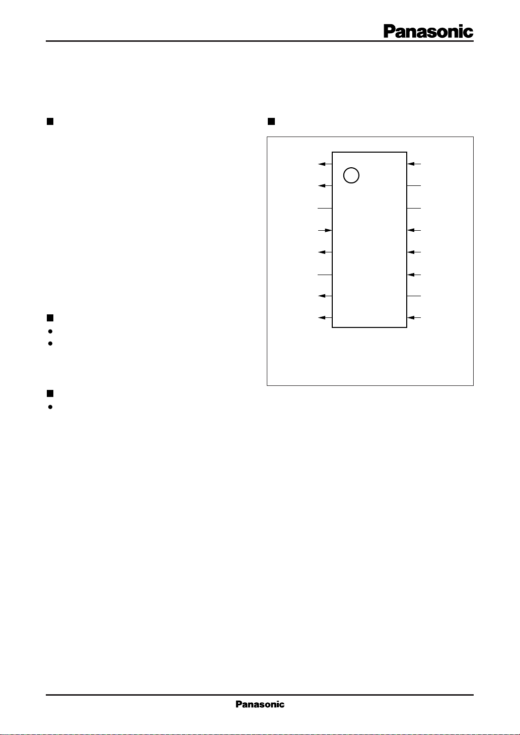
Pin Assignment
VBIASC
VOC
N.C.
V
DD
–V
BB
N.C.
VOY
VBIASY
1
2
3
4
5
6
7
8
SOP016-P-0225
( TOP VIEW )
VINC
16
N.C.
15
N.C.
14
XI
13
V
12
11
10
9
SS
SW
N.C.
VINY
1
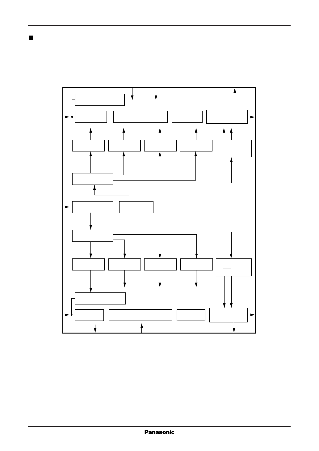
MN3881S CCD Delay Line Series
Block Diagram
VINC
XI
Auto bias circuit
16
Charge input
block
øS driver ø1 driver
Timing adjustment
13
Waveform amplifier
adjustment block
Timing adjustment
SS
V
12
CCD 567 stages
1/2nd frequency
doubler
DD
V
4
Charge
detection block
ø2 driver øR driver
VBIASC
1
Resampling output
amplifier
øSH driver
øSH driver
2
VOC
øS driver ø1 driver
ø2 driver øR driver
øSH driver
øSH driver
Auto clamp circuit
VINY
9
Charge input
block
CCD 566.5 stages
5
BB
–V
11
SW
Charge
detection block
Resampling output
amplifier
8
7
VOY
VBIASY
2
 Loading...