

CCD Delay Line Series
MN3814, MN3814S
NTSC CCD Video Signal Delay Elements
Overview
The MN3814 and MN3814S are 4 fSC CMOS CCD signal
delay elements whose wide bandwidth and low noise make
them ideal for video signal processing applications.
They contain such components as a shift register clock
driver, 906-stage CCD analog shift register, and resampling
output amplifier.
They sample the input using the supplied clock signal with
a frequency of 14.32 MHz, four times the NTSC color signal
subcarrier frequency, and after adding in the attached filter
delay, produce independent delays of 1 H (the horizontal scan
period).
Features
High-precision 1 H delay for video signal
CMOS process for low power consumption
Low EMI levels from clock during driving
Low clock leakage, which allows use of simpler filters
Applications
1 H delays of NTSC video signals, especially for:
Comb filters
Signal-to-noise ratio improvement
Dropout compensation
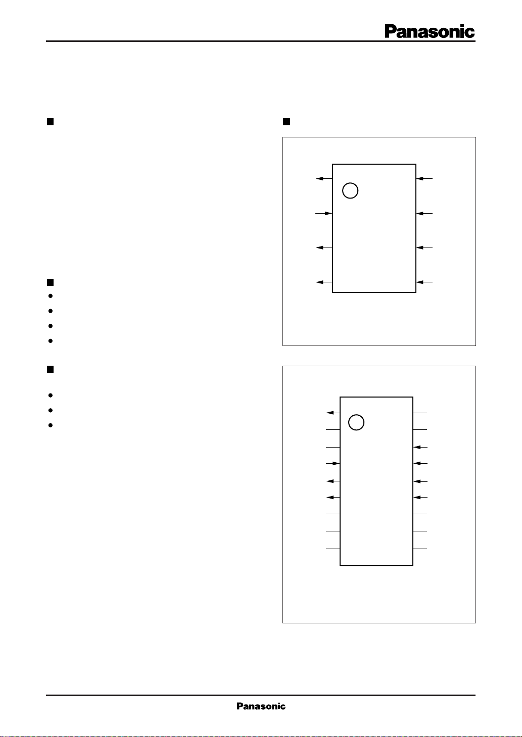
Pin Assignment
MN3814
BB
XI
O
V
N.C.
N.C.
BIAS
N.C.
N.C.
N.C.
BB
X1
V
1
2
3
4
O
V
V
BIAS
V
MN3814S
V
(TOP VIEW)
DIP008-P-300
1
2
3
4
5
6
7
8
9
8
V
DD1
7
V
SS
6
18
17
16
15
14
13
12
11
10
V
DD2
5
V
IN
N.C.
N.C.
V
DD1
V
SS
V
DD2
V
IN
N.C.
N.C.
N.C.
(TOP VIEW)
SOP018-P-0300
1
MN3814, MN3814S CCD Delay Line Series
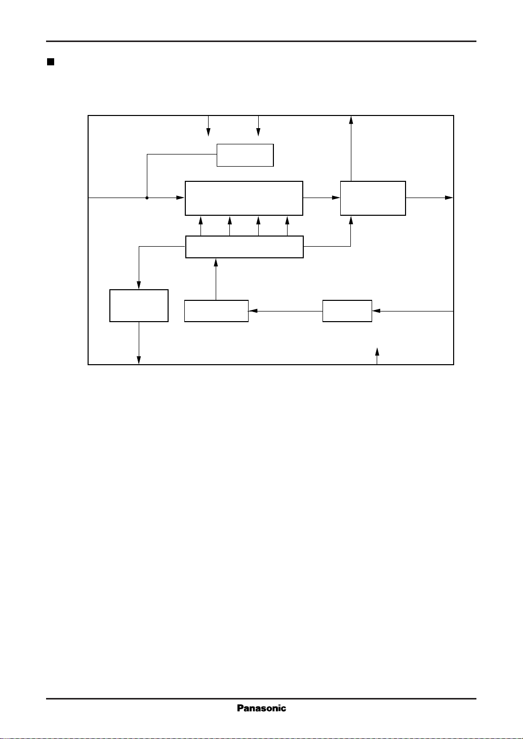
Block Diagram
DD1
V
(16) 8
DD2
V
(14) 6
V
(5) 3
BIAS
Bias circuit
5 (13)
V
IN
906-stage CCD analog shift
register
Resampling
output
amplifier
(6) 4
V
O
øS ø1 ø2 øR øSH
Clock driver
Substrate bias
generator
1 (1)
BB
V
Timing adjustment
Waveform
adjustment
7 (15)
SS
V
(4) 2
XI
The numbers in parentheses are the pin numbers for the MN3814S.
2
 Loading...