

For Audio Equipment
MN35503
D/A Converter for Digital Audio Equipment
Overview
The MN35503 is a CMOS digital-to-analog converter
designed especially for PCM digital audio equipment. It
features a built-in digital filter with 16/20-bit input.
It uses pulse edge modulation (PEM) and JVC advanced
noise shaping (VANS) to yield the high resolution and
low distortion ratio equivalent to those of 20-bit systems
covering the range between 0 and 20 kHz.
The chip incorporating an 8-fold oversampling digital
filter that eliminates a low-pass filter after the D/A
converter and greatly reduces the power consumption of
the overall D/A conversion system.
The chip makes a major contribution to reducing the
cost and size of CD players and other digital audio
equipment.
Features
Built-in 8-fold oversampling digital filter using I2S bus
•Bandwidth ripple: within ±0.05 dB for 0 to 0.454 f
•Cutoff band attenuation (0.546 to 7.454) f
(n–0.03125) f
to (n+0.03125) f
s
n=1 to 7 (integer)
(The above characteristics include those for an
external primary low-pass filter with f
Built-in digital de-emphasis
=32.0 kHz 0 to14.5 kHz max. deviation
f
s
+0.072dB/ – 0.047 dB
fs=44.1 kHz 0 to 20 kHz max. deviation
+0.077dB/ – 0.028 dB
f
=48.0 kHz 0 to 21.8 kHz max. deviation
s
+0.052dB/ – 0.053 dB
(The above characteristics include those for an
external primary low-pass filter with f
The digital filter is designed to deliver the above
bandwidth characteristics when used with an external
primary low-pass filter with f
=1.95 fs.
c
Built-in digital attenuation
Up/down over 32 steps
Support for double-speed operation (192 fs clock)
4PEM output configuration (2PEM output per channel)
Support for low-voltage (3.0 volt) operation
: 37dB
s
: min. 60dB
s
=1.95 fs.)
s
=1.95 fs.)
c
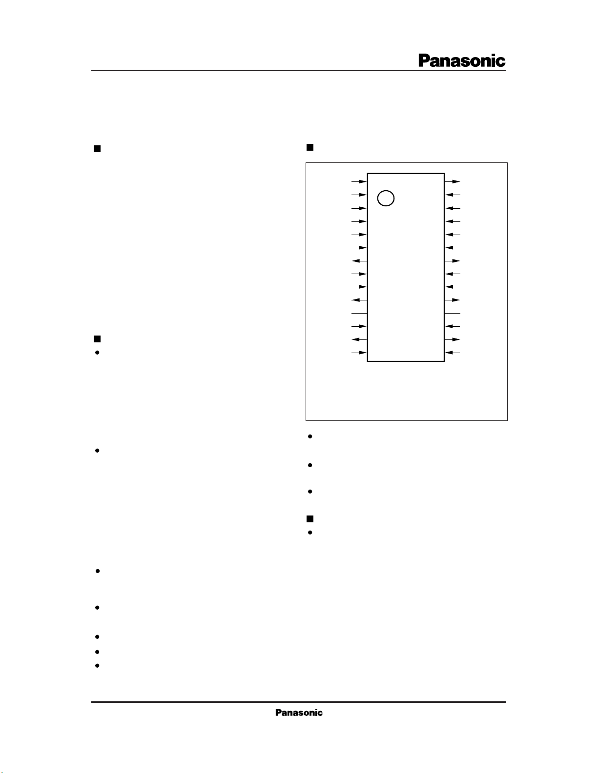
Pin Assignment
, 256f
s
1
2
3
4
5
6
7
8
9
10
11
12
13
14
(TOP VIEW)
SOP028-P-0375
, 384f
, 512fs , 576f
s
s
28
27
26
25
24
23
22
21
20
19
18
17
16
15
MA
DIN
LRCK
BCK
MB
DV
DD2
CKO
DV
SS2
M1
OUT1C
N.C.
AV
DD1
OUT1D
AV
SS1
s
Choice of system clocks:
192f
Choice of input data formats: right-packed or I2S bus
(16 or 20 bits, alternating channel input, MSB first)
Built-in phase comparator
Applications
CD players and other digital audio equipment
PDO
MD
MC
M3
DV
DD1
XIN
XOUT
DV
SS1
M2
OUT2C
N.C.
AV
DD2
OUT2D
AV
SS2
s
MN35503 For Audio Equipment
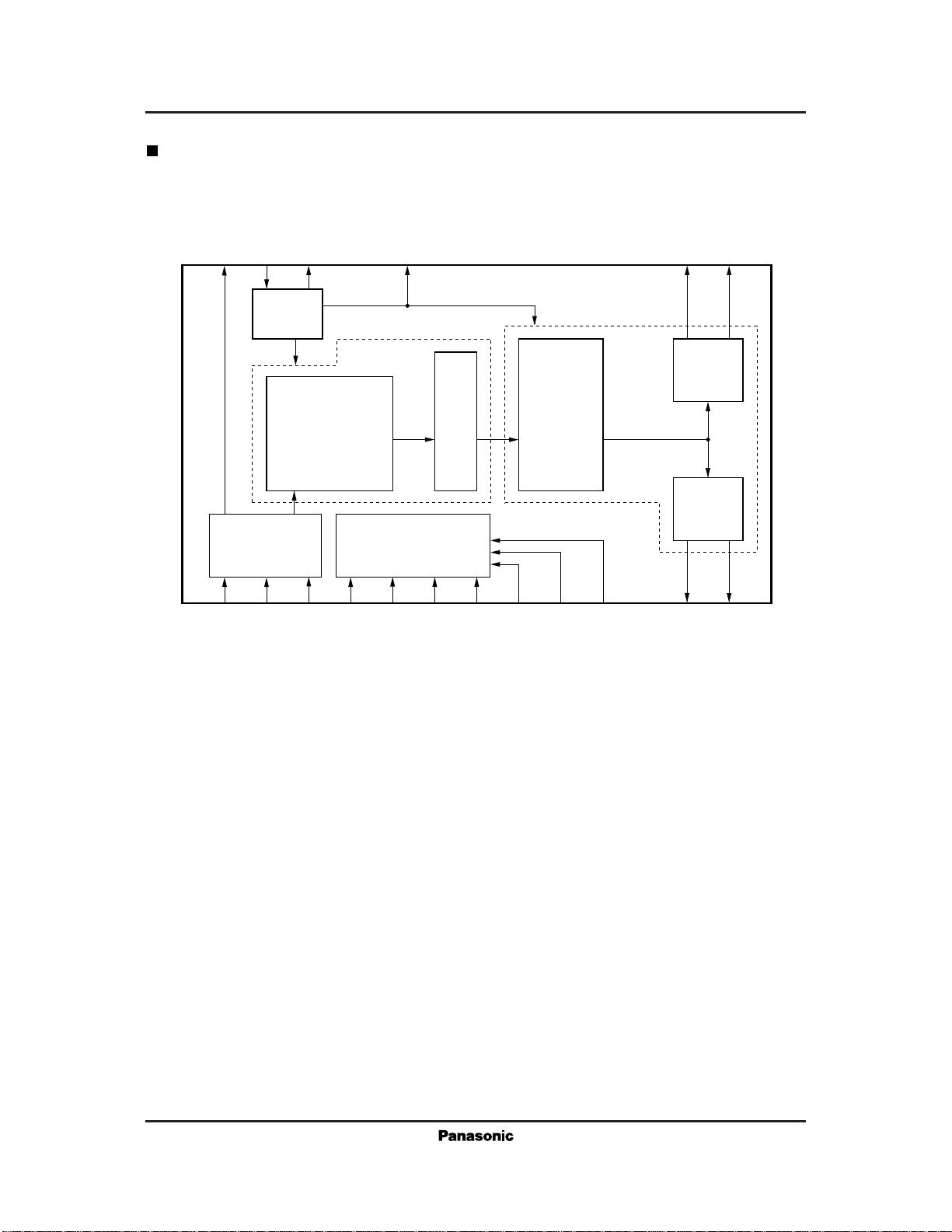
Block Diagram
XIN
PDO
232822
OSC
Block
XOUT
7
CKO
OUT2C
19
OUT2D
16
2
DIN
I/F Block
3
LRCK
DF Block
• 8fs
Over sampling
Digital Filter
• De-emphasis
Filter
• Attenuater
4
9
M1
BCK
1st.
Order
Noise
shaper
Block
Mode Control Block
20
25
M3
M2
PEM
Block
VANS
Block
D/A Block
PEM
Block
1
5
26
MA
MB
MC
27
MD
10
OUT1C
13
OUT1D
For Audio Equipment
MN35503
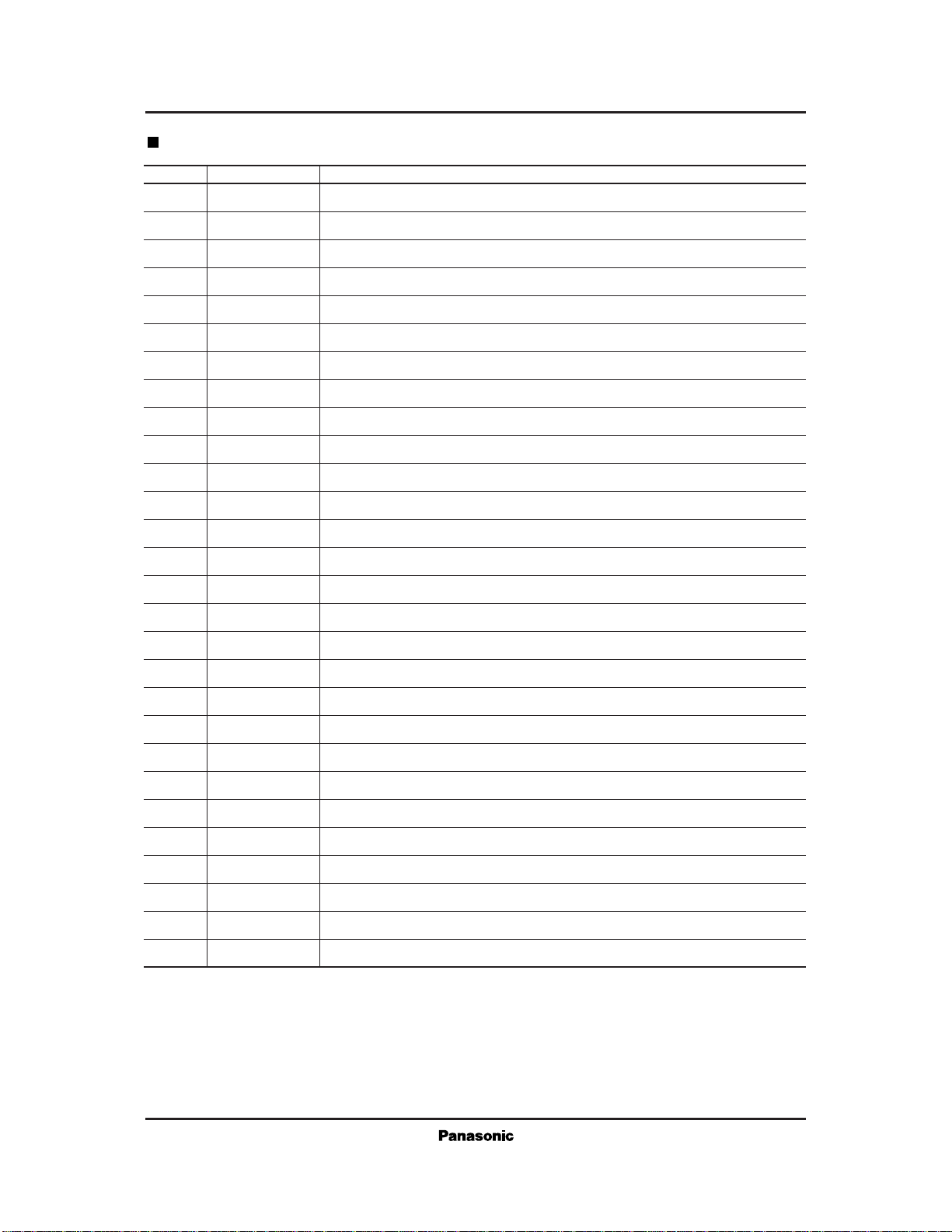
Pin Descriptions
Pin No. Symbol Function Description
1 MA Operating mode selection pin 4 (See Table 1.)
2 DIN Serial data input pin (MSB first)
3 LRCK LR synchronization signal input pin (fs rate)
4 BCK Data shift bit clock input pin
5 MB Operating mode selection pin 5 (See Table 1.)
6DV
DD2
Power supply pin 2 for digital circuits
7 CKO Clock output pin
8DV
SS2
Ground pin 2 for digital circuits
9 M1 Operating mode selection pin 1, with pull-up resistor (See Table 1.)
10 OUT1C PEM output pin 1C (Left channel with reversed phase)
11 N.C. No connection (Leave this pin open.)
12 AV
DD1
Power supply pin 1 for analog circuits
13 OUT1D PEM output pin 1D (Left channel with reversed phase)
14 AV
15 AV
SS1
SS2
Ground pin 1 for analog circuits
Ground pin 2 for analog circuits
16 OUT2D PEM output pin 2D (Right channel with reversed phase)
17 AV
DD2
Power supply pin 2 for analog circuits
18 N.C. No connection (Leave this pin open.)
19 OUT2C PEM output pin 2C (Right channel with reversed phase)
20 M2 Operating mode selection pin 2, with pull-up resistor (See Table 1.)
21 DV
SS1
Ground pin 1 for digital circuits (Ground for oscillator circuit)
22 XOUT Crystal oscillator pin
23 XIN Crystal oscillator pin (external clock input pin) (Built-in feedback resistor)
24 DV
DD1
Power supply pin 1 for digital circuits (for oscillation circuit)
25 M3 Operating mode selection pin 3 (See Table 1.)
26 MC Reset pin/digital attenuation control pin (See Table 1.)
27 MD Reset pin/digital attenuation control pin (See Table 1.)
28 PDO Phase comparator output pin (tristate output)*
Note*1: This pin provides tristate output indicating the result of comparing the phases of the internal fs-rate-signal and the
LRCK input signal. It is at "H" level when the LRCK signal leads and is at "L" level when the signal lags. At all other
times, it is in the high-impedance state.
1
 Loading...