


Panasonic MN35502 Datasheet
For Audio Equipment
MN35502
D/A Converter for Digital Audio Equipment
Overview
The MN35502 is a CMOS digital-to-analog converter
designed especially for PCM digital audio equipment. It
features a built-in digital filter with 16/20-bit input.
It uses pulse edge modulation (PEM) and JVC advanced
noise shaping (VANS) to yield the high resolution and
low distortion ratio equivalent to those of 20-bit systems
covering the range between 0 and 20 kHz.
The chip incorporates an 8-fold oversampling digital
filter that eliminates a low-pass filter after the D/A
converter and thus greatly reduces the power consumption
of the overall D/A conversion system.
Use of single-channel 4PEM output yields a D/A
converter with a low distortion ratio and high signal-tonoise ratio.
The chip makes a major contribution to reducing the
cost and size of CD players and other digital audio
equipment.
Features
Built-in 20-bit, 8-fold oversampling digital filter
• 2-fold oversampling digital filters with 3-stage cascade
configuration
Bandwidth ripple: within ±0.0042 dB for 0 to 0.454 f
Cutoff band attenuation
1±0.454 f
2±0.454 f
4±0.454 f
Transition bandwidth
0.469 f
0.531 f
• Digital filter output: 24 bits
(Output after data compression with primary noise
shaper)
Built-in digital de-emphasis
fs=44.1 kHz 0 to 18kHz max. deviation ±0.055dB
18 to 20kHz max. deviation 0.115dB
Built-in digital attenuation
Up/down over 32 steps
Support for double-speed operation (192 fs clock)
: min. 94.8dB
s
: min. 77.4dB
s
: min. 66.8dB
s
: – 0.12dB
s
: –38dB
s
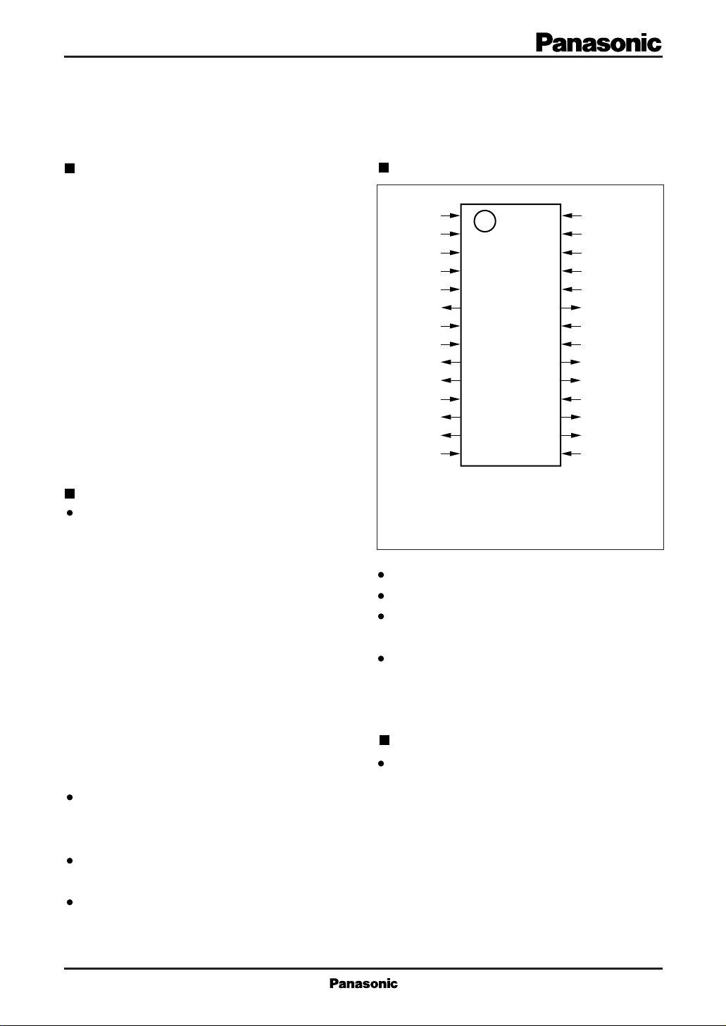
Pin Assignment
DIN
LRCK
BCK
M4
DV
DD2
CKO
DV
SS2
M1
OUT1C
OUT1B
AV
DD1
OUT1D
OUT1A
AV
SS1
s
8PEM output configuration (4PEM output per channel)
Support for low-voltage (3.3-volt) operation
Choice of system clocks:
192 f
Choice of input data formats: left-packed, rightpacked, I
MSB first)
1
2
3
4
5
6
7
8
9
10
11
12
13
14
28
27
26
25
24
23
22
21
20
19
18
17
16
15
(TOP VIEW)
SOP028-P-0375
, 256 fs, 384 fs, 512 fs, 576 f
s
2S
bus (16 or 20 bits, alternating channel input,
s
Applications
CD players and other digital audio equipment
RSBDN
RSBUP
M3
DV
DD1
XIN
XOUT
DV
SS1
M2
OUT2C
OUT2B
AV
DD2
OUT2D
OUT2A
AV
SS2
MN35502 For Audio Equipment
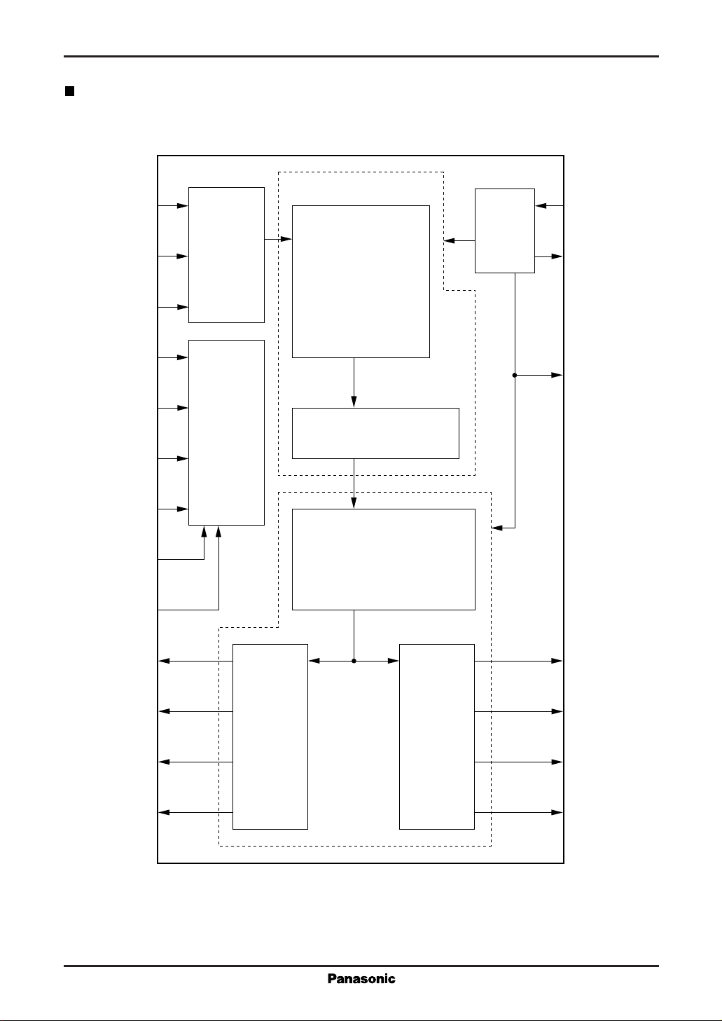
Block Diagram
DIN
LRCK
BCK
M1
M2
M3
M4
RSBDN
1
2
3
8
21
26
4
28
I/F
Block
Mode
Control
Block
DF Block
• De-emphasis
IIR Filter
• Attenuater
• 8fs
Over sampling
Digital Filter
1st. Order
Noise shaper Block
VANS
Noise shaper Block
OSC
Block
24
XIN
23
XOUT
6
CKO
RSBUP
OUT1C
OUT1B
OUT1D
OUT1A
27
9
10
PEM
12
13
Block
D/A Block
PEM
Block
20
OUT2C
19
OUT2B
17
OUT2D
16
OUT2A
For Audio Equipment
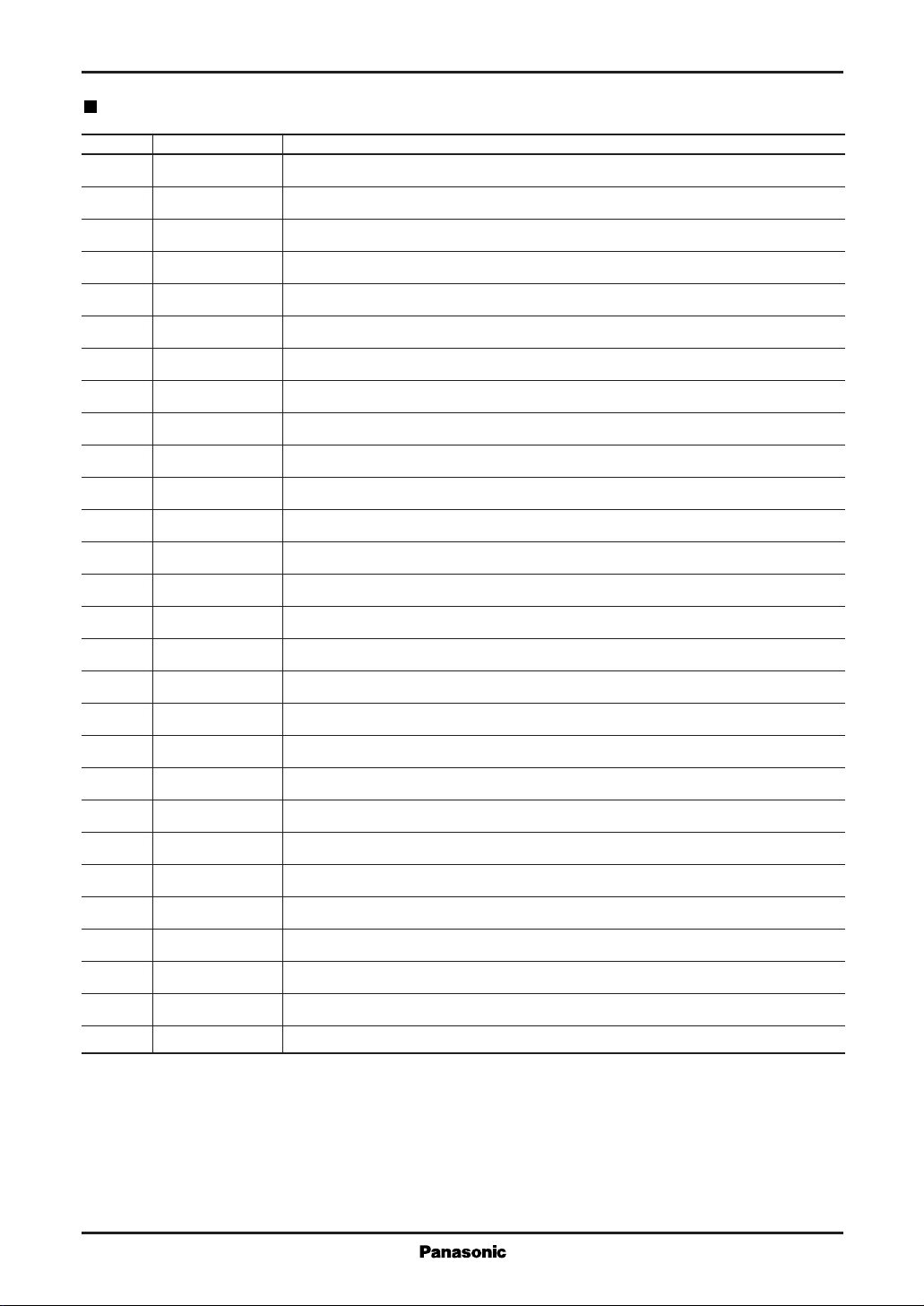
Pin Descriptions
Pin No. Pin Name Function Description
1 DIN Serial data pin (MSB first)
2 LRCK LR synchronization signal input pin (fs rate)
3 BCK Data shift bit clock input pin
4 M4 Operating mode selection pin 4 (See Table 1.)
MN35502
5DV
DD2
Power supply pin 2 for digital circuits
6 CKO Clock output pin
7DV
SS2
Ground pin for digital circuits
8 M1 Operating mode selection pin 1, with pull-up resistor (See Table 1.)
9 OUT1C PEM output pin 1C (Left channel with reversed phase)
10 OUT1B PEM output pin 1B (Left channel with same phase)
11 AV
DD1
Power supply pin 1 for analog circuits
12 OUT1D PEM output pin 1D (Left channel with reversed phase)
13 OUT1A PEM output pin 1A (Left channel with same phase)
14 AV
15 AV
SS1
SS2
Ground pin 1 for analog circuits
Ground pin 2 for analog circuits
16 OUT2A PEM output pin 2A (Right channel with same phase)
17 OUT2D PEM output pin 2D (Right channel with reversed phase)
18 AV
DD2
Power supply pin 2 for analog circuits
19 OUT2B PEM output pin 2B (Right channel with same phase)
20 OUT2C PEM output pin 2C (Right channel with reversed phase)
21 M2 Operating mode selection pin 2, with pull-up resistor (See Table 1.)
22 DV
SS1
Ground pin 1 for digital circuits (Ground for oscillator circuit)
23 XOUT Crystal oscillator pin
24 XIN Crystal oscillator pin (external clock input pin) (Built-in feedback resistor)
25 DV
DD1
Power supply pin 1 for digital circuits
26 M3 Operating mode selection pin 3, with pull-up resistor (See Table 1.)
27 RSBUP Reset pin/digital attenuation control pin (See Table 2.)
28 RSBDN Reset pin/digital attenuation control pin (See Table 2.)