

Panasonic MN3114 Datasheet
Video Camera IC
MN3114
Vertical Driver (8 channels) for CCD Area Image Sensors
■ Overview
The MN3114 is an 8-channel vertical driver for twodimensional interline CCD area image sensors that also
integrates a single SUB driver channel on the same chip.
Adoption of this IC can reduce both power consumption and parts counts in end products.
■ Features
•
Vertical driver block:
Consists of level shifters and 2-value/3-value output
driver circuits.
•
SUB driver block:
Consists of a level shifter and a 2-value output driver
circuit.
•
Package: 24-pin SSOP
■ Applications
•
Digital still cameras, video cameras
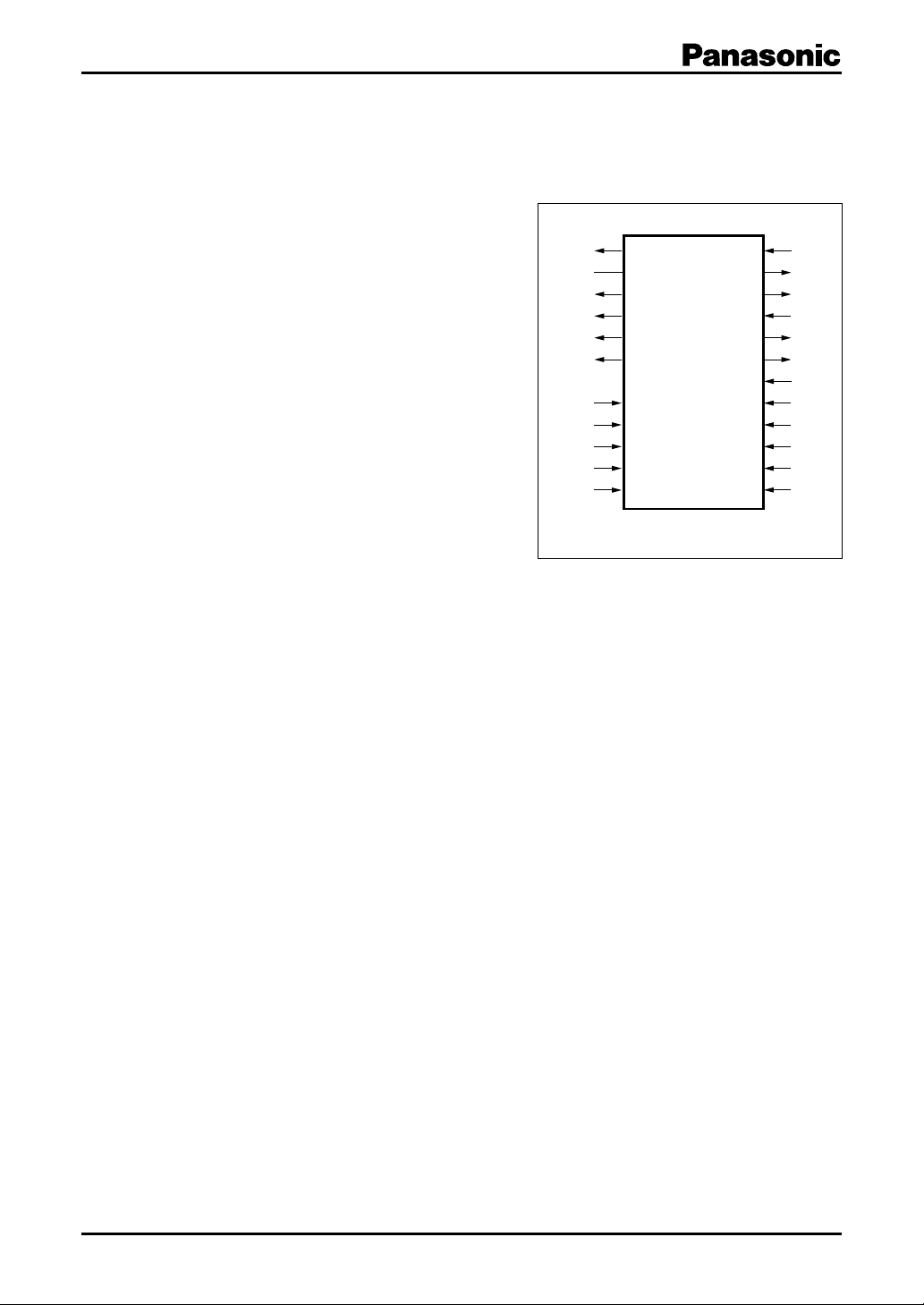
OSUB
VL
OV8
OV4
OV1
OV5
(N.C.)
VDC
CH3
IV1
CH1
IV4
1
2
3
4
5
6
7
8
9
10
11
12
(TOP VIEW)
24
23
22
21
20
19
18
17
16
15
14
13
VHH
OV6
OV2
VM
OV3
OV7
VH
CH4
IV3
CH2
IV2
ISUB
Preliminary
Publication date: April 2002 SDB00057AEM
1
MN3114 Video Camera IC
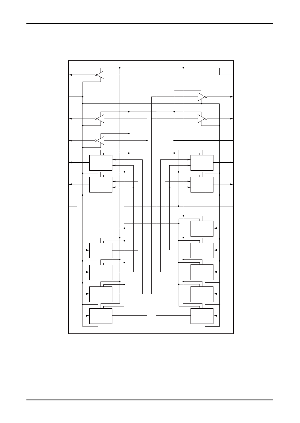
■ Block Diagram
OSUB
VL
OV8
OV4
OV1
OV5
N.C.
VDC
1
2
3
4
5
6
7
8
3-value
driver
3-value
driver
3-value
driver
3-value
driver
Level
shifter
24
23
22
21
20
19
18
17
VHH
OV6
OV2
VM
OV3
OV7
VH
CH4
CH3
IV1
CH1
9
10
11
Level
shifter
Level
shifter
Level
shifter
Preliminary
12
IV4
Note) VDC, VL, and VM: Common power supply
VHH and VH: SUB driver block and vertical driver 3-value independent power supply
2
Level
shifter
SDB00057AEM
Level
shifter
Level
shifter
Level
shifter
Level
shifter
16
15
14
13
IV3
CH2
IV2
ISUB
Video Camera IC MN3114
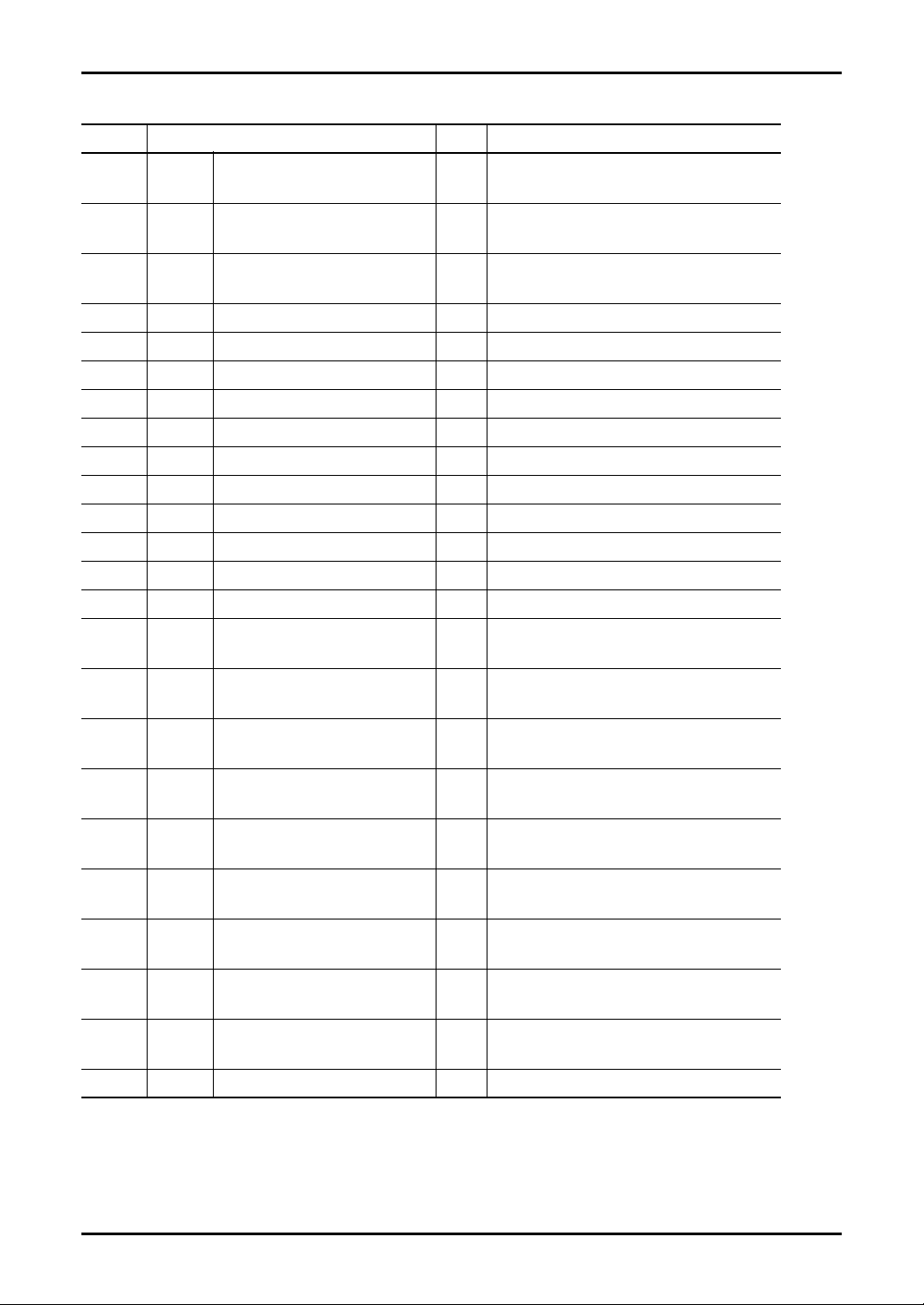
■ Pin Descriptions
Pin No. Pin name I/O Description
8 VDC Input block I Low-voltage system high-level input
high-level supply voltage
18 VH Vertical driver block I High-voltage system high-level input
high-level supply voltage
24 VHH SUB driver block I High-voltage system high-level input
high-level supply voltage
21 VM Middle-level supply voltage I High-voltage system middle-level input
2 VL Low-level supply voltage I High-voltage system low-level input
10 IV1 Transfer pulse input I Charge transfer pulse input
14 IV2 Transfer pulse input I Charge transfer pulse input
16 IV3 Transfer pulse input I Charge transfer pulse input
12 IV4 Transfer pulse input I Charge transfer pulse input
11 CH1 Charge pulse input I Charge readout pulse input
15 CH2 Charge pulse input I Charge readout pulse input
9 CH3 Charge pulse input I Charge readout pulse input
17 CH4 Charge pulse input I Charge readout pulse input
13 ISUB SUB pulse input I Unneeded charge sweep-out pulse input
5 OV1 3-value transfer pulse O 3-value transfer pulse output
output (VH, VM, or VL)
22 OV2 2-value transfer pulse O 2-value transfer pulse output
output (VH or VL)
20 OV3 3-value transfer pulse O 3-value transfer pulse output
output (VH, VM, or VL)
4 OV4 2-value transfer pulse O 2-value transfer pulse output
output (VH or VL)
6 OV5 3-value transfer pulse O 3-value transfer pulse output
output (VH, VM, or VL)
23 OV6 2-value transfer pulse O 2-value transfer pulse output
output (VH or VL)
19 OV7 3-value transfer pulse O 3-value transfer pulse output
3 OV8 2-value transfer pulse O 2-value transfer pulse output
1 OSUB SUB pulse output O Unneeded charge sweep-out pulse output
7 N.C.
Preliminary
output (VH, VM, or VL)
output (VH or VL)
(VHH or VL)
SDB00057AEM
3
MN3114 Video Camera IC
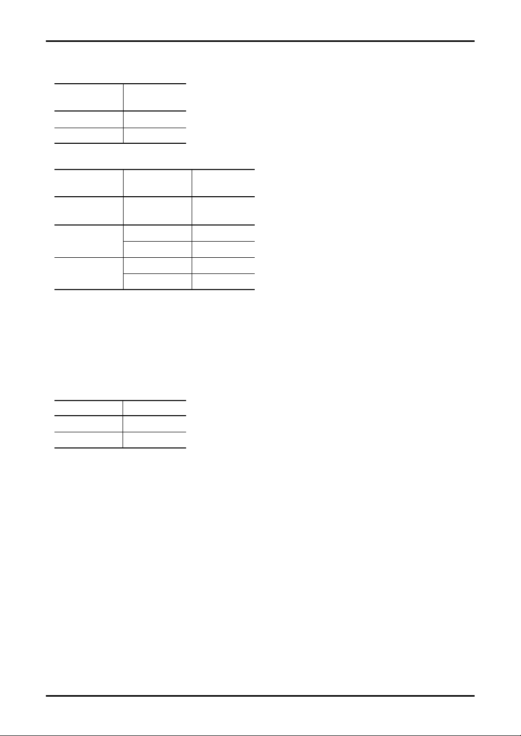
■ Operating Mode Table
1. 2-value transfer pulse (vertical driver block)
IV2 OV2, OV6
IV4 OV4, OV8
High Low
Low Mid
2. 3-value transfer pulse
CH1 IV1 OV1
CH2 IV3 OV3
CH3 IV1 OV5
CH4 IV3 OV7
High High Low
Low Mid
Low High Low
Low High
Note) IV1, IV2, IV3, IV4, CH1, CH2
High: VDC
Low: GND
OV1, OV2, OV3, OV4, OV5, OV6, OV7, OV8
High: VH
Mid: VM
Low: VL
3. Unneeded charge sweep-out pulse (SUB driver block)
ISUB OSUB
High Low
Low High
Note) ISUB
High: VDC
Low: GND
OSUB
High: VHH
Low: VL
Preliminary
4
SDB00057AEM
 Loading...