

Panasonic MN3112SA Datasheet
For Video Equipment
MN3112SA
Vertical Driver for Video-Camera CCD Area-Image-Sensor
Overview
The MN3112SA is a vertical driver LSI incorporating
four vertical driver channels and one sub driver channel
for a 2-dimensional interline CCD image sensor.
The MN3112SA enables low current dissipation and
the part reductions.
Features
3V power supply for input section
Applications
Video cameras
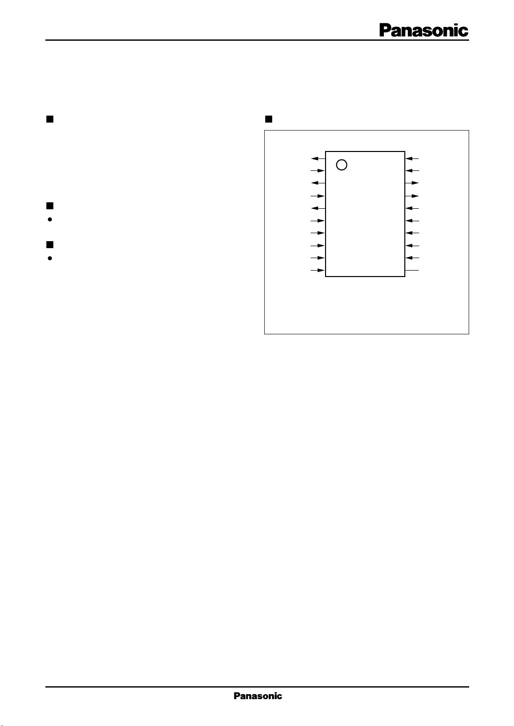
Pin Assignment
OSUB
V
OV2
V
M13
OV1
V
DC
IV1
CH1
IV2
ISUB
1
2
L
3
4
5
6
7
8
9
10
SSOP020-P-0225
(TOP VIEW)
20
19
18
17
16
15
14
13
12
11
V
HH
V
M24
OV4
OV3
V
H
GND
IV3
CH2
IV4
N.C.
MN3112SA For Video Equipment
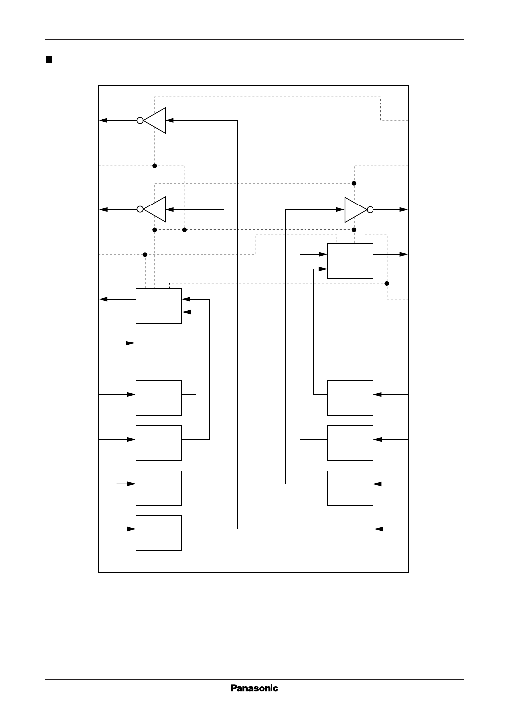
Block Diagram
OSUB
V
OV2
V
M13
OV1
V
DC
IV1
1
2
L
3
20
19
18
V
HH
V
M24
OV4
4
Tristate
17
OV3
driver
5
Tristate
16
V
H
driver
6
15
GND
7
Level
conversion
Level
conversion
14
IV3
CH1
IV2
ISUB
8
Level
conversion
9
Level
conversion
10
Level
conversion
V
, VL , GND : Common power supply
DC
V
, V
M13
V
, V
HH
: Binary and tristate independent power supplies for vertical driver section
M24
: Independent power supplies for sub driver section and vertical driver section
H
Level
conversion
Level
conversion
13
12
11
CH2
IV4
N.C.
For Video Equipment MN3112SA
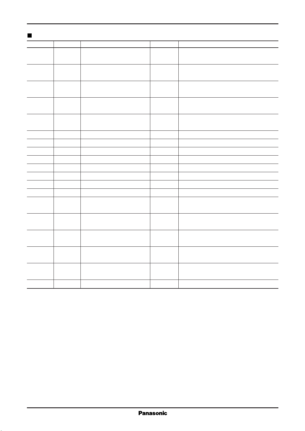
Pin Descriptions
Pin No. Symbol Pin Name I/O Function Description
6V
DC
15 GND Input section low-level
16 V
20 V
4V
19 V
2V
H
HH
M13
M24
L
9 IV2 Transfer pulse input I Charge transfer pulse input pin
12 IV4 Transfer pulse input I Charge transfer pulse input pin
7 IV1 Transfer pulse input I Charge transfer pulse input pin
14 IV3 Transfer pulse input I Charge transfer pulse input pin
8 CH1 Charge pulse input I Charge read pulse input pin
13 CH1 Charge pulse input I Charge read pulse input pin
10 ISUB SUB pulse input I Unwanted charge sourcing pulse input pin
18 OV4 Binary transfer pulse O Binary transfer pulse output pin
3 OV2 Binary transfer pulse O Binary transfer pulse output pin
17 OV3 Tristate transfer pulse O Tristate transfer pulse output pin
5 OV1 Tristate transfer pulse O Tristate transfer pulse output pin
1 OSUB SUB pulse output O Unwanted charge sourcing pulse output pin
11 N.C. No connection —
Input section high-level
power supply
power supply
Vertical driver section
high-level power supply
SUB driver section
high-level power supply
Middle-level power supply I
I 5V high-level input
I 5V low-level input
I High-level input at high-voltage section
I High-level input at high-voltage section
Middle-level input at high-voltage section
Input externally to both V
M13
and V
M24
Low-level power supply I Low-level input at high-voltage section
output (V
output (V
output (VH , V
output (VH , V
(V
M24
M24
HH
, VL)
, VL)
M13
M13
, VL)
, VL)
, VL)
.
 Loading...