

Panasonic MN31121SA User Manual
Video Camera LSI
MN31121SA
CCD Image Sensor Vertical Driver IC
■ Overview
The MN31121SA is a 2D interline CCD image sensor
vertical driver IC that integrates four vertical driver channels and one SUB drive channel on a single chip. This IC
can reduce power consumption and the number of external parts.
The MN31121SA consists of a vertical driver block
that includes both level shifter circuits and 2-value and
3-value output driver circuits, and a SUB driver block that
includes level shifter and 2-value output driver circuits.
■ Features
•
Level shifter circuits
Input (V
•
2-value output driver circuits (vertical driver block)
Outputs: V
•
3-value output driver circuits (vertical driver block)
Outputs: V
•
2-value output driver circuits (SUB driver block)
Outputs: V
, ground) → output (VHH , VL)
DC
and V
M24
H
HH
, V
M13
and V
L
, and V
L
L
O
O
V
O
V
CH1
I
SUB
V
V2
M13
V1
DC
I
V1
I
V2
SUB
1
2
L
3
4
5
6
7
8
9
10
(TOP VIEW)
20
19
18
17
16
15
14
13
12
11
V
HH
V
M24
O
V4
O
V3
V
H
N.C.
I
V3
CH2
I
V4
N.C.
■ Applications
•
Video cameras, surveillance cameras, digital still cam-
eras, CCD camera systems
Publication date: April 2003 SDB00054CEM
1
MN31121SA
■ Block Diagram
1
O
SUB
2
V
L
3
O
V2
4
V
M13
5
O
V1
6
V
DC
7
I
V1
3-value
driver
Level
shifter
3-value
driver
Level
shifter
20
19
18
17
16
15
14
V
HH
V
M24
O
V4
O
V3
V
H
N.C.
I
V3
8
CH1
9
I
V2
10
I
SUB
Note) VDC , VL: Common power supply
V
, V
M13
VHH , VH: SUB driver block and vertical driver block 3-value independent power supply
: Vertical driver block 2-value and 3-value independent power supply
M24
2
Level
shifter
Level
shifter
Level
shifter
SDB00054CEM
Level
shifter
Level
shifter
13
12
11
CH2
I
V4
N.C.
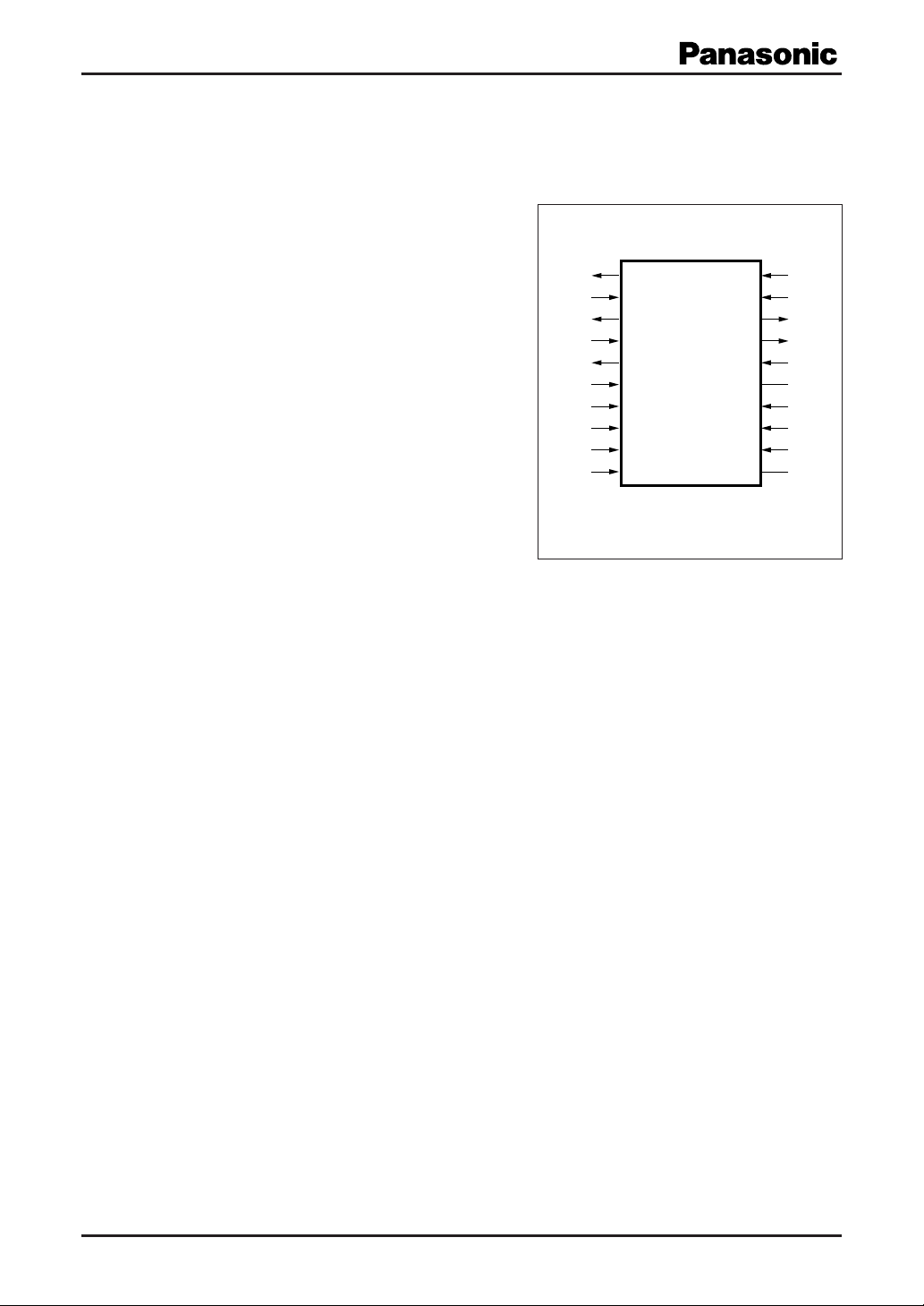
■ Pin Descriptions
Pin No. Pin name I/O Description
1O
SUB
2VLI Low-level power supply
3OV2O 2-value transfer pulse output
4V
M13
5OV1O 3-value transfer pulse output
6VDCI Input block high-level power supply
7IV1I Transfer pulse input
8 CH1 I Charge pulse input
9IV2I Transfer pulse input
10 I
SUB
11 N.C. Unused
12 I
V4
13 CH2 I Charge pulse input
14 I
V3
15 N.C. Unused
16 V
17 O
18 O
19 V
20 V
H
V3
V4
M24
HH
O SUB pulse output
I Mid-level power supply
I SUB pulse input
I Transfer pulse input
I Transfer pulse input
I High-level power supply of vertical driver block
O 3-value transfer pulse output
O 2-value transfer pulse output
I Mid-level power supply
I High-level power supply of SUB driver block
MN31121SA
■ Electrical Characteristics
1. Absolute Maximum Ratings
Parameter Symbol Rating Unit
Supply voltage 1 VHH-V
Supply voltage 2 VH-V
Supply voltage 3 V
Supply voltage 4 V
Negative supply voltage V
Input voltage V
Input and output clamp diode currents IIC , I
Maximum DC load current I
Maximum load capacitance C
Power dissipation P
Operating temperature T
Storage temperature T
Note) The absolute maximum ratings are stress ratings only, and do not guarantee operation. Stress in excess of the maximum rating
may destroy the device.
L
, V
M13
DC
L
I
OC
ODC
L
D
opr
stg
SDB00054CEM
L
M24
VL− 0.3 to VDC+0.3 V
32 V
30 V
VL to 6 V
0 to 7 V
−12 to 0 V
±10 mA
±3mA
5 500 pF/PIN
180 mW
−10 to +70 °C
−50 to +125 °C
3
MN31121SA
■ Electrical Characteristics (continued)
2. Operating Conditions at Ta = −10°C to +70°C
Parameter Symbol Conditions Min Typ Max Unit
Supply voltage 1 VHH-V
Supply voltage 2 VH-V
Supply voltage 3
V
Supply voltage 4 V
Supply voltage 5 V
Negative supply voltage V
Input frequency f
, V
M13
HH-VM13
VHH-V
IN
L
L
M24
M24
DC
L
VH-VL 30.5 V
17 28 V
−1 4V
12 V
2.5 3.6 V
−10 −4V
20 kHz
3. DC Characteristics at
VHH = 18.0 V, VH = 13.0 V, V
Parameter Symbol Conditions Min Typ Max Unit
Quiescent supply current I
Operating supply current I
DDST
DDDYN
Input Pins IV1 , IV2 , IV3 , IV4 , CH1, CH2, I
High-level voltage V
Low-level voltage V
High-level voltage V
Low-level voltage V
Input leakage current I
IH
IL
IH
IL
ILK
Output Pins 1 (2-value outputs) OV2 , O
Mid-level output voltage V
Low-level output voltage V
Output on resistance (mid level) R
Output on resistance (low level) R
OM1
OL1
ONM1IOM1
ONL1
Output Pins 2 (3-value outputs) OV1 , O
High-level output voltage V
Mid-level output voltage V
Low-level output voltage V
Output on resistance (high level) R
Output on resistance (mid level) R
Output on resistance (low level) R
Output Pins 3 (SUB outputs) O
High-level output voltage V
Low-level output voltage V
OH2
OM2
OL2
ONH2
ONM2IOM2
ONL2
SUB
OHH3
OL3
= V
M13
= 1.0 V, VL = −7.0 V, VDC = 3.00 V, Ta = −10°C to +70°C
M24
VI = GND, VDC = 2.6 V 2mA
VI = GND, VDC = 3.0 V 5
Refer to test conditions 7mA
(Input pulse timing, output load circuit)
VI = GND, V
SUB
VDC = 2.6 V 1.75 V
DC
DC
V
0.0 0.15 V
VDC = 3.0 V 2.5 V
DC
V
0.0 0.3 V
VI = 0 V to V
V4
I
= −1 mA 0.9 V
OM1
I
= 1 mA V
OL1
DC
−1.0 +1.0 µA
V
−6.9 V
L
M24
= −50 mA 60 Ω
I
= 50 mA 40 Ω
OL1
V3
I
= −1 mA 12.9 V
OH2
I
= −1 mA 0.9 V
OM2
I
= 1 mA V
OL2
I
= −50 mA 70 Ω
OH2
−6.9 V
L
M13
V
H
V
= ±50 mA 60 Ω
I
= 50 mA 60 Ω
OL2
I
= −1 mA 17.9 V
OHH3
I
= 1 mA V
OL3
L
−6.9 V
HH
V
4
SDB00054CEM
 Loading...