

Panasonic MN3111H Datasheet
For Video Equipment
MN3111H
Vertical Driver LSI for Video Camera CCD Area Image Sensor
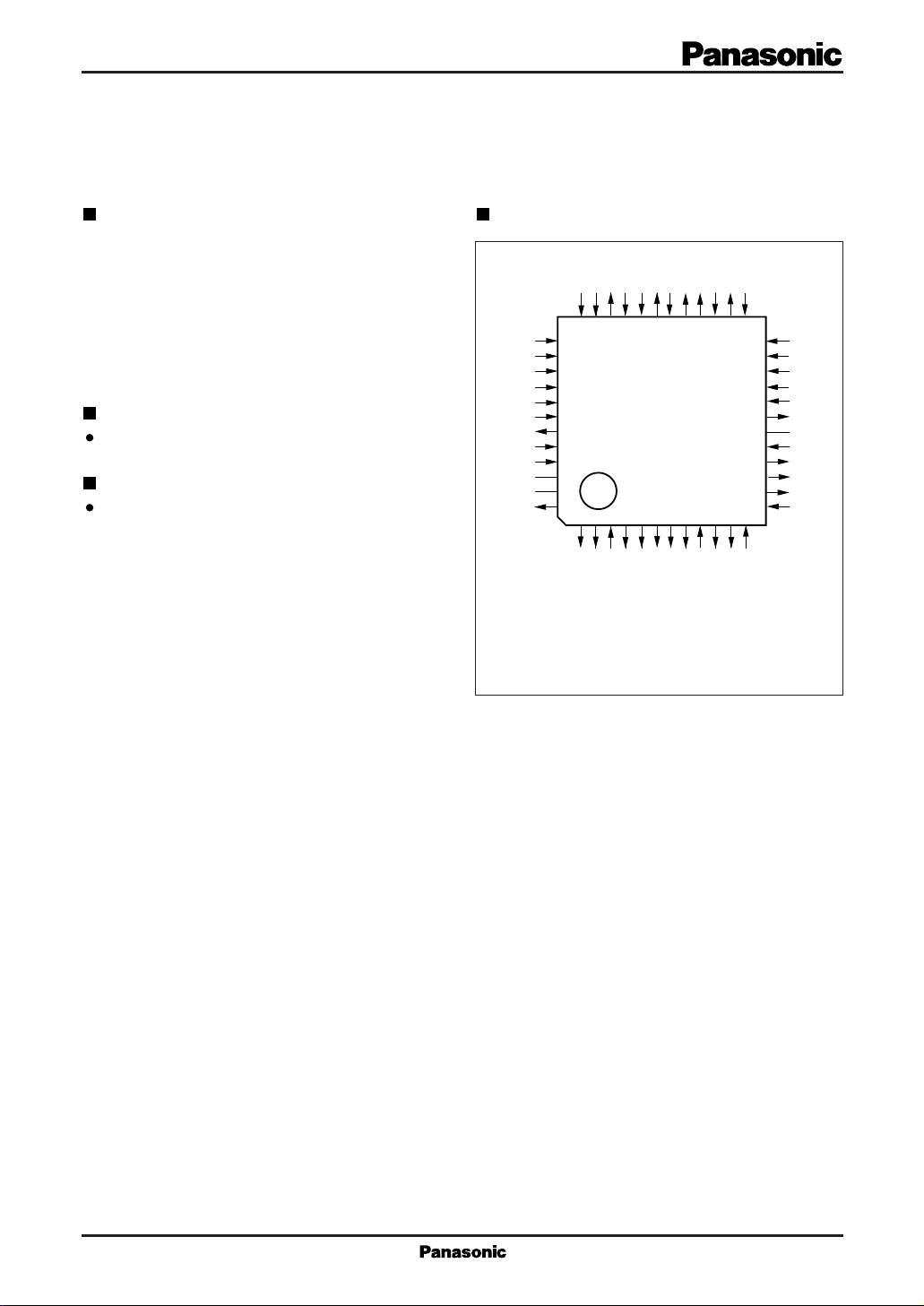
Pin Assignment Overview
The MN3111H is a vertical driver LSI for a two-dimensional interline CCD image sensor. It features a built-in
power supply circuit that, in conjunction with such
external components as four booster capacitors, six voltage stabilization capacitors, eight Schottky barrier diodes,
and two Zener diodes, produces stabilized +15.0V and
–10.0V power supplies from a +5.0V input and HD pulses.
Features
Single 5 volt power supply
Applications
Video cameras
ISUB
CH1
IV1
IV3
CH2
SENSE2
V
OUT–
V
IN –
GND
N.C.
N.C.
C4 –
EEVHH
V
OSUB
3635343332313029282726
37
38
39
40
41
42
43
44
45
46
47
48
1234567891011
VL2VL1OV1
V
M13
OV3
OV2
V
M24
OV4
V
25
24
23
22
21
20
19
18
17
16
15
14
13
12
H
V
DD
V
CC2
IV2
IV4
SENSE1
V
OUT+
N.C.
V
IN+
CAP3
CAP2
CAP1
TEST
EE
C2–
C3+
C3 –
GND
OV
(TOP VIEW)
QFH048-P-0707
C2+
C1+
C1–
DD
CC1
HD
C4+
V
OV
MN3111H For Video Equipment
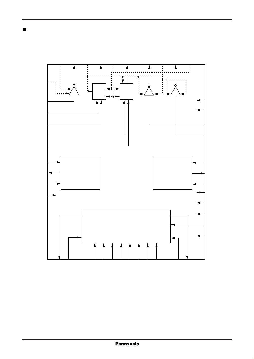
Block Diagram
VL2
V
ISUB
IV1
CH1
IV3
CH2
SENSE2
V
OUT–
V
IN –
GND
HH
V
34
35
OSUB31V
32
L1
OV129V
30
M13
OV3
28
OV2
M24
V
27
26
OV4
H
V
25
33
36
EE
Tristate
driver
37
39
38
40
Tristate
driver
24
V
DD
23
V
CC2
22
IV2
21
IV4
41
42
43
Negative voltage
monitor
Positive voltage
monitor
44
45
Negative and positive boosting voltage generator
20
19
17
16
15
14
12
13
SENSE1
V
OUT+
V
IN+
CAP3
CAP2
CAP1
HD
TEST
3
1
EE
GND
OV
8
C1–
7
C1+
4
6
5
2
48
10
C2–
C2+
C3 –
C3+
C4 –
C4+
9
11
DD
CC1
V
OV
For Video Equipment MN3111H
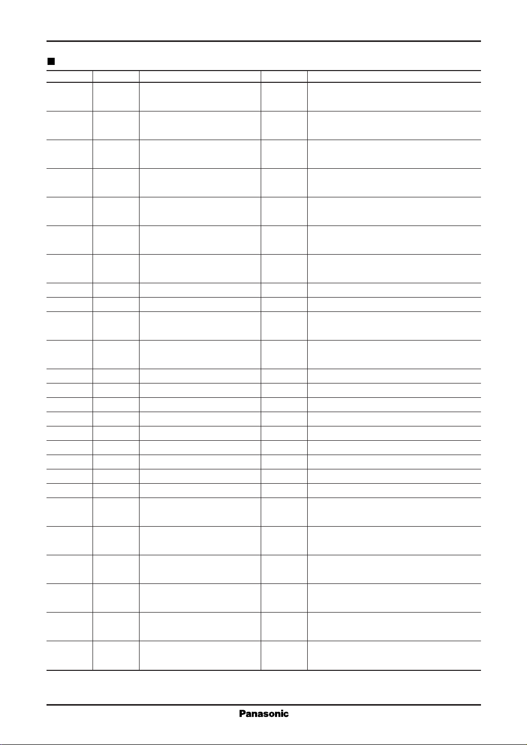
Pin Descriptions
Pin No. Symbol Pin Name I/O Function Description
9V
23 V
CC1
CC2
3 GND "L" level power supply I "L" level input for 5 volt circuits
45 for input block
25 V
35 V
30 V
27 V
32 V
33 V
24 V
36 V
17 V
44 V
H
HH
M13
M24
L1
L2
DD
EE
IN+
IN –
13 TEST Test input I Test pin (Keep this pin at "H" level.)
12 HD HD pulse input I HD pulse input pin
22 IV2 Transfer pulse input I Charge transfer pulse input pin
21 IV4 Transfer pulse input I Charge transfer pulse input pin
39 IV1 Transfer pulse input I Charge transfer pulse input pin
40 IV3 Transfer pulse input I Charge transfer pulse input pin
38 CH1 Charge pulse input I Charge readout pulse input pin
41 CH2 Charge pulse input I Charge readout pulse input pin
37 ISUB SUB pulse input I Unwanted charge rejection pulse input pin
20 SENSE1 Positive voltage monitor I Positive voltage monitor control sensing
42 SENSE2 Negative voltage monitor I Negative voltage monitor control sensing
7 C1+ C1 connection O Booster block voltage charging capacitor
8 C1– connection pins
6 C2+ C2 connection O Booster block voltage charging capacitor
4 C2– connection pins
2 C3+ C3 connection O Booster block voltage charging capacitor
5 C3 – connection pins
10 C4+ C4 connection O Booster block voltage charging capacitor
48 C4 – connection pins
"H" level power supply I "H" level input for 5 volt circuits
for input block
"H" level power supply I "H" level input for high-voltage circuits
for vertical driver
"H" level power supply I "H" level input for high-voltage circuits
for SUB driver
"M" level power supply I "M" level input for high-voltage circuits
for vertical driver
"L" level power supply I "L" level input for high-voltage circuits
for vertical driver
"L" level power supply I "L" level input for high-voltage circuits
for SUB driver
Driver power supply 1 I "H" level for high-voltage circuits
Driver power supply 2 I "L" level for high-voltage circuits
Voltage input for positive I Voltage input pin for positive voltage
voltage monitor monitor
Voltage input for negative I Voltage input pin for negative voltage
voltage monitor monitor
sensing input pin (Leave this pin open.)
sensing input pin (Leave this pin open.)
MN3111H For Video Equipment
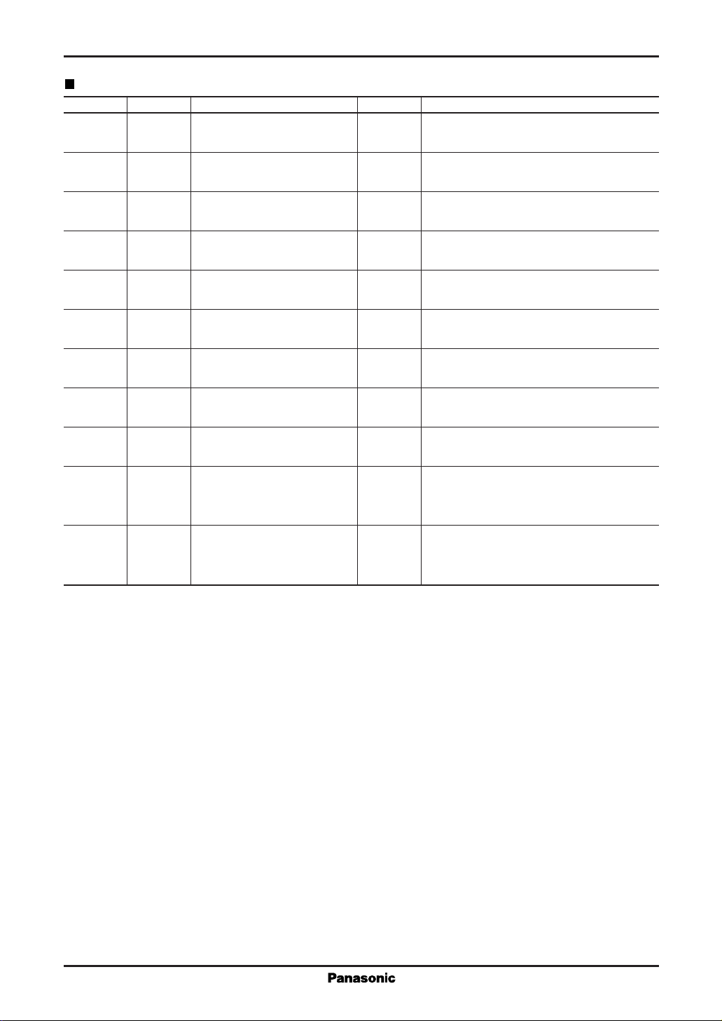
Pin Descriptions (continued)
Pin No. Symbol Pin Name I/O Function Description
11 OV
1OV
19 V
43 V
DD
EE
OUT+
OUT-
26 OV4 Binary transfer pulse O Binary (V
28 OV2 Binary transfer pulse O Binary (V
29 OV3 Tristate transfer pulse O Tristate (V
31 OV1 Tristate transfer pulse O Tristate (V
34 OSUB SUB pulse output O Unwanted charge (V
14 CAP1 Stabilizing capacitor O Pins for connecting capacitors for internal
15 CAP2 connection voltage stabilization circuits
16 CAP3
18 N.C. No connection —
46
47
Booster block positive O Booster block positive voltage
voltage output output pin
Booster block negative O Booster block negative voltage
voltage output output pin
Positive regulated voltage O Positive voltage monitor output pin
output (Leave this pin open.)
Negative regulated voltage O Negative voltage monitor output pin
output (Leave this pin open.)
, VL1) transfer pulse
M24
output output pin
, VL1) transfer pulse
M24
output output pin
, V
H
, VL1) transfer pulse
M13
output output pin
, V
H
, VL1) transfer pulse
M13
output output pin
, VL2) rejection
HH
pulse input pin
 Loading...