

Panasonic MN12511 Datasheet
Microcontroller Peripheral LSIs
MN12511
Fluorescent Display Tube Driver LSI
■ Overview
The MN12511 is a fluorescent display tube driver LSI. It
accepts data for display transferred over a serial interface,
generates the digit and/or segment drive signals, and outputs those signals from 16 high-voltage ports.
This LSI allows the number of digits displayed to be
increased easily by the cascade connection of additional
MN12511 LSIs. Also, the MN12511 does not preassign
the outputs to digits or segments, so it can be used with a
wide range of display types.
■ Features
•
Sixteen high-voltage handling output ports
Number of digit outputs (DGT): 1 to 15 outputs can be
arbitrarily assigned
Number of segment outputs (SEG): 1 to 15 outputs can
be arbitrarily assigned
•
FLP display
• The display mode can be set to any combination of
from 1 DGT × 15 SEG to 15 DGT × 1 SEG
• The display on/off state can be controlled from the
OE pin.
•
Four-wire serial interface (Includes a chip select signal)
• Built-in shift register
• The MN12511 can be connected in cascade.
•
Supply voltage
Digital block (V
High-voltage (V
): + 4.5 to 5.5 V
DD
): VDD − 35 V
pp
V
NCE
OE
NSDO
NSDI
NSCK
V
V
DD
D15
D14
D13
D12
PP
SS
1
2
3
4
5
6
7
8
9
10
11
12
(TOP VIEW)
24
23
22
21
20
19
18
17
16
15
14
13
D0
D1
D2
D3
D4
D5
D6
D7
D8
D9
D10
D11
■ Applications
•
Video, audio, and other equipment that uses fluorescent
display tubes
1
MN12511 Microcontroller Peripheral LSIs
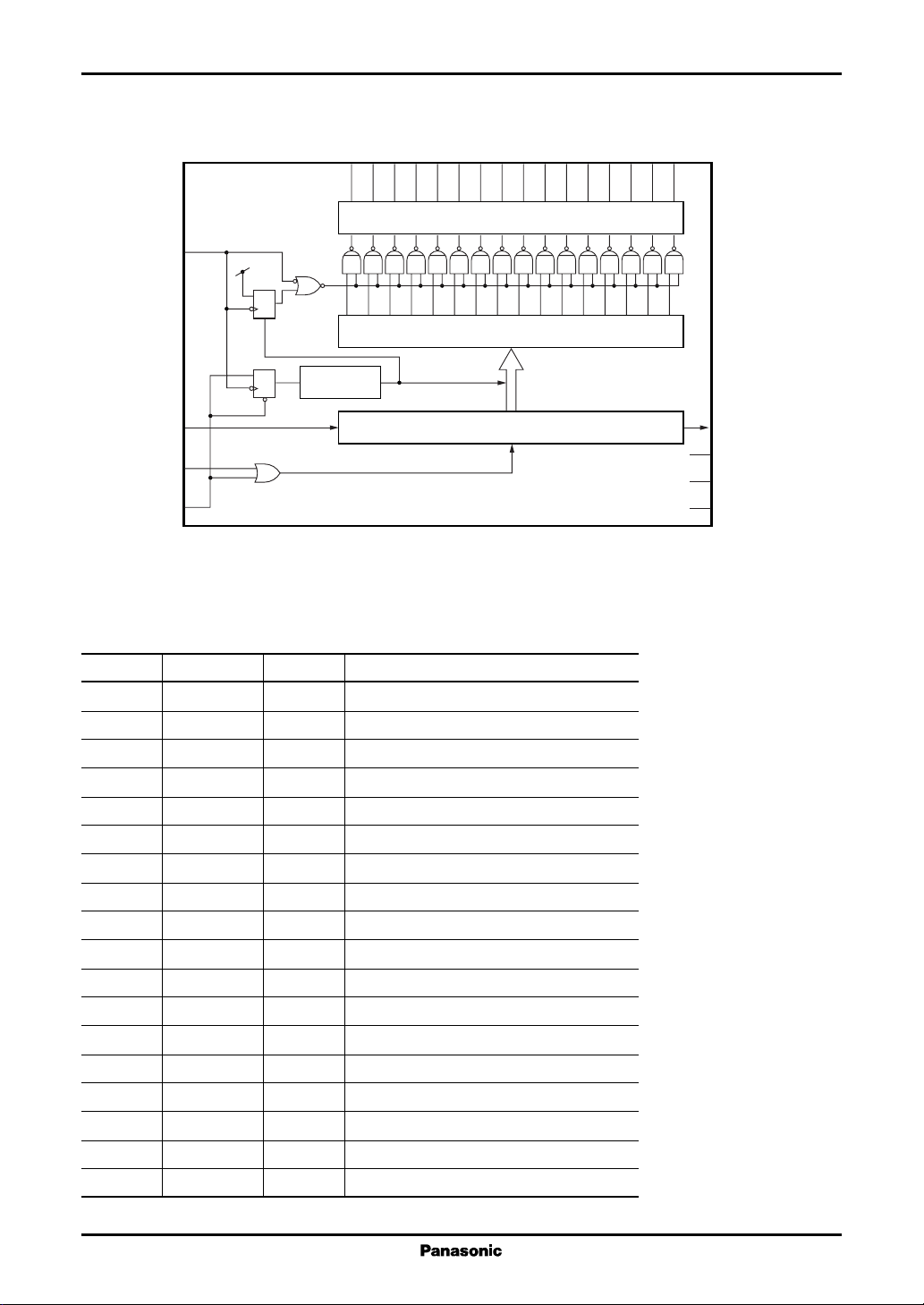
■ Block Diagram
D15
D14
D13
D12
D11
D10D9D8D7D6D5D4D3D2D1D0
9
101112131415161718192021222324
High-voltage handling output ports
3
OE
R
16-bit output data register
CK
16-bit shift register
CK
NSDI
NSCK
NCE
Delay circuit
R
5
6
2
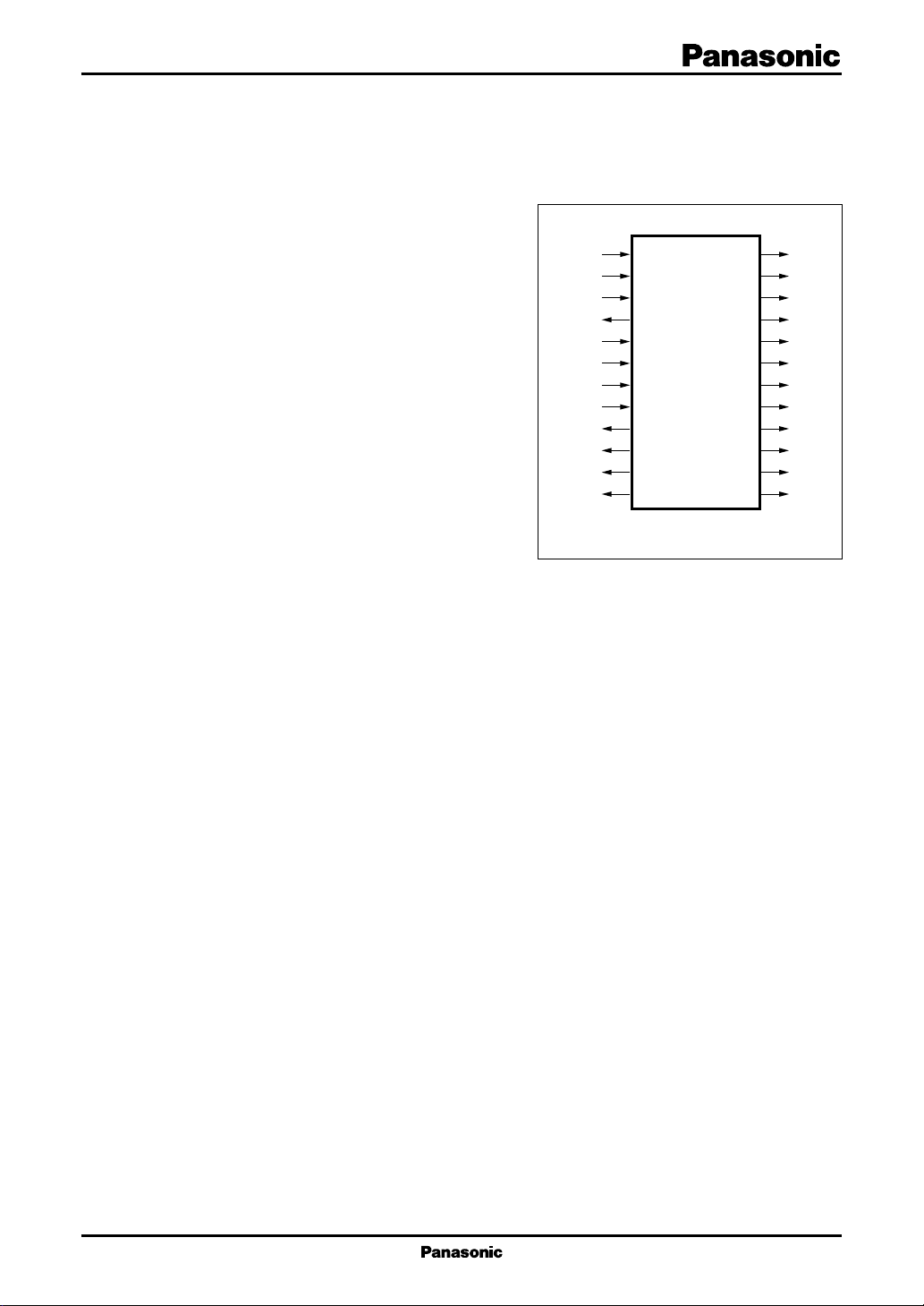
■ Pin Descriptions
Pin No. Symbol I/O Description
1VPPI Pull-down power supply
2 NCE I Chip select input
3 OE I Display on/off state control input
4 NSDO O Serial data output
5 NSDI I Serial data input
6 NSCK I Serial data clock input
7VSSI Ground (display)
8VDDI Power supply
9 D15 O High-voltage output 15
10 D14 O High-voltage output 14
11 D13 O High-voltage output 13
12 D12 O High-voltage output 12
13 D11 O High-voltage output 11
14 D10 O High-voltage output 10
15 D9 O High-voltage output 9
16 D8 O High-voltage output 8
17 D7 O High-voltage output 7
18 D6 O High-voltage output 6
4
8
7
1
NSDO
V
DD
V
SS
V
PP
2
Microcontroller Peripheral LSIs MN12511
■ Pin Descriptions (continued)
Pin No. Symbol I/O Description
19 D5 O High-voltage output 5
20 D4 O High-voltage output 4
21 D3 O High-voltage output 3
22 D2 O High-voltage output 2
23 D1 O High-voltage output 1
24 D0 O High-voltage output 0
■ Operational Description
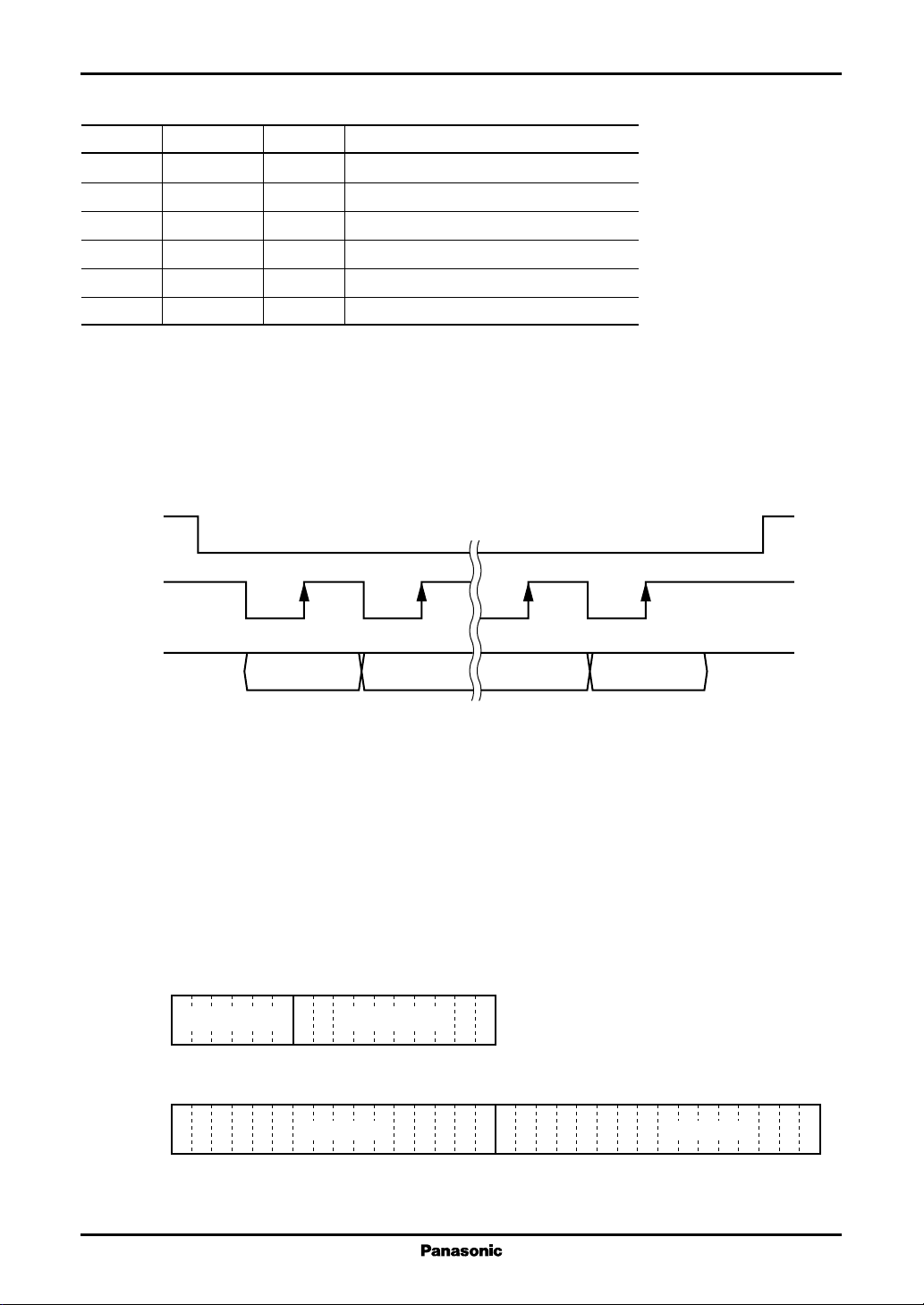
•
Transfer timing
The figure below shows the input timing for the NCE, NSCK, and NSDI pins during data transfers.
NCE
NSCK
NSDI
D15
•
Transfer Format
The following transfer formats could be considered as the data format for data transfer from the system
microcontroller.
Note that other transfer formats are possible, depending on the requirements of the particular application.
Example: For use with a 6-grid × 10-segment display (Using a single MN12511)
6 grid-bit
Example: For use with a 15-grid × 11-segment display (Using two MN12511 chips)
Note) *: Bits marked with an asterisk are unused.
10 segment-bit
15 grid-bit****** 11 segment-bit
D14
D0D1
NSDI is acquired on the rising edge of NSCK.
NSDO is output on the falling edge of NSCK.
3
 Loading...