

Panasonic MN103SFX1K, MN103SFX2K, MN103SFX3K, MN103SFX5K, MN103SFX6K User Manual
...
MN103SFX1K/X2K/X3K/X5K/X6K/X7K
32-bit Single-chip Microcontroller
PubNo. 232X701-015E
1.1 Overview
The MN103S is a 32-bit micro controller combining ease of use intended for programs development in the C language
with a simple, high-performance architecture made possible through pursuit of cost performance.
Built around a compact 32-bit CPU with a basic instruction word length of 1 byte, this LSI includes internal memory for
instructions and data, a clock generator, bus controller, interrupt controller, watchdog timer, standard peripheral circuitry
such as timers and serial interfaces, PWM circuit best suited to controlling 3- phase motors, arithmetic unit for speed-up
of inverter control and analog circuits. (A/D converters and VGA (Variable Gain Amplifier)) for motor position control.
The MN103S Series high-speed CPU coupled with abundance of peripheral features provides an easy means of developing on LSI for motor and power control applications requiring fast response a feature previously unavailable with
conventional micro controllers.
Publication date: April 2018 1
MN103SFX1K/X2K/X3K/X5K/X6K/X7K
32-bit Single-chip Microcontroller
PubNo. 232X701-015E
1.2 Product Summary
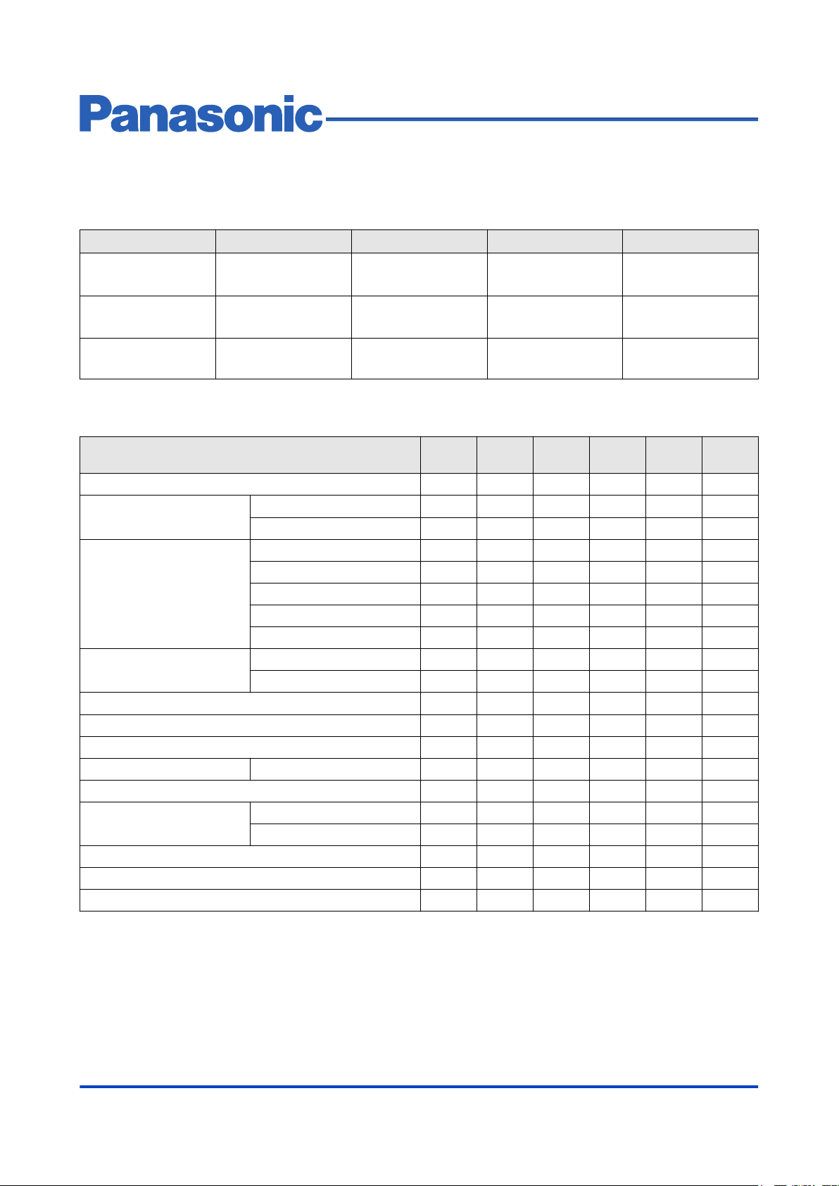
This manual describes LSI in the following Table 1.2-1 .
Table 1.2-1 Product Summary
LSI ROM size RAM size Classification Package
MN103SFX7K / X3K 256 KB 12 KB Flash EEPROM ver-
sion
MN103SFX6K / X2K 256 KB 12 KB Flash EEPROM ver-
sion
MN103SFX5K / X1K 256 KB 12 KB Flash EEPROM ver-
sion
This LSI's functions are listed in Table 1.2-2 .
Table 1.2-2 Functions list
Function MN103S
FX7K
Number of pins 100 80 64 100 80 64
General purpose ports I/O port 74 54 42 82 62 50
Input port 8 8 8 - - -
Special pin Power pin 10 10 8 10 10 8
Reset pin 1 1 1 1 1 1
Oscillation pin 2 2 2 2 2 2
On-board debugger pin 3 3 3 3 3 3
N.C. pin 2 2 - 2 2 -
Interrupt Internal factor 54 54 48 54 54 48
External interrupt 9 9 8 9 9 8
Watchdog Timer 1 1 1 1 1 1
8-bit Timer 12 12 12 12 12 12
16-bit Timer 6 6 4 6 6 4
Serial interface Clock synchronous/ UART 3 3 3 3 3 3
Complementary 3-phase PWM 2 2 2 2 2 2
10-bit A/D converter Number of units 3 3 3 3 3 3
Number of conversion channels 20 16 12 20 16 12
10-bit D/A converter 2 2 2 2 2 2
Variable Gain Amplifier 2 2 2 - - -
Comparator 2 2 2 2 2 2
MN103S
FX6K
MN103S
FX5K
LQFP 100 pin
QFP 100 pin
TQFP 80 pin
LQFP 80 pin
TQFP 64 pin
MN103S
FX3K
MN103S
FX2K
MN103S
FX1K
Publication date: April 2018 2
MN103SFX1K/X2K/X3K/X5K/X6K/X7K
1.3 Features
This LSI's features are described.
CPU (MN103S core)
Structure LOAD/STORE architecture with 5-stage pipeline
Minimum instruction execution cycle
Number of basic instructions
Number of addressing
modes
Basic instruction length 1 byte
Memory space Linear address space of 4 GB (for instructions / data)
Internal memory
Internal ROM capacity 256 KB (Flash Memory)
Sector size Large sector 32 KB (Total 224 KB)
Internal RAM capacity 12 KB
13.9 ns (72 MHz)
(External oscillation frequency 8MHz, 9 multiplying)
46
6
Small sector 8 KB (Total 32 KB)
32-bit Single-chip Microcontroller
PubNo. 232X701-015E
Extended calculation function
Extended calculation instruction
Clock generator
External oscillation (crystal/
ceramic)
Clock multiplying circuit
(PLL)
Operation mode
CPU operation mode NORMAL mode
Standby mode SLEEP mode, HALT mode, STOP mode
Interrupt Controller
Internal interrupt Watchdog timer overflow, System error
External interrupt External interrupt pin input
High-speed multiplication, High-speed division, trigonometric function, absolute value,
square root, LPF, 3-phase/2-phase conversion, PI calculation
Product-sum operation of n-th degree, Saturate calculation
4 to 16 MHz
4 to 12 multiplying
Timer, Serial, PWM, A/D conversion
A/D conversion error detection, Comparator detection
Edge detection or Level detection can be selected
Reset function
Pin reset Control NRST pin from outside
Software reset Writing to register
Power supply detection reset Detection level: 3.6 V to 4.3 V
Publication date: April 2018 3
MN103SFX1K/X2K/X3K/X5K/X6K/X7K
32-bit Single-chip Microcontroller
PubNo. 232X701-015E
Reset function
Error detection reset Error detection by watchdog timer
Watchdog timer
Detection time 8.192 ms to 2097.15 ms (At External oscillation is 8 MHz.)
Function Non-maskable interrupt generates when 1st overflow is detected.
Forced-reset generates in LSI when 2nd overflow is detected.
8-bit timer
Function Interval timer, Timer pulse output, Event count, Baud rate timer, Cascade connection
16-bit timer
Function Interval timer, Event count, Up/Down count, Timer output, PWM output (Cycle varia-
ble, Pulse width variable), Input capture, One-shot output, Start trigger start, Generation
of Start trigger for A/D conversion
Serial interface 0 and 1
Communication mode Clock synchronous serial/ Full duplex UART
Clock synchronous serial Function Parity error detection, Overrun error detection, Specifica-
tion of First transfer bit, Selection of any transfer size
from 7 to 8 bits
Maximum transfer rate 3.0 Mbps
Full duplex UART Function Parity error detection, Overrun error detection, Framing
error detection, Specification of First transfer bit, Selection of any transfer size from 7 to 8 bits
Maximum transfer rate 375 kbps
Serial interface 2
Communication mode Clock synchronous serial/ Full duplex UART
Clock synchronous serial Function Overrun error detection, Specification of First transfer bit,
Selection of any transfer size from 2 to 8 bits
Maximum transfer rate 5.0 Mbps
Full duplex UART Function Parity error detection, Overrun error detection, Framing
error detection, Specification of First transfer bit, Selection of any transfer size from 7 to 8 bits
Maximum transfer rate 300 kbps
Complementary 3-phase PWM timer
Minimum resolution 13.9 ns
Function Triangular wave and saw-tooth wave output, dead time auto-insertion, double buffer up-
date, output protection circuit, output timing variable function
A/D converter
Resolution 10 bits
Number of channels Up to 20 channels in 3 units (There is the share channel.)
Function 16-bit timer, A/D conversion start in synchronization with PWM, Multiple channel con-
version, Conversion channel omitted function, Conversion result error detect function
Publication date: April 2018 4
MN103SFX1K/X2K/X3K/X5K/X6K/X7K
32-bit Single-chip Microcontroller
PubNo. 232X701-015E
D/A converter
Resolution 10 bits
Function Reference of the comparator
VGA (Variable Gain Amplifier)
Gain setting 2 to 20 times
Function Differential input, 3 channels for + side input can be switched (- side is fixed)
Comparator
Function Comparator output cooperates with PWM output. (Pin protection)
Internal flash memory
Rewritable times Large sector (32 KB) 1000 times (Minimum)
Small sector (8 KB) 100000 times (Minimum)
Data retention time 10 years
Package
100 pin LQFP (14 mm square, 0.5 mm pitch, halogen free)
100 pin QFP (18 mm square, 0.65 mm pitch)
80 pin TQFP (12 mm square, 0.5 mm pitch, halogen free)
80 pin LQFP (14 mm square, 0.65 mm pitch, halogen free)
64 pin TQFP (10 mm square, 0.5 mm pitch, halogen free)
* Panasonic "halogen free" semiconductor products refer to the products made of molding resin and interposer which
conform to the following standards.
- Bromine: 900 ppm (Maximum Concentration Value)
- Chlorine: 900 ppm (Maximum Concentration Value)
- Bromine + Chlorine: 1500 ppm (Maximum Concentration Value)
The above-mentioned standards are based on the numerical value described in IEC61249-2-21.
Publication date: April 2018 5
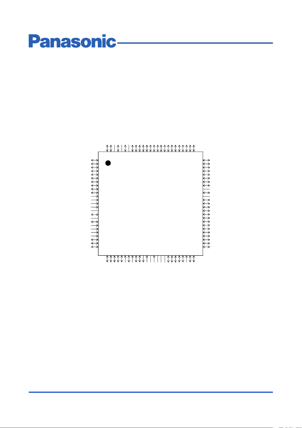
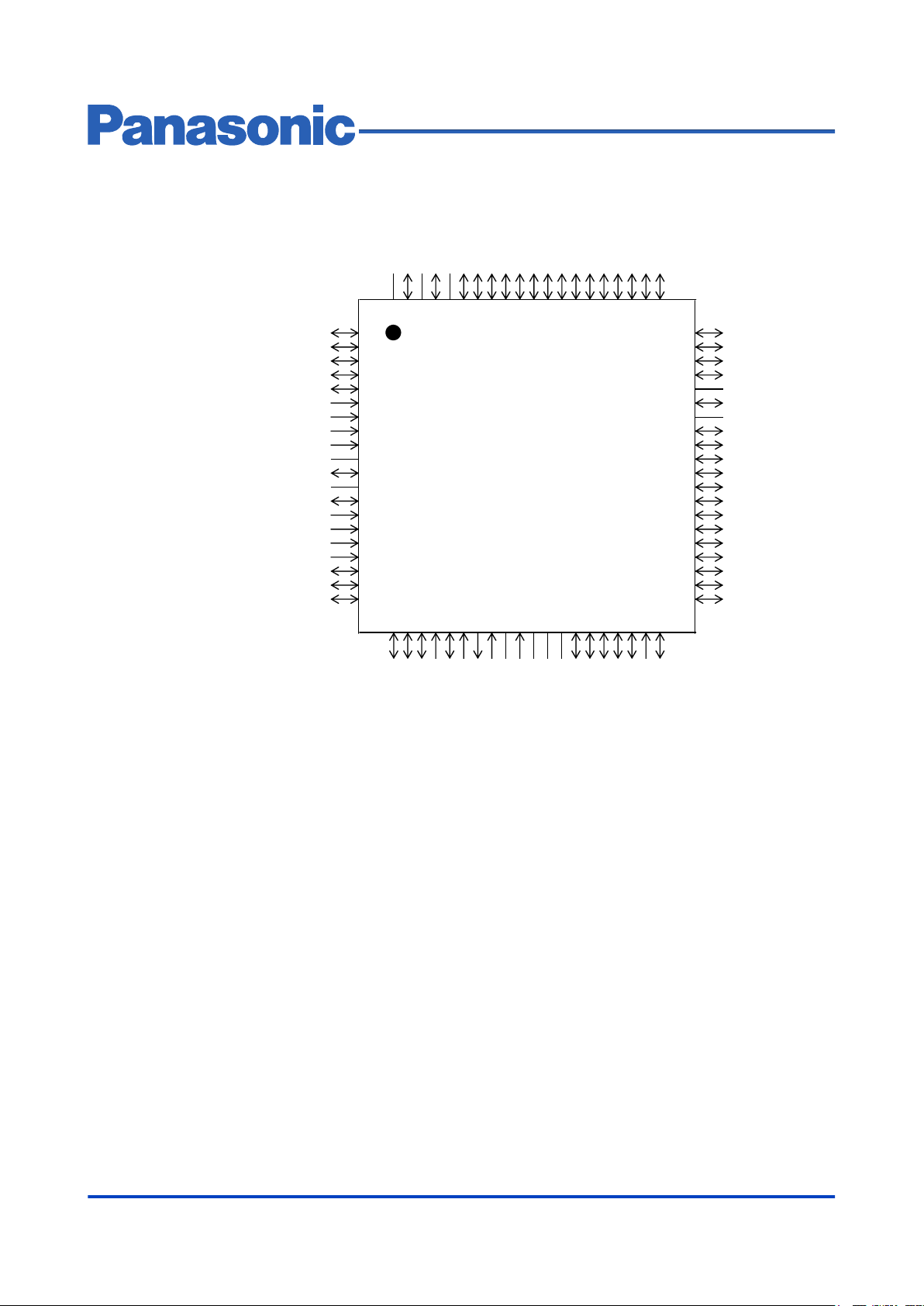
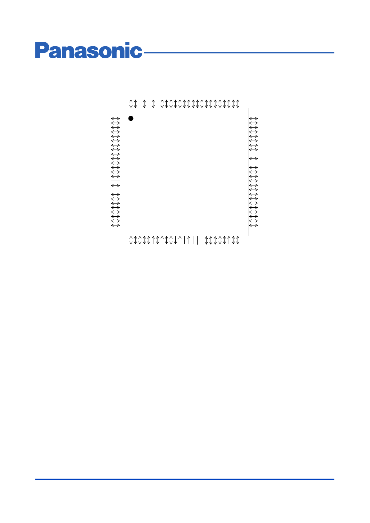
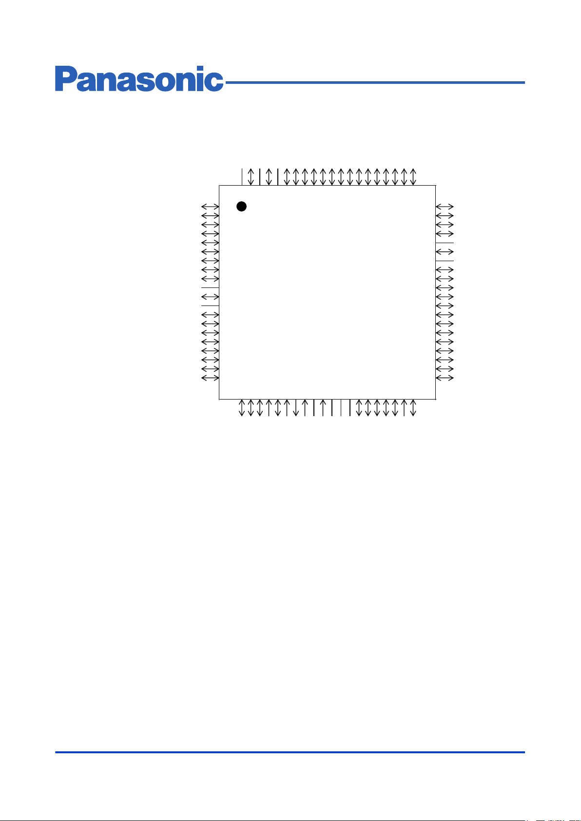
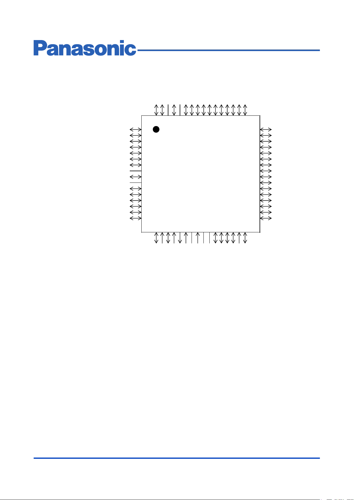
1.4 Pin
6073P23/SBT1
55
54
P30/TM0IO
56
575859
P57/NPWM02
P56/PWM02
P55/NPWM01
P53/NPWM00
P54/PWM01
MN103SFX7K
839594
85
CMP1INA/VGA1P0/ADIN07/P97
AVDD50
EXTRG1/IRQ05/P11
CMP0OUT/IRQ06/P12
P27/SBI0
P26/SBT0
P25/SBO0
P24/SBI1
P22/SBO1
P21/SBI2
TM15IO/P85
P86
6
7
CMP0INB/ADIN05/P95
CMP1REFA/VGA1N/ADIN06/P96
19
12
AVSS
CMP0REFA/VGA0N/ADIN00/P90
72
DA0OUT/CMP0REFB/ADIN04/P94
IRQ01/P81
IRQ02/P82
IRQ03/P83
TM14IO/P84
LQFP 100pin 0.5mm pitch
16913
3226272829
332031
8
P73/TM11IO1
P72/TM11IO0
99
98
3
2
TM11O5/P77
IRQ00/P80
VDD50
P75/TM11O3
P74/TM11O2
N.C.
VSS
TM11O4/P76
97
96
CMP0INA/VGA0P0/ADIN01/P91
11
14
VGA0P1/ADIN02/P92
P63/NPWM10
P66/PWM12
P65/NPWM11
P64/PWM11
P87
1054
1
P60
VGA1P2/ADIN09/PA1
21
VGA1P1/ADIN08/PA0
22
P62/PWM10
P67/NPWM12
939291
74
VGA0P2/ADIN03/P93
100
70
908988
P46/TM10AIO
P52/PWM00
P51/TM7IO
P50/TM6IO
P47/TM10BIO
77
76
P61
P31/TM1IO
P40/TM9AO
P41/TM9BO
P45/TM10BO
75
P44/TM10AO
71
P43/TM9BIO
P42/TM9AIO
VSS
P36/TM8AIO
67
68
P32/TM2IO
64
53522324DA1OUT/CMP1REFB/ADIN10/PA2
626115
1718P17/SBO2
ADIN12/PA4
51
25
CMP1INB/ADIN11/PA3
P20/SBT2
42
P37/TM8BIO
P33/TM3IO
6665P35/TM5IO
VDD50
P34/TM4IO
69
63
ADIN18/PB2
503034353647444541
43
ADIN13/PA5
ADIN14/PA6
ADIN15/PA7
ADIN16/PB0
VDD50
ADIN17/PB1
SCLK
SDATA
NBOOT
TM16IO/P15
TM17IO/P16
493738
OSCI
463940
48
NRST
ADIN19/PB3
OSCO
NTEST
VSS
CMP1OUT/IRQ07/P13
IRQ08/P14
N.C.
VOUT18
EXTRG0/IRQ04/P10
87797882818084
86
QFP 100pin 0.65 mm pitch
The specifications of pins in this LSI are described as follows.
Pin configuration
•
Pin function
•
1.4.1 Pin Configuration
Figure 1.4-1 to Figure 1.4-6 show the pin configuration.
MN103SFX1K/X2K/X3K/X5K/X6K/X7K
32-bit Single-chip Microcontroller
PubNo. 232X701-015E
Publication date: April 2018 6
Figure 1.4-1 Pin Configuration of MN103SFX7K
CMP1OUT/IRQ07/P13
61
70
69
68
67
64
63
38
LQFP 80pin 0.65mm pitch
MN103SFX6K
73
26
27
28
37
77
76
29
30
39
32
33
N.C.
36
34
35
EXTRG0/IRQ04/P10
VOUT18
CMP0OUT/IRQ06/P12
ADIN13/PA5
ADIN14/PA6
ADIN15/PA7
SCLK
SDATA
NRST
NTEST
VDD50
EXTRG1/IRQ05/P11
IRQ08/P14
NBOOT
OSCO
OSCI
VSS
P27/SBI0
P22/SBO1
P23/SBT1
44
42
TM17IO/P16
48
55
21
22
23
24
40
25
45
31
19
DA1OUT/CMP1REFB/ADIN10/PA2
P17/SBO2ADIN12/PA4 4120
P21/SBI2
CMP1INB/ADIN11/PA3 P20/SBT2
4318
46
P33/TM3IO
P34/TM4IO
52
53
P25/SBO0
49
P24/SBI1
P26/SBT0
51
P37/TM8BIO
59
58
57 P36/TM8AIO
VSS
54
47
VDD50
50
P32/TM2IO
P31/TM1IO
P55/NPWM01
P54/PWM0166
65
P35/TM5IO
P43/TM9BIO60
P42/TM9AIO
56
P46/TM10AIO
P53/NPWM00
P52/PWM00
P51/TM7IO
P47/TM10BIO
62
P62/PWM10
VGA1P2/ADIN09/PA1
16VGA1P1/ADIN08/PA0
17
13
CMP1REFA/VGA1N/ADIN06/P96 14
CMP0INB/ADIN05/P95
TQFP 80pin 0.5mm pitch
15
12
CMP1INA/VGA1P0/ADIN07/P97
DA0OUT/CMP0REFB/ADIN04/P94
AVDD50
P56/PWM02
P65/NPWM11
72
71
P57/NPWM02
80
VGA0P2/ADIN03/P93
8
AVSS 10
4
11
3
2IRQ01/P81
IRQ02/P82
CMP0REFA/VGA0N/ADIN00/P90
9
CMP0INA/VGA0P0/ADIN01/P91
6
7
N.C.
VGA0P1/ADIN02/P92
VSS
VDD50
79
78
IRQ03/P83
TM15IO/P85
IRQ00/P80
5
P73/TM11IO1
1
75
74
P64/PWM11
P63/NPWM10
P72/TM11IO0
P67/NPWM12
P66/PWM12
MN103SFX1K/X2K/X3K/X5K/X6K/X7K
32-bit Single-chip Microcontroller
PubNo. 232X701-015E
Publication date: April 2018 7
Figure 1.4-2 Pin Configuration of MN103SFX6K

27
P65/NPWM11
MN103SFX5K
P20/SBT2
CMP1OUT/IRQ07/P13
P21/SBI2
21
25
26
33
P80/IRQ00
VSS
P66/PWM12
P67/NPWM12
VDD50
64
63
62
P54/PWM01
IRQ03/P83
IRQ01/P81
IRQ02/P82
1
3
2
CMP0REFA/VGA0N/ADIN00/P90
CMP0INA/VGA0P0/ADIN01/P91
9
6
7
DA0OUT/CMP0REFB/ADIN04/P94
5
4
CMP1REFA/VGA1N/ADIN06/P96
AVDD50
VGA0P1/ADIN02/P92
VGA0P2/ADIN03/P93
AVSS
12
10
11
8
DA1OUT/CMP1REFB/ADIN10/PA2
TQFP 64pin 0.5mm pitch
CMP0INB/ADIN05/P95
16
VGA1P2/ADIN09/PA1
CMP1INA/VGA1P0/ADIN07/P97
14
15
VGA1P1/ADIN08/PA0
13
P53/NPWM00
P56/PWM02
P55/NPWM01
P64/PWM11
P63/NPWM10
P62/PWM10
P57/NPWM02
48 P46/TM10AIO
52
51
50
49
P52/PWM00
P47/TM10BIO
35
34
38
40
43
42
44
41
CMP1INB/ADIN11/PA3
31
28
P35/TM5IO
P43/TM9BIO
P42/TM9AIO
P34/TM4IO
17
18
19
20
23
24
22
SCLK
SDATA
NBOOT
OSCO
OSCI
SBO2/P17
VSS
NTEST
VDD50
VOUT18
EXTRG0/IRQ04/P10
EXTRG1/IRQ05/P11
29
CMP0OUT/IRQ06/P12
30
NRST
32
P33/TM3IO
P32/TM2IO
P31/TM1IO
P27/SBI0
P22/SBO1
P23/SBT1
P24/SBI1
P26/SBT0
P25/SBO0
47
46
45
36
37
39
53
58
57
56
55
61
60
59
54
MN103SFX1K/X2K/X3K/X5K/X6K/X7K
32-bit Single-chip Microcontroller
PubNo. 232X701-015E
Publication date: April 2018 8
Figure 1.4-3 Pin Configuration of MN103SFX5K
41
43
90898887828180
NRST
CMP0OUT/IRQ06/P12
44
45
OSCO
NTEST
VSS
CMP1OUT/IRQ07/P13
IRQ08/P14
N.C.
VOUT18
EXTRG0/IRQ04/P10
EXTRG1/IRQ05/P11
TM16IO/P15
TM17IO/P16
493738
OSCI
463940
48
ADIN13/PA5
ADIN14/PA6
ADIN15/PA7
ADIN16/PB0
VDD50
ADIN17/PB1
SCLK
SDATA
NBOOT
ADIN19/PB3
VDD50
P34/TM4IO
69
63
ADIN18/PB2
5034353647
P17/SBO2
ADIN12/PA4
51
2542P37/TM8BIO
P33/TM3IO
6665P35/TM5IO
P31/TM1IO
CMP1IN/ADIN11/PA3
P20/SBT2
53522324DA1OUT/CMP1REF/ADIN10/PA2
ADIN09/PA1
217074
6261VSS
P36/TM8AIO
67
68
P32/TM2IO
64
P61
P60
P40/TM9AO
P41/TM9BO
P45/TM10BO
75
P44/TM10AO
71
P43/TM9BIO
P42/TM9AIO
P46/TM10AIO
P52/PWM00
P51/TM7IO
P50/TM6IO
P47/TM10BIO
777679
78
ADIN08/PA0
22
ADIN03/P93
100
P62/PWM10
P67/NPWM12
939291
P63/NPWM10
P66/PWM12
P65/NPWM11
P64/PWM11
P87
10
15
12
AVSS
ADIN00/P90
ADIN01/P91
ADIN02/P92
TM11O4/P76
54132
TM11O5/P77
IRQ00/P80
8
P73/TM11IO1
P72/TM11IO0
99
98
VDD50
P75/TM11O3
P74/TM11O2
N.C.
VSS
1711141816913
96
86
31322627282930
19
20
33
839594
LQFP 100pin 0.5mm pitch
858497
72
DA0OUT/CMP0REF/ADIN04/P94
IRQ01/P81
IRQ02/P82
IRQ03/P83
TM14IO/P84
TM15IO/P85
P86
6
7
P21/SBI2
P23/SBT1
CMP0IN/ADIN05/P95
ADIN06/P96
ADIN07/P97
AVDD50
56
57585960P27/SBI0
P26/SBT0
P25/SBO0
P24/SBI1
P22/SBO1
73
55
54
P30/TM0IO
P57/NPWM02
P56/PWM02
P55/NPWM01
P53/NPWM00
P54/PWM01
MN103SFX3K
QFP 100pin 0.65 mm pitch
MN103SFX1K/X2K/X3K/X5K/X6K/X7K
32-bit Single-chip Microcontroller
PubNo. 232X701-015E
Figure 1.4-4 Pin Configuration of MN103SFX3K
Publication date: April 2018 9
LQFP 80pin 0.65mm pitch
75
74
P64/PWM11
P63/NPWM10
P72/TM11IO0
P67/NPWM12
P66/PWM12
N.C.
P73/TM11IO1
VSS
VDD50
79
78
IRQ03/P83
TM15IO/P85
IRQ00/P80
5
4
1
3
2IRQ01/P81
IRQ02/P82
ADIN00/P90
9
ADIN01/P91
6
7
ADIN02/P92
ADIN03/P93
8
10
15
12
ADIN07/P97
DA0OUT/CMP0REF/ADIN04/P94
AVDD50
11
14
CMP0IN/ADIN05/P95
16ADIN08/PA0
17
P56/PWM02
P65/NPWM11
72
71
P57/NPWM02
P62/PWM10
AVSS
13
ADIN06/P96
80
P46/TM10AIO
P53/NPWM00
P52/PWM00
P51/TM7IO
P47/TM10BIO
62
P55/NPWM01
P54/PWM01
66
65
P35/TM5IO
VSS
P43/TM9BIO60
P42/TM9AIO
56
P37/TM8BIO
53
P25/SBO0
49
P24/SBI1
59
58
57 P36/TM8AIO
VDD50
P23/SBT145
44
47
46
P33/TM3IO52
P26/SBT0
51
50
18
19
DA1OUT/CMP1REF/ADIN10/PA2
P22/SBO1
P21/SBI2
ADIN09/PA1
P17/SBO2ADIN12/PA4 4120
CMP1IN/ADIN11/PA3 P20/SBT242
P32/TM2IO
P31/TM1IO
P27/SBI0
54
48
P34/TM4IO
VSS
55
21
22
23
24
40
25
29
43
ADIN13/PA5
ADIN14/PA6
ADIN15/PA7
SCLK
NBOOT
OSCO
SDATA
NRST
TM17IO/P16
39
32
33
N.C.
36
34
35EXTRG1/IRQ05/P11
MN103SFX2K
73
26
27
28
37
77
76
30
31
IRQ08/P14
CMP0OUT/IRQ06/P12
CMP1OUT/IRQ07/P13
38
TQFP 80pin 0.5mm pitch
NTEST
VDD50
EXTRG0/IRQ04/P10
VOUT18
OSCI
61
70
69
68
67
64
63
MN103SFX1K/X2K/X3K/X5K/X6K/X7K
32-bit Single-chip Microcontroller
PubNo. 232X701-015E
Publication date: April 2018 10
Figure 1.4-5 Pin Configuration of MN103SFX2K
59
54
53
58
57
56
55
47
46
45
36
37
39
NRST
P33/TM3IO
P32/TM2IO
P31/TM1IO
P27/SBI0
P22/SBO1
P23/SBT1
P24/SBI1
P26/SBT0
P25/SBO0
SBO2/P17 32
VDD50
VOUT18
EXTRG0/IRQ04/P10
EXTRG1/IRQ05/P11
29
CMP0OUT/IRQ06/P12
30
OSCO
OSCI
VSS
NTEST
CMP1IN/ADIN11/PA3
SCLK
SDATA
NBOOT
23
24
31
28
17
18
19
20
22
27
P35/TM5IO
P43/TM9BIO
P42/TM9AIO
P34/TM4IO
P52/PWM00
P47/TM10BIO
35
34
38
40
43
42
44
41
48 P46/TM10AIO
52
51
50
49
P64/PWM11
P63/NPWM10
P62/PWM10
P57/NPWM02
P54/PWM01
P53/NPWM00
P56/PWM02
P55/NPWM01
DA1OUT/CMP1REF/ADIN10/PA2
TQFP 64pin 0.5mm pitch
CMP0IN/ADIN05/P95
16
ADIN09/PA1
ADIN07/P97
14
15
ADIN08/PA0
13
12
10
11
8
ADIN06/P96
AVDD50
AVSS
ADIN00/P90
ADIN01/P91
9
6
7
DA0OUT/CMP0REF/ADIN04/P94
5
4
ADIN02/P92
ADIN03/P93
IRQ03/P83
IRQ01/P81
IRQ02/P82
1
3
2
P80/IRQ00
VSS
P66/PWM12
P67/NPWM12
VDD50
64
63
62
61
60
P65/NPWM11
MN103SFX1K
P20/SBT2
CMP1OUT/IRQ07/P13
P21/SBI2
21
25
26
33
MN103SFX1K/X2K/X3K/X5K/X6K/X7K
32-bit Single-chip Microcontroller
PubNo. 232X701-015E
Publication date: April 2018 11
Figure 1.4-6 Pin Configuration of MN103SFX1K

MN103SFX1K/X2K/X3K/X5K/X6K/X7K
32-bit Single-chip Microcontroller
PubNo. 232X701-015E
1.4.2 Pin Function
The pin function tables of each series are shown in the following order.
Pin function table in MN103SFX7K series (Table 1.4-1 )
•
Pin function table in MN103SFX6K series (Table 1.4-2 )
•
Pin function table in MN103SFX5K series (Table 1.4-3 )
•
Pin function table in MN103SFX3K series (Table 1.4-4 )
•
Pin function table in MN103SFX2K series (Table 1.4-5 )
•
Pin function table in MN103SFX1K series (Table 1.4-6 )
•
Hint:
When designing a board, resistor and capacity should be connected to the pins (power supply, GND, function control, clock, reset, on-board debug function, and Unused). Refer to [Chapter Overview] of LSI User's Manual for the
value of resistor and capacity/
Publication date: April 2018 12
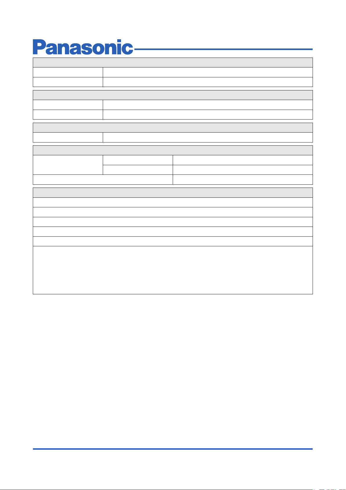
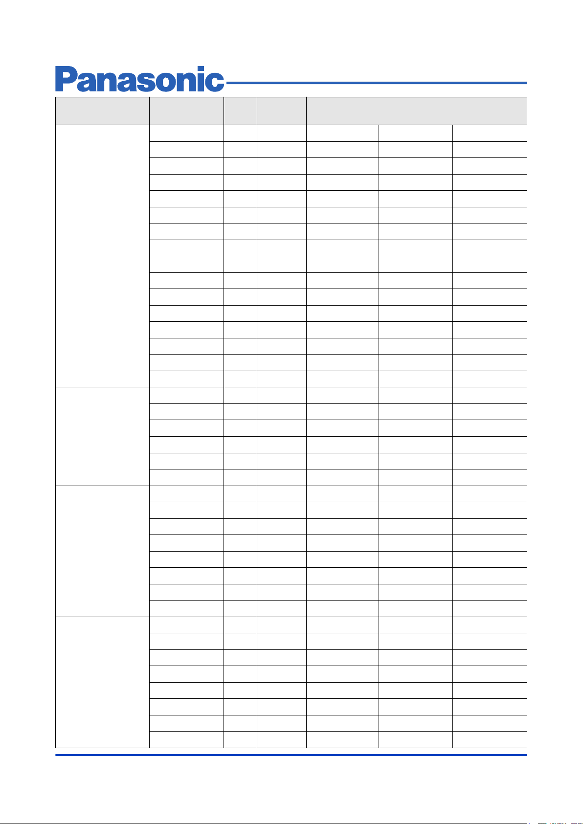
1.4.2.1 Pin Function Table in MN103SFX7K Series
Pin function table in MN103SFX7K series is shown in Table 1.4-1 .
Table 1.4-1 Pin function table in MN103SFX7K series
MN103SFX1K/X2K/X3K/X5K/X6K/X7K
32-bit Single-chip Microcontroller
PubNo. 232X701-015E
Function Pin Name Pin
I/O Other Pins
No.
Power supply pin for
digital I/O
VDD50 40 Input
65
94
Power supply pin for
AVDD50 17 Input
analog
GND pin for digital VSS 38 Input
67
96
GND pin for analog AVSS 15 Input
Power supply output
VOUT18 42 Output
pin for internal circuit
Test signal input pin NTEST 39 Input
Start sector control pin NBOOT 33 Input
Reset signal input pin
NRST 48 I/O
(negative logic)
High-speed oscillation
OSCI 37 Input
input pin
High-speed oscillation
OSCO 36 Output
output pin
External interrupt
input pin
IRQ00 3 Input P80
IRQ01 4 Input P81
IRQ02 5 Input P82
IRQ03 6 Input P83
IRQ04 43 Input P10 EXTRG0
IRQ05 44 Input P11 EXTRG1
IRQ06 45 Input P12 CMP0OUT
IRQ07 46 Input P13 CMP1OUT
IRQ08 47 Input P14
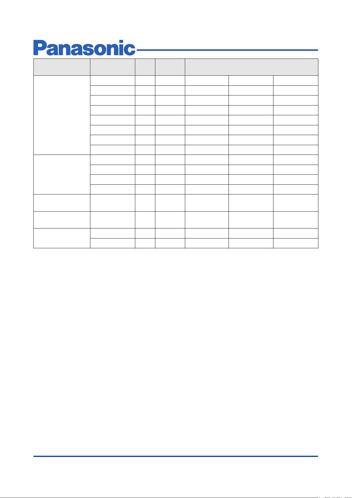
Publication date: April 2018 13

MN103SFX1K/X2K/X3K/X5K/X6K/X7K
32-bit Single-chip Microcontroller
PubNo. 232X701-015E
Function Pin Name Pin
I/O Other Pins
No.
8-bit timer I/O pin TM0IO 60 I/O P30
TM1IO 61 I/O P31
TM2IO 62 I/O P32
TM3IO 63 I/O P33
TM4IO 64 I/O P34
TM5IO 66 I/O P35
TM6IO 78 I/O P50
TM7IO 79 I/O P51
TM14IO 7 I/O P84
TM15IO 8 I/O P85
TM16IO 49 I/O P15
TM17IO 50 I/O P16
16-bit timer I/O pin TM8AIO 68 I/O P36
TM8BIO 69 I/O P37
TM9AO 70 Output P40
TM9BO 71 Output P41
TM9AIO 72 I/O P42
TM9BIO 73 I/O P43
TM10AO 74 Output P44
TM10BO 75 Output P45
TM10AIO 76 I/O P46
TM10BIO 77 I/O P47
TM11IO0 95 I/O P72
TM11IO1 97 I/O P73
TM11O2 99 Output P74
TM11O3 100 Output P75
TM11O4 1 Output P76
TM11O5 2 Output P77
Publication date: April 2018 14
MN103SFX1K/X2K/X3K/X5K/X6K/X7K
32-bit Single-chip Microcontroller
PubNo. 232X701-015E
Function Pin Name Pin
I/O Other Pins
No.
Motor control 3-phases PWM signal I/O
pin
PWM00 80 Output P52
NPWM00 81 Output P53
PWM01 82 Output P54
NPWM01 83 Output P55
PWM02 84 Output P56
NPWM02 85 Output P57
PWM10 88 Output P62
NPWM10 89 Output P63
PWM11 90 Output P64
NPWM11 91 Output P65
PWM12 92 Output P66
NPWM12 93 Output P67
Serial clock I/O pin SBT0 58 I/O P26
SBT1 55 I/O P23
SBT2 52 I/O P20
SBO0 57 Output P25
SBO1 54 Output P22
SBO2 51 I/O P17
SBI0 59 Input P27
SBI1 56 Input P24
SBI2 53 Input P21
Publication date: April 2018 15

MN103SFX1K/X2K/X3K/X5K/X6K/X7K
32-bit Single-chip Microcontroller
PubNo. 232X701-015E
Function Pin Name Pin
I/O Other Pins
No.
Analog input pin for
A/D converter
ADIN00 11 Input P90 VGA0N CMP0REFA
ADIN01 12 Input P91 VGA0P0 CMP0INA
ADIN02 13 Input P92 VGA0P1
ADIN03 14 Input P93 VGA0P2
ADIN04 16 Input P94 CMP0REFB DA0OUT
ADIN05 18 Input P95 CMP0INB
ADIN06 19 Input P96 VGA1N CMP1REFA
ADIN07 20 Input P97 VGA1P0 CMP1INA
ADIN08 21 Input PA0 VGA1P1
ADIN09 22 Input PA1 VGA1P2
ADIN10 23 Input PA2 CMP1REFB DA1OUT
ADIN11 24 Input PA3 CMP1INB
ADIN12 25 Input PA4
ADIN13 26 Input PA5
ADIN14 27 Input PA6
ADIN15 28 Input PA7
ADIN16 29 Input PB0
ADIN17 30 Input PB1
ADIN18 34 Input PB2
ADIN19 35 Input PB3
Analog input pin for
VGA
VGA0N 11 Input P90 ADIN00 CMP0REFA
VGA0P0 12 Input P91 ADIN01 CMP0INA
VGA0P1 13 Input P92 ADIN02
VGA0P2 14 Input P93 ADIN03
VGA1N 19 Input P96 ADIN06 CMP1REFA
VGA1P0 20 Input P97 ADIN07 CMP1INA
VGA1P1 21 Input PA0 ADIN08
VGA1P2 22 Input PA1 ADIN09
Comparator reference
voltage input pin
CMP0REFA 11 Input P90 ADIN00 VGA0N
CMP0REFB 16 Input P94 ADIN04 DA0OUT
CMP1REFA 19 Input P96 ADIN06 VGA1N
CMP1REFB 23 Input PA2 ADIN10 DA1OUT
Comparator input pin CMP0INA 12 Input P91 ADIN01 VGA0P0
CMP0INB 18 Input P95 ADIN05
CMP1INA 20 Input P97 ADIN07 VGA1P0
CMP1INB 24 Input PA3 ADIN11
Comparator output pin CMP0OUT 45 Output P12 IRQ06
CMP1OUT 46 Output P13 IRQ07
Publication date: April 2018 16
MN103SFX1K/X2K/X3K/X5K/X6K/X7K
32-bit Single-chip Microcontroller
PubNo. 232X701-015E
Function Pin Name Pin
No.
D/A converter output
pin
General-purpose I/O
Port 1
DA0OUT 16 Output P94 ADIN04 CMP0REFB
DA1OUT 23 Output PA2 ADIN10 CMP1REFB
P10 43 I/O IRQ04 EXTRG0
P11 44 I/O IRQ05 EXTRG1
P12 45 I/O IRQ06 CMP0OUT
P13 46 I/O IRQ07 CMP1OUT
P14 47 I/O IRQ08
P15 49 I/O TM16IO
P16 50 I/O TM17IO
P17 51 I/O SBO2
General-purpose I/O
Port 2
P20 52 I/O SBT2
P21 53 I/O SBI2
P22 54 I/O SBO1
P23 55 I/O SBT1
P24 56 I/O SBI1
P25 57 I/O SBO0
P26 58 I/O SBT0
P27 59 I/O SBI0
General-purpose I/O
Port 3
P30 60 I/O TM0IO
P31 61 I/O TM1IO
P32 62 I/O TM2IO
P33 63 I/O TM3IO
P34 64 I/O TM4IO
P35 66 I/O TM5IO
P36 68 I/O TM8AIO
P37 69 I/O TM8BIO
General-purpose I/O
Port 4
P40 70 I/O TM9AO
P41 71 I/O TM9BO
P42 72 I/O TM9AIO
P43 73 I/O TM9BIO
P44 74 I/O TM10AO
P45 75 I/O TM10BO
P46 76 I/O TM10AIO
P47 77 I/O TM10BIO
I/O Other Pins
Publication date: April 2018 17
MN103SFX1K/X2K/X3K/X5K/X6K/X7K
32-bit Single-chip Microcontroller
PubNo. 232X701-015E
Function Pin Name Pin
No.
General-purpose I/O
Port 5
P50 78 I/O TM6IO
P51 79 I/O TM7IO
P52 80 I/O PWM00
P53 81 I/O NPWM00
P54 82 I/O PWM01
P55 83 I/O NPWM01
P56 84 I/O PWM02
P57 85 I/O NPWM02
General-purpose I/O
Port 6
P60 86 I/O
P61 87 I/O
P62 88 I/O PWM10
P63 89 I/O NPWM10
P64 90 I/O PWM11
P65 91 I/O NPWM11
P66 92 I/O PWM12
P67 93 I/O NPWM12
General-purpose I/O
Port 7
P72 95 I/O TM11IO0
P73 97 I/O TM11IO1
P74 99 I/O TM11O2
P75 100 I/O TM11O3
P76 1 I/O TM11O4
P77 2 I/O TM11O5
General-purpose I/O
Port 8
P80 3 I/O IRQ00
P81 4 I/O IRQ01
P82 5 I/O IRQ02
P83 6 I/O IRQ03
P84 7 I/O TM14IO
P85 8 I/O TM15IO
P86 9 I/O
P87 10 I/O
General-purpose I/O
Port 9
P90 11 Input ADIN00 VGA0N CMP0REFA
P91 12 Input ADIN01 VGA0P0 CMP0INA
P92 13 Input ADIN02 VGA0P1
P93 14 Input ADIN03 VGA0P2
P94 16 I/O ADIN04 CMP0REFB DA0OUT
P95 18 I/O ADIN05 CMP0INB
P96 19 Input ADIN06 VGA1N CMP1REFA
P97 20 Input ADIN07 VGA1P0 CMP1INA
I/O Other Pins
Publication date: April 2018 18
MN103SFX1K/X2K/X3K/X5K/X6K/X7K
32-bit Single-chip Microcontroller
PubNo. 232X701-015E
Function Pin Name Pin
No.
General-purpose I/O
Port A
PA0 21 Input ADIN08 VGA1P1
PA1 22 Input ADIN09 VGA1P2
PA2 23 I/O ADIN10 CMP1REFB DA1OUT
PA3 24 I/O ADIN11 CMP1INB
PA4 25 I/O ADIN12
PA5 26 I/O ADIN13
PA6 27 I/O ADIN14
PA7 28 I/O ADIN15
General-purpose I/O
Port B
PB0 29 I/O ADIN16
PB1 30 I/O ADIN17
PB2 34 I/O ADIN18
PB3 35 I/O ADIN19
Clock input pin for
SCLK 31 Input
on-board debugger
Data I/O pin for on-
SDATA 32 I/O
board debugger
Trigger I/O pin for onboard debugger
EXTRG0 43 I/O P10 IRQ04
EXTRG1 44 I/O P11 IRQ05
I/O Other Pins
Publication date: April 2018 19
 Loading...