

Panasonic MN103S, MN103SA7D, MN103SA7G User Manual

Cover
MICROCOMPUTER MN103S
MN103SA7D/A7G
LSI User’s Manual
Pub.No.232A7-012E


Request for your special attention and precautions in using the technical information and
semiconductors described in this book
(1) If any of the products or technical information described in this book is to be exported or provided to non-residents, the
laws and regulations of the exporting country, especially, those with regard to security export control, must be observed .
(2) The technical information described in this book is intended only to show the main characteristics and applicat ion cir cuit
examples of the products, and no license is granted under any intellectual property right or other right owned by our
company or any other company. Therefore, no responsibility is assumed by our company as to the infringement upon any
such right owned by any other company which may arise as a result of the use of technical information described in this
book.
(3) The products described in this book are intended to be used for standard applications or general electronic equipment
(such as office equipment, communications equipment, measuring ins truments and household appliances).
Consult our sales staff in advance for information on the following applications:
x Special applications (such as for airplanes, aerospace, automobiles, traffic control equipment, combustion equipment,
life support systems and safety devices) in which exceptional quality and reliability are required, or if the failure or
malfunction of the products may directly jeopardize life or harm the human body.
x Any applications other than the standard applications intended.
(4) The products and product specifications described in this book are subject to change without notice for modification and/
or improvement. At the final stage of your de sign, pur chasing, o r use of the p roducts, therefore , ask for the mo st up-todate Product Standards in advance to make sure that the latest specifications satisfy your requirements.
(5) When designing your equipment, comply with the range of absolute maximum rating and the guaranteed operating condi-
tions (operating power supply voltage and operating environment etc.). Especially, please be careful not to exceed the
range of absolute maximum rating on the transient state, such as power-on, power-off and mode-switching. Otherwise,
we will not be liable for any defect which may arise later in your equipment.
Even when the products are used within the guaranteed values, take into the consideration of incidence of break down
and failure mode, possible to occur to semiconductor products. Measures on the systems such as redundant design,
arresting the spread of fire or preventing glitch are recommended in order to prevent physical injury, fire, social damages, for example, by using the products.
(6) Comply with the instructions for use in order to prevent breakdown and characteristics change due to external factors
(ESD, EOS, thermal stress and mechanical stress) at the time of handling, mounting or at customer's process. When
using products for which damp-proof packing is required, satisfy the conditions, such as shelf life and the elapsed time
since first opening the packages.
(7) This book may be not reprinted or reproduced whether wholly or partially, without the prior written permission of Mat-
sushita Electric Industrial Co., Ltd.
If you have any inquiries or questions about this book or our semiconductor products, please contact one of
our sales offices listed on the back or Semiconductor Company's Department.
MS-DOS is a registered trademark of Microsoft Corporation.
Windows is a trademark of Microsoft Corporation.
PanaXSeries is a trademark of Matsushita Electric Industrial Co., Ltd.
The other corporation names, logotype and product names written in this book are trademarks or registered trademarks
of their corresponding corporations.

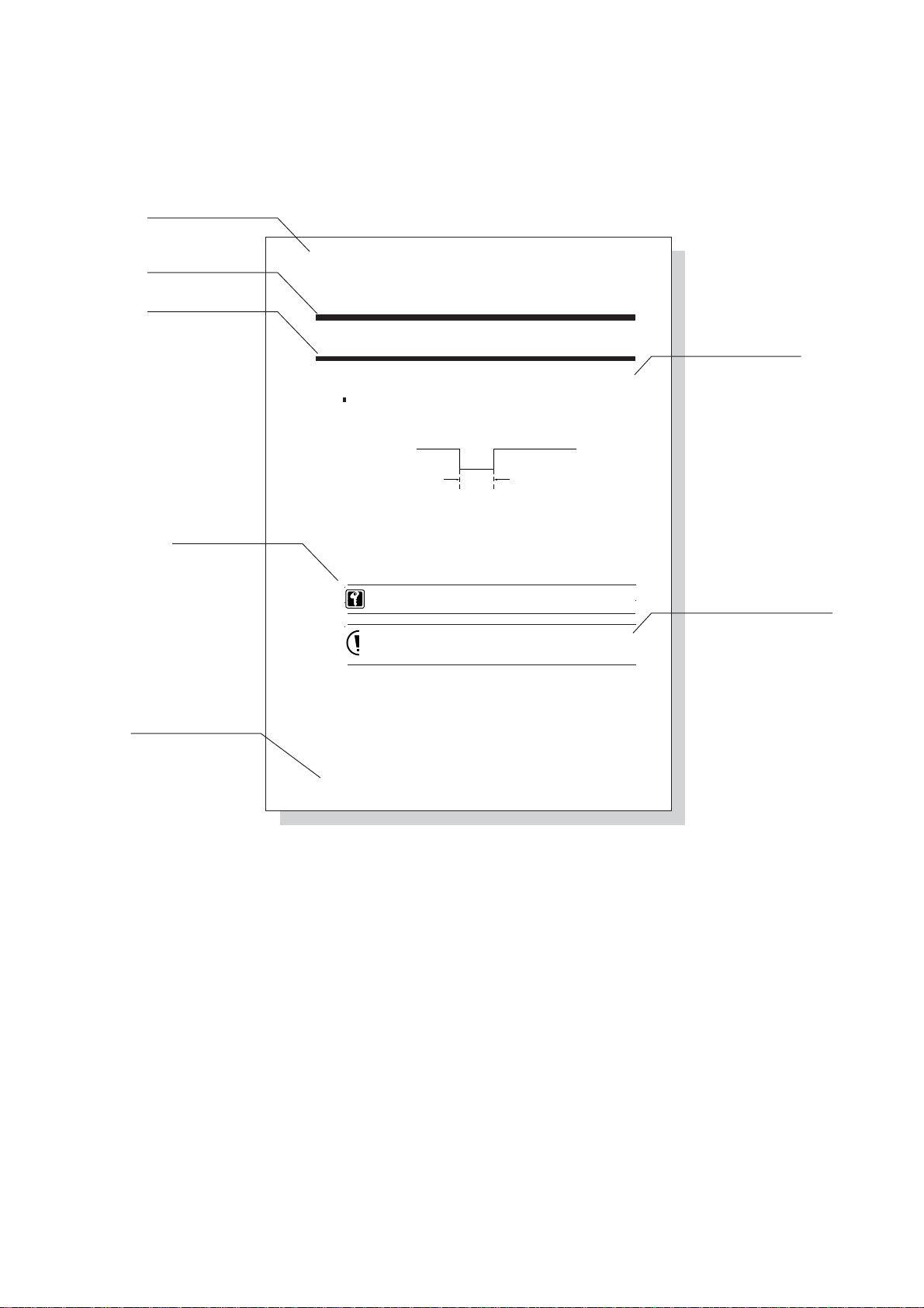
About This Manual
■
Organization
This LSI manual describes the features of the MN103SA7 Series, which begins with an overview, followed by information in the order of CPU basic, interrupt, port, timer, serial, and other peripheral
hardware functions.
Each section consists of brief functional information, block diagrams, and the details of control registers
including operation methods and setting examples.
<About This Manual - 1>
■
Manual Configuration
Each section of this manual consists of a title, summary, main text, key information, precautions and
warnings, and references.The layout and definition of each section are shown below.
Header
Chapter number and
Chapter title
Section title
chapter 2
Basic CPU
Sub section title
Key information
Important information
from the text.
footer
Page # and
section title.
2.8 Reset
2.8.1 Reset operation
the CPU contents are reset and registers are intialized when the NRST pin (P
27) is pulled to low.
Initiating a Reset
There are two methods to initiate areset.
(1) Drive the NRST pin low for at least four clock cycles.
NTST pin should be holded "low" for more than 4 clock cycles (200 ns a
t a 20 NHz)
NRST pin
4 clock cycles
(200 ns at a 20 MHz)
Figure:2.8.1 MInimum Reset PUlse Width
(2 Setting the P2OUT7 flag of the P2OUT register to "0" outputs low level at P
27 (NRST) pin. And transfering to reset by program (software reset) can be
executed. If the internal LSI is reset and register is initiated, the P2OUT
7 flag becomes "1" and reset is released.
On this LSI, the starting mode is NORMAL mode that high oscillation i
s the base clock.
When the power voltage low circuit is connected to NTST pin, circuit t
hat gives pulse for enough low level time at sudeen unconnected. And r
set can be generated even if its pulse is low level as the oscillation
clock is under 4 clocks,take notice of noise.
Main text
Precautions and
warnings
Precautions are listed
in case.
Be sure to read these
of lost functionality
or damage.
II-48 Reset
Note: The example on this page is for explanation. It differs from an actual page.
<About This Manual - 2>

■
Finding Desired Information
This manual provides three methods for finding desired information quickly and easily.
1.Consult the index at the front of the manual to locate the beginning of each section.
2.Consult the table of contents at the front of the manual to locate desired titles.
3.A chapter number and its chapter title are located at the top corner of each page, and section titles are
located at the bottom corner of each page.
Related Manuals
■
Note that the following related documents are available.
• "MN103S Series Instruction Manual"
<Describes the instruction set.>
• "MN103S Series Cross-assembler User's Manual"
<Describes the assembler syntax and notation.>
• " Series C Compiler User's Manual: Usage Guide"
<Describes the installation, the commands, and options of the C Compiler.>
• "MN103S Series C Compiler User's Manual: Language Description"
<Describes the syntax of the C Compiler.>
• "MN103S Series C Compiler User's Manual: Library Reference"
<Describes the standard library of the C Compiler.>
• "MN103S Series C Source Code Debugger User's Manual"
<Describes the use of C source code debugger.>
• "MN103S Series Installation Manual"
<Describes the installation of C compiler, cross-assembler and C source code debugger and the
procedure for bringing up the in-circuit emulator.>
<About This Manual - 3>

Chapter Table
Contents
Chapter 1 Overview
Chapter 2 CPU Basics
Chapter 3 Clock Generator
Chapter 4 Bus Controller
Chapter 5 Interrupt Controller
0
1
2
3
4
5
Chapter 6 ROM Correction
Chapter 7 I/O Ports
Chapter 8 8-bit Timer
Chapter 9 16-bit Timer
Chapter 10 Motor Control PWM
Chapter 11 Watchdog Timer
6
4
8
9
10
11
Chapter 12 Serial Interface 0 and 1
12


Chapter 13 Serial Interface 2
13
Chapter 14 A/D Converter
Chapter 15 Regulator
Chapter 16 Appendix
14
15
16


Contents
Contents
0

Contents
Chapter 1 Overview................................................................................................................ 1-1
1.1 Overview ............................................................................................................................................. 1-2
1.1.1 Overview............................................................................................................................. .. 1-2
1.1.2 Product Summary .................................................................................................................. 1-2
1.2 Hardware Functions............................................................................................................................. 1-3
1.3 Pin Description.................................................................................................................................... 1-9
1.3.1 Pin Configuration.................................................................................................................. 1-9
1.3.2 Pin Specification ................................................................................................................. 1-10
1.3.3 Pin Functions....................................................................................................................... 1-12
1.4 Block Diagram................................................................................................................................... 1-16
1.4.1 Block Diagram.................................................................................................................... 1-16
1.5 Electrical Characteristics................................................................................................................... 1-17
1.5.1 Absolute Maximum Ratings ............................................................................................... 1-17
1.5.2 Operating Conditions.......................................................................................................... 1-18
1.5.3 DC Characteristics .............................................................................................................. 1-20
1.5.4 A/D Converter Characteristics............................................ ................................................ 1-22
1.5.5 AC Characteristics .............................................................................................................. 1-23
1.6 Package Dimension........................................................................................................................... 1-26
Chapter 2 CPU Basics ............................................................................................................ 2-1
2.1 Overview ............................................................................................................................................. 2-2
2.2 Block Diagram..................................................................................................................................... 2-3
2.3 Programming Model.................................................................................................................. .......... 2-5
2.3.1 CPU Registers....................................................................................................................... 2-5
2.3.2 Control Registers................................................................................................................... 2-8
2.4 Data Formats ....................................................................................................................................... 2-9
2.5 Instructions........................................................................................................................................ 2-10
2.5.1 Instruction Format............................................................................................................... 2-10
2.5.2 Addressing Modes............................................................................................................... 2-12
2.5.3 Instruction Set ..................................................................................................................... 2-13
2.6 Memory Space................................................................................................................................... 2-17
2.6.1 Overview............................................................................................................................. 2-17
2.6.2 Memory Map....................................................................................................................... 2-18
2.6.3 Register Map....................................................................................................................... 2-19
<Contents - 2>

2.7 Operation Mode ........................................................................... ..................................................... 2-21
2.7.1 Overview............................................................................................................................. 2-21
2.7.2 Reset Status......................................................................................................................... 2-21
Chapter 3 Clock Generator..................................................................................................... 3-1
3.1 Overview....................................................... ................................................................. ..................... 3-2
3.1.1 Functions............................................................................................................................... 3-2
3.1.2 Block Diagram...................................................................................................................... 3-2
3.2 Control Registers................................................ .................................. ............................... ................ 3-3
3.2.1 Clock Generator Control Register ........................................................................................ 3-3
3.2.2 PLL Control Registers .......................................................................................................... 3-3
3.2.3 Clock Control Registers........................................................................................................ 3-5
3.3 Operation............................................................ ................................................................................. 3-6
3.3.1 Internal Clock Supply........................................................................................................... 3-6
3.3.2 Setup of Input Frequency...................................................................................................... 3-7
3.3.3 Connection Example of Oscillator............................................................. ... ........................ 3-7
3.3.4 Setup Example of Internal Clock.......................................................................................... 3-8
Chapter 4 Bus Controller........................................................................................................ 4-1
4.1 Overview....................................................... ................................................................. ..................... 4-2
4.1.1 Functions............................................................................................................................... 4-2
4.1.2 Block Diagram...................................................................................................................... 4-2
4.2 Operation............................................................ ............................................................... .. ................ 4-3
4.2.1 Operation of Bus Controller ................................................................................................. 4-3
4.2.2 Internal ROM access control register ................................................................................... 4-5
4.2.3 Setup Example of Internal Clock.......................................................................................... 4-6
Chapter 5 Interrupt Controller................................................................................................ 5-1
5.1 Overview....................................................... ................................................................. ..................... 5-2
5.1.1 Functions............................................................................................................................... 5-2
5.1.2 Block Diagram...................................................................................................................... 5-3
5.2 Control Registers................................................ .................................. ............................... ................ 5-7
5.2.1 Registers List ........................................................................................................................ 5-7
5.2.2 Processor Status Word.......................................................................................................... 5-9
5.2.3 Interrupt Vector Register .................................................................................................... 5-10
5.2.4 Non-Maskable Interrupt Control Register.......................................................................... 5-12
5.2.5 Group n Interrupt Control Registers................................................................................... 5-13
5.2.6 Interrupt Accepted Group Register..................................................................................... 5-32
5.2.7 External Interrupt Condition Specification Register .......................................................... 5-33
<Contents - 3>

5.3 Interrupt Controller Operation .......................................................................................................... 5-35
5.3.1 Interrupt Types.................................................................................................................... 5-35
5.3.2 Interrupt Controller Operation............................................................................................ 5-36
5.3.3 Interrupt Controller Setup................................................................................................... 5-38
5.3.4 Cautions for Programming.................................................................................................. 5-39
5.4 Noise Filter Function......................................................................................................................... 5-40
5.4.1 Noise Filter Function List................................................................................................... 5-40
5.4.2 Noise Filter Block Diagram................................................................................................ 5-40
5.4.3 Noise Filter Control Registers List..................................................................................... 5-41
5.4.4 Noise Filter Sampling Clock Setting Registers .................................................................. 5-42
5.4.5 Noise Filter Control Registers ............................................................................................ 5-44
5.4.6 Edge Detection Registers .................................................................................................... 5-45
5.4.7 Noise Filter Operation ........................................................................................................ 5-46
5.4.8 Noise Filter Setup Example................................................................................................ 5-47
Chapter 6 ROM Correction.................................................................................................... 6-1
6.1 Overview....................................................... ................................................................. ..................... 6-2
6.1.1 Functions............................................................................................................................... 6-2
6.1.2 Block Diagram...................................................................................................................... 6-2
6.2 ROM Correction Control Registers .................................................................................................... 6-3
6.2.1 ROM Correction Control Registers List....................................................... ........................ 6-3
6.2.2 ROM Correction Control Registers.......................................... .................................. .......... 6-4
6.2.3 ROM Correction Address Registers .................................................... ................................. 6-5
6.2.4 ROM Correction Data Registers ........................................................................................... 6-7
6.3 ROM Correction Operation................................... .................................. .......................................... 6-11
6.3.1 ROM Correction Operation ................................................................................................ 6-11
6.3.2 ROM Correction Setting Example...................................................................................... 6-13
6.3.3 Cautions for Programming.................................................................................................. 6-15
Chapter 7 I/O Port.................................................................................................................. 7-1
7.1 Overview....................................................... ................................................................. ..................... 7-2
7.1.1 Status at Reset....................................................................................................................... 7-3
7.1.2 Block Diagram...................................................................................................................... 7-4
7.2 Control Registers................................................ .................................. ............................... ................ 7-8
7.2.1 Control Register List............................................................ ................................................. 7-8
7.2.2 Control Registers ................................................................................................................ 7-10
<Contents - 4>
7.3 Ports................................ ................................................................................................................... 7-32
7.3.1 Description (Port 1) ............................................................................................................ 7-32
7.3.2 Description (Port 2) ............................................................................................................ 7-33
7.3.3 Description (Port 3) ............................................................................................................ 7-34

7.3.4 Description (Port 4) ............................................................................................................ 7-34
7.3.5 Description (Port 5) ............................................................................................................ 7-35
7.3.6 Description (Port 6) ............................................................................................................ 7-35
7.3.7 Description (Port 7) ............................................................................................................ 7-36
7.3.8 Description (Port 8) ............................................................................................................ 7-36
7.3.9 Description (Port 9) ............................................................................................................ 7-37
7.3.10 Description (Port A).......................................................................................................... 7-37
Chapter 8 8-bit Timer............................................................................................................. 8-1
8.1 Overview....................................................... ................................................................. ..................... 8-2
8.1.1 Functions............................................................................................................................... 8-2
8.1.2 Connection Diagram............................................................................................................. 8-4
8.1.3 Block Diagram...................................................................................................................... 8-7
8.2 Control Registers................................................ .................................. ............................... ................ 8-8
8.2.1 Registers................................................................................................................................ 8-8
8.2.2 Prescaler Control Registers................................................................................................. 8-11
8.2.3 Programmable Timer Registers .......................................................................................... 8-13
8.2.4 Timer Mode Registers ........................................................................................................ 8-18
8.3 Prescaler...................................................................... ...................................................................... 8-30
8.3.1 Prescaler Operation ............................................................................................................. 8-30
8.3.2 Setup Example.................................................................................................................... 8-31
8.4 Interval Timer...................................................................... .............................................................. 8-32
8.4.1 Interval Timer Operation.................................................................................................... 8-32
8.4.2 Setup Example.................................................................................................................... 8-35
8.5 Timer Output Function....................................................................................... ............................... 8-36
8.5.1 Timer Output Function Operation ...................................................................................... 8-36
8.5.2 Setup Example.................................................................................................................... 8-37
8.6 Event Count....................................................................................................................................... 8-38
8.6.1 Operation ............................................................................................................................ 8-38
8.6.2 Setup Example.................................................................................................................... 8-39
8.7 Cascade Connection.......................................................... ................................. ............................... 8-40
8.7.1 Operation ............................................................................................................................ 8-40
8.7.2 Setup Example.................................................................................................................... 8-45
Chapter 9 16-bit Timer........................................................................................................... 9-1
9.1 Overview....................................................... ................................................................. ..................... 9-2
9.1.1 Functions............................................................................................................................... 9-2
9.1.2 Connection.......................................................................................................................... .. 9-3
9.1.3 Block Diagram...................................................................................................................... 9-6
<Contents - 5>

9.2 Control registers......................................................................................... ............................... .......... 9-7
9.2.1 Registers................................................................................................................................ 9-7
9.2.2 Prescaler Control Registers................................................................................................... 9-9
9.2.3 Programmable Timer Registers .......................................................................................... 9-13
9.2.4 Timer Mode Registers ........................................................................................................ 9-19
9.3 Prescaler...................................................................... ...................................................................... 9-37
9.3.1 Prescaler Operation ............................................................................................................. 9-37
9.3.2 Setup Example.................................................................................................................... 9-38
9.4 Interval Timer................................................................................................................................... 9-39
9.4.1 Interval Timer Function Operation..................................................................................... 9-39
9.4.2 Setup Example.................................................................................................................... 9-41
9.5 Event Count....................................................................................................................................... 9-43
9.5.1 Event Count Operation ....................................................................................................... 9-43
9.5.2 Setup Example.................................................................................................................... 9-46
9.6 Up/Down Counting....................................... .................................. .................................................. 9-48
9.6.1 Up/Down Counting Operation . ........................................................................................... 9-48
9.6.2 Setup Example.................................................................................................................... 9-51
9.7 Timer Output.............................................. .................................. ..................................................... 9-52
9.7.1 Timer Output Operation...................................................................................................... 9-52
9.7.2 Setup Example.................................................................................................................... 9-55
9.8 PWM Output..................................................................... ................................................................ 9-57
9.8.1 PWM Output Operation ...................................................................................................... 9-57
9.8.2 Setup Example.................................................................................................................... 9-61
9.9 Input Capture................................................................................... .................................................. 9-63
9.9.1 Input Capture Operation ..................................................................................................... 9-63
9.9.2 Setup Example.................................................................................................................... 9-64
9.10 1-Shot Output......................................................... .................................. ....................................... 9-66
9.10.1 1-Shot Output Operation................................................................................................... 9-66
9.10.2 Setup Example.................................................................................................................. 9-67
9.11 External Trigger ..................................................... .................................. ....................................... 9-68
9.11.1 External Trigger Operation............................................................................................... 9-68
9.11.2 Setup Example.................................................................................................................. 9-70
9.12 A/D Converter Start ........................................................................................................................ 9-72
9.12.1 Operation ......................................................................................................................... 9-72
9.12.2 Setup Example.................................................................................................................. 9-72
<Contents - 6>

Chapter 10 Motor Control PWM ......................................................................................... 10-1
10.1 Overview............................................................. .................................. .......................................... 10-2
10.1.1 Functions........................................................................................................................... 10-2
10.1.2 Block Diagram.................................................................................................................. 10-3
10.2 Control Registers............................................................................................................................. 10-4
10.2.1 Control Registers for Motor Control PWM..................................................................... 10-4
10.2.2 PWM Mode Control Registers ......................................................................................... 10-5
10.2.3 PWM Output Polarity Control Registers.......................................................................... 10-7
10.2.4 PWM Output Control Registers........................................................................................ 10-9
10.2.5 PWM Period Setting Registers....................................................................................... 10-11
10.2.6 PWM Phase Value to be Compared Setting Registers ................................................... 10-12
10.2.7 Dead Time Setting Registers .......................................................................................... 10-14
10.2.8 Output Timing Control Registers ................................................................................... 10-15
10.2.9 BC Value Read Registers ............................................................................................... 10-16
10.2.10 BC Status Read Registers............................................................................................. 10-17
10.2.11 PWM Pin Protection Control Registers........................................................................ 10-18
10.3 Operation................................. .................................. .................................. .................................. 10-19
10.3.1 Motor Control PWM Operation...................................................................................... 10-19
Chapter 11 Watchdog Timer................................................................................................ 11-1
11.1 Overview............................................................. .................................. .......................................... 11-2
11.1.1 Functions........................................................................................................................... 11-2
11.1.2 Block Diagram.................................................................................................................. 11-3
11.2 Control Registers............................................................................................................................. 11-4
11.2.1 Watchdog Timer Control Registers.................................................................................. 11-4
11.2.2 Watchdog Binary Counter ................................................................................................ 11-4
11.2.3 Watchdog Timer Control Register.................................................................................... 11-5
11.2.4 Reset Control Register...................................................................................................... 11-6
11.3 Operation................................. .................................. .................................. .................................... 11-7
11.3.1 Oscillation Stabilization Wait Operation.......................................................................... 11-7
11.3.2 Watchdog Operation......................................................................................................... 11-8
11.3.3 Self-reset Operation........................................................................................................ 11-10
11.3.4 Forced-reset Operation ................................................................................................... 11-10
Chapter 12 Serial interface 0 and 1...................................................................................... 12-1
12.1 Overview............................................................. .................................. .......................................... 12-2
12.1.1 Functions........................................................................................................................... 12-2
12.1.2 Block Diagram.................................................................................................................. 12-3
12.2 Control Registers............................................................................................................................. 12-4
12.2.1 Registers............................................................................................................................ 12-4
<Contents - 7>

12.2.2 Serial Interface Reception and Transmission Registers ................................................... 12-5
12.2.3 Serial Interface Control Registers..................................................................................... 12-6
12.2.4 Serial Status Registers ...................................................................................................... 12-8
12.2.5 Serial Clock Selection Registers..................................................................................... 12-10
12.3 Operation................................. .................................. .................................. .................................. 12-11
12.3.1 Operation ........................................................................................................................ 12-11
12.3.2 Clock Synchronous Serial Interface ............................................................................... 12-11
12.3.3 Setup Example................................................................................................................ 12-16
12.3.4 UART Serial Interface.................................................................................................... 12-18
12.3.5 UART Serial Interface Setup.......................................................................................... 12-24
Chapter 13 Serial Interface 2................................................................................................ 13-1
13.1 Overview............................................................. .................................. .......................................... 13-2
13.1.1 Functions........................................................................................................................... 13-2
13.1.2 Block Diagram.................................................................................................................. 13-3
13.2 Control Registers............................................................................................................................. 13-4
13.2.1 Registers........................................................................................................................... 13-4
13.2.2 Serial Interface 2 Data Buffer Register............................................................................. 13-5
13.2.3 Serial Interface 2 Mode Register...................................................................................... 13-6
13.3 Operation................................. .................................. .................................. .................................. 13-11
13.3.1 Serial Interface 2 Operation............................................................................................ 13-11
13.3.2 Clock Synchronous Serial Interface ............................................................................... 13-11
13.3.3 Setup Example................................................................................................................ 13-23
13.3.4 UART Serial Interface.................................................................................................... 13-25
13.3.5 Setup Example................................................................................................................ 13-33
Chapter 14 A/D Converter ................................................................................................... 14-1
14.1 Overview............................................................. .................................. .......................................... 14-2
14.1.1 Functions........................................................................................................................... 14-2
14.1.2 Configuration.................................................................................................................... 14-3
14.2 Control Registers............................................................................................................................. 14-4
14.2.1 Registers............................................................................................................................ 14-4
14.2.2 Control Registers .............................................................................................................. 14-6
14.2.3 A/D Start Trigger Selection Registers ............................................................................ 14-12
14.2.4 A/D Start Trigger Count Registers ................................................................................. 14-14
14.2.5 Data Buffers.................................................................................................................... 14-17
14.3 Operation................................. .................................. .................................. .................................. 14-27
14.3.1 A/D Converter Operation................................................................................................ 14-27
14.3.2 Setup Example................................................................................................................ 14-33
14.3.3 Cautions .......................................................................................................................... 14-44
<Contents - 8>

Chapter 15 Regulator ........................................................................................................... 15-1
15.1 Overview............................................................. .................................. .......................................... 15-2
15.1.1 Setup ................................................................................................................................. 15-2
15.1.2 Operation .......................................................................................................................... 15-2
Chapter 16 Appendix ........................................................................................................... 16-1
16.1 Cautions for Circuit Setup............................................................................................................... 16-2
16.1.1 General Usage................................................................................................................... 16-2
16.1.2 Unused Pins ...................................................................................................................... 16-2
16.1.3 Power Supply.................................................................................................................... 16-5
16.1.4 Power Supply Circuit ........................................................................................................ 16-6
16.2 Instruction Set ........................................................................................................ ......................... 16-7
16.3 Instruction Map............................................................................. ................................................ 16-30
16.4 Extension Instruction Specification .............................................................................................. 16-38
16.4.1 Arithmetic extension function ........................................................................................ 16-38
16.5 Special Function Registers List..................................................................................................... 16-77
<Contents - 9>

<Contents - 10>

I..
Chapter 1 Overview
1

Chapter 1
Overview
1.1 Overview
1.1.1 Overview
The MN103S is a 32-bit microcontroller combining ease of use intended for programs development in the C language with a simple, high-performance architecture made possible through pursuit of cost performance.
Built around a compact 32-bit CPU with a basic instruction word length of 1 byte, this LSI includes internal memory for instructions and data, a clock generator, bus controller, interrupt controller, watchdog timer, standard
peripheral circuitry such as timers and serial interfaces, PWM circuit best suited to controlling 3-phase motors
and A/D converters for motor position control. The MN103S Series’ high-speed CPU coupled with abundance of
peripheral features provides an easy means of developing low-cost, high-performance and multifunctional system
on chip for motor and power control applications requiring fast response - a feature previously unavailable with
conventional microcontrollers.
1.1.2 Product Summary
This manual describes the following model of MN103SA7. These model have same functions and MN103SA7D/
A7G is primarily described in this manual.
Table:1.1.1 Product Summary
Model ROM Size RAM Size Classification
MN10SA7D 64K 4K Mask ROM version
MN10SA7G 128K 4K Mask ROM version
MN10SFA7K 256K 8K Flash EEPROM version
I - 2 Overview

1.2 Hardware Functions
CPU Core MN103S core
4 GB of linear address space (for instructions / data)
LOAD/STORE architecture with 5-stage pipeline
46 basic instructions + 30 extension instructions
6 addressing modes
Instruction set of 1 byte in word length
Extension arithmetic unit incorporated (high-speed multiply , multiply and accumulate and
saturation operation instructions)
Machine cycle: 16.7 ns (oscillation frequency: 10 MHz, 6 multiply)
Operation mode: Normal mode
Oscillation Circuit Self-excited/externally excited oscillation
ROM Collection Maximum 4 parts in a program
Chapter 1
Overview
Internal Memory MN103SA7D ROM 64Kbytes RAM 4Kbytes
MN103SA7G ROM 128Kbytes RAM 4Kbytes
MN103SFA7K ROM 256Kbytes RAM 8Kbytes
Interrupts Internal in terrupts: 47 interrupts
Watchdog timer overflow interrupts
System error interrupts
<Timer Interrupts>
Timer 0 underflow interrupts
Timer 1 underflow interrupts
Timer 2 underflow interrupts
Timer 3 underflow interrupts
Timer 4 underflow interrupts
Timer 5 underflow interrupts
Timer 6 underflow interrupts
Timer 7 underflow interrupts
Timer 8 overflow/underflow interrupts
Timer 8 compare/capture A interrupts
Timer 8 compare/capture B interrupts
Timer 9 overflow/underflow interrupts
Timer 9 compare/capture A interrupts
Timer 9 compare/capture B interrupts
Timer 10 overflow/underflow interrupts
Timer 10 compare/capture A interrupts
Timer 10 compare/capture B interrupts
Timer 1 1 over flow/under flow interr upts
Timer 1 1 compare/capture A interrupts
Timer 1 1 compare/capture B interrupts
Timer 12 overflow/underflow interrupts
Timer 12 compare A interrupts
Timer 12 compare B interrupts
Timer 13 overflow/underflow interrupts
Timer 13 compare A interrupts
Timer 13 compare B interrupts
Timer 14 underflow interrupts
Timer 15 underflow interrupts
Hardware Functions I - 3

Chapter 1
Overview
Timer 16 underflow interrupts
Timer 17 underflow interrupts
<Serial Interface>
Serial 0 reception interrupts
Serial 0 transmission interrupts
Serial 1 reception interrupts
Serial 1 transmission interrupts
Serial 2 reception interrupts
Serial 2 transmission interrupts
<PWM>
PWM0 overflow interrupts of PWM cycle
PWM0 underflow interrupts
PWM1 overflow interrupts of PWM cycle
PWM1 underflow interrupts
<A/D interrupt>
A/D 0 conversion complete interrupt
A/D 0 conversion complete B interrupt
A/D 1 conversion complete interrupt
A/D 1 conversion complete B interrupt
A/D 2 conversion complete interrupt
External interrupts: 9 interrupts
IRQ0: Edge, both edges, level interrupts, noise filter connectable
IRQ1: Edge, both edges, level interrupts, noise filter connectable
IRQ2: Edge, both edges, level interrupts, noise filter connectable
IRQ3: Edge, both edges, level interrupts, noise filter connectable
IRQ4: Edge, both edges, level interrupts, noise filter connectable
IRQ5: Edge, both edges, level interrupts, noise filter connectable
IRQ6: Edge, both edges, level interrupts, noise filter connectable
IRQ7: Edge, both edges, level interrupts, noise filter connectable
IRQ8: Edge, both edges, level interrupts, noise filter connectable
Timer Counter 8-bit timer for general use 12 sets
16-bit timer for general use 6 sets
Timer 0 (8-bit timer for general use)
- Interval timer, Timer pulse output, Event count
- Count clock source
IOCLK, IOCLK/8, IOCLK/32, IOCLK/128, Timer 1 underflow,
Timer 2 underflow
Timer 1 (8-bit timer for general use)
- Interval timer, Timer pulse output, Event count,
Cascade connection function (connected to Timer 0)
- Count clock source
IOCLK, IOCLK/8, IOCLK/32, Timer 0 underflow,
Timer 2 underflow
I - 4 Hardware Functions
Timer 2 (8-bit timer for general use)
- Interval timer, Timer pulse output, Event count,
Cascade connection function (connected to Timer 1)
- Count clock source
IOCLK, IOCLK/8, IOCLK/32, IOCLK/128, Timer 0 underflow,
Timer 1 underflow, TM2IO pin input

Timer 3 (8-bit timer for general use)
- Interval timer, Timer pulse output, Event count,
Cascade connection function (connected to Timer 2)
- Count clock source
IOCLK, IOCLK/8, IOCLK/32, Timer 0 underflow,
Timer 1 underflow, Timer 2 underflow, TM3IO pin input
Timer 4 (8-bit timer for general use)
- Interval timer, Timer pulse output, Event count,
- Count clock source
IOCLK, IOCLK/8, IOCLK/32, IOCLK/128, Timer 5 underflow,
Timer 6 underflow, TM4IO pin input
Timer 5 (8-bit timer for general use)
- Inte r v al tim e r, Time r p u lse ou t p ut, Ev e n t coun t ,
Cascade connection function (connected to Timer 4)
- Count clock source
IOCLK, IOCLK/8, IOCLK/32, Timer 4 underflow,
Timer 6 underflow, TM5IO pin input
Chapter 1
Overview
Timer 6 (8-bit timer for general use)
- Interval timer
Cascade connection function (connected to Timer 5)
- Count clock source
IOCLK, IOCLK/8, IOCLK/32, IOCLK/128, Timer 4 underflow,
Timer 5 underflow
Timer 7 (8-bit timer for general use)
- Interval timer, Timer pulse output, Event count,
Cascade connection function (connected to Timer 6)
- Count clock source
IOCLK, IOCLK/8, IOCLK/32, Timer 4 underflow,
Timer 5 underflow, Timer 6 underflow, TM7IO pin input
Timer 8 (16-bit timer for general use)
- Interval timer, Event count, up/down count,
timer output, PWM output, input capture, one-shot output,
external trigger start
- Count clock source
IOCLK, IOCLK/8, IOCLK/64, Timer 2 underflow,
TM8BIO pin input
Timer 9 (16-bit timer for general use)
- Interval timer, Event count, up/down count,
timer output, PWM output, input capture, one-shot output,
external trigger start
- Count clock source
IOCLK, IOCLK/8, IOCLK/64, Timer 3 underflow,
TM9BIO pin input
Timer 10 (16-bit timer for general use)
- Interval timer, Event count, up/down count,
timer output, PWM output, input capture, one-shot output,
external trigger start
Hardware Functions I - 5

Chapter 1
Overview
- Count clock source
IOCLK, IOCLK/8, Timer 0 underflow, Timer 1 underflow,
TM10BIO pin input
Timer 11 (16-bit timer for general use)
- Interval timer, Event count, up/down count,
timer output, PWM output (output to 6 ports all at once is possible),
input capture, one-shot output, external trigger start
- Count clock source
IOCLK, IOCLK/8, Timer 4 underflow, Timer 5 underflow,
TM11IO1 pin input
Timer 12 (16-bit timer for general use)
- Interval timer, up/down count, trigger start 3-phase PWM,
AD conversion start
- Count clock source
MCLK, MCLK/8, IOCLK, IOCLK/8, Timer 6 underflow,
Timer 7 underflow
Timer 13 (16-bit timer for general use)
- Interval timer, up/down count, trigger start 3-phase PWM,
AD conversion start
- Count clock source
MCLK, MCLK/8, IOCLK, IOCLK/8, Timer 6 underflow,
Timer 7 underflow
Timer 14 (8-bit timer for general use)
- Interval timer, Baud rate timer
- Count clock source
IOCLK, IOCLK/8, IOCLK/32, IOCLK/128, Timer 15 underflow,
Timer 16 underflow
Timer 15 (8-bit timer for general use)
- Interval timer, Baud rate timer,
Cascade connection function (connected to Timer 14)
- Count clock source
IOCLK, IOCLK/8, IOCLK/32, Timer 14 underflow,
Timer 16 underflow
Timer 16 (8-bit timer for general use)
- Interval timer, Baud rate timer,
Cascade connection function (connected to Timer 15)
- Count clock source
IOCLK, IOCLK/8, IOCLK/32, IOCLK/128, Timer 14 underflow,
Timer 15 underflow
Timer 17 (8-bit timer for general use)
- Interval timer, Timer pulse output, Event count,
Cascade connection function (connected to Timer 16)
- Count clock source
IOCLK, IOCLK/8, IOCLK/32, Timer 14 underflow,
Timer 15 underflow , Timer 16 underflow , TM17IO pin input
Watchdog Timer Detection time 6.55 ms to 1677.72 ms
(oscillation frequency 10 MHz )
Generates non-maskable interrupts at detection
I - 6 Hardware Functions

A /D Converter - Minimum conversion time 1.0 msec
- 16 channels × 3 converters
- Use of 3 converters allows simultaneous sampling of 3 phases
- A/D conversion start trigger is in synchronization with complementary 3-phase PWM
cycle and 16-bit timer
Complementary 3-phase PWM output 2 channels
- Min. resolution: 33.3 nsec
- Triangular and saw-tooth waves output
- Incorporates a dead time insertion circuit
- Can overwrite registers by double buffer during PWM operation
- PWM output protection circuit supporting external interrupts
(PWM brought to a high impedance state by hardware means.)
Serial Interface 3 channels
Serial 0 (Full duplex UART/synchronous serial interface)
Synchronous serial interface
- Parity error, overrun error detection
- Transfer clock source
1/2 and 1/16 of timer 14 underflow, 1/2 and 1/16 of timer 15 underflow,
and 1/2 and 1/16 of timer 16 underflow, SBT0 pin
- Can be selected as the first bit to be transferred,
Any transfer size from 7 to 8 bits can be selected.
- Maximum transfer rate: 3.0 Mbps
Full duplex UART
- Parity error, overrun error, and flaming error detection
- Transfer size 7 to 8 bits can be selected.
- Transfer clock source
1/16 of timer 14 underflow, 1/16 of timer 15 underflow,
and 1/16 of timer 16 underflow,
- Can be selected as the first bit to be transferred,
Any transfer size from 7 to 8 bits can be selected.
- Maximum transfer rate: 375 Kbps
Chapter 1
Overview
Serial 1 (Full duplex UART/synchronous serial interface)
Synchronous serial interface
- Parity error, Overrun error detection
- Transfer clock source
1/2 and 1/16 of timer 14 underflow, 1/2 and 1/16 of timer 15 underflow,
and 1/2 and 1/16 of timer 16 underflow, SBT1 pin
- Can be selected as the first bit to be transferred,
Any transfer size from 7 to 8 bits can be selected.
- Maximum transfer rate: 3.0 Mbps
Full duplex UART
- Parity error, overrun error, and flaming error detection
- Transfer clock source
1/16 of timer 14 underflow, 1/16 of timer 15 underflow,
and 1/16 of timer 16 underflow,
- Can be selected as the first bit to be transferred,
Any transfer size from 7 to 8 bits can be selected.
- Maximum transfer rate: 375 Kbps
Serial 2 (Full duplex UART/synchronous serial interface)
Synchronous serial interface
- Overrun error detection
Hardware Functions I - 7

Chapter 1
Overview
- Transfer clock source
1/2, 1/4, 1/16, and 1/64 of timer 14 underflow,
1/2, 1/4, 1/16, and 1/64 of timer 15 underflow,
1/2, 1/4, 1/16, and 1/64 of timer 16 underflow,
IOCLK/2, IOCLK/4, SBT2 pin
- Can be selected as the first bit to be transferred,
Any transfer size from 1 to 8 bits can be selected.
- Continuous transmission, reception, and transmission/reception
- Maximum transfer rate: 5.0 Mbps
Full duplex UART
- Parity error, overrun error and flaming error detection
- Transfer clock source
1/32, 1/64, 1/256, and 1/1024 of timer 14 underflow,
1/32, 1/64, 1/256, and 1/1024 of timer 15 underflow,
1/32, 1/64, 1/256, and 1/1024 of timer 16 underflow,
IOCLK/32, IOCLK/64
- Can be selected as the first bit to be transferred,
Any transfer size from 7 to 8 bits can be selected.
- Continuous transmission, reception, and transmission/reception
- Maximum transfer rate: 300 Kbps
Regulator incorporates regulator, and use of 5 V power supply is possible
Power Supply Detection
Detection level 3.6 V to 4.5 V
When power supply voltage is under detection level, reset is generated.
Port / pins I/O ports 61 pins
Motor control output 12 pins
External interrupt 9 pins
A/D input 16 pins
Special pins 17 pins
Reset input pin 1 pin
Oscillation pin 2 pins
Test pin 3 pins
Power pin 11 pins
Package LQFP80 (14 mm square, 0.65 mm pitch)
Code name LQFP080-P-1414A
I - 8 Hardware Functions
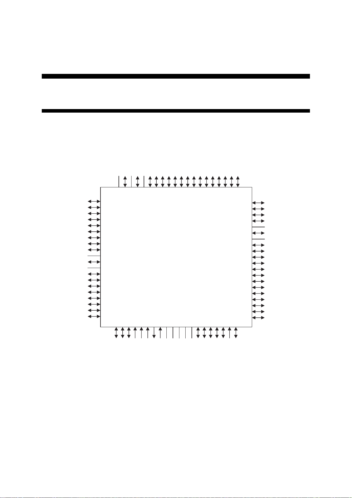
1.3 Pin Description
P
P
P
P
P
P
P
P
P
1
0
2
1
0
2
1
0
O
O
O
O
O
O
1.3.1 Pin Configuration
VDD2
P73/TM11IO
VSS
P72/TM11IO
VDD
P67/NPWM1
P66/PWM12
P65/NPWM1
P64/PWM11
P63/NPWM1
P62/PWM10
P57/NPWM0
P56/PWM02
P55/NPWM0
P54/PWM01
P53/NPWM0
P52/PWM00
P51/TM7IO
P47/TM10BI
Chapter 1
Overview
P46/TM10AI
P80/IRQ00
P81/IRQ01
P82/IRQ02
P83/IRQ03
TCPOUT
P90/ADIN00
P91/ADIN01
P92/ADIN02
P93/ADIN03
VSS
P94/ADIN04
P95/ADIN05
P96/ADIN06
P97/ADIN07
A0/ADIN08
A1/ADIN09
A2/ADIN10
A3/ADIN11
A4/ADIN12
VDD
80797877767574737271706968676665646362
1
2
3
4
5
6
7
8
9
10
11
12
13
14
15
16
17
18
19
20
80pinLQFP 0.65 pitch
MN103SA7D
MN103SA7G
MN103SFA7K
21222324252627282930313233343536373839
TEST1
TEST2
A5/ADIN13
A6/ADIN14
A7/ADIN15
OSCI
OSCO
TEST3
VSS
VDD
VDD3
VPPEX
VDD2
P10/IRQ04
P11/IRQ05
P12/IRQ06
P13/IRQ07
61
60
59
58
57
56
55
54
53
52
51
50
49
48
47
46
45
44
43
42
41
40
NRST
P14/IRQ08
16/TM17IO
P43/TM9BI
P42/TM9AI
P37/TM8BI
P36/TM8AI
VSS
P35/TM5IO
VDD
P34/TM4IO
P33/TM3IO
P32/TM2IO
P31/TM1IO
P27/SBI0
P26/SBT0
P25/SBO0
P24/SBI1
P23/SBT1
P22/SBO1
P21/SBI2
P20/SBT2
P17/SBO2
Figure:1.3.1 Pin Configuration
Pin Description I - 9

Chapter 1
Overview
1.3.2 Pin Specification
Table:1.3.1 Pin Specification
Pin
NRST - in - - Reset input
P10
P11
P12
P13
P14
P16
P17
P20
P21
P22
P23
P24
P25
P26
P27
P31
P32
P33
P34
P35
P36
P37
P42
P43
P46
P47
P51
P52
P53
P54
P55
P56
P57
P62
P63
P64
P65
P66
P67
P72
P73
P80
P81
P82
P83
P90
P91
P92
P93
P94
P95
P96
P97
Special
functions
IRQ04
IRQ05
IRQ06
IRQ07
IRQ08
TM17IO
SBO2
SBT2
SBI2
SBO1
SBT1
SBI1
SBO0
SBT0
SBI0
TM1IO
TM2IO
TM3IO
TM4IO
TM5IO
TM8AIO
TM8BIO
TM9AIO
TM9BIO
TM10AIO
TM10BIO
TM7IO
PWM00
NPWM00
PWM01
NPWM01
PWM02
NPWM02
PWM10
NPWM10
PWM11
NPWM11
PWM12
NPWM12
TM11IO0
TM11IO1
IRQ00
IRQ01
IRQ02
IRQ03
ADIN00
ADIN01
ADIN02
ADIN03
ADIN04
ADIN05
ADIN06
ADIN07
I/O
in/out
in/out
in/out
in/out
in/out
in/out
in/out
in/out
in/out
in/out
in/out
in/out
in/out
in/out
in/out
in/out
in/out
in/out
in/out
in/out
in/out
in/out
in/out
in/out
in/out
in/out
in/out
in/out
in/out
in/out
in/out
in/out
in/out
in/out
in/out
in/out
in/out
in/out
in/out
in/out
in/out
in/out
in/out
in/out
in/out
in/out
in/out
in/out
in/out
in/out
in/out
in/out
in/out
Direction
control
P10D
P11D
P12D
P13D
P14D
P16D
P17D
P20D
P21D
P22D
P23D
P24D
P25D
P26D
P27D
P31D
P32D
P33D
P34D
P35D
P36D
P37D
P42D
P43D
P46D
P47D
P51D
P52D
P53D
P54D
P55D
P56D
P57D
P62D
P63D
P64D
P65D
P66D
P67D
P72D
P73D
P80D
P81D
P82D
P83D
P90D
P91D
P92D
P93D
P94D
P95D
P96D
P97D
Pin
control
P10R
P11R
P12R
P13R
P14R
P16R
P17R
P20R
P21R
P22R
P23R
P24R
P25R
P26R
P27R
P31R
P32R
P33R
P34R
P35R
P36R
P37R
P42R
P43R
P46R
P47R
P51R
P52R
P53R
P54R
P55R
P56R
P57R
P62R
P63R
P64R
P65R
P66R
P67R
P72R
P73R
P80R
P81R
P82R
P83R
P90R
P91R
P92R
P93R
P94R
P95R
P96R
P97R
External interrupt input 4
External interrupt input 5
External interrupt input 6
External interrupt input 7
External interrupt input 8
Timer 17 input / output
Serial 2 transmission data output
Serial 2 clock I/O
Serial 2 reception data input
Serial 1 transmission data output
Serial 1 clock I/O
Serial 1 reception data input
Serial 0 transmission data output
Serial 0 clock I/O
Serial 0 reception data input
Timer 1 I/O
Timer 2 I/O
Timer 3 I/O
Timer 4 I/O
Timer 5 I/O
Timer 8A I/O
Timer 8B I/O
Timer 9A I/O
Timer 9B I/O
Timer 10A I/O
Timer 10B I/O
Timer 7 I/O
3-phase PWM0 signal output 0
3-phase PWM0 signal reverse output 0
3-phase PWM0 signal output 1
3-phase PWM0 signal reverse output 1
3-phase PWM0 signal output 2
3-phase PWM0 signal reverse output 2
3-phase PWM1 signal output 0
3-phase PWM1 signal reverse output 0
3-phase PWM1 signal output 1
3-phase PWM1 signal reverse output 1
3-phase PWM1 signal output 2
3-phase PWM1 signal reverse output 2
Timer 11 I/O 0
Timer 11 I/O 1
External interrupt input 0
External interrupt input 1
External interrupt input 2
External interrupt input 3
AD analog signal input 0
AD analog signal input 1
AD analog signal input 2
AD analog signal input 3
AD analog signal input 4
AD analog signal input 5
AD analog signal input 6
AD analog signal input 7
Function description
I - 10 Pin Description
 Loading...