

Page 1

MICROCOMPUTER MN103S
MN103S65G
LSI Application Note Excerption
Pub.No.3326501-010E
Page 2

PanaXSeries is a trademark of Matsushita Electric Industrial Co., Ltd.
The other corporation names, logotype and product names written in this book are trademarks or registered trademarks of their
corresponding corporations.
Request for your special attention and precautions in using the technical information
and semiconductors described in this book
(1) An export permit needs to be obtained from the competent authorities of the Japanese Government if any of
the products or technologies described in this book and controlled under the "Foreign Exchange and Foreign
Trade Law" is to be exported or taken out of Japan.
(2) The technical information described in this book is limited to showing representative characteristics and
applied circuits examples of the products. It neither warrants non-infringement of intellectual property right
or any other rights owned by our company or a third party, nor grants any license.
(3) W e are not liable for the infringement of rights owned by a third party arising out of the use of the product or
technologies as described in this book.
(4) The products described in this book are intended to be used for standard applications or general electronic
equipment (such as office equipment, communications equipment, measuring instrument s and household
appliances).
Consult our sales staff in advance for information on the following applications:
• Special applications (such as for airplanes, aerospace, automobiles, traffic control equipment, combustion
equipment, life support systems and safety devices) in which exceptional quality and reliability are required,
or if the failure or malfunction of the products may directly jeopardize life or harm the human body.
• Any applications other than the standard applications intended.
(5) The products and product specifications described in this book are subject to change without notice for
modification and/or improvement. At the final stage of your design, purchasing, or use of the prod ucts,
therefore, ask for the most up-to-date Product Standards in advance to make sure that the latest specifications
satisfy your requirements.
(6) When designing your equipment, comply with the guaranteed values, in particular those of maximum rating,
the range of operating power supply volta ge, and heat radiation characteristics. Otherwise, we will not be
liable for any defect which may arise later in your equipment.
Even when the products are used within the guaranteed values, take into the consideration of incidence of
break down and failure mode, possible to occur to semiconductor products. Measures on the systems such as
redundant design, arresting the spread of fire or preventing glitch are recommended in order to prevent
physical injury, fire, social damages, for example, by using the products.
(7) When using products for which damp-proof packing is required, observe the conditions (including shelf life
and amount of time let standing of unsealed items) agreed upon when specification sheets are individually
exchanged.
(8) This book may be not reprinted or reproduced whether wholly or partially, without the prior written
permission of Matsushita Electric Industrial Co., Ltd.
If you have any inquiries or questions about this book or our semiconductors, please contact one of our sales
offices listed at the back of this book.
Page 3
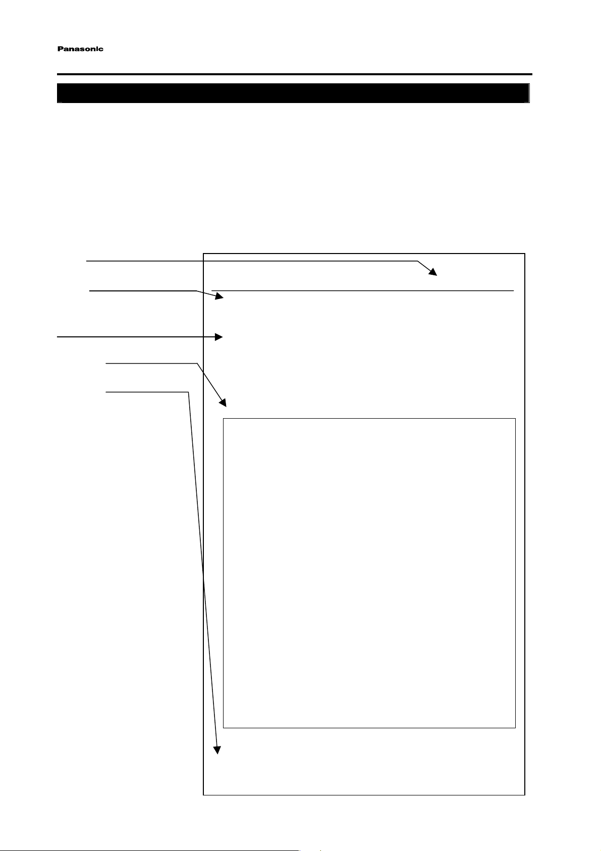
Table of Contents
About This Manual
■
Composition of this book
This LSI application note explains in order of the sample program which used the program collection which uses the
circumference circuit of MN103S65G loading, and 3-phase PWM.
■Composition as a manual
This book is roughly divided and consists of a title, the text, a sample program, an inclusion directory, cautions
information, and reference information.
Next, the layout and definition of each portion are shown.
1.Inside title
2.Small title
It is the minimum block of this book.
3.Text
4.Sample program
5.Inclusion directory
The inclusion directory is shown although
the sample program is recorded on
CD-ROM.
The example of this page is a
thing for explanation. It differs
from an actual page.
2-7 Port0
A port 0 is general-purpose 8-bit input/output port, and can set up input and output per bit.
a port 0 -- input and output -- also in which setup, addition of a pull-up resistor is possible
Moreover, it can be used as a terminal of the serial communication 0 and the serial communication 1 as a special
function.
The bit 0-2 is made to serve a double purpose as an input-and-output terminal of the serial communication 0.
The bit 3-5 is made to serve a double purpose as an input-and-output terminal of the serial communication 2.
A bit 6-7 can be used as an input-and-output terminal as it is.
When using serial communication, a serial output signal terminal is set as an "output."
It is [ following ] a sample program.
/* Declaration of control data When using the serial communication 0,
the serial communication 0 carries out a UART setup and a clock for monitors,
and it is an output setup. Other bits are input-set up. */
#define p0port 0x05 /* 0b00000101 Serial output Other inputs */
#define p0pulup 0x00 /* 0b00000000 A pull-up is not carried out for all.*/
/* Declaration of control data When using serial ports 0 and 2,
the serial communication 0 carries out a UART setup and a clock for monitors,
and it is an output setup.
The serial communication 2 is synchronous system and a slave setup.
Other bits are input-set up. */
#define p0port 0x0D /* 0b00001101 Bit0(CH0S),2(CH0CK),3(CH2S) */
#define p0pulup 0x00 /* 0b00000000 A pull-up is not carried out for all.*/
/* Declaration of the register address*/
#define P0OUT_adr 0x3F10
#define P0OUT (*(volatile unsigned char *)P0OUT_adr)
#define P0IN_adr 0x3F20
#define P0IN (*(volatile unsigned char *)P0IN_adr)
#define P0DIR_adr 0x3F30
#define P0DIR (*(volatile unsigned char *)P0DIR_adr)
#define P0PLU_adr 0x3F40
#define P0PLU (*(volatile unsigned char *)P0PLU_adr)
/* Setting program*/
P0DIR = p0port;
P0PLU = p0pulup;
This sample is recorded on CD-ROM.
Inclusion directory:SAMPLE\INITIAL\ASM\IOPORT\PORT0\
Inclusion directory:SAMPLE\INITIAL\C\IOPORT\PORT0\
Panasonic
2-7 Input and output, a peripheral initial
IV
Page 4

Table of Contents
Chapter1 Power supply injection
(power-onboot)Initialization of
the memory at the time
Chapter2 Each peripheral initial by C
Chapter3 The sample program in a
sample circuit
1
2
3
Chapter4 Appendix
4
VII
Page 5

Table of Contents
Chapter1 Initialization of the memory at the time of a power supply injection
(power-on boot)
Chapter2 Each peripheral initial by C
2-1 About description of C and an assembler............................................................................................................2-2
2-2 Interruption, a peripheral initial............................................................................................................................2-4
2-2-1 Interruption control register......................................................................................................................2-4
2-2-2 Interruption level (multiplex interruption)...............................................................................................2-6
2-3 The Interruption Processing Method................................................................................................................. 2-7
2-3-1 Interrupt vector table
2-3-2 Interruption group handler routine..................................................................................................... 2-7
2-3-3 Interruption processing program........................................................................................................ 2-7
2-3-4 The check of interruption................................................................................................................... 2-7
2-4 A 8-bit 16-bit timer, a peripheral initial ...............................................................................................................2-30
2-4-1 The various registers of a 8-bit timer.......................................................................................................2-30
2-4-2 The various registers of a 16-bit timer.....................................................................................................2-40
2-5 Serial communication, a peripheral initial...........................................................................................................2-51
2-5-1 The various registers of serial communication (channels 0 and 1)........................................................2-51
2-5-2 The various registers of serial communication (channel 2)....................................................................2-53
2-6 PWM for motor control........................................................................................................................................2-63
2-7 The initial of I/O Port ........................................................................................................................................ 2-70
2-7-1 Port0 ..........................................................................................................................................................2-71
2-7-2 Port1 ..........................................................................................................................................................2-71
2-7-3 Port2 ..........................................................................................................................................................2-72
2-7-4 Port3 ..........................................................................................................................................................2-73
2-7-5 Port4 ..........................................................................................................................................................2-74
2-7-6 Port5 ..........................................................................................................................................................2-75
2-7-7 Port6 ..........................................................................................................................................................2-76
2-7-8 Port7 ..........................................................................................................................................................2-77
2-7-9 Port8 ..........................................................................................................................................................2-78
2-7-10 Port9 ........................................................................................................................................................2-79
2-8 Noise filter function ................................................................................................................................................2-87
2-9 A/D conversion, a peripheral initial....................................................................................................................... 2-91
2-9-1 The various registers of A/D conversion.................................................................................................2-91
.......................................................................................................................... 2-7
VIII
Page 6

Table of Contents
Chapter 3 The sample program in a sample circuit
3-1 The outline of a sample circuit............................................................................................................................. 3-2
3-2 Composition of a sample program...................................................................................................................... 3-2
3-2-1 Sample program specification ................................................................................................................. 3-2
3-2-2 Composition of a sample program.......................................................................................................... 3-2
3-3 The set point about each processing in a sample program, and its explanation ...............................................3-3
3-3-1 Interruption processing (others [ - / external interruption and timer serial ])........................................ 3-3
3-3-2 Timer processing ...................................................................................................................................... 3-4
3-3-3 Processing about input/output port.......................................................................................................... 3-4
Chapter4 Appendix
4-1 Flash microcomputer............................................................................................................................................4-2
4-2 Purpose-oriented initialization............................................................................................................................. 4-3
4-3 Such at the time ....................................................................................................................................................4-4
4-4 About use of MAKE............................................................................................................................................ 4-6
4-5 The notes on circuitry........................................................................................................................................... 4-7
4-5-1 About supply voltage ............................................................................................................................... 4-7
4-5-2 About an analog input terminal............................................................................................................... 4-7
4-6 The notes on program creation............................................................................................................................ 4-7
4-6-1 Memory space.......................................................................................................................................... 4-7
4-7 The usage of C compiler...................................................................................................................................... 4-8
4-8 Class figure ........................................................................................................................................................... 4-10
4-9 Reference circuit diagram.................................................................................................................................... 4-11
IX
Page 7

2-4 A 8-bit 16-bit timer, a peripheral initial
2-4 A 8-bit 16-bit timer, a peripheral initial
2-4-1 The various registers of a 8-bit timer
Book LSI contains eight 8-bit timers, and is an interval timer, an event timer counter, and a clock output. It
can be used as the standard clock of a serial interface, and start timing of A/D conversion.
These timers can perform cascade connection use of a maximum of four.
●Timer register
It is the 8-bit register which counts a timer. A count value can be read by the down counter.
TM0BC,TM1BC,TM3BC,TM4BC,TM5BC,TM6BC,TM7BC
●Timer mode register
It is the 8-bit register which sets up the mode of a timer of operation.
The clock source which can be chosen by each timer is different. Be careful of a setup.
TM0D: Timer 0 mode register
Bit7 : Count operation permission
0: A stop of operation
1: Permission of operation
Bit6 : Base register setup
0: Usually, operation
1: Initialization
The value of a base register is loaded to a binary counter.
The timer pulse output 0 is reset on a low level.
Bit5-3: Prohibition (0 fixation)
Bit2-0: Clock source selection
000:IOCLK
001:IOCLK/8
010:IOCLK/32
011: Prohibition of a setup
100: Prohibition of a setup
101: Timer 1 underflow
2-30
Page 8

2-4 A 8-bit 16-bit timer, a peripheral initial
110: Timer 1 underflow
111: TMIN0 terminal input
TM1MD: Timer 1 mode register
Bit7 : Count operation permission
0: A stop of operation
1: Permission of operation
Bit6 : Base register setup
0: Usually, operation
1: Initialization
The value of a base register is loaded to a binary counter.
The timer pulse output 1 is reset on a low level.
Prohibition (0 fixation)
Bit 2-0: Clock source selection
000:IOCLK
001:IOCLK/8
010:IOCLK/32
011: Cascade connection with a timer 0
100: Timer 0 underflow
101: Prohibition of a setup
110: Timer 2 underflow
111: TMIN1 terminal input
TM2MD: Timer 2 mode register
Bit7 : Timer operation permission
0: A stop of operation
1: Permission of operation
Bit6 : Timer initialization
0: Usually, operation
1: Initialization
The value of a base register is loaded to a binary counter.
The timer pulse output 2 is reset on a low level.
Bit 5-3: Prohibition (0 fixation)
Bit2-0: Clock source selection
000:IOCLK
001:IOCLK/8
010:IOCLK/32
011: Cascade connection with a timer 1
100: Timer 0 underflow
2-31
Page 9

2-4 A 8-bit 16-bit timer, a peripheral initial
101: Timer 1 underflow
110: Prohibition of a setup
111: TMIN2 terminal input
TM3MD: Timer 3 mode register
Bit7 : Timer operation permission
0: Stop of operation
1: Initialization
Bit6 : Timer initialization
0: Usually, operation
1: Initialization
The value of a base register is loaded to a binary counter.
The timer pulse output 3 is reset on a low level.
Bit5-3: Prohibition (0 fixation)
Bit2-0: Clock source selection
000:IOCLK
001:IOCLK/8
010:IOCLK/32
011: Cascade connection with a timer 2
100: Timer 0 underflow
101: Timer 1 underflow
110: Timer 0 underflow
111: TMIN3 terminal input
TM4MD: Timer 4 mode register
Bit7 : Timer operation permission
0: Stop of operation
1: Permission of operation
Bit6 : Timer initialization
0: Usually, operation
1: Initialization
The value of a base register is loaded to a binary counter.
The timer pulse output 4 is reset on a low level.
Bit5-3: Prohibition (0 fixation)
Bit2-0: Clock source selection
000:IOCLK
001:IOCLK/8
010:IOCLK/32
011: Prohibition of a setup
100: Prohibition of a setup
101: Timer 5 underflow
2-32
Page 10

2-4 A 8-bit 16-bit timer, a peripheral initial
110: Timer 6 underflow
111: TMIN4 terminal input
TM5MD: Timer 5 mode register
Bit7 : Timer operation permission
0: Stop of operation
1: Permission of operation
Bit6 : Timer initialization
0: Usually, operation
1: Initialization
The value of a base register is loaded to a binary counter.
The timer pulse output 5 is reset on a low level.
Bit5-3: Prohibition (0 fixation)
Bit2-0: Clock source selection
000:IOCLK
001:IOCLK/8
010:IOCLK/32
011: Cascade connection with a timer 4
100: Timer 4 underflow
101: Prohibition of a setup
110: Timer 6 underflow
111: TM5IN terminal input
TM6MD: Timer 6 mode register
Bit7 : Timer operation permission
0: Stop of operation
1: Permission of operation
Bit6 : Timer initialization
0: Usually, operation
1: Initialization
The value of a base register is loaded to a binary counter.
The timer pulse output 6 is reset on a low level.
Bit5-3: Prohibition (0 fixation)
Bit2-0: Clock source selection
000:IOCLK
001:IOCLK/8
010:IOCLK/32
011: Cascade connection with a timer 5
100: Timer 4 underflow
101: Timer 5 underflow
110: Prohibition of a setup
111: TM6IN terminal input
2-33
Page 11

2-4 A 8-bit 16-bit timer, a peripheral initial
TM7MD: Timer 7 mode register
Bit7 : Timer operation permission
0: Stop of operation
1: Permission of operation
Bit6 : Timer initialization
0: Usually, operation
1: Initialization
The value of a base register is loaded to a binary counter.
The timer pulse output 7 is reset on a low level.
Bit5-3: Prohibition (0 fixation)
Bit2-0: Clock source selection
000:IOCLK
001:IOCLK/8
010:IOCLK/32
011: Cascade connection with a timer 6
100: Timer 4 underflow
101: Timer 5 underflow
110: Timer 6 underflow
111: TM7IN terminal input
TMMPSC: Prescaler mode register
Bit7 : Count operation permission
0: Stop of operation
1: Permission of operation
To use 1/8SYSCLK, and 1/32SYSCLK, a Prescaler control register needs to be set up.
When a TMnIO terminal input is chosen, the rising edge of a terminal input is counted.
TMEXPSC8: External Prescaler control register
Bit03-01: Count source selection (timers 0, 2, and 4)
0:TMINn terminal input
1:IOCLK/128
Bit00 : Prescaler (1 / 128 operation permission)
0: Stop of operation
1: Permission of operation
2-34
Page 12

2-4 A 8-bit 16-bit timer, a peripheral initial
●Various setup of a 8-bit timer
It is a setup when using it as an interval timer.
/*******************************
* Register address
*******************************/
/* Timer 0 register address declaration */
#define TM0BC (*((volatile unsigned char *)0x0000A150))
#define TM0BR (*((volatile unsigned char *)0x0000A148))
#define TM0MD (*((volatile unsigned char *)0x0000A140))
/* Timer 1 register address declaration */
#define TM1BC (*((volatile unsigned char *)0x0000A151))
#define TM1BR (*((volatile unsigned char *)0x0000A149))
#define TM1MD (*((volatile unsigned char *)0x0000A141))
/* Timer 2 register address declaration */
#define TM2BC (*((volatile unsigned char *)0x0000A154))
#define TM2BR (*((volatile unsigned char *)0x0000A14C))
#define TM2MD (*((volatile unsigned char *)0x0000A144))
/* Timer 3 register address declaration */
#define TM3BC (*((volatile unsigned char *)0x0000A155))
#define TM3BR (*((volatile unsigned char *)0x0000A14D))
#define TM3MD (*((volatile unsigned char *)0x0000A145))
/* Timer 4 register address declaration */
#define TM4BC (*((volatile unsigned char *)0x0000A170))
#define TM4BR (*((volatile unsigned char *)0x0000A168))
#define TM4MD (*((volatile unsigned char *)0x0000A160))
/* Timer 5 register address declaration */
#define TM5BC (*((volatile unsigned char *)0x0000A171))
#define TM5BR (*((volatile unsigned char *)0x0000A169))
#define TM5MD (*((volatile unsigned char *)0x0000A161))
/* Timer 6 register address declaration */
#define TM6BC (*((volatile unsigned char *)0x0000A174))
#define TM6BR (*((volatile unsigned char *)0x0000A16C))
#define TM6MD (*((volatile unsigned char *)0x0000A164))
/* Timer 7 register address declaration */
#define TM7BC (*((volatile unsigned char *)0x0000A175))
#define TM7BR (*((volatile unsigned char *)0x0000A16D))
#define TM7MD (*((volatile unsigned char *)0x0000A165))
/* Pre-scaler register address declaration */
/* timer 0-3 */
#define TM03PSC (*((volatile unsigned char *)0x0000A158))
/* timer 4-7 */
#define TM47PSC (*((volatile unsigned char *)0x0000A178))
/* pre-scaler control register*/
#define TMEXPSC8 (*((volatile unsigned char *)0x0000A17C))
/* Declaration of setting data */
#define TM0MD_STOP 0x00 /* timer stop */
2-35
Page 13

2-4 A 8-bit 16-bit timer, a peripheral initial
#define TM0_COUNT4 3 /* cycles/min ratio setup (4 cycles/min -1) */
#define TM0MD_LOAD1 0x07 /* TMIN0 Terminal input setup */
#define TM0MD_STABLE1 0x00 /* stabilization */
#define TM0MD_START1 0x40 /* timer start */
#define TM0MD_ENABLE1 0x80 /* timer permission*/
#define PS0MD_STOP 0x00 /* pre-scaler stop */
#define PS0MD_START 0x80 /* pre-scaler start*/
#define TM1MD_STOP 0x00 /* timer stop*/
#define TM1_COUNT3 5 /* cycles/min ratio setup (5 cycles/min -1) */
#define TM1MD_LOAD1 0x03 /* load cycles/min ratio*/
#define TM1MD_STABLE1 0x00 /* stabilization */
#define TM1MD_START1 0x40 /* timer start */
#define TM1MD_ENABLE1 0x80 /* timer permission*/
#define PS0_COUNT200 199 /* cycles/min setup (200 cycles/min-1) */
#define TM0_COUNT0x5f 0x5f /* cycles/min setup (0xea5f = 0xea60(60000) - 1) */
#define TM1_COUNT0xea 0xea /* cycles/min setup (0xea5f = 0xea60(60000) - 1) */
#define TM0MD_LOAD2 0x42 /* read cycles/min ratio */
/* clock source (pre-scaler 0 clock ) setup */
#define TM1MD_LOAD2 0x03 /* timer 0 and cascade connection*/
#define TM0MD_STABLE2 0x02 /* stabilization*/
#define TM1MD_STABLE2 0x01 /* stabilization*/
#define TM0MD_START2 0x82 /* timer start*/
#define TM1MD_START2 0x81 /* timer start */
/***********************************************
* Interval timer by 8-bit timer
* Pre-scaler 0 is used, and the cascade connection of the timers 0
* and 1 is carried out, and it is used as a 16-bit timer.
***********************************************/
void initInterval8( void )
{
unsigned short data0,data1;
TM03PSC = PS0MD_STOP; /* pre-scaler stop*/
TM0MD = TM0MD_STOP; /* timer stop*/
TM1MD = TM1MD_STOP; /* timer stop*/
/* Setup of timer cycles/min ratio 60000-1 */
TM0BR = TM0_COUNT0x5f; /* cycles/min setup 0xea5f=59999 */
TM1BR = TM1_COUNT0xea; /* cycles/min setup*/
data0 = 0;
TM0MD = data0; /* Arbitrary setup */
data1 = TM1MD_LOAD2;
TM1MD = data1; /* timer 0 and cascade setup */
data0 |= TM0MD_START1;
TM0MD = data0; /* Timer 0 initialization LDE=1 */
data1 |= TM1MD_START1;
TM1MD = data1; /* Timer 1 initialization LDE=1 */
data0 &= ~TM0MD_START1;
TM0MD = data0; /* Timer 0 start LDE=0 */
2-36
Page 14

2-4 A 8-bit 16-bit timer, a peripheral initial
data1 &= ~TM1MD_START1;
TM1MD = data1; /* Timer 1 start LDE=0 */
data1 |= TM1MD_ENABLE1;
TM1MD = data1; /* Timer 1 permission CNE=1 */
data0 |= TM0MD_ENABLE1;
TM0MD = data0; /* Timer 0 permission CNE=1 */
TM03PSC = PS0MD_START; /* Pre-scaler start */
TM0MD = TM0MD_START2; /* Timer start*/
TM1MD = TM1MD_START2; /* Timer start */
}
The sample of a 8-bit timer is recorded on attached CD-ROM.
Inclusion director:program\initial\timecounter\timer8\
program :timer8int.c
It is a setup when using it as an event timer.
/*******************************
* Register address
*******************************/
/* Timer 0 register address declaration */
#define TM0BC (*((volatile unsigned char *)0x0000A150))
#define TM0BR (*((volatile unsigned char *)0x0000A148))
#define TM0MD (*((volatile unsigned char *)0x0000A140))
/* Timer 1 register address declaration */
#define TM1BC (*((volatile unsigned char *)0x0000A151))
#define TM1BR (*((volatile unsigned char *)0x0000A149))
#define TM1MD (*((volatile unsigned char *)0x0000A141))
/* Timer 2 register address declaration */
#define TM2BC (*((volatile unsigned char *)0x0000A154))
#define TM2BR (*((volatile unsigned char *)0x0000A14C))
#define TM2MD (*((volatile unsigned char *)0x0000A144))
/* Timer 3 register address declaration */
#define TM3BC (*((volatile unsigned char *)0x0000A155))
#define TM3BR (*((volatile unsigned char *)0x0000A14D))
#define TM3MD (*((volatile unsigned char *)0x0000A145))
/* Timer 4 register address declaration */
#define TM4BC (*((volatile unsigned char *)0x0000A170))
#define TM4BR (*((volatile unsigned char *)0x0000A168))
#define TM4MD (*((volatile unsigned char *)0x0000A160))
/* Timer 5 register address declaration */
#define TM5BC (*((volatile unsigned char *)0x0000A171))
#define TM5BR (*((volatile unsigned char *)0x0000A169))
#define TM5MD (*((volatile unsigned char *)0x0000A161))
/* Timer 6 register address declaration */
#define TM6BC (*((volatile unsigned char *)0x0000A174))
#define TM6BR (*((volatile unsigned char *)0x0000A16C))
#define TM6MD (*((volatile unsigned char *)0x0000A164))
2-37
Page 15

2-4 A 8-bit 16-bit timer, a peripheral initial
/* Timer 7 register address declaration */
#define TM7BC (*((volatile unsigned char *)0x0000A175))
#define TM7BR (*((volatile unsigned char *)0x0000A16D))
#define TM7MD (*((volatile unsigned char *)0x0000A165))
/* Pre-scaler register address declaration */
/* timer 0-3 */
#define TM03PSC (*((volatile unsigned char *)0x0000A158))
/* timer 4-7 */
#define TM47PSC (*((volatile unsigned char *)0x0000A178))
/* Pre-scaler control register */
#define TMEXPSC8 (*((volatile unsigned char *)0x0000A17C))
/* Declaration of setting data */
#define TM0MD_STOP 0x00 /* Timer stop*/
#define TM0_COUNT4 3 /* cycles/min ratio setup (4 cycles/min-1) */
#define TM0MD_LOAD1 0x07 /* TMIN0 Terminal input setup */
#define TM0MD_STABLE1 0x00 /* Stabilization */
#define TM0MD_START1 0x40 /* timer start*/
#define TM0MD_ENABLE1 0x80 /* Timer permission */
#define PS0MD_STOP 0x00 /* Pre-scaler stop*/
#define PS0MD_START 0x80 /* Pre-scaler start*/
#define TM1MD_STOP 0x00 /* timer stop*/
#define TM1_COUNT3 5 /* cycles/min ratio setup(5 cycles/min-1) */
#define TM1MD_LOAD1 0x03 /* cycles/min ratio reloaded */
#define TM1MD_STABLE1 0x00 /* stabilization*/
#define TM1MD_START1 0x40 /* timer start*/
#define TM1MD_ENABLE1 0x80 /* timer permission */
#define PS0_COUNT200 199 /* cycles/min ratio setup (200 cycles/min-1) */
#define TM0_COUNT0x5f 0x5f /* cycles/min ratio setup (0xea5f = 0xea60(60000) - 1) */
#define TM1_COUNT0xea 0xea /* cycles/min ratio setup (0xea5f = 0xea60(60000) - 1) */
#define TM0MD_LOAD2 0x42 /* cycles/min ratio reloaded */
/* Clock source (Pre-scaler 0 clock) setup*/
#define TM1MD_LOAD2 0x03 /* timer 0 and cascade connection */
#define TM0MD_STABLE2 0x02 /* stabilization */
#define TM1MD_STABLE2 0x01 /* stabilization */
#define TM0MD_START2 0x82 /* timer start */
#define TM1MD_START2 0x81 /* timer start */
/***********************************************
* Event counter by 8-bit timer
* TMIN0 terminal is carried out for 1 / 4 cycles/min using a timer 0,
* and underflow interruption is generated.
***********************************************/
void initEventCounter8( void )
{
unsigned short data;
data = TM0MD_STOP;
TM0MD = data; /* timer stop */
/* TM0 underflow interruption is permitted. */
2-38
Page 16

2-4 A 8-bit 16-bit timer, a peripheral initial
/* A port 0 is set as TM0IO (input). */
TM0BR = TM0_COUNT4; /* cycles/min ratio setup */
data |= TM0MD_LOAD1;
TM0MD = data; /* count source setup input TMIN0*/
data |= TM0MD_START1;
TM0MD = data; /* initialize timer LDE=1 */
data &= ~TM0MD_START1;
TM0MD = data; /* Timer start LDE=0 */
data |= TM0MD_ENABLE1;
TM0MD = data; /* Timer permission CNE=1 */
}
The sample of a 8-bit timer is recorded on attached CD-ROM.
Inclusion directory:program\initial\timecounter\timer8\
program :timer8evt.c
2-39
Page 17

MN103S65G
LSI Application Note Excerption
March, 2004 1st Edition
Issued by Matsushita Electric Industrial Co., Ltd.
Matsushita Electric Industrial Co., Ltd.
Page 18

SALES OFFICES
NORTH AMERICA
˜ U.S.A. Sales Office:
Panasonic Industrial Company [PIC]
— New Jersey Office:
2 Panasonic Way Secaucus, New Jersey 07094, U.S.A.
— Chicago Office:
1707 N. Randall Road Elgin, Illinois 60123-7847, U.S.A.
— San Jose Office:
2033 Gateway Place, Suite 200, San Jose, California 95110,
U.S.A
— Atlanta Office:
1225 Northbrook Parkway Suite 1-151 Suwanee, Georgia 30024,
U.S.A.
— San Diego Office:
9444 Balboa Avenue, Suite 185, San Diego, California 92123,
U.S.A.
˜
Panasonic Canada Inc. [PCI]
5770 Ambler Drive 27 Mississauga, Ontario L4W 2T3, Canada
Tel:1-201-348-5257 Fax:1-201-392-4652
Tel:1-847-468-5720 Fax:1-847-468-5725
Tel:1-408-487-9510 Fax:1-408-436-8037
Tel:1-770-338-6953 Fax:1-770-338-6849
Tel:1-858-503-2910 Fax:1-858-715-5545
Canada Sales Office:
Tel:1-905-238-2243 Fax:1-905-238-2414
LATIN AMERICA
˜ Mexico Sales Office:
Panasonic de Mexico, S.A. de C.V. [PANAMEX]
Amores 1120 Col. Del Valle Delegacion Benito Juarez C.P. 03100
Mexico, D.F. Mexico
— Guadalajara Office:
Sucursal Guadarajara Av. Lazaro Cardenas 2305 Local G-102
Plaza Comercial Abastos; Col. Las Torres Guadalajara, Jal.
44920, Mexico
˜ Brazil Sales Office:
Panasonic do Brasil Ltda. [PANABRAS]
Caixa Postal 1641, Sao Jose dos Campos, Estado de Sao Paulo,
Brasil
Tel:52-5-488-1000 Fax:52-5-488-1073
Tel:52-3-671-1205 Fax:52-3-671-1256
Tel:55-12-3935-9000 Fax:55-12-3931-3789
EUROPE
˜ Europe Sales Office:
Panasonic Industrial Europe GmbH [PIE]
— Germany Sales Office:
Hans-Pinsel-Strasse 2 85540 Haar, Germany
Tel:49-89-46159-119 Fax:49-89-46159-195
ASIA
˜
Singapore Sales Office:
Panasonic Semiconductor of South Asia [PSSA]
300 Beach Road, #16-01, the Concourse, Singapore 199555, the
Republic of Singapore
˜
Malaysia Sales Office:
Panasonic Industrial Company (M) Sdn. Bhd. [PICM]
— Head Office:
15th Floor, Menara IGB, Mid Valley City, Lingkaran Syed
Putra, 59200 Kuala Lumpur, Malaysia
— Penang Office:
Suite 20-07,20th Floor, MWE Plaza, No.8, Lebuh Farquhar,10200
Penang, Malaysia
— Johore Sales Office:
Menara Pelangi, Suite8.3A, Level8, No.2, Jalan Kuning, Taman
Pelangi, 80400 Johor Bahru, Johor, Malaysia
˜
Thailand Sales Office:
Panasonic Industrial (Thailand) Ltd. [PICT]
252-133 Muang Thai-Phatra Complex Building, 31st Floor
Rachadaphisek Road, Huaykwang, Bangkok 10320, Thailand
˜
Philippines Sales Office:
Panasonic Industrial Sales Philippines [PISP]
102 Laguna Boulevard,Bo.Don Jose Laguna Technopark, Santa.
Rosa, Laguna 4026, the Philippines
˜
China Sales Office:
Panasonic Industrial (Shanghai) Co., Ltd. [PI(SH)]
Floor 12, China Insurance Building, 166 East Road
Lujiazui, Pudong New District, Shanghai 200120, China
Panasonic Industrial (Tianjin) Co., Ltd. [PI(TJ)]
Room No.1001, Tianjin International Building 75, Nanjin Road,
Tianjin 300050, China
Panasonic SH Industrial Sales (Shenzhen) Co., Ltd.[PSI(SZ)]
— Shum Yip Centre Office:
25F, Shum Yip Centre, #5045, East Shennan Road, Shenzhen,
China
Panasonic Shun Hing Industrial Sales (Hong Kong)
[PSI(HK)]
11th Floor, Great Eagle Center 23 Harbour Road, Wanchai, Hong
Kong
˜
Taiwan Sales Office:
Panasonic Industrial Sales (Taiwan) Co.,Ltd. [PIST]
— Head Office:
6F, 550, Sec. 4, Chung Hsiao E. RD. Taipei 110, Taiwan
— Kaohsiung Office:
6th Floor, Hsin Kong Bldg. No.251, Chi Hsien 1st Road,
Kaohsiung 800, Taiwan
˜
Korea Sales Office:
Panasonic Industrial Korea Co., Ltd. [PIKL]
Kukje Center Bldg. 11th Floor, 191 Hangangro 2ga, Youngsan-ku,
Seoul 140-702, Korea
Tel:65-6390-3688 Fax:65-6390-3689
Tel:60-3-2297-6888 Fax:60-6-2284-6898
Tel: 60-4-201-5113 Fax:60-4-261-9989
Tel:60-7-331-3822 Fax:60-7-355-3996
Tel:66-2-693-3400 to 3421 Fax:66-2-693-3422 to 3427
Tel:63-2-520-8615 Fax:63-2-520-8629
Tel:86-21-6841-9642 Fax:86-21-6841-9631
Tel:86-22-2313-9771 Fax:86-22-2313-9770
Tel:86-755-8211-0888 Fax:86-755-8211-0970
Co., Ltd.
Tel:852-2529-7322 Fax:852-2865-3697
Tel:886-2-2757-1900 Fax:886-2-2757-1906
Tel:886-7-346-3815 Fax:886-7-236-8362
Tel:82-2-795-9600 Fax:82-2-795-1542
Semiconductor Company, Matsushita Electric Industrial Co., Ltd.
Nagaokakyo, Kyoto 617-8520, Japan
Tel:075-951-8151
http://panasonic.co.jp/semicon/e-index.html
050204 Printed in Japan
 Loading...