

Panasonic F77G, MN101C77C User Manual

MICROCOMPUTER MN101C
MN101C77C/F77G
LSI User ’s Manual
Pub.No.21477-011E


PanaXSeries is a trademark of Matsushita Electric Industrial Co., Ltd.
The other corporation names, logotype and product names written in this book are trademarks or registered trademarks of their
corresponding corporations.
Request for your special attention and precautions in using the technical information
and semiconductors described in this book
(1) An export permit needs to be obtained from the competent authorities of the Japanese Government if any of
the products or technologies described in this book and controlled under the "Foreign Exchange and Foreign
Trade Law" is to be exported or taken out of Japan.
(2) The technical information described in this book is limited to showing representative characteristics and
applied circuits examples of the products. It neither warrants non-infringement of intellectual property right
or any other rights owned by our company or a third party, nor grants any license.
(3) W e are not liable for the infringement of rights owned by a third party arising out of the use of the product or
technologies as described in this book.
(4) The products described in this book are intended to be used for standard applications or general electronic
equipment (such as office equipment, communications equipment, measuring instrument s and household
appliances).
Consult our sales staff in advance for information on the following applications:
• Special applications (such as for airplanes, aerospace, automobiles, traffic control equipment, combustion
equipment, life support systems and safety devices) in which exceptional quality and reliability are required,
or if the failure or malfunction of the products may directly jeopardize life or harm the human body.
• Any applications other than the standard applications intended.
(5) The products and product specifications described in this book are subject to change without notice for
modification and/or improvement. At the final stage of your design, purchasing, or use of the prod ucts,
therefore, ask for the most up-to-date Product Standards in advance to make sure that the latest specifications
satisfy your requirements.
(6) When designing your equipment, comply with the guaranteed values, in particular those of maximum rating,
the range of operating power supply volta ge, and heat radiation characteristics. Otherwise, we will not be
liable for any defect which may arise later in your equipment.
Even when the products are used within the guaranteed values, take into the consideration of incidence of
break down and failure mode, possible to occur to semiconductor products. Measures on the systems such as
redundant design, arresting the spread of fire or preventing glitch are recommended in order to prevent
physical injury, fire, social damages, for example, by using the products.
(7) When using products for which damp-proof packing is required, observe the conditions (including shelf life
and amount of time let standing of unsealed items) agreed upon when specification sheets are individually
exchanged.
(8) This book may be not reprinted or reproduced whether wholly or partially, without the prior written
permission of Matsushita Electric Industrial Co., Ltd.
If you have any inquiries or questions about this book or our semiconductors, please contact one of our sales
offices listed at the back of this book.
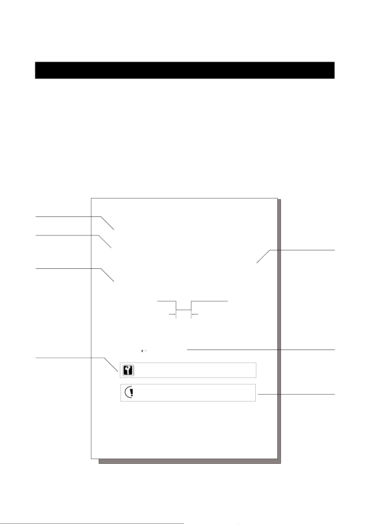
About This Manual
Organization
In this LSI manual, this LSI functions are presented in the following order : overview, basic CPU functions, interrupt
functions, port functions, timer functions, serial functions, and other peripheral hardware functions.
Each section contains overview of function, block diagram, control register, operation, and setting example.
Manual Configuration
Each section of this manual consists of a title, summary, main text, key information, precautions and warnings, and
references.
The layout and definition of each section are shown below.
Subtitle
Sub-subtitle
The smallest block
in this manual.
Main text
Key information
Important information
from the text.
Chapter 2 Basic CPU
2-8 Reset
2-8-1 Reset operation
The CPU contents are reset and registers are initialized when the NRST pin (P.27) is pulled to low.
Initiating a Reset
There are two methods to initiate a reset.
(1) Drive the NRST pin low for at least four clock cycles.
NRST pin should be holded "low" for more than 4 clock cycles (200 nS at a 20 MHz).
NRST pin
4 clock cycles
(200 nS at a 20 MHz)
Figure 2-8-1 Minimum Reset Pulse Width
(2) Setting the P2OUT7 flag of the P2OUT register to "0" outputs low level at P27 (NRST) pin. And
transfering to reset by program (software reset) can be executed. If the internal LSI is reset and
register is initiated, the P2OUT7 flag becomes "1" and reset is released.
[ Chapter 4. 4-4-2 Registers ]
On this LSI, the starting mode is NORMAL mode that high oscillation is the base clock.
When the power voltage low circuit is connected to NRST pin, circuit that gives pulse for
enough low level time at sudeen unconnected. And reset can be generated even if its pulse
is low level as the oscillation clock is under 4 clocks, take notice of noise.
Summary
Introduction to the
section.
References
References for the
main text.
Precautions and
warnings
Precautions are listed
in case.
Be sure to read these
of lost functionality or
damage.
About This Manual 1
II - 44
Reset

Finding Desired Information
This manual provides three methods for finding desired information quickly and easily.
(1) Consult the index at the front of the manual to locate the beginning of each section.
(2) Consult the table of contents at the front of the manual to locate desired titles.
(3) Chapter names are located at the top outer corner of each page, and section titles are located
at the bottom outer corner of each page.
Related Manuals
Note that the following related documents are available.
"MN101C Series LSI user's Manual"
<Describes the device hardware>
"MN101C Series Instruction Manual"
<Describes the instruction set.>
"MN101C Series C Compiler User's Manual: Usage Guide"
<Describes the installation, the commands, and options of the C Compiler.>
"MN101C Series C Compiler User's Manual: Language Description"
<Describes the syntax of the C Compiler.>
"MN101C Series C Compiler User's Manual: Library Reference"
<Describes the standard library of the C Compiler.>
"MN101C Series Cross-assembler User's Manual"
<Describes the assembler syntax and notation.>
"MN101C Series C Source Code Debugger User's Manual"
<Describes the use of C source code debugger.>
"MN101C Series PanaX Series Installation Manual"
<Describes the installation of C compiler, cross-assembler and C source code debugger
and the procedure for bringing up the in-circuit emulator.>
About This Manual 2


Chapter 1 Overview
1
Chapter 2 CPU Basics
Chapter 3 Interrupts
2
3
3
Chapter 4 I/O Ports
Chapter 5 Prescaler 5
Chapter 6 8-bit Timers
Chapter 7 16-bit Timer
Chapter 8 Time Base Timer /
8-bit Free-running Timer
4
6
7
8
11
2
Chapter 9 Watchdog Timer
Chapter 10 Buzzer
Chapter 11 Serial Interface 0,1
Chapter 12 Serial Interface 3
Chapter 13 Serial Interface 4
Chapter 14 Automatic Transfer
Controller
Chapter 15 A/D Converter
9
10
11
12
13
14
15
Chapter 16 D/A Converter
Chapter 17 Appendices
Chapter 18 Flash EEPROM
16
17
18

Contents
Chapter 1 Overview
1-1 Overview ..................................................................................................................... I - 2
1-1-1 Overview .................................................................................................... I - 2
1-1-2 Product Summary ....................................................................................... I - 2
1-2 Hardware Functions .................................................................................................... I - 3
1-3 Pin Description............................................................................................................ I - 9
1-3-1 Pin Configuration ....................................................................................... I - 9
1-3-2 Pin Specification....................................................................................... I - 10
1-3-3 Pin Functions ........................................................................................... I - 1 1
1- 4 Block Diagram ........................................................................................................... I - 17
1-4-1 Block Diagram .......................................................................................... I - 1 7
1- 5 Electrical Characteristics ........................................................................................... I - 18
1-5-1 Absolute Maximum Ratings ..................................................................... I - 18
1-5-2 Operating Conditions ............................................................................... I - 19
1-5-3 DC Characteristics .................................................................................... I - 22
1-5-4 A/D Converter Characteristics ................................................................. I - 26
1-5-5 D/A Converter Characteristics ................................................................. I - 27
1-6 Precautions................................................................................................................ I - 28
1-6-1 General Usage .......................................................................................... I - 28
1-6-2 Unused Pins ............................................................................................. I - 2 9
1-6-3 Power Supply ........................................................................................... I - 31
1-6-4 Power Supply Circuit................................................................................ I - 32
1-7 Package Dimension ................................................................................................... I - 33
Chapter 2 CPU Basics
2-1 Overview.................................................................................................................. II - 2
2-1-1 Block Diagram ....................................................................................... II - 3
2-1-2 CPU Control Registers ........................................................................... II - 4
2-1-3 Instruction Execution Controller ........................................................... II - 5
2-1-4 Pipeline Process...................................................................................... II - 6
2-1-5 Registers for Address.............................................................................. II - 6
2-1-6 Registers for Data ................................................................................... II - 7
2-1-7 Processor Status Word ............................................................................ II - 8
2-1-8 Addressing Modes ............................................................................... II - 10
2-2 Memory Space....................................................................................................... II - 12
2-2-1 Memory Mode ...................................................................................... II - 12
2-2-2 Single-chip Mode ................................................................................. II - 13
2-2-3 Special Function Registers...................................................................... II - 14
2-3 Bus Interface ............................................................................................................ II - 15
ii
contents

2-3-1 Bus Controller ......................................................................................... II - 15
2-3-2 Control Registers..................................................................................... II - 16
2-4 Standby Function..................................................................................................... II - 19
2-4-1 Overview ................................................................................................. II - 19
2-4-2 CPU Mode Control Register.................................................................... II - 2 1
2-4-3 Transition between SLOW and NORMAL.............................................. II - 22
2-4-4 Transition to ST ANDBY Modes ............................................................. II - 23
2- 5 Clock Switching........................................................................................................ II - 25
2-6 Bank Function .......................................................................................................... II - 27
2-6-1 Overview ................................................................................................. II - 27
2-6-2 Bank Setting ............................................................................................ II - 27
2-6-3 Bank Memory Space ............................................................................... II - 29
2- 7 ROM Correction ....................................................................................................... II - 30
2-7-1 Overview ................................................................................................. II - 30
2-7-2 Correction Sequence ............................................................................... II - 30
2-7-3 ROM Correction Control Register ........................................................... II - 32
2-7-4 ROM Correction Setup Example .............................................................. II - 35
2-8 Reset ........................................................................................................................ II - 38
2-8-1 Reset Operation....................................................................................... II - 38
2-8-2 Oscillation Stabilization W ait T ime.......................................................... II - 40
2-9 Register Protection................................................................................................... II - 42
2-9-1 Overview ................................................................................................. II - 42
2-9-2 Setting of the Register Protection Function ............................................ II - 4 2
2-9-3 Rewrite Procedure ................................................................................... II - 42
Chapter 3 Interrupts
3-1 Overview................................................................................................................. III - 2
3-1-1 Functions ............................................................................................... III - 3
3-1-2 Block Diagram ...................................................................................... III - 4
3-1-3 Operation ............................................................................................... III - 5
3-1-4 Interrupt Flag Setup............................................................................... III - 14
3-2 Control Registers.................................................................................................. III - 15
3-2-1 Registers List ....................................................................................... III - 15
3-2-2 Interrupt Control Registers.................................................................. III - 16
3-3 External Interrupts ................................................................................................... III - 38
3-3-1 Overview ................................................................................................ III - 38
3-3-2 Block Diagram ........................................................................................ III - 39
3-3-3 Control Registers.................................................................................... III - 42
3-3-4 Programmable Active Edge Interrupt ..................................................... III - 47
3-3-5 Both Edges Interrupt.............................................................................. III - 48
3-3-6 Key Input Interrupt ................................................................................ III - 19
3-3-7 Noise Filter ............................................................................................. III - 51
iii
contents

3-3-8 AC Zero-Cross Detector ........................................................................ III - 54
Chapter 4 I/O Ports
4-1 Overview .................................................................................................................. IV - 2
4-1-1 I/O Port Diagram...................................................................................... IV - 2
4-1-2 I/O Port Status at Reset ........................................................................... IV - 3
4-1-3 Control Registers..................................................................................... IV - 4
4-2 Port 0 ........................................................................................................................ IV - 6
4-2-1 Description.............................................................................................. IV - 6
4-2-2 Registers ................................................................................................. IV - 7
4-2-3 Block Diagram ......................................................................................... IV - 8
4-3 Port 1 ....................................................................................................................... IV - 12
4-3-1 Description............................................................................................. IV - 12
4-3-2 Registers ................................................................................................ IV - 13
4-3-3 Block Diagram ........................................................................................ IV - 16
4-4 Port 2 ....................................................................................................................... IV - 17
4-4-1 Description............................................................................................. IV - 17
4-4-2 Registers ................................................................................................ IV - 18
4-4-3 Block Diagram ........................................................................................ IV - 19
4-5 Port 5 ....................................................................................................................... IV - 21
4-5-1 Description............................................................................................. IV - 21
4-5-2 Registers ................................................................................................ IV - 22
4-5-3 Block Diagram ........................................................................................ IV - 23
4-6 Port 6 ....................................................................................................................... IV - 26
4-6-1 Description............................................................................................. IV - 26
4-6-2 Registers ................................................................................................ IV - 27
4-6-3 Block Diagram ........................................................................................ IV - 29
4-7 Port 7 ....................................................................................................................... IV - 30
4-7-1 Description............................................................................................. IV - 30
4-7-2 Registers ................................................................................................ IV - 31
4-7-3 Block Diagram ........................................................................................ IV - 33
4-8 Port 8 ....................................................................................................................... IV - 37
4-8-1 Description............................................................................................. IV - 37
4-8-2 Registers ................................................................................................ IV - 38
4-8-3 Block Diagram ........................................................................................ IV - 40
4-9 Port A ...................................................................................................................... IV - 41
4-9-1 Description............................................................................................. IV - 41
4-9-2 Registers ................................................................................................ IV - 42
4-9-3 Block Diagram ........................................................................................ IV - 44
4-10 Real Time Output Control (Port 1) ........................................................................... IV - 45
iv
contents

4-10-1 Registers ................................................................................................ IV - 45
4-10-2 Operation................................................................................................ IV - 46
4-11 Synchronous Output (Port 7) .................................................................................. IV - 4 8
4-11-1 Block Diagram ........................................................................................ IV - 48
4-11-2 Registers ................................................................................................ IV - 49
4-11-3 Operation................................................................................................ IV - 50
4-11-4 Setup Example ........................................................................................ IV - 52
Chapter 5 Prescaler
5-1 Overview .................................................................................................................... V - 2
5-1-1 Peripheral Functions ................................................................................. V - 3
5-1-2 Block Diagram ........................................................................................... V - 4
5-2 Control Registers........................................................................................................ V - 5
5-2-1 Registers List............................................................................................. V - 5
5-2-2 Control Registers....................................................................................... V - 6
5-3 Operation.................................................................................................................. V - 11
5-3-1 Operation................................................................................................. V - 11
5-3-2 Setup Example ......................................................................................... V - 12
Chapter 6 8-bit T imers
6-1 Overview................................................................................................................. VI - 2
6-1-1 Functions .................................................................................................VI - 2
6-1-2 Block Diagram ........................................................................................VI - 3
6-2 Control Registers...................................................................................................... VI - 6
6-2-1 Registers ................................................................................................. VI - 6
6-2-2 Programmable Timer Registers ................................................................ VI - 8
6-2-3 Timer Mode Registers ............................................................................ VI - 10
6- 3 8-bit Timer Count..................................................................................................... VI - 15
6-3-1 Operation................................................................................................ VI - 15
6-3-2 Setup Example ........................................................................................ VI - 17
6-4 8-bit Event Count .................................................................................................... VI - 19
6-4-1 Operation................................................................................................ VI - 19
6-4-2 Setup Example ........................................................................................ VI - 21
6-5 8-bit Timer Pulse Output ......................................................................................... VI - 23
6-5-1 Operation................................................................................................ VI - 23
6-5-2 Setup Example ........................................................................................ VI - 24
6-6 8-bit PWM Output .................................................................................................. VI - 26
6-6-1 Operation................................................................................................ VI - 26
6-6-2 Setup Example ........................................................................................ VI - 28
6-7 8-bit Timer Synchronous Output............................................................................. VI - 3 0
v
contents

6-7-1 Operation................................................................................................ VI - 30
6-7-2 Setup Example ........................................................................................ VI - 31
6-8 Serial Interface Transfer Clock Output .................................................................... VI - 33
6-8-1 Operation................................................................................................ VI - 33
6-8-2 Setup Example ........................................................................................ VI - 34
6-9 Simple Pulse W idth Measurement........................................................................... VI - 36
6-9-1 Operation................................................................................................ VI - 36
6-9-2 Setup Example ........................................................................................ VI - 37
6-10 Cascade Connection ............................................................................................... VI - 3 9
6-10-1 Operation................................................................................................ VI - 39
6-10-2 Setup Example ........................................................................................ VI - 41
6-11 Remote Control Carrier Output ................................................................................ VI - 43
6-11-1 Operation................................................................................................ VI - 43
6-11-2 Setup Example ........................................................................................ VI - 44
Chapter 7 16-bit T imer
7-1 Overview................................................................................................................ VII - 2
7-1-1 Functions .............................................................................................. VII - 2
7-1-2 Block Diagram ..................................................................................... VII - 3
7-2 Control Registers................................................................................................... VII - 4
7-2-1 Registers ............................................................................................... VII - 4
7-2-2 Programmable Timer Registers............................................................ VII - 5
7-2-3 Timer Mode Registers.......................................................................... VII - 8
7-3 16-bit Timer Count .............................................................................................. VII - 10
7-3-1 Operation ............................................................................................ VII - 10
7-3-2 Setup Example.................................................................................... VII - 13
7-4 16-bit Event Count .............................................................................................. VII - 15
7-4-1 Operation ............................................................................................ VII - 15
7-4-2 Setup Example.................................................................................... VII - 17
7-5 16-bit Timer Pulse Output................................................................................... VII - 19
7-5-1 Operation ............................................................................................ VII - 19
7-5-2 Setup Example.................................................................................... VII - 21
7-6 16-bit Standard PWM Output
(Only duty can be changed consecutively) .................................... VII - 23
7-6-1 Operation ............................................................................................ VII - 23
7-6-2 Setup Example.................................................................................... VII - 25
7-7 16-bit High Precision PWM Output
(Cycle/Duty can be changed consecutively)...................................... VII - 27
7-7-1 Operation ............................................................................................ VII - 27
7-7-2 Setup Example.................................................................................... VII - 29
7-8 16-bit Timer Synchronous Output ...................................................................... VII - 31
vi
contents

7-8-1 Operation ............................................................................................ VII - 31
7-8-2 Setup Example.................................................................................... VII - 32
7-9 16-bit Timer Capture ........................................................................................... VII - 34
7-9-1 Operation ............................................................................................ VII - 34
7-9-2 Setup Example.................................................................................... VII - 37
Chapter 8 Time Base Timer / 8-bit Free-running Timer
8-1 Overview ................................................................................................................ VIII - 2
8-1-1 Functions .............................................................................................. VIII - 2
8-1-2 Block Diagram ....................................................................................... VIII - 3
8-2 Control Registers.................................................................................................... VIII - 4
8-2-1 Control Registers................................................................................... VIII - 4
8-2-2 Programmable Timer Registers .............................................................. VIII - 5
8-2-3 Timer Mode Registers ........................................................................... VIII - 6
8- 3 8-bit Free-running Timer......................................................................................... VIII - 7
8-3-1 Operation............................................................................................... VIII - 7
8-3-2 Setup Example ..................................................................................... VIII - 10
8- 4 Time Base Timer ................................................................................................... VIII - 12
8-4-1 Operation............................................................................................. VIII - 12
8-4-2 Setup Example ..................................................................................... VIII - 14
Chapter 9 Watchdog Timer
9-1 Overview................................................................................................................. IX - 2
9-1-1 Block Diagram ...................................................................................... IX - 2
9-2 Control Registers.................................................................................................... IX - 3
9-3 Operation ................................................................................................................ IX - 4
9-3-1 Operation ............................................................................................... IX - 4
9-3-2 Setup Example....................................................................................... IX - 7
Chapter 10 Buzzer
10-1 Overview ................................................................................................................... X - 2
10-1-1 Block Diagram .......................................................................................... X - 2
10-2 Control Register ........................................................................................................ X - 3
10-3 Operation................................................................................................................... X - 4
10-3-1 Operation.................................................................................................. X - 4
10-3-2 Setup Example .......................................................................................... X - 5
Chapter 11 Serial Interface 0,1
vii
contents

11-1 Overview .................................................................................................................. XI - 2
11-1-1 Functions ................................................................................................ XI - 2
11-1-2 Block Diagram ......................................................................................... XI - 4
11-2 Control Registers...................................................................................................... XI - 6
11-2-1 Registers ................................................................................................. XI - 6
11-2-2 Serial Interface 0 Data Buffer Registers ................................................... XI - 7
11-2-3 Serial Interface 0 Mode Registers............................................................ XI - 8
11-2-4 Serial Interface 1 Data Buffer Registers ................................................. XI - 14
11-2-5 Serial Interface 1 Mode Registers.......................................................... XI - 15
11-3 Operation................................................................................................................ XI - 21
11-3-1 Clock Synchronous Serial Interface ...................................................... XI - 21
11-3-2 Serial interface 0 Synchronous Serial Interface Pin Setup ..................... XI - 33
11-3-3 Serial interface 1 Synchronous Serial Interface Pin Setup ..................... XI - 36
11-3-4 Setup Example ....................................................................................... XI - 39
11-3-5 UART Serial Interface............................................................................ XI - 4 2
11-3-6 Serial interface 0 UART Serial Interface Pin Setup ................................ XI - 5 4
11-3-7 Serial interface 1 UART Serial Interface Pin Setup ................................ XI - 5 6
11-3-8 Setup Example ....................................................................................... XI - 58
Chapter 12 Serial Interface 3
12-1 Overview............................................................................................................... XII - 2
12-1-1 Functions ............................................................................................. XII - 2
12-1-2 Block Diagram .................................................................................... XII - 3
12-2 Control Registers .................................................................................................. XII - 4
12-2-1 Registers .............................................................................................. XII - 4
12-2-2 Data Buffer Registers .......................................................................... XII - 5
12-2-3 Mode Registers ...................................................................................... XII - 6
12-3 Operation............................................................................................................... XII - 10
12-3-1 Clock Synchronous Serial Interface ..................................................... XII - 10
12-3-2 Setup Example ...................................................................................... XII - 24
12-3-3 Single Master IIC Interface................................................................... XII - 27
12-3-4 Setup Example ...................................................................................... XII - 36
Chapter 13 Serial Interface 4
13-1 Overview ................................................................................................................ XIII - 2
13-1-1 Functions .............................................................................................. XIII - 2
viii
contents

13-1-2 Block Diagram ....................................................................................... XIII - 3
13-2 Control Registers.................................................................................................... XIII - 4
13-2-1 Registers List......................................................................................... XIII - 4
13-2-2 Data Register......................................................................................... XIII - 5
13-2-3 Mode Registers ..................................................................................... XIII - 6
13-3 Operation................................................................................................................ XIII - 9
13-3-1 Setup Example of the Slave IIC Serial Interface ................................... XIII - 11
Chapter 14 Automatic Transfer Controller
14-1 Overview ................................................................................................................ XIV - 2
14-1-1 A TC1 ..................................................................................................... XIV - 2
14-1-2 Functions .............................................................................................. XIV - 3
14-1-3 Block Diagram ....................................................................................... XIV - 4
14-2 Control Registers.................................................................................................... XIV - 5
14-2-1 Registers ............................................................................................... XIV - 5
14-3 Operation................................................................................................................ XIV - 9
14-3-1 Basic Operations and Timing ................................................................ XIV - 9
14-3-2 Setting the Memory Address .............................................................. XIV - 11
14-3-3 Setting the Data Transfer Count ......................................................... XIV - 12
14-3-4 Setting the Data Transfer Modes ........................................................ XIV - 13
14-3-5 Transfer Mode 0.................................................................................. XIV - 14
14-3-6 Transfer Mode 1.................................................................................. XIV - 15
14-3-7 Transfer Mode 2.................................................................................. XIV - 16
14-3-8 Transfer Mode 3.................................................................................. XIV - 17
14-3-9 Transfer Mode 4.................................................................................. XIV - 18
14-3-10 Transfer Mode 5.................................................................................. XIV - 19
14-3-11 Transfer Mode 6.................................................................................. XIV - 20
14-3-12 Transfer Mode 7.................................................................................. XIV - 22
14-3-13 Transfer Mode 8.................................................................................. XIV - 24
14-3-14 Transfer Mode 9.................................................................................. XIV - 26
14-3-15 Transfer Mode A................................................................................. XIV - 28
14-3-16 Transfer Mode B ................................................................................. XIV - 29
14-3-17 Transfer Mode C ................................................................................. XIV - 30
14-3-18 Transfer Mode D ................................................................................. XIV - 31
14-3-19 Transfer Mode E ................................................................................. XIV - 32
14-3-20 Transfer Mode F ................................................................................. XIV - 33
14-4 Setup Example ...................................................................................................... XIV - 34
Chapter 15 A/D Converter
15-1 Overview ................................................................................................................. XV - 2
15-1-1 Functions ............................................................................................... XV - 2
ix
contents

15-1-2 Block Diagram ........................................................................................ XV - 3
15-2 Control Registers..................................................................................................... XV - 4
15-2-1 Registers ................................................................................................ XV - 4
15-2-2 Control Registers.................................................................................... XV - 5
15-2-3 Data Buffers ........................................................................................... XV - 7
15-3 Operation................................................................................................................. XV - 8
15-3-1 Setup .................................................................................................... XV - 1 0
15-3-2 Setup Example ...................................................................................... XV - 12
15-3-3 Cautions ............................................................................................... XV - 16
Chapter 16 D/A Converter
16-1 Overview ................................................................................................................ XVI - 2
16-1-1 Functions .............................................................................................. XVI - 2
16-2 Operation................................................................................................................ XVI - 3
16-3 Control Registers.................................................................................................... XVI - 4
16-3-1 Overview ............................................................................................... XVI - 4
16-3-2 Control Registers................................................................................... XVI - 5
16-3-3 Input Data Register ............................................................................... XVI - 6
16-4 Setup Example ........................................................................................................ XVI - 7
Chapter 17 Appendices
17-1 Probe Switches ..................................................................................................... XVII - 2
17-1-1 PRB-MBB101C77-M.............................................................................. XVII - 2
17-1-2 PX-CN101-M ......................................................................................... XVII - 3
17-1-3 PX-ADP101-64-M.................................................................................. XVII - 4
17-1-4 PRB-DMY101C77-M ............................................................................. XVII - 5
17-2 Special Function Registers List ............................................................................ XVII - 6
17-3
Instruction Set..................................................................................................... XVII - 15
17-4
Instruction Map .................................................................................................. XVII - 21
Chapter 18 Flash EEPROM
18-1 Overview ............................................................................................................. XVIII - 2
18-1-1 Overview .............................................................................................. XVIII - 2
18-1-2 Differences between Mask ROM version and EPROM version........... XVIII - 4
18-2 Pin Descriptions .................................................................................................. XVIII - 5
18-3 Electrical Characteristics ..................................................................................... XVIII - 6
18-3-1 Absolute Maximum Ratings ................................................................. XVIII - 6
18-3-2 Operating Conditions ........................................................................... XVIII - 7
18-3-3 DC Characteristics ................................................................................ XVIII - 8
x
contents

18-4 Reprogramming Flow........................................................................................... XVIII - 9
18-5 PROM writer mode ............................................................................................ XV III - 10
18-6 Onboard Serial Programming Mode .................................................................. XVII I - 1 2
18-6-1 Overview ............................................................................................ XVIII - 12
18-6-2 Circuit Requirements for the T arget Board (in Clock Synchronous
Communication using the YDC Serial Writer)..................................... XVIII - 13
18-6-3 Circuit Requirements for the T arget Board (in Clock Synchronous
Communication using the PanaX Serial Writer).................................. XVIII - 16
xi
contents


Chapter 1 Overview
1

Chapter 1 Overview
1-1 Overview
1-1-1 Overview
The MN101C series of 8-bit single-chip microcontroller incorporates multiple types of peripheral functions.
This chip series is well suited for camera, VCR, MD, TV, CD, LD, printer, telephone, home automation
products, pager, air conditioner, PPC remote control, fax machine, musical instrument, and other applications.
The MN101C77 series brings to embedded microcontroller applications flexible, optimized hardware
configurations and a simple efficient instruction set. The MN101C77C has an internal 48 KB of ROM and
3 KB of RAM. Peripheral functions include 5 external interrupts, 17 internal interrupts including NMI,
independent 6 timer counters, 4 sets of serial interfaces, A/D converter, D/A converter, watchdog timer,
automatic data transfer, synchronous output, buzzer output, and remote control output. The configuration of this microcontroller is well suited for application such as a system controller in a camera, VCR
selection timer, CD player, or MD.
With two oscillation systems (max.20 MHz/32 kHz) contained on the chip, the system clock can be
switched to high speed oscillation (NORMAL mode), or to low speed oscillation (SLOW mode). The
system clock is generated by dividing the oscillation clock. The best operation clock for the system can
be selected by switching its frequency by software. There are 2 choices for high speed oscillation : the
normal mode, which has a system clock based on the clock (fosc/2) divided by 2, and the 2x-speed
mode, which has a system clock based on the same cycle clock (fosc).
On the normal mode, when the oscillation source(fosc) is 8 MHz, minimum instructions execution
time is for 250 ns, and when fosc is 20 MHz, it is 100 ns. On the 2x-speed mode, CPU is operated with
the same cycle to the external clock, when fosc is 8 MHz, minimum instructions execution time is 125 ns.
The packages are 64-pin LQFP and 64-pin TQFP (under development).
1-1-2 Product Summary
This manual describes the following models of the MN101C77 series. These products have same peripheral functions. (Refer to chapter 18 Flash EEPROM for Flash version.)
Table 1-1-1 Product Summary
Model ROM Size RAM Size Classification
MN101C77C 48 KB 3 KB Mask ROM version
MN101CF77G 128 KB 6 KB Flash EEPROM version
I - 2
Overview

1-2 Hardware Functions
CPU Core MN101C Core
- LOAD-STORE architecture (3-stage pipeline)
- Half-byte instruction set / Handy addressing
- Memory addressing space is 256 KB
- Minimum instructions execution time (3.0 V to 3.6 V for Flash version)
High speed oscillation
[normal] 0.10 µs / 20 MHz (2.5 V to 3.6 V)
0.50 µs / 4 MHz (1.8 V to 3.6 V)
[2x-speed] 0.119 µs / 8.39 MHz (2.5 V to 3.6 V)
Low speed oscillation 61.04 µs / 32.768 kHz (1.8 V to 3.6 V)
- Operation modes
NORMAL mode ( High speed oscillation )
SLOW mode ( Low speed oscillation )
HALT mode
STOP mode
(The operation clock can be switched in each mode.)
Chapter 1 Overview
0.20 µs / 10 MHz (2.1 V to 3.6 V)
Memory bank Data memory space expansion by bank form (4 banks unit : 64 KB / 1 bank)
- Bank for source address / Bank for destination address
ROM correction Max.3 parts in program can be corrected
Internal memory ROM 48 KB (Flash version 128 KB)
RAM 3 KB (Flash version 6 KB)
Interrupts 17 Internal interrupts
<Non-maskable interrupt (NMI)>
- Incorrect code execution interrupt and Watchdog timer interrupt
< Timer interrupts >
- Timer 0 interrupt (8-bit timer)
- Timer 1 interrupt (8-bit timer)
- Timer 4 interrupt (8-bit timer)
- Timer 5 interrupt (8-bit timer)
- Timer 6 interrupt (8-bit timer)
- Time base interrupt (8-bit timer)
- Timer 7 interrupt (16-bit timer)
- Match interrupt for Timer 7 compare register 2
Hardware Functions
I - 3

Chapter 1 Overview
< Serial interface interrupts >
- Serial interface 0 reception interrupt (Full-Duplex UART)
- Serial interface 0 transmission interrupt (synchronous + Full-Duplex UART)
- Serial interface 1 reception interrupt (Full-Duplex UART)
- Serial interface 1 transmission interrupt (synchronous + Full-Duplex UART)
- Serial interface 3 interrupt (synchronous + single master IIC)
- Serial interface 4 interrupt (slave IIC)
< A/D interrupt >
- A/D converter interrupt
< Automatic transfer controller(ATC) interrupt >
- ATC 1 interrupt
5 External interrupts (with/without noise filter)
- IRQ0 : Edge selectable. Both edges interrupt.
- IRQ1 : Edge selectable. Both edges interrupt. AC zero cross detector.
- IRQ2 : Edge selectable. Both edges interrupt.
- IRQ3 : Edge selectable. Both edges interrupt.
- IRQ4 : Edge selectable. Both edges interrupt. Key interrupt function.
Timers
7 timers ( 6 can operate independently )
- 8-Bit timer for general use 2 sets
- 8-Bit timer for general use (UART baud rate timer) 2 sets
- 8-Bit free-running timer 1 set
Time base timer 1 set
- 16-Bit timer for general use 1 set
Timer 0 ( 8-Bit timer for general use )
- Square wave output ( Timer pulse output ), PWM output,
Event count, Remote control carrier output, Simple pulse width measurement
- Clock source
fosc, fosc/4, fosc/16, fosc/32, fosc/64, fs/2, fs/4, fx, external clock
Timer 1 ( 8-Bit timer for general use )
- Square wave output ( Timer pulse output ), Event count,
16-Bit cascade connection function ( connected to timer 0 ), Timer
synchronous output
- Clock source
fosc, fosc/4, fosc/16, fosc/64, fosc/128, fs/2, fs/8, fx, external clock
I - 4
Hardware Functions

Timer 4 ( 8-Bit timer for general use or UART baud rate timer )
- Square wave output ( Timer pulse output ), PWM output, Event count
Simple pulse width measurement, Serial interface transfer clock
- Clock source
fosc, fosc/4, fosc/16, fosc/32, fosc/64, fs/2, fs/4, fx, external clock
Timer 5 ( 8-Bit timer for general use or UART baud rate timer )
- Square wave output ( Timer pulse output ), PWM output, Event count,
Remote control carrier output, Simple pulse width measurement,
Serial interface transfer clock
- Clock source
fosc, fosc/4, fosc/16, fosc/32, fosc/64, fs/2, fs/4, fx, external clock
Timer 6 ( 8-Bit free-running timer, Time base timer )
8-Bit free-running timer
- Clock source
fosc, fosc/212, fosc/213, fs, fx, fx/212, fx/2
13
Time base timer
- Interrupt generation cycle
fosc/27, fosc/28, fosc/29, fosc/210, fosc/213, fosc/215,
fx/27, fx/28, fx/29, fx/210, fx/213, fx/2
15
Chapter 1 Overview
Timer 7 ( 16-Bit timer for general use )
- Clock source
fosc, fosc/2, fosc/4, fosc/16, fs, fs/2, fs/4, fs/16,
1/1, 1/2, 1/4, 1/16 of the external clock
- Hardware organization
Compare register with double buffer 2 sets
Input capture register 1 set
Timer interrupt 2 vectors
- Timer functions
Square wave output ( Timer pulse output ), Event count,
High precision PWM output ( Cycle/Duty variable continuously ),
Timer synchronous output, Input capture function ( Both edges
can be operated )
- Real time output control
PWM output is controlled in real time by the external interrupt 0 (IRQ0).
At the interrupt enable edge of the external interrupt 0 (IRQ0), PWM output
( Timer output ) is controlled in 3 values ; "fixed high", "fixed low",
"Hi-z".
Hardware Functions
I - 5

Chapter 1 Overview
Watchdog timer
- Watchdog timer frequency can be selected from fs/216, fs/2
18
or fs/220.
Remote control output
Based on the timer 0, and timer 3 output, a remote control carrier with duty
cycle of 1/2 or 1/3 can be output.
Synchronous output
Timer synchronous output, Interrupt synchronous output
- Port 6 outputs the latched data, on the event timing of the synchronous
output signal of timer 1, 5, or 7, or of the external interrupt 2 (IRQ 2).
Buzzer output Output frequency can be selected from fosc/29, fosc/210, fosc/211,
fosc/212, fosc/213, fosc/214, fx/23, fx/24.
Automatic transfer controller (ATC)
Data in the whole memory space (256 KB) can be transferred.
- External interrupt start / internal event start / software start
- Max. 255 bytes continuous transfer
- Support serial interface sequence transmission / reception
- Burst transfer ( interrupt shutdown is built-in )
A/D converter 10 bits X 7 channels input
D/A converter 8 bits X 2 channels input
Serial interface 4 types
Serial interface 0 (Full-Duplex UART / Synchronous serial interface )
❑ Synchronous serial interface
- Transfer clock source
fosc/2, fosc/4, fosx/16, fosc/64, fs/2, fs/4
1/2 of UART baud rate timer ( timer 5 ) output
- MSB/LSB can be selected as the first bit to be transferred. Any
transfer size from 1 to 8 bits can be selected.
- Sequence transmission, sequence reception or both are available.
❑ Full-Duplex UART ( Baud rate timer : Timer 5 )
- Parity check, Overrun error, Framing error detection
- Transfer size 7 to 8 bits can be selected.
[Note : When Matsushita standard serial writer is used for flash memory
version, serial interface 0 is used for program transfer.]
I - 6
Hardware Functions

Chapter 1 Overview
Serial interface 1 ( Full-Duplex UART / Synchronous serial interface )
❑ Synchronous serial interface
- Transfer clock source
fosc/2, fosc/4, fosx/16, fosc/64, fs/2, fs/4
1/2 of UART baud rate timer ( timer 4 ) output
- MSB/LSB can be selected as the first bit to be transferred. Any
transfer size 1 to 8 bits can be selected.
- Sequence transmission, sequence reception or both are available.
❑ Full-Duplex UART ( Baud rate timer : Timer 4 )
- Parity check, Overrun error, Framing error detection
- Transfer size 7 to 8 bits can be selected.
Serial interface 3 ( Single master IIC / Synchronous serial interface )
Synchronous serial interface
- Transfer clock source
fosc/2, fosc/4, fosc/16, fosc/32, fs/2, fs/4, 1/2 of timer 5 output
- MSB/LSB can be selected as the first bit to be transferred. Any
transfer size 1 to 8 bits can be selected.
- Sequence transmission, sequence reception or both are available.
Single master IIC
- IIC communication for single master ( 9-bit transfer )
Serial interface 4 ( Slave IIC )
IIC slave serial interface
- IIC high-speed transfer mode (400 kbps) is available.
- 7 bits or 10 bits slave address setting is available.
- Compatible with general call communication mode
LED driver 8 pins
Port I/O ports 53 pins
- LED ( large current ) driver pin 8 pins
- Serves as external interrupt 5 pins
Special pins 10 pins
- Analog reference voltage input pin 2 pins
- Operation mode input pin 1 pin
- Reset input pin 1 pin
- Power pin 2 pins
- Oscillation pin 4 pins
Package 64-pin LQFP ( 14 mm square / 0.8 mm pitch )
64-pin TQFP ( 10 mm square / 0.5 mm pitch )
Hardware Functions
I - 7

Chapter 1 Overview
On Flash version MN101CF77G, NC pin cannot be used as user pin as it is used as VPP pin.
Refer to chapter 18 Flash EEPROM when designing your board for compatibility with Flash
version.
Set VREF+ to VDD, VREF- to VSS even when A/D converter is not used.
I - 8
Hardware Functions
1-3 Pin Description
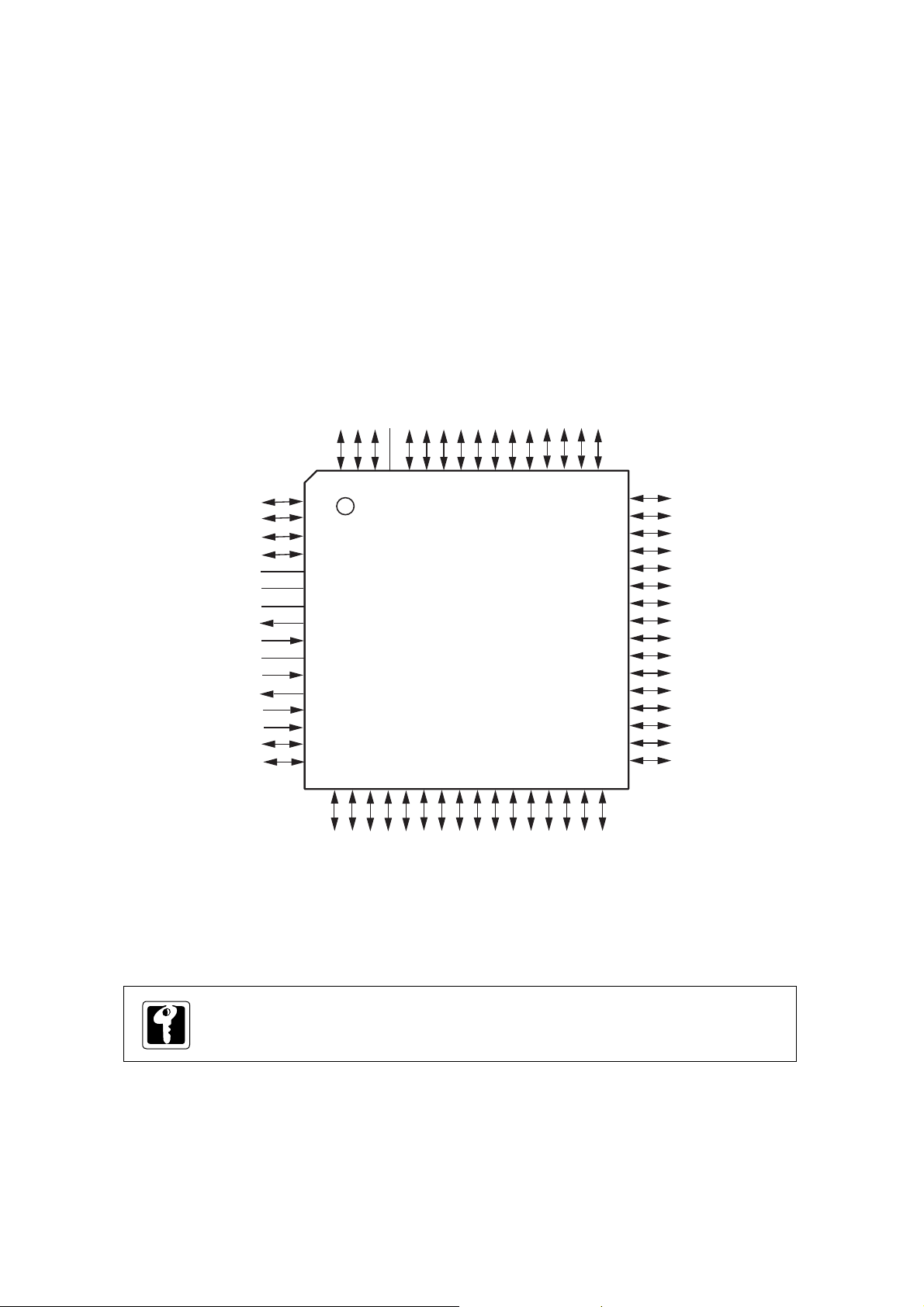
1-3-1 Pin Configuration
Chapter 1 Overview
AN3/PA3
AN4/PA4
AN5/PA5
AN6/PA6
NC(VPP)
VREF+
VDD
OSC2
OSC1
VSS
XI
XO
MMOD
NRST/P27
TXD1A/SBO1A/P00
SDA4B/RXD1A/SBI1A/P01
1
2
3
4
5
6
7
8
9
10
11
12
13
14
15
16
PA2/AN2
PA1/AN1/DA1
636261
64
171819
PA0/AN0/DA0
VREF-
P80/LED0
P81/LED1
P82/LED2
P83/LED3
P84/LED4
P85/LED5
P86/LED6
6059585756555453525150
MN101C77C
- 64 pin for general use -
20
2122232425262728293031
P87/LED7
P77/TCIO5
P76/TCIO1
P75/SBT1B
P74/SBI1B/RXD1B
49
48
47
46
45
44
43
42
41
40
39
38
37
36
35
34
33
32
P73/SBO1B/TXD1B
P72/SBT0B
P71/SBI0B/RXD0B
P70/SBO0B/TXD0B
P67/SDO7/KEY7
P66/SDO6/KEY6
P65/SDO5/KEY5
P64/SDO4/KEY4
P63/SDO3/KEY3
P62/SDO2/KEY2
P61/SDO1/KEY1
P60/SDO0/KEY0
P54/SCL4A
P53/SDA4A
P52/SBT3/SCL3
P51/SB03/SDA3
SBT0A/P05
BUZZER/P06
RXD0A/SBI0A/P04
SCL4B/SBT1A/P02
TXD0A/SBO0A/P03
RMOUTA/TCO0A/P10
IRQ0/P20
TCIO7/P14
TCO4A/P12
TCIO4B/P13
RMOUTB/TCIO0B/P11
IRQ2/P22
ACZ/IRQ1/P21
SBI3/P50
IRQ3/P23
IRQ4/P24
On Flash version of MN101CF77G, NC pin is VPP.
Figure 1-3-1 Pin Configuration ( 64 LQFP/64TQFP : Top view )
Pin Description
I - 9

Chapter 1 Overview
1-3-2 Pin Specification
Table 1-3-2 Pin Specification
Pin
P00 SBO1A TXD1A in/out P0DIR0 P0PLU0 SBO1A : Serial Interface 1 transmission data output TXD1A : UART 1 transmission data output
P01 SBI1A RXD1A in/out P0DIR1 P0PLU1 SBI1A : Serial Interface 1 reception data input
P02 SBT1A in/out P0DIR2 P0PLU2 SBT1A : Serial 1 clock I/O
P03 SBO0A in/out P0DIR3 P0PLU3 SBO0A : Serial 0 transmission data output
P04 SBI0A in/out P0DIR4 P0PLU4 SBI0A : Serial 0 reception data input
P05 SBT0A in/out P0DIR5 P0PLU5 SBT0A : Serial 0 clock I/O
P06 BUZZER in/out P0DIR6 P0PLU6 BUZZER : Buzzer output
P10 TCO0A RMOUTA in/out P1DIR0
P11 TCIO0B in/out P1DIR1 P1PLU1 TCIOOB : Timer 0 I/O
P12 TCO4A in/out P1DIR2 P1PLU2 TCIO4A : Timer 4 I/O
P13 TCIO4B in/out P1DIR3 P1PLU3 TCIO4B : Timer 4 I/O
P14 TCIO7 in/out
P20 IRQ0 P2PLU0 IRQ0 : External interrupt 0
P21 IRQ1 P2PLU1 IRQ1 : External interrupt 1
P22 IRQ2 P2PLU2 IRQ2 : External interrupt 2
P23 IRQ3 P2PLU3 IRQ3 : External interrupt 3
P24 IRQ4 P2PLU4 IRQ4 : External interrupt 4
P27 NRST in/out - - NRST : Reset
P50
P51
P52 SBT3 in/out P5DIR2 P5PLU2 SBT3 : Serial interface 3 clock I/O
P53 in/out P5DIR3 P5PLU3
P54 in/out P5DIR4 P5PLU4
P60 SDO0 in/out P6DIR0 P6PLU0 KEY0 : KEY interrupt input 0
P61 SDO1 in/out P6DIR1 P6PLU1 KEY1 : KEY interrupt input 1
P62 in/out P6DIR2 P6PLU2
P63 SDO3
P64
P65
P66
P67
P70 in/out P7DIR0 P7PLUD0
P71 in/out P7DIR1 P7PLUD1
P72 in/out P7DIR2 P7PLUD2
P73 in/out P7DIR3 P7PLUD3
P74 in/out P7DIR4 P7PLUD4
P75 in/out P7DIR5 P7PLUD5
P76 in/out P7DIR6 P7PLUD6
P77 in/out P7DIR7 P7PLUD7
P80 LED0 in/out P8DIR0 P8PLU0 LED0 : LED driving pin 0
P81 LED1 in/out P8DIR1 P8PLU1 LED1 : LED driving pin 1
P82 LED2 in/out P8DIR2 P8PLU2 LED2 : LED driving pin 2
P83 LED3 in/out P8DIR3 P8PLU3 LED3 : LED driving pin 3
P84 LED4 in/out P8DIR4 P8PLU4 LED4 : LED driving pin 4
P85 LED5 in/out P8DIR5 P8PLU5 LED5 : LED driving pin 5
P86 LED6 in/out P8DIR6 P8PLU6 LED6 : LED driving pin 6
P87 LED7 in/out P8DIR7 P8PLU7 LED7 : LED driving pin 7
PA0 AN0 PAPLUD0 AN0 : Analog 0 input
PA1 AN1 PAPLUD1 AN1 : Analog 1 input
PA2 AN2 PAPLUD2 AN2 : Analog 2 input
PA3 AN3 PAPLUD3 AN3 : Analog 3 input
PA4 AN4 PAPLUD4 AN4 : Analog 4 input
PA5 AN5 PAPLUD5 AN5 : Analog 5 input
PA6 AN6 PAPLUD6 AN6 : Analog 6 input
Function
SDA4B
SBI3
SBO3
SDA4A
SCL4A
SDO2
SDO4
SDO5
SDO6
SDO7
SBO0B
SBI0B
SBT0B
SBO1B
SBI1B
SBT1B
TCIO1
TCIO5
SCL4B
TXD0A
RXD0A
RMOUTB
ACZ
SDA3
SCL3
KEY0
KEY1
KEY2
KEY3
KEY4
KEY5
KEY6
KEY7
TXD0B
RXD0B
TXD1B
RXD1B
DA0
DA1
Input/output
in/out
in/out
in/out
in/out
in/out
in/out P5DIR0 P5PLU0 SBO3 : Serial 3 reception data output
in/out P5DIR1 P5PLU1 SBI3 : Serial interface 3 ransmission data input
in/out P6DIR3 P6PLU3 KEY3 : KEY interrupt input 3
in/out
in/out P6DIR5 P6PLU5 KEY5 : KEY interrupt input 5
in/out
in/out
in/out
in/out
in/out
in/out
in/out
in/out
in/out
Direction
control
P1DIR4 P1PLU4 TCIO7 : Timer 7 I/O
P2DIR0
P2DIR1
P2DIR2
P2DIR3
P2DIR4
P6DIR4
P6DIR6
P6DIR7 P6PLU7 KEY7 : KEY interrupt input 7
PADIR0
PADIR1
PADIR2
PADIR3
PADIR4
PADIR5
PADIR6
Pin control
SDA4B :
Serial Interface 4
P1PLU0 TCIO0A : Timer 0 output
SDA4A : Serial interface 4 data I/O
SCL4A : Serial interface 4 clock I/O
SDO0 : Timer synchronous output 0
SDO1 : Timer synchronous output 1
SDO2 : Timer synchronous output 2
SDO3 : Timer synchronous output 3
SDO4 : Timer synchronous output 4
P6PLU4
SDO5 : Timer synchronous output 5
SDO6 : Timer synchronous output 6
P6PLU6
SDO7 : Timer synchronous output 7
SBO0B : Serial interface 0 transmission data output
SBI0B : Serial interface 0 reception data input
SBT0B : Serial interface 0 clock I/O
SBO1B : Serial interface 1 transmission data output
SBI1B : Serial interface 1 reception data input
SBT1B : Serial interface 1 clock I/O
TCIO1 : Timer 1 I/O
TCIO5 : Timer 5 I/O
Descreption
data I/O
RXD1A : UART 1 reception data output
SCL4B :
Serial Interface 4 clock I/O
TXD0A : UART 0 transmission data output
RXD0A : UART 0 reception data input
RMOUTA : Remote control carrier output
RMOUTB : Remote control carrier output
ACZ : AC zero bolt detection input
SDA3 :
Serial Interface 3 data I/O
SCL3 :
Serial Interface 3 clock I/O
KEY2 : KEY interrupt input 2
KEY4 : KEY interrupt input 4
KEY6 : KEY interrupt input 6
TXD0B : UART 0 transmission data output
RXD0B : UART 0 reception data output
TXD1B : UART 1 transmission data output
RXD1B : UART 1 reception data output
DA0 : DA0 output
DA1 : DA1 output
I - 10
Pin Description

1-3-3 Pin Functions
Table 1-3-3 Pin Function Summary (1/6)
Name No. I/O Funct ion Ot her Funct ion Description
VDD 7 Power supply pin
VSS 10
OSC1 9 Input Clock input pin
OS C 2 8 Output Clock output pin
Supply 1.8 V to 3.6 V to VDD and 0 V to VSS.
Connect these oscillation pins to cer amic or
crystal oscillat ors for high-frequency c loc k
operation.
If the clock is an external input, connect it to OSC1
and leave OSC2 open. T he chip will not oper at e
with an external c lock when using either the
STOP or SLOW modes.
Chapter 1 Overview
XI 11 Input Clock input pin
XO 12 Out put Clock output pin
NRST 14 I/O Reset pin P27 This pin resets the chip when power is turned on,
P00 15 I/O I/O port 0 SBO1A, TXD1A
P01 16 SBI1A, RXD1 A
SDA4B
P02 17 SBT1A , SCL4B
P03 18 SBO0A , T XD0A
P04 19 SBI0A, RXD0 A
P05 20 SBT0A
P06 21 BUZZER
P10 22 I/O I/O port 1 TCO0A, RMOUTA
P11 23 TCIO0B, RMOUTB
P12 24 TCO4A
P13 25 TCIO4B
P14 26 TCI07
Connect these oscillation pins to cer amic
oscillators or crystal oscillators for low-fr equency
clock operation.
If the clock is an external input, connect it to XI
and leave XO open. The c h ip will not operate with
an ex ternal clock when using the STOP mode. If
these pins are not used, connect XI to VSS and
leav e XO open.
is allocated as P27 and contains an internal pullup resistor. S etting this pin low initializes the
internal state of the device. Thereafter, setting the
input to high r eleases the reset. The hardware
waits for t he sy stem clock to stabilize, then
processes the reset int errupt. Also, if ""0" " is
written to P27 and the reset is initiated by
softwar e, a low level will be out put. The output
has an n-channel open-drain configur ation. I f a
capacitor is to be inserted between NRST and
VDD, it is recommended that a discharge diode
be placed between NRST and VDD.
7-Bit CMOS tri-state I/O port.
Eac h bi t can b e set in di vi dual l y as either an in put
or output by the P0DIR register. A pull-up resistor
for eac h bit c an be selected individually by the
P0PLU register.
At reset, the input mode is selected and pull-up
resistors are disabled (high impedance output) .
5-Bit CMOS tri-state I/O port.
Eac h bi t can b e set in di vi dual l y as either an in put
or output by the P1DIR register. A pull-up resistor
for eac h bit c an be selected individually by the
P1PLU register.
At reset, the input mode is selected and pull-up
resistors are disabled (high impedance output) .
Pin Description
I - 11

Chapter 1 Overview
Table 1-3-4 Pin Function Summary (2/6)
Name No. I/O F unctio n Other Function Description
P20 27 I/O I/O port 2 IRQ0
P21 28 IRQ1, ACZ
P22 29 IRQ2
P23 30 IRQ3
P24 31 IRQ4
P27 14 Input I /O port 2 NRST P27 has an n-channel open-drain configurati on.
P50 32 I/O I/O port 5 SBI3
P51 33 SBO3,
P52 34 SBT3
P53 35 SDA4A
P54 36 SCL4A
P60 37 I/O I/O port 6 SDO0, KEY0
P61 38 SDO1, KEY 1
P62 39 SDO2, KEY 2
P63 40 SDO3, KEY 3
P64 41 SDO4, KEY 4
P65 42 SDO5, KEY 5
P66 43 SDO6, KEY 6
P67 44 SDO7, KEY 7
P70 45 I/O I/O port 7 SBO0B, TXD0B
P71 46 SB I0B, RXD0B
P72 47 SBT0B
P73 48 SBO1B, TX D1B
P74 49 SB I1B, RXD1B
P75 50 SBT1B
P76 51 TCI01
P77 52 TCI05
P80 60 I/O I/O port 8 LED0
P81 59 LED1
P82 58 LED2
P83 57 LED3
P84 56 LED4
P85 55 LED5
P86 54 LED6
P87 53 LED7
PA0 62 I/O I/O port A AN0, DA0
PA1 63 AN1, DA1
PA2 64 AN2
PA3 1 AN3
PA4 2 AN4
PA5 3 AN5
PA6 4 AN6
5-Bit CMOS tri-state I/O port.
A pull-up resistor for each bi t can be select e d
individually by the P2PLU register .
At reset, pull-up r esistor s are d isabled
(high impedance output ) .
When "0" is written and the reset is initiated by
softwar e, a low level will be out put.
5-Bit CMOS tri-state I/O port.
Each bit can be set individually as either an input
or output by the P5 DIR register . A pul l-up resistor
for eac h bit c an be selected individually by the
P5PLU register. At reset, the P50t o P54 input
mode is selected and pull- up resistors are
disabled. (high impedance output)
8-Bit CMOS tri-state I/O port.
Each bit can be set individually as either an input
or output by the P6 DIR register . A pul l-up resistor
for eac h bit c an be selected individually by the
P6PLU register.
At reset, the P60 to P67 input mode is selected
and pull- up resistors are disabled.
(high impedance output )
8-Bit CMOS tri-state I/O port.
Each bit can be set individually as either an input
or output by the P7 DIR register . A pul l-up/pulldown resistor for each bit can be selected
individually by the P7PLU r e gist e r . Howev er,
pull-up and pull-down resistors cannot be mixed.
At reset, the P70to P77 input mode is selected
and pull- up resistors are disabled. (high
impedance output )
8-Bit CMOS tri-state I/O port. Each bit can be set
individu al ly as either an input or output by the
P8DIR register. A pull-up resistor for each bit c an
be selected individually by the P8PLU register.
When c o nfigured as out puts, these pins can
drive LEDs directly. A t reset, the P80to P 87 input
mode is selected and pull- up resistors are
disabled. (high impedance output)
6-Bit I/O port. A pull-up or pull-down resistor for
each bi t can be selected individually by the
PAPLUD resister. However, pull-up and pulldown resistors cannot be mixed. At reset, the
PA0 to PA 6 input mode is selected and pull- up
resistor s are di sabled. (high impedance ou tput)
I - 12
Pin Description
 Loading...