

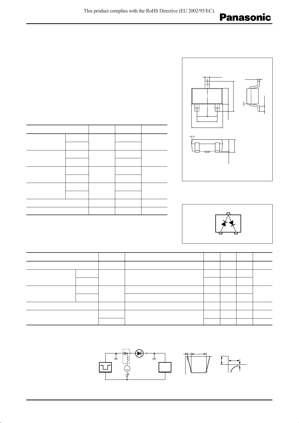
Switching Diodes
This product complies with the RoHS Directive (EU 2002/95/EC).
MA3X153 (MA153), MA3X153A (MA153A)
Silicon epitaxial planar type
Unit: mm
For switching circuits
■ Features
• Small terminal capacitance C
• Two diodes are connected in series in the package
t
■ Absolute Maximum Ratings Ta = 25°C
Parameter Symbol Rating Unit
Reverse voltage
MA3X153
MA3X153A
Maximum peak
reverse voltage
Forward current
MA3X153
MA3X153A
Single I
Series 65
Peak forward
current
Single I
Series 130
Junction temperature T
Storage temperature T
V
R
40
80
V
RM
40
80
F
FM
j
stg
100
200
150 °C
−55 to +150 °C
V
V
mA
mA
(0.95) (0.95)
10˚
EIAJ: SC-59 Mini3-G1 Package
Marking Symbol
• MA3X153: MC • MA3X153A: MP
Internal Connection
1
2.90
+0.10
0.40
–0.05
3
+0.25
–0.05
+0.2
–0.3
2.8
1.50
2
1.9
±0.1
+0.20
–0.05
(0.65)
+0.2
–0.1
1.1
+0.3
–0.1
1.1
+0.10
0.16
–0.06
5˚
1: Anode 1
0 to 0.1
2: Cathode 2
3: Anode 2
Cathode 1
3
0.4±0.2
1
2
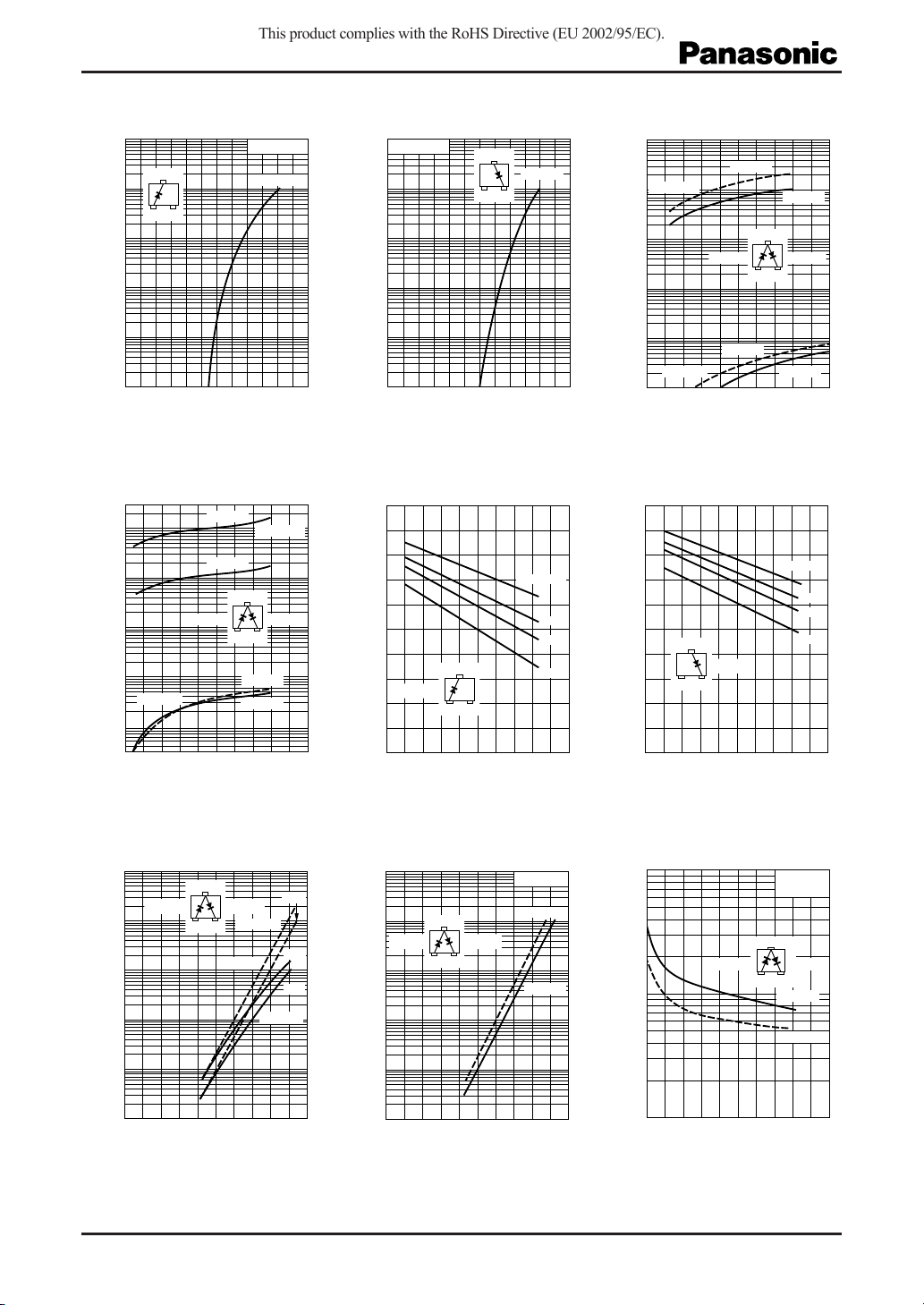
■ Electrical Characteristics Ta = 25°C ± 3°C
Parameter Symbol Conditions Min Typ Max Unit
Forward voltage V
Reverse voltage MA3X153 V
F
R
MA3X153A
Reverse current MA3X153 I
R
MA3X153A
Terminal capacitance C
Reverse recovery time
*
*
t
rr
*
t
rr
3
Note) 1. Measuring methods are based on JAPANESE INDUSTRIAL STANDARD JIS C 7031 measuring methods for diodes.
2. Absolute frequency of input and output is 100 MHz.
3.*1: Between pins 2 and 3
2: Between pins 1 and 3
*
3: trr measurement circuit
*
Pulse Generator
(PG-10N)
= 50 Ω
R
s
Publication date: February 2005 SKF00036DED
IF = 100 mA 1.2 V
IR = 100 µA40V
80
VR = 40 V 100 nA
VR = 75 V 100
VR = 0 V, f = 1 MHz 5.0 pF
t
1
IF = 10 mA, VR = 6 V 150 ns
2
Irr =
Bias Application Unit (N-50BU)
A
, RL = 100 Ω 9ns
0.1 I
R
Input Pulse Output Pulse
t
t
p
Wave Form Analyzer
(SAS-8130)
Ri = 50 Ω
r
10%
V
R
t
t
δ = 0.05
90%
= 2 µs
p
= 0.35 ns
r
t
I
F
I
= 10 mA
F
= 6 V
V
R
= 100 Ω
R
L
t
rr
I
rr
= 0.1 I
t
R
Note) The part numbers in the parenthesis show conventional part number.
1
MA3X153, MA3X153A
This product complies with the RoHS Directive (EU 2002/95/EC).
IF V
F
Ta = 25°C
D
1
)
mA
(
F
3
10
D1 (1-3)
2
10
3
2
1
10
1
Forward current I
−1
10
−2
10
0 0.2 0.4 0.6 0.8 1.0 1.2
Forward voltage VF (V
V
R
10
)
1
µA
(
R
−1
10
−2
10
Reverse current I
Ta = 25°C
−3
10
D1 (1-3)
D2 (3-2)
D1 (1-3
)
3
1
D1 (1-3)
D2 (3-2)
Ta = 125°C
D
2
0 20406080100
Reverse voltage VR (V
(1-3)
)
(3-2
2
)
IF V
D2 (3-2)
1
VF T
3
2
1
3
F
2
a IR
D
(3-2)
2
)
IF = 10 mA
3 mA
1 mA
0.1 mA
3
10
Ta = 125°C
2
10
)
µA
(
R
10
1
Reverse current I
−1
10
−2
10
0 1020304050
1.0
0.8
)
V
(
F
0.6
0.4
Forward voltage V
0.2
0
−40 0 40 80 120 160
)
3
10
Ta = 25°C
2
10
)
mA
(
F
10
1
Forward current I
−1
10
−2
10
0 0.2 0.4 0.6 0.8 1.0 1.2
Forward voltage VF (V
1.0
0.8
)
V
(
F
0.6
)
0.4
Forward voltage V
D
(1-3)
1
0.2
0
−40 0 40 80 120 160
Ambient temperature Ta (°C
IR V
R
D1 (1-3
)
D2 (3-2
3
D
2
1
2
D1 (1-3)
Ta = 25°C
D2 (3-2)
Reverse voltage VR (V
VF T
a
IF = 10 mA
3
D
(3-2)
2
1
2
0.1 mA
Ambient temperature Ta (°C
)
(3-2)D1 (1-3)
)
3 mA
1 mA
)
T
a
3
3
D
2
1
D1 (1-3)
(3-2)D1 (1-3)
2
VR = 80 V
40 V
80 V
10
2
10
)
D
µA
(
R
10
)
nA
(
2
10
10
R
1
40 V
−1
10
Reverse current I
−2
10
−3
10
−40 0 40 80 120
Ambient temperature Ta (°C
D2 (3-2)
1
Reverse current I
−1
10
−2
10
)
2
IR T
a IR
V
= 40 V
R
D
(1-3)
3
(1-3
)
1
D2 (3-2
2
1
1
)
D
(3-2)
2
−40 0 40 80 120
Ambient temperature Ta (°C
SKF00036DED
Ct V
10
)
pF
(
t
1
R
f = 1 MHz
= 25°C
T
a
(
)
(
1-3
D
1
132
)
3-2
D
2
(
)
D
3-2
2
(
)
1-3
D
1
Terminal capacitance C
−1
10
0 1020304050
)
Reverse voltage VR (V
)
 Loading...